performance analysis and improvement for hybrid … analysis an… · performance analysis and...
TRANSCRIPT

RESEARCH CENTRE FOR INTEGRATED MICROSYSTEMS - UNIVERSITY OF WINDSOR
Performance Analysis and Improvement for Hybrid CMOS-SET Circuitfor Hybrid CMOS SET Circuit
Architectures
Author: Guoqing DengInstructor: Dr. Chunhong Cheng
Email: [email protected]: 319C Essex Hall University of Windsor
1

RESEARCH CENTRE FOR INTEGRATED MICROSYSTEMS - UNIVERSITY OF WINDSOR
O iOverview• Research Background - Why nanotechnology.g y gy• Structure of SET transistor and Coulomb Blockade Oscillation.• Why hybrid CMOS-SET circuits – Comparison between CMOS and
SET.SET.• Simulation methodology of hybrid CMOS-SET circuits.• Two of the most popular hybrid CMOS-SET architectures – serial
SETMOS and parallel SETMOSSETMOS and parallel SETMOS.• Analysis and compare of serial and parallel SETMOS in terms of
power dissipation, drivability, and temperature effect.Voltage biased parallel SETMOS ith impro ed temperat re effect• Voltage-biased parallel SETMOS with improved temperature effect.
• Implementation examples using parallel SETMOS architecture –Hybrid CMOS-SET NOR gate.
2

RESEARCH CENTRE FOR INTEGRATED MICROSYSTEMS - UNIVERSITY OF WINDSOR
Research Background Introduction
• Moore’s LawThe number of transistors on a chip will double about every two years.
The scale-down of the size of MOSFET transistorsaccording to Moore's law has taken place for the last 40years, so far it has entered the deep sub-50 nm regime.The more transistors on a chip the higher performance
3
The more transistors on a chip, the higher performanceand the lower cost of circuits are.

RESEARCH CENTRE FOR INTEGRATED MICROSYSTEMS - UNIVERSITY OF WINDSOR
Research Background Introduction
• CMOS scale-down limitsPhysical limitQuantum effects and non-deterministic behavior.- Never overcomeTechnical limitPower dissipation, process variation, second-order effects, and design complexity.- Can be overcome but difficult- Can be overcome, but difficultEconomic limitUpdate of facilities and techniques.
4
p q- Can be overcome, but expensive

RESEARCH CENTRE FOR INTEGRATED MICROSYSTEMS - UNIVERSITY OF WINDSOR
Research Background Introduction
• Nanoelectronics – next generation technology.Definition of nanoelectronics:
Digital and signal-processing electronics, informationg g p g ,storage devices, and electronic sensors that achieveenhanced performance by reducing feature sizesbelow 100 nmbelow 100 nm.
In the field of nanoelectronics, people are able to controlthe movement and position of a small number of electronsthe movement and position of a small number of electronsinstead of current with thousands of electrons.
5

RESEARCH CENTRE FOR INTEGRATED MICROSYSTEMS - UNIVERSITY OF WINDSOR
Research Background Introduction
• Emerging Nano-Devices: Life after CMOS
Single electron transistor (SETs)Nanotube (CNTs)NanowiresResonant tunneling diode (RTD)Resonant tunneling diode (RTD)Rapid single quantum flux (RSQF)Nanoelectromechanical systems (NEMS)Nanoelectromechanical systems (NEMS)Molecular devices
6

RESEARCH CENTRE FOR INTEGRATED MICROSYSTEMS - UNIVERSITY OF WINDSOR
Research Background Introduction
• Single electron transistor (SETs)Single electron transistor (SETs)Advantages:
N l f t iNano-scale feature size;Ultra-low power dissipation;Coulomb Blockade Oscillation;Coulomb Blockade Oscillation;
SET is more promising for future VLSI design. Its majorapplications are memory, multiple valued logic, and neuralnetworks.
7

RESEARCH CENTRE FOR INTEGRATED MICROSYSTEMS - UNIVERSITY OF WINDSOR
SET transistor and its work principles
• SET structure
8

RESEARCH CENTRE FOR INTEGRATED MICROSYSTEMS - UNIVERSITY OF WINDSOR
SET transistor and its work principles
• Coulomb Blockade Oscillation
Parameters: IDC = 2nA; Cg1 = Cg2 = 2aF; Ctd =
The frequency of the oscillation is e/Cg1 = 80mV.
Ctd =1aF; Rtd = Rts = 1M; Cload = 10fF; T = 10K;
9

RESEARCH CENTRE FOR INTEGRATED MICROSYSTEMS - UNIVERSITY OF WINDSOR
Why hybrid CMOS-SET circuits
Disadvantages of SET:• Low current-drivability;y;• Small voltage-gain;• Low-temperature operation;
Advantages of CMOS:Advantages of CMOS:• High-speed current drive;• High gain;• Room temperature operation;
It is shown that CMOS devices have advantages that can compensate for the intrinsic drawbacks of SET.
Although a complete replacement of CMOS by single electrics is unlikely inthe near future, it is true that by combining SET and CMOS, we can bring outnew functionalities which are not mirrored in pure CMOS technology.p gy
10

RESEARCH CENTRE FOR INTEGRATED MICROSYSTEMS - UNIVERSITY OF WINDSOR
Simulation methodology of hybrid CMOS-SET circuits
• SIMON – SET-based circuit simulator• SIMON – SET-based circuit simulator– Most accurate SET circuit simulator.– Integrate Monte Carlo method and Master Equations, calculating the
probabilities of tunneling eventsprobabilities of tunneling events. – Time consuming, especially there is current source in the circuit.– Not suitable for large scale complex circuits.
C t i l t ith MOSFET– Cannot co-simulate with MOSFETs.
• SPICE macro models– Using equivalent circuits based on conventional SPICE componentsUsing equivalent circuits based on conventional SPICE components. – SPICE compatible and able to co-simulation with MOSFETs.– Non-physical and empirical in nature.
11

RESEARCH CENTRE FOR INTEGRATED MICROSYSTEMS - UNIVERSITY OF WINDSOR
Simulation methodology of hybrid CMOS-SET circuits
• MIB compact modelMIB compact model– Most accurate model for hybrid CMOS-SET circuit.– Using current equations to describe the behavior of SET.
SPICE compatible and able to co simulation with MOSFETs– SPICE compatible and able to co-simulation with MOSFETs.– Integrate thermal components and physical parameters.– Developed by AHDL and can be implemented in the SPICE simulator
though VerilogA interfacethough VerilogA interface.
Assumption:The interconnect capacitances associated with drain, source and gatep , gterminals of SET are much larger than the device capacitances (that isC∑ = Ctd + Cts + Cg1 +Cg2) which ensures there is no interactionbetween interconnected SETs.
12

RESEARCH CENTRE FOR INTEGRATED MICROSYSTEMS - UNIVERSITY OF WINDSOR
Two of the most popular hybrid CMOS-SET architectures
• Serial and parallel SETMOSSerial and parallel SETMOS
If increasing input voltage of VIN in both architectures, there will belt ill ti t d i t i l f SET d thi lt ill ti
13
voltage oscillation at drain terminal of SET, and this voltage oscillationcan be transferred to the output node.

RESEARCH CENTRE FOR INTEGRATED MICROSYSTEMS - UNIVERSITY OF WINDSOR
Two of the most popular hybrid CMOS-
• If tuning VGG for serial SETMOS or tuning VSS for parallel
SET architecturesIf tuning VGG for serial SETMOS or tuning VSS for parallelSETMOS to bias NMOS transistor in the sub-threshold region,the amplitude of voltage oscillation at drain terminal of SET canbe amplified at output node which is suitable for CMOS circuits.
14

RESEARCH CENTRE FOR INTEGRATED MICROSYSTEMS - UNIVERSITY OF WINDSOR
Two of the most popular hybrid CMOS-SET architectures
• Parameters SelectionParameters Selection– For all SETs, Ctd = Cts = 0.1aF; Cg1 = Cg2 = 0.13aF.– For all NMOS transistors, W = 500nM; L = 180nM.
Other parameters are shown in the table:Other parameters are shown in the table:
In the following experiments,these parameters will be usedotherwise specified.otherwise specified.
To ensure the reasonable dynamic range of output voltage oscillation, the value of current connected to the SET cannot be set too large.V is used to adjust the phase of Coulomb blockade oscillation with
15
VCtrl is used to adjust the phase of Coulomb blockade oscillation with no effect on the amplitude and frequency of the output.

RESEARCH CENTRE FOR INTEGRATED MICROSYSTEMS - UNIVERSITY OF WINDSOR
Two of the most popular hybrid CMOS-SET architectures
• DC analysis for both serial and parallel SETMOS– Using above parameters and at temperature of 20°C.
•VIN is input voltage changingfrom 0 to 1.8V.from 0 to 1.8V.•Vtmp is the voltage at drainterminal of SET;•Vout1 is the output voltagesof serial SETMOS.o se a S OS•Vout2 is the output voltagesof parallel SETMOS.
It can be seen that the voltage at the outputs of both serial and parallelSETMOS oscillates with amplified magnitude of 1 7V and the periodicity of
16
SETMOS oscillates with amplified magnitude of 1.7V and the periodicity ofe/CG1 = 1.25V in the scale of input voltage.

RESEARCH CENTRE FOR INTEGRATED MICROSYSTEMS - UNIVERSITY OF WINDSOR
Analysis and compare of serial and parallel SETMOSSETMOS
• Power Dissipation• Power Dissipation– For MOSFETs, the power dissipation is dominated by
the dynamic power during logic transition region wherethere is a current from VDD to ground.
– For SETs, the most power dissipation is static power atnon transition regions where the output is logic 0 or 1non-transition regions where the output is logic 0 or 1.
This is because for SET circuits, even though the numberof electrons in the island of each SET is constant at theof electrons in the island of each SET is constant at thestatic state, there are still electrons tunneling in and out ofthe island which contribute to the static power dissipation.
17

RESEARCH CENTRE FOR INTEGRATED MICROSYSTEMS - UNIVERSITY OF WINDSOR
Analysis and compare of serial and parallel SETMOSSETMOS
• To calculate the total power dissipation, – Run transient analysis at temperature of 20°C.
•VIN is ideal clock signal with thevoltage swing of 450mV and theperiod of 2µs.•Vtmp is the voltage at drainterminal of SET;•Vout1 is the output voltages ofserial SETMOS.•Vout2 is the output voltages ofparallel SETMOS.
It is shown that serial SETMOS functions as an inverter while the parallel SETMOS acts as a buffer
18
parallel SETMOS acts as a buffer

RESEARCH CENTRE FOR INTEGRATED MICROSYSTEMS - UNIVERSITY OF WINDSOR
Analysis and compare of serial and parallel SETMOSSETMOS
We can calculate power dissipation by integrating output voltage curve timingvoltage curve, timing with constant current value, and dividing by th i d
It was found that:For serial SETMOS it has ultra low power dissipation of 35 1nW due
the period.
– For serial SETMOS, it has ultra low power dissipation of 35.1nW dueto small constant current IDC.
– For parallel SETMOS, however, the total power dissipation turns outto be as high as 676 5nw which is dominated by the power of NMOSto be as high as 676.5nw which is dominated by the power of NMOStransistor (665.5nW).
19

RESEARCH CENTRE FOR INTEGRATED MICROSYSTEMS - UNIVERSITY OF WINDSOR
Analysis and compare of serial and parallel SETMOS
• Drivability
SETMOSDrivabilityThe drivability of both serial and parallel SETMOS can be tested by adding a load capacitance at the output node.
•Run transient analysis attemperature of 20°C withincreasing load capacitance.•Use ideal clock signal withgthe voltage swing of 450mVand the period of 2µs. asinput voltage.
It is shown that:– For serial SETMOS, it can only drive a capacitive load of several fFs.
20
For serial SETMOS, it can only drive a capacitive load of several fFs.– For parallel SETMOS, the drivability is up to several hundreds of fFs.

RESEARCH CENTRE FOR INTEGRATED MICROSYSTEMS - UNIVERSITY OF WINDSOR
Analysis and compare of serial and parallel SETMOS
• Temperature Effect
SETMOS
• Temperature Effect– For pure SET circuit, it can only work at extremely low
temperature (usually less than 100K). The higher thetemperature, the smaller the amplitude of CoulombBlockade Oscillation.
F i l d ll l SETMOS th k t– For serial and parallel SETMOS, they can work atmuch higher temperature if the NMOS transistor isbiased to work in the sub-threshold region. This isbecause the MOSFET has a large voltage gain whichcan amplify the tiny swing of SET output to anacceptable levelacceptable level.
21

RESEARCH CENTRE FOR INTEGRATED MICROSYSTEMS - UNIVERSITY OF WINDSOR
Analysis and compare of serial and parallel SETMOS
• Temperature Effect
SETMOS
• Temperature EffectHowever, both serial and parallel SETMOS are very sensitive to the temperature variation.
•Run transient analysis withtemperature changing from10°C to 30°C in the step of5°C5 C.•Use ideal clock signal withthe voltage swing of 450mVand the period of 2µs. asinput voltageinput voltage.
22

RESEARCH CENTRE FOR INTEGRATED MICROSYSTEMS - UNIVERSITY OF WINDSOR
Analysis and compare of serial and parallel SETMOS
• Temperature Effect
SETMOS
As temperature increases:As temperature increases:– VTH of NMOS transistor reduces.– The peak voltage of SET oscillation at the drain terminal of SET reduces.
The alle oltage of SET oscillation remains almost the same
23
– The valley voltage of SET oscillation remains almost the same.– The slope of VDS vs. VGS curve for current-biased NMOS transistor goes down.
RESEARCH CENTRE FOR INTEGRATED MICROSYSTEMS - UNIVERSITY OF WINDSOR
Analysis and compare of serial and parallel SETMOSSETMOS
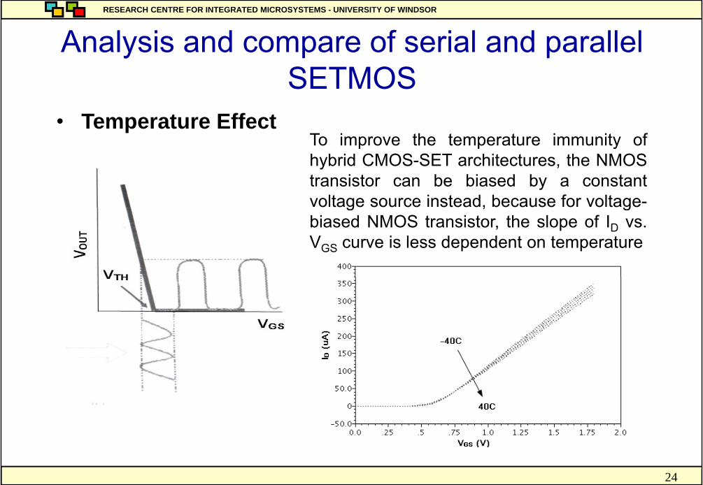
• Temperature EffectTo improve the temperature immunity ofTo improve the temperature immunity ofhybrid CMOS-SET architectures, the NMOStransistor can be biased by a constantvoltage source instead, because for voltage-g , gbiased NMOS transistor, the slope of ID vs.VGS curve is less dependent on temperature
24

RESEARCH CENTRE FOR INTEGRATED MICROSYSTEMS - UNIVERSITY OF WINDSOR
Analysis and compare of serial and parallel SETMOS
• Voltage-biased parallel SETMOS
SETMOSVoltage biased parallel SETMOS– Have better temperature performance.– Parameters are the same as before except VDD = 1V and VSS = –266mV.
The size of extra NMOS transistor is set as W/L = 0 5μm/3 2μm– The size of extra NMOS transistor is set as W/L = 0.5μm/3.2μm.
25

RESEARCH CENTRE FOR INTEGRATED MICROSYSTEMS - UNIVERSITY OF WINDSOR
Analysis and compare of serial and parallel SETMOS
Summary:
SETMOS
For serial SETMOS:• Very low power dissipation• Weak drivability• Room temperature operation, but much sensitive.
For parallel SETMOS (current-biased):• More power dissipationMore power dissipation• High drivability• Room temperature operation, but much sensitive.
For improved parallel SETMOS (voltage-biased):For improved parallel SETMOS (voltage-biased):• Very large power dissipation• High drivability
Room temperat re operation and not sensiti e• Room temperature operation, and not sensitive.
26

RESEARCH CENTRE FOR INTEGRATED MICROSYSTEMS - UNIVERSITY OF WINDSOR
Implementation examples using parallel SETMOS hit tSETMOS architecture
• Hybrid CMOS-SET NOR gate• Hybrid CMOS-SET NOR gate.– Using parallel SETMOS architecture where IDC1 = 30nA, IDC2 = 1uA,
VCtrl = 650mV, VSS = –380mVThe rest of parameters are the same as before– The rest of parameters are the same as before.
27

RESEARCH CENTRE FOR INTEGRATED MICROSYSTEMS - UNIVERSITY OF WINDSOR
Implementation examples using parallel SETMOS hit t
• Hybrid CMOS-SET NOR gate.
SETMOS architecture Hybrid CMOS SET NOR gate.– The power dissipation is only 147.6nW in comparison with pure
CMOS NOR gate which is several uW. – It has very large drivability and can work at room temperature inIt has very large drivability and can work at room temperature in
comparison with pure SET NOR gate which has very low drivability and can only work at extremely low temperature.
Therefore the hybrid CMOS-SET NOR gate shares the merits of bothTherefore, the hybrid CMOS-SET NOR gate shares the merits of both CMOS and SET circuits.
• Hybrid CMOS-SET NAND gate.If NMOS t i t i h b id CMOS SET NOR t i bi d b iIf NMOS transistor in hybrid CMOS-SET NOR gate is biased by using voltage source and extra NMOS transistor connected in, a hybrid CMOS-SET NAND gate can be realized as well.
It has much better temperature performance than hybrid CMOS SET– It has much better temperature performance than hybrid CMOS-SET NOR gate.
28

RESEARCH CENTRE FOR INTEGRATED MICROSYSTEMS - UNIVERSITY OF WINDSOR
Thank YouThank You
29