photoconductive and optical properties of amorphous selenium · photoconductive and optical...
TRANSCRIPT
PHOTOCONDUCTIVE AND OPTICAL PROPERTIES OF AMORPHOUS SELENIUM
by John A. Woollam, Kenneth R. Morasb, Mitchell Kzlninsky, and Benjamin L. Averbach
Lewis Research Center Cleveland, Ohio 44135
N A T I O N A L A E R O N A U T I C S A N D S P A C E A D M I N I S T R A T I O N W A S H I N G T O N , D. C. S E P T E M B E R 1971
https://ntrs.nasa.gov/search.jsp?R=19710025450 2018-08-29T04:26:15+00:00Z
TECH LIBRARY KAFB, NM
1. Report No. NASA TN D-6500
. .~
4. Title and Subtitle
PHOTOCONDUCTIVE AND OPTICAL PROPERTIES OF AMORPHOUS SELEMUM
7. Author(s) John A. Woollam, Kenneth R. Morash, Mitchel Kuninsky, and Benjamin L. Averbach
9. Performing Organization Name and Address
Lewis Research Center National Aeronautics and Space Administration Cleveland, Ohio 44135
12. Sponsoring Agency Name and Address
National Aeronautics and Space Administration Washington, D.C. 20546
15. Supplementary Notes
16. Abstract
6. Performing Organization Code
8. Performing Organization Report No.
E-6302 10. Work Unit No.
129-02 11. Contract or Grant No.
13. Type of Report and Period Covered
Technical Note 14. Sponsoring Agency Code
The electron and hole drift mobilities in photoconducting amorphous selenium were measured. Samples were prepared by vapor deposition on substrates held both above and below the selenium glass transition temperature T This report makes several contributions to
g' understanding mobility: we have shown that the substrate deposition temperature has little effect on the mobility at 300 K. However, from the temperature dependence of the hole mobility, a thermal activation energy of 0.20*0.02 eV was observed for samples deposited below Tg. This is higher than previously reported for samples deposited near T Mobility is
g ' found to be independent of magnetic fields to 1tesla within an accuracy of -+-5percent. Mobility at 300 K is also shown to be independent of wavelength from 0.22 to 0.60 micrometer; however, the number of ca r r i e r s is very dependent on wavelength, and this determines the wavelength cutoff in the number of ca r r i e r s excited to mobile states. The photoconductivity edge was found near 0 .5 micrometer and the optical absorption edge between 0.66 and 0.90 micrometer. In addition, we have studied the influence of the methods of preparation of electrode films. A new phenomenon has been investigated for temperatures below 200 K, where voltage-against -time curves a r e exponential, rather than kinked, and the exponential decay is strongly temperature dependent. Another unusual result was that the electron mobility changed by a factor of 3 for electric fields greater than 5x10⁶ V/m.
17. Key Words (Suggested by Author(s)) 18. Distribution Statement
Selenium Temperature dependence Unclassified - unlimited Photoconductivity Preparation dependence Optical properties Drift mobility
.~
19. Security Classif. (of this report) 20. Security Classif. (of this page) 21. NO. of Pages 22. Price'
Unclassified Unclassified 27 $3.00
PHOTOCONDUCTIVE AND OPTICAL PROPERTIES OF AMORPHOUS SELENIUM
by John A. Woollam, K e n n e t h R. Morash*, M i t c h e l l Kuninsky*, and Benjamin L. Averbach*
Lewis Research Center
SUMMARY
The electron and hole drift mobilities in photoconducting amorphous selenium were measured at 300 K . Only small differences were observed between samples deposited on substrates below the glass temperature T of 313 K and those deposited on sub
gstrates above T Mobility values were found, within experimental e r ro r , to be the
g' same as the values found by others for samples deposited on substrates held above the glass temperature. We have measured a sharp drop in the number of mobile charges for wavelengths between 0. 48 and 0.52 micrometer and longer. The optical absorption edge was found to be between 0.66 and 0.90 micrometer. A thermal activation energy for hole mobility was determined from the temperature dependence of mobility to be 0.2050.02 electron volts. This is higher than the values for our samples deposited near
Tg. A temperature dependence, previously not observed, of photogenerated voltage decay, was found for temperatures between 130 and 220 K. This may be related to a phenomenon observed recently by Tabak (ref. 1). The mobility at 300 K was independent of wavelength and of magnetic field to 1 tesla. As a necessary part of the research the optical absorption of thin-film electrode material was studied.
INTRODUCTlON
Amorphous (semiconducting) selenium is used for electro-static imaging, as well as for photovoltaic cells, in the visible region of the electromagnetic spectrum. The photoconductive properties determine how effective and fast responding the material will be; that is, the higher the mobility, the faster the response and the faster the material can be optically scanned. It is hoped that a study of the photoconductive properties will lead to more efficient materials. In addition, it would be of practical importance to develop materials sensitive over a wide region of wavelengths.
* Staff of the Department of Metallurgy and Materials Science, Massachusetts Institute of Technology, Cambridge, Massachusetts.
Amorphous semiconductors a r e also of great current interest because of their switching properties on the application of high voltages (ref. 2). There is a need to test the models of these materials for the energy band structure and for the density of states near the energy band gap. The development of consistent theoretical models for amorphous semiconductors will help in understanding present materials and devices, and aid in predicting new uses for these materials. Previous studies in amorphous selenium include work by Fotland (ref. 3), Hartke (ref. 4), Grunwald and Blakney (ref. 5 ) , and Speer (ref. 7) . Most of the experimental methods we have used have been used by others (refs. 3 to 7) .
In this report measurements of drift mobility a r e described for both electrons and holes in amorphous selenium. These values a r e compared with values found by others (refs. 4 to 8). In addition, we have measured the mobility as a function of temperature and looked for changes as a function of magnetic field and wavelength. We have attempted to understand why various samples give better "signals" than others, and why samples from the same initial deposition have somewhat different characteristics. We performed a number of related experiments designed to improve the experimental method and to provide a better understanding of the results. For example, the optical absorption of the electrodes used for voltage contacts was measured, and these results were found to be significant. The optical absorption of selenium out to 50 micrometers in the far infrared was measured to search for any absorption "resonances. l t
A study of the effects of material preparation methods was made. Samples were deposited on substrates held both above and below the glass temperature T The glass
'gtemperature is defined as the second-order phase transition occurring between 303 K and 316 K. Among the more evident changes at T a r e the mechanical properties. Below T selenium is brittle, and above T it is
g ductile (Dr.A . R. Melnyk, privateg g
communication). In going from T < T to T > T the viscosity drops by several g g
orders of magnitude. The work reported herein was performed during the summer of 1970 at MIT where
John Woollam was a visiting scientist in the department of Metallurgy and Materials Science. Samples and helpful information were supplied by Drs. Evan J. Felty, M a r k D. Tabak, Mark B. Myers, and Andrew R. Melnyk.
*
THEORY
Photoconduction
The effectiveness of selenium in devices depends on the photoconductive properties and especially the drift mobility of the car r ie rs . The drift mobility pd is the velocity
2
"response" of charges to an applied electric field (ref. 9):
V
'Id=Fi -
where v is the velocity of the charge and E is the applied electric field. (All symbols are defined in appendix A. ) If the sample has a flat plate geometry of thickness d with an apphed voltage Vo across the thickness, we have
'Id =-vd
vO
Assuming the charge moves across the plate with a constant velocity,
where t is the time taken to t raverse the thickness d. Typical transit times are of the order of second. If charges make collisions or are momentarily trapped and then released in times much less than Second, the transit velocity will be nearly constant during the transit time. (See appendix B for a general derivation. ) Trapping is discussed in reference 10.
To make a meaningful measurement of mobility, the electric field across the sample must be uniform. This assumes that there a re no charges existing in the bulk of the sample. Selenium in the dark state exhibits a low conductivity (p - 1010 ohm-m, ref. 2) and trapped charges can exist within the bulk for a long time. To make meaningful mobility measurements, it is thus necessary to induce the generation of very thin layers of photogenerated charge. This requires that a charge layer is created on the surface with thickness K such that
K << d (4)
The incident light ionizes the selenium atoms, creating negative electrons and positive hole carr iers . With a large enough applied voltage Vo, it is possible to make these charges t raverse the thickness of the sample before recombining to neutralize. (See derivation in appendix B. ) Depending on the polarity of Vo, it is possible to have either the positive charges or the negative charges traverse the sample. In amorphous selenium it happens that the mobility for holes (+ charge) is greater by a factor of about
3
30 than the mobility for electrons (- charge). The reason for this is probably related to the atomic arrangement of the amorphous material and to the nature of the traps. By amorphous we mean disordered or noncrystalline. However, amorphous semiconductors have considerable short-range order. A model for the structure of amorphous selenium has been determined from X-ray diffraction by Kaplow, Rowe, and Averbach (ref. 10). The structure was found to be composed almost entirely of eight-member rings, in an atomic arrangement which was only a slight perturbation of crystalline monoclinic selenium. Some of the rings in the amorphous material are opened slightly and these openings may be very effective trapping centers for electrons.
The amorphous state is thus closely related to the crystalline state of the same material and Mott (ref. 2) and Cohen (ref. l l ) , for example, have proposed that the energy bands near the band gaps are related. Figure 1 shows the density of energy
Crvstal l ine
_ -E
Figure 1. - Band model for density of states in amorphous semiconductors. (From ref. 11. )
states as a function of energy for this model as discussed by Cohen (ref. 11). In the crystalline state the intrinsic semiconductor has sharp density-of-state "edges, " where the density of states drops to near zero as a function of energy. The lower occupied energy region is the valence band and the unoccupied higher energy region is the conduction band. These are separated by an energy gap EC In the amorphous
g'state the model suggested is one in which the sharp edges are rounded and the gap contains localized energy states.
Carr iers can be optically excited into the conduction band of crystalline materials in several ways. One of these is the following: Tf there a re no impurity states, the incident radiation may ionize an atom, thus giving the electror, enough energy to be free to conduct electric current. This requires incident radiation energy equal to o r greater than the energy gap. In crystalline selenium this is approximately 1 . 8 electron volts (ref. 12). The incident light energy is quantized into photon units; and if one photon excites one electron into the conduction band, the quantum efficiency is said to be unity. It is important in electro-optic materials t o have a high quantum efficiency.
4
The efficiency of practical materials depends on the wavelength of the radiation and can be between zero and unity, depending on specific definition of quantities.
In amorphous materials, electrons can be excited across the (now fuzzy) energy gap, between localized states within the band gap, or from the valence to the conduction band. With fuzzy energy gaps, photoconduction and optical absorption edges will be not as sharp in amorphous as in crystalline materials (ref. 13).
In crystalline intrinsic semiconductors the energy gap can be measured by measuring t h e electrical conductivity as a function of temperature. In these experiments the conductivity is measured using the car r ie rs in the conduction band obtained from thermal excitation across the gap. The occupation of conduction band states depends on the temperature through the Boltzmann distribution function k. Thus the conductivity is exponentially dependent on temperature, with an excitation energy corresponding to the energy gap.
In high-resistivity amorphous materials the temperature dependence of the conductivity is not so clearly related to the energy gap because the conduction may be limited by trapping (ref. lo), which is very temperature dependent. Charges are momentarily bound or trapped to localized states in the band gap. Because of thermal activation and the presence of an electric field, the charges remain bound for only short periods of time.
In high-resistivity amorphous semiconductors the thermal activation energy is obtained from mobility-against-temperature plots expressed in the form
The value of E may correspond, for electron carr iers , to the difference between localized energy states in the band gap and the conduction band energy. If trapping dominates the temperature dependence of the mobility, E will be small in comparison with the band gap.
OpticaI Properties
Closely related to the photoconductive properties in amorphous semiconductors a re the optical properties, especially the absorption of radiation of various frequencies. In crystalline materials, light is absorbed whenever electrons a re excited across the energy gap or excited into impurity states. The cutoff frequency for exciting car r ie rs into the conduction band is very sharp for crystalline materials. In amorphous materials the optical absorption edge is smeared out because of the fuzziness of the gap shown in figure 1. The wavelength at which optical absorption is cut off is not always
5
the same as the wavelength for cutoff of photoconduction. This is probably due to excitation of electrons to localized states in optical absorption. These electrons were effective in absorbing radiation but are not excited to high enough energy to be free to conduct current in the photoconductive process. This can cause the optical edge to be at longer wavelengths than the photoconductive edge.
EXPERIMENTAL METHODS
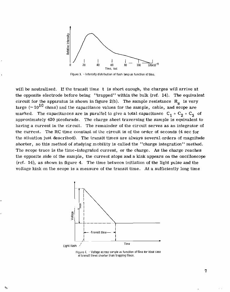
A block diagram of the apparatus is shown in figure 2. A dc voltage variable from 0 to 180 volts (in certain cases up to 1000 V) of either polarity is maintained across the sample. With no light incident there are few car r ie rs , and the current drawn is negligible. Light from a xenon flash lamp is incident through a semitransparent electrode onto the sample surface. The light duration is very short; a time distribution of the pulse intensity is shown in figure 3. The light flash ionizes the sample atoms, creating negative electron charges and positive charged holes. One polarity of charge is free to be accelerated across the sample by the voltage Vo and the charge of opposite polarity
Remote flashfi control 1 Optical filters:
Nanoseconrflashlamp
Lens
3 to 180 v
High-speed oscilloscope
Ampli f iers
-Sample (xl, x10, or ~ 1 0 0 )
Temperature-controlled cryostat
(a) Schematic.
5 MR
(b) Equivalent circuit .
Figure 2. - Photoconductivity apparatus. (See figs. 3 and 6 for characterist ics of flash lamp. 1
6
I 1111
i
t
Time, sec
Figure 3. - In tens i ty distr ibution of flash lamp as function of time.
will be neutralized. If the transit time t is short enough, the charges will arr ive at the opposite electrode before being "trapped" within the bulk (ref. 14). The equivalent circuit for the apparatus is shown in figure 2(b). The sample resistance R, is very large (- lo1' ohms) and the capacitance values for the sample, cable, and scope are marked. The capacitances are in parallel to give a total capacitance C1+ C2 + C3 of approximately 420 picofarads. The charge sheet traversing the sample is equivalent to having a current in the circuit. The remainder of the circuit serves as an integrator of the current. The RC time constant of the circuit is of the order of seconds (4 sec for the situation just described). The transit times a re always several orders of magnitude shorter, s o this method of studying mobility is called the "charge integration" method. The scope trace is the time-integrated current, or the charge. As the charge reaches the opposite side of the sample, the current stops and a kink appears on the oscilloscope (ref. 14), as shown in figure 4. The time between initiation of the light pulse and the voltage kink on the scope is a measure of the transit time. At a sufficiently long time
t
I I I,A I *
TimeLight flash J
Figure 4. - Voltage across sample as funct ion of t ime for ideal case of t rans i t times shorter t h a n trapping times.
7
G
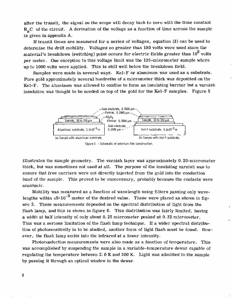
after the transit, the signal on the scope will decay back to zero with the time constant RsC of the circuit. A derivation of the voltage as a function of time across the sample is given in appendix A.
If transit times are measured for a series of voltages, equation (3) can be used to determine the dr i f t mobility. Voltages no greater than 180 volts were used since the material 's breakdown (switching) point occurs for electric fields greater than 108 volts per meter. One exception to this voltage limit was the 135-micrometer sample where up to 1000 volts were applied. This is still well below the breakdown field.
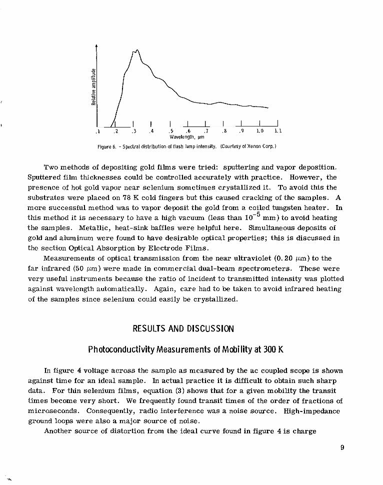
Samples were made in several ways. Kel-F or aluminum was used as a substrate. Pure gold approximately several hundreths of a micrometer thick was deposited on the Kel-F. The aluminum was allowed to oxidize to form an insulating barr ier but a varnish insulation was thought to be needed on top of the gold for the Kel-F samples. Figure 5
,-Gold electrode, 0.2000 pm-., / / / ,-Formar, 0.2000 pm.,. .\,
/ , I i ' " -I' r A l 2 O j
Sample, 10 to 150 p m I,/' Formar, 0.2000 Um,, I Sample, 10 t o EO p m \ A,-I Kel-F substrate, 1 . 6 ~ 1 0 - ~,,, m
J
(a) Sample wi th a luminum substrate. (b) Sample w i th Kel-F substrate.
Figure 5. - Schematic of selenium f i lm construct ion.
illustrates the sample geometry. The varnish layer was approximately 0.20-micrometer thick, but was sometimes not used at all. The purpose of the insulating varnish was to ensure that free car r ie rs were not directly injected from the gold into the conduction band of the sample. This proved to be unnecessary, probably because the contacts were nonohmic.
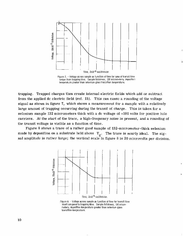
Mobility was measured as a function of wavelength using filters passing only wavelengths within *5~10-' meter of the desired value. These were placed as shown in figure 2. These measurements depended on the spectral distribution of light from the flash lamp, and this is shown in figure 6. This distribution was fairly limited, having a width at half intensity of only about 0.25 micrometer peaked at 0.32 micrometer. This was a serious limitation of the flash lamp technique. If a wider spectral distribution of photosensitivity is to be studied, another form of light flash must be found. However, the flash lamp emits into the infrared at a lower intensity.
Photoconduction measurements were also made as a function of temperature. This was accomplished by suspending the sample in a variable-temperature dewar capable of regulating the temperature between 2.0 K and 300 K. Light was admitted to the sample by passing it through an optical window in the dewar.
8
U 0)2
c-E m
F m 0)
; / I _ , Wavelength, pin
Figure 6. - Spectral distribution of flash lamp intensity. (Courtesy of Xenon Corp. )
Two methods of depositing gold films were tried: sputtering and vapor deposition. Sputtered film thicknesses could be controlled accurately with practice. However, the presence of hot gold vapor near selenium sometimes crystallized it. To avoid this the substrates were placed on 78 K cold fingers but this caused cracking of the samples. A more successful method was to vapor deposit the gold from a coiled tungsten heater. In this method it is necessary to have a high vacuum (less than mm) to avoid heating the samples. Metallic, heat-sink baffles were helpful here. Simultaneous deposits of gold and aluminum were found to have desirable optical properties; this is discussed in the section Optical Absorption by Electrode .Films.
Measurements of optical transmission from the near ultraviolet (0.20 pm) to the far infrared (50 pm) were made in commercial dual-beam spectrometers. These were very useful instruments because the ratio of incident to transmitted intensity was plotted against wavelength automatically. Again, care had to be taken to avoid infrared heating of the samples since selenium could easily be crystallized.
RESULTS AND DISCUSSION
Photoconductivity Measurements of Mobility at 300 K
In figure 4 voltage across the sample as measured by the ac coupled scope is shown against time for an ideal sample. In actual practice it is difficult to obtain such sharp data. For thin selenium films, equation (3) shows that for a given mobility the transit times become very short. We frequently found transit times of the order of fractions of microseconds. Consequently, radio interference was a noise source. High-impedance ground loops were also a major source of noise.
Another source of distortion from the ideal curve found in figure 4 is charge
9
Time, 2x10⁻⁶ secldivision
Figure 7. - Voltage across sample as funct ion of t ime for case of t rans i t t ime longer than trapping time. Sample thickness, 132 micrometers; deposition temperature greater than selenium glass t rans i t ion temperature.
trapping. Trapped charges then create internal electric fields which add or subtract from the applied dc electric field (ref. 15). This can cause a rounding of the voltage signal as shown in figure 7, which shows a measurement for a sample with a relatively large amount of trapping occurring during the transit of charge. This is taken for a selenium sample 132 micrometers thick with a dc voltage of +180 volts for positive hole carr iers . At the start of the trace, a high-frequency noise is present, and a rounding of the transit voltage is visible as a function of time.
Figure 8 shows a trace of a rather good sample of 132-micrometer-thick selenium made by deposition on a substrate held above T
g ' The trace is nearly ideal. The signal amplitude is rather large; the vertical scale in figure 8 is 20 microvolts per division. - ,
,eddiv is ion Time, 2xlO-l
Figure 8. - Voltage across sample as funct ion of t ime for t rans i t t ime shor t compared t o trapping time. Sample thickness, 132 micrometers; deposition temperature greater t han selenium glass t rans i t ion temperature.
10
a,
0 0.4400-pm f i l ter 0 No f i l ter
+I UVI
a,VIL”, ..c-
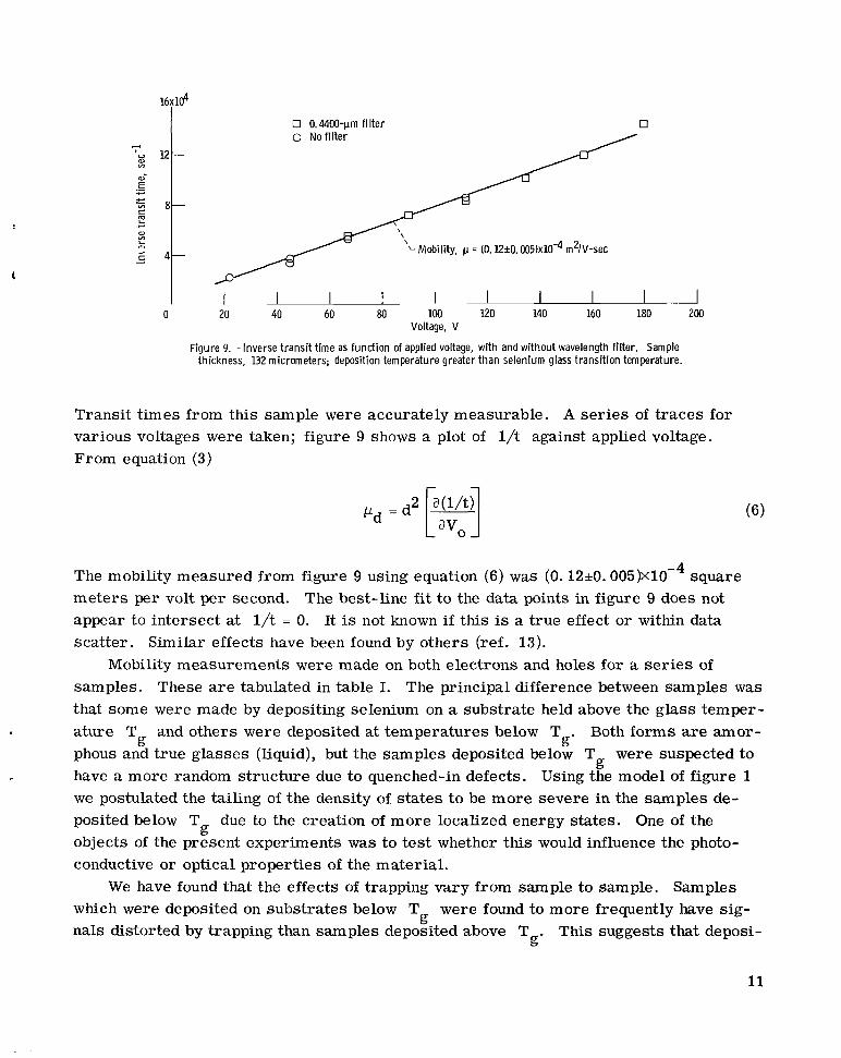
Transit times from this sample were accurately measurable. A ser ies of traces for various voltages were taken; figure 9 shows a plot of l/t against applied voltage. From equation (3)
r 1
The mobility measured from figure 9 using equation (6) was ( 0 . 1 2 ~ 0 . 0 0 5 ) ~ 1 0 - ~square meters per volt per second. The best-line f i t to the data points in figure 9 does not appear to intersect at l/t = 0. It is not known if this is a true effect or within data scatter. Similar effects have been found by others (ref. 13).
Mobility measurements were made on both electrons and holes for a ser ies of samples. These are tabulated in table I. The principal difference between samples was that some were made by depositing selenium on a substrate held above the glass temperature T
g and others were deposited at temperatures below T
g’ Both forms are amor
phous and true glasses (liquid), but the samples deposited below T were suspected to g
have a more random structure due to quenched-in defects. Using the model of figure 1 we postulated the tailing of the density of states to be more severe in the samples deposited below T due to the creation of more localized energy states. One of the gobjects of the present experiments was to test whether this would influence the photoconductive or optical properties of the material.
We have found that the effects of trapping vary from sample to sample. Samples which were deposited on substrates below T were found to more frequently have sig
gnals distorted by trapping than samples deposited above T
g’ This suggests that deposi
11
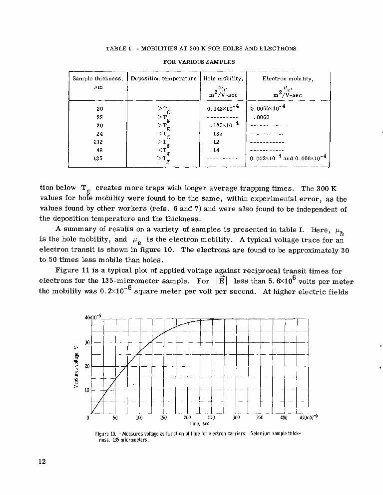
TABLE I . - MOBILITIES AT 300 K FOB HOLES AND ELECTRONS
FOR VARIOUS SAMPLES -I Sample thickness, Deposition temperati Hole mobility, Electron mobility,
20II li 135
tion below T creates more t raps with longer average trapping times. The 300 K g
values for hole mobility were found to be the same, within experimental e r ror , as the values found by other workers (refs. 6 and 7) and were also found to be independent of the deposition temperature and the thickness.
A summary of results on a variety of samples is presented in table I. Here, ph is the hole mobility, and pe is the electron mobility. A typical voltage trace for an electron transit is shown in figure 10. The electrons are found to be approximately 30 to 50 times less mobile than holes.
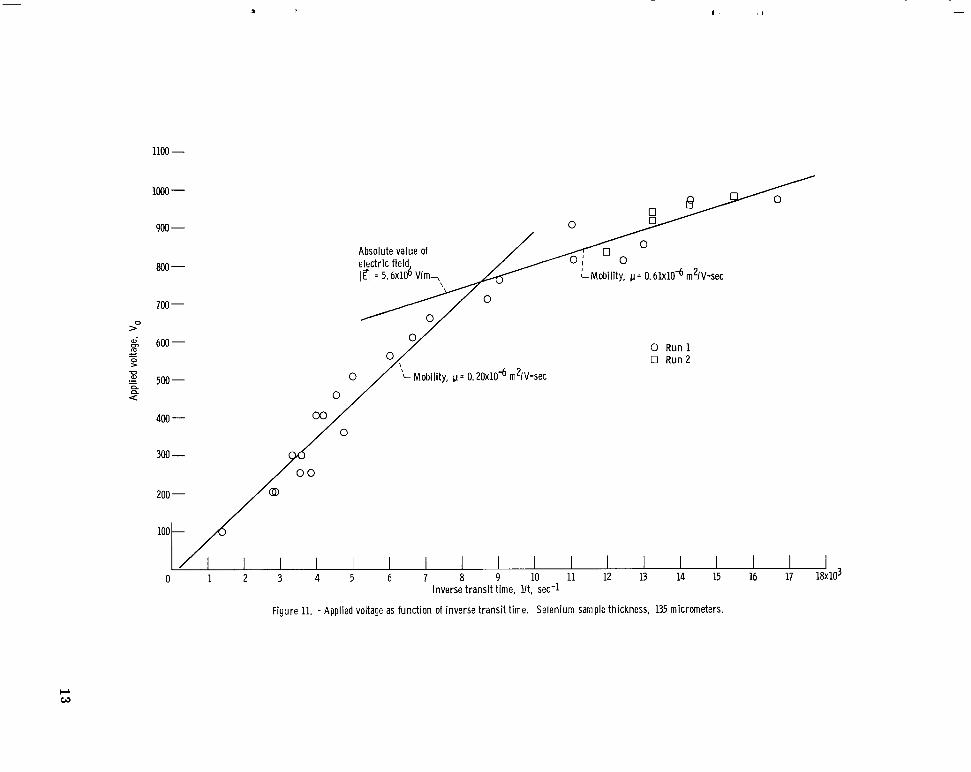
Figure 11is a typical plot of applied voltage against reciprocal transit times for electrons for the 135-micrometer sample. For I E’I l ess than 5.6X10⁶ volts per meter
the mobility was 0. 2X10⁻⁶ square meter per volt per second. At higher electric fields
Time, sec
Figure 10. -Measured voltage as funct ion of t ime for electron carr iers . Selenium sample thickness, 135 micrometers.
12
m
c1.
1 ' I
1100
loo0
900-Absolute value of
800
700 -
so % 600- 0 Run 1-I 0 0 R u n 2> '0
&' 500cz a
400
300
0 1 2 3 Inverse transit time, Ut, sec-1
Figure 11. - Applied voltage as function of inverse transit time. Selenium sample thickness, 135 micrometers.
0)
the mobility jumped by a factor of 3 to 0. 6X10⁻⁶ square meter per volt per second. The kink (abrupt change in slope in fig. 11)in the voltage against inverse transit time found for the 135-micrometer-thick sample may have been present in the 20-micrometer samples and been overlooked because of the large steps in the applied electric field. Since the samples were more mobile at higher electric fields, it appears that there is an abrupt change in the mechanism limiting mobility. Tabak and Warter (ref. 6) also found kinks but at much lower field values. Scharfe (ref. 16) has recently found an electric-field-dependent mobility in As2Se3. Lanyon and Speer (ref. 17) found kinks in current-voltage plots for selenium corresponding to the onset of space-chargelimited currents, and this may be the explanation for our observation.
Photoconduction Measurements of Mobility as Function of Temperature
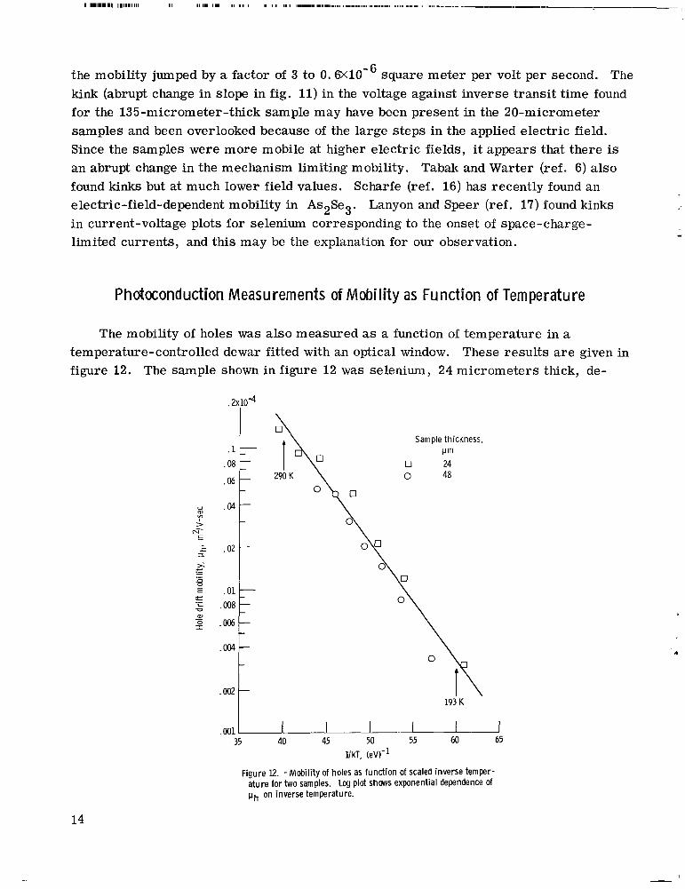
The mobility of holes was also measured as a function of temperature in a temperature-controlled dewar fitted with an optical window. These results a r e given in figure 12. The sample shown in figure 12 was selenium, 24 micrometers thick, de
.2~10-4
I d
uVI
> N-
E
S 1
Sample thickness, I m
0 24 0 48
14
posited below the glass temperature on a Kel-F substrate. The drop in mobility with temperature is exponential, following equation (5). In figure 12 the mobility in square
at 300 K to 0 . 0 0 2 9 ~ 1 0 - ~meter per volt per second varied from O . l 4 ~ l O - ~ at 190 K. The activation energy E for the mobility temperature dependence is found from the semi-log plot of the data in figure 12, and is 0.20*0.02 electron volt in the temperature range from 200 to 300 K. The difference between this value and the value of 0.14*0.01 electron volt found for samples deposited at 293 K (very near or just below T ) is signifigcant.
Grunwald and Blakney (ref. 5) found the activation energy to increase with increasing substrate temperature above T Our results suggest that the activation energy
g ' may increase for decreasing substrate temperature below T It would be worth while
g ' to examine the activation energy as a function of substrate temperature for a series of substrate temperatures below T Grunwald and Blakney (ref. 5)as well as Tabak (ref. 1) have found that above 260
g ' K the mobility is no longer exponentially dependent
on temperature. In figure 12 there a r e not enough high-temperature data to compare results.
In figure 4, below 200 K there was a significant change in the voltage-against-time plots. These no longer had kinks corresponding to well-defined transit times, instead they were exponential. It appeared that the decay times followed an exponential form,
V = Voe -tyro (7)
Where T~ is a characteristic decay time, Vo is the initial voltage, and V is the voltage after a time t'. For temperature above 160 K these time constants were well below the time constant associated with the scope (20 psec). Thus the effect was not caused by the characteristics of the measuring circuit. Another reason that the effect is not due to electronics is that T~ is very dependent on temperature, as shown in figure 12. A plot of T~ as a function of inverse temperature over the region 130 to 220 K is shown in figure 13, and implies an activation energy of 0.25*0.03 electron volt as defined by
1- a e -E/kT
7~
where T~ is a decay time constant. Tabak (ref. 1) has studied selenium (deposited above T ) in the temperature regiong
below 200 K. He did not use the same method used in the present experiments. In his experiments, well-defined transit times were found, but mobility was dependent on elect r ic field. Using electric fields of 2.lXlO6 volts per meter an activation energy of
15
Possible electronic interference-,,
Y)
------
-
_10 1 -~L
16
0.23*0.02 electron volt was found. Using an electric field of 1.5X10⁶ volts per meter, we obtained an activation energy of 0.25rtO. 03 electron volt. However, the closeness of these energy values may be fortuitous, since the two effects may o r may not be related.
The trapping time or car r ie r lifetime can be obtained from the observation of an exponential decay of signal when applied electric fields a r e small. This effect is probably not related to the decay discussed in the last paragraph. When E' is small, transit times a re longer than the time for trapping of charge. The signal then decays exponentially with a time constant characteristic of the trapping time (ref. 6). Kuninsky (ref. 8) obtained a value of 30 microseconds for the trapping time at 300 K. This is comparable to the values found in reference 5.
PhotoconductivityMeasurements of Mobility as a Function of Wavelength at 300 K
It is important for the use of amorphous semiconductors in devices to know the optical wavelengths to which samples respond. To measure this, a ser ies of optical filters was used to select wavelengths within *5. O X ~ O - ~meter of a central wavelength. Using a 132-micrometer-thick selenium sample deposited above the glass temperature, we studied the transmitted maximum signal amplitude Vmax illustrated in figure 4. In figure 14, Vmax is plotted as a function of wavelength. The figure also shows the effects of flash lamp output (fig. 6) and electrode absorption. As shown, the f lash is intense in the ultraviolet near 0.30 micrometer but cuts off near 0.20 micrometer. We were able to get a signal as low as 0.22 micrometer (ultraviolet) and as 'high as 0.60 micrometer (red light). The largest signals were found at 0.42 micrometer (blue light). In figure 14 the sudden drop in Vmax or cutoff of photoconduction beginning at 0.48 micrometer and ending at 0. 52 micrometer corresponds to a "photoconductivity edge" between 2.58 and 2. 39 electron volts.
The drop of photoresponse (Vmax) in figure 14 between 0.47 and 0.50 micrometer is a real property of the selenium and is not caused by a limitation in the f lash lamp. Between 0.50 and 0.60 micrometer the flash lamp output changes relatively little, yet the photoresponse of selenium drops off very rapidly in this region.
By using a series of filters the value of the mobility was found to be independent of wavelength to within experimental accuracy, from 0.22 to 0.55 micrometer. In figure 9 the data points using a 0.44-micrometer filter and data taken without a filter coincide. Similar results were obtained using other filters. Finding mobility independent of wavelength means that the rapid drop in Vm, near 0.50 micrometer is due to a decrease in the number of excited car r ie rs made available by optical absorption, rather than to a decrease in mobility.
17
Spectral d istr ibut ion ,-Observed maximum
Transmission of
/I
J .20 .25 .30 .35 .40 .45 .50 .55 .60
Wavelength, pm
Figure 14. - Maximum voltage (see fig. 4) across sample as func t ion of wavelength (solid curve). Cutoff between Q 4Oand Q 20 micrometer due to use of crown glass lenses. Flash lamp and gold t ransmission sketched in.
c 40
0)cn Photoconductivity w5 edge(Q4S to
L? 20 0.52 pin)-,
\
Wavelength, pm
Figure 15. - Transmission of amorphous selenium as func t ion of wavelength. Oscillations due to interference. Min imum at 35 micrometers probably excitation of a lattice vibration m d e .
18
.65
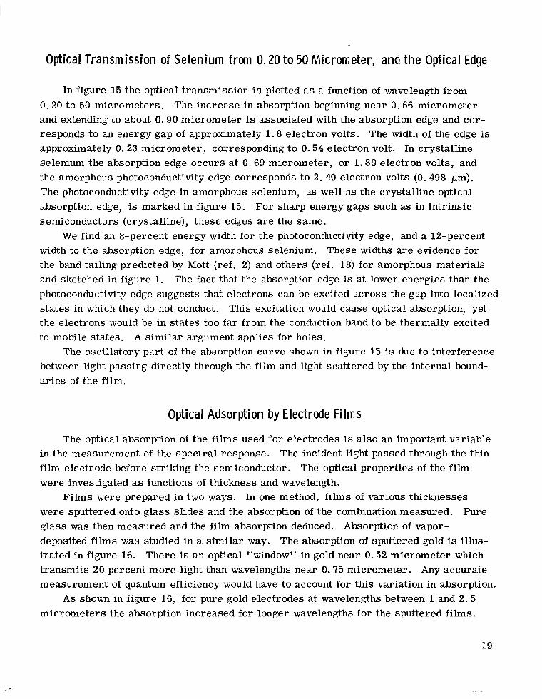
Optical Transmission of Selenium from 0.20 t o 50 Micrometer, and t h e Optical Edge
In figure 15 the optical transmission is plotted as a function of wavelength from 0.20 to 50 micrometers. The increase in absorption beginning near 0.66 micrometer and extending to about 0.90 micrometer is associated with the absorption edge and corresponds to an energy gap of approximately 1.8 electron volts. The width of the edge is approximately 0.23 micrometer, corresponding to 0.54 electron volt. In crystalline selenium the absorption edge occurs at 0.69 micrometer, or 1.80 electron volts, and the amorphous photoconductivity edge corresponds to 2.49 electron volts (0.498 p). The photoconductivity edge in amorphous selenium, as well as the crystalline optical absorption edge, is marked in figure 15. For sharp energy gaps such as in intrinsic semiconductors (crystalline), these edges are the same.
We find an 8-percent energy width for the photoconductivity edge, and a 12-percent width to the absorption edge, for amorphous selenium. These widths a re evidence for the band tailing predicted by Mott (ref. 2) and others (ref. 18) for amorphous materials and sketched in figure 1. The fact that the absorption edge is at lower energies than the photoconductivity edge suggests that electrons can be excited across the gap into localized states in which they do not conduct. This excitation would cause optical absorption, yet the electrons would be in states too far from the conduction band to be thermally excited to mobile states. A similar argument applies for holes.
The oscillatory part of the absorption curve shown in figure 15 is due to interference between light passing directly through the film and light scattered by the internal boundar ies of the film.
Optical Adsorption by Electrode Films
The optical absorption of the films used for electrodes is also an important variable The incident light passed through the thinin the measurement of the spectral response.
film electrode before striking the semiconductor. The optical properties of the film were investigated as functions of thickness and wavelength.
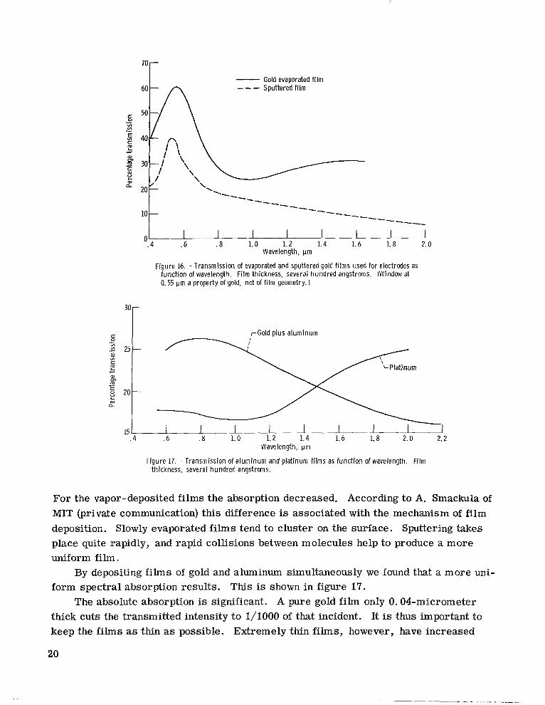
Films were prepared in two ways. In one method, films of various thicknesses were spueered onto glass slides and the absorption of the combination measured. Pure glass was then measured and the film absorption deduced. Absorption of vapor-deposited films was studied in a similar way. The absorption of sputtered gold is illustrated in figure 16. There is an optical "window" in gold near 0.52 micrometer which transmits 20 percent more light than wavelengths near 0.75 micrometer. Any accurate measurement of quantum efficiency would have to account for this variation in absorption.
As shown in figure 16, for pure gold electrodes at wavelengths between 1and 2.5 micrometers the absorption increased for longer wavelengths for the sputtered films.
19
---
m
70r Gold evaporated f i lm Sputtered f i lm
0 I I . 4 .6 .8 1.0 1.2 1.4 1.6 1.8 2.0
Wavelength, i m
Figure 16. - Transmission of evaporated and sputtered gold f i l m used for electrodes as funct ion of wavelength. Film thickness, several hundred angstroms. [Window at 0.55 pm a property of gold, not of f i lm geometry. )
r G o l d plus a luminum
m c
Q
15 .4 . 6 . a 1.0 1.2 1.4 1.6 1. a 2.0 2.2
Wavelength, pm
Figure 17. - Transmission of a luminum and plat inum f i lms as funct ion of wavelength. Film thickness, several hundred angstroms.
For the vapor-deposited films the absorption decreased. According to A. Smackula of MIT (private communication) this difference is associated with the mechanism of film deposition. Slowly evaporated films tend to cluster on the surface. Sputtering takes place quite rapidly, and rapid collisions between molecules help to produce a more uniform film.
By depositing films of gold and aluminum simultaneously we found that a more uniform spectral absorption results. This is shown in figure 17.
The absolute absorption is sigdficant. A pure gold film only 0.04-micrometer thick cuts the transmitted intensity to 1/1000 of that incident. It is thus important to keep the films as thin as possible. Extremely thin films, however, have increased
20
- ... .. .... - ...
resistance which reduces the uniformity of the electric field over the sample. Thus a compromise must be made. In practice, gold was deposited and the resistance measured. If the resistance was too high, more gold was deposited.
Mobility as a Function of Magnetic Field
An attempt was made to see whether the mobility depended on magnetic field. In metals and degenerate crystalline semiconductors, there is a strong dependence of resistance on magnetic field. In fields to 1tesla (1tesla = 10 kG), we have found that at 300 K there was no effect on hole mobility within an experimental e r r o r of rt5 percent. The reason for this is probably the low mobility or large effective mass for the selenium car r ie rs compared with metals or crystalline semiconductors. One tesla is probably much too low a magnetic field for significant effects. With at least 10 times the field strength, the chances of observing changes would be greatly improved since magnetoresistance is frequently quadratic in magnetic field (ref. 9). If changes could be observed, it would be very instructive to compare with crystalline results.
CONCLUDING REMARKS
The results of this work are pertinent to electro-optical devices, since mobility is an important parameter in their effectiveness and response speed. This report makes several contributions to understanding mobility: we have shown that the substrate deposition temperature has little effect on the mobility at 300 K. However, the temperature dependence of mobility is affected by deposition temperature. We have also shown that the 300 K electron ‘mobility tr iples by applying electric fields greater than 5x10⁶ volts per meter. Mobility is found to be independent of magnetic fields to 1 tesla within an accuracy of k5 percent. Mobility at 300 K is also shown to be independent of wavelength in the region from 0.22 to 0.60 micrometer; however, the number of car r ie rs is very dependent on wavelength, and this determines the wavelength cutoff in the number of car r ie rs excited to mobile states.
In addition, we have studied the influence of the methods of preparation of electrode films. A new phenomenon has been investigated for temperatures below 200 K, where voltage-against-time curves are exponential, rather than kinked, and the exponential decay is strongly temperature dependent.
Lewis Research Center, National Aeronautics and Space Administration,
Cleveland, Ohio, June 24, 1971, 129-02.
21
APPENDIX A
SYMBOLS
C
d
E
E
% K
k
Q
QO
RS
T
T g
t
t'
V
vO
V
X
K
I-Ld
pe
I-Lh P
capacitance
sample thickness
thermal activation energy
electric field
energygapfor amorphous materia 1s
energy gap for crystalline materials
energy gap for mobility
thickness of charge layer
Boltzmann constant
photoinjected charge
charge due to Vo
sample resistance
temperature
glass temperature
transit time
time
voltage
voltage applied across sample
drift velocity
distance
dielectric constant
drift mobility
electron drift mobility
hole drift mobility
electrical resistivity
7 trapping time
T0
decagtime
22
APPENDIX B
DERIVAT1ONS
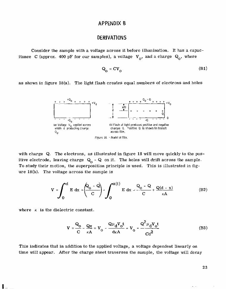
Consider the sample with a voltage across it before illumination. It has a capacitance C (approx. 400 pF for our samples), a voltage Vo, and a charge Qo, where
Qo = CVo
as shown in figure 18(a). The light flash creates equal numbers of electrons and holes
(a) Voltage Vo applied across (b)Flash of l ight produces positive and negative width d producing charge charges Q. Positive Q i s shown in transi t Q o across f i lm.
Figure 18. -Model of f i lm.
with charge Q. The electrons, as illustrated in figure 18 will move quickly to the positive electrode, leaving charge Qo - Q on it. The holes will drift across the sample. To study their motion, the superposition principle is used. This is illustrated in figure 18(b). The voltage across the sample is
V = &o - + --Q(d - x) C KA
where K is the dielectric constant.
This indicates that in addition to the applied voltage, a voltage dependent linearly on time will appear. After the charge sheet traverses the sample, the voltage will decay
23
I -
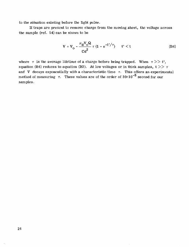
to the situation existing before the light pulse. If t raps are present to remove charge from the moving sheet, the voltage across
the sample (ref. 14) can be shown to be
v = v o -'dVoQ r ( 1 - e -t'/71 t' < t
where 7 is the average lifetime of a charge before being trapped. When T >> t', equation (B4) reduces to equation (B3). At low voltages or in thick samples, t >> 7 and V decays exponentially with a characteristic time 7. This offers an experimental method of measuring 7. These values a re of the order of 30X10-6 second for our Samples.
24
REFERENCES
1. Tabak, Mark D. : Temperature Dependence of Hole Transport in Vitreous Selenium. Phys. Rev., vol. 2B, no. 6, Sept. 15, 1970, pp. 2104-2108.
2. Mott, N. F. : Conduction and Switching in Non-Crystalline Materials. Contemp. Phys., vol. 10, Mar. 1969, pp. 125-138.
3. Fotland, Richard A. : Some Electrical Properties of Amorphous Selenium Films. J . Appl. Phys., vol. 31, no. 9, Sept. 1960, pp. 1558-1565.
4. Hartke, J. L.: Drift Mobilities of Electrons and Holes and Space-Charge-Limited Currents in Amorphous Selenium Films. Phys. Rev. , vol. 125, no. 4, Feb. 15, 1962, pp. 1177-1192.
5 . Grunwald, H. P. ; and Blakney, R. M. : Electron and Hole Drift Mobilities in Vitreous Selenium. Phys. Rev. , vol. 165, no. 3, Jan. 15, 1968, pp. 1006-1010.
6. Tabak, Mark D.; and Warter, Peter J. , Jr. : Field-Controlled Photogeneration and Free-Carrier Transport in Amorphous Selenium Films. Phys. Rev., vol. 173, no. 3, Sept. 15, 1968, pp. 899-907.
7. Spear, Walter E.: Drift Mobility Techniques for the Study of Electrical Transport Properties in Insulating Solids. J. Non-Cryst. Solids, vol. 1, no. 3, Apr. 1969, pp. 197-214.
8. Kuninsky, M. : Photoconductivity in Thin Films of Amorphous Selenium. M. S. Thesis, Massachusetts Inst. Tech., 1970.
9. Ziman, J. M.: Electrons and Phonons. Clarendon Press, 1960.
10. Blakemore, John S.: Semiconductor Statistics. Pergamon Press, 1962.
11. Cohen, Morrel H. : Review of the Theory of Amorphous Semiconductors. J. Non-Cryst. Solids, vol. 4, no. 1, Apr. 1970, pp. 391-409.
12. Stuke, J. : Review of Optical and Electrical Properties of Amorphous Semiconductors . J. Non-Cryst. Solids, vol. 4, no. 1, Apr. 1970, pp. 1-26.
13. Tauc, J. ; Menth, A. ; and Wood, D. L. : Optical and Magnetic Investigations of the Localized States in Semiconducting Glasses. Phys. Rev. Letters, vol. 25, no. 11, Sept. 14, 1970, pp. 749-752.
14. Scharfe, Merlin E.; and Tabak, Mark D. : Bulk Space Charge and Transient Photoconductivity in Amorphous Selenium. J. Appl. Phys. , vol. 40, no. 8, July 1969, pp. 3230-3237.
25
15. Kaplow, Roy; Rowe, T. A. ; and Averbach, B. L. : Atomic Arrangement in Vitreous Selenium. Phys. Rev., vol. 168, no. 3, Apr. 15, 1968, pp. 1068-1079.
16. Scharfe, M. : Transient Photoconductivity in Vitreous As2Se3. Phys. Rev., vol. 2, no. 12, Dec. 15, 1970, pp. 5025-5035.
17. Lanyon, H. P. D. ; and Spear, W. E. : Space Charge Limited Current Flow and Deep Trapping in Selenium. Proc. Phys. SOC. (London), vol. 77, pt. 6, June 1961, pp. 1157-1165.
18. Cohen, Morrel H. ; Fritzsche, H. ; and Ovshinsky, S. R. : Simple Band Model for Amorphous Semiconducting Alloys. Phys. Rev. Letters, vol. 22, no. 20, May 19, 1969, pp. 1065-1068.
26 NASA-Langley, 1971 -26 E-6302
N A T I O N A L A E R O N A U T I C S A N D SPACE A D M I S T R A T I O N W A S H I N G T O N , D.C. 20546
POSTAGE AND FEES PAID NATIONAL AERONAUTICS A N D
O F F I C I A L B U S I N E S S FIRST CLASS MAIL SPACE ADMINISTRATION (S)PENALTY FOR PRIVATE USE $300 USMAIL
025 001 C1 U 2 5 710910 S00903DS DEPT OF THE A I R FORCE AF SPSTEBS COMFIAND AF UEAPONS L A B (RLOE) ATTN: E LOU BOWMAHS CEiIEP TECH L I B R A R Y K I B T L A N D AFB NH 87117
If Undeliverable (Section 158 ’ Postal Manual) Do Nor Return
“The aeronautical and space activities of the United Stntes shall be conducted so as to contribute . . . to the expansion of human knowledge of phenomena in the atmosphere and space. The Administration shall provide for the widest practicable and appropriate dissemination of inforination concerning its actitdies and the results thereof.”
-NATIONALAERONAUTICSAND SPACE ACTOF 1958
NASA SCIENTIFIC AND TECHNICAL PUBLICATIONS
TECHNICAL REPORTS: Scientific and technical information considered important, complete, and a lasting contribution to existing knowledge.
TECHNICAL NOTES: Information less broad in scope but nevertheless of importance as a contribution to existing knowledge.
TECHNICAL MEMORANDUMS: Information receiving limited distribution because of preliminary data, security classification, or other reasons.
CONTRACTOR REPORTS: Scientific and technical information generated under a NASA contract or grant and considered an important contribution to existing knowledge.
TECHNICAL TRANSLATIONS: Information published in a foreign language considered to merit NASA distribution in English.
SPECIAL PUBLICATIONS: Information derived from or of value to NASA activities. Publications include conference proceedings, monographs, data compilations, handbooks, sourcebooks, and special bibliographies.
TECHNOLOGY UTILIZATION PUBLICATIONS: Information on technology used by NASA that may be of particular interest in commercial and other non-aerospace applications. Publications include Tech Briefs, Technology Utilization Reports and Technology Surveys.
Details on the availability of these publications may be obtained from:
SCIENTIFIC AND TECHNICAL INFORMATION OFFICE
NATIONAL AERONAUTICS AND SPACE ADMINISTRATION Washington, D.C. PO546
1