photolithography machine control system ben conrad and mark edwards projects in computer engineering...
Post on 19-Dec-2015
214 views
TRANSCRIPT
Photolithography Machine Control System
Ben Conrad and Mark EdwardsProjects in Computer
Engineering IIDecember 9, 2003
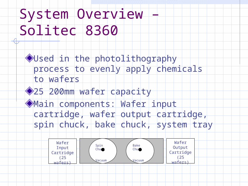
System Overview – Solitec 8360
Used in the photolithography process to evenly apply chemicals to wafers25 200mm wafer capacityMain components: Wafer input cartridge, wafer output cartridge, spin chuck, bake chuck, system tray
Spin Chuck Vacuum Tube
Bake Chuck Vacuum Tube
Wafer Output Cartridge
(25 wafers)
Wafer Input Cartridge
(25 wafers)
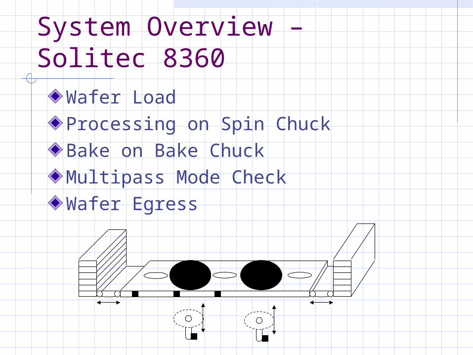
System Overview – Solitec 8360
Wafer Load
Processing on Spin Chuck Bake on Bake ChuckMultipass Mode CheckWafer Egress
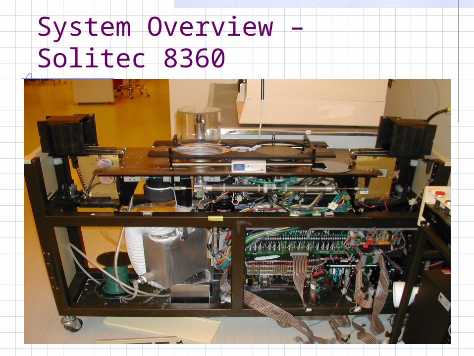
System Overview – Solitec 8360
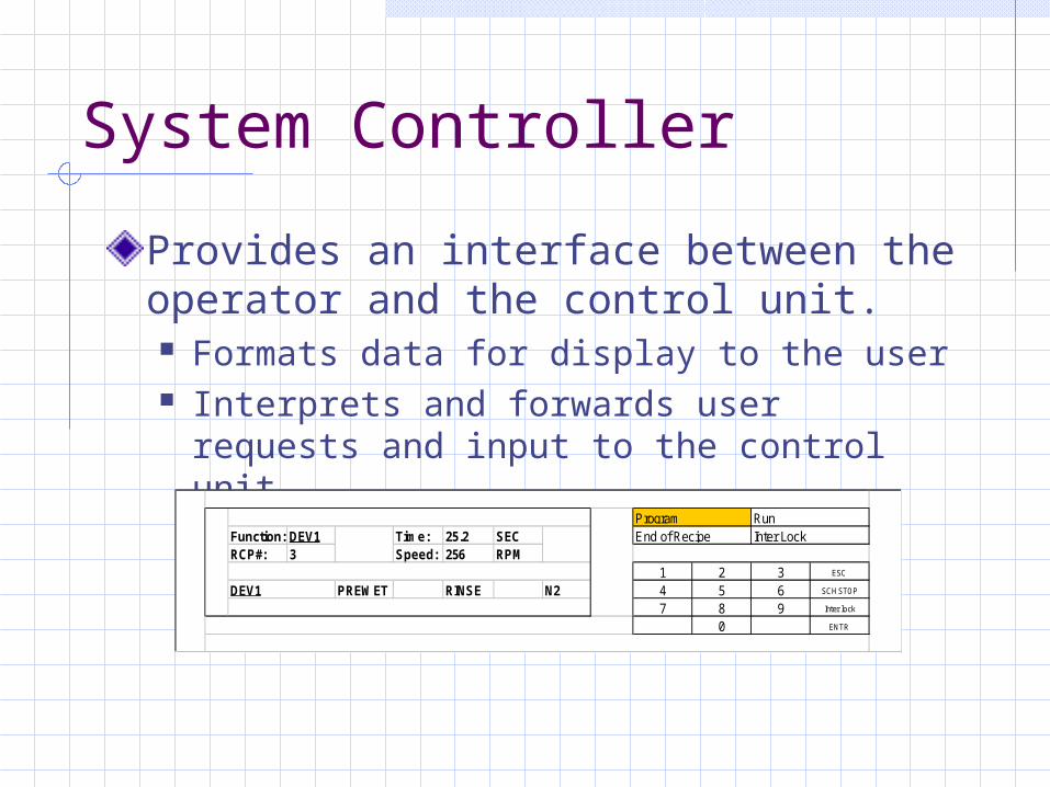
System Controller
Provides an interface between the operator and the control unit. Formats data for display to the user Interprets and forwards user requests and
input to the control unit
Function: DEV1 Time: 25.2 SECRCP#: 3 Speed: 256 RPM
1 2 3 ESC
PREWET RINSE N2 4 5 6 SCH STOP
7 8 9 Inter lock
0 ENTR
Program RunEnd of Recipe Inter Lock
DEV1
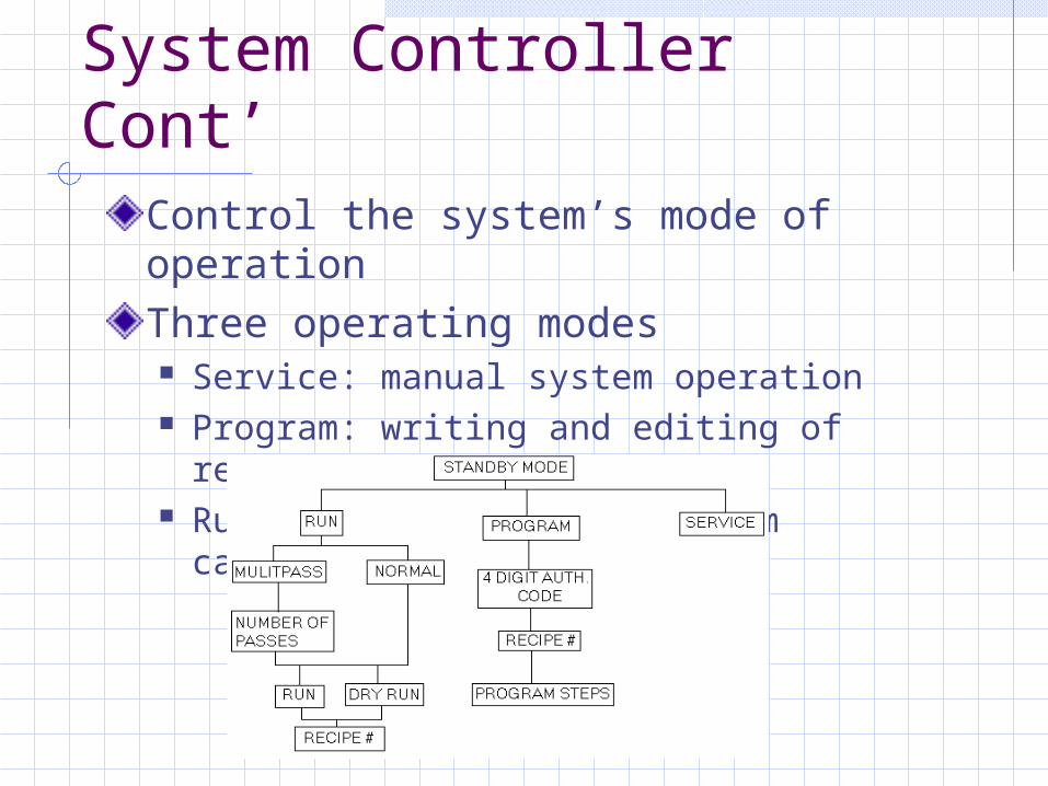
System Controller Cont’Control the system’s mode of operationThree operating modes Service: manual system operation Program: writing and editing of recipes Run: recipe execution/system calibration
Recipe Commands
Seven Executable Commands PREWET: Dispense de-ionized(DI) water Dispense DEV#1: Dispense developer solution RINSE: Dispenses DI water to clean wafer N2: Dispenses Stream of Nitrogen (N2) SPIN: Spin Dry the wafer WAIT: Static delay option.
Parameters Time: .1 – 999.9 sec. (.1 second resolution) Speed: 0-7,999 RPM Ramp: 0 – 40 KRPM/s
Motivation
Old controller was corroded; less elements in our design -> more reliableCost savings to customer, Dr. Raisanen, associate director of RIT’s fabOur design ~$350, vs. $3k-$15k
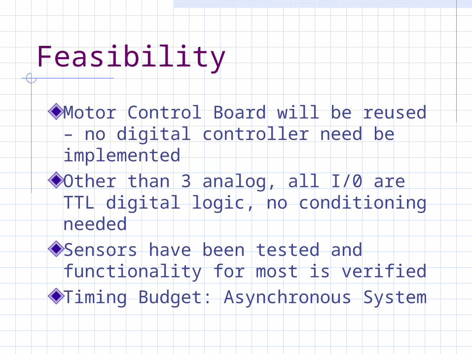
Feasibility
Motor Control Board will be reused – no digital controller need be implementedOther than 3 analog, all I/0 are TTL digital logic, no conditioning neededSensors have been tested and functionality for most is verifiedTiming Budget: Asynchronous System
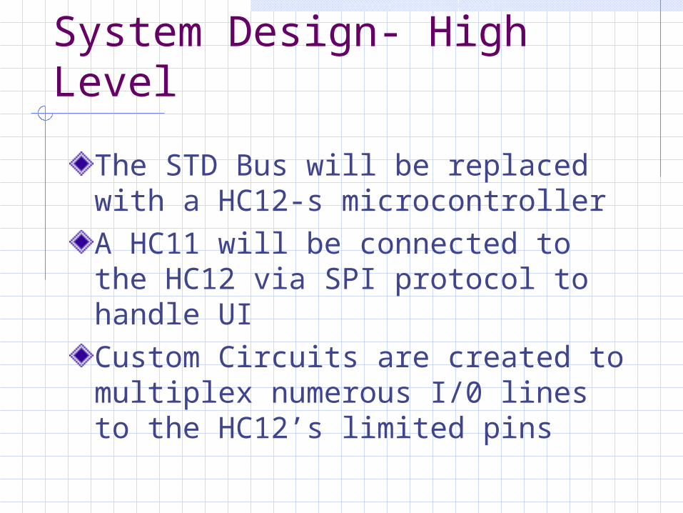
System Design- High Level
The STD Bus will be replaced with a HC12-s microcontrollerA HC11 will be connected to the HC12 via SPI protocol to handle UICustom Circuits are created to multiplex numerous I/0 lines to the HC12’s limited pins
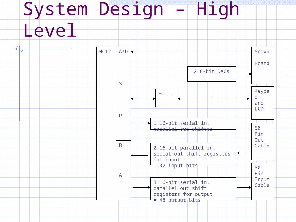
System Design – High Level
HC12
A
B
P
S
A/D
50 PinInput Cable
50 PinOut Cable
KeypadandLCD
Servo Board
3 16-bit serial in, parallel out shift registers for output= 48 output bits
2 16-bit parallel in, serial out shift registers for input= 32 input bits
1 16-bit serial in, parallel out shifter
2 8-bit DACs
HC 11
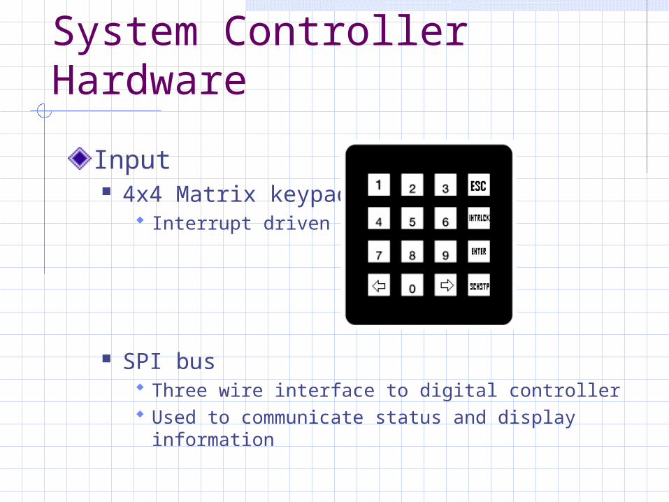
System Controller Hardware
Input 4x4 Matrix keypad
Interrupt driven
SPI bus Three wire interface to digital controller Used to communicate status and display
information
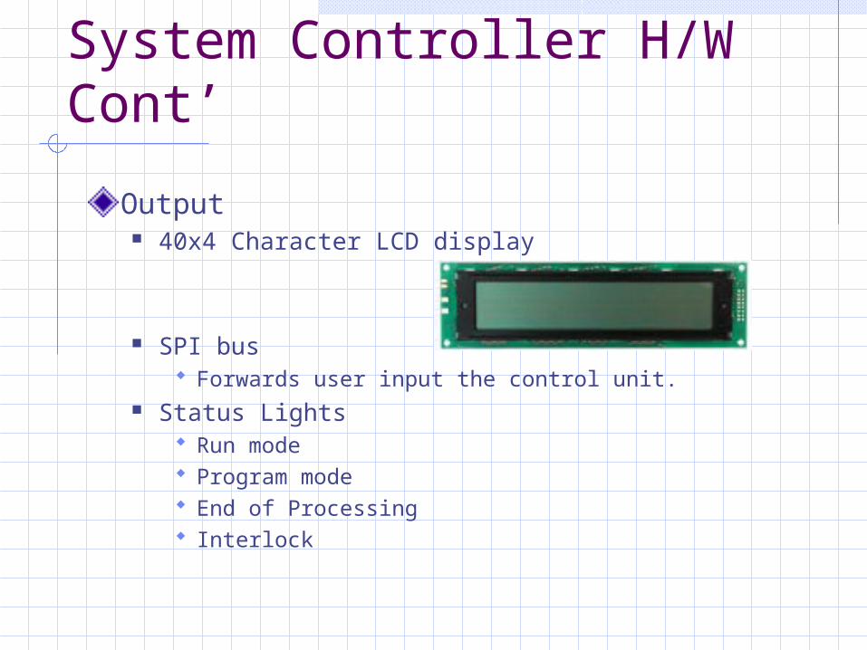
System Controller H/W Cont’
Output 40x4 Character LCD display
SPI bus Forwards user input the control unit.
Status Lights Run mode Program mode End of Processing Interlock
System Controller H/W Cont’
Processing unit Motorola 68HC11
512 bytes RAM, 512 bytes EEPROM Synchronous peripheral interface (SPI) Real time interrupt circuit
Data aggregation Distribute workload
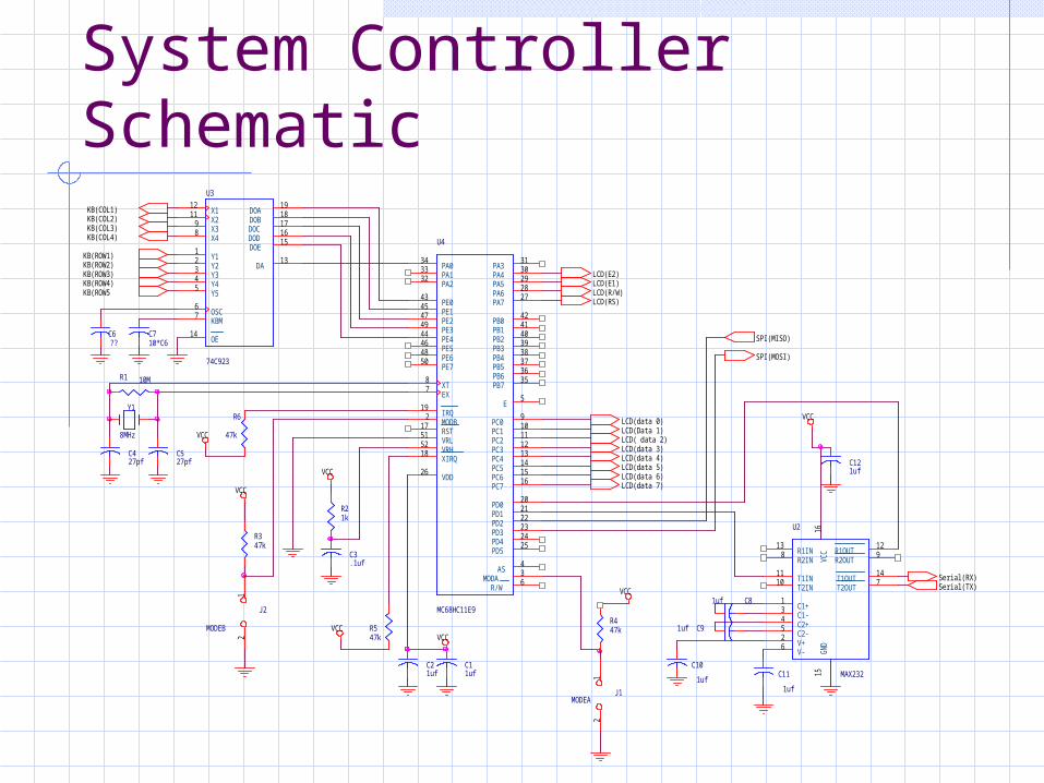
System Controller Schematic
KB(ROW1)
C10
1uf
C121uf
KB(ROW4)
VCC
KB(COL2)
VCC
C6??
R347k
C11uf
LCD( data 2)
Serial(RX)
VCC
LCD(data 4)C527pf
LCD(data 7)
R547k
C11
1uf
LCD(RS)
LCD(E2)
C91uf
KB(ROW3)
SPI(MOSI)
J2
MODEB
12
U4
MC68HC11E9
5251
3130292827
4241403938373635
910111213141516
202122232425
5
26
87
17
19
18
2
343332
4345474944464850
436
VRHVRL
PA3PA4PA5PA6PA7
PB0PB1PB2PB3PB4PB5PB6PB7
PC0PC1PC2PC3PC4PC5PC6PC7
PD0PD1PD2PD3PD4PD5
E
VDD
XTEX
RST
IRQ
XIRQ
MODB
PA0PA1PA2
PE0PE1PE2PE3PE4PE5PE6PE7
ASMODA
R/W
KB(COL1)
KB(COL4)
LCD(Data 1)
C710*C6
LCD(data 6)
U2
MAX232
1345
1615
26
129
1110
138
147
C1+C1-C2+C2-
VC
CG
NDV+
V-
R1OUTR2OUT
T1INT2IN
R1INR2IN
T1OUTT2OUT
LCD(E1)
VCC
SPI(MISO)
C81uf
R447k
Y1
8MHz
C21uf
KB(ROW2)
J1MODEA
12
R21k
R1 10M
KB(ROW5
LCD(data 3)
KB(COL3)
C3.1uf
VCC
C427pf
LCD(data 5)
LCD(data 0)
VCC
LCD(R/W)
Serial(TX)
R6
47k
U3
74C923
67
14
1918171615
1312345
1211
98
OSCKBM
OE
DOADOBDOCDODDOE
DAY1Y2Y3Y4Y5
X1X2X3X4
VCC
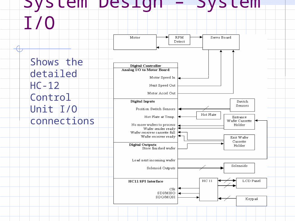
System Design – System I/O
Shows the detailed HC-12 Control Unit I/O connections
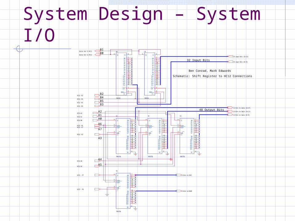
System Design – System I/O
B0
HC12- A3
B1
16 Bits to Cable (16-31)
8 Bits to DAC1
A4
Serial Out to HC12
B2
HC12- B4
U5
74F676
4
5
2
6
1
78910111314151617181920212223
SI
MODE
CLK
SO
CS
P0P1P2P3P4P5P6P7P8P9
P10P11P12P13P14P15
HC12-A116 Bits to Cable (0-15)
HC12- B2
B3
HC12- A7
8 Bits to DAC0
B4
Serial Out to HC12
B5
HC12-A2
HC12-A5
U3
74F675A
4
3
5
7891011131415
1617181920212223
6
1
2
SI
R/W
STCP
Q0Q1Q2Q3Q4Q5Q6Q7
Q8Q9
Q10Q11Q12Q13Q14Q15
SO
CS
SHCP
Ben Conrad, Mark Edwards
A3
A6
Schematic: Shift Register to HC12 Connections
16 input Bits (0-15)
HC12- A6
32 Input Bits
A7
U2
74F675A
4
3
5
7891011131415
1617181920212223
6
1
2
SI
R/W
STCP
Q0Q1Q2Q3Q4Q5Q6Q7
Q8Q9
Q10Q11Q12Q13Q14Q15
SO
CS
SHCP
U2
74F675A
4
3
5
7891011131415
1617181920212223
6
1
2
SI
R/W
STCP
Q0Q1Q2Q3Q4Q5Q6Q7
Q8Q9
Q10Q11Q12Q13Q14Q15
SO
CS
SHCP
HC12-A4
16 input Bits (16-31)
A2
HC12- B3
A1
U6
74F676
4
5
2
6
1
78910111314151617181920212223
SI
MODE
CLK
SO
CS
P0P1P2P3P4P5P6P7P8P9
P10P11P12P13P14P15
HC12-A0A0
U2
74F675A
4
3
5
7891011131415
1617181920212223
6
1
2
SI
R/W
STCP
Q0Q1Q2Q3Q4Q5Q6Q7
Q8Q9
Q10Q11Q12Q13Q14Q15
SO
CS
SHCP
HC12- B5
HC12 - P7
16 Bits to Cable (32-47)
HC12 - P6
48 Output Bits
A5
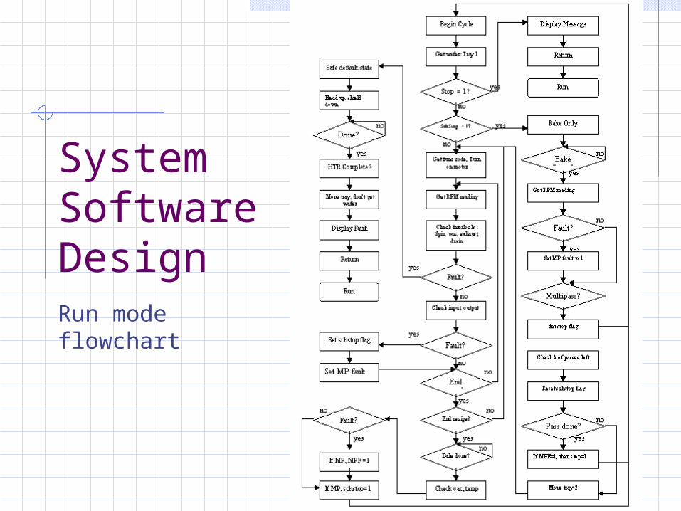
System Software DesignRun mode flowchart
System Software Design
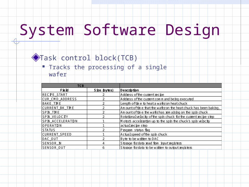
Task control block(TCB) Tracks the processing of a single wafer
Field Size (bytes) DescriptionRECIPE_START 2 Address of the current recipeCUR_CMD_ADDRESS 2 Address of the current command being executedBAKE_TIME 2 Length of time to heat a wafer on heat chuckCURRENT_BK_TIME 2 Amount of time that the wafer on the heat chuck has been baking. SPIN_TIME 2 Amount of time the wafer has remaining on the spin chuckSPIN_VELOCITY 2 Rotational velocity of the spin chuck for the current recipe stepSPIN_ACCELERATION 1 Motor's acceleration up to the spin the chuck's spin velocityOPERATION 1 actual recipe stepSTATUS 2 Program status flagCURRENT_SPEED 1 Actual speed of the spin chuckDAC_OUT 2 Byte to be written to DACSENSOR_IN 4 Storage for data read from input registersSENSOR_OUT 6 Storage for data to be written to output registers
TCB
Already Completed
Parts ordered and receivedHardware schematicsSoftware flowchartsTask control designSensor/System tests
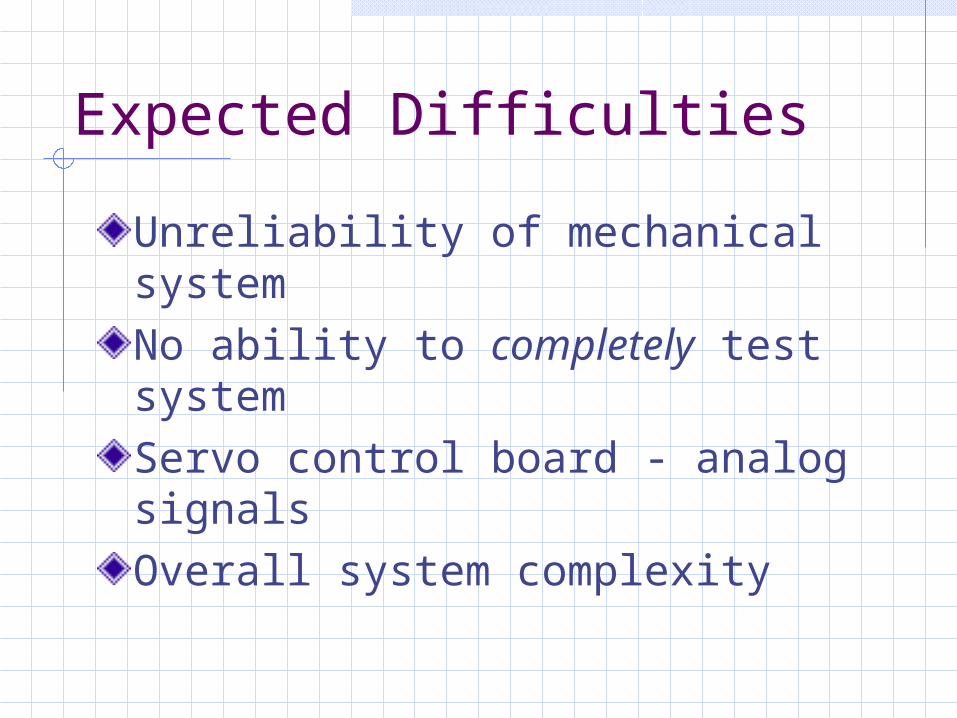
Expected Difficulties
Unreliability of mechanical systemNo ability to completely test systemServo control board - analog signalsOverall system complexity