photonic dispersive delay line for broadband microwave signal processing · · 2017-11-19photonic...
TRANSCRIPT

Photonic Dispersive Delay Line for Broadband
Microwave Signal Processing
Jiejun Zhang
Thesis submitted to the Faculty of Graduate
and Postdoctoral Studies in partial
fulfillment of the requirements for a doctoral
degree in Electrical and Computer
Engineering
School of Electrical Engineering and Computer Science
Faculty of Engineering
University of Ottawa
© Jiejun Zhang, Ottawa, Canada, 2017
ii
ACKNOWLEDGEMENTS
First, I would like to express my greatest gratitude to my supervisor, Prof. Jianping
Yao, for constantly providing valuable guidance and advices during my four-year PhD
study. Without his support, this work would never be possible. He has inspired me with his
dedication and passion for doing research, which will be beneficial for me for lifelong.
Special thanks for Prof. Lawrence Chen from McGill University, Prof. Jacques
Albert from Carleton University and Prof. Bahram Jalali from the University of California,
Los Angeles, for their inspiring discussions for my PhD project, and also Prof. Qizhen Sun,
my Master supervisor at Huazhong University of Science and Technology, China, for
providing continuous suggestion and encouragement after I graduated.
I would also like to sincerely thank all my colleagues in the Microwave Photonics
Research Laboratory at the University of Ottawa, who have given me enormous help both
inside and outside the lab since my first day in Ottawa. They are Wangzhe Li, Weilin Liu,
Weifeng Zhang, Olympio L. Coutinho, Hiva Shahoei, Fanqi Kong, Xiang Chen, Yiping
Wang, Dan Zhu, Bruno Romeira, Liang Gao, Tong Shao, Muguang Wang, Wentao Cui,
Honglei Guo, Fangjian Xing and Nasrin Ehteshami.
Finally, I appreciate the love and support from my family. It is the love of my parents
and my two beautiful sisters that drives me this far in the pursuit of knowledge.

iii
ABSTRACT
The development of communications technologies has led to an ever-increasing
requirement for a wider bandwidth of microwave signal processing systems. To overcome
the inherent electronic speed limitations, photonic techniques have been developed for the
processing of ultra-broadband microwave signals. A dispersive delay line (DDL) is able to
introduce different time delays to different spectral components, which are used to
implement signal processing functions, such as time reversal, time delay, dispersion
compensation, Fourier transformation and pulse compression. An electrical DDL is usually
implemented based on a surface acoustic wave (SAW) device or a synthesized C-sections
microwave transmission line, with a bandwidth limited to a few GHz. However, an optical
DDL can have a much wider bandwidth up to several THz. Hence, an optical DDL can be
used for the processing of an ultra-broadband microwave signal. In this thesis, we will
focus on using a DDL based on a linearly chirped fiber Bragg grating (LCFBG) for the
processing of broadband microwave signals. Several signal processing functions are
investigated in this thesis. 1) A broadband and precise microwave time reversal system
using an LCFBG-based DDL is investigated. By working in conjunction with a
polarization beam splitter, a wideband microwave waveform modulated on an optical pulse
can be temporally reversed after the optical pulse is reflected by the LCFBG for three times
thanks to the opposite dispersion coefficient of the LCFBG when the optical pulse is
reflected from the opposite ends. A theoretical bandwidth as large as 273 GHz can be
achieved for the time reversal. 2) Based on the microwave time reversal using an LCFBG-
based DDL, a microwave photonic matched filter is implemented for simultaneously

iv
generating and compressing an arbitrary microwave waveform. A temporal convolution
system for the calculation of real time convolution of two wideband microwave signals is
demonstrated for the first time. 3) The dispersion of an LCFBG is determined by its
physical length. To have a large dispersion coefficient while maintaining a short physical
length, we can use an optical recirculating loop incorporating an LCFBG. By allowing a
microwave waveform to travel in the recirculating loop multiple times, the microwave
waveform will be dispersed by the LCFBG multiple times, and the equivalent dispersion
will be multiple times as large as that of a single LCFBG. Based on this concept, a time-
stretch microwave sampling system with a record stretching factor of 32 is developed.
Thanks to the ultra-large dispersion, the system can be used for single-shot sampling of a
signal with a bandwidth up to a THz. The study in using the recirculating loop for the
stretching of a microwave waveform with a large stretching factor is also performed. 4)
Based on the dispersive loop with an extremely large dispersion, a photonic microwave
arbitrary waveform generation system is demonstrated with an increased the time-
bandwidth product (TBWP). The dispersive loop is also used to achieve tunable time
delays by controlling the number of round trips for the implementation of a photonic true
time delay beamforming system.

v
TABLE OF CONTENTS
ACKNOWLEDGEMENTS ................................................................................................ II
ABSTRACT ....................................................................................................................... III
TABLE OF CONTENTS .................................................................................................... V
LIST OF FIGURES ....................................................................................................... VIII
LIST OF ACRONYMS .................................................................................................. XIV
CHAPTER 1 INTRODUCTION .................................................................................... 1
1.1 Background Review ........................................................................................................................... 1
1.2 Major Contributions of This Thesis ................................................................................................. 7
1.3 Organization of This Thesis .............................................................................................................. 9
CHAPTER 2 SIGNAL PROCESSING BASED ON A DISPERSIVE DELAY LINE
.................................................................................................................. 11
2.1 Fiber Bragg Gratings Based Delay Lines ....................................................................................... 11
2.1.1 FBG basics .............................................................................................................................. 12
2.1.2 LCFBG and dispersive loop .................................................................................................... 14
2.2 Signal Processing Based on a Single LCFBG................................................................................. 17
2.2.1 Time reversal ........................................................................................................................... 17
2.2.2 Pulse compression ................................................................................................................... 19
2.2.3 Temporal convolution ............................................................................................................. 26
2.3 Single Processing Based on a Dispersive Loop .............................................................................. 27
2.3.1 Time-stretched sampling ......................................................................................................... 28
2.3.2 Large time-bandwidth product signal generation .................................................................... 31
2.3.3 True-time delay beamforming ................................................................................................. 35
2.4 Summary ........................................................................................................................................... 40
CHAPTER 3 MICROWAVE TIME REVERSAL ..................................................... 41
3.1 Operation Principle .......................................................................................................................... 42
3.1.1 System architecture ................................................................................................................. 42
3.1.2 Time reversal modeling ........................................................................................................... 44

vi
3.1.3 Waveform distortion ............................................................................................................... 47
3.1.4 Electrical and optical bandwidth limit ..................................................................................... 49
3.2 Experimental Implementation ........................................................................................................ 53
3.3 Performance Evaluation .................................................................................................................. 55
3.4 Conclusion......................................................................................................................................... 57
CHAPTER 4 ARBITRARY WAVEFORM GENERATION AND PULSE
COMPRESSION ............................................................................................. 58
4.1 Operation Principle .......................................................................................................................... 59
4.2 Theoretical Analysis ......................................................................................................................... 61
4.3 Experimental Evaluation ................................................................................................................. 64
5.4 Conclusion......................................................................................................................................... 69
CHAPTER 5 TEMPORAL CONVOLUTION OF MICROWAVE SIGNALS ...... 71
5.1 Convolution Basics ........................................................................................................................... 71
5.2 Experimental Implementation ........................................................................................................ 73
5.3 Experimental Evaluation ................................................................................................................. 81
5.4 Conclusion......................................................................................................................................... 86
CHAPTER 6 TIME STRETCHED SAMPLING BASED ON A DISPERSIVE
LOOP ................................................................................................................ 88
6.1 Operation Principle .......................................................................................................................... 89
6.2 Experimental Implementation ........................................................................................................ 92
6.2 Experimental Results ....................................................................................................................... 94
6.3 Conclusion......................................................................................................................................... 99
CHAPTER 7 LINEARLY CHIRPED MICROWAVE WAVEFORM
GENERATION .............................................................................................. 100
7.1 Operation Principle ........................................................................................................................ 101
7.2 Experimental Implementation ...................................................................................................... 106
7.3 Experimental Results ..................................................................................................................... 109
7.4 Conclusion....................................................................................................................................... 114
CHAPTER 8 PHOTONIC TRUE-TIME DELAY BEAMFORMING .................. 115
8.1 Photonic True-Time Delay Based on a Dispersive Loop............................................................. 116
8.2 Experimental Implementation ...................................................................................................... 120

vii
8.3 Performance Evaluation ................................................................................................................ 123
8.4 Discussion and Conclusion ............................................................................................................ 128
CHAPTER 9 SUMMARY AND FUTURE WORK ................................................. 131
6.1 Summary ......................................................................................................................................... 131
6.2 Future work .................................................................................................................................... 133
REFERENCES ................................................................................................................. 135
PUBLICATIONS ............................................................................................................. 147
Journal Papers: .................................................................................................................................... 147
Conference Papers: .............................................................................................................................. 150
viii
LIST OF FIGURES
Fig. 1.1 Block diagram of a microwave photonic system to generate a time delay to a microwave signal using
an optical delay line. TLS: tunable laser source; PD: photodetector. ....................................................... 4
Fig. 2.1 FBG fabrication based on the phase mask technique. ......................................................................... 12
Fig. 2.2 The illustration for the operation of a uniform FBG. .......................................................................... 13
Fig. 2.3 The simulated spectral response of a uniform FBG. (a) Amplitude response; (b) group delay response.
................................................................................................................................................................ 14
Fig. 2.4 The illustration for the operation of an LCFBG. ................................................................................. 15
Fig. 2.5 The simulated spectral response of an LCFBG. (a) Amplitude response; (b) group delay response. . 15
Fig. 2.6 (a) A dispersive fiber recirculating loop incorporating an LCFBG to achieve a large time delay tuning
range; (b) the group delay response of the loop when a pulse recirculates in the loop for different
number of round trips controlled by the 2×2 switch. .............................................................................. 17
Fig. 2.7 (a) Waveform and (b) spectrogram of the LCMW used in the simulation. ........................................ 22
Fig. 2.8 The frequency response of the designed matched filter: (a) magnitude; (b) group delay. .................. 22
Fig. 2.9 The compressed pulse with a pulse width of 4.8 ns. ........................................................................... 23
Fig. 2.10 The 16-bit pseudorandom binary phase coded signal (blue) and the phase code (red × ). ............. 24
Fig. 2.11 The waveform achieved by compressing the phase coded waveform using cross-correlation
technique. ............................................................................................................................................... 24
Fig. 2.12 Phased array antenna for beamforming. ........................................................................................... 37
Fig. 2.13 (a) Beam pattern with phase shifter steering; (b) beam pattern with time delay beam forming. In the
simulation: N=40; d=1.5 cm; f0=10 GHz. ............................................................................................... 38
Fig. 3.1 Schematic of the proposed microwave time reversal system. MLL: mode-locked laser; OF: optical
filter; LCFBG: linearly chirped fiber Bragg grating; PC: polarization controller; MZM: Mach-Zehnder
modulator; PBS: polarization beam splitter; PD: photodetector; OC: optical circulator. ....................... 43
Fig. 3.2 The reflection spectrum and group delay responses of the LCFBG. .................................................. 45
Fig. 3.3 The implementation of the proposed microwave time reversal system using three LCFBGs. ........... 45

ix
Fig. 3.4 The simulated time reversed waveform considering the impact from 2 /G t . Dotted: input up-
chirped waveform; dash: time-reversed output waveform with a frequency down-chip; solid: the profile
of 2 /G t , determined by the spectrum of the optical pulse from the MLL and the dispersion of
the LCFBG. ............................................................................................................................................ 49
Fig. 3.5 The simulated time reversed waveform when the limited bandwidth of the electronic components is
considered. Solid: input chirped signal; dash: output time-reversed signal for a limited electronic
bandwidth of 4 GHz. .............................................................................................................................. 50
Fig. 3.6 The mechanism for the bandwidth limit of the optical part. (a) Optical carrier c and sidebands
reflected by the LCFBG. As modulation frequency increases from 1 to 3, the sidebands may locate
outside the reflection band of LCFBG; (b) the corresponding frequency response of the LCFBG. ....... 52
Fig. 3.7 Microwave spectral response of the time reversal system due to the finite bandwidth of the LCFBG.
................................................................................................................................................................ 53
Fig. 3.8 Photograph of the experiment setup. Two 3-port circulators are cascaded to function as a 4-port
circulator OC2. ....................................................................................................................................... 54
Fig. 3.9 Comparison between the original and the time reversed waveforms. (a) sawtooth wave; (b) chirped
wave; (c) arbitrary waveform. The corresponding correlation coefficients are calculated to be 0.930,
0.939, 0.951. ........................................................................................................................................... 57
Fig. 4.1 Schematic diagram of the microwave photonic signal processor. MPF: microwave photonic filter;
TRM: time reversal module; BOS: broadband optical source; C1, C2: 3-dB optical couplers; WS:
waveshaper; TDL: tunable delay line; MZM: Mach-Zehnder modulator; Rx: receiving antenna; MC:
microwave combiner; OC: optical circulator; LCFBG: linearly chirped fiber Bragg grating; PD:
photodetector; EDFA: erbium doped fiber amplifier; PC: polarization controller; PBC: polarization
beam combiner; PG: pulse generator; Tx: transmitting antenna. ............................................................ 61
Fig. 4.2 The spectrum of the optical carrier measured at the output of the MZI when a quadratic phase is
applied to the WS. .................................................................................................................................. 65
Fig. 4.3 The magnitude and group delay response of the MPF when a quadratic phase is applied to the WS. 66

x
Fig. 4.4 (a) The LCMW generated at the output of PD2 with the TRM connected when a short pulse is
applied to the MZM. (b) The signal at the output of PD1. The LCMW is highly compressed. (c) The
LCMW at the output of PD2 with the TRM disconnected. (d) The signal at the output of PD1. No pulse
compression is observed. ........................................................................................................................ 67
Fig. 4.5 The spectrum of the optical carrier measured at the output of the MZI when a 7-bit binary phase code
is applied to the WS. ............................................................................................................................... 68
Fig. 4.6 (a) and (b): the phase-coded waveforms generated at the output of PD2 with and without time
reversal when a short pulse is applied to the MZM and the switch is at cross state; (c) and (d): responses
of the MPF measured at the output of PD2 when (a) and (b) is applied to the MZM, and the switch is at
bar state. .................................................................................................................................................. 69
Fig. 5.1 (a) Illustration for the operation of the proposed temporal convolution system; (b) Schematic diagram
of the temporal convolution system consisted of three sub-systems. MLL: mode-locked laser; OC:
optical circulator; POF: programmable optical filter; LCFBG: linearly chirped fiber Bragg grating; PC:
polarization controller; PBS: polarization beam splitter; EDFA: erbium-doped fiber amplifier; MZM:
Mach-Zehnder modulator; PD: photodetector. ....................................................................................... 74
Fig. 5.2 Operation principle of the proposed temporal convolution system. An rectangular waveform f(t) and
a sawtooth waveform g(t) are used as the two signals to be convolved. ................................................ 77
Fig. 5.3 Two rectangular waveforms used as the input waveforms for temporal convolution. (a) Square root
of g(t) encoded by the POF. Blue line: the measured waveform at the output of the POF; red dotted line:
an ideal rectangular waveform. (b) Square root of f(t) generated by the AWG. ..................................... 83
Fig. 5.4 The convolution between two rectangular waveforms. Red-dotted line: the theoretical convolution
output of the two rectangular waveforms with the upper horizontal axis; blue line: the measured
convolution output with the lower horizontal axis, which is a series of pulses with the peak amplitudes
representing the convolution result. ........................................................................................................ 84
Fig. 5.5 (a) The square root of an inverse sawtooth waveform achieved at the output of the POF; (b) the
convolution between a rectangular waveform and an inverse sawtooth waveform. Red dotted line: the
xi
theoretical convolution output of a rectangular waveform with an inverse sawtooth waveform, blue line:
the measured convolution output of the system. ..................................................................................... 85
Fig. 5.6 (a) The square root of a short pulse achieved at the output of the POF (red) and the square root of a
three-cycle chirped waveform generated by the AWG (blue); (b) the convolution between a three-cycle
chirped waveform and a short pulse. Red line: theoretic convolution result; blue line: the output of the
convolution system, when the three-cycle chirped waveform is convolved with a short pulse with a
temporal width of 400 ps. ....................................................................................................................... 85
Fig. 6.1 Schematic of the time stretched sampling system. MLL: mode locked laser, OBPF: optical bandpass
filter, MLL: mode-locked laser, DCF: dispersion compensating fiber, EDFA: erbium-doped fiber
amplifier, MZM: Mach-Zehnder modulator, ATT: attenuator, LCFBG: linear chirped fiber Bragg
grating, PD: photodetector, AWG: arbitrary waveform generator, SG: signal generator, OSC:
oscilloscope. ........................................................................................................................................... 90
Fig. 6.2 The modulation process. (a) A 18-GHz microwave signal generated by the SG (solid-green line) and
a gate signal generated by the AWG (black); (b) Waveform applied to the MZM (blue) and the MLL
pulse train after pre-dispersion and filtering (red); (c) the resulted optical pulse train carrying the
microwave waveform with a reduced repetition rate. ............................................................................. 94
Fig. 6.3 The waveform of the modulated MLL pulse measured at the output of the MZM. ............................ 95
Fig. 6.4 Measured optical waveform at the output of the recirculating dispersive loop................................... 95
Fig. 6.5 The output waveforms after different number of round trips. (a) 1 round trip, (b) 2 round trips, (c) 3
round trips, (d) 4 round trips, (e) 5 round trips, (f) 6 round trips, (g) 7 round trips, and (h) 8 round trips.
Note that the time scale is 1 ns/div in (a) to (c), and 5 ns/div in (d) to (h). ............................................ 97
Fig. 6.6 The electrical spectra of the measured time-stretched waveforms for different number of round trips.
(a)-(h) corresponds to the waveforms given in Fig. 6.5 (a)-(h). ............................................................. 98
Fig. 7.1 Schematic diagram of the microwave waveform generation system. Syn: synchronization; MLL:
mode-locked laser; AWG: arbitrary waveform generator; MZM: Mach-Zehnder modulator; OC: optical
circulator; LCFBG: linearly chirped fiber Bragg grating; ATT: attenuator; EDFA: erbium-doped fiber
amplifier; PD: photodetector. ............................................................................................................... 102

xii
Fig. 7.2 Simulated reflection spectrum of an FPI formed by two LCFBGs with complementary dispersion
(blue). The central wavelength and bandwidth of the two LCFBGs are 1551 nm and 4 nm. They are
fabricated to have a uniform reflectivity of 10% and physically separated by 2 mm. The red dotted line
is an ideal LCMW. ............................................................................................................................... 104
Fig. 7.3 Photograph of the experimental setup. .............................................................................................. 108
Fig. 7.4 Reflection spectra of the FPIs with a physical spacing between LCFBG1 and LCFBG2 of (a) 2 mm
and (b) 2 cm. ......................................................................................................................................... 108
Fig. 7.5 Generated LCMWs using the FPI with a physical spacing between the two LCFBGS of 2 mm with (a)
three and (b) five round trips. ............................................................................................................... 110
Fig. 7.6 Spectrograms of the LCMWs for (a) three and (b) five round trips. The color scale represents the
normalized amplitude of the spectrogram. ........................................................................................... 111
Fig. 7.7 Calculated autocorrelation between the LCMWs and their references. For the FPI with a spacing of
(a) 2 mm, and (b) 2 cm. ........................................................................................................................ 111
Fig. 7.8 (a) Generated LCMW using the FPI with a spacing of 2 cm after the optical pulse recirculates for
five round trips and (b) the corresponding spectrogram. The color scale represents the normalized
amplitude of the spectrogram. .............................................................................................................. 113
Fig. 8.1 Schematic diagram of the true-time delay beamforming network using a recirculating wavelength-
dependent dispersive loop. LD: laser diode; WDM: wavelength-division multiplexer; AWG: arbitrary
waveform generator; MZM: Mach-Zehnder modulator; OF: optical filter; EDFA: erbium-doped fiber
amplifier; OC: optical circulator; LCFBG: linearly chirped fiber Bragg grating; PD: photodetector. . 117
Fig. 8.2 The time delay of the signal in each channel relative to channel 1 as the number of round trips N
increases. .............................................................................................................................................. 119
Fig. 8.3 The photograph of the experimental setup. ....................................................................................... 121
Fig. 8.4 Optical carrier spectrum. ................................................................................................................... 122
Fig. 8.5 Spectral response of the LCFBG. ..................................................................................................... 123

xiii
Fig. 8.6 Measured signals at the outputs of the four PDs when an electrical pulse is applied to the MZM. (a)
The generated time delayed replicas and the zoom-in view of the signals for (b) N=0, (c) N=2 and (d)
N=4. ...................................................................................................................................................... 124
Fig. 8.7 Simulated radiation pattern of a four-element linear PAA with an element spacing of 5 m. The feed
signals to the antenna elements experience time delay of 2.5 ns per round trip in our true-time delay
system. The PAA initially points at 0°. (a)-(d) correspond to the radiation pattern when the feed signal
recirculates for 0, 1, 2, and 4 round trips. ............................................................................................. 125
Fig. 8.8 Measured signals at the outputs of the four PDs when an LCMW is applied to the MZM. (a) The
generated time delayed replicas and the zoom-in view of the signals for (b) N=0, (c) N=2 and (d) N=4.
.............................................................................................................................................................. 126
Fig. 8.9 Measured signals at the outputs of the four PDs with a small true-time delay step of 160 ps, and with
an electrical pulse as the feed microwave signal. (a) The generated time delayed replicas and the zoom-
in view of the signals for (b) N=0, (c) N=2 and (d) N=4. ..................................................................... 127
Fig. 8.10 Simulated radiation pattern of a four-element linear PAA with an element spacing of 20 cm. The
feed signals to the antenna elements experience time delay of 159.2 ps per round trip in our true-time
delay system. The PAA initially points at -28.5°. (a)-(d) correspond to the radiation pattern when the
feed signal recirculates for 0, 1, 2, and 4 round trips. ........................................................................... 128
xiv
LIST OF ACRONYMS
ASE Amplified spontaneous emission
ADC Analog-to-digital conversion
AWG Arbitrary waveform generation
CMOS Complementary metal oxide silicon
CW Continuous wavelength
DAC Digital-to-analog conversion
DCF Dispersion compensating fiber
DD Direct detection
DDL Dispersive delay line
DSP Digital signal processing
EA Electrical amplifier
EBG Electromagnetic bandgap
EDFA Erbium doped fiber amplifier
FSR Free spectral range
FBG Fiber Bragg grating
GDD Group delay dispersion
FP Fabry-Perot
FPI Fabry-Perot interferometer
IC Integrated circuit
IDT Interdigital transducer
IM Intensity modulator

xv
LCFBG Linearly chirped fiber Bragg grating
LCMW Linearly chirped microwave waveform
LD Laser diode
LTI Linear time-invariant
MLL Mode-locked laser
MPF Microwave photonic filter
MZM Mach-Zehnder modulator
MZI Mach-Zehnder interferometer
OBPF Optical bandpass filter
OC Optical circulator
OEO Opto-electronic oscillator
OF Optical filter
OVA Optical vector analyzer
PAA Phased array antenna
PBC Polarization beam combiner
PBS Polarization beam splitter
PC Polarization controller
PCMW Phase-coded microwave waveform
PD Photodetector
POF Programmable optical filter
SAW Surface acoustic wave
SBS Stimulated Brillouin scattering
SG Signal generator

xvi
SMF Single mode fiber
SNR Signal-to-noise ratio
SS Spectral-shaping
SSB Single-sideband
TBWP Time-bandwidth product
TFBG Tilted fiber Bragg grating
TLS Tunable laser source
TPS Temporal pulse shaping
UV Ultraviolet
WDM Wavelength division multiplexer
WS Waveshaper
WTT Wavelength-to-time
1
CHAPTER 1 INTRODUCTION
1.1 Background Review
A delay line is a device that introduce a time delay to a signal that travels through it. A
delay line is one of the fundamental building blocks for signal processing and has found broad
applications. For example, in [1], a network consisting of an array of delay lines with tunable
progressive time delays was used for beam steering of a phased array antenna (PAA); in [2, 3], a
dispersive delay line that introduces different time delays to different frequency components of
an input signal was implemented for dispersion compensation in a communications system; in
[4], a delay line was used as a memory unit for a computation system. In general, a delay line can
be implemented in the electrical domain or in the optical domain. In this thesis, we focus on the
investigation of delay lines implemented in the optical domain with large time delay tunability
and wide bandwidth for broadband microwave signal processing.
A delay line can be implemented in the electrical domain and optical domain. So far,
digital signal processors are most widely used to generate a time delay to a microwave signal and
to perform a variety of signal processing functionalities. In a digital signal processor, a
microwave is sampled and stored digitally. After a certain time delay, a digital-to-analog
conversion module will be used to reconstruct the original signal. Such a digital system can
generate an arbitrarily long time delay to a microwave signal. However, its operation bandwidth
is strictly limited to less than a few tens of GHz due to the limited speed of existing electronic
systems. In addition, such system is complex and has a high cost.

2
An analog electrical delay line can generate a time delay from a few nanoseconds to
microseconds at a much lower cost. Different approaches have been proposed to realize an
analog electrical delay line, such as a long electrical cable, a surface acoustic wave (SAW)
device [5-10], an electromagnetic bandgap (EBG) element [11-13], and an integrated circuit (IC)
[14-16]. For example, a SAW delay line, implemented using two interdigital transducers (IDTs)
on a piezoelectric substrate with a certain spacing, can generate a time delay up to hundreds of
nanoseconds. An IDT is a device that consists of two interlocking comb-shaped arrays which are
metallic electrodes [6]. An electrical signal is converted to SAW at the transmitting IDT,
propagates along the surface of the piezoelectric substrate and is converted back to the electrical
domain by the receiving IDT. Thanks to the low group velocity of the SAW compared to that of
a microwave signal in an electrical wire, an SAW device can achieve a large time delay with a
relatively small foot print. In [7], an SAW delay line with a time delay of 750 ns has been
achieved at a central frequency of 280 MHz and a bandwidth of 190 MHz. To achieve a
microwave frequency-dependent time delay, an SAW device can be implemented using a
chirped reflector or complementarily chirped IDTs [8]. A linear group delay response of 0.4
s/MHz was achieved. For wideband microwave communication and sensing applications, SAW
delay lines are required to operate at GHz range. To achieve this, SAW elements are integrated
based on the complementary metal oxide silicon (CMOS) platform due to the high photographic
resolution. In [9], IDTs embedded in silicon oxide layer that is coated with a piezoelectric film is
used to achieve a SAW delay with an operation bandwidth of 4 GHz. In [10], two IDTs
fabricated on a piezoelectric layer sandwiched between two silicon oxide layers have achieved a
SAW delay line with a bandwidth of 23.5 GHz. An EBG element is another device that can be
used to effectively achieve a wideband electrical delay line, but with a smaller time delay. An

3
EBG element has a periodic structure created by periodically modulating the transmission line
impedance, such as a one-dimensional (1-D) transmission line. When the wavelength of the input
signal satisfies the Bragg condition of the periodic structure, the signal will be reflected, resulting
in a time delay determined by the location of the reflection [11]. Different types of EBG can be
fabricated to achieve a desired spectral response. A uniform EBG, which has a uniform
impedance modulation strength and period, is used as a reflector for a narrowband signal. In an
apodized EBG element, the impedance modulation period is constant, but the modulation
strength is changing according to a certain profile to optimize the frequency response of the
device, for example, to achieve a flattop response or to suppress the sidelobes. In a chirped EBG,
the period of the impedance modulation is usually linearly changing, so that different spectral
components of the input signal will be reflected at different locations in an EBG element,
resulting a chirped time delay and a large reflection bandwidth [12, 13]. In [13], an EBG strip
waveguide with a length 6.8 cm was demonstrated with a dispersion coefficient of 0.15 ns/GHz
over a bandwidth of 5 GHz. It can be seen that the time delay achieved by EBG element is
usually much smaller than that of a SAW device, although its operation bandwidth can easily
reach tens of GHz.
An electrical delay line based on an SAW or EBG device suffers from either a small
operation bandwidth or a small time delay. In wideband microwave communication and radar
applications, delay lines with a large bandwidth and large tunable time delay are required [17,
18]. Recently, there has been an increasing interest in using photonics to generate and process
microwave signals, thanks to the broad bandwidth offered by modern photonics [19, 20]. Fig. 1.1
illustrates a microwave photonic system for the generation of a time delay for a microwave
signal. As can be seen, a microwave signal is modulated on the light from a tunable laser source

4
(TLS) and sent to a photonic delay line. The delay line provides a time delay to the signal that
travels through it. The microwave is then recovered by a photodetector (PD) at the output of the
optical delay line. The system shown in Fig. 1.1 can achieve a large bandwidth up to hundreds of
GHz that is only limited by the bandwidths of the modulator and the PD. In the system, the
optical delay line can be realized by a variety of optical devices, such as a single mode fiber
(SMF), a dispersion compensating fiber (DCF), a fiber Bragg grating (FBG), an integrated
waveguide [21-24] and a photonic crystal waveguide [25, 26]. In this thesis, SMFs are used to
provide large fixed time delays, while FBG-based delay lines are used to achieve tunable time
delays.
TLS TLSModulator PD
Optical delay line
Microwave input
Microwave output
Fig. 1.1 Block diagram of a microwave photonic system to generate a time delay to a microwave signal using an
optical delay line. TLS: tunable laser source; PD: photodetector.
The time delay introduced by an optical fiber with a length of L can be expressed as:
effn L
c
(1-1)
where effn is the effective refractive index of the optical fiber at the wavelength of ; c is
the light speed in vacuum. Due to the low loss of an optical fiber, a time delay as large as several
milliseconds is possible for an optical signal by using a long SMF. However, a delay line with a
large time delay tuning range is difficult to implement as it is difficult to change the length of an

5
optical fiber. On the contrary, a tunable delay line can be usually realized based on free-space
optics, in which a light is coupled out of an optical fiber into the free space with an optical lens
and then re-focused into another fiber with a second lens. When the physical distance between
the two lenses is changed, the time delay will be changed accordingly. Since mechanical
elements are used, such a tunable delay line is usually bulky and lossy.
To avoid the use of mechanical elements, a delay line with a tunable time delay can be
implemented by exploiting the chromatic dispersion effect in an optical fiber with the assistance
of a TLS. Due to the chromatic dispersion, the effective refractive index of an optical fiber is
dependent on the optical wavelength. According to (1-1), when the optical wavelength is tuned
from 0 to , the resultant time delay change can be expressed as
0eff eff
Ln n
c
(1-2)
Within a small wavelength tuning range, the effective refractive index can be considered as
a linear function to the optical wavelength, i.e., high order dispersion is ignored. The time delay
change in (1-2) can be rewritten as:
DL (1-3)
where 0 and
0
0
1 eff effn nD
c
(1-4)
6
is the dispersion coefficient and can be considered as a constant within a small wavelength
tuning range in which high order dispersion is negligible.
Since the dispersion coefficient of an SMF is small, the tunable time delay range is small.
To have a large time delay tunable range, we may replace the SMF by a DCF, which has a larger
dispersion coefficient and the time delay can be tuned in a much larger range. A standard SMF
has a dispersion coefficient of 17 ps/km/nm at around 1550 nm. A DCF can be designed to have
a significantly larger dispersion coefficient. A linearly chirped fiber Bragg grating (LCFBG)
designed with a linearly increasing or decreasing grating period can also be used as the
dispersion element to achieve tunable time delay [27].
For the microwave delay system shown in Fig. 1.1, changing the amount of time delay for
the microwave signal can be realized by tuning the wavelength of the TLS. To achieve a larger
tunable time delay, it is preferable that the dispersion coefficient of a delay line can be as large as
possible, which would make the system bulky due to the required length of the fiber. An FBG is
another widely used optical delay line that can provide a large dispersion coefficient with a much
greater compactness.
Similar to an EBG delay line, an FBG is a device with a bandgap structure formed by
periodically modulating the refractive index of an optical fiber. When the wavelength of the
optical signal launched into the FBG satisfies the Bragg condition [27], the optical signal will be
reflected. A time delay determined by the location of the reflection will be introduced. To
achieve wavelength-dependent group delay response, an FBG can be fabricated with a bandgap
structure with a varying period, such as an LCFBG of which the period is linearly increasing or
decreasing. When a broadband optical signal is launched into the fiber, different wavelength
7
components will be reflected at different locations of the LCFBG, resulting in a wavelength-
dependent time delay. An LCFBG with a reflection bandwidth of tens of nanometers and a
physical length of over one meter is already commercially available, which indicates that it can
be used to delay a signal with several THz bandwidth and with a time delay tuning range of 10
ns, making it very promising for wideband microwave communication and radar applications.
In this thesis, we focus on the use of an LCFBG-based optical dispersive delay line (DDL)
to function as a wideband electrical DDL to realize ultra-wideband microwave processing,
including time reversal, pulse compression, temporal convolution, time-stretched sampling,
increasing the TBWP of a microwave signal generator and true-time delay beamforming.
1.2 Major Contributions of This Thesis
Several microwave photonic systems based on optical DDL are proposed and
experimentally demonstrated in this thesis for the processing of broadband microwave signals.
First, we demonstrate a broadband and precise microwave time reversal system using an
LCFBG-based DDL. By working in conjunction with a polarization beam splitter, a wideband
microwave waveform modulated on an optical pulse can be temporally reversed after the optical
pulse is reflected by the LCFBG for three times thanks to the opposite dispersion coefficient of
the LCFBG when the optical pulse is reflected from the opposite end. An operation bandwidth of
over 4 GHz is experimentally demonstrated, which is larger than any other time reversal module
ever reported. In addition, the time reversal has a theoretical bandwidth of 273 GHz when
optoelectronic devices with sufficiently large bandwidths are used to perform the conversion

8
between electrical and optical signals. Such a bandwidth is at least an order of magnitude larger
than existing digital signal processing systems.
Second, based on the time reversal module, more complex microwave signal processing
functions are realized, including temporal convolution of two microwave signals and microwave
pulse compression using a matched filter. In the matched filter, the time reversal is used to
generate a microwave signal that is the complex conjugate of the impulse response of a
microwave photonic filter (MPF), which then can act as the matched filter for the generated
signal. Both systems have achieved significantly larger operation bandwidth compared to their
electronic counterpart. In the convolution system, two optical DDL are used. One is used to
perform time reversal on one of the microwave signals to be convolved, while the other is used
to assist the integration operation that is required for the convolution.
For many application, a DDL with a large dispersion is needed. However, the dispersion of
an LCFBG-based optical DDL is limited by its physical length at a given operation bandwidth.
To overcome this limitation, a fiber optic recirculating loop incorporating an LCFBG is proposed.
When an optical signal recirculates in the loop, it will be reflected and dispersed by the LCFBG
multiple times, resulting in a significantly increased equivalent dispersion coefficient and a
maximum tunable time delay exceeding the length limit of the DDL. The recirculating loop is
used to implement a photonic time-stretched sampling system for microwave signal with an
equivalent sampling rate of 2.88 TSa/s. This sampling rate is the highest ever reported for a
single-shot sampling system. The recirculating loop is also used to increase the TBWP a signal
generated by a photonic microwave arbitrary waveform generator (AWG), and to achieve

9
tunable true-time delay beamforming for a PAA. Again, large operation bandwidths are achieved
for both systems, making them highly desirable for modern radar systems.
1.3 Organization of This Thesis
This thesis consists of nine chapters.
In Chapter 1, a brief introduction to electrical delay lines, optical delay lines and dispersive
delay lines is presented. The applications of DDLs for the processing of broadband microwave
signal are discussed.
In Chapter 2, an introduction to an FBG and an LCFBG is given. An LCFBG and a
dispersive loop to be used as DDLs for broadband signal processing are theoretically
investigated. Several signal processing functions that can be realized by an LCFBG-based DDL
or a dispersive loop are discussed, including time reversal, pulse compression, temporal
convolution, time-stretched sampling, large TBWP waveform generation and true-time delay
beamforming.
In Chapter 3, the implementation of wideband and precise microwave time-reversal is
demonstrated based on the triple use of an optical DDL, which is an LCFBG.
In Chapter 4, a microwave photonic system, which consists of an MPF and a time reversal
module, is demonstrated for the simultaneous generation and compression of a microwave pulse
with a large TBWP.
10
In Chapter 5, temporal convolution of two broadband microwave signals is demonstrated
based on a microwave photonic system, in which only a low speed PD is needed.
In Chapter 6, a time-stretching sampling system with an extremely high sampling rate is
demonstrated with a fiber-optic recirculating loop, in which an LCFBG is incorporated as the
optical DDL to provide dispersion to a signal recirculating in the loop for multiple times.
In Chapter 7, a microwave photonic signal generator based on the spectral shaping and
wavelength-to-time (SS-WTT) mapping technique is demonstrated, in which a fiber optic
recirculating loop incorporating an LCFBG is used to perform WTT mapping and to achieve a
long temporal duration of generated signal.
In Chapter 8, a photonic true-time delay beam forming system is implemented, which is
realized by controlling the number of round trips of a microwave signal recirculating in a
recirculating loop using an optical switch.
In Chapter 9, a conclusion is drawn. Future work is also discussed.

11
CHAPTER 2 SIGNAL PROCESSING BASED ON A
DISPERSIVE DELAY LINE
A DDL introduces different time delays to different spectral components of an input signal.
When the input signal is a short pulse, the spectral information of the pulse will be mapped and
can be processed in the time domain using a DDL. When the input signal is a chirped pulse,
either a temporally compressed or stretched pulse can be achieved at the output of the DDL.
When the input signal is a continuous wavelength (CW) signal, a wavelength-dependent time-
delay signal can be achieved at the output of the DDL. Based on these concepts, various signal
processing functions have been demonstrated based on a DDL, such as microwave filtering [28-
33], Fourier transformation [34], frequency up-conversion [35-37], time reversal [38, 39], pulse
compression [40], temporal stretching [41-49] and true-time delay beamforming [50, 51]. In this
thesis, we focus on using an FBG-based optical DDL in a microwave photonic system to
function as a wideband electrical DDL for a microwave signal, which is then used to realize
several microwave processing functionalities, including time reversal, pulse compression,
temporal convolution, time-stretched sampling, increasing the TBWP of a microwave signal
generator and true-time delay beamforming.
2.1 Fiber Bragg Gratings Based Delay Lines
In this thesis, FBGs are designed to have certain group delay responses for different
applications. An introduction to FBG fabrication and the operation principle of an FBG-based
delay line is given in this Section.

12
2.1.1 FBG basics
An FBG is a device with a bandgap structure formed by periodically modulating the
refractive index of an optical fiber [27]. Fig. 2.1 illustrates the fabrication of an FBG based on
the phase mask technique [52]. The ultra-violet (UV) sensitivity of the fiber is usually created by
doping germanium in the fiber core, which can be further enhanced by hydrogen-loading. First, a
photo-sensitive fiber is placed closely to a phase mask, which is illuminated by a UV laser beam
that scans along the fiber. An interference pattern between the -1st and +1st order diffracted light
waves is generated behind the phase mask and projected to the photosensitive fiber. The
interference pattern has a period half that of the phase mask. A periodic refractive index change
is created in the fiber core as the UV exposed area will have a slightly increased refractive index,
which is generally in the order of 10-4 depending on the time of exposure and the intensity of the
UV laser beam.
UV laser beam
Phase mask
Interference pattern
Optical fiberGrating
structure
-1 order +1 order
Fig. 2.1 FBG fabrication based on the phase mask technique.
Fig. 2.2 shows the operation of a uniform FBG. The fundamental principle of an FBG is
the Fresnel reflection that is induced when light travels in a medium with a varying refractive

13
index. Due to the periodicity of the refractive index, the weak Fresnel reflection of light of a
certain wavelength can be strongly enhanced if the Bragg condition is satisfied, which leads to
strong reflection, while the wavelengths that do not satisfy the Bragg condition will be
transmitted unaffectedly. For a uniform FBG, the reflected wavelength B, also known as the
Bragg wavelength, is given by the Bragg condition
2B effn (2-1)
where neff is the effective refractive index of the fiber taking into consideration of the refractive
index modulation in the grating region and is the period of the refractive index modulation.
The bandwidth and the reflectivity of a uniform FBG, on the other hand, is determined by its
physical length and the refractive index modulation depth.
Input Transmission
Reflection
Fig. 2.2 The illustration for the operation of a uniform FBG.
The spectral response of an FBG can be fully characterized with the transfer matrix method
[27]. For example, Fig. 2.3 shows a simulated reflection spectral response of a uniform FBG
with a length of 5 mm, a grating period of 537.8 nm and a refractive index modulation depth of
2.5×10⁻⁴. A reflection band at 1550.1 nm can be observed, with a bandwidth of approximately
0.3 nm. It should be noted that, for a uniform FBG, the group delay variation within the
reflection band of the uniform FBG is small, which is a few ps in our case.

14
(a)
(b)
Fig. 2.3 The simulated spectral response of a uniform FBG. (a) Amplitude response; (b) group delay response.
2.1.2 LCFBG and dispersive loop
In an optical delay line, an FBG is usually used in the reflection mode, as a wavelength-
dependent time delay can be conveniently achieved by letting light with different wavelengths
reflected at different locations within an FBG. Such wavelength-dependent time delay is
significantly greater than that of an FBG working in the transmission mode where all transmitted
light travels through the whole grating region. The time delay that a uniform FBG can introduce
to a reflected signal is determined by its location and thus is inconvenient to tune. To achieve a

15
tunable time delay, an LCFBG may be used. An LCFBG is a special FBG of which the period of
refractive index modulation is linearly increasing or decreasing, as shown in Fig. 2.4. The
LCFBG can be seen as some cascaded uniform FBGs with an increasing or decreasing Bragg
wavelength. According to (2-1), different wavelength components of an input optical signal will
be reflected at different locations in the LCFBG. A wavelength-dependent time delay can be
achieved from a reflected signal. The maximum time delay difference between two reflected
wavelengths are determined by the physical length of the LCFBG, as indicated in Fig. 2.4.
Input
Reflection
Transmission
Maximum time delay difference
Fig. 2.4 The illustration for the operation of an LCFBG.
(a)
(b)
Fig. 2.5 The simulated spectral response of an LCFBG. (a) Amplitude response; (b) group delay response.

16
Fig. 2.5 shows the simulated spectral response of an LCFBG working in the reflection
mode. In the simulation, the refractive index modulation period of the LCFBG linearly increases
from 537.13 to 538.51 nm within its total length of 3 cm. The refractive index modulation depth
is set to be 2.5×10⁻⁴. It can be seen that an LCFBG has a wider reflection band of 4 nm at 1550
nm, due to its changing refractive index modulation period. More importantly, a wavelength-
dependent linearly changing group delay response can be observed in the reflection band of the
LCFB. The maximum time delay difference is calculated to be 300 ps, which is approximately
equal to the time required for an optical signal to propagate for a round trip in the 3-cm long
LCFBG.
An LCFBG-based tunable electrical delay line can be implemented by using the LCFBG as
a reflector and a TLS as the optical carrier for the microwave signal (See Fig. 1.1). However, the
time delay tuning range of an LCFBG-based delay line is fundamentally limited by its physical
length. For a pulsed electrical signal, it is possible to use a dispersive fiber optical recirculating
loop to significantly increase the tuning range of an LCFBG-based tunable delay line. Fig. 2.6(a)
shows the schematic diagram of such a loop, which consists of an LCFBG via an optical
circulator and a 2×2 switch. An input signal is launched into the dispersive loop by setting the
switching at the cross state. When the pulse enters the loop, the switch is changed to bar state
which forms a closed loop that a signal can recirculate for N round trips. After a certain round
trips, the switch returns to the cross state and the signal can be directed out of the loop. Fig. 2.6(b)
shows the expected group delay response of the dispersive loop when a signal recirculate in the
loop for 1 to 7 round trips. Compared to Fig. 2.5, the time delay tuning range of the dispersive
loop is N times as large as that of a single LCFBG.

17
2x2Switch
LCFBG
1
23
OC
Input Output
N=1
N=2
N=4
Wavelength
N=3
N=5
N=6
N=7
Gro
up d
ela
y
(a) (b)
Fig. 2.6 (a) A dispersive fiber recirculating loop incorporating an LCFBG to achieve a large time delay tuning range;
(b) the group delay response of the loop when a pulse recirculates in the loop for different number of round trips
controlled by the 2×2 switch.
2.2 Signal Processing Based on a Single LCFBG
In this section, three signal processing functions that can be realized based on a single
LCFBG to provide opposite dispersion coefficients when reflection light from different ends are
discussed, including microwave time reversal, pulse compression based on matched filtering and
microwave temporal convolution.
2.2.1 Time reversal
Time reversal, also known as phase conjugation in optics, is a technique widely used to
increase the resolution of a detection system. Using time reversal, the energy of a signal can be
focused in a detection system with a resolution that is much higher than the value of the signal
wavelength [53-55]. In an acoustic time reversal system [56], for example, a short acoustic pulse
is sent from a source that propagates through a complex medium and is captured by a transducer
array. The recorded signal is digitized, time reversed digitally, and then transmitted. Recently, an
optical time reversal system was implemented to focus light through scattering media [38]. In
18
2004, time reversal of an microwave signal was proposed to overcome the multipath problem for
microwave communications [39]. It is shown that, time reversal is not only capable of solving
the multipath problem, it can also control the microwave power distribution by focusing more
power to the detector, which has been theoretically and experimentally verified in [57] and [58].
Since then, microwave time reversal has attracted significant research interests due to its
promising applications in microwave imaging and microwave communication. A microwave
imaging system with a significantly improved resolution by time reversal was proposed for
breast cancer detection [59, 60]. In [61-63], microwave time reversal was used for hyperthermia
treatment of cancer thanks to its capability to focus electromagnetic power. A microwave super-
resolution system was demonstrated in [64], in which time reversal was used to focus a
microwave signal with a resolution of one thirtieth of the microwave wavelength, a value that is
beyond the diffraction limit. In [65], it was demonstrated that using time reversal, the phase
distortion of a UWB signal in a communications system can be effectively compensated.
It is similar to acoustic time reversal, to implement microwave time reversal, digital
solutions are usually employed, which involve analog-to-digital conversion (ADC), digital signal
processing (DSP), and digital-to-analog conversion (DAC). In a lab environment, these functions
were implemented using a real-time oscilloscope to perform sampling, a computer to perform
DSP, and an arbitrary waveform generator to perform DAC [65]. The key limitations of a digital
microwave time reversal system are the relatively slow speed and small bandwidth, and are only
suitable for signal processing with a frequency and bandwidth of a few GHz. For example, the
bandwidths of the digital microwave time reversal systems are only 2 MHz [39], 20 MHz [60],
and 150 MHz [57]. In [65], a pulse with an effective bandwidth of 9.6 GHz was generated, but at
the cost of a very expensive electronic AWG. For many applications, time reversal of a high

19
frequency and wideband microwave signal is highly demanding. It has been theoretically proved
that time reversal of a microwave signal with a wider bandwidth can significantly improve the
focusing efficiency of a microwave imaging system [66]. Photonic solutions have been proposed
to implement high-frequency and wideband microwave time reversal. In [67], microwave time
reversal was optically realized by using the three photon echo effect in an erbium-doped YSO
crystal. An unprecedented time duration of 6 microseconds was demonstrated. The application of
the time reversal in a temporal imaging system was discussed in [68]. Despite the extremely long
time duration, the bandwidth of the time reversal was limited only to 10 MHz, which is small
and could be easily achieved by a digital time reversal system. In [69], a microwave photonic
system to achieve broadband microwave time reversal using a temporal pulse shaping system
was proposed. Theoretically, the bandwidth can be as large as 18 GHz. However, since two
independent dispersive elements were used in the system, a relatively large dispersion mismatch
between the two dispersive elements was resulted, which led to large waveform distortions with
a reduced system performance (defocusing).
2.2.2 Pulse compression
Pulse compression has been widely used in modern microwave sensing and
communication systems to increase the range resolution [40]. Pulse compression is implemented
by radiating a spread-spectrum microwave waveform, such as a linearly chirped microwave
waveform (LCMW) or a phase-coded microwave waveform (PCMW), to the free space. When
the radiated waveform is reflected by a target and received at a receiver, the waveform is largely
compressed by passing it through a matched filter or by correlating with a reference waveform,

20
resulting in a significantly increased range resolution. In this thesis, the compression of a
microwave pulse is investigated based on optical DDL.
Assume that a transmitted electrical pulse has a single-tone carrier frequency within a time
window with a width of T, the bandwidth of the signal is then B=1/T, which is inversely
proportional to the bandwidth. The range resolution is determined by the duration of the pulse
and is expressed as
2 2
cT cr
B (2-2)
The most straightforward way to improve the range resolution of a microwave sensing
system is to use a shorter electrical pulse, as can be seen from (2-2). However, this is not always
practical in real applications, as a short pulse requires an extremely large bandwidth and a high
peak power that cannot be handled by most electrical components. Specifically, the high peak
power set a rigid requirement for the microwave wave amplifiers, it is also a challenge for the
antennas due to the arcing effect that takes place at over one megawatt peak power. In order to
solve this problem, microwave waveforms with large bandwidth and long temporal duration are
more often transmitted, which can achieve comparable range resolution and requires a much
lower peak power. These waveforms, also known as waveforms with large TBWP, include
LCMW, binary phase coded waveform and some waveforms with other phase code such as
linear recursive sequences, quadriphase codes, polyphaser codes and Costas codes. When the
waveforms with a large TBWP are used as the transmitted signal and detected by the microwave
receiver, matched filters or signal cross-correlators are usually used to compress the received

21
waveform to achieve a range resolution much higher than that determined by the temporal
duration of the transmitted waveforms.
Here, two pulse compression examples based on an LCMW and a binary phase coded
waveform using matched filtering and signal cross-correlation are investigated. First, the
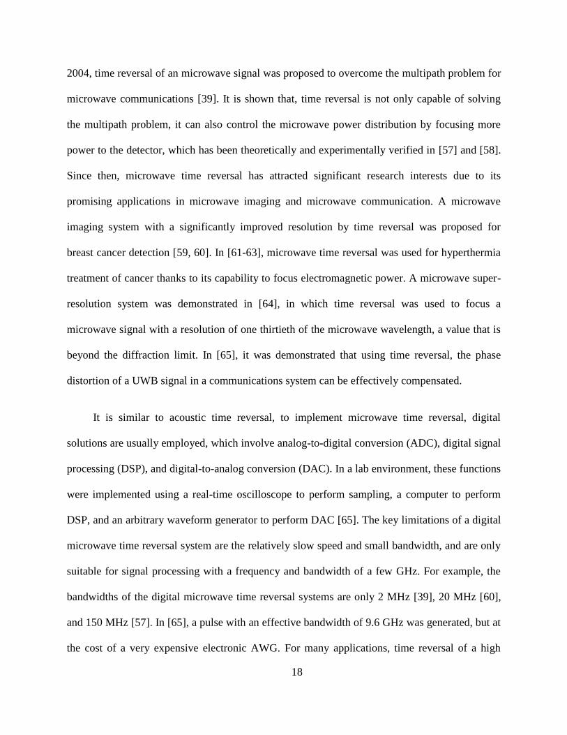
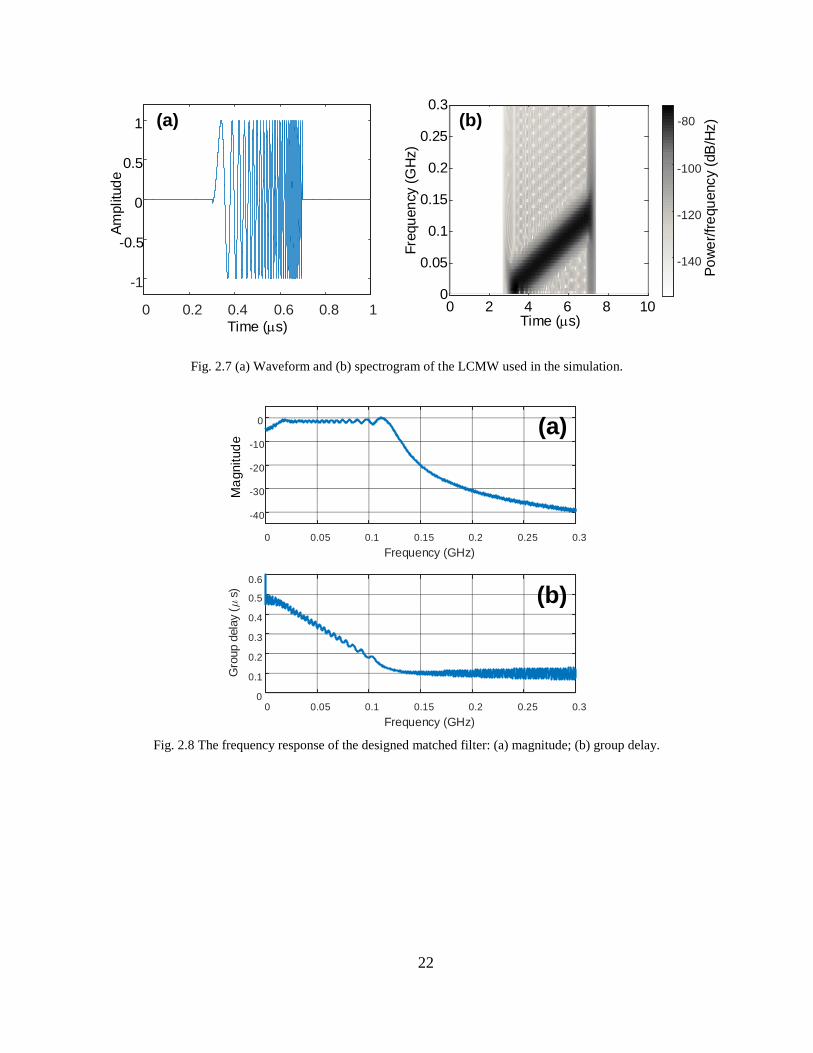
compression of an LCMW is simulated. An LCMW with a temporal duration of 0.4 s and a
bandwidth of 125 MHz is generated. Fig. 2.7 shows the waveform and the corresponding
spectrogram. A linearly increasing instantaneous frequency can be observed, with a chirp rate of
31.3 MHz/s. The TBWP of the signal is calculated to be 50. Then we design a matched filter to
have a group delay dispersion opposite to the chirp rate of the LCMW to perform pulse
compression. The magnitude response and group delay response of the matched filter are shown
in Fig. 2.8, which has a flat-top passband from DC to 125 MHz, and a dispersion of -32 ns/MHz.
The generated LCMW then propagates through the matched filter. A compressed waveform is
derived by multiplying the spectrum of the LCMW and the frequency response of the matched
filter. Fig. 2.9 shows the compressed waveform. A narrow peak with a temporal width of 4.8 ns
is achieved, which indicates a compression ratio of 83.3. It can be seen that, even though the
transmitted signal has a temporal duration of 400 ns, a time resolution of 4.8 ns can be achieved
by using a matched filter.
22
-140
-120
-100
-80
Time (s)
Fre
qu
en
cy (
GH
z)
0 2 4 6 8 100
0.05
0.1
0.15
0.2
0.25
0.3
Po
we
r/fr
equ
ency (
dB
/Hz)
0 0.2 0.4 0.6 0.8 1
-1
-0.5
0
0.5
1
Time (s)
Am
plitu
de
(a) (b)
Fig. 2.7 (a) Waveform and (b) spectrogram of the LCMW used in the simulation.
0 0.05 0.1 0.15 0.2 0.25 0.3
Frequency (GHz)
-40
-30
-20
-10
0
Pow
er
(dB
m)
0 0.05 0.1 0.15 0.2 0.25 0.3
Frequency (GHz)
0
0.1
0.2
0.3
0.4
0.5
Gro
up
dela
y (
s)
0.6
(a)
(b)
Ma
gnitud
e
Fig. 2.8 The frequency response of the designed matched filter: (a) magnitude; (b) group delay.

23
-0.4 -0.3 -0.2 -0.1 0 0.1 0.2 0.3 0.4
Time (s)
-1
0
1
2
Am
plit
ude
Fig. 2.9 The compressed pulse with a pulse width of 4.8 ns.
Then we show the compression of a binary phase-coded waveform using signal cross-
correlation technique, where the transmitted pulse is used as a reference to cross-correlate with
the received signal. A peak will be observed when the received signal matches the reference.
Again, a microwave waveform with 16-bit pseudorandom binary phase code is generated at a bit
rate of 200 Mbit/s and a carrier frequency of 1 GHz, as shown in Fig. 2.10. The compressed
pulse is calculated by auto-correlating the waveform. The correlation result is shown in Fig. 2.11.
A peak with a width of 4.3 ns can be seen, corresponding to a compression ratio of 18.6, which is
approximately equal to the number of phase code bits used in the simulation. Further simulation
shows that the randomly generated phase codes only influences the sidelobe suppression ratio
(relating to the signal-to-noise ratio of the microwave receiver) but not the pulse compression
ratio.

24
Fig. 2.10 The 16-bit pseudorandom binary phase coded signal (blue) and the phase code (red × ).
Compressed width
Outp
ut
Fig. 2.11 The waveform achieved by compressing the phase coded waveform using cross-correlation technique.
It should be noted that pulse compressing based on matched filtering and signal cross-
correlation are two identical processes mathematically. Matched filtering is realized in frequency
domain, while the cross-correlation is performed in time domain.
Photonic techniques have been extensively investigated for the generation of spread-
spectrum microwave waveforms, including LCMWs [70-85] and PCMWs [86-88].On the other

25
hand, very few photonic techniques have been proposed for microwave pulse compression. For
the compression of an LCMW in the electrical domain, a dispersive filter with its spectral
response that is a complex conjugate version of the spectrum of the LCWM can be used as a
matched filter, which can be implemented using a SAW device [89], a C-section delay line [90]
or a synthesized microwave phaser [91]. However, the bandwidth of an electrical matched filter
[89-91] is usually limited to less than a few GHz. A photonic matched filter has the potential to
overcome the bandwidth limitation when used for pulse compression in a radar system. In [92],
an MPF with a quadratic phase response was demonstrated for LCMW compression, in which
the MPF was implemented by passing a single sideband modulated optical signal through an
FBG that has a quadratic phase response. Thanks to optical phase to microwave phase
conversion through single sideband modulation and heterodyne detection, an MPF with a
quadratic phase response was achieved. The bandwidth of the MPF was 3 GHz, which can be
much wider if the FBG is designED to have a wider bandwidth. In [93], a four-tap MPF was
experimentally demonstrated to function as a matched filter for pulse compression of a binary
PCMW with a carrier frequency of 6.75 GHz. The filter can be reconfigured by changing the
wavelength spacing of the optical carriers to compress a microwave waveform with a different
phase coding. Since the tap number is determined by the code length of the PCMW, which can
be long, thus the system is complicated for long length code compression. In [94], an MPF with a
quadratic phase response was demonstrated based on a broadband optical source sliced by a
Mach-Zehnder interferometer (MZI). By passing the sliced optical wave through a nonlinear
dispersive element, a finite impulse response (FIR) filter with nonuniform tap spacing
corresponding to a quadratic phase response was implemented. A bandwidth of 2.5 GHz and a
dispersion of 12 ns/GHz were experimentally achieved. A similar approach was proposed in [95].

26
To eliminate the dispersion induced power penalty, a phase modulator placed in one arm of the
MZI was used instead of an intensity modulator that was placed at the output of the MZI. The
bandwidth of the MPF was 4 GHz.
2.2.3 Temporal convolution
Another approach to realizing pulse compression is by signal correlation or convolution, in
which a received signal is correlated with a reference signal. Signal correlation or convolution
performs pulse compression in time domain and hence offers better configurability for
microwave receivers. Here we use the convolution operation as an example. The temporal
convolution of two signals is different from a filtering operation where a microwave signal is
convolved with the impulse response of a microwave filter due to the multiplication between the
spectrum of the signal and the frequency response of the filter. In many cases, the temporal
convolution can provide better flexibility in signal processing as compared to a filtering
operation since the spectral response of a filter is fixed, but for many signal processing
applications, the spectra of the two microwave signals to be convolved need to be updated in real
time. For example, the temporal convolution was used for the real-time distortion correction in
imaging processing in [96]. Image deblur was achieved by the convolution between the image
data and an impulse response function measured for the specific distortion. In [97], the detection
of the phase information of a periodic signal in noise is realized by convolving the corrupted
signal with its cumulant (accumulation with certain algorithm) version. The convolution in [96]
and [97] are done by digital signal processing techniques. The convolution of two signals based
on an analog system, especially a photonic analog system, has a potential to achieve a high
operation speed for such applications.

27
Temporal convolution is more complex to implement compared to other signal processing
functions that mentioned previously [37, 67, 68, 98-111], as it requires a combination of time
reversal, time delay, signal multiplication and integration. However, thanks to the development
of photonic signal processing in the past few decades, most of the operations have been
demonstrated using photonic techniques.
Photonic microwave time reversal was first demonstrated in [67, 68], which has achieved
an extremely long reversing time window of 6 s using three photon echo effect. However, the
operation bandwidth is only limited to 10 MHz. In [100, 101], we demonstrated that a wideband
microwave waveform can be temporally reversed by a single LCFBG, in which we achieved a
precise time reversal with an operation bandwidth of 4 GHz within a time window of 10 ns. The
microwave time reversals reported in [67, 68, 100, 101] can be good candidates for a temporal
convolution calculation.
On the other hand, photonic integrators for both optical and microwave signals are also
widely reported, which can be realized using an FBG [102], a microring resonator [103, 104], an
active Fabry-Perot cavity [105] or an optical dispersive device [106-109]. The multiplication of
microwave signals can be easily achieved by cascading two electro-optical modulators. The only
challenge in realizing a temporal convolution is to realize a changing time delay difference
between the two signals to be convolved.
2.3 Signal Processing Based on a Dispersive Loop
The maximum dispersion of an LCFBG-based DDL is limited by its physical length when
the operation bandwidth is fixed. However, a DDL with a large dispersion coefficient is required

28
in many signal processing systems. In this section, three signal processing systems implemented
based on a dispersive loop with a large dispersion coefficient is investigated, including a
microwave time-stretched sampling system, a large TBWP waveform generation system and
true-time delay beamforming system.
2.3.1 Time-stretched sampling
For time reversal, pulse compression and temporal convolution introduced above, an
optical DDL may be able to provide a sufficiently large time delay to the order of 10 ns within a
bandwidth of a few hundred GHz. However, there are applications where an even larger
dispersive group delay is required, such as time-stretched sampling.
The ever-increasing bandwidth of modern microwave sensing and communications
systems has imposed new challenges on signal processors to operate at a very high sampling rate.
The use of the conventional sampling techniques may not be able to meet the demand. To realize
broadband sampling, a solution is to use photonic-assisted sub-Nyquist sampling. Numerous
approaches have been proposed, such as optical down-sampling [112, 113], optical
undersampling [114], optical pseudorandom sampling [115], compressive sampling [116], and
optical time stretched sampling [41-49]. Among these techniques, the optical time-stretched
sampling has been considered an effective solution for wideband microwave signal processing.
In an optical time-stretched sampling system, a microwave waveform is modulated on a
pre-dispersed optical pulse, which, after the modulation, travels through another dispersive
element for time stretching. The second dispersive element should have a much greater group
delay dispersion (GDD) coefficient than the first element. A time-stretched microwave

29
waveform will be generated when the pulse is sent to a PD and a slow version of the original
waveform is obtained [70]. This technique was first proposed by Coppinger et al. in [42],
demonstrating a sampling rate that is 1/3.25 of the Nyquist frequency. Since then, new efforts
have been dedicated to further reduce the sampling rate by increasing the stretching factor. In
[43], dispersion-based time stretched sampling with a stretching factor of 5 combined with
compressive sensing was demonstrated to achieve to a sampling rate as low as only 1/40 of the
Nyquist frequency. The sampling rate is then further reduced to 1/80 of the Nyquist frequency by
using a time stretched sampling module with a time stretching factor of 20 [44]. In [45], time-
stretched sampling using a coherent receiver to improve the detection sensitivity by cancelling
the dispersion-induced impairments and optical nonlinearity was demonstrated. A stretching
factor of 24 was achieved by using two dispersive elements with two GDD coefficients of 45 and
1045 ps/nm for the pre-dispersion and time stretching, respectively. In [46], time-stretched
sampling of a continuous-time signal was demonstrated based on virtual time gating, where a
stretching factor of 1.5 was achieved. To overcome the “big data” problem associated with time-
stretched sampling, Asghari et al. demonstrated a sampling solution based on nonlinear time
stretching [47]. An equivalent stretching factor of 200 was achieved. The system has been further
enhanced to achieve real-time bandwidth suppression factor of 500 [48]. In the system, a
programmable optical filter was used to modulate the microwave waveform to the optical pulse,
which may make the system complicated and costly. In [49], an unprecedented time stretching
factor of 250 was realized by using a pre-dispersion element with a GDD coefficient of 41 ps/nm
and a double-pass dispersive element with a GDD coefficient of -10246 ps/nm. To achieve such
a large dispersion, an extremely long DCF is used. To compensate for the loss in the long DCF,
four stimulated Raman amplifiers pumped by four high-power laser diodes were employed.
30
Although the system could realize an effective sampling rate of 10 Tsamples/s, the use of a long
DCF and multiple Raman amplifiers makes the system rather bulky and complicated. For a time
stretching element with a fixed GDD coefficient, to achieve a large stretching factor, the pre-
dispersion element could be selected to have a relatively small GDD coefficient. The
consequence of using a pre-dispersion element with small dispersion is that the input optical
pulse cannot be sufficiently pre-stretched to have a large time duration, to allow a microwave
waveform with a long duration to be modulated on the pre-stretched input pulse. Therefore, the
fundamental solution to have a large stretching factor for a long-duration microwave waveform
is to use a time stretching element with a large GDD coefficient.
In fiber optics, a dispersive element can be an SMF, a DCF, or an LCFBG. Since an SMF
has a relatively small dispersion coefficient, it is rarely used in a time stretched sampling system,
especially as the time-stretching dispersive element. A DCF, on the other hand, can have a
dispersion coefficient that is several times greater than that of an SMF. However, to achieve
large time stretching, a DCF with a length of several tens [45] or even hundreds [49] of km is
required. Thus, the system is still bulky and lossy. An LCFBG has been proved to be a highly
effective dispersive element with low insertion loss and small nonlinear effects [27, 117]. The
GDD of an LCFBG is proportional to its grating length and inversely proportional to its
bandwidth. For time stretching applications, the bandwidth of an LCFBG is usually controlled to
be equal to the bandwidth of the optical pulse. Hence, to have a large GDD coefficient, an
LCFBG with a long length is needed. For example, a 10-cm long LCFBG with 1-nm bandwidth
has a GDD coefficient of 1000 ps/nm. To further increase the GDD coefficient, the length of the
LCFBG should be further increased. Although an LCFBG with a length greater than 1 m is
commercially available, the size is large and the fabrication is complicated and costly.

31
The use of a microwave waveguide with a large GDD coefficient has been explored in the
past few years for spectrum analysis [118, 119]. Recently, it was demonstrated [120] that by
forming a dispersive loop that incorporates a microwave dispersive element and a microwave
amplifier, an equivalent microwave dispersive element with a GDD coefficient that is several
times greater than that of the original dispersive element can be achieved by recirculating the
microwave waveform in the loop. Compared with a simple cascade of multiple dispersive
elements to achieve an equivalent dispersive element with a large GDD coefficient, the
recirculating dispersive loop has the advantages such as a smaller device footprint, lower
insertion loss (less than 3 dB loss per round trip compared to tens of dB of a long optical fiber)
and better signal-to-noise ratio (SNR) [120]. The major limitations of an electrical dispersive
loop are the small bandwidth, usually below 1 GHz, and high loss. In addition, the maximum
time delay is limited, although the constant time delay provided by a coaxial cable is already
much larger compared to that of a waveguide. To implement a dispersive loop with a large GDD
coefficient over a large bandwidth, a solution is to use photonic components. In addition to a
broad bandwidth, an optical dispersive loop can generate a much longer time delay since a long
loop length of several kilometers is possible due to the low loss of an optical fiber. A time-
stretched sampling system using an optical dispersive loop can significantly increase the
stretching factor over a broad bandwidth.
2.3.2 Large time-bandwidth product signal generation
An optical DDL with an extremely large dispersion coefficient may also be used in a
photonic microwave AWG for the generation of a waveform with a large TBWP. Microwave
waveforms with a large TBWP have been widely employed in microwave sensors [121, 122],

32
spread-spectrum communications [123], microwave computed tomography [124], and modern
instrumentation. For example, in an active microwave sensor, an LCMW with a large TBWP can
be used to improve the range resolution. An LCMW are usually generated electronically, and the
temporal duration can be long. However, due to the limited speed of the currently available
electronic circuits, the bandwidth and the central frequency of an LCMW generated
electronically are usually limited to a few GHz [125-127]. An LCMW with a central frequency
and a bandwidth up to tens or even hundreds of GHz may be required in a modern microwave
sensor to improve the sensing resolution.
Numerous photonic approaches have been proposed and demonstrated for the generation of
an LCMW with a large TBWP [70]. These approaches can be generally classified into three
categories: space-to-time pulse shaping [71-73], SS-WTT mapping [74-76, 80-84], and temporal
pulse shaping [77]. An LCMW can also be generated using an MPF [78] with a quadratic phase
response, using an optoelectronic oscillator (OEO) [85], or optical heterodyning [79]. A space-
to-time pulse shaping system is usually implemented using a spatial light modulator (SLM). The
SLM has the flexibility in updating in real time the pattern on the SLM, which enables the
generation of an arbitrary microwave waveform. The major limitations of using an SLM are the
relatively high loss and large size [71], [72]. Although the SLM in a space-to-time pulse shaping
system can be replaced by an arrayed waveguide grating, the maximum temporal duration of the
generated waveform is still limited, in a range of tens of picoseconds, due to the relatively small
channel number of an arrayed waveguide grating, developed usually for wavelength-division
multiplexing communications applications [73]. Microwave waveform generation based on
temporal pulse shaping, an MPF, or an OEO, also has the limitation of small temporal duration.

33
The phase stability of the waveforms generated by optical heterodyne technique is usually poor
[79].
On the other hand, microwave waveform generation based on SS-WTT mapping has the
advantages of simplicity, flexibility and relatively low cost. In an SS-WTT mapping system, an
ultra-short pulse with a wide spectrum is spectrally shaped by an optical spectral shaper. The
shaped spectrum is then mapped to the time domain by a dispersive element to produce a
microwave waveform with a temporal shape that is a scaled version of the spectrum of the
spectrally shaped pulse. Hence, an LCMW can be generated by designing an optical spectral
shaper with a linearly increasing or decreasing free spectral range (FSR), and using a dispersive
element with linear dispersion to perform linear WTT mapping. In [74], a fiber-optic spectral
shaper with a Michelson interferometer structure using two LCFBGs as two reflectors was
proposed and demonstrated for LCMW generation. Due to the wavelength-dependent length
difference between the two arms of the Michelson interferometer, a linearly decreasing FSR is
achieved which is needed for LCMW generation. In addition to the operation as two reflectors,
the LCFBGs also function as a dispersive element to perform linear WTT mapping. An LCMW
with a TBWP of around 15 was generated. In [80], an optical spectral shaper was realized by
employing two LCFBGs with different chirp rates that are fabricated and superimposed in a fiber.
The two LCFBGs form a Fabry-Perot (FP) cavity to have a spectral response with a linearly
decreasing or increasing FSR due to the wavelength-dependent cavity length. The use of the
spectral shaper to generate an LCMW was demonstrated. An LCMW with a TBWP of 37.5 was
achieved. In [81], a spectral shaper implemented using a Sagnac loop mirror with an LCFBG in
the loop was reported. Again, a spectral response with a linearly decreasing or increasing FSR
was resulted due to the wavelength-dependent loop length. An LCMW with a TBWP of 44.8 was
34
experimentally generated. In [82] , a tilted fiber Bragg grating (TFBG) fabricated in an
erbium/ytterbium co-doped fiber was used as a spectral shaper. Since the spectral response of the
spectral shaper can be tuned by optically pumping the TFBG, the generation of an LCMW with a
tunable chirp rate from 1.8 to 7 GHz/ns was demonstrated. In [83], a configurable microwave
waveform generator with a bandwidth up to 60 GHz based on a silicon photonic chip was
demonstrated. However, the temporal duration of the waveforms generated in [82] and [83] are
limited to 1 ns, with TBWPs of less than 60. In [84], a microwave waveform generator based on
SS-WTT mapping was proposed, in which an electrically stabilized MZI was used as the spectral
shaper and a DCF was used to perform WTT. A microwave waveform with a temporal duration
of 16 ns and a TBWP of 589 was achieved. Using a similar scheme, an LCMW with a TBWP of
600 was generated thanks to the use of a near-ballistic uni-traveling-carrier photodiode with a
large bandwidth of over 175 GHz [75]. However, the temporal duration of the microwave
waveform is only 15 ns, which is still small for many applications. In [76], a microwave
waveform with an arbitrarily long temporal duration was generated by synthesizing a series of
LCMWs with different phases. An individual segment of the waveform is an LCMW generated
by SS-WTT, in which a programmable optical filter and two modulators are needed which would
increase the system complexity. In addition, the temporal duration of an individual segment of
the LCMW is only 5 ns. Although the techniques in [74-76, 80-84] can be used to generate an
LCMW with a wide bandwidth and a high carrier frequency of over tens of GHz, the temporal
duration is usually small which is fundamentally limited by the achievable maximum time delay
of the dispersive device used for WTT mapping. For example, the maximum time delay of an
LCFBG is only a few nanoseconds, limited by its physical length [27]. Although a DCF with a
length of tens of kilometers can achieve a larger dispersion, the high insertion loss needs to be
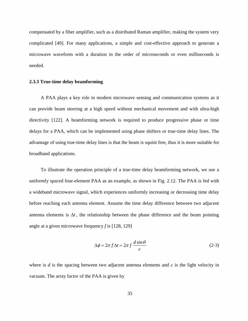
35
compensated by a fiber amplifier, such as a distributed Raman amplifier, making the system very
complicated [49]. For many applications, a simple and cost-effective approach to generate a
microwave waveform with a duration in the order of microseconds or even milliseconds is
needed.
2.3.3 True-time delay beamforming
A PAA plays a key role in modern microwave sensing and communication systems as it
can provide beam steering at a high speed without mechanical movement and with ultra-high
directivity [122]. A beamforming network is required to produce progressive phase or time
delays for a PAA, which can be implemented using phase shifters or true-time delay lines. The
advantage of using true-time delay lines is that the beam is squint free, thus it is more suitable for
broadband applications.
To illustrate the operation principle of a true-time delay beamforming network, we use a
uniformly spaced four-element PAA as an example, as shown in Fig. 2.12. The PAA is fed with
a wideband microwave signal, which experiences uniformly increasing or decreasing time delay
before reaching each antenna element. Assume the time delay difference between two adjacent
antenna elements is t , the relationship between the phase difference and the beam pointing
angle at a given microwave frequency f is [128, 129]
sin2 2
df t f
c
(2-3)
where is d is the spacing between two adjacent antenna elements and c is the light velocity in
vacuum. The array factor of the PAA is given by
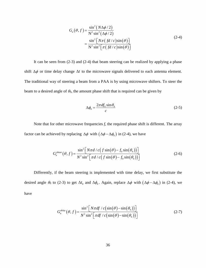
36
2
2 2
2
2 2
sin / 2,
N sin / 2
sin / sin
N sin / sin
a
NG f
N fd c
fd c
(2-4)
It can be seen from (2-3) and (2-4) that beam steering can be realized by applying a phase
shift or time delay change t to the microwave signals delivered to each antenna element.
The traditional way of steering a beam from a PAA is by using microwave shifters. To steer the
beam to a desired angle of 0, the amount phase shift that is required can be given by
0 00
2 sindf
c
(2-5)
Note that for other microwave frequencies f, the required phase shift is different. The array
factor can be achieved by replacing with 0 in (2-4), we have
2
0 0
2 2
0 0
sin / sin sin,
sin / sin sin
phase
a
N d c f fG f
N d c f f
(2-6)
Differently, if the beam steering is implemented with time delay, we first substitute the
desired angle 0 to (2-3) to get 0t and 0 . Again, replace with 0 in (2-4), we
have
2
0
2 2
0
sin / sin sin,
sin / sin sin
delay
a
N df cG f
N df c
(2-7)
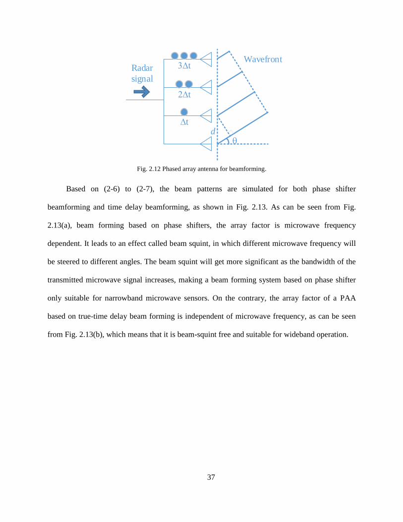
37
d
WavefrontRadar
signal
t
2t
3t
Fig. 2.12 Phased array antenna for beamforming.
Based on (2-6) to (2-7), the beam patterns are simulated for both phase shifter
beamforming and time delay beamforming, as shown in Fig. 2.13. As can be seen from Fig.
2.13(a), beam forming based on phase shifters, the array factor is microwave frequency
dependent. It leads to an effect called beam squint, in which different microwave frequency will
be steered to different angles. The beam squint will get more significant as the bandwidth of the
transmitted microwave signal increases, making a beam forming system based on phase shifter
only suitable for narrowband microwave sensors. On the contrary, the array factor of a PAA
based on true-time delay beam forming is independent of microwave frequency, as can be seen
from Fig. 2.13(b), which means that it is beam-squint free and suitable for wideband operation.
38
(a)
(b)
Fig. 2.13 (a) Beam pattern with phase shifter steering; (b) beam pattern with time delay beam forming. In the
simulation: N=40; d=1.5 cm; f0=10 GHz.
A true time delay beamforming network can be realized using electronic delay lines, but
with a small bandwidth, a large size and a high loss [130, 131]. In the past few years, numerous
photonic true-time delay beamforming networks have been demonstrated. In [132], a free space
photonic true-time delay network was demonstrated. The time delay of a microwave signal
modulated on an optical carrier is changed by changing the polarization state of the optical
carrier so that it can travel through different optical paths. As a free-space optical system
generally requires a large number of mirrors and lenses, it is usually very heavy and bulky. Fiber
optics and photonic integrated circuits can be used to mitigate these limitations thanks to their
small size and low loss. In [133], an FBG array was used to realize true-time delays. The
tunability of the time delays was achieved by changing the optical carrier wavelengths. A

39
maximum true time delay of 233 ps was experimentally demonstrated. Since an FBG array
contains a large number of FBGs, to reduce the complexity, in [134] a true-time delay network
implemented using a single LCFBG was proposed. Since optical carriers with different
wavelengths are reflected at different locations in an LCFBG, different time delays can be
achieved for a microwave signal modulated on different optical carriers. In addition, tunable time
delays can be achieved by changing the chirp rate of the LCFBG. A time delay tuning range of
100 ps, with a tuning step of 1 ps was demonstrated. In [135], a DCF was used instead of an
LCFBG. Tunable true-time delays were achieved by changing the optical carrier wavelengths.
Similarly, in [136] an SMF is used as a dispersion element to realize tunable time delay by
changing the wavelengths of an optical frequency comb, which is used as the optical carriers for
multiple microwave signals. A fiber-optics based beamforming network features a smaller size,
but a TLS is usually required in [133, 135, 136] to achieve a large tunable time delay, making the
system costly. In addition, the wavelength stability due to tuning may deteriorate, which will
affect the time delay accuracy. In [137], instead of using TLSs, a tunable dispersive medium
based on the similar effect in [134] was used to implement tunable true-time delay. A true-time
delay with a tuning range of 200 ps was demonstrated, which is again very limited. In [138], a
multicore fiber was employed to achieve tunable true-time delay. By designing the refractive
index profile of the fiber, optical signals travels in different cores will experience different time
delays. However, the time delay cannot be conveniently tuned. Photonic true-time delay can also
be realized based on SBS [139]. In the gain SBS spectrum, the time delay is wavelength
dependent. By changing the optical carrier wavelength which is placed in the SBS spectrum
profile, the time delay is tuned. However, the spectral width of an SBS gain profile is very small,
which limits the bandwidth of the microwave signal modulated on the optical carrier. Other

40
techniques to achieve true-time delays include the use of stack integrated micro-optical
components [140]. Since movable prism groups are used, the reliability is poor. Recently, an on-
chip microwave photonic beamformer based on Si3N4/SiO2 waveguide technology was
demonstrated [141, 142]. The stability is better than using fiber delay lines. Due to the small size
of the chip, the achievable time delay is small, limited to a few hundreds of ps. In [143], a
photonic microwave filter was designed to have a frequency response that is similar to a
microwave delay line with a tunable time delay. An integrated-optics based beamforming
network has an ultra-smaller size, but only small time delays are achievable due to the small size
of the chip [140-143].
2.4 Summary
In this Chapter, signal processing functions based on FBG-based dispersive delay lines
have been discussed. First, an introduction to an FBG was given. An LCFBG and a dispersive
loop used to achieve a tunable time delay were also discussed. Then, signal processing functions
that can be realized by an LCFBG-based DDL or a dispersive loop were introduced, including
time reversal, pulse compression and temporal convolution that can be implemented with a
single LCFBG as a DDL, and time-stretched sampling, large TBWP waveform generation and
true-time delay beamforming that requires the use of a dispersive loop for a large dispersion
coefficient.

41
CHAPTER 3 MICROWAVE TIME REVERSAL
Time reversal is one of the basic signal processing functions that can find numerous
applications, such as increasing the resolution of an acoustic or microwave imaging system,
solving the multipath problem in a microwave communication system, cancer detection and
treatment. Current time reversal modules are usually implemented with digital electronics, which
is limited to a bandwidth of a few GHz and cannot meet the requirement of broadband
microwave imaging and communication systems
In this chapter, we propose and experimentally demonstrate a novel technique to achieve
broadband and precise microwave time reversal using a single LCFBG as an optical DDL. In the
proposed system, the time reversal is realized by the LCFBG that is operating in conjunction
with a polarization beam splitter (PBS) to enable a triple use of the LCFBG with the microwave
waveform entering the LCFBG from either the long or the short wavelength end. Since the
LCFBG has a wide bandwidth and is used three times with exactly complementary and identical
dispersion, broadband and precise microwave time reversal is ensured. A theoretical analysis is
performed which is validated by simulations and an experiment. The time reversal of three
different microwave waveforms with a bandwidth over 4 GHz and a time duration of about 10 ns
is demonstrated.

42
3.1 Operation Principle
In this section, the operation principle of the proposed time reversal system is investigated.
A mathematical model is developed to quantitatively describe the waveform distortion and
bandwidth limit of the system.
3.1.1 System architecture
Fig. 3.1 shows the proposed microwave photonic system for broadband and precise
microwave time reversal. A transform-limited optical pulse generated by a mode-lock laser
(MLL) is filtered by a bandpass optical filter (OF) with a bandwidth of 4 nm, and sent to the
LCFBG from its long wavelength end via a 3-port optical circulator (OC1). The optical pulse is
then temporally stretched by the LCFBG. The LCFBG has a reflectivity of over 95% and a
bandwidth of 4 nm which is equal to the spectral width of the optical pulse from the OF. Hence,
the optical pulse from the OF is almost completely reflected by the LCFBG and the transmission
is small and negligible. At the third port of OC1, a Mach-Zehnder modulator (MZM) is
connected, to which a microwave waveform to be temporally reversed is applied. A polarization
controller (PC1) is incorporated between OC1 and the MZM to align the polarization state of the
optical pulse to the principal axis of the MZM, to minimize the polarization-dependent loss. At
the output of the MZM, the optical pulse is directed into a 4-port optical circulator (OC2). A PBS
is used to connect the short wavelength end of the LCFBG to the second and third ports of OC2.
Two other PCs (PC2 and PC3) are employed between the PBS and OC2 to control the
polarization directions of the light waves to the PBS, so that the light waves can be efficiently
coupled to the LCFBG by the PBS. The optical pulse injected to the 1st port of OC2 is directed
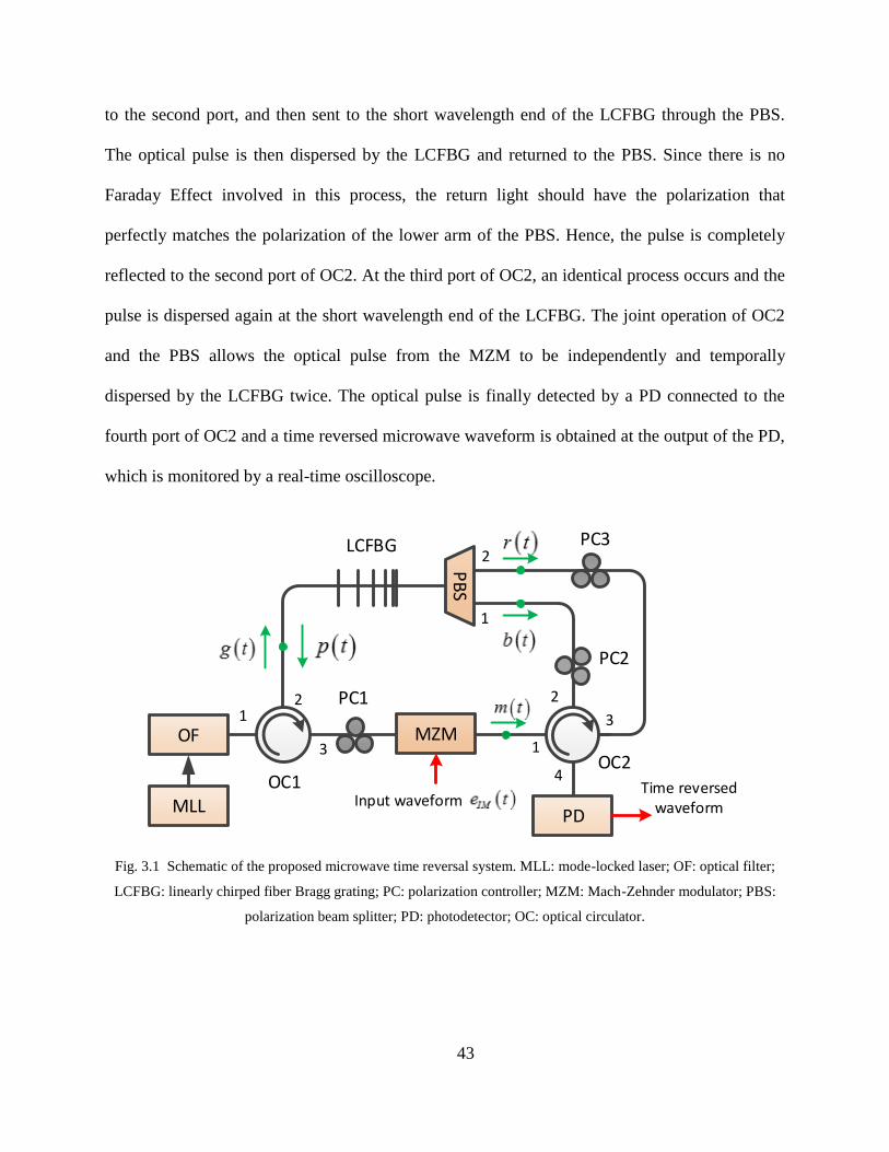
43
to the second port, and then sent to the short wavelength end of the LCFBG through the PBS.
The optical pulse is then dispersed by the LCFBG and returned to the PBS. Since there is no
Faraday Effect involved in this process, the return light should have the polarization that
perfectly matches the polarization of the lower arm of the PBS. Hence, the pulse is completely
reflected to the second port of OC2. At the third port of OC2, an identical process occurs and the
pulse is dispersed again at the short wavelength end of the LCFBG. The joint operation of OC2
and the PBS allows the optical pulse from the MZM to be independently and temporally
dispersed by the LCFBG twice. The optical pulse is finally detected by a PD connected to the
fourth port of OC2 and a time reversed microwave waveform is obtained at the output of the PD,
which is monitored by a real-time oscilloscope.
OF MZM
PB
S
PD
OC1OC2
LCFBG
PC2
PC3
PC11
2
3
4
1
2
3
Time reversedwaveformMLL Input waveform
1
2
Fig. 3.1 Schematic of the proposed microwave time reversal system. MLL: mode-locked laser; OF: optical filter;
LCFBG: linearly chirped fiber Bragg grating; PC: polarization controller; MZM: Mach-Zehnder modulator; PBS:
polarization beam splitter; PD: photodetector; OC: optical circulator.
44
3.1.2 Time reversal modeling
Mathematically, the LCFBG can be modeled as a linear and time-invariant (LTI) system
with a quadratic phase response and unity amplitude response. Assuming that the electrical field
of the optical pulse from the OF is g(t), after being dispersed by the LCFBG (entering from the
long wavelength end), the electrical field of the optical pulse at the third port of OC1 is given by
[70]
2
exp2
tp t g t j
(3-1)
where is the dispersion coefficient of the LCFBG looking into it from the long wavelength
end, and * denote the convolution operation.
Note that the dispersion coefficient looking into the LCFBG from the short wavelength end
is . Fig. 3.2 shows the reflection spectrum of an LCFBG fabricated based on the holographic
method in a SMF with a length of 1 meter. The spectrum is measured by an optical vector
analyzer (OVA, Luna Technologies). As can be seen the LCFBG has a bandwidth of 4 nm and a
central wavelength of 1551.4 nm, which is approximately equal to the central wavelength of the
pulse spectrum from the OF. The group delay responses of the LCFBG measured from its short
and long wavelength ends are also shown in Fig. 3.2. As can be seen that the group delay
responses are complementary and the dispersion coefficients are +2500 ps/nm and -2500 ps/nm,
corresponding to the green and red lines, respectively. Since the LCFBG has a long length,
which is more than the measurable length of the OVA, in the mesurement the LCFBG is
considered as four cascaded sub-sections, and each sub-section is measured independently. The

45
spectrum of the entire LCFBG is then achieved by synthesizing the four measurements
corresponding to the spectra of the four sub-sections.
1548 1549 1550 1551 1552 1553 1554 1555Wavelength (nm)
Reflectivity (
%)
0
20
40
60
80
100
Gro
up D
ela
y (n
s)
0
2
4
6
8
10
Fig. 3.2 The reflection spectrum and group delay responses of the LCFBG.
MLL MZM
LCFB
G1
PC12
3 12
3
Inputwaveform
Time reversedwaveform
PD1
2
3
LCFB
G2
LCFB
G3TPS system
Fig. 3.3 The implementation of the proposed microwave time reversal system using three LCFBGs.
The microwave time reversal system can be modeled as a temporal pulse shaping (TPS)
system [70] with a pair of complementary dispersive elements of and , followed by a
residual dispersion of , as shown in Fig. 3.3. As can be seen the implementation of the system
46
based on our proposed configuration in Fig. 3.1 to use only a single LCFBG significantly
reduces the complexity and improve the performance (with no dispersion mismatch).
The electrical field at the output of the MZM is given by
IMm t p t e t (3-2)
where IMe t is the microwave signal applied to the MZM.
After being dispersed by the LCFBG entering from the short wavelength end of the
LCFBG for the first time, the electrical field becomes
2
exp2
tb t m t j
(3-3)
If the duration of the MLL pulse 0 and the dispersion of the LCFBG (in ps2) satisfy
the far field condition 2
0 / 1 , the Fraunhofer approximation can be adopted. Substituting
(3-1) and (3-2) into (3-3), we have [144, 145]
/IM t
b t g t E
(3-4)
where IME is the Fourier transform of IMe t .
The electrical field at the output of the entire time reversal system r(t) is obtained by
propagating the optical signal b t from the temporal pulse shaping system through a third
dispersive element with a value of residual dispersion of via the fourth port of OC2 [70],

47
2
exp2 t
jtr t B
(3-5)
where B() is the Fourier transform of b(t).
Substitute (3-4) into (3-5), we have
2
2
2
exp2
exp2 2
exp2 2
IMt
IM
t
IM
jt tr t F g t E
jtG e
jt tG e t
(3-6)
where G() is the Fourier transform of g(t).
The optical pulse at the fourth port of OC2 is detected by the PD. The generated
photocurrent is given by
2 2 2
IM
tI t r t G e t
(3-7)
where is the responsivity of the PD.
3.1.3 Waveform distortion
As can be seen from (7) the microwave waveform at the output of the system is a time-
reversed version of the input signal except for a multiplying term 2 /G t . Ideally, the optical

48
pulse from the MLL is ultra-short, and its temporally dispersed version is ultra-wide and flat,
which will have small impact on the generated waveform. To study the impact of 2 /G t on
the generated time-reversed waveform, a simulation is performed, in which the dispersive
element is a real LCFBG which has a spectral response given in Fig. 3.2. An up-chirped
microwave waveform shown in Fig. 3.4 (solid line) is used as the input signal IMe t . The
microwave waveform at the output of the PD is frequency down-chirped, which is a time-
reversed version of the input waveform, except for a slowly-varying envelope due to /G t .
In the simulation, /G t is the optical spectrum of an optical pulse from the MLL after
being filtered by the bandpass OF and reflected three times by the LCFBG. From Fig. 3.4 it can
be seen that the output waveform has exactly the same temporal duration and shape as compared
with the input microwave waveform. Note that to ease the comparison, the generated time-
reversed waveform is flipped horizontally and shown on the same figure. A correlation
coefficient [146] of 0.998 is achieved between the original and the time reversed signal. The very
small envelope distortion is induced by 2 /G t , which can be further suppressed by using an
MLL with a flatter optical spectrum and an LCFBG with more uniform reflectivity.

49
0 2 4 6 8 10 12 14
0
0.2
0.4
0.6
0.8
1
Time for original signal (ns)
No
rmaliz
ed M
ag
nitud
e
02468101214Time for reversed signal (ns)
Fig. 3.4 The simulated time reversed waveform considering the impact from 2 /G t . Dotted: input up-
chirped waveform; dash: time-reversed output waveform with a frequency down-chip; solid: the profile of
2 /G t , determined by the spectrum of the optical pulse from the MLL and the dispersion of the LCFBG.
3.1.4 Electrical and optical bandwidth limit
The limited bandwidth is another factor that may influence the performance of the time
reversal operation. In the proposed system, the bandwidth of the LCFBG is very wide, and the
system bandwidth is mainly limited by the electronic components used, including the electronic
amplifiers, MZM and the PD. Fig. 3.5 shows the distortion caused by the limited electronic
bandwidth. Similar to Fig. 3.4, a frequency up-chirped waveform is used as the input waveform.
At the output, a time-reversed waveform with a reduced amplitude is observed, especially for
high frequency components, when a low-pass filter (3-dB cut-off frequency at 4 GHz) is
employed to emulate the bandwidth limitation of the electronic components. The correlation
coefficient between the original and the time-reversed waveform is 0.981. As the central
frequency of the input signal increases, the correlation coefficient drops drastically, indicating a
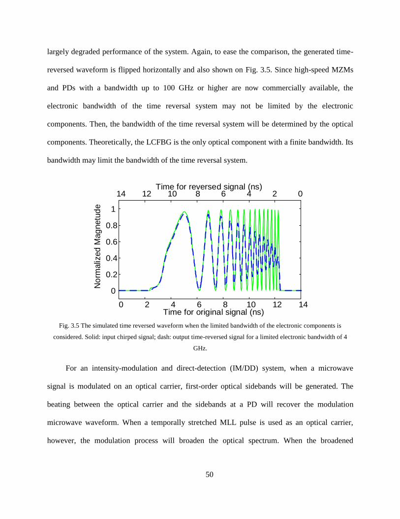
50
largely degraded performance of the system. Again, to ease the comparison, the generated time-
reversed waveform is flipped horizontally and also shown on Fig. 3.5. Since high-speed MZMs
and PDs with a bandwidth up to 100 GHz or higher are now commercially available, the
electronic bandwidth of the time reversal system may not be limited by the electronic
components. Then, the bandwidth of the time reversal system will be determined by the optical
components. Theoretically, the LCFBG is the only optical component with a finite bandwidth. Its
bandwidth may limit the bandwidth of the time reversal system.
0 2 4 6 8 10 12 14
0
0.2
0.4
0.6
0.8
1
No
rmaliz
ed M
ag
netu
de
Time for reversed signal (ns)02468101214
Time for original signal (ns)
Fig. 3.5 The simulated time reversed waveform when the limited bandwidth of the electronic components is
considered. Solid: input chirped signal; dash: output time-reversed signal for a limited electronic bandwidth of 4
GHz.
For an intensity-modulation and direct-detection (IM/DD) system, when a microwave
signal is modulated on an optical carrier, first-order optical sidebands will be generated. The
beating between the optical carrier and the sidebands at a PD will recover the modulation
microwave waveform. When a temporally stretched MLL pulse is used as an optical carrier,
however, the modulation process will broaden the optical spectrum. When the broadened
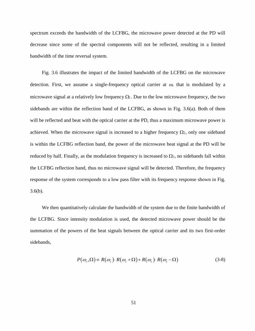
51
spectrum exceeds the bandwidth of the LCFBG, the microwave power detected at the PD will
decrease since some of the spectral components will not be reflected, resulting in a limited
bandwidth of the time reversal system.
Fig. 3.6 illustrates the impact of the limited bandwidth of the LCFBG on the microwave
detection. First, we assume a single-frequency optical carrier at c that is modulated by a
microwave signal at a relatively low frequency . Due to the low microwave frequency, the two
sidebands are within the reflection band of the LCFBG, as shown in Fig. 3.6(a). Both of them
will be reflected and beat with the optical carrier at the PD, thus a maximum microwave power is
achieved. When the microwave signal is increased to a higher frequency 2, only one sideband
is within the LCFBG reflection band, the power of the microwave beat signal at the PD will be
reduced by half. Finally, as the modulation frequency is increased to 3, no sidebands fall within
the LCFBG reflection band, thus no microwave signal will be detected. Therefore, the frequency
response of the system corresponds to a low pass filter with its frequency response shown in Fig.
3.6(b).
We then quantitatively calculate the bandwidth of the system due to the finite bandwidth of
the LCFBG. Since intensity modulation is used, the detected microwave power should be the
summation of the powers of the beat signals between the optical carrier and its two first-order
sidebands,
,c c c c cP R R R R (3-8)

52
where R is the reflectivity of the LCFBG and ,cP represents the optical power
generated by an optical carrier with an angular frequency of c and a unit spectral width. Since
all the spectral components of the optical pulse from the MLL over a frequency range of
contribute to the optical carrier, the total microwave power detected at the PD is
,c cP P d
(3-9)
Based on (3-9) and using the measured LCFBG reflection spectrum shown in Fig. 3.2, the
microwave spectral response of the time reversal system is calculated. As shown in Fig. 3.7, the
system is a low-pass filter with the 3-dB cut-off frequency at 273 GHz, which is approximately
equal to half of the optical bandwidth of the LCFBG.
LC
FB
G S
pectr
um
Fre
qu
en
cy R
esp
onse Optical
frequency
Electrical
frequency
(a)
(b)
Optical
carrier
+1st order
sidebands
0 1 2 3
c
11
2
2
33
Fig. 3.6 The mechanism for the bandwidth limit of the optical part. (a) Optical carrier c and sidebands reflected by
the LCFBG. As modulation frequency increases from 1 to 3, the sidebands may locate outside the reflection band
of LCFBG; (b) the corresponding frequency response of the LCFBG.

53
-16
-12
-8
-4
0
Frequency (GHz)
Tra
nsm
ittivity (
dB
)
100
101
102
103
Fig. 3.7 Microwave spectral response of the time reversal system due to the finite bandwidth of the LCFBG.
3.2 Experimental Implementation
An experiment based on the setup shown in Fig. 3.1 is performed. An optical pulse from
the wavelength tunable MLL (PriTel FFL-1550-20) with a 3-dB bandwidth of 8 nm and a pulse
width less than 600 fs is used as the light source. The repetition rate of the pulse train from the
MLL is 20 MHz. An OF with a bandwidth of 4 nm centered at the spectrum of the MLL is
employed to achieve a flat spectrum and, at the same time, to ensure that the pulse can be
completely reflected by the LCFBG. The LCFBG was fabricated using the holographic method.
A microwave AWG (Tektronix AWG7102) with a sampling rate of 10 Gb/s is used to generate a
microwave waveform that is applied to the MZM (JDSU OC-192, bandwidth of 10 GHz) after
amplified by an electrical amplifier (MTC5515, bandwidth of 10 GHz). The microwave
waveform and the optical pulse from the MLL are synchronized by applying a trigger signal
from the MLL to the arbitrary waveform generator. The optical pulse at the fourth port of OC2 is
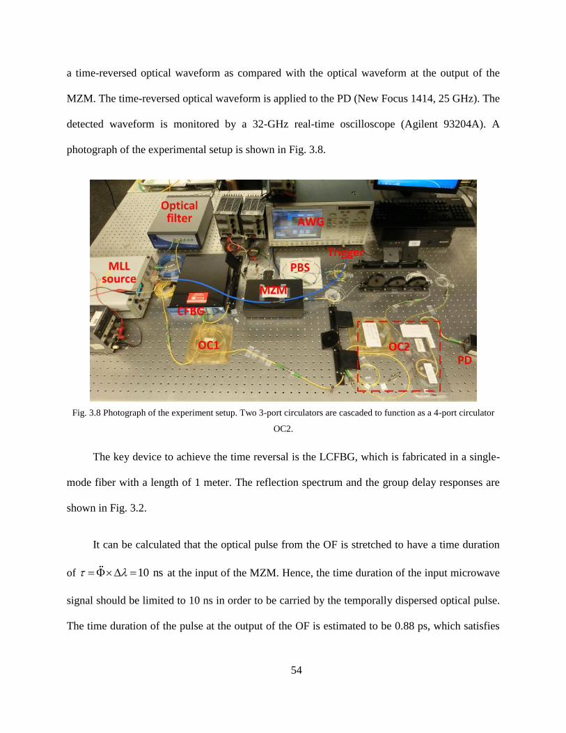
54
a time-reversed optical waveform as compared with the optical waveform at the output of the
MZM. The time-reversed optical waveform is applied to the PD (New Focus 1414, 25 GHz). The
detected waveform is monitored by a 32-GHz real-time oscilloscope (Agilent 93204A). A
photograph of the experimental setup is shown in Fig. 3.8.
Fig. 3.8 Photograph of the experiment setup. Two 3-port circulators are cascaded to function as a 4-port circulator
OC2.
The key device to achieve the time reversal is the LCFBG, which is fabricated in a single-
mode fiber with a length of 1 meter. The reflection spectrum and the group delay responses are
shown in Fig. 3.2.
It can be calculated that the optical pulse from the OF is stretched to have a time duration
of 10 ns at the input of the MZM. Hence, the time duration of the input microwave
signal should be limited to 10 ns in order to be carried by the temporally dispersed optical pulse.
The time duration of the pulse at the output of the OF is estimated to be 0.88 ps, which satisfies

55
the far-field condition for a TPS system [70]. Note that the far-field condition does not need to be
considered when the pulse passing through the LCFBG for the second and third times [41].
3.3 Performance Evaluation
Three different waveforms are generated by the arbitrary waveform generator to test the
operation of the proposed microwave time reversal system. The three waveforms are a sawtooth
wave, a chirped wave, and an arbitrary waveform. To compare an original waveform and a time-
reversed waveform simultaneously, a 3-dB coupler was used after the MZM to direct part of the
modulated optical pulse to a PD and sampled by another channel of the real-time oscilloscope.
Fig. 3.9 shows the microwave waveforms from the two separate channels of the real-time
oscilloscope, which correspond to the waveforms before and after the time reversal. Specifically,
in Fig. 3.9(a), a 3-cycle up-ramp sawtooth is time reversed to become a down-ramp sawtooth. A
small amplitude change in the 3-cycles can be observed, which is caused by the non-ideally flat
spectrum shape of the MLL pulse, as confirmed by the simulation. The amplitude change can be
reduced by improving the flatness of the optical pulse. In Fig. 3.9(b), a frequency up-chirped
microwave waveform with a time duration of 10 ns and a frequency range from DC to 4 GHz is
time reversed to become a frequency down-chirped waveform. Note that the input microwave
waveform is not an ideal frequency-chirped pulse due to the limited sampling rate (10 Gb/s) of
the arbitrary waveform generator, and the limited bandwidth of the electrical amplifier (EA) and
the MZM. In Fig. 3.9(c), an arbitrary waveform is generated by the arbitrary waveform generator
which is also time reversed. It can be seen from Fig. 3.9(a)-(c) that the time-reversed waveforms
have exactly the same time duration and the same shape with the original waveforms, except for

56
very small amplitude distortions caused by the limited bandwidth of the electronic components
and the non-flat spectral shape of the optical pulse. By correlating the original waveforms with a
flipped version of the time reversed waveforms, we have three correlation coefficients of 0.930,
0.939 and 0.951, which are slightly smaller than the theoretical values of 1 due to the existence
of system noise. Nevertheless, precise and single shot time reversal of a microwave waveform
with a bandwidth up to 4 GHz and a time duration of 10 ns has been achieved.
40 45 50 55 60 65 70 75
Time (ns)
Volta
ge (
mV
)
0
10
20
30
40
50
60 (a)Original
Reversed
40 45 50 55 60 65 70 75
0
20
40
60
80
Time (ns)
Volta
ge (
mV
)
(b)
Original
Reversed

57
40 45 50 55 60 65 70 75Time (ns)
Volta
ge (
mV
)
0
10
20
30
40
50
60 (c)
Original
Reversed
Fig. 3.9 Comparison between the original and the time reversed waveforms. (a) sawtooth wave; (b) chirped wave;
(c) arbitrary waveform. The corresponding correlation coefficients are calculated to be 0.930, 0.939, 0.951.
3.4 Conclusion
We have proposed and experimentally demonstrated a novel technique to achieve
broadband and precise real-time microwave time reversal using a single LCFBG. The key
advantage of the proposed technique was the use of only a single LCFBG, which was used three
times, thus the system was greatly simplified. More importantly, the triple use of the LCFBG
enabled the complete elimination of the dispersion mismatch existing in a time-reversal system
using three independent dispersive elements. The proposed technique was studied theoretically
and validated by an experiment. The time reversal of three different microwave waveforms with
a bandwidth of 4 GHz and a time duration of about 10 ns was demonstrated. To further increase
the time duration, a dispersive element with a greater time delay is needed, for example, a longer
LCFBG, or a dispersive filter near atomic resonance in rare earth ion-doped crystals.

58
CHAPTER 4 ARBITRARY WAVEFORM GENERATION
AND PULSE COMPRESSION
In modern radar systems, high frequency and large bandwidth signal generation and
processing are of great importance to achieve a high spatial resolution. To achieve a large
bandwidth, phase-coded or frequency chirped signal are generally used. The signal is transmitted
into free space and reflected by a target. At the receiver, a matched filter is usually required to
extract the signal that is immersed in noise. The generation and detection of the signals can be
realized using both analog and digital electronic systems, but with a limited operation bandwidth
due to the speed of electronic system.
In this Chapter, we present an approach for simultaneous generation and compression of a
microwave waveform based on an MPF. The pulse compression involves two operations, spread-
spectrum microwave waveform generation at a transmitter and matched filtering at a receiver.
Assume a radiated microwave waveform is ( )x t and its Fourier transform is ( )X , a matched
filter to compress this waveform should have a spectral response given by X*( ) , which is a
complex conjugate version of the spectrum of the radiated waveform, or an impulse response
( )x t , which is a time reversed version of the radiated signal. Based on the convolution
commutative property, if the radiated sign is time reversed, ( )x t , the impulse response of the
matched filter should be ( )x t . As can be seen, to achieve pulse compression, we may first
generate a time reversed microwave waveform ( )x t , and the pulse compression can be done by
passing the received time-reversed signal through a matched filter with an impulse response ( )x t .
Based on this concept, a microwave photonic signal processor to achieve spread-spectrum
arbitrary microwave waveform generation and pulse compression is proposed and demonstrated.

59
4.1 Operation Principle
Fig. 4.1 shows the schematic diagram of the proposed microwave photonic signal
processor for spread-spectrum microwave waveform generation and pulse compression. The
signal processor consists of an MPF and a TRM. A light wave from a broadband optical source
(BOS) is sent to a fiber-optic MZI, with the two arms connected by two 3-dB optical couplers
(C1 and C2). A waveshaper (WS) as a programmable optical filter is incorporated in the upper
arm to change the transmission spectrum of the MZI by applying a phase coding signal to the
light wave travelling in the upper arm and an optical tunable delay line (TDL) is incorporated in
the lower arm to adjust the length difference between two arms of the MZI. An MZM is
connected at the output of the MZI at which the optical carrier is modulated by an ultra-short
microwave pulse for waveform generation or by a received microwave waveform for pulse
compression. The optical signal from the MZM is reflected by an LCFBG (LCFBG1) via an OC
(OC1) and sent through a 2×2 switch to a TRM. When the switch is in the cross state, the
processor is configured for waveform generation. When the switch is in the bar state, the
processor is configured for pulse compression. The setup can be considered as an MPF when the
switch is in the bar state. The spectral response of the MPF can be reconfigured by applying a
phase coding signal to the WS, to make the MPF operate as a reconfigurable matched filter for a
pre-defined microwave signal.
First, we investigate the generation of an LCMW in which the system is operating as an
MPF and a TRM. To generate an LCMW, the MPF is configured to have a group delay response
with a linearly increasing time delay. If an ultra-short microwave pulse is applied to the MPF, an
LCMW will be generated. The chirp rate of the generated LCMW is determined by the group
60
delay response of the MPF. As shown in Fig. 4.1, an ultra-short microwave pulse generated by
an electrical pulse generator (PG) is applied to the MZM via a 2×1 microwave combiner (MC).
The receiving antenna is also connected to the MZM via the 2×1 MC. To generate an LCMW
that can be compressed by the MPF, the waveform should have a spectral response that is a
complex conjugate version of the spectral response of the MPF, which is done by passing the
waveform through a TRM. In this case, the optical switch is in the cross state. The redirected
signal is amplified by an erbium-doped fiber amplifier (EDFA) and sent to port 1 of a 4-port OC
(OC2). The second and third ports of OC2 are connected to a polarization beam combiner (PBC),
at the output of which LCFBG2 is incorporated. This configuration allows the light wave from
port 1 of OC2 to be reflected by LCFBG2 twice, and when the dispersion coefficient of LCFBG2
is opposite to that of LCFBG1, the optical signal carrying the impulse response of the MPF will
be temporally reversed [101]. Two PCs (PC1 and PC2) are employed between the second and
third ports of OC2 and the PBC to ensure a maximum coupling efficiency to LCFBG2. The
optical signal is finally detected by PD2 to generate a microwave waveform, which is a time
reversed version of the impulse response of the MPF. The microwave signal can then be
amplified, sent to an antenna Tx and radiated to the free space. After being reflected by a target,
the waveform will be received by an antenna Rx and compressed by the MPF, which functions
as a matched filter. It should be noted that, in a radar system, the transmitter and receiver share
one antenna, which can be realized by a duplexer switch in the system.

61
PB
C
BOS PD1
PD2
LCFBG2 OC2
Tx
Compressed
SignalLCFBG1MPF
TRM
SwitchWS
TDLC1 C2
MZM
PG
Rx
EDFA
OC1
PC2
PC11
3
2
4
1
3
2MC
Fig. 4.1 Schematic diagram of the microwave photonic signal processor. MPF: microwave photonic filter; TRM:
time reversal module; BOS: broadband optical source; C1, C2: 3-dB optical couplers; WS: waveshaper; TDL:
tunable delay line; MZM: Mach-Zehnder modulator; Rx: receiving antenna; MC: microwave combiner; OC: optical
circulator; LCFBG: linearly chirped fiber Bragg grating; PD: photodetector; EDFA: erbium doped fiber amplifier;
PC: polarization controller; PBC: polarization beam combiner; PG: pulse generator; Tx: transmitting antenna.
4.2 Theoretical Analysis
Assume that the BOS has a broadband flat spectrum with a unity magnitude, the optical
spectrum at the output of the MZI can then be denoted as s(), where s() is also the frequency
response of the MZI and is the optical angular frequency. Note that s() can be seen as the
spectrum of the optical carrier for the microwave signal modulated at the MZM. For the
microwave signals modulating on different optical angular frequencies , different time delays
will be resulted when detected at PD1 due to the dispersion of LCFBG1. The signal at the output
of PD1 should be the summation of all the time delayed signals carried by all the optical carrier
frequencies. First, we consider a microwave signal exp 2e t j t with an angular
frequency of , the signal at the output of PD1 can be written as

62
0
0
exp 2
exp 2 exp 2
y t j t s d
j t s j d
(4-1)
where is a carrier frequency dependent time delay induced by LCFBG1 and (in ps2) is the
dispersion coefficient of LCFBG1. Here, the beat signals between the optical carriers are ignored,
as they are not phase-correlated. Note that in (4-1), exp 2j t is the input microwave signal,
the integration is time-independent and thus is the response of the system to the input microwave
signal. The frequency response of the MPF is then given by
0exp 2H s j d
S
(4-2)
where S is the Fourier transform of s().Since the frequency response of the MPF is simply
the Fourier transformation of the optical spectrum at the output of the MZI, we can program the
WS to have a certain phase response, which would lead to a frequency response of the MPF that
can be used to compress an input microwave waveform.
Here, the MPF is also used in conjunction with the TRM for the generation of an arbitrary
microwave waveform. To do so, we apply a short pulse to the MZM, a microwave signal that is
the impulse response of the MPF will be achieved at the output of PD1. The impulse response of
the system can be derived by the inverse Fourier transformation of its frequency response, given
by
t
h t s
(4-3)
63
According to (4-3), an electrical signal with a shape identical to the spectrum of the optical
carrier will be generated at PD1 when a short pulse is applied to the MZM. The system can be
seen as an SS-WTT mapping system that is commonly used for the generation of microwave
arbitrary waveforms [74, 75]. For example, if the MZI has a linearly increasing or decreasing
FSR, an LCMW will be generated if a short pulse is applied to the MZM.
It is known that the frequency response of a matched filter should be the complex
conjugate of the spectrum of the input signal. In our system, the TRM is employed to perform
complex conjugation. First, an electrical short pulse is applied to the MZM, the optical signal
containing the impulse response of the MPF is directed to LCFBG2 by setting the 2×2 switch at
the cross state, and reflected twice due to the use of the PBC and the 4-port OC (OC2). The
dispersion coefficient of LCFBG2 is chosen to be opposite to that of LCFBG1. A time reversed
version of the MPF impulse response will be obtained at the output of PD2, which can be
expressed as g(t)=h(-t)=s(-t/) [101]. It is easy to prove that for the signal g(t) that contains only
real values, the Fourier transform is
*
exp 2G h t j t dt H
(4-4)
As can be seen, the Fourier transform (spectrum) of g(t) is complex conjugate to the
frequency response of the MPF H(). If g(t) is a radar signal being transmitted into the free
space, the MPF can be used as a matched filter for the detection and compression of the returned
signal.

64
4.3 Experimental Evaluation
The proposed processor is experimentally evaluated. In the experiments, the BOS is a
spectrally flattened amplified spontaneous emission (ASE) source using an EDFA. A WS
(Finisar 4000s) is employed in the upper arm of the MZI. The MZM (JDSU OC-192) has a
bandwidth of 10 GHz. A microwave arbitrary waveform (Keysight M8195A) is used to generate
a 62.5-ps electrical pulse. The electrical pulse and the received microwave signal are both
applied to the MZM via a microwave power combiner. The dispersion coefficients of LCFBG1
and LCFBG2 are +2500 ps/nm and -2500 ps/nm, respectively, within an identical bandwidth of
40 nm centered at 1545 nm. The two PDs, PD1 (New Focus 1414) and PD2 (New Focus 1014),
are used to measure the compressed electrical waveform and generate the microwave waveform
to be transmitted into the free space, respectively. For simplicity, we use a microwave cable to
replace the receiving and transmitting antennas by connecting the output port of PD2 to the
power combiner, of which the output is connected to the microwave port of the MZM. A real-
time oscilloscope (Agilent DSO-X 93204A) is used to sample the output signal from PD1
(receiver mode) or PD2 (transmitter mode). A digital high pass filter with a cutoff frequency at
50 MHz is connected to the output of PD1, to remove the strong DC component in the
compressed pulse. The sample data after the digital filtering are converted to its absolute value
digitally.
We firstly configure the system to generate an LCMW. To do so, the 2×2 switch is in the
cross state. The WS is configured to have a quadratic phase response centered at 1543 nm with a
maximum phase of 10, which is shown as red dotted line in Fig. 4.2. The MZI has an arm
length difference of 1.7 mm. The transmission spectrum of the MZI is then measured to have a
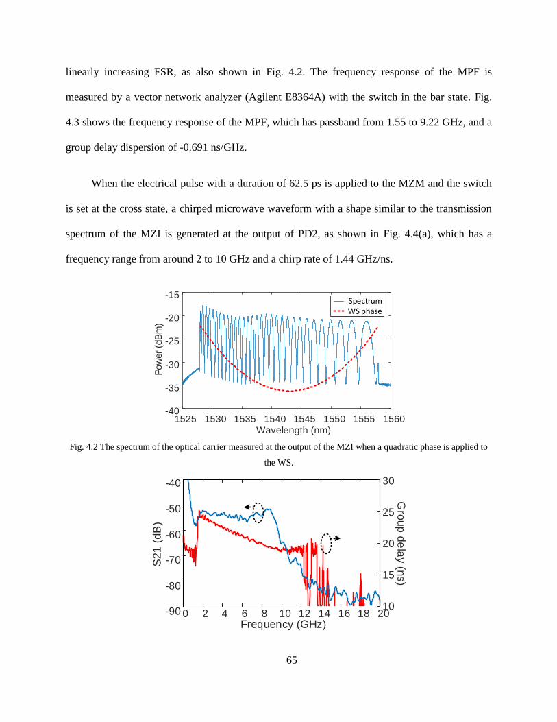
65
linearly increasing FSR, as also shown in Fig. 4.2. The frequency response of the MPF is
measured by a vector network analyzer (Agilent E8364A) with the switch in the bar state. Fig.
4.3 shows the frequency response of the MPF, which has passband from 1.55 to 9.22 GHz, and a
group delay dispersion of -0.691 ns/GHz.
When the electrical pulse with a duration of 62.5 ps is applied to the MZM and the switch
is set at the cross state, a chirped microwave waveform with a shape similar to the transmission
spectrum of the MZI is generated at the output of PD2, as shown in Fig. 4.4(a), which has a
frequency range from around 2 to 10 GHz and a chirp rate of 1.44 GHz/ns.
1525 1530 1535 1540 1545 1550 1555 1560Wavelength (nm)
-40
-35
-30
-25
-20
-15
Pow
er
(dB
m)
SpectrumWS phase
Fig. 4.2 The spectrum of the optical carrier measured at the output of the MZI when a quadratic phase is applied to
the WS.
Gro
up d
ela
y (n
s)
0 2 4 6 8 10 12 14 16 18 20Frequency (GHz)
-90
-80
-70
-60
-50
-40
S21
(dB
)
10
15
20
25
30

66
Fig. 4.3 The magnitude and group delay response of the MPF when a quadratic phase is applied to the WS.
We then configure the system to perform pulse compression. To do so, the switch is
changed to the bar state and the generated chirped microwave waveform is applied to the MZM
as a received signal. The chirped microwave waveform is then compressed by the matched filter.
A compressed pulse is measured at the output of PD1, as shown in Fig. 4.4(b), which has a
temporal width of 0.27 ns, corresponding to a compression ratio of 20.7 considering the duration
of the original pulse of 5.57 ns. Theoretically, perfect matched filtering can compress the chirped
pulse to a temporal width of 0.20 ns or a compression ratio of 27.9. The slightly poorer pulse
compression is caused by the limited bandwidths of the electro-optic components and the
measurement equipment, which makes the generated chirped microwave waveform slightly
different from an ideal waveform (smaller amplitude for the high frequency components). To
verify that the MPF is able to reject a microwave waveform that is different from the transmitted
waveform. Here, for simplicity, a different waveform is generated by simply disconnecting the
TRM, which is done by connecting PD2 directly to the output of the EDFA. In this case, the
microwave waveform generated at the output of PD2 is no longer a time reversed impulse
response of the MPF, but the impulse response itself h(t), as shown in Fig. 4.4(c), which should
not be compressed by the MPF. The signal at the output of PD1 when h(t) is applied to the MZM
and the switch is set at the bar state is shown in Fig. 4.4(d). No compressed pulse is observed,
which confirms that the MPF is a matched filter which is able to reject a microwave signal that is
different from the transmitted signal.
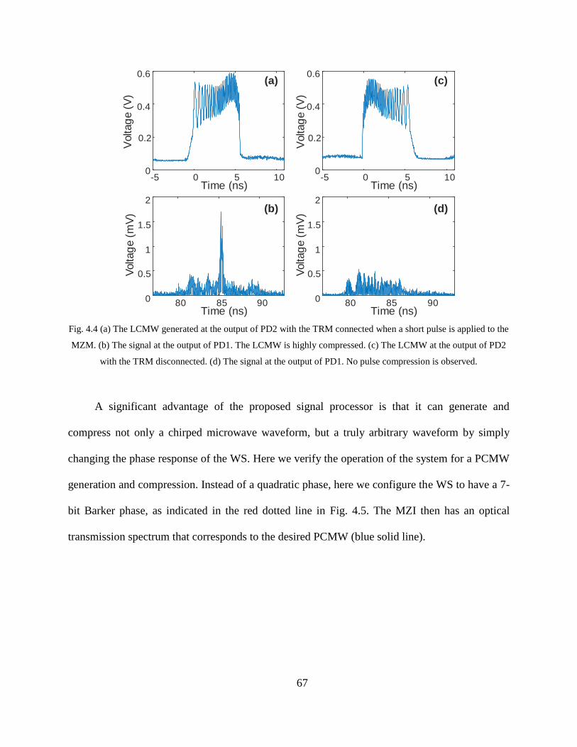
67
-5 0 5 10Time (ns)
Voltag
e (V
)
80 85 90Time (ns)
0
0.5
1
1.5
2
Voltag
e (m
V)
-5 0 5 10Time (ns)
Voltag
e (V
)80 85 90
Time (ns)
0
0.5
1
1.5
2
Voltag
e (m
V)
0.2
0
0.4
0.6
0.2
0
0.4
0.6(a) (c)
(b) (d)
Fig. 4.4 (a) The LCMW generated at the output of PD2 with the TRM connected when a short pulse is applied to the
MZM. (b) The signal at the output of PD1. The LCMW is highly compressed. (c) The LCMW at the output of PD2
with the TRM disconnected. (d) The signal at the output of PD1. No pulse compression is observed.
A significant advantage of the proposed signal processor is that it can generate and
compress not only a chirped microwave waveform, but a truly arbitrary waveform by simply
changing the phase response of the WS. Here we verify the operation of the system for a PCMW
generation and compression. Instead of a quadratic phase, here we configure the WS to have a 7-
bit Barker phase, as indicated in the red dotted line in Fig. 4.5. The MZI then has an optical
transmission spectrum that corresponds to the desired PCMW (blue solid line).

68
1525 1530 1535 1540 1545 1550 1555 1560Wavelength (nm)
-45
-40
-35
-30
-25
Pow
er
(dB
m)
0 0 0 0
SpectrumWS phase
Fig. 4.5 The spectrum of the optical carrier measured at the output of the MZI when a 7-bit binary phase code is
applied to the WS.
Fig. 4.6(a) shows the generated PCMW when a short electrical pulse is applied to the
MZM and that the switch is set at the cross state. The signal is measured to have a carrier
frequency of 4.08 GHz and a duration of 5.4 ns. The PCMW is then fed to the MZM and the
switch is set at the bar state. Fig. 4.6(b) shows the compressed pulse measured at the output of
PD1, in which a peak with a temporal width of 0.58 ns is observed. The compression ratio is
calculated to be 9.3. Theoretically, a perfect matched filter can compress the PCMW to a
temporal width of 0.42 ns or a compression ratio of 12.9. Again, the slightly poorer pulse
compression is caused by the limited bandwidths of the electrical components and the
measurement equipment. Similarly, here we also test the ability of the MPF to reject a signal that
is different from the transmitted signal. With PD2 connected to the EDFA directly, we get a
generated waveform which is shown in Fig. 4.6(c). The microwave waveform is then applied to
the MZM and the switch is set at the bar state. Fig. 4.6(d) shows the measured signal at the
output of PD1. No pulse compression is observed, which confirms again that the MPF is a
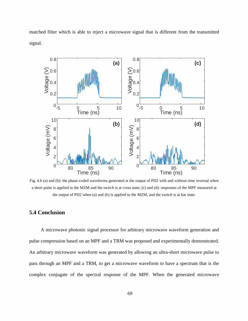
69
matched filter which is able to reject a microwave signal that is different from the transmitted
signal.
-5 0 5 10Time (ns)
0
0.2
0.4
0.6
0.8
Voltag
e (V
)
80 85 90Time (ns)
-5 0 5 10Time (ns)
0
0.2
0.4
0.6
0.8
Voltag
e (V
)
80 85 90Time (ns)
(a) (c)
(b) (d)
0
2
4
6
8
10
Voltag
e (m
V)
0
2
4
6
8
10
Voltag
e (m
V)
Fig. 4.6 (a) and (b): the phase-coded waveforms generated at the output of PD2 with and without time reversal when
a short pulse is applied to the MZM and the switch is at cross state; (c) and (d): responses of the MPF measured at
the output of PD2 when (a) and (b) is applied to the MZM, and the switch is at bar state.
5.4 Conclusion
A microwave photonic signal processor for arbitrary microwave waveform generation and
pulse compression based on an MPF and a TRM was proposed and experimentally demonstrated.
An arbitrary microwave waveform was generated by allowing an ultra-short microwave pulse to
pass through an MPF and a TRM, to get a microwave waveform to have a spectrum that is the
complex conjugate of the spectral response of the MPF. When the generated microwave

70
waveform was transmitted and received, by passing the received microwave waveform through
the same MPF, matched filtering was performed and the microwave waveform is compressed.
The proposed microwave photonic signal processor was verified by two experiments, in which a
7-bit PCMW with a carrier frequency of 4.08 GHz, and an LCMW with a bandwidth of 7.7 GHz
were generated and compressed. The durations of the generated LCMW and PCMW were 5.57
and 5.4 ns, respectively. The widths of the compressed pulses were 0.27 and 0.58 ns and the
pulse compression ratios were 20.6 and 9.3. The proposed microwave photonic signal processor
can find applications in radar systems to generate and compress wideband and high speed
microwave signals.

71
CHAPTER 5 TEMPORAL CONVOLUTION OF
MICROWAVE SIGNALS
Temporal convolution is another approach to realizing pulse compression, it can also find
other applications such as image deburring. The implementation of temporal convolution
between two signals requires a combination of time reversal, time delay, signal multiplication
and integration.
Based on the time reversal shown in Chapter 4, we propose and experimentally
demonstrate a photonic system that can perform temporal convolution calculation of two
microwave signals. The time reversal, multiplication and integration of the inputs signals are
based on existing optical signal processing techniques. A changing time delay between the two
input signals to be convolved is achieved by generating two sequences of replicas of the two
signals with two slightly different repetition rates. The convolution results for different input
signals are then derived at the output of a PD, which measures the energy of each pulse in a pulse
train. Since the convolution result is recovered from the energy of the pulses, a PD and a
sampling system with relatively small bandwidths will be sufficient to perform convolution
between two wideband signals.
5.1 Convolution Basics
In order to detect an instance of a reflected microwave pulse, a widely used analog
approach is to cross-correlate the received signal with the transmitted signal. Since the reflected
signal should have a similar shape with that of the transmitted signal, this approach can
essentially find out if there is a pattern that matches the transmitted waveform in the received
72
signal, which usually contains strong noise and interference. The cross-correlation is defined in
the time domain as
f g f t g t dt
(5-1)
which can be seen as the integration of the multiplication of two signals with a changing time
shift. If we compared it to the definition of convolution
f g f t g t dt
(5-2)
we notice the only difference is that convolution requires a time reversal of one of the two
signals. It is easy to understand, similar to convolution, cross-correlation of two signals in time
domain is equivalent to multiplying the spectrum of one signal with the complex conjugate of the
spectrum of the other signal. Using this concept, a microwave filter with a spectral response the
same as the complex conjugate of the spectrum of the reference (transmitted) signal is usually
designed and implemented on the received signal to achieve the signal cross-correlation. This
process is widely known as matched filtering, which can be realized using photonics but not
investigated extensively.
According to (5-2), temporal convolution can be calculated in the time domain by the
following three steps:
1) Time reversal of one of the input signal, g() for instance, to get g(-);
2) Multiplying f() and a time-delayed g(t-);
73
3) Integration of the multiplication result, which gives the convolution result for a certain
time delay t.
To get a full convolution result, the steps 2) to 3) should be repeated with different time
delays t.
We propose and experimentally demonstrate a photonic system that can be used
simultaneously as a wideband microwave waveform generator and as a matched filter for the
detection of the generated microwave waveform. The matched filter is realized with a broadband
optical source (BOS), an optical interferometer and a dispersive element. The wideband
microwave signal is generated by temporally reversing the impulse response of the matched filter,
so that the frequency response of the matched filter is always conjugate to the spectrum of the
generated waveform, no matter what kind of wideband signal is generated. A linearly chirped
microwave signal and phase-coded signal are used to test the system. An operation bandwidth as
large as 7.7 GHz is demonstrated for a waveform with a duration of 5.57 ns.
5.2 Experimental Implementation
Fig. 5.1(a) shows microwave temporal convolution for two input microwave signals of f(t)
and g(t), which involves three operations, microwave time reversal, multiplication and
integration. The three operations can be performed using three subsystems in the optical domain,
as shown in Fig. 5.1(b). The first subsystem is used for achieving time reversal, which is similar
to the approach we introduced in [101], where a mode-locked laser (MLL) is employed to
generate a transform-limited pulse train. An optical pulse in the pulse train is first reflected by an
LCFBG (LCFBG1) through an OC (OC1), and then spectrally shaped by a programmable optical

74
filter (POF), to encode a microwave waveform to make the spectral response of the POF have a
shape that is identical to the microwave waveform. The second subsystem is for achieving
multiplication, which is implemented by simply using an MZM, to which a second microwave
signal is applied via its electrical port. The integration is performed by a third subsystem that
consists of a second LCFBG (LCFBG2) and a low-speed PD. Since the input signals are faster
than the response time of the PD, the output of the PD is in fact proportional to the optical energy
that it receives within its response time window, i.e., the integration of the power of the fast input
signal. To get the integration for the amplitude of the signals as indicated in (5-2), the input
signals f(t) and g(t) should be preprocessed to have only positive values, and then converted to
f t and g t . Note that if the integration is performed in the optical domain (without
photo-detection), the preprocessing is not needed. In the following, for simplicity, assume we
have two input signals given by f t and g t .
Time reversal
Multiplication Integration
MLL POF
PBS
OC1
OC2
LCFBG1
PC3
PC2PC1
12
3
41
23
EDFA
MZM PD
Time
reversal
Multipli-cation
Integration
OC3
LCFBG2 g t
g t
f t
*gt f t g t
(a)
(b)
f t
Fig. 5.1 (a) Illustration for the operation of the proposed temporal convolution system; (b) Schematic diagram of the
temporal convolution system consisting of three sub-systems. MLL: mode-locked laser; OC: optical circulator; POF:
programmable optical filter; LCFBG: linearly chirped fiber Bragg grating; PC: polarization controller; PBS:
polarization beam splitter; EDFA: erbium-doped fiber amplifier; MZM: Mach-Zehnder modulator; PD:
photodetector.
75
For a microwave signal g t , the POF can be configured to have a spectral response that
has the same shape as the microwave signal, g , where is the optical angular frequency
given by /t and is the dispersion coefficient of LCFBG1 when looking into it from the
left end [70]. The spectrum is linearly mapped to the time domain through wavelength-to-time
mapping at LCFBG1 from the left end [70]. After reflected by LCFBG1 the second time from its
right side, wavelength-to-time mapping is performed and a time-reversed microwave signal
g t is obtained [101]. Note that the dispersion coefficient of LCFBG1 when looking into it
from the right end is . g t can also be encoded to a pulse in the pulse train with the
temporal pulse shaping approach [70], where an MZM is used instead of the POF, but the
microwave signal applied to the MZM must be synchronized to the pulse in the pulse train. The
two techniques are equivalent. Here we choose the wavelength-to-time mapping approach using
a POF as it does not require any synchronization between the waveform from the MLL and the
waveform from an AWG, thus it is simpler experimentally. Although g t can be generated
by letting the MLL pulse reflected only once by the left end of LCFBG1 after been filtered by
the POF, we used the LCFBG1 three times as it is the configuration that can also perform time
reversal of a signal encoded using the temporal pulse shaping approach. Three PCs are used to
ensure that the pulse can be reflected by LCFBG1 via the right end twice and to achieve a
maximum coupling efficiency [101]. Since the spectral response of the POF is not updated on a
pulse-by-pulse basis [72], g t is repeating at a repetition rate identical to that of the pulse
train from the MLL. An EDFA is used after the time reversal subsystem to compensate for the
losses of the POF, the PBS, and LCFBG1.

76
The amplified pulses in the pulse train encoded by g t are then sent to the
multiplication subsystem, which is simply the MZM. The second microwave signal to be
convolved, f t , is generated by the AWG with a repetition rate slightly different from that of
the pulse train from the MLL, and is applied to the MZM. The multiplied signal at the output of
the MZM is then launched into LCFBG2 for integration. LCFBG2 has a dispersion coefficient
that is identical to that of LCFBG1 when looking into it from the left end. The signal at the
output of LCFBG2 is converted to the electrical domain at the PD. Integration will be performed
at the same time thanks to the small bandwidth of the PD.
To illustrate the operation of the system, the convolution between a rectangular waveform
f(t) and an inverse sawtooth waveform g(t) is used as an example, as shown in Fig. 5.2. First,
f t and g t are generated with a repetition rate of T1 and T2, respectively. There is a
slight difference of t between T1 and T2. Due to the difference between the repetition rates of
the two signals, a changing time delay difference can be achieved between the replicas of
f t and g t after a different number of periods n. The two signals are then multiplied
and integrated. The output of the integration subsystem is a series of short pulses with different
peak powers. The convolution result I’(n) can be reconstructed from the amplitudes of the peaks.
Note that I’(n) is the integration of the n-th pulse in the pulse train. Therefore, it is discrete, and
the corresponding unit time increase along the horizontal axis is 1 2T T for the convolution
result.

77
Reconstructed
convolution result
t 2t 3t
T1
T2
1I n 1I n
g t
f t
2f t g t t
2f t g t t dt
I n
Fig. 5.2 Operation principle of the proposed temporal convolution system. A rectangular waveform f(t) and a
sawtooth waveform g(t) are used as the two signals to be convolved.
Mathematically, a time reversed signal on an optical pulse at the output of the time reversal
subsystem (port 4 of OC2) can be expressed as [101],
2
exp2
i
jtr t g t
(5-3)
where g t is seen as the pre-processed input microwave signal. The quadratic phase term in
(5-3) is induced by LCFBG1, which will be eliminated at the PD after photo-detection.
Considering that the time-reversed microwave signal is carried by the optical pulse train, we
have
1 1
1 1
0 0
N N
i i
n n
r t r t t nT r t nT
(5-4)
78
where is the Dirac delta function, 1T is the period of the pulse train from the MLL, n is an
integer and 1 21N T T . Similarly, the other pre-processed microwave signal, f t , is
repeating at a slightly different repetition rate with a period of 2T . The signal applied to the
MZM is expressed as
1
2
0
N
n
s t f t nT
(5-5)
The two signals r(t) and s(t) are then multiplied at the MZM. The time intervals T1 and T2
are chosen to be much larger than the temporal duration of the input waveforms to avoid
overlapping between any two adjacent waveforms, and the difference between T1 and T2 is
chosen to be small, so that we only need to consider the terms with the same value of n in (5-4)
and (5-5) to overlap in time within the summation range of N-1, i.e., the multiplication will only
take place for the terms with the same value of n. At the output of the MZM, the signal can be
expressed as
1 2n im t r t nT f t nT (5-6)
The time delay difference between nr t and 2f t nT is 2 1n T T . As n changes, a
different time delay difference between the two waveforms is resulted, which is required by the
temporal convolution.
The multiplication output is then directed to LCFBG2 for the first step of the integration
operation. After propagating through LCFBG2 with a dispersion coefficient of , which is

79
identical to that of LCFBG1 when looking into it from the left end, we obtain the output signal as
a convolution between nm t and the impulse response of LCFBG2, given by
2
exp2
n
jty t m t
(5-7)
By using the wavelength-to-time mapping relationship [70], we get
2
exp2
n
jty t F m t
(5-8)
where F denotes Fourier transform. The signal is then detected at the PD, which is the second
step of the integration operation, generating an output current given by
2
22
2
exp2
n
t
n t
I t y t
jtF m t
F m t
(5-9)
where is the responsivity of the PD. It can be seen that the signal at the output of the PD is
actually the power spectrum of the multiplication result in (5-6), rather than its integration.
However, it should be noted if the bandwidths of the input signals are small compared to the
optical carrier frequency, I(t) becomes a very short optical pulse with a pulse width given by
t , where is the electrical bandwidth of the multiplication result in(5-6). If t is
smaller than the response time of the PD, the output current will be proportional to the energy of
a pulse, which is the integration of the pulse spectrum, thus we have

80
22
nI n y t dt F m t d
(5-10)
According to the Parseval’s theorem, for each pulse, we have the output given by
21
2n
t
I n m t dt
(5-11)
Substitute (5-3) and (5-6) into(5-11), we get
1 2
1
2t
I n g t nT f t nT dt
(5-12)
Compare (5-12) with(5-2), I n can be seen as the convolution between signals g(t) and
f(t), with a time delay difference of 2 1n T T . For a different n, the convolution result provides
a value corresponding to a different time delay difference. It can be seen that the convolution
process imposes strong requirement for the period of the two signals to be convolved. However,
a fiber optic loop may be used to convert a pulsed signal into a periodic signal with a repetition
rate determined by the loop length. Convolution can then be performed between a periodic signal
and a non-periodic signal.
In the proposed system, the PD is used to measure the energies rather than the temporal
shapes of the pulses, thus the required bandwidth can be much smaller than the bandwidths of
the input signals. In fact, it is only required that the response time of the PD is faster than 1T and
2T . It is also required that the response time is slower than the duration of the pulses that arrive
at the PD. If these two requirements are satisfied, integration can be realized without the use of

81
LCFBG2. Unfortunately, the pulse duration, which is the duration of f t and g t
without using LCFBG2, is comparable to 1T and 2T . A practical PD may not satisfy the
response time requirement, considering that a steep slope is difficult to achieve at the cut-off
frequency of a PD or even that of an electrical filter. The use of LCFBG2, which reduces the
duration of the pulses that arrive at the PD, significantly increases the high frequency limit of the
PD and allows the implementation of temporal convolution with a practical PD.
The preprocessing that converts the input signals to their square roots is required since the
final step of integration is realized by the small-bandwidth PD, and the signal at the output of the
PD, which is in the electrical domain, is proportional to the power of the input optical signal. If
an all-optical integrator is implemented instead, the preprocessing will not be needed.
5.3 Experimental Evaluation
An experiment based on the system shown in Fig. 5.1 is performed. A wavelength tunable
MLL (PriTel FFL-1550-20) is used as the optical source, which generates an optical pulse train
with a repetition rate of 20 MHz or a period of 50 ns. The 3-dB spectral width and temporal
width of a pulse in the pulse train is 8 nm and 600 fs, respectively. LCFBG1 and LCFBG2 are
fabricated to have an identical bandwidth of 4 nm and a dispersion coefficient of ±2500 ps/nm. A
POF (Finisar WaveShaper 4000s) is used to encode one of the input signal to the MLL pulses.
The other input signal is generated by an AWG (Tektronix AWG7102) with a sampling rate of
10 Gb/s and applied to an 10-GHz MZM (JDS-U OC-192) to perform signal multiplication. The
AWG is configured to generate a waveform with a period 1% longer than that of the pulse train

82
from the MLL, i.e., 50.5 ns. The convolution result at the output of the PD (New Focus 1414, 25
GHz) is sampled by a real-time oscilloscope (Agilent 93204A).
The POF has a spectral resolution of 10 GHz, which can generate g t at an equivalent
sampling rate of 5 Gb/s when working in conjunction with LCFBG1. Hence, both f(t) and g(t)
have an analog bandwidth of less than 5 GHz [70]. According to (5-9), the pulse width is around
200 ps after integration, which is larger than the response time of the PD and that of the
oscilloscope. To satisfy the condition given in (5-10), a digital low-pass filter with a cutoff
frequency at 1 GHz is adopted for the signal sampled by the oscilloscope. In fact, it is only
required that the PD has a response time faster than the period of the waveforms to be convolved,
which is 50 ns in our experiment. Although the system performs convolution for two signals with
relatively large bandwidths, only a low-speed PD and a low-speed sampling system are required
to acquire the convolution result, which can be a great advantage for the proposed system. It
should be noted that, each MLL pulse is temporally stretched to have a duration of 10 ns by
LCFBG1, indicating that the system can only process an input signal with a temporal duration
less than 10 ns.
Then, we use different waveform pairs to test the operation of the proposed temporal
convolution system. The waveform pairs include two rectangular waveforms, a rectangular
waveform and an inverse sawtooth waveform, and an arbitrary waveform and a short pulse. Fig.
5.3 shows the two rectangular waveforms with temporal widths of 10 ns that are generated by the
POF and the AWG, respectively. Although a rectangular g() is applied to the POF, some
ripples can be found in the generated waveform shown in Fig. 5.3(a) due to the uneven optical
spectrum of the MLL pulse and the uneven gain spectrum of the EDFA. The rectangular

83
waveform generated by the AWG is very close to an ideal rectangular waveform. It is known
that the convolution of two rectangular waveforms with an identical temporal width is a
triangular waveform, and the rise time of the triangular waveform should be equal to the width of
one of the input rectangular waveform. Fig. 5.4 shows the experimentally obtained convolution
output (blue line). An ideal convolution result (red-dotted line) is also shown for comparison.
The output signal is a series of short pulses, with the peak amplitude profile nicely fiting to the
ideal convolution. It should be noted that two time scales for the horizontal axes are used in Fig.
5.4, where the lower horizontal axis represents the time for the measured output and the upper
horizontal axis represents the time for the convolution, which is recovered by using 2 1n T T
with n from 0 to N-1. As we have discussed, the convolution results are discrete values given by
the measured the energies of the pulses. The corresponding time axis should also be discrete,
with a unit time increment given by 2 1T T . In our case, 2 1 10.01T T T . The upper
horizontal axis corresponding to the convolution is simply obtained by multiplying the real time
in the lower horizontal axis by 0.01.
0 5 10 15 20 25 30Time (ns)
0
10
20
30
40
50
60
70
Volta
ge (
mV
)
0
0.1
0.2
0.3
0.4
0.5
Volta
ge (
V)
0 5 10 15 20 25 30Time (ns)
(a) (b)
Fig. 5.3 Two rectangular waveforms used as the input waveforms for temporal convolution. (a) Square root of g(t)
encoded by the POF. Blue line: the measured waveform at the output of the POF; red dotted line: an ideal
rectangular waveform. (b) Square root of f(t) generated by the AWG.

84
0 1 2 3 4 5-5
0
5
10
15
20
25
30
Time (s)
Volta
ge (
mV
)
6
0 10 20 30 40 50
ConvolutionTime (ns)
60
Fig. 5.4 The convolution between two rectangular waveforms. Red-dotted line: the theoretical convolution output of
the two rectangular waveforms with the upper horizontal axis; blue line: the measured convolution output with the
lower horizontal axis, which is a series of pulses with the peak amplitudes representing the convolution result.
An asymmetric waveform which is an inverse sawtooth waveform is then used to test the
temporal convolution system. Again, by configuring the POF to have a spectral response of
g , where g() has an inverse sawtooth shape, the square root of an inverse sawtooth
waveform with a temporal duration of 10 ns is obtained at the output of the time reversal
subsystem, as shown in Fig. 5.5(a). The waveform is then convolved with the rectangular
waveform shown in Fig. 5.3(b). Fig. 5.5(b) shows the convolution result. A good agreement
between the theoretical and the measured results is achieved. For convolution operation, we
know that f g g f , i.e., no matter which function is temporally reversed, the convolution
result should be the same. In our system, however, the convolution output may be temporally
reversed if a different input signal is temporally reversed. But the sign of 2 1T T will also be
changed for f g and g f . The time in the horizontal axis for convolution 2 1n T T will
then be reversed, which results in a consistent convolution results for both f g and g f .

85
0 5 10 15 20
20
40
60
80
100
120
140
160
Time (s)
Volta
ge (
V)
0 1 2 3 4 5
0
10
20
30
40
Time (s)
Vo
lta
ge
(m
V)
0 10 20 30 40 50Convolution Time (ns)
(a) (b)
Fig. 5.5 (a) The square root of an inverse sawtooth waveform achieved at the output of the POF; (b) the convolution
between a rectangular waveform and an inverse sawtooth waveform. Red dotted line: the theoretical convolution
output of a rectangular waveform with an inverse sawtooth waveform, blue line: the measured convolution output of
the system.
0.25 0.5 0.75 1 1.25 1.5
0
20
40
60
80
100
120
Time (s)0
Volta
ge (
mV
)
2.5 5 7.5 10 12.5 150
Convolution Time (ns)
(b)
0
0.1
0.2
0.3
0.4
0.5
Volta
ge (
V)
0 5 10 15Time (ns)
(a)
Fig. 5.6 (a) The square root of a short pulse achieved at the output of the POF (red) and the square root of a three-
cycle chirped waveform generated by the AWG (blue); (b) the convolution between a three-cycle chirped waveform
and a short pulse. Red line: theoretic convolution result; blue line: the output of the convolution system, when the
three-cycle chirped waveform is convolved with a short pulse with a temporal width of 400 ps.
Finally, we investigate the convolution between a complex waveform and a short pulse.
The complex waveform is a three-cycle chirped waveform, which is generated by the AWG. The
POF is configured to have a narrow passband of 20 GHz which leads to the generation of a short

86
pulse with a temporal width of 400 ps after wavelength-to-time mapping by LCFBG1. The
generated square root of the three-cycle chirped waveform and the short pulse are shown in Fig.
5.6(a). The convolution of a waveform and an ultra-short pulse (ideally a unit impulse function)
should be the waveform itself. Fig. 5.6(b) shows the ideal convolution result and the measured
convolution output of the system. Note that the vertical axis does not represent the actual voltage
level of the three-cycle chirped waveform generated by the AWG, which has a peak voltage of
0.5 V (refer to Fig. 5.3(b)). Again, the measured result is in good agreement with theoretical
result. For a complex waveform with more details, to get a more smooth convolution result, one
may use a smaller value of 2 1T T , so that the convolution can be calculated with a higher time
resolution.
5.4 Conclusion
We have proposed and experimentally demonstrated a photonic system that can perform
temporal convolution of two microwave waveforms, which was realized by three photonic
subsystems to perform the time reversal, signal multiplication, and integration. The key
challenge in performing temporal convolution was to realize a variable time delay difference
between the two microwave waveforms, which was achieved by generating two sequences of
replicas of the two microwave waveforms with two slightly different repetition rates. The two
sequences were multiplied at the MZM and integrated by LCFBG2 followed by the photo-
detection at the PD, with the convolution result obtained at the output of a PD. Since the PD here
is used to detect the pulse energy, a small bandwidth of the PD will be sufficient to perform the
proposed temporal convolution in which the two microwave waveforms could be wideband. The

87
proposed approach was experimentally evaluated, in which the calculations of three temporal
convolutions between two rectangular waveforms, between an inverse sawtooth waveform and a
rectangular waveform, and between an arbitrary waveform and a short pulse were experimentally
demonstrated.

88
CHAPTER 6 TIME STRETCHED SAMPLING BASED
ON A DISPERSIVE LOOP
The ever-increasing bandwidth of modern microwave sensing and communications
systems has led to new challenges on signal processors to operate at a very high sampling rate.
Using conventional sampling techniques may not be able to meet the demand. To realize
broadband sampling, the optical time-stretched sampling has been considered an effective
solution. So far, the TBWP and the stretching factor of a time-stretched sampling system are
mainly limited by the maximum available dispersion coefficient of the DDL used to perform
time stretching.
In this Chapter, we propose a novel technique to achieve time-stretched microwave
sampling with a significantly increased stretching factor. In the proposed system, a microwave
waveform is modulated on a pre-dispersed optical pulse which is sent to a recirculating
dispersive loop consisting of an LCFBG and an EDFA. The LCFBG is used to achieve repetitive
pulse stretching and the EDFA is used to compensate for the loss in the loop. By controlling the
gain of the EDFA to compensate for the loop loss, the optical waveform can recirculate in the
loop and a repetitive use of the LCFBG for accumulated pulse stretching is realized. The
proposed technique is experimentally demonstrated. An LCFBG with a GDD coefficient of 1500
ps/nm is fabricated and incorporated in the recirculating dispersive loop. An equivalent GDD
coefficient of 12000 ps/nm is achieved, which, to the best of our knowledge, is the largest
dispersion ever reported for time-stretched sampling. The corresponding stretching factor is 36.
The use of the system to sample a microwave waveform is demonstrated. For a sampling system
with a bandwidth of 32 GHz, the use of the proposed recirculating dispersive loop can extend the

89
bandwidth by 36 times or 1.15 THz (or a time resolution of 347 fs) with a frequency resolution
of 4.93 GHz.
6.1 Operation Principle
The schematic of the proposed time stretched sampling system is shown in Fig. 6.1. An
optical pulse from an MLL is sent to a DCF serving as a pre-dispersion element. The pre-
dispersed optical pulse is then sent to an MZM through an optical bandpass filter (OBPF) and an
EDFA (EDFA1). A microwave waveform is modulated on the pre-dispersed optical pulse at the
MZM. The modulated signal is then sent to the recirculating dispersion loop, in which an
LCFBG and a second EDFA (EDFA2) are incorporated. Note that the bandwidth of the OBPF is
identical to the bandwidth of the LCFBG, so the pre-dispersed optical pulse at the output of the
OBPF has a spectral width that is identical to that of the LCFBG. The microwave waveform to
the MZM is generated by mixing an electrical gate signal from an AWG with a sinusoidal
microwave signal from a microwave generator (SG). The modulated waveform is launched into
the recirculating dispersive loop through a 2×2 3-dB coupler. In the loop, the LCFBG is used as
a dispersive element and EDFA2 is used to compensate for the round-trip loss. An attenuator
(Att) is also included in the loop to provide a fine control of the loop gain, to maintain a full
compensation of the loss while avoiding optical lasing in the loop. The optical pulse is
recirculating in the dispersive loop. The time-stretched optical pulse at the output of the loop is
sent to a PD. The stretched microwave waveform is sampled by a real-time oscilloscope.

90
MLL MZM PDOBPF
EDFA2
DCF
2X2 coupler
LCFBG
EDFA1ATT
Mixer
OSC
1
2
3DC bias
SynchronizationAWG SG
Fig. 6.1 Schematic of the time stretched sampling system. MLL: mode locked laser, OBPF: optical bandpass filter,
MLL: mode-locked laser, DCF: dispersion compensating fiber, EDFA: erbium-doped fiber amplifier, MZM: Mach-
Zehnder modulator, ATT: attenuator, LCFBG: linear chirped fiber Bragg grating, PD: photodetector, AWG:
arbitrary waveform generator, SG: signal generator, OSC: oscilloscope.
It is known that an LCFBG has a quadratic phase response within its passband. Its transfer
function can be written as [147]
2exp2
CLCFBGH j
(6-1)
where is the optical angular frequency and C is the GDD coefficient of the LCFBG (in ps2).
Assuming that the optical spectrum at the input of the dispersive loop is iE , the output
spectrum after recirculating for N round trips in the loop can be written as
1
( ) 2,
2
N
N N N
o iE g E H
(6-2)

91
where g is the net gain of the loop, which can be changed by tuning the gain of EDFA2 or the
loss of the attenuator. If we make g close to but slightly less than 2 , we then have
2 / 2 1N
g . The transfer function of the loop can be expressed as
( )
22exp
2 2
N
o Cloop
i
E NH j
E
(6-3)
By comparing Eqs. (6-1) and (6-3), we can see that the recirculating dispersive loop acts as
a dispersive element that has an equivalent GDD coefficient of CN . It should be noted that, the
ripples in the group delay of the LCFBG will also be magnified when a pulse recirculates for
more round trips. It is preferable that an LCFBG to be used in a dispersive loop has a group
delay ripple N times as small as a single time used LCFBG.
In (6-2), 2 / 2g should always be smaller than unity to prevent the loop from lasing. As a
result, the amplitude of loopH should decay with the increase of N. The maximum number of
N is determined by the minimum SNR required to detect the time-stretched signal. If the 2×2
coupler is replaced by an optical switch, then the number of round trips can be controlled by the
optical switch. In this case, the equivalent GDD coefficient of the recirculating dispersive loop
can be tunable by letting the waveform recirculate in the loop for a certain number of round trips.
The stretching factor of the time stretched sampling system is given by
1 C DM N (6-4)
92
where D is the GDD coefficient of the pre-dispersion element. Since the second term in Eq. (6-4)
is much greater than 1, it can be seen that the stretching factor increases proportionally to the
number of the round trips N. Again, if an optical switch is employed in the system, the stretching
factor can then be adjusted to improve the performance of the sampling system according to the
frequency band of the input waveform. For example, N should be large for a fast microwave
waveform so that all the details of the microwave waveform can be revealed, while for a
relatively slow microwave waveform, N should be small to avoid over sampling and data
redundancy [47, 48].
6.2 Experimental Implementation
An experiment based on the setup shown in Fig. 6.1 is performed. In the experiment, the
MLL (IMRA femtolite 780) with a repetition rate of 48 MHz and a central wavelength of 1558
nm is employed to produce an optical pulse train. An individual pulse in the pulse train is nearly
transform-limited with a 3-dB spectral bandwidth of 8 nm. The pre-dispersion element is a DCF
with a dispersion coefficient of C=432 ps2 (or -339 ps/nm). The LCFBG used in the dispersive
loop has a dispersion coefficient of C=1912 ps2 (or -1500 ps/nm) within a reflection passband of
0.6 nm centered at 1558 nm. The OBPF (Finisar WaveShaper 4000S) is configured to have a
near rectangular passband with a bandwidth identical to that of the LCFBG. It can be calculated
that, after the pre-dispersion by the DCF and the filtering by the OBPF, the MLL pulse is
stretched to have a time duration of 203 ps . The optical pulse train at the output of the
OBPF is amplified by EDFA1 and sent to the MZM. The MZM has a bandwidth of 20 GHz and
is biased at its minimum transmission point. A microwave waveform generated by mixing an 18-

93
GHz microwave signal from the SG with a rectangular pulse train with a repetition rate of 286
kHz serving as a gate signal from the AWG is applied to the MZM. The repetition rate of the
rectangular pulse train is smaller than that of the MLL (48 MHz) to reduce the duty cycle of the
modulated optical pulse train, thus allowing pulse stretching with a large stretching factor
without creating overlap between adjacent pulses. Note that in the experiment, the AWG and the
MLL are synchronized. The modulated optical waveform at the output of the MZM is sent to the
recirculating dispersive loop via the 2x2 coupler. The length of the recirculating dispersive loop
is estimated to be 61 m (corresponding to a time delay of 305 ns). The time stretched optical
pulse from the recirculating dispersive loop is sent to the PD (25-GHz, New Focus). The
electrical waveform at the output of the PD is sampled by a real-time oscilloscope (Agilent DSO-
X 93204A).
The modulation process is depicted in Fig. 6.2. As can be seen from Fig. 6.2(a) the gate
signal with a repetition rate of 286 kHz and a gate duration of 20.8 ns is mixed with the 18-GHz
microwave generated by the SG and sent to the MZM. Since the MZM is biased at its minimum
transmission point, the pre-dispersed pulse train corresponding to the low voltage level of the
modulation waveform will not be able to pass through the MZM, and the pre-dispersed pulse
train corresponding to the high voltage level of the modulation waveform is modulated by a
microwave waveform with twice the frequency of the microwave signal generated by the SG (i.e.,
36 GHz), as shown in Fig. 6.2(b). Therefore, the number of microwave cycles in each MLL
pulse is 7. In addition, there will be only one MLL pulse that is modulated by the microwave
waveform in every period of the gate. The resulting pulse train with a reduced repetition rate is
illustrated in Fig. 6.2(c). It should be noted that, for practical applications, one can use an MLL
with a lower repetition rate so that the gate signal is not needed. Then, the MZM can be biased at
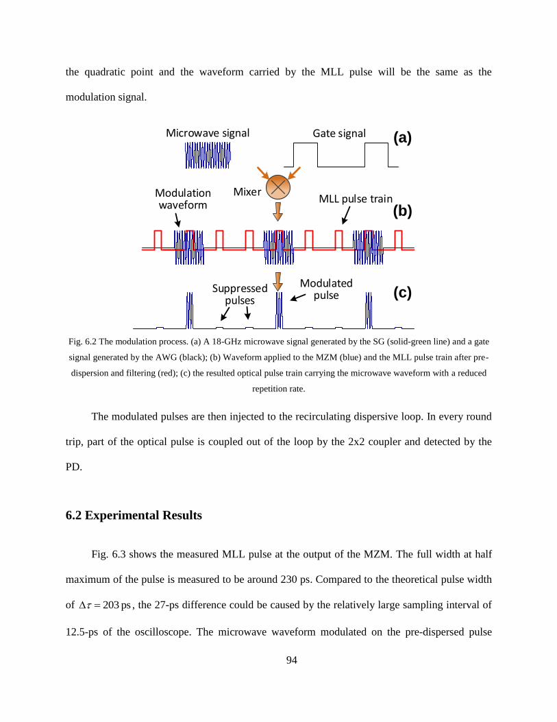
94
the quadratic point and the waveform carried by the MLL pulse will be the same as the
modulation signal.
Microwave signal Gate signal
MixerMLL pulse trainModulation
waveform
Suppressed pulses
Modulated pulse
(a)
(b)
(c)
Fig. 6.2 The modulation process. (a) A 18-GHz microwave signal generated by the SG (solid-green line) and a gate
signal generated by the AWG (black); (b) Waveform applied to the MZM (blue) and the MLL pulse train after pre-
dispersion and filtering (red); (c) the resulted optical pulse train carrying the microwave waveform with a reduced
repetition rate.
The modulated pulses are then injected to the recirculating dispersive loop. In every round
trip, part of the optical pulse is coupled out of the loop by the 2x2 coupler and detected by the
PD.
6.2 Experimental Results
Fig. 6.3 shows the measured MLL pulse at the output of the MZM. The full width at half
maximum of the pulse is measured to be around 230 ps. Compared to the theoretical pulse width
of 203 ps , the 27-ps difference could be caused by the relatively large sampling interval of
12.5-ps of the oscilloscope. The microwave waveform modulated on the pre-dispersed pulse

95
cannot be correctly sampled since the doubled microwave frequency of 36 GHz exceeds the
highest frequency of the oscilloscope.
-0.8 -0.6 -0.4 -0.2 0 0.2 0.4 0.60
10
20
30
40
50
60
70
Time (ns)
Vo
lta
ge (
mV
)
0.8
Fig. 6.3 The waveform of the modulated MLL pulse measured at the output of the MZM.
-1 0 1 2 3 4 5 6 70
50
100
150
200
Time (s)
Vo
ltag
e (
mV
)
Original pulse
1 round trip
2 round trips
3.5 µs
308 ns
Fig. 6.4 Measured optical waveform at the output of the recirculating dispersive loop.
The waveform at the output of the dispersive loop is then measured by the real-time
oscilloscope, as shown in Fig. 6.4. As can be seen when a modulated optical waveform is
launched into the recirculating dispersive loop, a pulse burst with a decaying amplitude is
generated. The quick decay in amplitude is due to the loss in the loop. To avoid lasing in the loop
the gain of EDFA2 is controlled smaller than the loss. The time duration between two adjacent

96
pulses is 308 ns, which corresponds to the time delay of the recirculating dispersive loop. The
time duration between two large pulses is 3.5 µs, corresponding to the repetition time of the
optical pulse train at the output of the MZM.
Theoretically, the decaying can be reduced by increasing the loop gain. However, due to
the uneven magnitude response of the LCFBG and the uneven gain spectrum of EDFA2, the
recirculating dispersive loop may start lasing at certain wavelength when the loop gain is
increased, while at the other wavelengths, the loop gain is still smaller than 1. The relatively high
noise floor is mainly caused by the amplified spontaneous emission of EDFA2 and the
occasional lasing of the loop as the loop gain is very close to 1 at some wavelengths. To increase
the SNR of the system, a LCFBG with specially design amplitude response or an EDFA gain
flattening filter should be included in the loop to avoid lasing. One may also use an optical
switch to replace the optical couple, so that the loop loss can be reduced, and a lower gain for
EDFA2 will be required.
The detailed waveforms after the pulse is stretched in the recirculating dispersive loop for
1 to 8 round trips are shown in Fig. 6.5(a)-(h). After one round trip, the pulse duration is
stretched to around 1 ns and all the seven microwave cycles with a temporal separation between
two adjacent cycles of around 140 ps can be identified, as shown in Fig. 6.5(a). The optical pulse
is stretched with a stretching factor of around 5.

97
306 307 308 309 31010
30
50
Time (ns)
Vo
lta
ge
(m
V) (a)
613 614 615 616 617 618
20
30
Time (ns)
Vo
lta
ge
(m
V) (b)
(c)
921 922 923 924 925 92610
20
30
Time (ns)
Vo
lta
ge
(m
V) (d)
1225 1230 1235
15
20
25
Time (ns)
Vo
lta
ge
(m
V)
(e)
1535 1540 1545
15
20
25
Time (ns)
Vo
lta
ge
(m
V)
1840 1845 1850 185512
16
20
24
Time (ns)
Vo
lta
ge
(m
V) (f)
2455 2460 2465 2470
14
16
18
Time (ns)
Vo
lta
ge
(m
V (h)
2150 2155 2160
14
18
22
Time (ns)
Vo
lta
ge
(m
V) (g)
Fig. 6.5 The output waveforms after different number of round trips. (a) 1 round trip, (b) 2 round trips, (c) 3 round
trips, (d) 4 round trips, (e) 5 round trips, (f) 6 round trips, (g) 7 round trips, and (h) 8 round trips. Note that the time
scale is 1 ns/div in (a) to (c), and 5 ns/div in (d) to (h).
Then, the optical pulse keeps on recirculating in the loop, with the stretched pulses shown
in Fig. 6.5(b)-(h). Since the round trip loss cannot be completely compensated by the gain of
EDFA2, and the amplified spontaneous emission of EDFA2 introduces a significant amount of
noise, the SNR drops after each round trip. By a fine control of the loop gain using the tunable
attenuator, we are able to make the pulse circulate for 8 round trips before it is fully imbedded in
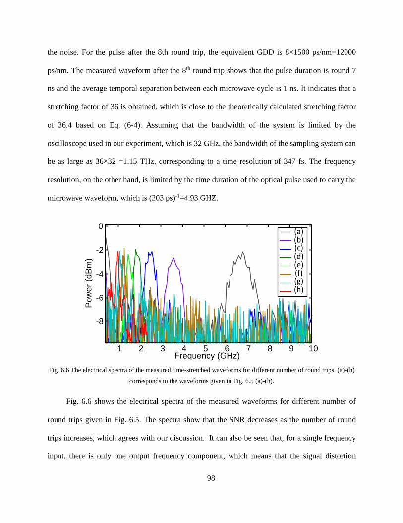
98
the noise. For the pulse after the 8th round trip, the equivalent GDD is 8×1500 ps/nm=12000
ps/nm. The measured waveform after the 8th round trip shows that the pulse duration is round 7
ns and the average temporal separation between each microwave cycle is 1 ns. It indicates that a
stretching factor of 36 is obtained, which is close to the theoretically calculated stretching factor
of 36.4 based on Eq. (6-4). Assuming that the bandwidth of the system is limited by the
oscilloscope used in our experiment, which is 32 GHz, the bandwidth of the sampling system can
be as large as 36×32 =1.15 THz, corresponding to a time resolution of 347 fs. The frequency
resolution, on the other hand, is limited by the time duration of the optical pulse used to carry the
microwave waveform, which is (203 ps)-1=4.93 GHZ.
1 2 3 4 5 6 7 8 9 10
-8
-6
-4
-2
0
Frequency (GHz)
Po
we
r (d
Bm
)
(a)(b)(c)(d)(e)(f)(g)(h)
Fig. 6.6 The electrical spectra of the measured time-stretched waveforms for different number of round trips. (a)-(h)
corresponds to the waveforms given in Fig. 6.5 (a)-(h).
Fig. 6.6 shows the electrical spectra of the measured waveforms for different number of
round trips given in Fig. 6.5. The spectra show that the SNR decreases as the number of round
trips increases, which agrees with our discussion. It can also be seen that, for a single frequency
input, there is only one output frequency component, which means that the signal distortion

99
effect usually encountered by a time-stretched system has a weaker effect compared to the SNR
deterioration, and is negligible.
6.3 Conclusion
A novel time-stretched sampling system with a large stretching factor has been
demonstrated by a repetitive use of an LCFBG in a recirculating dispersive loop. An equivalent
GDD as large as 12000 ps/nm with a large stretching factor of 36 was achieved. This is the 2nd
largest dispersion-based stretching factor for a time-stretched sampling system ever reported.
Although the stretching factor of 250 reported in [49] is much greater than the stretching factor
of 36 in this work, we have demonstrated a dispersive element with a greater dispersion than that
in [49]. If we use a pre-dispersion element that has a similar dispersion coefficient as the one in
[49], we would be able to achieve a much greater stretching factor than 250. Note that for pulse
stretching with a very large stretching factor, the input pulse applied to the MZM should be very
short, thus the system can only be able to sample a microwave waveform with a narrow width.
It should also be noted that the stretching factor can be further increased by using a low
noise optical amplifier. In addition, by flattening the magnitude response of the LCFBG and the
gain of EDFA2, the net gain in the loop can be controlled to be very close to 1 but with no lasing,
thus an input pulse can recirculate in the loop for more times, which would lead to a much
greater stretching factor. In [29], an MPF with an ultra-even magnitude response was used to
achieve pulse recirculation in an active cavity for 270 round trips. If this can be realized for a
wideband LCFBG, the equivalent GDD can be as large as 4.05×10⁵ ps/nm, which corresponds to
a stretching factor of 1195.

100
CHAPTER 7 LINEARLY CHIRPED MICROWAVE
WAVEFORM GENERATION
Microwave waveforms with a large TBWP have been widely employed in microwave
sensors, spread-spectrum communications, microwave computed tomography, and modern
instrumentation. Photonic generation of microwave signal, especially the one based on SS-WTT
mapping technique, has attracted increasing interests due to its ability to achieve a waveform
with a large bandwidth. However, the temporal duration of a signal generated using the SS-WTT
mapping technique is limited by the maximum available dispersion coefficient of the DDL used
to perform WTT mapping.
In this Chapter, a microwave waveform generator to generate an LCMW with an extended
temporal duration by a repetitive multi-time use of an LCFBG in a dispersive fiber-optic
recirculating loop that we demonstrated in the previous Chapter is proposed and experimentally
demonstrated. A comprehensive analysis is provided, which is then verified by more detailed
experiments. In addition to the increase in the temporal duration, we also demonstrate that the
central frequency of the generated LCMW can be tuned. In the proposed system, the spectral
shaper is a Fabry-Perot interferometer (FPI) incorporating two LCFBGs with complementary
chirps to form an FP cavity with a linearly decreasing or increasing FSR. The spectrum of an
ultra-short optical pulse is shaped by the FPI. The pulse is then directed into a dispersive loop
consisting of a third LCFBG. Since the optical pulse is temporally stretched multiple times when
reflected by the third LCFBG multiple times, an LCMW with an extended temporal duration that
exceeds the physical length of the third LCFBG can be generated. Note that although a similar
101
dispersive loop has been used in [24], it is for a different application where fast signal sampling
is implemented. The proposed technique is analyzed theoretically and validated experimentally.
7.1 Operation Principle
Fig. 7.1 shows the schematic diagram of the microwave waveform generation system. An
ultra-short optical pulse train is generated by an MLL source. A repetition-rate-reduction module
consisting of an MZM and an arbitrary waveform generator is used to realize the repetition rate
reduction of the pulse train to avoid the overlapping of adjacent pulses when temporally
stretched by the LCFBG in the dispersive loop. A gate signal is generated by an AWG with a
repetition rate equals to that of the repetition-rate reduced pulse train. The pulse train is then sent
via an OC (OC1) to an FPI formed by two complementary LCFBGs (LCFBG1 and LCFBG2),
which is used as the spectral shaper. An EDFA (EDFA1) is employed after the MZM to
compensate for the loss of the repetition-rate-reduction module. The pulse train is then launched
into a dispersive loop, in which a third LCFBG (LCFBG3) is incorporated via a second OC
(OC2). In the dispersive loop, a second EDFA (EDFA2) is employed to provide an optical gain,
followed by an attenuator (ATT) to balance the gain to be slightly less than 1 to avoid lasing.
The temporally stretched pulse is finally detected by a PD via a 2 x 2 optical coupler. An LCMW
with an extended temporal duration is obtained at the output of the PD.

102
MZM PD
EDFA2
2X2 coupler
LCFBG3
EDFA1
ATT
1
2
3
LCFBG1
1
2
3MLL
AWGLCFBG2
L
d
L
OC1
OC2Output
Syn
Fig. 7.1 Schematic diagram of the microwave waveform generation system. Syn: synchronization; MLL: mode-
locked laser; AWG: arbitrary waveform generator; MZM: Mach-Zehnder modulator; OC: optical circulator;
LCFBG: linearly chirped fiber Bragg grating; ATT: attenuator; EDFA: erbium-doped fiber amplifier; PD:
photodetector.
Assuming that the dispersion coefficients of LCFBG1 and LCFBG2 are, respectively, 1
and 1 -when looking into from the 2nd port of OC1, the cavity length of the FPI for a light
wave with an angular frequency of is given by [27]
12 2 s
eff eff
c cL d d
n n
(7-1)
where is the time delay caused by LCFBG1 and LCFBG2 for a light wave with an angular
frequency of resonating in the FPI; c is the light velocity in vacuum; effn is the effective
refractive index of the optical fiber; s denote the lowest optical angular frequencies within the
reflection bands of LCFBG1 and LCFBG2.
The FSR of the FPI can then be calculated by
1
2
2 2FSR
eff eff s
c c
n L n d c
(7-2)

103
Since both LCFBG1 and LCFBG2 are fabricated with low reflectivities, the reflection
spectrum of the FPI should have an interference pattern within the reflection spectrum of
LCFBG1 and LCFBG2. A simulated spectrum of an FPI formed by two identical LCFBGs, with
an identical reflectivity of 10% and a bandwidth of 4 nm centering at 1551 nm, is given in Fig.
7.2. For comparison, an ideal linearly chirped sinusoidal function is also shown (in log scale). It
can be seen that such an FPI has a spectral response that is similar to the shape of a sinusoidal
function with an increasing period (or FSR) given by (7-2). The spectral response of the FPI can
thus be written as
2
1 1
2sin
2sin 4 4
FSR
eff
s
R
n d
c
(7-3)
where is an initial phase that will be interpreted as a microwave phase in the generated
waveform. It can be seen from (7-2) and (7-3) that the FSR of the FPI is linearly increasing or
decreasing, depending on the sign of 1 .
After spectral shaping by the FPI and amplification by EDFA1, the spectrally shaped pulse
is directed into the dispersive loop via the optical coupler. It has been theoretically proved in the
previous Chapter that the dispersive loop has an equivalent dispersion coefficient of 3N thanks
to the multi-time use of LCFBG3, where 3 and N are the dispersion coefficient of LCFBG3
and the round trip number that the optical pulse travels in the loop, respectively. If the gain of
EDFA2 can be controlled to fully compensate for the round-trip loss of the dispersive loop, N

104
can be an extremely large number, which would result in a very large equivalent dispersion
coefficient and hence allowing a highly extended temporal duration for the generated LCMW.
1548 1549 1550 1551 1552 1553 1554 1555-25
-20
-15
-10
-5
Wavelength (nm)
Pow
er
(dB
m)
Fig. 7.2 Simulated reflection spectrum of an FPI formed by two LCFBGs with complementary dispersion (blue).
The central wavelength and bandwidth of the two LCFBGs are 1551 nm and 4 nm. They are fabricated to have a
uniform reflectivity of 10% and physically separated by 2 mm. The red dotted line is an ideal LCMW.
When the pulse recirculates in the loop, WTT mapping is performed. After N round trips,
the electrical field at the output of the dispersive loop is given by [70]
3
2
3
1exp
2 t
N
y t j t XN
(7-4)
where X G R is the optical spectrum of the pulse after spectrally shaped by the
FPI, and G is the spectrum of a pulse from the MLL. In our case, the bandwidth of the pulse
from the MLL is significantly larger than that of the optical spectral shaper, we can let 1G
for simplicity. In addition, the phase term in (7-4) will be eliminated by photo-detecting at a PD.
Substituting (7-3) into (7-4), we get

105
1 21
2 2
3 3
2 4 4sin
eff sn d cy t t t
cN N
(7-5)
which precisely represents an LCMW with an instantaneous frequency of
1 1
2 2
3 3
2 4eff sn d cf t t
cN N
(7-6)
The first term of (7-6) determines the central frequency of the LCMW, while the second
term corresponds to the linear frequency chirping. The central frequency of the LCMW can be
changed by adjusting the spacing between LCFBG1 and LCFBG2.
In our system, the optical bandwidth is limited by the FPI. Thus, it is required in (7-4) that
3
s l
t
N
(7-7)
where l denotes the upper frequency limit of the reflection bands of LCFBG1 and LCFBG2.
Then, the temporal duration of the LCMW can be deduced from (7-7)
3N (7-8)
where l s is the bandwidth of the FPI. Substitute (7-7) into (7-6), the bandwidth of the
generated waveform is derived which is given by
1
3
4f
N
(7-9)
Multiplying (7-8) and (7-9), we get the TBWP,

106
2
14 / .TBWP (7-10)
It is seen that the TBWP of the LCMW is a constant even when the temporal duration is
extended, since the bandwidth of the waveform is reduced when the waveform is temporally
extended. The product between the two remains constant. This conclusion is true for linear
temporal stretching. However, the use of the dispersive loop allows us to generate an LCMW
with a time duration that is N times as long as the one without a dispersive loop, and the TBWP
can be controlled to be large by designing an FPI with a wider bandwidth.
The central frequency of the generated LCMW can be tuned by adjusting the physical
spacing between LCFBG1 and LCFBG2. A greater spacing corresponds to a smaller FSR, which
would generate a waveform with a higher central frequency after WTT mapping. On the other
hand, the bandwidth of the LCMW can be increased if the two LCFBGs in the FPI are designed
to have larger dispersion coefficients, which leads to an FPI with a faster varying FSR.
7.2 Experimental Implementation
The LCMW generation system shown in Fig. 7.1 is then implemented. Fig. 7.3 gives a
photograph of the experimental setup. An ultra-short optical pulse train is generated by an MLL
(PriTel FFL-1550-20). The repetition rate and the central wavelength of the pulse train are 20
MHz and 1551.5 nm, respectively. The 3-dB spectral bandwidth of an individual pulse is 6 nm,
with a transform limited temporal width of 550 fs. The gate signal with a repetition rate of 1.18
MHz or a period of 850 ns produced by the AWG (Tektronix AWG7102) provides a 50-ns long
time window to reduce the repetition rate of the pulse train from 20 MHz to 1.18 MHz. The

107
MZM is configured to operate as an optical switch, by biasing it at its minimum transmission
point (switch off) and the maximum transmission point (switch on), corresponding to the gate is
close and open, respectively. Note that if the MLL has a smaller repetition rate, the AWG and the
MZM will not be needed and the system can be simplified. LCFBG1 and LCFBG2 forming the
FPI are fabricated to have a bandwidth of 4 nm centered at 1551.5 nm and a dispersion
coefficient of ±25 ps2/rad. Two grating pairs with two different physical separations of 2 mm and
2 cm between LCFBG1 and LCFBG2 are fabricated to generate LCMWs with two different
central frequencies. The reflection spectra of the two FPIs are shown in Fig. 7.4(a) and (b). A
linearly increasing FSR is observed for both FPIs. The FPI with a larger physical separation, i. e.,
longer FPI cavity, has a smaller FSR that can be used for the generation of an LCMW with a
higher central frequency. In the reflection spectra shown in Fig. 7.4(a) and (b), strong amplitude
ripples are observed especially for the smaller the FSR end. The ripples are introduced by the
limited wavelength sampling interval of the OVA (LUNA Technologies) used to measure the
spectra of the FPIs. The wavelength sampling interval is 2.4 pm, while the smallest FSR is 13 pm.
LCFBG3 in the dispersive loop is fabricated to have a 4-nm reflection bandwidth with a center
wavelength of 1551.5 nm and an in-band dispersion coefficient of -3188 ps2/rad. Thanks to the
multi-time use of LCFBG3 in the loop, a large equivalent dispersion coefficient can be achieved.
For example, if the pulse is recirculating in the loop for five round trips, the equivalent
dispersion coefficient would be as large as 15940 ps/nm. A PD (New Focus 1414, 20-GHz
bandwidth) is used to detect the temporally stretched optical pulse to get a microwave waveform.
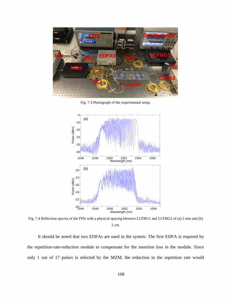
108
MLL
MZM
EDFA2
FPI
OC1Coupler
LCFBG3
PD
OscilloscopeAWG
OC2EDFA1
Fig. 7.3 Photograph of the experimental setup.
1546 1548 1550 1552 1554 1556-25
-22
-19
-16
-13
-10
Wavelength (nm)
Pow
er
(dB
m)
1546 1548 1550 1552 1554 1556Wavelength (nm)
-30
-25
-20
-15
-10
-5
Pow
er
(dB
m)
(a)
(b)
Fig. 7.4 Reflection spectra of the FPIs with a physical spacing between LCFBG1 and LCFBG2 of (a) 2 mm and (b)
2 cm.
It should be noted that two EDFAs are used in the system. The first EDFA is required by
the repetition-rate-reduction module to compensate for the insertion loss in the module. Since
only 1 out of 17 pulses is selected by the MZM, the reduction in the repetition rate would

109
introduce 12.3 dB insertion loss. If the insertion loss of the MZM of 5 dB is included, the total
insertion loss is 17.3 dB. If the pulse train generated by the MLL has a longer repetition period,
the first EDFA and the MZM will not be needed, and the system will be simplified. The insertion
loss of the FPI in the dispersion loop is 7.5 dB. The second EDFA is also required to compensate
for the round trip loss, to allow the pulse to recirculate for more round trips in the dispersive loop.
7.3 Experimental Results
The LCMW generated at the PD is monitored by an oscilloscope (Agilent DSO-X 93204A).
First, we use the FPI with a separation of d = 2 mm as the optical spectral shaper. Fig. 7.5 shows
two LCMWs after the pulse recirculates for three and five round trips in the loop. The LCMWs
have decreasing periods, indicating a frequency up-chirp. Compared with a single-time use of
LCFBG3 that would generate an LCMW with a duration of less than 10 ns, extended temporal
durations of around 25 and 42 ns are obtained for the two LCMWs. It should be noted that the
waveforms should have temporal durations of 30 and 50 ns calculated theoretically based on (8).
The differences in the temporal durations are due to the errors in the fabrication of the LCFBGs,
which would cause a reflection band mismatch between the LCFBGs. The amplitude ripples
shown in the LCMW spectra are due to the ripples in the spectrum of an MLL pulse, the non-flat
gain spectra of the EDFAs, and the ripples in the reflection spectra of the LCFBGs. The ripples
can be mitigated by adding an optical gain-flattening filter in the dispersive loop.
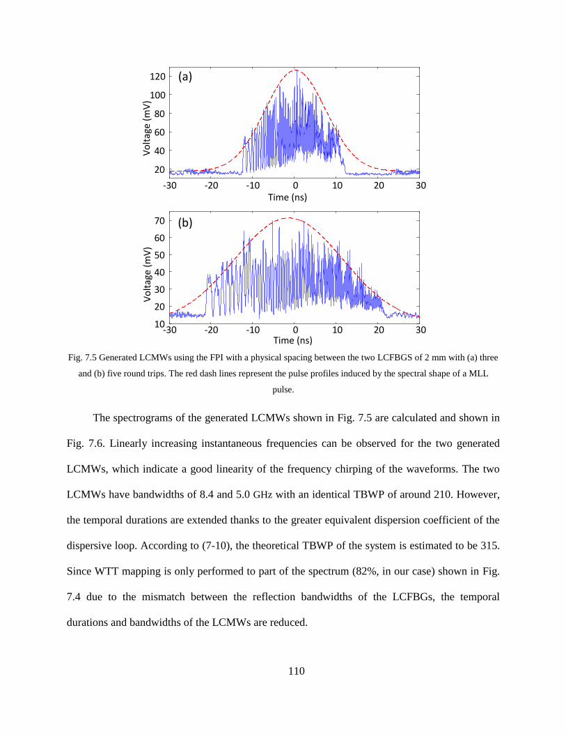
110
-30 -20 -10 0 10 20 3010
20
30
40
50
60
70
Time (ns)
Vo
ltag
e (m
V)
(b)
-30 -20 -10 0 10 20 30
20
40
60
80
100
120
Time (ns)
Vo
ltag
e (m
V)
(a)
Fig. 7.5 Generated LCMWs using the FPI with a physical spacing between the two LCFBGS of 2 mm with (a) three
and (b) five round trips. The red dash lines represent the pulse profiles induced by the spectral shape of a MLL
pulse.
The spectrograms of the generated LCMWs shown in Fig. 7.5 are calculated and shown in
Fig. 7.6. Linearly increasing instantaneous frequencies can be observed for the two generated
LCMWs, which indicate a good linearity of the frequency chirping of the waveforms. The two
LCMWs have bandwidths of 8.4 and 5.0 GHz with an identical TBWP of around 210. However,
the temporal durations are extended thanks to the greater equivalent dispersion coefficient of the
dispersive loop. According to (7-10), the theoretical TBWP of the system is estimated to be 315.
Since WTT mapping is only performed to part of the spectrum (82%, in our case) shown in Fig.
7.4 due to the mismatch between the reflection bandwidths of the LCFBGs, the temporal
durations and bandwidths of the LCMWs are reduced.

111
(a)
0 2 4 6 8 10 12
-30
-20
-
10
0
10
20
30
Tim
e (
ns)
Frequency (GHz)
(a)
0 2 4 6 8 10 12
-30
-20
-
10
0
10
20
30
Tim
e (
ns)
Frequency (GHz)
(b)(b)
0
0.4
0.7
0.9
0.3
0.2
0.1
0.5
0.6
0.8
1
Fig. 7.6 Spectrograms of the LCMWs for (a) three and (b) five round trips. The color scale represents the
normalized amplitude of the spectrogram.
In a microwave receiver, an LCMW is compressed by a matched filter to improve the
range resolution. The calculated correlation results between an LCMW and its reference are
presented in Fig. 7.7(a) and (b). The widths of the correlation peaks are 100 ps and 160 ps for the
two LCMWs after three and five round trips, which correspond to two suppression ratios of 250
and 262, respectively.
No
rma
lize
d A
mp
litu
de
-4 -2 0 2 40
0.2
0.4
0.6
0.8
1
Time (ns)-4 -2 0 2 4
0
0.2
0.4
0.6
0.8
1
Time (ns)
No
rma
lize
d A
mp
litu
de(a) (b)
Fig. 7.7 Calculated autocorrelation between the LCMWs and their references. For the FPI with a spacing of (a) 2
mm, and (b) 2 cm.

112
To generate an LCMW at a different frequency band, a second FPI with a physical
separation of d = 2 cm is then employed as the optical spectral shaper. The LCMW for five
round trips are shown in Fig. 7.8(a). A 45-ns long LCMW is achieved. The minimum frequency
is 1.5 GHz, instead of around DC for the LCMW shown in Fig. 7.5. However, strong attenuation
can be observed for the high frequency components due to a lower responsivity of the PD at a
higher frequency band. The spectrogram in Fig. 7.8(b) indicates a TBWP of only 180, which is
also caused by the lower responsivity of the PD at the higher frequency band. The calculated
autocorrelation of the LCMW shows a width of the correlation peak of 358 ps. A compression
ratio of 125 is achieved for the 45-ns long LCMW. It should be noted that amplitude ripples in
the spectra of the LCMWs shown in Fig. 7.5 and Fig. 7.8 are observed. The ripples are caused
due to the lasing in the dispersive loop since the gains at certain wavelengths are near the lasing
threshold. To reduce the ripples, in the dispersive loop, a gain-flattening filter may be used to
flatten the gain spectrum of the EDFA, so that the lasing can be suppressed.
-40 -30 -20 -10 0 10 20 30 40
10
20
30
40
50
60
Time (ns)
Volta
ge
(m
V)
(a)

113
0 2 4 6 8 10-30
-20
-10
0
10
20
30
Tim
e (
ns)
Frequency (GHz)
(b)
0
0.4
0.7
0.9
0.3
0.2
0.1
0.5
0.6
0.8
1
Fig. 7.8 (a) Generated LCMW using the FPI with a spacing of 2 cm after the optical pulse recirculates for five round
trips and (b) the corresponding spectrogram. The color scale represents the normalized amplitude of the
spectrogram. The red dash line in (a) represents the pulse profile induced by the spectral shape of a MLL pulse.
The stability of the proposed LCMW generator is also studied. We first investigate the
short term stability. To do so, two LCMWs that are separated in time by 60 cycles (45 s) are
sampled and compared. The LCMWs have very similar shapes, including the amplitude ripples
and the phase responses, indicating good stability and repeatability of the operation of the system.
The cross-correlation between the two LCMWs is also calculated which is identical to the auto-
correlation of one of the LCMWs. This again demonstrates a stable and repeatable operation of
the system. The long term stability is strongly affected by the ambient temperature change, as the
FPI is temperature sensitive. By using a temperature control unit, the long term stability can be
improved.

114
7.4 Conclusion
An approach to the generation of an LCMW with an extended temporal duration
implemented by an FPI for spectral shaping and a dispersive loop for wavelength-to-time
mapping was proposed and experimentally demonstrated. Long temporal duration for the
generated LCMW was enabled by multi-time use of an LCFBG in a dispersive loop to perform
WTT mapping. Two LCMWs with two temporal widths of 25 and 42 ns were generated at two
different frequency bands. A further increase in the temporal durations of the LCMWs is
possible by allowing the optical pulse recirculate for more round trips in the loop. The TBWPs of
the two LCMWs were both 210 and the extension of the temporal duration of an LCMW will not
increase the TBWP for a given FPI. To increase the TBWP, an FPI with two LCFBGs having
larger dispersion coefficients may be used. For example, if two LCFBGs with two opposite
dispersion coefficients of ±3188 ps2 are used to form the FPI and a PD with a bandwidth of over
100 GHz is used to perform photodetection [75], an LCMW with a TBWP as large as 4200 can
be generated.

115
CHAPTER 8 PHOTONIC TRUE-TIME DELAY
BEAMFORMING
A beamforming network is required to produce progressive phase or time delays for a PAA,
which can be implemented using phase shifters or true-time delay lines. In the past few years,
numerous photonic true-time delay beamforming networks have been demonstrated due to the
large operation bandwidth of a photonic system. However, all of the photonic true-time delay
beamforming networks requires a TLS array to achieve multi-channel tunable time delay, which
makes the system expensive and instable.
In this Chapter, we introduce a fiber-optic true-time delay beamforming network using a
switch-controlled recirculating wavelength-dependent dispersive loop incorporating an LCFBG
that only requires a laser array with fixed wavelengths. In the proposed system, a microwave
signal to be radiated to the free space is modulated on the multi-wavelength carrier from the laser
array, which is sent to a switch-controlled recirculating wavelength-dependent dispersive loop.
Since the optical signals with different wavelengths are reflected at different locations of the
LCFBG, different time delays are achieved. The tuning of the time delays are realized by
controlling the number of round trips the optical signals recirculate in the loop, which is done by
using a 2×2 optical switch to direct the optical signals back to the loop for additional time delays
or output of the loop. The proposed true-time delay beamforming network is experimentally
demonstrated. A four-channel true-time delay beamforming network using two different
recirculating dispersive loops with a true-time delay of 2.5 ns and 160 ps per round trip
incorporating two LCFBGs with different dispersion coefficients are demonstrated. The use of

116
the beamforming network to achieve arrayed beamforming that can cover -90° to 90° is
demonstrated.
8.1 Photonic True-Time Delay Based on a Dispersive Loop
The schematic diagram of the proposed true-time delay beamforming network is shown in
Fig. 8.1. The light waves from four laser diodes (LDs) with different wavelengths of 1 to 4 are
combined at a wavelength-division multiplexer (WDM1) and sent to an MZM, where a
microwave signal, generated by an electrical AWG, is modulated on the four wavelengths. The
modulated optical signals at the output of the MZM is then launched into a switch-controlled
wavelength-dependent optical dispersive recirculating loop through a 2x2 optical switch. An
LCFBG is incorporated in the loop via an OC to provide a wavelength-dependent time delay. An
EDFA1 is also incorporated in the loop to compensate for the loss in the loop so that an optical
signal can recirculate in the loop for multiple round trips. A programmable optical filter (OF)
with four passbands centered at 1 to 4 is also employed to suppress the ASE noise from the
EDFA. The number of round trips is controlled by the 2x2 optical switch. At the output of the
loop, a second EDFA (EDFA2) is used to further amplify the optical signal and a second WDM
(WDM2) is used to demultiplex the time-delayed optical signals in the four channels, which are
converted to four time delayed microwave signals at the PDs.
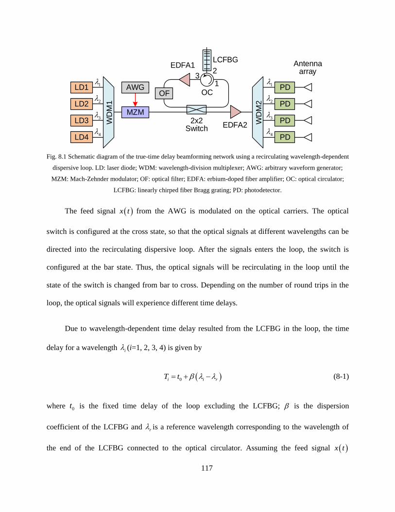
117
LD1
LD2
LD3
LD4
MZM
PD
PD
PD
PD
AWG
WD
M1
WD
M2
2x2Switch
EDFA1LCFBG
1
23
OC
Antennaarray
1
2
3
4
1
2
3
4
OF
EDFA2
Fig. 8.1 Schematic diagram of the true-time delay beamforming network using a recirculating wavelength-dependent
dispersive loop. LD: laser diode; WDM: wavelength-division multiplexer; AWG: arbitrary waveform generator;
MZM: Mach-Zehnder modulator; OF: optical filter; EDFA: erbium-doped fiber amplifier; OC: optical circulator;
LCFBG: linearly chirped fiber Bragg grating; PD: photodetector.
The feed signal x t from the AWG is modulated on the optical carriers. The optical
switch is configured at the cross state, so that the optical signals at different wavelengths can be
directed into the recirculating dispersive loop. After the signals enters the loop, the switch is
configured at the bar state. Thus, the optical signals will be recirculating in the loop until the
state of the switch is changed from bar to cross. Depending on the number of round trips in the
loop, the optical signals will experience different time delays.
Due to wavelength-dependent time delay resulted from the LCFBG in the loop, the time
delay for a wavelength i (i=1, 2, 3, 4) is given by
0i i rT t (8-1)
where 0t is the fixed time delay of the loop excluding the LCFBG; is the dispersion
coefficient of the LCFBG and r is a reference wavelength corresponding to the wavelength of
the end of the LCFBG connected to the optical circulator. Assuming the feed signal x t
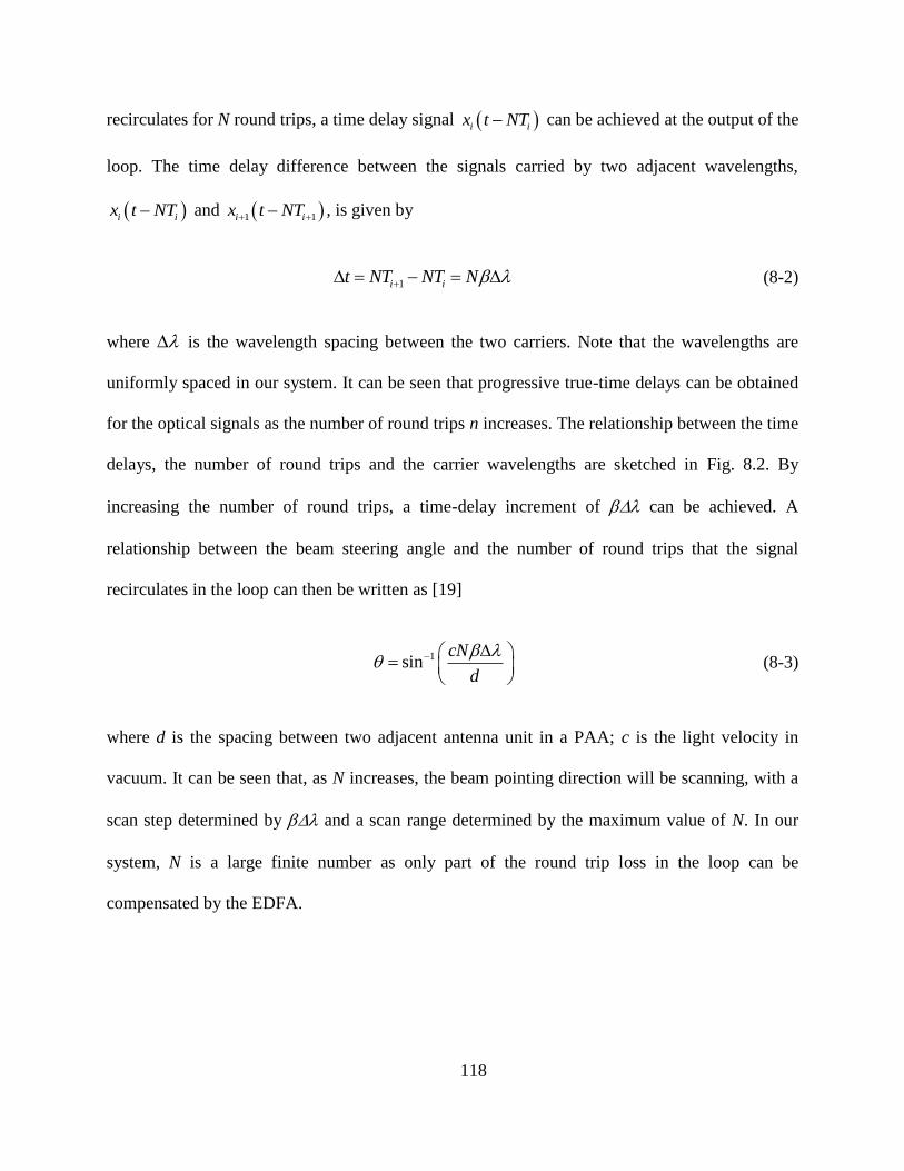
118
recirculates for N round trips, a time delay signal i ix t NT can be achieved at the output of the
loop. The time delay difference between the signals carried by two adjacent wavelengths,
i ix t NT and 1 1i ix t NT , is given by
1i it NT NT N (8-2)
where is the wavelength spacing between the two carriers. Note that the wavelengths are
uniformly spaced in our system. It can be seen that progressive true-time delays can be obtained
for the optical signals as the number of round trips n increases. The relationship between the time
delays, the number of round trips and the carrier wavelengths are sketched in Fig. 8.2. By
increasing the number of round trips, a time-delay increment of can be achieved. A
relationship between the beam steering angle and the number of round trips that the signal
recirculates in the loop can then be written as [19]
1sincN
d
(8-3)
where d is the spacing between two adjacent antenna unit in a PAA; c is the light velocity in
vacuum. It can be seen that, as N increases, the beam pointing direction will be scanning, with a
scan step determined by and a scan range determined by the maximum value of N. In our
system, N is a large finite number as only part of the round trip loss in the loop can be
compensated by the EDFA.
119
N=0
N=1
N=2
N=3
1234
2t
0t
t
3t
Relative time delay to Channel 1
Fig. 8.2 The time delay of the signal in each channel relative to channel 1 as the number of round trips N increases.
In microwave sensing applications, the temporal duration and the bandwidth of the feed
signal determine its spatial resolution and measurement range, and therefore are of great
importance [122]. In our system, it is required that the duration of the original microwave signal
should be smaller than the round trip time of the loop, so that the signal will not overlap with
itself when recirculates in the loop, i.e., the duration of the original microwave signal 0t .
Thanks to the small loss of optical fibers, t0 can be easily increased by using a long optical fiber
in the loop. Note that the loop length cannot be chosen arbitrarily long, since a longer dispersive
loop will slow down the beam steering speed. In addition to radial resolution, the angular
resolution of a radar is determined by the beam steering step, which can be calculated from (8-3)
for our system.
The bandwidth limit, on the other hand, is mostly determined by the opto-electronic
devices used in the system, such as the MZM and the PD. However, the dispersion-induced
power penalty [19] should also be considered as it may get significant due to the large equivalent

120
dispersion of a recirculating loop including an LCFBG, which is deduced to be N in Chapter 6.
To avoid the first zero-response point in the power distribution function of a system suffering
from dispersion-induce power penalty, it is required that the microwave signal frequency [19]
22 i
cf
N (8-4)
It should be noted that the dispersion-induced power penalty can be completely eliminated
by employing single-sideband with carrier (SSB+C) modulation [19], which is an effective way
to overcome the bandwidth limitation imposed by (8-4).
8.2 Experimental Implementation
Fig. 8.3 shows a photograph of the experimental setup, which is based on the schematic
diagram in Fig. 8.1. First, the experiment is carried out to have a large true-time delay step, i.e.,
is chosen to be large. The central wavelengths of the four LDs (Agilent N7714A) are set to
be 1548.9, 1549.9, 1550.9 and 1551.9 nm, which have a uniform wavelength spacing of 1 nm.
The OF is then programmed to have four 10-GHz-wide passbands at the same wavelengths. The
optical spectrum when the output of the four LDs are combined with the WDM presented in Fig.
8.4. Since the output power of the LDs are independently tunable, a flat optical comb is
generated. The LCFBG is fabricated to have a dispersion coefficient of 2500 ps/nm within its 4-
nm reflection band centered at 1550.5 nm (Fig. 8.5). It can be calculated that 2.5 ns , i.e.,
a true-time delay of 2.5 ns can be achieved between two adjacent channels when the signal
recirculates in the loop for one round trip. The AWG (Tektronix 7102), which has a sampling
rate of 10 Gb/s, is configured to generate the feed microwave signal. A 2x2 coupler is used

121
instead of the 2x2 switch to simplify the experiment and to study the round-trip-by-round-trip
behavior of the system. Although the coupler cannot actively control the number of round trips
that the optical signal recirculates in the loop, part of the optical signal will be coupled out of the
loop after each round trip, generating a stepped increasing true-time delay that corresponds to a
scanning steering beam angle for a PAA. Additionally, the extra 3-dB loss induced by the
coupler can be compensated by the EDFA in the loop. The time-delayed signals are detected by
four PDs with bandwidths of over 20 GHz and sampled by a 4-channel oscilloscope (Agilent
93204A).
LD 1-4 AWG
EDFA
MZM
OF
Oscilloscope
LCFBG
PDs
EDFA
WDM
WDM2x2Coupler
OC
Fig. 8.3 The photograph of the experimental setup.
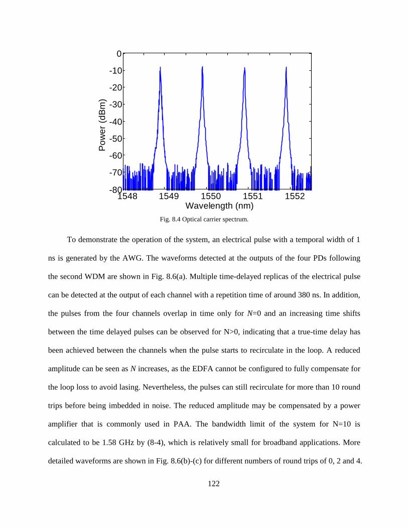
122
1548 1549 1550 1551 1552-80
-70
-60
-50
-40
-30
-20
-10
0
Wavelength (nm)
Po
we
r (d
Bm
)
Fig. 8.4 Optical carrier spectrum.
To demonstrate the operation of the system, an electrical pulse with a temporal width of 1
ns is generated by the AWG. The waveforms detected at the outputs of the four PDs following
the second WDM are shown in Fig. 8.6(a). Multiple time-delayed replicas of the electrical pulse
can be detected at the output of each channel with a repetition time of around 380 ns. In addition,
the pulses from the four channels overlap in time only for N=0 and an increasing time shifts
between the time delayed pulses can be observed for N>0, indicating that a true-time delay has
been achieved between the channels when the pulse starts to recirculate in the loop. A reduced
amplitude can be seen as N increases, as the EDFA cannot be configured to fully compensate for
the loop loss to avoid lasing. Nevertheless, the pulses can still recirculate for more than 10 round
trips before being imbedded in noise. The reduced amplitude may be compensated by a power
amplifier that is commonly used in PAA. The bandwidth limit of the system for N=10 is
calculated to be 1.58 GHz by (8-4), which is relatively small for broadband applications. More
detailed waveforms are shown in Fig. 8.6(b)-(c) for different numbers of round trips of 0, 2 and 4.

123
The time spacing between two pulses from two adjacent channels are measured to be 5.0 and
10.0 ns for N=2 and N=4, respectively, which are in perfect agreement with the theoretical values
of 2.5 ns per round trip. Due to the relatively large true-time delay, the system can be used for
PAAs with large antenna spacing and with a low operation frequency. Fig. 8.7 shows the
radiation patterns of a four-element linear PAA, which has a uniform element spacing of 5 m and
uses the time delayed signal after different numbers of round trips to feed the antenna elements.
A steering angle of 8.6° can be observed when the feed signal recirculates for one additional
round trip in the loop, which is in good agreement with (8-3). In four round trips, the beam
pointing direction is steered for 36.8°. With a sufficiently large N (over 13), the steering range
can fully cover -90° to 90°.
1547 1548 1549 1550 1551 1552 1553 1554
Wavelength (nm)
Re
fle
ctiv
ity (
%)
0
20
40
60
80
100
Gro
up
Dela
y (n
s)
0
2
4
6
8
10
Fig. 8.5 Spectral response of the LCFBG.
8.3 Performance Evaluation
An LCMW with a large bandwidth and a long time duration is commonly used as a feed
signal [70]. To test the performance of the system for a signal with long duration, the AWG is

124
configured to generate an LCMW with a time duration of 300 ns and a chirp rate of 2 MHz/ns
starting from DC. Fig. 8.8(a) shows the detected signals. Again, the signal carried by each
wavelength has a repetition time of 380 ns. The zoomed-in view of the signals after light
recirculateing for 0, 2 and 4 round trips are shown in Fig. 8.8(b)-(c). An increasing true-time
delay can be observed, which again agrees with the theoretical values. Since the duration of the
LCMW is shorter than the repetition time, the time delayed LCMWs do not overlap in time.
High signal-to-noise ratio is achieved even when the signal recirculates for more than six round
trips in the loop.
0 1 2 30
0.5
1
1.5
2
Time (s)
Vo
lta
ge
(m
V)
20 30 40 50 600
0.5
1
1.5
2
Time (ns)
Vo
lta
ge
(m
V)
790 800 810 820 830
0
0.2
0.4
0.6
0.8
1
Time (ns)
Vo
lta
ge
(m
V)
1560 1570 1580 1590 1600
0
0.1
0.2
0.3
0.4
0.5
0.6
Time (ns)
Vo
lta
ge
(m
V)
(a) (b)
(c) (d)
1234
N=0
N=1
N=2
N=3
N=4
N=5N=6
Fig. 8.6 Measured signals at the outputs of the four PDs when an electrical pulse is applied to the MZM. (a) The
generated time delayed replicas and the zoom-in view of the signals for (b) N=0, (c) N=2 and (d) N=4.

125
0.2
0.4
0.6
0.8
1
-30
150
-60
120
-90
90
-120
60
-150
30
180 0
0.2
0.4
0.6
0.8
1
-30
150
-60
120
-90
90
-120
60
-150
30
180 0
0.2
0.4
0.6
0.8
1
-30
150
-60
120
-90
90
-120
60
-150
30
180 0
0.2
0.4
0.6
0.8
1
-30
150
-60
120
-90
90
-120
60
-150
30
180 0
(a) (b)
(c) (d)
Fig. 8.7 Simulated radiation pattern of a four-element linear PAA with an element spacing of 5 m. The feed signals
to the antenna elements experience time delay of 2.5 ns per round trip in our true-time delay system. The PAA
initially points at 0°. (a)-(d) correspond to the radiation pattern when the feed signal recirculates for 0, 1, 2, and 4
round trips.

126
0 1 2 30
1
2
3
5
Time (s)
Vo
lta
ge
(m
V)
0 100 200 300 400
0
1
2
3
4
5
Time (ns)
Vo
lta
ge
(m
V)
800 900 1000 11000
0.5
1
1.5
2
2.5
3
Time (ns)
Vo
lta
ge
(m
V)
1500 1600 1700 1800 19000
0.5
1
1.5
2
Time (ns)
Vo
lta
ge
(m
V)
4
(a) (b)
(c) (d)
1234
N=0
N=1
N=2
N=3N=4
N=5
N=6
Fig. 8.8 Measured signals at the outputs of the four PDs when an LCMW is applied to the MZM. (a) The generated
time delayed replicas and the zoom-in view of the signals for (b) N=0, (c) N=2 and (d) N=4.
For a given beam steering angle, different amount of time delays are required for PAAs
with different antenna unit spacing. In our system, the true-time delay per round trip can be
easily changed by using LCFBGs with different dispersion coefficients or TLSs with different
wavelength spacing, according to (8-2). Here, an LCFBG with a dispersion coefficient of 200
ps/nm is employed, and the wavelength spacing between the TLSs are set to be 0.8 nm. A true-
time delay of 160 ps per round trip should be expected. Fig. 8.9 shows the measured time
delayed signals when a 1-ns electrical pulse is modulated to the multi-wavelength carrier. The
measured true-time delay is 159.2 ps per round trip. Fig. 8.10 shows the radiation pattern of a
four-element linear PAA when the time delayed signals are used as the inputs for the antenna
elements. Note that in this simulation, an initial time delay was applied so that the beam is

127
pointing at -28.5°. As the feed signal recirculate in the loop for 0, 1, 2 and 4 round trips, the
beam is steered to -13.9°, 0° and 28.5°. The PAA can cover a steering range from-90° to 90° if
the dispersive loop allows the optical signal to recirculate for over nine round trips. Assume the
signal recirculates in the loop for less than 10 round trips, the bandwidth limit of the system can
be calculated to be 5.59 GHz according to (8-4), which is significantly improved compared to the
case when a LCFBG with a dispersion coefficient of 2500 ps/nm is used. It can be seen that, in
order to get broadband true-time delay system with a large time delay, the best solution is to use
a LCFBG with small dispersion and TLSs with large wavelength spacing.
0 1 2 3
0
0.5
1
1.5
2
2.5
3
Time (s)
Vo
lta
ge
(m
V)
-4 -2 0 2 4
0
0.5
1
1.5
2
2.5
3
Time (ns)
Vo
lta
ge
(m
V)
767 769 771 773 775 777
0
0.5
1
1.5
Time (ns)
Vo
lta
ge
(m
V)
1539 1541 1543 1545 1547 1549
0
0.2
0.4
0.6
0.8
Time (ns)
Vo
lta
ge
(m
V)
(a) (b)
(c) (d)
1234
N=0
N=1
N=2
N=3
N=4
N=5N=6
Fig. 8.9 Measured signals at the outputs of the four PDs with a small true-time delay step of 160 ps, and with an
electrical pulse as the feed microwave signal. (a) The generated time delayed replicas and the zoom-in view of the
signals for (b) N=0, (c) N=2 and (d) N=4.

128
0.2
0.4
0.6
0.8
1
-30
150
-60
120
-90
90
-120
60
-150
30
180 0
0.2
0.4
0.6
0.8
1
-30
150
-60
120
-90
90
-120
60
-150
30
180 0
0.2
0.4
0.6
0.8
1
-30
150
-60
120
-90
90
-120
60
-150
30
180 0
0.2
0.4
0.6
0.8
1
-30
150
-60
120
-90
90
-120
60
-150
30
180 0
(a) (b)
(c) (d)
Fig. 8.10 Simulated radiation pattern of a four-element linear PAA with an element spacing of 20 cm. The feed
signals to the antenna elements experience time delay of 159.2 ps per round trip in our true-time delay system. The
PAA initially points at -28.5°. (a)-(d) correspond to the radiation pattern when the feed signal recirculates for 0, 1, 2,
and 4 round trips.
8.4 Discussion and Conclusion
The proposed beamforming system can be used to achieve tunable time delays for a pulsed
microwave signal. The pulse duration cannot be longer than the round trip time of the dispersive
loop to avoid overlap of two consecutive pulses. For a microwave signal with longer temporal
duration, the loop length should be longer. A longer dispersive loop will lead to a slower beam
steering speed since the steering speed is limited by the overall round trip time. For our proposed
129
system, the total time for 10 round trips is 3.8 s, which is fast enough for most radar
applications [148].
Note that the system can generate true time delays for a PAA with non-uniform element
spacing, which can be simply done by using a laser array with non-uniform wavelength spacing.
It should also be noted that the concept demonstrated here using a recirculating dispersive loop
can be applied for many other applications where a large tunable time delay is needed. Such a
system is also adaptable to the ripples in the group delay response of the LCFBG used in the
dispersive loop. As light recirculate in the loop, the ripples in the group delay response of the
LCFBG will start to affect the amount for time delay more significantly. This effect can be
mitigate by slightly adjusting the lasing wavelengths of the LDs.
In conclusion, we have proposed and experimentally demonstrated a photonic true-time
delay beamforming network based on a switch-controlled wavelength-dependent recirculating
dispersive loop. The microwave signal, with a temporal duration less than the round trip time of
the dispersive loop, to be radiated to free space was modulated on the optical carriers of a laser
array with fixed wavelengths. When the microwave-modulated optical signals recirculate in the
dispersive loop, due to the wavelength-dependent time delays in the LCFBG, tunable progressive
time delays could be achieved, which would lead to the beam steering when the time-delayed
microwave signals are fed to a PAA. It is different from some previously reported techniques
where the time delay tuning was realized by tuning the wavelength spacing of a laser array or the
dispersion coefficient of an LCFBG, the system here is simpler since a laser array with fixed
wavelengths is needed and the progressive time delays are generated and tuned by controlling the
number of the round trips of the optical signals recirculating in the dispersive loop. The proposed

130
true-time delay system was experimentally evaluated. In the experiment, an optical coupler
instead of an optical switch was used to study the tunable time delay behavior of the system.
Two true-time delay beamforming networks using two dispersive loops incorporating two
different LCFBGs with dispersion coefficients of 2500 ps/nm and 200 ps/nm to achieve a time
delay difference of 2.5 ns and 160 ps per round trip were demonstrated. The key advantage of the
proposed approach is its simplicity for implementation since no TLS and tunable LCFBG are
needed.

131
CHAPTER 9 SUMMARY AND FUTURE WORK
9.1 Summary
The work in this thesis focused on the use of an LCFBG-based DDL for the processing of
broadband microwave signals.
1) A broadband and precise microwave time reversal system using an LCFBG-based DDL
was proposed and experimentally demonstrated. By using the DDL that has opposite dispersion
coefficient when reflecting light at two different ends, a wideband microwave waveform
modulated on an optical pulse can be temporally reversed after the optical pulse is reflected by
the LCFBG for three times thanks to the opposite dispersion coefficient of the LCFBG when the
optical pulse is reflected from the opposite end. The time reversal of three different microwave
waveforms with a bandwidth of 4 GHz and a time duration of about 10 ns was demonstrated.
2) A microwave photonic matched filter was implemented for simultaneous generating and
compressing an arbitrary microwave waveform. The proposed microwave photonic signal
processor was verified by two experiments, in which a 7-bit PCMW with a carrier frequency of
4.08 GHz, and an LCMW with a bandwidth of 7.7 GHz were generated and compressed.
Compression ratios of 20.6 and 9.3 were achieved for the two waveforms. The proposed
microwave photonic signal processor can find applications in radar systems to generate and
compress wideband and high speed microwave signals.
3) Based on the microwave time reversal using an LCFBG-based DDL, a temporal
convolution system for the calculation of real time convolution of two wideband microwave
132
signals was demonstrated, which was realized by three photonic subsystems to perform the time
reversal, signal multiplication, and integration. The proposed approach was experimentally
evaluated, in which the calculations of three temporal convolutions between two rectangular
waveforms, between an inverse sawtooth waveform and a rectangular waveform, and between an
arbitrary waveform and a short pulse were experimentally demonstrated.
4) A novel time-stretched sampling system with a large stretching factor has been
demonstrated by a repetitive use of an LCFBG in a recirculating dispersive loop. An equivalent
GDD as large as 12000 ps/nm with a large stretching factor of 36 was achieved, which is the
largest dispersion coefficient ever reported in an optical DDL.
5) An approach to the generation of an LCMW with an extended temporal duration
implemented by an FPI for spectral shaping and a dispersive loop for wavelength-to-time
mapping was proposed and experimentally demonstrated. Long temporal duration for the
generated LCMW was enabled by multi-time use of an LCFBG in a dispersive to perform WTT
mapping. Two LCMWs with two temporal widths of 25 and 42 ns were generated at two
different frequency bands.
6) A fiber-optic true-time delay beamforming network using a switch-controlled
recirculating wavelength-dependent dispersive loop incorporating an LCFBG was demonstrated.
The tuning of the time delays are realized by controlling the number of round trips the optical
signals recirculate in the loop, which is done by using a 2×2 optical switch to direct the optical
signals back to the loop for additional time delays or output of the loop. A four-channel true-time
delay beamforming network using two different recirculating dispersive loops with a true-time
delay of 2.5 ns and 160 ps per round trip incorporating two LCFBGs with different dispersion
133
coefficients are demonstrated. The use of the beamforming network to achieve arrayed
beamforming that can cover -90° to 90° is demonstrated.
The photonic systems we demonstrated in this thesis have achieved an operation
bandwidth from several GHz to up to the THz range, and hence can be used to overcome the
bandwidth bottleneck of the digital signal processing techniques that are widely adopted in
modern microwave communication and radar systems.
9.2 Future work
In this thesis, we have developed several photonic systems based on optical DDLs that can
satisfy the bandwidth requirement of most modern microwave communication and radar systems.
However, the performance of some of the systems needs to be further improved. For example,
incoherent optical broadband source were used as the optical carrier source for the matched filter.
The incoherent source introduces a large amount of noise at the photodetector, which would have
negative influence on the overall performance of the system. A possible solution is to use a
wideband coherent optical source, such as a laser array, to generate an optical comb. When an
optical comb is used as the optical carrier, much lower noise will be generated. The interference
signal caused by beating of the optical comb will be at high frequency determined by the spacing
between the comb lines and can be removed by a low pass filter.
Another required improvement is with the fiber recirculating loop, which has been used for
microwave true-time delay beam forming, time stretched sampling and large TBWP generation.
Due to the existence of a gain medium in the loop, lasing occurs when the gain is larger than the
round trip loss, which would generate strong interference signal at a photodetector. It is very

134
important to find a solution to mitigate this effect. In our future work, we will try to use an
actively controlled optical switch to allow a pulse to recirculate in the loop for a certain number
of round trips while suppressing the lasing at the same time.
Finally, the photonic systems shown in the work are based on fiber optics. In the past years,
the development of silicon photonics, group III-V integrated photonics, and the integrated
photonics based on silicon nitride platform has enabled the implementation of such systems on a
chip. Group III-V integrated photonics will be our first choice as it provides optical source and
gain for the systems we demonstrated. The optical gain is especially important when a long
waveguide is required for a large time delay. For silicon and silicon nitride platforms, the
implementation of such a system requires hybrid integration with the group III-V components as
only passive components can be fabricated with silicon or silicon nitride. The advantage of the
silicon and silicon nitride platforms is the low waveguide loss, which allows an on-chip time
delay as large as tens of nanoseconds. Our future work will be developing integrated microwave
photonic systems to function as delay lines for broadband microwave signals and for the
realization of various microwave signal processing functions.

135
REFERENCES
[1] I. Frigyes and A. Seeds, “Optically generated true-time delay in phased-array antennas,”
IEEE Trans. Microw. Theory Tech., vol. 43, no. 9, pp. 2378-2386, Sep. 1995.
[2] P. Tournois, “Acousto-optic programmable dispersive filter for adaptive compensation of
group delay time dispersion in laser systems,” Opt. Commun., vol. 140, no. 4-6, pp. 245-
249, Aug. 1997.
[3] K. Iwashita and N. Takachio, “Chromatic dispersion compensation in coherent optical
communications,” J. Lightw. Technol., vol. 8, no.3, pp. 367-375, Mar. 1990.
[4] D. B. Sarrazin, H. F. Jordan, and V. P. Heuring, “Fiber optic delay line memory,” Appl.
Opt., vol. 29, pp. 627-637, Feb. 1990.
[5] R. Weigel, D. P. Morgan, J. M. Owens, A. Ballato, K. M. Lakin, K.-Y. Hashimoto, et al.,
“Microwave acoustic materials, devices, and applications,” IEEE Trans. Microw. Theory
Tech., vol. 50, no. 3, pp. 738-749, Mar. 2002.
[6] F. Zheng and T. Kaiser, Digital Signal Processing for RFID: John Wiley & Sons, 2016.
[7] C. Ruppel, C. Kappacher, L. Reindl, and G. Visintini, “Design and compensation of non-
equidistantly sampled SAW transducers,” in Proc. IEEE Ultrason. Symp, 1989, pp. 19-23.
[8] L. Reindl, U. Rosler, C. Ruppel, R. Obertreis, and R. Weigel, “Chirped SAW devices for
wireless passive sensors,” in Proc. IEEE Ultrason. Symp., Proceedings., 1997, pp. 343-
347.
[9] P. Santos, S. Rauwerdink, K. Biermann, B. Drescher, W. Seidel, M. Kaynak, et al.,
“Gigahertz monolithic delay lines for surface acoustic waves on Silicon,” in IOP
Conference Series: Materials Science and Engineering, 2012, p. 012009.
[10] S. Büyükköse, B. Vratzov, J. van der Veen, P. Santos, and W. van der Wiel, “Ultrahigh-
frequency surface acoustic wave generation for acoustic charge transport in silicon,” Appl.
Phys. Lett., vol. 102, p. 013112, Jan. 2013.
[11] G. Keiser, Optical fiber communications: Wiley Online Library, 2003.
[12] M. Laso, T. Lopetegi, M. Erro, D. Benito, M. Garde, M. Muriel, et al., “Chirped delay
lines in microstrip technology,” IEEE Microwav. Wireless Compon. Lett., vol. 11, no. 12,
pp. 486-488, Dec. 2001.
[13] J. Schwartz, Q. Zhuge, J. Azana, and D. Plant, “1-D uniform and chirped electromagnetic
bandgap structures in substrate integrated waveguides at 60 GHz,” Microw. Opt. Technol.
Lett., vol. 54, no. 3, pp. 735-737, Mar. 2012.
136
[14] F. Sangster, “Integrated MOS and bipolar analog delay lines using bucket-brigade
capacitor storage,” in IEEE International Solid-State Circuits Conference. Digest of
Technical Papers., 1970, pp. 74-75.
[15] J. Roderick, H. Krishnaswamy, K. Newton, and H. Hashemi, “Silicon-based ultra-
wideband beam-forming,” IEEE J. SOLID-ST. CIRC., vol. 41, no. 8, pp. 1726-1739, Aug.
2006.
[16] T.-S. Chu, J. Roderick, and H. Hashemi, “An integrated ultra-wideband timed array
receiver in 0.13 μm CMOS using a path-sharing true time delay architecture,” IEEE J.
SOLID-ST. CIRC., vol. 42, no. 12, pp. 2834-2850, Dec. 2007.
[17] J. Polivka, “An overview of microwave sensor technology,” High Freq. Electron., vol. 6,
pp. 32-42, 2007.
[18] M. I. Skolnik, RADAR Systems, McGraw-Hill, NY, 2001.
[19] J. P. Yao “Microwave photonics,” J. Lightw. Technol., vol. 27, no. 3, pp. 314-335, Feb.
2009.
[20] J. Capmany and D. Novak, “Microwave photonics combines two worlds,” Nat. Photonics,
vol. 1, no. 6, pp. 319–330, Apr. 2007.
[21] S. Yegnanarayanan, P. Trinh, F. Coppinger, and B. Jalali, “Compact silicon-based
integrated optic time delays,” IEEE Photon. Technol. Lett. vol. 9, no. 5, pp. 634-635,
May 1997.
[22] J. Cardenas, M. A. Foster, N. Sherwood-Droz, C. B. Poitras, H. L. Lira, B. Zhang, et al.,
“Wide-bandwidth continuously tunable optical delay line using silicon microring
resonators,” Opt. Express, vol. 18, no. 25, pp. 26525-26534, Dec. 2010.
[23] M. S. Rasras, C. K. Madsen, M. A. Cappuzzo, E. Chen, L. T. Gomez, E. J. Laskowski, et
al., “Integrated resonance-enhanced variable optical delay lines,” IEEE Photon. Technol.
Lett., vol. 17, no. 4, pp. 834-836, Apr. 2005.
[24] J. Mack, E. Burmeister, H. Poulsen, B. Stamenic, J. Bowers, and D. Blumenthal,
“Photonic integrated circuit switch matrix and waveguide delay lines for optical packet
synchronization,” in 2008 34th European Conference on Optical Communication, 2008,
pp. 1-2.
[25] T. Baba, “Slow light in photonic crystals,” Nat. Photon., vol. 2, no. 8, pp. 465-473, Aug.
2008.
[26] Y. Hamachi, S. Kubo, and T. Baba, “Slow light with low dispersion and nonlinear
enhancement in a lattice-shifted photonic crystal waveguide,” Opt. Lett., vol. 34, no. 7,
pp. 1072-1074, Apr. 2009.
137
[27] T. Erdogan, “Fiber grating spectra,” Lightwave Technology, Journal of, vol. 15, no. 8, pp.
1277-1294, Aug. 1997.
[28] W. Li, M. Li, and J. Yao, “A narrow-passband and frequency-tunable microwave
photonic filter based on phase-modulation to intensity-modulation conversion using a
phase-shifted fiber Bragg grating,” IEEE Trans. Microw. Theory Tech., vol. 60, no. 6, pp.
1287-1296, Jun. 2012.
[29] D. B. Hunter and R. A. Minasian, “Photonic signal processing of microwave signals
using an active-fiber Bragg-grating-pair structure,” IEEE Trans. Microw. Theory Tech.,
vol. 45, no. 8, pp. 1463-1466, Aug. 1997.
[30] R. Minasian, “Photonic signal processing of microwave signals,” IEEE Trans. Microw.
Theory Techn., vol. 54, no. 2, pp. 832-846, Feb. 2006.
[31] Y. Dai and J. Yao, “Nonuniformly spaced photonic microwave delay-line filters and
applications,” IEEE Trans. Microw. Theory Tech., vol. 58, no. 11, pp. 3279-3289, Nov.
2010.
[32] J. Mora, B. Ortega, A. Díez, J. L. Cruz, M. V. Andrés, J. Capmany, and D. Pastor,
“Photonic microwave tunable single-bandpass filter based on a Mach-Zehnder
interferometer,” J. Lightw. Technol., vol. 24, no. 7, pp. 2500-2509, Jul. 2006.
[33] X. Xue, X. Zheng, H. Zhang, and B. Zhou, “High-Q Single-Bandpass Photonic RF Filter
Overcoming Optical Third-Order Dispersion Based on Programmable Spectrum Shaping
of a Broadband Optical Source,” presented at the OFC, 2013.
[34] T. Jannson, “Real-time Fourier transformation in dispersive optical fibers,” Opt. Lett., vol.
8, no. 4, pp. 232-234, Apr. 1983.
[35] C. Wang, M. Li, and J. Yao, “Continuously tunable photonic microwave frequency
multiplication by use of an unbalanced temporal pulse shaping system,” IEEE Photon.
Technol. Lett., vol. 22, no. 17, pp. 1285-1287, Sep. 2010.
[36] H. Shahoei and J. Yao, “Continuously tunable microwave frequency multiplication by
optically pumping linearly chirped fiber Bragg gratings in an unbalanced temporal pulse
shaping system,” J. Lightw. Technol., vol. 30, no. 12, pp. 1954-1959, Jun. 2012.
[37] M. A. Muriel, J. Azaña, and A. Carballar, “Real-time Fourier transformer based on fiber
gratings,” Opt. Lett., vol. 24, no. 1, pp. 1-3, Jan. 1999.
[38] E. H. Zhou, H. Ruan, C. Yang, and B. Judkewitz, “Focusing on moving targets through
scattering samples,” Optica, vol. 1, no. 4, pp. 227-232, Oct. 2014.
[39] G. Lerosey, J. De Rosny, A. Tourin, A. Derode, G. Montaldo, and M. Fink, “Time
reversal of electromagnetic waves,” Phys. Rev. Lett., vol. 92, no. 19, pp. 193904-1-3,
May 2004.
138
[40] A. W. Rihaczek, “Principles of high-resolution radar,” Norwood, MA: Artech House,
1996.
[41] F. Coppinger, A. Bhushan, and B. Jalali, “Photonic time stretch and its application to
analog-to-digital conversion,” IEEE Trans. Microw. Theory Techn., vol. 47, no. 7, pp.
1309-1314, Jul. 1999
[42] F. Coppinger, A. Bhushan, and B. Jalali, “Time magnification of electrical signals using
chirped optical pulses,” Electronics Letters, vol. 34, no. 4, pp. 399-400, Feb. 1998.
[43] H. Chi, Y. Chen, Y. Mei, X. Jin, S. Zheng, and X. Zhang, “Microwave spectrum sensing
based on photonic time stretch and compressive sampling,” Opt. Lett., vol. 38, no. 2, pp.
136-138, Jan. 2013.
[44] Y. Chen, H. Chi, T. Jin, S. Zheng, X. Jin, and X. Zhang, “Sub-Nyquist sampled analog-
to-digital conversion based on photonic time stretch and compressive sensing with optical
random mixing,” J. Lightw. Technol., vol. 31, no. 21, pp. 3395-3401, Nov. 2013.
[45] B. W. Buckley, A. M. Madni, and B. Jalali, “Coherent time-stretch transformation for
real-time capture of wideband signals,” Opt. Express, vol. 21, no. 8, pp. 21618-21627,
Sep. 2013.
[46] Y. Han and B. Jalali, “Continuous-time time-stretched analog-to-digital converter array
implemented using virtual time gating,” IEEE Trans. Circuits Syst. Regul. Pap., vol. 52,
no. 8, pp. 1502-1507, Aug. 2005.
[47] M. H. Asghari and B. Jalali, “Anamorphic transformation and its application to time–
bandwidth compression,” Appl. Opt. vol. 52, no. 27, pp. 6735-6743, Sep. 2013.
[48] M. H. Asghari and B. Jalali, “Experimental demonstration of optical real-time data
compression,” Applied Physics Letters, vol. 104, p. 111101, Mar. 2014.
[49] J. Chou, O. Boyraz, D. Solli, and B. Jalali, “Femtosecond real-time single-shot digitizer,”
Appl. Phys. Lett., vol. 91, no. 16, pp. 161105-161105, Oct. 2007.
[50] B. M. Jung and J. P. Yao, “A two-dimensional optical true time-delay beamformer
consisting of a fiber Bragg grating prism and switch-based fiber-optic delay lines,” IEEE
Photon. Technol. Lett., vol. 21, no. 10, pp. 627-629, May 2009.
[51] S. Blais and J. P. Yao, “Photonic true-time delay beamforming based on superstructured
fiber Bragg gratings with linearly increasing equivalent chirps,” J. Lightw. Technol., vol.
27, no. 9, pp. 1147-1154, May 2009.
[52] Available: http://www.laserfocusworld.com/articles/print/volume-52/issue-
02/features/optics-fabrication-fiber-bragg-grating-fabrication-system-is-automated.html
139
[53] J. M. Moura and Y. Jin, “Detection by time reversal: single antenna,” IEEE Trans. Signal
Process., vol. 55, no. 1, pp. 187-201, Jan. 2007.
[54] G. Borzdov, “Localized electromagnetic and weak gravitational fields in the source-free
space,” Phys. Rev. E, vol. 63, pp. 036606, Feb. 2001.
[55] D. H. Chambers and J. G. Berryman, “Time-reversal analysis for scatterer
characterization,” Phys. Rev. Lett., vol. 92, no. 2, pp. 023902, Jan. 2004.
[56] W. Kuperman, W. S. Hodgkiss, H. C. Song, T. Akal, C. Ferla, and D. R. Jackson, “Phase
conjugation in the ocean: Experimental demonstration of an acoustic time-reversal
mirror,” J. Acoust. Soc. Am., vol. 103, no. 1, pp. 25-40, Jan. 1998.
[57] G. Lerosey, J. De Rosny, A. Tourin, A. Derode, G. Montaldo, and M. Fink, “Time
reversal of electromagnetic waves,” Phys. Rev. Lett., vol. 92, no. 19, pp. 193904-1-3,
May 2004.
[58] J. de Rosny, G. Lerosey, and M. Fink, “Theory of electromagnetic time-reversal mirrors,”
IEEE Trans. Antennas Propag., vol. 58, no. 10, pp. 3139-3149, Oct. 2010.
[59] P. Kosmas and C. M. Rappaport, “Time reversal with the FDTD method for microwave
breast cancer detection,” IEEE Trans. Microw. Theory Techn., vol. 53, no. 7, pp. 2317-
2323, Jul. 2005.
[60] P. Kosmas and C. M. Rappaport, “FDTD-based time reversal for microwave breast
cancer detection-localization in three dimensions,” IEEE Trans. Microw. Theory Techn.,
vol. 54, no. 4, pp. 1921-1927, Apr. 2006.
[61] B. Guo, L. Xu, and J. Li, “Time reversal based microwave hyperthermia treatment of
breast cancer,” in IEEE Thirty-Ninth Asilomar Conference on Signals, Systems and
Computers, pp. 290-293, Oct. 2005.
[62] H. D. Trefná, J. Vrba, and M. Persson, “Time-reversal focusing in microwave
hyperthermia for deep-seated tumors,” Phys. Med. Biol., vol. 55, no. 8, pp 2167-2185,
Mar. 2010.
[63] P. Kosmas, E. Zastrow, S. C. Hagness, and B. D. Van Veen, “A computational study of
time reversal techniques for ultra-wideband microwave hyperthermia treatment of breast
cancer,” in IEEE/SP 14th Workshop on Statistical Signal Processing, pp. 312-316, Aug.
2007.
[64] G. Lerosey, J. De Rosny, A. Tourin, and M. Fink, “Focusing beyond the diffraction limit
with far-field time reversal,” Science, vol. 315, no. 5815, pp. 1120-1122, Feb. 2007.
[65] A. Dezfooliyan and A. M. Weiner, “Experimental investigation of UWB impulse
response and time reversal technique up to 12 GHz: omnidirectional and directional
antennas,” IEEE Trans. Antennas Propag., vol. 60, no. 7, pp. 3407-3415, Jul. 2012.
140
[66] A. Derode, A. Tourin, and M. Fink, “Random multiple scattering of ultrasound. II. Is
time reversal a self-averaging process?” Phys. Rev. E, vol. 64, pp. 036606-1-13, Aug.
2001.
[67] H. Linget, L. Morvan, J.-L. Le Gouët, and A. Louchet-Chauvet, “Time reversal of
optically carried radiofrequency signals in the microsecond range,” Opt. Lett., vol. 38, no.
5, pp. 643-645, Mar. 2013.
[68] H. Linget, T. Chanelière, J.-L. Le Gouët, and A. Louchet-Chauvet, “Time reversal of
light by linear dispersive filtering near atomic resonance,” New J. Phys., vol. 15, pp.
063037-1-20, Jun. 2013.
[69] F. Coppinger, A. Bhushan, and B. Jalali, “Time reversal of broadband microwave signals,”
Electron. Lett., vol. 35, no. 15, pp. 1230-1232, Jul. 1999.
[70] J. Yao, “Photonic generation of microwave arbitrary waveforms,” Opt. Commun., vol.
284, no. 15, pp. 3723-3736, Jul. 2011.
[71] J. D. McKinney, D. Seo, D. E. Leaird, and A. M. Weiner, “ Photonically assisted
generation of arbitrary millimeter-wave and microwave electromagnetic waveforms via
direct space-to-time optical pulse shaping,” J. Lightw. Technol., vol. 21, no. 12, pp. 3020-
3028, Dec. 2003.
[72] S. T. Cundiff and A. M. Weiner, “Optical arbitrary waveform generation,” Nature
Photon., vol. 4, no. 11, pp. 760-766, Nov. 2010.
[73] A. Vega, D. E. Leaird, and A. M. Weiner, “High-speed direct space-to-time pulse
shaping with 1 ns reconfiguration,” Opt. Lett. vol. 35, no. 10, pp. 1554-1556, May 2010.
[74] A. Zeitouny, S. Stepanov, O. Levinson, and M. Horowitz, “Optical generation of linearly
chirped microwave pulses using fiber Bragg gratings,” IEEE Photon. Technol. Lett., vol.
17, no. 3, pp. 660-662, Mar. 2005.
[75] Y. Li, A. Rashidinejad, J.-M. Wun, D. E. Leaird, J.-W. Shi, and A. M. Weiner, “Photonic
generation of W-band arbitrary waveforms with high time-bandwidth products enabling
3.9 mm range resolution,” Optica, vol. 1, no. 6, pp. 446-454, Dec. 2014.
[76] Y. Li, A. Dezfooliyan, and A. M. Weiner, “Photonic synthesis of spread spectrum radio
frequency waveforms with arbitrarily long time apertures,” J. Lightw. Technol., vol. 32,
no. 20, pp. 3580-3587, Oct. 2014.
[77] J. Azaña, N. K. Berger, B. Levit, and B. Fischer, “Reconfigurable generation of high-
repetition-rate optical pulse sequences based on time-domain phase-only filtering,” Opt.
Lett., vol. 30, no. 23, pp. 3228-3230, Dec. 2005.

141
[78] Y. Dai and J. Yao, “Chirped microwave pulse generation using a photonic microwave
delay-line filter with a quadratic phase response,” IEEE Photon. Technol. Lett., vol. 21,
no. 9, pp. 569-571, May 2009.
[79] O. L. Coutinho, J. Zhang, and J. Yao, “Photonic generation of a linearly chirped
microwave waveform with a large time-bandwidth product based on self-heterodyne
technique,” in 2015 International Topical Meeting on Microwave Photonics (MWP), 26-
29 Oct. 2015, Paphos, Cypru.
[80] C. Wang and J. P. Yao, “Photonic generation of chirped microwave pulses using
superimposed chirped fiber Bragg gratings,” IEEE Photon. Technol. Lett., vol. 20, no. 11,
pp. 882-884, Jun. 2008.
[81] C. Wang and J. P. Yao, “Chirped microwave pulse generation based on optical spectral
shaping and wavelength-to-time mapping using a Sagnac-loop mirror incorporating a
chirped fiber Bragg grating,” J. Lightw. Technol., vol. 27, no. 16, pp.3336-3341, Aug.
2009.
[82] H. Shahoei and J. P. Yao, “Continuously tunable chirped microwave waveform
generation using a tilted fiber Bragg grating written in an erbium/ytterbium co-doped
fiber,” IEEE Photon. J., vol. 4, no. 3, pp. 765-771, Jun. 2012.
[83] M. H. Khan, H. Shen, Y. Xuan, L. Zhao, S. Xiao, D. E. Leaird, A. M. Weiner, and M. Qi,
“Ultrabroad-bandwidth arbitrary radiofrequency waveform generation with a silicon
photonic chip-based spectral shaper,” Nature Photon., vol. 4, no. 2, pp. 117-122, Feb.
2010.
[84] A. Rashidinejad and A. M. Weiner, “Photonic radio-frequency arbitrary waveform
generation with maximal time-bandwidth product capability,” J. Lightw. Technol., vol. 32,
no. 20, pp. 3383-3393, Oct. 2014.
[85] W. Li and J. P. Yao, “Generation of linearly chirped microwave waveform with an
increased time-bandwidth product based on a tunable optoelectronic oscillator and a
recirculating phase modulation loop,” J. Lightw. Technol., vol. 32, no. 20, pp. 3573-3579,
Oct. 2014.
[86] M. Li and J. P. Yao, “Photonic generation of a precisely pi phase shifted binary phase-
coded microwave signal,” IEEE Photon. Technol. Lett., vol. 24, no. 22, pp. 2001-2004,
Nov. 2012.
[87] W. Li, F. Kong, and J. P. Yao, “Arbitrary microwave waveform generation based on a
tunable optoelectronic oscillator,” J. Lightw. Technol., vol. 31, no. 23, pp. 3780-3786,
Dec. 2013.
[88] C. Wang and J. P. Yao, “Phase-coded millimeter-wave waveform generation using a
spatially discrete chirped fiber Bragg grating,” IEEE Photon. Technol. Lett., vol. 24, no.
17, pp. 1493-1495, Sep. 2012.
142
[89] A. M. Kawalec, “SAW dispersive delay lines in radar signal processing,” in Record of the
IEEE 1995 International Radar Conference, May 1995, pp. 732-736, Alexandria, VA.
[90] S. Gupta, D. L. Sounas, H. Van Nguyen, Q. Zhang, and C. Caloz, “CRLH–CRLH C-
Section Dispersive Delay Structures with Enhanced Group-Delay Swing for Higher
Analog Signal Processing Resolution,” IEEE Trans. Microw. Theory Tech., vol. 60, no.
12, pp. 3939-3949, Dec. 2012.
[91] Q. Zhang, S. Gupta, and C. Caloz, “Synthesis of narrowband reflection-type phasers with
arbitrary prescribed group delay,” IEEE Trans. Microw. Theory Tech., vol. 60, no. 8, pp.
2394-2402, Aug. 2012.
[92] C. Wang and J. P. Yao, “Chirped microwave pulse compression using a photonic
microwave filter with a nonlinear phase response,” IEEE Trans. Microw. Theory Tech.,
vol. 57, no. 2, pp. 496-504, Feb. 2009.
[93] Y. Dai and J. Yao, “Microwave correlator based on a nonuniformly spaced photonic
microwave delay-line filter,” IEEE Photon. Technol. Lett., vol. 21, no. 14, pp. 969-971,
Jul. 2009.
[94] M. Bolea, J. Mora, L. R. Chen, and J. Capmany, “Highly chirped reconfigurable
microwave photonic filter,” IEEE Photon. Technol. Lett., vol. 23, no. 17, pp. 1192-1194,
Sep. 2011.
[95] X. Xue, X. Zheng, H. Zhang, and B. Zhou, “Tunable chirped microwave photonic filter
employing a dispersive Mach–Zehnder structure,” Opt. Lett., vol. 36, no. 17, pp. 3518-
3520, Sep. 2011.
[96] A. E. Campbell-Washburn, H. Xue, R. J. Lederman, A. Z. Faranesh, and M. S. Hansen,
“Real-time distortion correction of spiral and echo planar images using the gradient
system impulse response function,” Magn. Reson. Med., 10.1002/mrm.25788, Jun. 2015.
[97] M. E. I. Martínez and F. E. H. Montero, “Detection of Periodic Signals in Noise Based on
Higher-Order Statistics Joined to Convolution Process and Spectral Analysis,” in
Progress in Pattern Recognition, Image Analysis, Computer Vision, and Applications,
Springer, 2013, pp. 488-495.
[98] J. Zhang, W. Liu, F. Kong, and J. P. Yao, “Microwave Hilbert transformer based on a
single passband microwave photonic filter for simultaneous channel selection and signal
processing,” J. Lightw. Technol., vol. 32, no. 17, pp. 2996-3001, Sep. 2014.
[99] J. Capmany, B. Ortega, and D. Pastor, “A tutorial on microwave photonic filters,” J.
Lightw. Technol., vol. 24, no. 1, pp. 201-229, Jan. 2006.
[100] J. Zhang and J. Yao, “Broadband and precise microwave time reversal using a single
linearly chirped fiber Bragg grating,” in Proc. Int. Topical Meeting on Microw. Photon.
and 9th Asia–Pacific Microw. Photon. Conf., Oct. 2014, pp. 57–60, paper TuD-2.

143
[101] J. Zhang and J. Yao, “Broadband and precise microwave time reversal using a single
linearly chirped fiber Bragg grating,” IEEE Trans. Microw. Theory Techn., vol. 63, no. 7,
pp. 2166-2172, Jul. 2015.
[102] R. Slavík, Y. Park, N. Ayotte, S. Doucet, T.-J. Ahn, S. LaRochelle, and J. Azaña,
“Photonic temporal integrator for all-optical computing,” Opt. Express, vol. 16, no. 22,
pp. 18202-18214, Oct. 2008.
[103] W. Liu, M. Li, R. S. Guzzon, E. J. Norberg, J. S. Parker, L. A. Coldren, and J. P. Yao,
“Photonic temporal integrator with an ultra-long integration time window based on an
InP-InGaAsP integrated ring resonator,” J. Lightw. Technol., vol. 32, no. 20, pp. 3654-
3659, Oct. 2014.
[104] M. Ferrera, Y. Park, L. Razzari, B. E. Little, S. T. Chu, R. Morandotti, D. Moss, and J.
Azaña, “On-chip CMOS-compatible all-optical integrator,” Nat. Comm., vol. 1, pp. 29,
Jun. 2010.
[105] N. Huang, M. Li, R. Ashrafi, L. Wang, X. Wang, J. Azaña, and N. Zhu, “Active Fabry-
Perot cavity for photonic temporal integrator with ultra-long operation time window,”
Opt. Express, vol. 22, no. 3, pp. 3105-3116, Feb. 2014.
[106] Y. Park and J. Azaña, “Ultrafast photonic intensity integrator,” Opt. Lett., vol. 34, no. 8,
pp.1156-1158, Apr. 2009.
[107] M. H. Asghari, Y. Park, and J. Azaña, “Photonic temporal integration of broadband
intensity waveforms over long operation time windows,” Opt. Lett., vol. 36, no. 18, pp.
3557-3559, Sep. 2011.
[108] A. Malacarne, R. Ashrafi, M. Li, S. LaRochelle, J. Yao, and J. Azaña, “Single-shot
photonic time-intensity integration based on a time-spectrum convolution system,” Opt.
Lett., vol. 37, no. 8, pp. 1355-1357, Apr. 2012.
[109] H. Jiang, L. Yan, J. Ye, W. Pan, B. Luo, and X. Zou, “Tunable Microwave Photonic
Temporal Signal Processor: Differentiator and Integrator,” IEEE Photon. Technol. Lett.,
vol. 25, no. 23, pp. 2358-2361, Dec. 2013.
[110] M. Li, L.-Y. Shao, J. Albert, and J. Yao, “Continuously tunable photonic fractional
temporal differentiator based on a tilted fiber Bragg grating,” IEEE Photon. Technol.
Lett., vol. 23, no. 4, pp. 251-253, Feb. 2011.
[111] H. Yu, W. Fang, X. Wu, X. Lin, L. Tong, W. Liu, A. Wang, and Y. R. Shen, “Single
nanowire optical correlator,” Nano Lett., vol. 14, no. 6, pp. 3487-3490, May 2014.
[112] P. W. Juodawlkis, J. J. Hargreaves, R. D. Younger, G. W. Titi, and J. C. Twichell,
“Optical down-sampling of wide-band microwave signals,” J. Lightw. Technol., vol. 21,
no. 12, pp. 3116, Dec. 2003.

144
[113] B. C. Pile and G. W. Taylor, “Performance of Subsampled Analog Optical Links,” J.
Lightw. Technol., vol. 30, no. 9, pp. 1299-1305, May 2012.
[114] A. Feldster, Y. P. Shapira, M. Horowitz, A. Rosenthal, S. Zach, and L. Singer, “Optical
under-sampling and reconstruction of several bandwidth-limited signals,” J. Lightw.
Technol., vol. 27, no. 8, pp. 1027-1033, Apr. 2009.
[115] M. B. Airola, S. R. O'Connor, M. L. Dennis, and T. R. Clark, “Experimental
demonstration of a photonic analog-to-digital converter architecture with pseudorandom
sampling,” IEEE Photon. Technol. Lett., vol. 20, no. 24, pp. 2171-2173, Dec. 2008.
[116] G. C. Valley, G. A. Sefler, and T. J. Shaw, “Compressive sensing of sparse radio
frequency signals using optical mixing,” Opt. Lett., vol. 37, no. 22, pp. 4675-4677, Nov.
2012.
[117] X. Dong, P. Shum, N. Ngo, C. Chan, J. Ng, and C. Zhao, “A largely tunable CFBG-based
dispersion compensator with fixed center wavelength,” Opt. Express, vol. 11, no. 22, pp.
2970-2974, Nov. 2003.
[118] J. D. Schwartz, J. Azaña, and D. V. Plant, “Experimental demonstration of real-time
spectrum analysis using dispersive microstrip,” IEEE Microwav. Wireless Compon. Lett.,
vol. 16, no.4, pp. 215-217, Apr. 2006.
[119] M. A. Laso, T. Lopetegi, M. J. Erro, D. Benito, M. J. Garde, M. A. Muriel, et al., “Real-
time spectrum analysis in microstrip technology,” IEEE Trans. Microw. Theory Tech.,
vol. 51, no. 3, pp. 705-717, Mar. 2003.
[120] B. Nikfal, S. Gupta, and C. Caloz, “Increased Group-Delay Slope Loop System for
Enhanced-Resolution Analog Signal Processing,” IEEE Trans. Microw. Theory Tech.,
vol. 59, no. 6, pp. 1622-1628, Jun. 2011.
[121] D. K. Barton, Radar System Analysis and Modeling, Artech House, 2004.
[122] A. W. Rihaczek, Principles of High-Resolution Radar, McGraw-Hill New York, 1969.
[123] R. Skaug and J. F. Hjelmstad, Spread Spectrum in Communication, London, U.K., 1985.
[124] M. Bertero, M. Miyakawa, P. Boccacci, F. Conte, K. Orikasa, and M. Furutani, “Image
restoration in chirp-pulse microwave CT (CP-MCT),” IEEE Trans. Biomed. Eng., vol. 47,
no. 5, pp. 690–699, May 2000.
[125] J. Levy, P. Burke, L. Cohen, and R. Cecchini, “VCO based chirp generation for broad
bandwidth compressive receiver applications (in EW),” IEEE MTT-S International
Microwave Symposium Digest, vol. 3, pp. 1113-1115, Jun. 1993.
145
[126] A. Stelzer, K. Ettinger, J. Hoftberger, J. Fenk, and R. Weigel, “Fast and accurate ramp
generation with a PLL-stabilized 24-GHz SiGe VCO for FMCW and FSCW applications,”
IEEE MTT-S International Microwave Symposium Digest, vol. 2, pp. 893-896, Jun. 2003.
[127] D. Gomez-Garcia, C. Leuschen, F. Rodriguez-Morales, J.-B. Yan, and P. Gogineni,
“Linear chirp generator based on direct digital synthesis and frequency multiplication for
airborne FMCW snow probing radar,” IEEE MTT-S International Microwave Symposium
Digest, pp. 1-4, Jun. 2014.
[128] I. S. Merrill, Introduction to radar systems, McGrow-Hill, 2001.
[129] M. Longbrake, “True time-delay beamsteering for radar,” in Aerospace and Electronics
Conference (NAECON), 2012 IEEE National, 2012, pp. 246-249.
[130] H. Shahoei and J. P. Yao, “Delay lines,” Wiley Encyclopedia of Electrical and
Electronics Engineering, 1–15, DOI: 10.1002/047134608X.W8234, Dec. 2014.
[131] J. Schwartz, Q. Zhuge, J. Azaña, and D. Plant, “1-D uniform and chirped electromagnetic
bandgap structures in substrate integrated waveguides at 60 GHz,” Microw. Opt. Technol.
Lett., vol. 54, no. 3, pp. 735-737, Mar. 2012.
[132] D. Dolfi, P. Joffre, J. Antoine, J.-P. Huignard, D. Philippet, and P. Granger,
“Experimental demonstration of a phased-array antenna optically controlled with phase
and time delays,” Appl. Opt., vol. 35, no. 26, pp. 5293-5300, Sep. 1996.
[133] Y. Liu, J. Yao, and J. Yang, “Wideband true-time-delay unit for phased array
beamforming using discrete-chirped fiber grating prism,” Opt. Commun., vol. 207, no. 1,
pp. 177-187, Jun. 2002.
[134] Y. Liu, J. Yang, and J. Yao, “Continuous true-time-delay beamforming for phased array
antenna using a tunable chirped fiber grating delay line,” IEEE Photon. Technol. Lett.,
vol. 14, no. 8, pp. 1172-1174, Aug. 2002.
[135] D.-H. Yang and W.-P. Lin, “Phased-array beam steering using optical true time delay
technique,” Opt. Commun., vol. 350, pp. 90-96, Sep. 2015.
[136] X. Ye, F. Zhang, and S. Pan, “Optical true time delay unit for multi-beamforming,” Opt.
Express, vol. 23, no. 8, pp. 10002-10008, Apr. 2015.
[137] Y. Minamoto and M. Matsuura, “True-time delay beamforming using semiconductor
optical amplifier and tunable dispersion medium,” in IEEE International Conference on
Network Infrastructure and Digital Content (IC-NIDC), 2014 4th 2014, pp. 164-167.
[138] S. Garcia and I. Gasulla, “Design of heterogeneous multicore fibers as sampled true-time
delay lines,” Opt. Lett., vol. 40, no. 4, pp. 621-624, Feb. 2015.

146
[139] S. Chin, L. Thévenaz, J. Sancho, S. Sales, J. Capmany, P. Berger, J. Bourderionnet and D.
Dolfi, “Broadband true time delay for microwave signal processing, using slow light
based on stimulated Brillouin scattering in optical fibers,” Opt. Express, vol. 18, no. 21.
pp. 22599-22613, Oct. 2010.
[140] J. Wang, P. Hou, H. Cai, J. Sun, S. Wang, L. Wang and F. Yang, “Continuous angle
steering of an optically-controlled phased array antenna based on differential true time
delay constituted by micro-optical components,” Opt. Express, vol. 23, no. 7, pp. 9432-
9439, Mar. 2015.
[141] L. Zhuang, M. Hoekman, C. Taddei, A. Leinse, R. G. Heideman, A. Hulzinga, et al.,
“On-chip microwave photonic beamformer circuits operating with phase modulation and
direct detection,” Opt. Express, vol. 22, no. 14, pp. 17079-17091, Jul. 2014.
[142] M. Burla, D. A. Marpaung, L. Zhuang, M. R. Khan, A. Leinse, W. Beeker, et al.,
“Multiwavelength-integrated optical beamformer based on wavelength division
multiplexing for 2-D phased array antennas,” J. Lightw. Technol.,vol. 32, no. 20, pp.
3509-3520, Oct. 2014.
[143] R. Bonjour, S. A. Gebrewold, D. Hillerkuss, C. Hafner, and J. Leuthold, “Continuously
tunable true-time delays with ultra-low settling time,” Opt. Express, vol. 23, no. 5, pp.
6952-6964, Feb. 2015.
[144] H. Chi and J. P. Yao, “Symmetrical waveform generation based on temporal pulse
shaping using an amplitude-only modulator,” IEEE Electron. Lett., vol. 43, no. 7, pp.
415-417, Mar. 2007.
[145] C. Wang, M. Li, and J. P. Yao, “Continuously tunable photonic microwave frequency
multiplication by use of an unbalanced temporal pulse shaping system,” IEEE Photon.
Technol. Lett., vol. 22, no. 17, pp. 1285-1287, Aug. 2010.
[146] M. Weeks, Digital Signal Processing Using MATLAB & Wavelets: Jones & Bartlett
Learning, 2010.
[147] G. P. Agrawal, Nonlinear Fiber Optics: Springer, 2000.
[148] A. Farina and P. Neri, “Multitarget interleaved tracking for phased-array radar,” IEE
Proc. F Comm., Radar Signal Process., vol. 127, no. 4, pp. 312-318, Aug. 1980.
147
Publications
Journal Papers:
[1] J. Zhang and J. P. Yao, “Broadband microwave signal processing based on photonic
dispersive delay line,” IEEE Trans. Microw. Theory Tech., accepted (Invited).
[2] J. Zhang and J. P. Yao, “A microwave photonic signal processor for arbitrary
microwave waveform generation and pulse compression,” IEEE/OSA J. Lightw.
Technol., vol. 34, no. 24, pp. 5610-5615, Dec. 2016.
[3] J. Zhang and J. P. Yao, “Photonic true-time delay beamforming using a switch-
controlled wavelength-dependent recirculating loop,” IEEE/OSA J. Lightw. Technol.,
vol. 34, no. 16, pp. 3923-3929, Aug. 2016.
[4] J. Zhang and J. P. Yao, “Photonic-assisted microwave temporal
convolution,” IEEE/OSA J. Lightw. Technol., vol. 34, no. 20, pp. 4652-4657, Oct.
2016.
[5] J. Zhang, O. L. Coutinho, and J. P. Yao, “Photonic generation of a linearly chirped
microwave waveform with extended temporal duration using a dispersive loop,”
IEEE Trans. Microw. Theory Tech., vol. 64, no. 6, pp. 1947-1953, Jun. 2016.
[6] J. Zhang and J. P. Yao, “Microwave photonic integrator based on a multichannel
fiber Bragg grating,” Opt. Lett., vol. 41, no. 2, pp. 273-276, Jan. 2016.

148
[7] J. Zhang and J. P. Yao, “Ultrafast three-dimensional serial time-encoded imaging
with high vertical resolution,” IEEE/OSA J. Lightw. Technol., vol. 33, no. 22, pp.
4622-4626, Nov. 2015.
[8] J. Zhang and J. Yao, “Broadband and precise microwave time reversal using a single
linearly chirped fiber Bragg grating,” IEEE Trans. Microw. Theory Tech., vol. 63, no.
7, pp. 2166-2172, Jul. 2015.
[9] J. Zhang, W. Liu, F. Kong, and J. P. Yao, “Microwave Hilbert transformer based on
a single passband microwave photonic filter for simultaneous channel selection and
signal processing,” IEEE/OSA J. Lightw. Technol., vol. 32, no. 17, pp. 2996-3001,
Sep. 2014.
[10] J. Zhang and J. P. Yao, “Time stretched sampling of a fast microwave waveform
based on the repetitive use of a linearly chirped fiber Bragg grating in a dispersive
loop,” Optica, vol. 1, no. 2, pp. 64-69, Aug. 2014.
[11] J. Zhang, L. Gao, and J. P. Yao, “Tunable optoelectronic oscillator incorporating a
single passband microwave photonic filter,” IEEE Photon. Technol. Lett., vol. 26, no.
4, pp. 326-329, Feb. 2014.
[12] O. Xu, J. Zhang, H. Deng, and J. P. Yao, “Dual-frequency optoelectronic oscillator
for temperature-insensitive interrogation of a FBG sensor,” IEEE Photon. Technol.
Lett., accepted.

149
[13] O. Xu, J. Zhang, and J. P. Yao, “High speed and high resolution interrogation of a
fiber Bragg grating sensor based on microwave photonic filtering and chirped
microwave pulse compression,” Opt. Lett., vol. 41, no. 21, pp. 4859-4862, Nov. 2016.
[14] Y. Wang, J. Zhang, and J. P. Yao, “An optoelectronic oscillator for high sensitivity
temperature sensing,” IEEE Photon. Technol. Lett., vol. 28, no. 13, pp 1458-1460, Jul.
2016.
[15] Y. Wang, J. Zhang, O. L. Coutinho, and J. P. Yao, “Interrogation of a linearly
chirped fiber Bragg grating sensor with a high resolution using a linearly chirped
optical waveform,” Opt. Lett., vol. 40. no. 21, pp. 4923-4926, Nov. 2015.
[16] R. Ashrafi, M. R. Dizaji, L. R. Cortés, J. Zhang, J. P. Yao, J. Azaña, and L. R. Chen,
“Time-delay to intensity mapping based on a second-order optical integrator:
application to optical arbitrary waveform generation,” Opt. Express, vol. 23, no. 12,
pp. 16209-16223, Jun. 2015.
[17] W. Liu, J. Zhang, M. Rioux, J. Viens, Y. Messaddeq, and J. P. Yao, “Frequency
tunable continuous THz wave generation in a periodically poled fiber,” IEEE Trans.
THz Sci. Technol., vol. 5, no. 3, pp. 470-477, May 2015.
[18] F. Kong, B. Romeira, J. Zhang, W. Li, and J. P. Yao, “A dual-wavelength fiber ring
laser incorporating an injection-coupled optoelectronic oscillator and its application
to transverse load sensing,” IEEE/OSA J. Lightw. Technol., vol. 32, no. 9, pp. 1784-
1793, May 2014.

150
[19] L. Gao, J. Zhang, X. Chen, and J. P. Yao, “Microwave photonic filter with two
independently tunable passbands using a phase modulator and an equivalent phase-
shifted fiber Bragg grating,” IEEE Trans. Microw. Theory Tech., vol. 62, no. 2, pp.
380-387, Feb. 2014.
Conference Papers:
[1] J. Zhang and J. P. Yao, “A photonic integrated microwave waveform generator for
linearly chirped microwave waveform generation,” MWP2016, Long Beach,
California, USA, Oct. 2016.
[2] J. Zhang, O. Coutinho, and J. P. Yao, “Photonic generation of a linearly chirped
microwave waveform with long temporal duration using a dispersive loop,” IMS
2015, TU3G-2, 17-22 May 2015, Phoenix, Arizona, USA.
[3] J. Zhang and J. P. Yao, “Broadband and precise microwave time reversal using a
single linearly chirped fiber Bragg grating,” MWP2014, Sapporo, Japan, 20-23 Oct.
2014. (Best student paper)
[4] J. Zhang, M. H. Asghari, B. Jalali, and J. P. Yao, “Time-bandwidth product
expansion of microwave waveforms using anamorphic stretch transform,” CLEO
2014, 8-13 June 2014, San Jose, USA, paper JTh2A.38.
[5] O. L. Coutinho, J. Zhang, and J. P. Yao, “Photonic generation of a linearly chirped
microwave waveform With a Large time-bandwidth product based on self-heterodyne
technique,” MWP2015, 26-29 Oct. 2015, Paphos, Cypru.
151
[6] W. Zhang, J. Zhang and J. P. Yao, “Largely chirped microwave waveform
generation using a silicon-based on-chip optical spectral shaper,” MWP2014,
Sapporo, Japan, 20-23 Oct. 2014.