photonic light-trapping versus lambertian limits in thin ... · angelo bozzola,∗ marco liscidini,...
TRANSCRIPT
Photonic light-trapping versusLambertian limits in thin film siliconsolar cells with 1D and 2D periodic
patterns
Angelo Bozzola,∗ Marco Liscidini, and Lucio Claudio AndreaniDipartimento di Fisica “Alessandro Volta”, Universita degli Studi di Pavia, via Bassi 6,
I-27100 Pavia, Italy∗[email protected]
Abstract: We theoretically investigate the light-trapping properties ofone- and two-dimensional periodic patterns etched on the front surface ofc-Si and a-Si thin film solar cells with a silver back reflector and an anti-reflection coating. For each active material and configuration, absorbanceA and short-circuit current density Jsc are calculated by means of rigorouscoupled wave analysis (RCWA), for different active materials thicknessesin the range of interest of thin film solar cells and in a wide range ofgeometrical parameters. The results are then compared with Lambertianlimits to light-trapping for the case of zero absorption and for the generalcase of finite absorption in the active material. With a proper optimization,patterns can give substantial absorption enhancement, especially for 2Dpatterns and for thinner cells. The effects of the photonic patterns onlight harvesting are investigated from the optical spectra of the optimizedconfigurations. We focus on the main physical effects of patterning, namelya reduction of reflection losses (better impedance matching conditions),diffraction of light in air or inside the cell, and coupling of incident radiationinto quasi-guided optical modes of the structure, which is characteristic ofphotonic light-trapping.
© 2012 Optical Society of America
OCIS codes: (040.5350) Photovoltaic; (050.5298) Photonic crystals.
References and links1. J. Nelson, The Physics of Solar Cells (Imperial College Press, London 2003).2. J. Poortmans and V. Arkhipov (editors), Thin Film Solar Cells (Wiley, Chichester, 2006).3. AM1.5 solar spectrum irradiance data: http://rredc.nrel.gov/solar/spectra/am1.5.4. E. D. Palik, Handbook of Optical Constants of Solids (Academic, Orlando 1985).5. D. T. Pierce, W. E Spicer, “Electronic structure of amorphous Si from photoemission and optical studies,” Phys.
Rev. B 5, 3017–3029 (1972).6. M. I. Alonso, M. Garriga, C. A. Durante Rincan, E. Hernandez, and M. Leon, “Optical functions of chalcopyrite
CuGaxIn1−xSe2 alloys,” Appl. Phys. A 74, 659–664 (2002).7. E. Yablonovitch, “Statistical ray optics,” J. Opt. Soc. Am. 72, 899–907 (1982).8. E. Yablonovitch and G. D. Cody, “Intensity enhancement in textured optical sheets for solar cells,” IEEE Trans.
Electron. Dev. 29, 300–305 (1982).9. M. A. Green, “Lambertian light trapping in textured solar cells and light-emitting diodes: analytical solutions,”
Progr. Photovolt: Res. Appl. 10, 235–241 (2002).10. K. R. Catchpole and A. Polman, “Design principles for particle plasmon enhanced solar cells,” Appl. Phys. Lett.
93, 191113 (2008).
#156735 - $15.00 USD Received 18 Oct 2011; revised 7 Dec 2011; accepted 8 Dec 2011; published 30 Jan 2012(C) 2012 OSA 12 March 2012 / Vol. 20, No. S2 / OPTICS EXPRESS A224
11. K. R. Catchpole and A. Polman, “Plasmonic solar cells,” Opt. Express 16, 21793–21800 (2008).12. H. A. Atwater and A. Polman, “Plasmonics for improved photovoltaic devices,” Nature Mat. 9, 205–213 (2010).13. J.N. Munday and H.A. Atwater, “Large integrated absorption enhancement in plasmonic solar cells by combining
metallic gratings and antireflection coatings,” Nano Lett. 11, 2195–2201 (2011).14. J. Krc, M. Zeman, O. Kluth, F. Smole, and M. Topic, “Effect of surface roughness of ZnO:Al films on light
scattering in hydrogenated amorphous silicon solar cells,” Thin Solid Films 426, 296–304 (2003).15. J. Krc, G. Cernivec, A. Campa, J. Malmstrom, M. Edoff, F. Smole, and M. Topic, “Optical and electrical modeling
of Cu(In,Ga)Se2 solar cells,” Optical and Quantum Electronics 38, 1115–1123 (2006).16. M. Peters, C. Battaglia, A. G. Aberle, B. Blasi, J. Luther, and S. Glunz, “3D optical simulation of scattering in
thin film silicon solar cells,” in Proceedings of the 26th European Photovoltaic Solar Energy Conference andExhibition, (Hamburg, September 5-9, 2011) paper 3AV.3.4.
17. M. Agrawal and M. Frei, “Rigorous optical modeling and optimization of thin-film photovoltaic cells with tex-tured transparent conductive oxides,” Prog. Photovolt: Res. Appl. DOI: 10.1002/pip.1158 (2011).
18. T. Lanz, B. Ruhstaller, C. Battaglia, and C. Ballif, “Extended light scattering model incorporating coherence forthin-film silicon solar cells,” J. Appl. Phys. 110, 033111 (2011).
19. D. S. Wiersma, “Disordered photonic structures for highly efficient thin film solar cells,” OSA Technical Digest(CD) (Optical Society of America, 2010), paper PWA1.
20. M. Steltenpool, J. Rutten, G. van der Hofstad, H. de Groot, J. de Ruijter, A. J. M. van Erven, and G. Ra-jeswaran, “Periodic textured TCO for increased light-trapping in thin-film silicon solar cells,” in Proceedingsof the 26th European Photovoltaic Solar Energy Conference and Exhibition (Hamburg, September 5-9, 2011),paper 3AV.1.55.
21. J. Gjessing, A. S. Sudbø, and E. S. Marstein, “Comparison of periodic light-trapping structures in thin crystallinesilicon solar cells,” J. Appl. Phys. 110, 033104 (2011).
22. C. Heine and R. H. Morf, “Submicrometer gratings for solar energy applications,” Appl. Opt. 34, 2476–2482(1995).
23. S. Hava and M. Auslender, “Design and analysis of low-reflection grating microstructures for a solar energyabsorber,” Solar Energy Mat. Solar Cells 61, 143–151 (2000).
24. P. Bermel, C. Luo, L. Zeng, L. C. Kimerling, and J. D. Joannopoulos, “Improving thin-film crystalline siliconsolar cell efficiencies with photonic crystals,” Opt. Express 15, 16986–17000 (2007).
25. M. Kroll, S. Fahr, C. Helgert, C. Rockstuhl, F. Lederer, and T. Pertsch, “Employing dielectric diffractive struc-tures in solar cells a numerical study,” Phys. Stat. Sol. (a) 205, 2777–2795 (2008).
26. Y. Lee, C. Huang, J. Chang, and M. Wu, “Enhanced light trapping based on guided mode resonance effect forthin-film silicon solar cells with two filling-factor gratings,” Opt. Express 16, 7969–7975 (2008).
27. D. Zhou and R. Biswas, “Photonic crystal enhanced light-trapping in thin film solar cells,” J. Appl. Phys. 103,093102 (2008).
28. J. G. Mutitu, S. Shi, C. Chen, T. Creazzo, A. Barnett, C. Honsberg, and D. W. Prather, “Thin film solar cell designbased on photonic crystal and diffractive grating structures,” Opt. Express 16, 15238–15248 (2008).
29. R. Dewan and D. Knipp, “Light trapping in thin-film silicon solar cells with integrated diffraction grating,” J.Appl. Phys. 106, 074901 (2009).
30. Y. Park, E. Drouard, O. El Daif, X. Letartre, P. Viktorovitch, A. Fave, A. Kaminski, M. Lemiti, and C. Seassal,“Absorption enhancement using photonic crystals for silicon thin film solar cells,” Opt. Express 17, 14312–14321(2009).
31. Z. Yu, A. Raman, and S. Fan, “Fundamental limit of light trapping in grating structures,” Opt. Express 18, A367–A380 (2010).
32. Z. Yu, A. Raman, and S. Fan, “Fundamental limit of nanophotonic light trapping in solar cells,” Proc. Nat. Ac.Sci. 107, 17491–17496 (2010).
33. S. Zanotto, M. Liscidini, and L. C. Andreani, “Light trapping regimes in thin-film silicon solar cells with aphotonic pattern,” Opt. Express 18, 4260–4274 (2010).
34. C. Ulbrich, M. Peters, B. Blasi, T. Kirchartz, A. Gerber, and U. Rau, “Enhanced light trapping in thin-film solarcells by a directionally selective filter,” Opt. Expr. 18, A133–A138 (2010).
35. M. Peters, M. Rudiger, B. Blasi, and W. Platzer, “Electro optical simulation of diffraction in solar cells,” Opt.Expr. 18, A584–A593 (2010).
36. S. Zanotto, M. Liscidini, and L. C. Andreani, “Efficiency enhancement in thin-film silicon solar cells with aphotonic lattice,” in Proceedings of the 25th European Photovoltaic Solar Energy Conference and Exhibition(Valencia, September 6-10, 2010), paper 1DV.2.66.
37. K. R. Catchpole, “A conceptual model of the diffuse transmittance of lamellar diffraction gratings on solar cells,”J. Appl. Phys. 102, 013102 (2007).
38. K. R. Catchpole and M. A. Green, “A conceptual model of light coupling by pillar diffraction gratings,” J. Appl.Phys. 101, 063105 (2007).
39. R. Esteban, M. Laroche, and J. J. Greffet, “Dielectric gratings for wide-angle, broadband absorption by thin filmphotovoltaic cells,” Appl. Phys. Lett. 97, 221111 (2010).
40. D. Madzharov, R. Dewan, and D. Knipp, “Influence of front and back grating on light trapping in microcrystalline
#156735 - $15.00 USD Received 18 Oct 2011; revised 7 Dec 2011; accepted 8 Dec 2011; published 30 Jan 2012(C) 2012 OSA 12 March 2012 / Vol. 20, No. S2 / OPTICS EXPRESS A225
thin-film silicon solar cells,” Opt. Express 19, A95–A107 (2009).41. R. Dewan, I. Vasilev, V. Jovanov, and D. Knipp, “Optical enhancement and losses of pyramid textured thin-film
silicon solar cells,” J. Appl. Phys 110, 013101 (2011).42. A. Mellor, I. Tobs, A. Mart, M. J. Mendes, and A. Luque, “Upper limits to absorption enhancement in thick solar
cells using diffraction gratings,” Prog. Photovolt: Res. Appl. 19, 676–687 (2011).43. N. Senoussaoui, M. Krause, J. Muller, E. Bunte, T. Brammer, and H. Stiebig, “Thin-film solar cells with periodic
grating coupler,” Thin Solid Films 451-452, 397–401 (2004).44. H. Stiebig, N. Senoussaoui, C. Zahren, C. Haase and J. Muller, “Silicon thin-film solar cells with rectangular-
shaped grating couplers,” Prog. Photovolt: Res. Appl. 14, 13–24 (2006).45. L. Zeng, Y. Yi, C. Hong, J. Liu, N. Feng, X. Duan, L. C. Kimerling, and B. A. Alamariu, “Efficiency enhancement
in Si solar cells by textured photonic crystal back reflector,” Appl. Phys. Lett. 89, 111111 (2006).46. L. Zeng, P. Bermel, Y. Yi, B. A. Alamariu, K. A. Broderick, J. Liu, C. Hong, X. Duan, J. D. Joannopoulos, and
L. C. Kimerling, “Demonstration of enhanced absorption in thin film Si solar cells with textured photonic crystalback reflector,” Appl. Phys. Lett. 93, 221105 (2008).
47. I. Prieto, B. Galiana, P. A. Postigo, C. Algora, L. J. Martnez, and I. Rey-Stolle, “Enhanced quantum efficiencyof Ge solar cells by a two-dimensional photonic crystal nanostructured surface,” Appl. Phys. Lett. 94, 191102(2009).
48. J. Zhu, Z. Yu, G. F. Burkhard, C. Hsu, S. T. Connor, Y. Xu, Q. Wang, M. McGehee, S. Fan, and Y. Cui, “Opticalabsorption enhancement in amorphous silicon nanowire and nanocone arrays,” Nano Lett. 9, 279–282 (2009).
49. O. El Daif, E. Drouard, G. Gomard, A. Kaminski, A. Fave, M. Lemiti, S. Ahn, S. Kim, P. Roca i Cabarrocas, H.Jeon, and C. Seassal, “Absorbing one-dimensional planar photonic crystal for amorphous silicon solar cell,” Opt.Express 18, A293–A299 (2010).
50. M. Tsai, H. Han, Y. Tsai, P. Tseng, P. Yu, H. Kuo, C. Shen, J. Shieh, and S. Lin, “Embedded biomimetic nanos-tructures for enhanced optical absorption in thin-film solar cells,” Opt. Express 19, A757–A762 (2011).
51. Q. Hu, J. Wang, Y. Zhao, and D. Li, “A light-trapping structure based on Bi2O3 nano-islands with highly crys-tallized sputtered silicon for thin-film solar cells,” Opt. Express 19, A20–A27 (2011).
52. A. Naqavi, K. Soderstrom, F. J. Haug, V. Paeder, T. Scharf, H. P. Herzig, and C. Ballif, “Understanding ofphotocurrent enhancement in real thin film solar cells: towards optimal one-dimensional gratings,” Opt. Express19, 128–140 (2011).
53. X. Meng, G. Gomard, O. E. Daif, E. Drouard, R. Orobtchouk, A. Kaminski, A. Fave, M. Lemiti, A. Abramov,P. Roca i Cabarrocas, and C. Seassal, “Absorbing photonic crystals for silicon thin-film solar cells: Design,fabrication and experimental investigation,” Solar Energy Mat. Solar Cells 95, S32–S38 (2011).
54. D. M. Whittaker and I. S. Culshaw, “Scattering-matrix treatment of patterned multilayer photonic structures,”Phys. Rev. B 60, 2610–2618 (1999).
55. M. Liscidini, D. Gerace, L. C. Andreani, and J. E. Sipe, “Scattering-matrix analysis of periodically patternedmultilayers with asymmetric unit cells and birefringent media,” Phys. Rev. B 77, 035324 (2008).
56. M. Caglar, S. Ilican, Y. Caglar, and F. Yakuphanoglou, “The effect of Al doping on the optical constants of ZnOthin films prepared by spray pyrolysis method,” J. Mater. Sci: Mater. Electron. 19, 704–708 (2008).
57. Y. Yang, X. W. Sun, B. J. Chen, C. X. Xu, T. P. Chen, C. Q. Sun, B. K. Tay, and Z. Sun, “Refractive indices oftextured indium tin oxide and zinc oxide thin films,” Thin Solid Films 510, 95–101 (2006).
1. Introduction
Nowadays, photovoltaic (PV) solar energy and all related research fields are experiencing avery fast growth, in order to develop large-scale solutions for the global energy request. In spiteof such a rapid development, the total power delivered by the installed PV modules still coversonly a small fraction of electrical energy demand, and this is also due to the relatively highcosts of final PV devices. For example, conventional technology for crystalline silicon (c-Si)bulk PV cells [1] requires hundreds of microns of active material, and this, in turn, accounts forup to 40% of the device cost.
In recent years, thin film PV cell technology showed the potential to overcome this problem.In particular, for the materials analyzed in this work, namely c-Si and amorphous silicon (a-Si),thicknesses can be reduced down to a few microns and a few hundreds nanometres, respectively[2], and this could lead to a substantial reduction of PV cell costs.
Unfortunately, the most prominent effect of such a thickness reduction is an absorption re-duction, which tends to decrease the photo-generated current. Effects of thickness reduction canbe analyzed in short-circuit current density Jsc, which is calculated according to assumptionsof Sect. 3.1 with the standard AM1.5 incident solar spectrum [3], and reported in Fig. 1 as a
#156735 - $15.00 USD Received 18 Oct 2011; revised 7 Dec 2011; accepted 8 Dec 2011; published 30 Jan 2012(C) 2012 OSA 12 March 2012 / Vol. 20, No. S2 / OPTICS EXPRESS A226
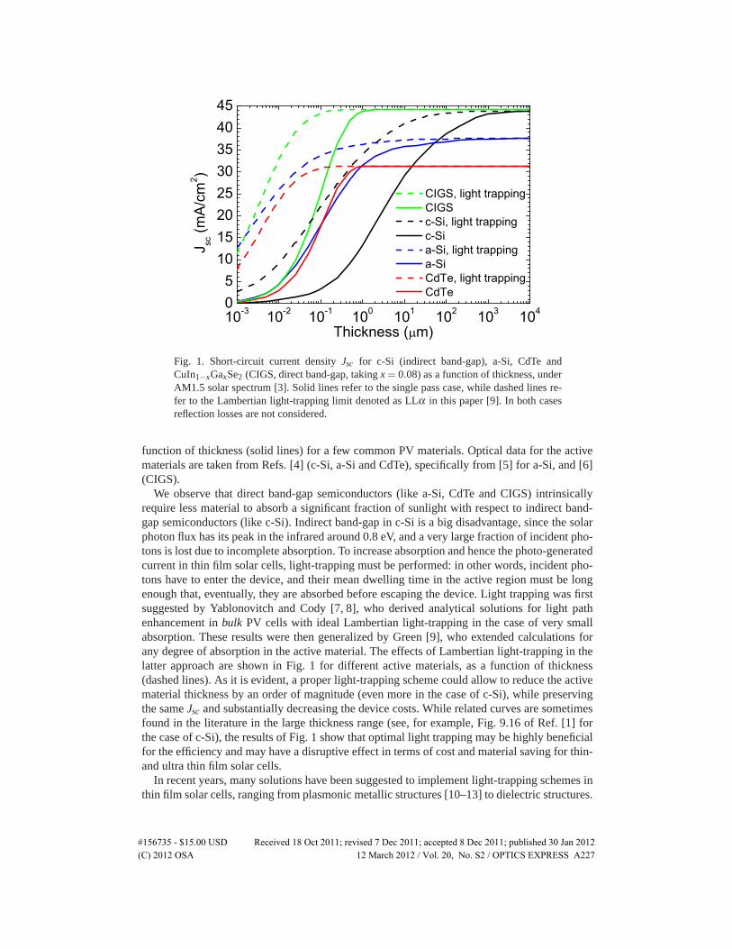
Fig. 1. Short-circuit current density Jsc for c-Si (indirect band-gap), a-Si, CdTe andCuIn1−xGaxSe2 (CIGS, direct band-gap, taking x = 0.08) as a function of thickness, underAM1.5 solar spectrum [3]. Solid lines refer to the single pass case, while dashed lines re-fer to the Lambertian light-trapping limit denoted as LLα in this paper [9]. In both casesreflection losses are not considered.
function of thickness (solid lines) for a few common PV materials. Optical data for the activematerials are taken from Refs. [4] (c-Si, a-Si and CdTe), specifically from [5] for a-Si, and [6](CIGS).
We observe that direct band-gap semiconductors (like a-Si, CdTe and CIGS) intrinsicallyrequire less material to absorb a significant fraction of sunlight with respect to indirect band-gap semiconductors (like c-Si). Indirect band-gap in c-Si is a big disadvantage, since the solarphoton flux has its peak in the infrared around 0.8 eV, and a very large fraction of incident pho-tons is lost due to incomplete absorption. To increase absorption and hence the photo-generatedcurrent in thin film solar cells, light-trapping must be performed: in other words, incident pho-tons have to enter the device, and their mean dwelling time in the active region must be longenough that, eventually, they are absorbed before escaping the device. Light trapping was firstsuggested by Yablonovitch and Cody [7, 8], who derived analytical solutions for light pathenhancement in bulk PV cells with ideal Lambertian light-trapping in the case of very smallabsorption. These results were then generalized by Green [9], who extended calculations forany degree of absorption in the active material. The effects of Lambertian light-trapping in thelatter approach are shown in Fig. 1 for different active materials, as a function of thickness(dashed lines). As it is evident, a proper light-trapping scheme could allow to reduce the activematerial thickness by an order of magnitude (even more in the case of c-Si), while preservingthe same Jsc and substantially decreasing the device costs. While related curves are sometimesfound in the literature in the large thickness range (see, for example, Fig. 9.16 of Ref. [1] forthe case of c-Si), the results of Fig. 1 show that optimal light trapping may be highly beneficialfor the efficiency and may have a disruptive effect in terms of cost and material saving for thin-and ultra thin film solar cells.
In recent years, many solutions have been suggested to implement light-trapping schemes inthin film solar cells, ranging from plasmonic metallic structures [10–13] to dielectric structures.
#156735 - $15.00 USD Received 18 Oct 2011; revised 7 Dec 2011; accepted 8 Dec 2011; published 30 Jan 2012(C) 2012 OSA 12 March 2012 / Vol. 20, No. S2 / OPTICS EXPRESS A227
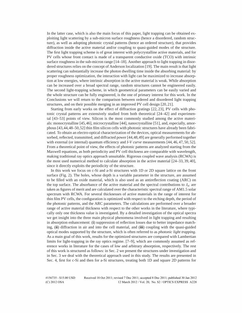
In the latter case, which is also the main focus of this paper, light trapping can be obtained ex-ploiting light scattering by a sub-micron surface roughness (hence a disordered, random struc-ture), as well as adopting photonic crystal patterns (hence an ordered structure), that providesdiffraction inside the active material and/or coupling to quasi-guided modes of the structure.The first light trapping scheme is of great interest with polycrystalline active materials, and forPV cells whose front contact is made of a transparent conductive oxide (TCO) with intrinsicsurface roughness in the sub-micron range [14–18]. Another approach to light trapping in disor-dered structures relies on the concept of Anderson localization [19]. The main result is that lightscattering can substantially increase the photon dwelling time inside the absorbing material: byproper roughness optimization, the interaction with light can be maximized to increase absorp-tion at low energies, where intrinsic absorption in the active material is weak. While absorptioncan be increased over a broad spectral range, random structures cannot be engineered easily.The second light-trapping scheme, in which geometrical parameters can be easily varied andthe whole structure can be fully engineered, is the one of primary interest for this work. In theConclusions we will return to the comparison between ordered and disordered light trappingstructures, and on their possible merging in an improved PV cell design [20, 21].
Starting from early works on the effect of diffraction gratings [22, 23], PV cells with pho-tonic crystal patterns are extensively studied from both theoretical [24–42] and experimen-tal [43–53] points of view. Silicon is the most commonly studied among the active materi-als: monocrystalline [45,46], microcrystalline [44], nanocrystalline [51], and, especially, amor-phous [43,44,48–50,52] thin film silicon cells with photonic structures have already been fabri-cated. To obtain an electro-optical characterization of the devices, optical measurements for ab-sorbed, reflected, transmitted, and diffracted power [44,48,49] are generally performed togetherwith external (or internal) quantum efficiency and I-V curve measurements [44, 46, 47, 50, 52].From a theoretical point of view, the effects of photonic patterns are analyzed starting from theMaxwell equations, as both periodicity and PV cell thickness are comparable with wavelength,making traditional ray optics approach unsuitable. Rigorous coupled wave analysis (RCWA) isthe most used numerical method to calculate absorption in the active material [24–33, 39, 40],since it directly exploits the periodicity of the structure.
In this work we focus on c-Si and a-Si structures with 1D or 2D square lattice on the frontsurface (Fig. 2). The holes, whose depth is a variable parameter in the structure, are assumedto be filled with an oxide material, which is also used as an antireflection coating (ARC) onthe top surface. The absorbance of the active material and the spectral contributions to Jsc aretaken as figures of merit and are calculated over the characteristic spectral range of AM1.5 solarspectrum with RCWA. For several thicknesses of active materials in the range of interest forthin film PV cells, the configuration is optimized with respect to the etching depth, the period ofthe photonic patterns, and the ARC parameters. The calculations are performed over a broaderrange of active material thickness with respect to the other works in the literature, where typi-cally only one thickness value is investigated. By a detailed investigation of the optical spectrawe get insight into the three main physical phenomena involved in light trapping and resultingin absorption enhancement: (i) suppression of reflection losses due to better impedance match-ing, (ii) diffraction in air and into the cell material, and (iii) coupling with the quasi-guidedoptical modes supported by the structure, which is often referred to as photonic light trapping.As a main goal of this work, results for the optimized structures are compared with Lambertianlimits for light-trapping in the ray optics regime. [7–9], which are commonly assumed as ref-erence works in literature for the cases of low and arbitrary absorption, respectively. The restof this work is structured as follows: in Sec. 2 we present the structures under investigation andin Sec. 3 we deal with the theoretical approach used in this study. The results are presented inSec. 4, first for c-Si and then for a-Si structures, treating both 1D and square 2D patterns for
#156735 - $15.00 USD Received 18 Oct 2011; revised 7 Dec 2011; accepted 8 Dec 2011; published 30 Jan 2012(C) 2012 OSA 12 March 2012 / Vol. 20, No. S2 / OPTICS EXPRESS A228
Fig. 2. Scheme of silicon PV cells patterned with a simple 1D photonic lattice (a) and witha square 2D lattice (b).
each material. Conclusions and prospective developments are summarized in Sec. 5.
2. Analyzed structures
The structures analyzed in this work are PV cells patterned with a 1D or with a square 2Dlattice, as shown in Figs. 2(a) and 2(b), respectively. The PV cell surface is taken in the (x,y)plane, with z the direction normal to the cell. The direction of incident radiation is indicated bythe red arrow in Fig. 2(a) and can be identified with the pair of polar angle θ and azimuthalangle φ . For the present work, we limit ourselves to nearly normal incidence, namely θ=0.1◦and φ=0◦ (the choice θ=0.1◦ is necessary for the convergence of the calculations and it doesnot substantially modify the results from the normal incidence case, [54]). The results are av-eraged over the two, orthogonal polarizations. We previously analyzed the dependence of thecell response on the incidence direction and polarization [36], and we found that these struc-tures are rather robust with respect to variations in both θ and φ . This is particularly interestingin the case of 1D patterns, since a stronger angular dependence would be expected. Instead, atypical cosθ dependence of the current response was found, and the same trend occurs whenthe polarization direction is parallel (φ=0) or orthogonal (φ=90 degrees) to the grating [36].For 2D structures, the angular dependence is expected to be further suppressed, due to highersymmetry and isotropy.
Both 1D and 2D patterns are supposed to be obtained via etching procedure starting from aslab of semiconductor material of thickness d, deposited on a silver (for optical data see Ref.[4]) substrate that serves as back reflector and electric contact. The active materials we considerare c-Si and a-Si, whose optical functions are taken from Ref. [4]. The spectral absorbances ofthese materials are different, and this affects the typical thickness d required to obtain completelight absorption, making c-Si PV cells much thicker than a-Si ones. Being interested in light-trapping in thin film Si solar cells, we limit the range of thicknesses from 250 nm to 4 μm forc-Si PV cells and from 50 to 500 nm for a-Si PV cells. Especially for the case of a-Si PV cells,the film thickness is limited by diffusion lengths for the photogenerated carriers, which are lessthan a few hundreds nanometres [2].
For PV cells with 1D pattern, the period is indicated with a, the width of the etched regionwith b, and the etching depth with h. The grooves are supposed to be filled with a transparentdielectric medium with refractive index nARC=1.65, and the same dielectric is supposed to be
#156735 - $15.00 USD Received 18 Oct 2011; revised 7 Dec 2011; accepted 8 Dec 2011; published 30 Jan 2012(C) 2012 OSA 12 March 2012 / Vol. 20, No. S2 / OPTICS EXPRESS A229
deposited until a covering slab of thickness l is formed. This layer acts both as a passivatingstructure for the etched layer as well as an anti-reflection coating (ARC). The value for nARC
is in between that of fused silica (SiO2, see Ref. [4] for optical data) and that of transparentconductive oxides, as, for example, Al-doped zinc oxide (AZO, see Ref. [56]) and indiumtin oxide (ITO, see Ref. [57]). In this way our results are generally applicable without strongvariations to PV cells whose patterned layers have very different transport properties, frompassivating window layers (for example with SiO2, as we used in our previous work [33,36]) toconductive layers for carriers extraction. In this work we choose an idealized, dispersion-less,covering dielectric, but more realistic and absorbing materials could be considered withoutmajor changes to the conclusions. The thickness of the covering slab l is set to 70 nm for all theinvestigated structures: this value has been optimized in a previous work on 1D lattices [33],and we have verified that the same optimized value is found for the 2D lattices considered inthis work.
For PV cells with a 2D square pattern (Fig. 2(b)), the same notation is used for the latticeperiod, the ARC thickness, and the etching depth. In this case we consider a 2D lattice ofcircular rods of radius r etched in the Si slab, and the materials filling fractions are
FFSi = 1− πr2
a2 FFARC =πr2
a2 . (1)
We shall display the results as a function of the ratio r/a (instead of the filling parameters FF),as it gives a more intuitive description of the pattern structure. Attention should be paid to thefact that the ratio b/a for 1D patterns can span the range [0,1], while the ratio r/a is within therange [0,0.5], the upper limit corresponding to rods’ contact.
We analyzed also another 2D periodic pattern, namely the triangular lattice of circular rods.We found that best results for triangular pattern are essentially analogous to those for squarepattern, as expected from the high symmetry of both lattices. However, rather unexpectedly, thesquare lattice gives slightly higher short-circuit currents than the triangular lattice. In view ofthis, in the rest of this paper we present only the results for square patterns.
3. Theory and numerical methods
The electric response of a PV cell is given by its current-to-voltage curve or, more briefly, I-V curve. From a theoretical point of view, this relation can be derived assuming an ideal andexponential I-V curve for the p-n junction forming the PV cell and adding a current contributionproportional to the flux of incident photons with energy larger than the band-gap Eg (Ref. [1]).Considering the response of the PV cell unit area rather than that of the whole PV cell, the J-Vcurve can be expressed as:
J(V ) = Jsc − J0
[e
eVKBT −1
], (2)
where Jsc is the short-circuit current density, J0 is the generation current density for the p-njunction, e the electron charge, KB the Boltzmann constant, and T the thermalized electrontemperature of the cell. At a given operating voltage V , the product V ·J(V ) gives the electricalpower converted by PV cell per unit area. It can be shown that this depends nearly linearlyupon Jsc, and for this reason Jsc has been assumed as our main figure of merit. The short-circuitcurrent density Jsc is a spectrally-integrated quantity defined as [1]:
Jsc = e∫ ∞
Eg
A(E)dN
dEIQE(E)dE ≡
e∫ ∞
Eg
A(E)dN
dEdE ≡
∫ ∞
Eg
dJsc(E)dE
dE, (3)
#156735 - $15.00 USD Received 18 Oct 2011; revised 7 Dec 2011; accepted 8 Dec 2011; published 30 Jan 2012(C) 2012 OSA 12 March 2012 / Vol. 20, No. S2 / OPTICS EXPRESS A230
where A(E) is the absorbance of the active material, dNdE is the incident solar photon flux (which
has dimension of number of incident photons per unit time, per unit surface area, and per unitenergy bandwidth), and IQE is the internal quantum efficiency for separation and collection ofthe photogenerated electron-hole pairs. Since in this work we are concerned with the opticalrather than transport properties of the cell, IQE has been set equal to one. In this way one candefine the spectral contribution dJsc/dE to the short-circuit current density (Eq. (3)). This inturn is proportional to the absorbance A(E) of the active material in the PV cell, which is takenas our second figure of merit. The integration range has a lower limit 1.12 eV for c-Si, or 1.25eV for a-Si (the bandgap of a-Si with the data of Ref. [5]). The upper limit is taken to be 3.5eV in both cases, as the photon flux above this energy is small in the standard AM1.5 solarspectrum [3]. Finally, as in our previous work [33], a black-body dependence is assumed forthe photon flux dN
dE , with characteristic emission temperature of 5800 K and total irradiance of100 mW/cm2, which is that of the AM1.5 solar spectrum. Both the truncation of the integrationrange and the choice of a blackbody spectrum affect the final results, giving lower Jsc withrespect to the full AM1.5 solar spectrum, which is slightly richer in photons in the visiblerange. This is the reason why the subsequent results for Lambertian limits are slightly smallerthan those given in Fig. 1: this choice allows to considerably reduce computing time whenoptimizing the structures. Of course, a real solar cell should be simulated with the full AM1.5spectrum.
The absorbance A(E) of the active layer and hence Jsc are calculated adopting a rigorouselectromagnetic approach, starting from Maxwell equations for fields E(x,y,z) and H(x,y,z),and then calculating the scattering matrix S for the configuration under investigation [54, 55].The PV structure is treated as a multilayer along z (see Fig. 3(a)), with the light incident fromthe left, under the form of a plane wave. Following the notations of Refs. [33] and [54], anddenoting in-plane coordinates (x,y) ≡ ρ , the electric field E can be expressed in each point asa Fourier series:
E(ρ,z) =NPW−1
∑n=0
E(Gn,z)ei(k//+Gn)·ρ , (4)
where NPW is the total number of plane waves considered in the simulation, Gn are the recip-rocal lattice vectors (taking G0 = 0), and k// is the component of incident wave vector in the(x,y) plane. The Fourier amplitudes E(Gn,z) are obtained solving Maxwell equations in eachlayer by matrix diagonalization, and then propagating along the structure with proper boundaryconditions, with the basis set of plane waves determined by NPW (z dependence is implicitlytaken into account, with both propagating and exponentially decaying waves being considered).
Due to translational invariance, we can limit ourselves to the unit cell in the (x,y) plane, andapply Poynting theorem to the volume element enclosed by dashed line in Fig. 3(a). Absorptionin the active material is calculated from difference in Poynting vector fluxes across the facetsnormal to z direction, while any contributions from the other facets vanish due to translationalinvariance. Normalizing incident power density to unit, energetic balance implies:
A+R+T + ∑n�=0
Rn + ∑n�=0
Tn = 1, (5)
where A is the absorbance of the active material, R = Rn=0 is the zeroth-order reflectance, andT = Tn=0 is the zeroth-order transmittance to the Ag substrate. The first sum represents all thepower contributions deriving from diffraction in air, and the second sum refers to diffractionin the Ag substrate. In the case of a planar cell, the last two sums in Eq. (5) are absent, due totranslational invariance, and thus R and T are the only optical losses (Eq. (5) simply reduces toA+R+T=1).
#156735 - $15.00 USD Received 18 Oct 2011; revised 7 Dec 2011; accepted 8 Dec 2011; published 30 Jan 2012(C) 2012 OSA 12 March 2012 / Vol. 20, No. S2 / OPTICS EXPRESS A231
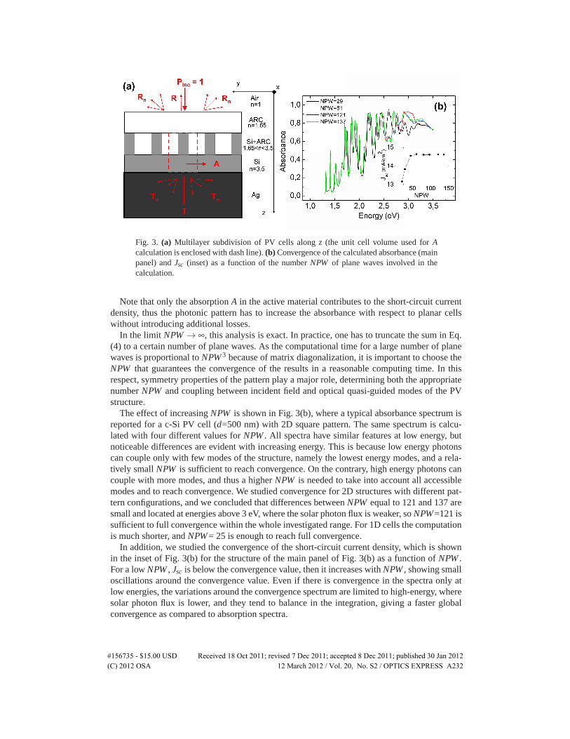
Fig. 3. (a) Multilayer subdivision of PV cells along z (the unit cell volume used for Acalculation is enclosed with dash line). (b) Convergence of the calculated absorbance (mainpanel) and Jsc (inset) as a function of the number NPW of plane waves involved in thecalculation.
Note that only the absorption A in the active material contributes to the short-circuit currentdensity, thus the photonic pattern has to increase the absorbance with respect to planar cellswithout introducing additional losses.
In the limit NPW → ∞, this analysis is exact. In practice, one has to truncate the sum in Eq.(4) to a certain number of plane waves. As the computational time for a large number of planewaves is proportional to NPW 3 because of matrix diagonalization, it is important to choose theNPW that guarantees the convergence of the results in a reasonable computing time. In thisrespect, symmetry properties of the pattern play a major role, determining both the appropriatenumber NPW and coupling between incident field and optical quasi-guided modes of the PVstructure.
The effect of increasing NPW is shown in Fig. 3(b), where a typical absorbance spectrum isreported for a c-Si PV cell (d=500 nm) with 2D square pattern. The same spectrum is calcu-lated with four different values for NPW . All spectra have similar features at low energy, butnoticeable differences are evident with increasing energy. This is because low energy photonscan couple only with few modes of the structure, namely the lowest energy modes, and a rela-tively small NPW is sufficient to reach convergence. On the contrary, high energy photons cancouple with more modes, and thus a higher NPW is needed to take into account all accessiblemodes and to reach convergence. We studied convergence for 2D structures with different pat-tern configurations, and we concluded that differences between NPW equal to 121 and 137 aresmall and located at energies above 3 eV, where the solar photon flux is weaker, so NPW=121 issufficient to full convergence within the whole investigated range. For 1D cells the computationis much shorter, and NPW= 25 is enough to reach full convergence.
In addition, we studied the convergence of the short-circuit current density, which is shownin the inset of Fig. 3(b) for the structure of the main panel of Fig. 3(b) as a function of NPW .For a low NPW , Jsc is below the convergence value, then it increases with NPW , showing smalloscillations around the convergence value. Even if there is convergence in the spectra only atlow energies, the variations around the convergence spectrum are limited to high-energy, wheresolar photon flux is lower, and they tend to balance in the integration, giving a faster globalconvergence as compared to absorption spectra.
#156735 - $15.00 USD Received 18 Oct 2011; revised 7 Dec 2011; accepted 8 Dec 2011; published 30 Jan 2012(C) 2012 OSA 12 March 2012 / Vol. 20, No. S2 / OPTICS EXPRESS A232
We compared our results with Lambertian limits to light trapping in bulk PV cells. The upperlimits for the enhancement of light path inside the active material were first derived under threeassumptions [7, 8]:
• The structure has a front Lambertian scatterer or a back Lambertian reflector on thebottom. In both cases transmitted or reflected light is randomized with isotropic angulardistribution at every energy. Furthermore, intrinsic reflection losses of the active materialare set to zero, and an ideal back reflector is located at the bottom.
• The intrinsic absorption of the active material is sufficiently low for both the single-passand the enhanced absorbance. This situation is referred to as weak absorption regime andis described by the condition:
4n2αd � 1, (6)
where n is the real part of the refractive index, α is the absorption coefficient, and d thethickness of the active material.
• The film thickness d is much larger than wavelength λ/n inside the active material, andthis makes ray optics arguments suitable.
The absorption can thus be described and quantified in terms of the product α(E)deff, with deff
being the effective light path inside the active material in a given configuration. For example, ifwe consider a single-pass through a planar slab, neglecting reflection losses, the product αdeff
has a direct interpretation, as the total absorbance Asp is:
Asp(E) = 1− e−α(E)d . (7)
Under Yablonovitch hypothesis, it can be shown using ray optics or statistical mechanics argu-ments that the maximum light path is enhanced by a factor 4n2/sin2γ , with γ half of the apexangle of the cone subtended by the dielectric medium surrounding the cell. In the case of a pla-nar cell surrounded by an isotropic medium (sinγ=1), the maximum enhancement is given by4n2, which corresponds to nearly 50 for silicon near the band gap and gives an active materialabsorbance equal to:
ALL0(E) = 1− e−4n2α(E)d , (8)
where reflection losses are neglected. Along the manuscript, this first Lambertian limit (i.e.,weak absorption and neglecting reflection losses) will be denoted by LL0.
More recently, a general limit to Lambertian light-trapping has been derived by Green con-sidering the case of arbitrary absorption and providing an analytic expression for light pathenhancement as a function of the photon energy [9]. In this case, assuming sinγ=1, it can beshown that the maximum absorption enhancement is lower than in the LL0 limit, as the weakabsorption hypothesis is relaxed and the enhancement expected by light trapping is smallerwhen absorption is larger. We refer to [9] for details of the theoretical treatment. This generalLambertian limit will be denoted by LLα , and it is the most relevant for our work, since activematerial’s absorption is not negligible in most of the investigated configurations. To compareproperly with the LL0 limit, we take also the LLα limit in the case of no reflection losses.
Both light trapping limits investigated by Yablonovitch and Green are valid in the limit of rayoptics, i.e., they assume that the active material thickness is much larger than the wavelength oflight. In the present study, the typical dimensions of thin-film solar cells are comparable to thewavelength of light in most of the spectral range. In the literature this situation is often referredto as photonic light-trapping, in contrast with the case of bulk PV cells. Light trapping in the(nano)photonic regime has been investigated in Refs. [31, 32] for the case of weak absorption,
#156735 - $15.00 USD Received 18 Oct 2011; revised 7 Dec 2011; accepted 8 Dec 2011; published 30 Jan 2012(C) 2012 OSA 12 March 2012 / Vol. 20, No. S2 / OPTICS EXPRESS A233
where it is shown that the LL0 limit can be overcome in some circumstances. Still, the generallimit to light trapping for any material thickness and for arbitrary absorption is unknown. Herewe shall take the LL0 and LLα limits as references for the calculated short-circuit current andabsorbance spectra, since they can be easily calculated and provide a continuous transition tothe case of thick cells, where the ray optics treatment is rigorously valid. In fact, the dashedcurves of Fig. 1 are calculated for the realistic case of the LLα limit.
In the case of photonic light-trapping, it is difficult to introduce an effective light path. Thuswe define an absorption enhancement factor F with respect to the single pass absorption Asp as
F(E) =A(E)
Asp(E)=
A(E)
1− e−α(E)d, (9)
where A(E) is the structure absorption, which can be calculated analytically or numericallydepending on the cell geometry. It is worth noticing that the two limits discussed above canbe described using Eq. (9). In particular, in the case of weak absorption the expression givesback the typical 4n2 enhancement factor, which can be considered as a reference value forLambertian light trapping. As it will be evident from the results in the next section, reachingLambertian light-trapping limits over a broad spectral range is a very difficult task, which canbe partly (but not fully) achieved with the periodic structures considered in this work.
4. Results and discussion
We analyze separately the properties of c-Si and a-Si PV cells patterned with photonic lattices.1D and square 2D patterns are compared for several thicknesses d in range of interest for thinfilm solar cells, according to observations of Sect. 2. For brevity, only one thickness is analyzedin detail for each active material (1 μm for c-Si and 300 nm for a-Si), and the results forstructures of varying thickness are described at the end of each material’s subsection.
At a fixed active material thickness d, the analysis is performed in the following way. First, acontour plot of Jsc is calculated with the scattering matrix formalism varying at the same timethe etching depth h and the ratio b/a (for 1D pattern) or r/a (for square pattern). Accordingto observations of Sec. 3, the number NPW of plane waves is chosen to be 45 for 2D squarepattern. Optimal pattern configurations are then identified from maxima in the contour plot,and the corresponding spectra are analyzed in detail. For each optimal configuration, opticalspectra for reflectance R, transmittance T , absorbance A, and diffracted power are calculatedwith a NPW that ensures convergence over the whole spectrum (NPW=25 for 1D patters and121 for 2D square patterns). Finally, the absorption enhancement F with respect to single passabsorption without reflection losses is compared with the Lambertian limits LL0 and LLα tolight-trapping.
Some relevant reference spectra for A and Jsc are considered. For absorbance, the comparisonis made with the absorbance of a bare slab of active material, without ARC or back reflectorand considering the cases with and without reflection losses. This comparison is useful becauseit directly recalls intrinsic properties of the active material in terms of bare absorption andreflection. The energy range for calculations can thus be subdivided into two ranges: one at lowenergy, where patterning enhances absorption due to light-trapping, and the other one at highenergy, where total absorption occurs even without light-trapping, and, actually, reflection anddiffraction in air have to be minimized.
For short-circuit current density Jsc and spectral contributions dJsc/dE, the comparison ismade with a reference cell with same thickness d of the investigated configuration, planar ge-ometry, Ag back reflector, and single-layer ARC on top. Optical spectra for reference cells arecalculated following the same procedure used for patterned cells. The parameters of the ARC
#156735 - $15.00 USD Received 18 Oct 2011; revised 7 Dec 2011; accepted 8 Dec 2011; published 30 Jan 2012(C) 2012 OSA 12 March 2012 / Vol. 20, No. S2 / OPTICS EXPRESS A234
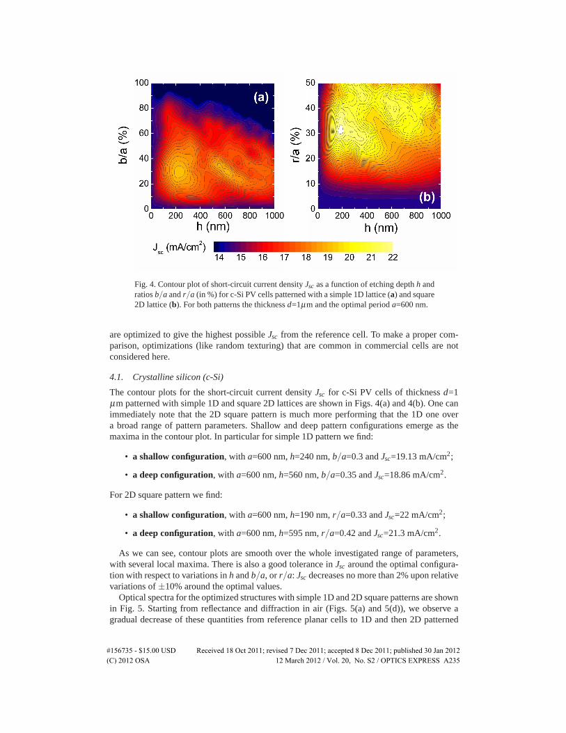
Fig. 4. Contour plot of short-circuit current density Jsc as a function of etching depth h andratios b/a and r/a (in %) for c-Si PV cells patterned with a simple 1D lattice (a) and square2D lattice (b). For both patterns the thickness d=1μm and the optimal period a=600 nm.
are optimized to give the highest possible Jsc from the reference cell. To make a proper com-parison, optimizations (like random texturing) that are common in commercial cells are notconsidered here.
4.1. Crystalline silicon (c-Si)
The contour plots for the short-circuit current density Jsc for c-Si PV cells of thickness d=1μm patterned with simple 1D and square 2D lattices are shown in Figs. 4(a) and 4(b). One canimmediately note that the 2D square pattern is much more performing that the 1D one overa broad range of pattern parameters. Shallow and deep pattern configurations emerge as themaxima in the contour plot. In particular for simple 1D pattern we find:
• a shallow configuration, with a=600 nm, h=240 nm, b/a=0.3 and Jsc=19.13 mA/cm2;
• a deep configuration, with a=600 nm, h=560 nm, b/a=0.35 and Jsc=18.86 mA/cm2.
For 2D square pattern we find:
• a shallow configuration, with a=600 nm, h=190 nm, r/a=0.33 and Jsc=22 mA/cm2;
• a deep configuration, with a=600 nm, h=595 nm, r/a=0.42 and Jsc=21.3 mA/cm2.
As we can see, contour plots are smooth over the whole investigated range of parameters,with several local maxima. There is also a good tolerance in Jsc around the optimal configura-tion with respect to variations in h and b/a, or r/a: Jsc decreases no more than 2% upon relativevariations of ±10% around the optimal values.
Optical spectra for the optimized structures with simple 1D and 2D square patterns are shownin Fig. 5. Starting from reflectance and diffraction in air (Figs. 5(a) and 5(d)), we observe agradual decrease of these quantities from reference planar cells to 1D and then 2D patterned
#156735 - $15.00 USD Received 18 Oct 2011; revised 7 Dec 2011; accepted 8 Dec 2011; published 30 Jan 2012(C) 2012 OSA 12 March 2012 / Vol. 20, No. S2 / OPTICS EXPRESS A235
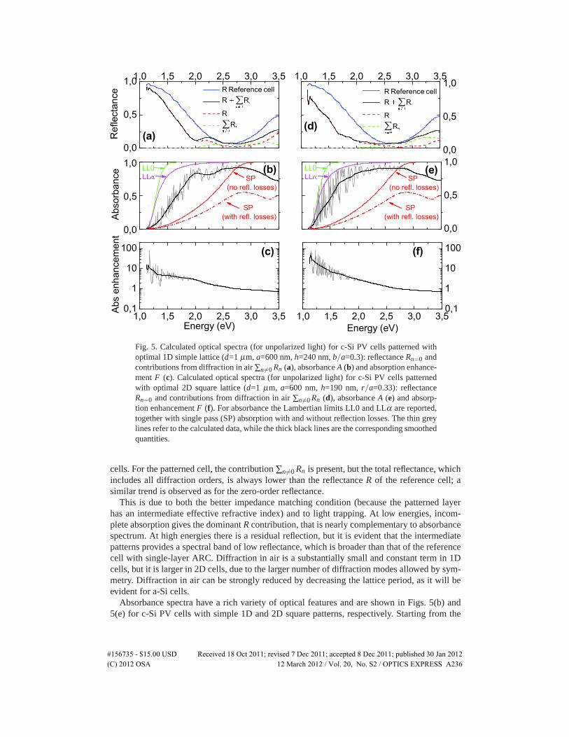
Fig. 5. Calculated optical spectra (for unpolarized light) for c-Si PV cells patterned withoptimal 1D simple lattice (d=1 μm, a=600 nm, h=240 nm, b/a=0.3): reflectance Rn=0 andcontributions from diffraction in air ∑n�=0 Rn (a), absorbance A (b) and absorption enhance-ment F (c). Calculated optical spectra (for unpolarized light) for c-Si PV cells patternedwith optimal 2D square lattice (d=1 μm, a=600 nm, h=190 nm, r/a=0.33): reflectanceRn=0 and contributions from diffraction in air ∑n�=0 Rn (d), absorbance A (e) and absorp-tion enhancement F (f). For absorbance the Lambertian limits LL0 and LLα are reported,together with single pass (SP) absorption with and without reflection losses. The thin greylines refer to the calculated data, while the thick black lines are the corresponding smoothedquantities.
cells. For the patterned cell, the contribution ∑n�=0 Rn is present, but the total reflectance, whichincludes all diffraction orders, is always lower than the reflectance R of the reference cell; asimilar trend is observed as for the zero-order reflectance.
This is due to both the better impedance matching condition (because the patterned layerhas an intermediate effective refractive index) and to light trapping. At low energies, incom-plete absorption gives the dominant R contribution, that is nearly complementary to absorbancespectrum. At high energies there is a residual reflection, but it is evident that the intermediatepatterns provides a spectral band of low reflectance, which is broader than that of the referencecell with single-layer ARC. Diffraction in air is a substantially small and constant term in 1Dcells, but it is larger in 2D cells, due to the larger number of diffraction modes allowed by sym-metry. Diffraction in air can be strongly reduced by decreasing the lattice period, as it will beevident for a-Si cells.
Absorbance spectra have a rich variety of optical features and are shown in Figs. 5(b) and5(e) for c-Si PV cells with simple 1D and 2D square patterns, respectively. Starting from the
#156735 - $15.00 USD Received 18 Oct 2011; revised 7 Dec 2011; accepted 8 Dec 2011; published 30 Jan 2012(C) 2012 OSA 12 March 2012 / Vol. 20, No. S2 / OPTICS EXPRESS A236

Fig. 6. Spectral contributions dJsc/dE to short-circuit current density Jsc for c-Si PV cellspatterned with optimized 1D and square 2D square lattices. Thickness d=1μm, optimalperiod a=600 nm.
single pass case, we note that a planar slab of thickness d=1 μm has the potential to absorbnearly all incident light with energy greater than 2.75 eV, at least when a proper ARC is appliedon the front surface. Light trapping has to be tailored to give its maximum contribution belowthis energy threshold. This is done optimizing the structures, and best results reported in Figs.5(b) and 5(e) show several peaks deriving from coupling with quasi-guided modes. Since thetypical spectral width of each peak is narrow compared to the useful solar spectrum bandwidth,a collection from multiple peaks deriving from different coupling processes is needed to obtainrelevant increase in Jsc.
Due to the higher number of quasi-guided modes available related to higher symmetry, 2Dpatterns are always better than 1D ones. For both patterns, the line shape of the resonancebroadens for increasing energy, according to the fact that a higher intrinsic absorption produceslower and broader features in the absorption spectra [31, 32].
For c-Si cells with 1D pattern, the calculated absorbance is always lower than both LL0and LLα limits. This is evident from absorption enhancement F reported in Fig. 5(c), whichreaches a smoothed maximum value of 15, still far away from 4n2 maximum value for theLL0 limit in the weak absorption regime. For c-Si PV cells with 2D square lattice, instead, thecalculated absorbance can overcome both LL0 and LLα limits, at least at the exact energies forcoupling with quasi-guided modes, in agreement with predictions from temporal coupled-modetheory [31, 32]. When absorption enhancement is smoothed, the maximum value reaches 40 to45 near the c-Si band gap energy, not far away from 4n2 for Lambertian limit to light-trapping(Fig. 5(f)).
Smoothed spectral contributions dJsc/dE to short-circuit current density are shown in Fig. 6.In terms of short-circuit current density, patterning gives a +30% enhancement for the 1D case,and a +55% enhancement for the 2D square case, compared to a reference cell with the samethickness d=1 μm.
In order to check the validity of our optimization procedure, we compared our results withothers in literature that are available for the same structures at a few specific thicknesses. Forexample, Refs. [29, 40] reported results about 1 μm thick microcrystalline Si PV cells withfrontal 1D grating and back reflector, with optimal period a=600 nm and optimal grating height
#156735 - $15.00 USD Received 18 Oct 2011; revised 7 Dec 2011; accepted 8 Dec 2011; published 30 Jan 2012(C) 2012 OSA 12 March 2012 / Vol. 20, No. S2 / OPTICS EXPRESS A237
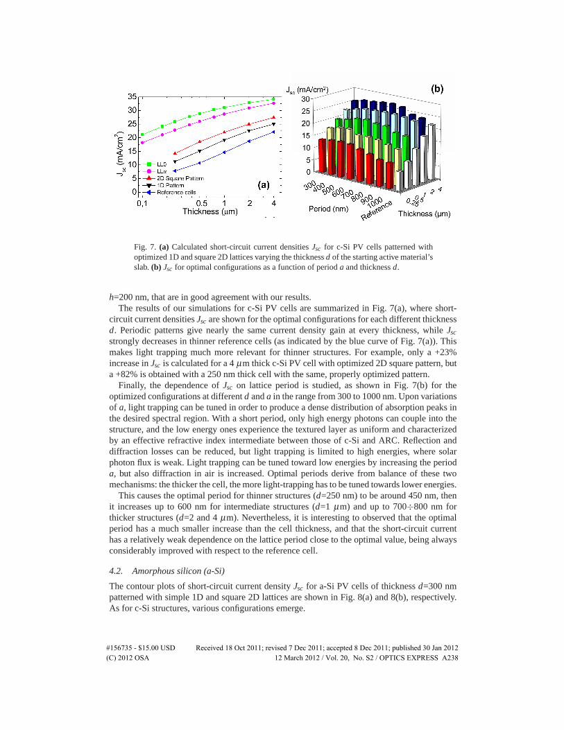
Fig. 7. (a) Calculated short-circuit current densities Jsc for c-Si PV cells patterned withoptimized 1D and square 2D lattices varying the thickness d of the starting active material’sslab. (b) Jsc for optimal configurations as a function of period a and thickness d.
h=200 nm, that are in good agreement with our results.The results of our simulations for c-Si PV cells are summarized in Fig. 7(a), where short-
circuit current densities Jsc are shown for the optimal configurations for each different thicknessd. Periodic patterns give nearly the same current density gain at every thickness, while Jsc
strongly decreases in thinner reference cells (as indicated by the blue curve of Fig. 7(a)). Thismakes light trapping much more relevant for thinner structures. For example, only a +23%increase in Jsc is calculated for a 4 μm thick c-Si PV cell with optimized 2D square pattern, buta +82% is obtained with a 250 nm thick cell with the same, properly optimized pattern.
Finally, the dependence of Jsc on lattice period is studied, as shown in Fig. 7(b) for theoptimized configurations at different d and a in the range from 300 to 1000 nm. Upon variationsof a, light trapping can be tuned in order to produce a dense distribution of absorption peaks inthe desired spectral region. With a short period, only high energy photons can couple into thestructure, and the low energy ones experience the textured layer as uniform and characterizedby an effective refractive index intermediate between those of c-Si and ARC. Reflection anddiffraction losses can be reduced, but light trapping is limited to high energies, where solarphoton flux is weak. Light trapping can be tuned toward low energies by increasing the perioda, but also diffraction in air is increased. Optimal periods derive from balance of these twomechanisms: the thicker the cell, the more light-trapping has to be tuned towards lower energies.
This causes the optimal period for thinner structures (d=250 nm) to be around 450 nm, thenit increases up to 600 nm for intermediate structures (d=1 μm) and up to 700÷800 nm forthicker structures (d=2 and 4 μm). Nevertheless, it is interesting to observed that the optimalperiod has a much smaller increase than the cell thickness, and that the short-circuit currenthas a relatively weak dependence on the lattice period close to the optimal value, being alwaysconsiderably improved with respect to the reference cell.
4.2. Amorphous silicon (a-Si)
The contour plots of short-circuit current density Jsc for a-Si PV cells of thickness d=300 nmpatterned with simple 1D and square 2D lattices are shown in Fig. 8(a) and 8(b), respectively.As for c-Si structures, various configurations emerge.
#156735 - $15.00 USD Received 18 Oct 2011; revised 7 Dec 2011; accepted 8 Dec 2011; published 30 Jan 2012(C) 2012 OSA 12 March 2012 / Vol. 20, No. S2 / OPTICS EXPRESS A238
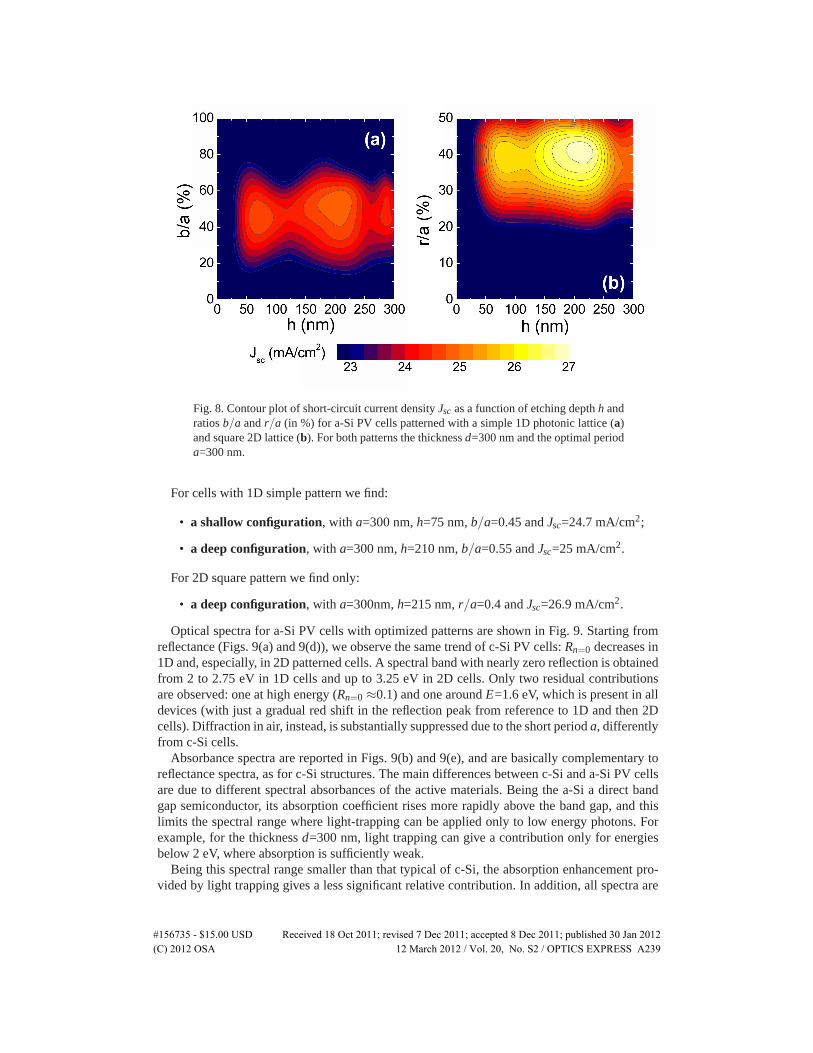
Fig. 8. Contour plot of short-circuit current density Jsc as a function of etching depth h andratios b/a and r/a (in %) for a-Si PV cells patterned with a simple 1D photonic lattice (a)and square 2D lattice (b). For both patterns the thickness d=300 nm and the optimal perioda=300 nm.
For cells with 1D simple pattern we find:
• a shallow configuration, with a=300 nm, h=75 nm, b/a=0.45 and Jsc=24.7 mA/cm2;
• a deep configuration, with a=300 nm, h=210 nm, b/a=0.55 and Jsc=25 mA/cm2.
For 2D square pattern we find only:
• a deep configuration, with a=300nm, h=215 nm, r/a=0.4 and Jsc=26.9 mA/cm2.
Optical spectra for a-Si PV cells with optimized patterns are shown in Fig. 9. Starting fromreflectance (Figs. 9(a) and 9(d)), we observe the same trend of c-Si PV cells: Rn=0 decreases in1D and, especially, in 2D patterned cells. A spectral band with nearly zero reflection is obtainedfrom 2 to 2.75 eV in 1D cells and up to 3.25 eV in 2D cells. Only two residual contributionsare observed: one at high energy (Rn=0 ≈0.1) and one around E=1.6 eV, which is present in alldevices (with just a gradual red shift in the reflection peak from reference to 1D and then 2Dcells). Diffraction in air, instead, is substantially suppressed due to the short period a, differentlyfrom c-Si cells.
Absorbance spectra are reported in Figs. 9(b) and 9(e), and are basically complementary toreflectance spectra, as for c-Si structures. The main differences between c-Si and a-Si PV cellsare due to different spectral absorbances of the active materials. Being the a-Si a direct bandgap semiconductor, its absorption coefficient rises more rapidly above the band gap, and thislimits the spectral range where light-trapping can be applied only to low energy photons. Forexample, for the thickness d=300 nm, light trapping can give a contribution only for energiesbelow 2 eV, where absorption is sufficiently weak.
Being this spectral range smaller than that typical of c-Si, the absorption enhancement pro-vided by light trapping gives a less significant relative contribution. In addition, all spectra are
#156735 - $15.00 USD Received 18 Oct 2011; revised 7 Dec 2011; accepted 8 Dec 2011; published 30 Jan 2012(C) 2012 OSA 12 March 2012 / Vol. 20, No. S2 / OPTICS EXPRESS A239
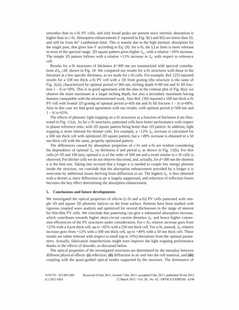
smoother than in c-Si PV cells, and only broad peaks are present since intrinsic absorption ishigher than in c-Si. Absorption enhancements F reported in Fig. 9(c) and 9(f) are lower than 10,and still far from 4n2 Lambertian limit. This is mainly due to the high intrinsic absorption forthe single pass, that gives low F according to Eq. (9): for a-Si, the LLα limit is more relevantin most of the spectral range. 2D square pattern gives higher Jsc, with a relative +20% increase.The simple 1D pattern follows with a relative +11% increase in Jsc with respect to referencecell.
Results for a-Si structures of thickness d=300 nm are summarized with spectral contribu-tions dJsc/dE shown in Fig. 10. We compared our results for a-Si structures with those in theliterature at a few specific thickness, as we made for c-Si cells. For example, Ref. [25] reportedresults for a 338 nm thick a-Si PV cell with a 1D front grating (the structure is the same ofFig. 2(a)), characterized by optimal period a=360 nm, etching depth h=80 nm and Si fill frac-tion 1−b/a=58%. This is in good agreement with the data in the contour plot of Fig. 8(a): weobserve the main maximum at a larger etching depth, but also a secondary maximum havingfeatures compatible with the aforementioned work. Also Ref. [30] reported a 100 nm thick a-SiPV cell with frontal 1D grating of optimal period a=450 nm and Si fill fraction 1−b/a=68%.Also in this case we find good agreement with our results, with optimal period a=500 nm and1−b/a=65%.
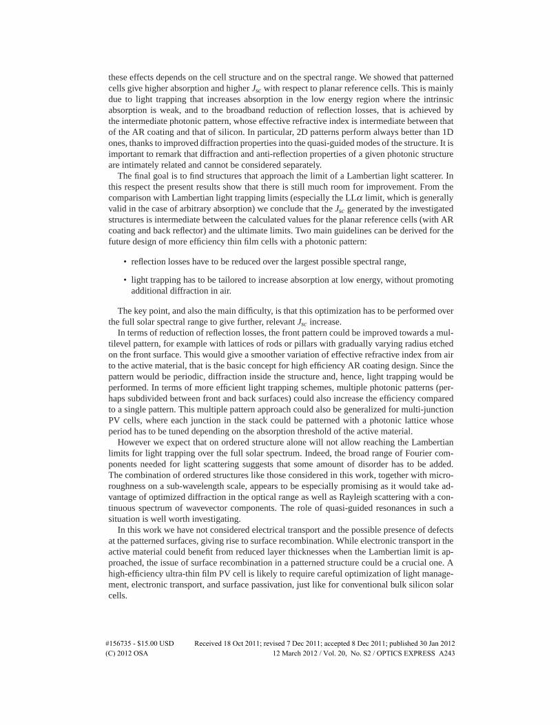
The effects of photonic light trapping on a-Si structures as a function of thickness d are illus-trated in Fig. 11(a). As for c-Si structures, patterned cells have better performance with respectto planar reference ones, with 2D square pattern being better than 1D pattern. In addition, lighttrapping is more relevant for thinner cells. For example, a +12% Jsc increase is calculated fora 500 nm thick cell with optimized 2D square pattern, but a +49% increase is obtained in a 50nm thick cell with the same, properly optimized pattern.
The differences caused by absorption properties of c-Si and a-Si are evident consideringthe dependence of optimal Jsc on thickness d and period a, as shown in Fig. 11(b). For thincells (d=50 and 100 nm), optimal a is of the order of 500 nm and a trend similar to c-Si cells isobserved. For thicker cells we do not observe this trend, and, actually, for d=300 nm the shortesta is the best one. Taking into account that a longer a is needed to couple low energy photonsinside the structure, we conclude that the absorption enhancement provided by a longer a isovercome by additional losses deriving from diffraction in air. The highest Jsc is thus obtainedwith a shorter a, since diffraction in air is largely suppressed, and reduction of reflection lossesbecomes the key effect determining the absorption enhancement.
5. Conclusions and future developments
We investigated the optical properties of silicon (c-Si and a-Si) PV cells patterned with sim-ple 1D and square 2D photonic lattices on the front surface. Patterns have been studied withrigorous coupled wave analysis and optimized for several thicknesses in the range of interestfor thin-film PV cells. We conclude that patterning can give a substantial absorption increase,which contributes towards higher short-circuit current densities Jsc and hence higher conver-sion efficiencies of the PV structures under consideration. For c-Si, relative increase goes from+23% with a 4 μm thick cell, up to +82% with a 250 nm thick cell. For a-Si, instead, Jsc relativeincrease goes from +12% with a 500 nm thick cell, up to +49% with a 50 nm thick cell. Theseresults are rather tolerant with respect to small (up to 10%) deviations from the optimal param-eters. Actually, fabrication imperfections might even improve the light trapping performancethanks to the effects of disorder, as discussed below.
The optical properties of the investigated structures are determined by the interplay betweendifferent physical effects: (i) reflection, (ii) diffraction in air and into the cell material, and (iii)coupling with the quasi-guided optical modes supported by the structure. The dominance of
#156735 - $15.00 USD Received 18 Oct 2011; revised 7 Dec 2011; accepted 8 Dec 2011; published 30 Jan 2012(C) 2012 OSA 12 March 2012 / Vol. 20, No. S2 / OPTICS EXPRESS A240
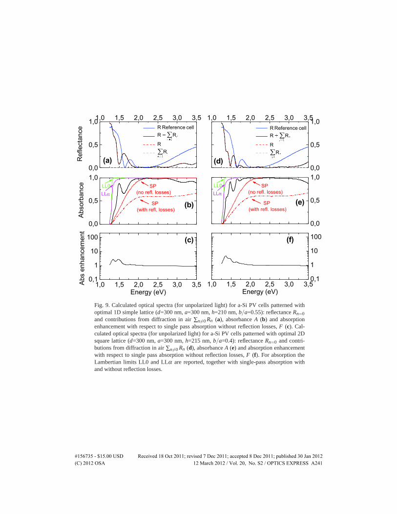
Fig. 9. Calculated optical spectra (for unpolarized light) for a-Si PV cells patterned withoptimal 1D simple lattice (d=300 nm, a=300 nm, h=210 nm, b/a=0.55): reflectance Rn=0and contributions from diffraction in air ∑n�=0 Rn (a), absorbance A (b) and absorptionenhancement with respect to single pass absorption without reflection losses, F (c). Cal-culated optical spectra (for unpolarized light) for a-Si PV cells patterned with optimal 2Dsquare lattice (d=300 nm, a=300 nm, h=215 nm, b/a=0.4): reflectance Rn=0 and contri-butions from diffraction in air ∑n�=0 Rn (d), absorbance A (e) and absorption enhancementwith respect to single pass absorption without reflection losses, F (f). For absorption theLambertian limits LL0 and LLα are reported, together with single-pass absorption withand without reflection losses.
#156735 - $15.00 USD Received 18 Oct 2011; revised 7 Dec 2011; accepted 8 Dec 2011; published 30 Jan 2012(C) 2012 OSA 12 March 2012 / Vol. 20, No. S2 / OPTICS EXPRESS A241
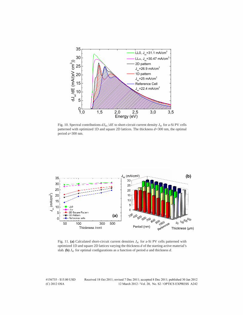
Fig. 10. Spectral contributions dJsc/dE to short-circuit current density Jsc for a-Si PV cellspatterned with optimized 1D and square 2D lattices. The thickness d=300 nm, the optimalperiod a=300 nm.
Fig. 11. (a) Calculated short-circuit current densities Jsc for a-Si PV cells patterned withoptimized 1D and square 2D lattices varying the thickness d of the starting active material’sslab. (b) Jsc for optimal configurations as a function of period a and thickness d.
#156735 - $15.00 USD Received 18 Oct 2011; revised 7 Dec 2011; accepted 8 Dec 2011; published 30 Jan 2012(C) 2012 OSA 12 March 2012 / Vol. 20, No. S2 / OPTICS EXPRESS A242
these effects depends on the cell structure and on the spectral range. We showed that patternedcells give higher absorption and higher Jsc with respect to planar reference cells. This is mainlydue to light trapping that increases absorption in the low energy region where the intrinsicabsorption is weak, and to the broadband reduction of reflection losses, that is achieved bythe intermediate photonic pattern, whose effective refractive index is intermediate between thatof the AR coating and that of silicon. In particular, 2D patterns perform always better than 1Dones, thanks to improved diffraction properties into the quasi-guided modes of the structure. It isimportant to remark that diffraction and anti-reflection properties of a given photonic structureare intimately related and cannot be considered separately.
The final goal is to find structures that approach the limit of a Lambertian light scatterer. Inthis respect the present results show that there is still much room for improvement. From thecomparison with Lambertian light trapping limits (especially the LLα limit, which is generallyvalid in the case of arbitrary absorption) we conclude that the Jsc generated by the investigatedstructures is intermediate between the calculated values for the planar reference cells (with ARcoating and back reflector) and the ultimate limits. Two main guidelines can be derived for thefuture design of more efficiency thin film cells with a photonic pattern:
• reflection losses have to be reduced over the largest possible spectral range,
• light trapping has to be tailored to increase absorption at low energy, without promotingadditional diffraction in air.
The key point, and also the main difficulty, is that this optimization has to be performed overthe full solar spectral range to give further, relevant Jsc increase.
In terms of reduction of reflection losses, the front pattern could be improved towards a mul-tilevel pattern, for example with lattices of rods or pillars with gradually varying radius etchedon the front surface. This would give a smoother variation of effective refractive index from airto the active material, that is the basic concept for high efficiency AR coating design. Since thepattern would be periodic, diffraction inside the structure and, hence, light trapping would beperformed. In terms of more efficient light trapping schemes, multiple photonic patterns (per-haps subdivided between front and back surfaces) could also increase the efficiency comparedto a single pattern. This multiple pattern approach could also be generalized for multi-junctionPV cells, where each junction in the stack could be patterned with a photonic lattice whoseperiod has to be tuned depending on the absorption threshold of the active material.
However we expect that on ordered structure alone will not allow reaching the Lambertianlimits for light trapping over the full solar spectrum. Indeed, the broad range of Fourier com-ponents needed for light scattering suggests that some amount of disorder has to be added.The combination of ordered structures like those considered in this work, together with micro-roughness on a sub-wavelength scale, appears to be especially promising as it would take ad-vantage of optimized diffraction in the optical range as well as Rayleigh scattering with a con-tinuous spectrum of wavevector components. The role of quasi-guided resonances in such asituation is well worth investigating.
In this work we have not considered electrical transport and the possible presence of defectsat the patterned surfaces, giving rise to surface recombination. While electronic transport in theactive material could benefit from reduced layer thicknesses when the Lambertian limit is ap-proached, the issue of surface recombination in a patterned structure could be a crucial one. Ahigh-efficiency ultra-thin film PV cell is likely to require careful optimization of light manage-ment, electronic transport, and surface passivation, just like for conventional bulk silicon solarcells.
#156735 - $15.00 USD Received 18 Oct 2011; revised 7 Dec 2011; accepted 8 Dec 2011; published 30 Jan 2012(C) 2012 OSA 12 March 2012 / Vol. 20, No. S2 / OPTICS EXPRESS A243

Acknowledgments
We are grateful to Simone Zanotto for partecipating in the early phase of this work, and to AlexMellor for helpful suggestions. This work was supported by Fondazione Cariplo under project2010-0523 ”Nanophotonics for thin-film photovoltaics”, and by the EU through Marie CurieAction FP7-PEOPLE-2010-ITN project no. 264687 ”PROPHET”.
#156735 - $15.00 USD Received 18 Oct 2011; revised 7 Dec 2011; accepted 8 Dec 2011; published 30 Jan 2012(C) 2012 OSA 12 March 2012 / Vol. 20, No. S2 / OPTICS EXPRESS A244