photovoltaics fundamentals, technology and application
TRANSCRIPT
23
q 2007 by Taylor & Francis Group, LLC
PhotovoltaicsFundamentals,
Technology andApplication
Roger MessengerFlorida Atlantic University
D.Yogi GoswamiUniversity of South Florida
Hari M. UpadhyayaLoughborough University
Takhir M. RazykovUzbek Academy of Sciences
Ayodhya N. TiwariLoughborough University
Roland WinstonUniversity of California
Robert McConnellNational Renewable Energy Laboratory
23.1 Photovoltaics ..................................................................... 23-1
Introduction † The PV Cell † Manufacture of SolarCells † PV Modules and PV Arrays † The Sun
and PV Array Orientation † System Configurations †
PV System Components † PV System Examples †
Latest Developments in PV †
Future Challenges for PV Systems
23.2 Thin-Film PV Technology ............................................. 23-28
Introduction † Thin-Film Silicon † CadmiumTelluride Solar Cells † Cu(In Ga)Se2 Solar Cells †
Environmental Concerns and Cd Issue † Conclusions
23.3 Concentrating PV Technologies .................................... 23-54
Introduction † CPV Market Entry † Future Growth †Energy Payback † The Need for Qualification Standards
Nomenclature ............................................................................... 23-58
Symbols ......................................................................................... 23-58
Acronyms ...................................................................................... 23-59
References...................................................................................... 23-59
23.1 Photovoltaics
Roger Messenger and D. Yogi Goswami
23.1.1 Introduction
Photovoltaic conversion is the direct conversion of sunlight into electricity with no intervening heat
engine. Photovoltaic devices are solid state; therefore, they are rugged and simple in design and require
very little maintenance. Perhaps the biggest advantage of solar photovoltaic devices is that they can be
constructed as standalone systems to give outputs from microwatts to megawatts. That is why they have
been used as the power sources for calculators, watches, water pumps, remote buildings, communi-
cations, satellites and space vehicles, and even megawatt-scale power plants. Photovoltaic panels can be
23-1

Year
0
200
400
600
800
1000
1200
1400
1600
1800
82 90 00 04
JapanEU-15USAROW
FIGURE 23.1 Worldwide production of photovoltaic panels. (From Maycock, P. EPIA.)
23-2 Handbook of Energy Efficiency and Renewable Energy
made to form components of building skin, such as roof shingles and wall panels. With such a vast array
of applications, the demand for photovoltaics is increasing every year. In 2003, 750 MWp (peak MW or
MW under peak solar radiation of 1 kW/m2) of photovoltaic panels were sold for the terrestrial markets
and the market is growing at a phenomenal rate of 30% per year worldwide (see Figure 23.1).
In the early days of solar cells in the 1960s and 1970s, more energy was required to produce a cell than
it could ever deliver during its lifetime. Since then, dramatic improvements have taken place in the
efficiencies and manufacturing methods. In 1996, the energy payback periods were reduced to about 2.5
to 5 years, depending on the location of use (Nijs 1997) while panel lifetimes were increased to over 25
years. The costs of photovoltaic panels have come down from about $30 to $3 per peak watt over the last
three decades and are targeted to reduce to around $1 per peak watt in the next ten years. Even the $3/W
costs of solar panels results in system costs of $5–$7/W, which is very high for on-grid applications.
To reduce the costs further, efficiency of PV cells must be increased and the manufacturing costs will
have to be decreased. At present, module efficiencies are as high as 15% (Hamakawa 2005). The main
constraint on the efficiency of a solar cell is related to the bandgap of the semiconductor material of a PV
cell. As explained later in this chapter, a photon of light with energy equal to or greater than the bandgap
of the material is able to free-up one electron when absorbed into the material. However, the photons that
have energy less than the bandgap are not useful for this process. When absorbed on the cell, they just
produce heat. And for the photons with more energy than the bandgap, the excess energy above the
bandgap is not useful in generating electricity. The excess energy simply heats up the cell. These reasons
account for a theoretical maximum limit on the efficiency of a conventional single-junction PV cell to less
than 25%. The actual efficiency is even lower because of reflection of light from the cell surface, shading
of the cell due to current collecting contacts, internal resistance of the cell, and recombination of
electrons and holes before they are able to contribute to the current.
The limits imposed on solar cells due to bandgap can be partially overcome by using multiple layers of
solar cells stacked on top of each other, each layer with a bandgap higher than the layer below it. For example
(Figure 23.2), if the top layer is made from a cell of material A (bandgap corresponding to lA), solar
radiation with wavelengths less than lA would be absorbed to give an output equal to the hatched area A.
The solar radiation with wavelength greater than lA would pass through A and be converted to give an
output equal to the hatched area B. The total output and therefore the efficiency of this tandem cell would
be higher than the output and the efficiency of each single cell individually. The efficiency of a
multijunction cell can be about 50% higher than a corresponding single cell. The efficiency would
increase with the number of layers. For this concept to work, each layer must be as thin as possible, which
puts a very difficult if not an insurmountable constraint on crystalline and polycrystalline cells to be made
q 2007 by Taylor & Francis Group, LLC

Wavelength λ
Inte
nsity
W /
m2
λB
A
B
FIGURE 23.2 Energy Conversion from a two layered stacked PV cell. (From Goswami, D. Y., Kreith, F. and Kreider,
J. F. Principles of Solar Engineering, 2nd Ed., Taylor & Francis, Philadelphia, PA, 2000.)
Photovoltaics Fundamentals, Technology and Application 23-3
multijunction. As a result, this concept is being investigated mainly for thin-film amorphous or
microcrystalline solar cells. Efficiencies as high as 24.7% have been reported in the literature (Hamakawa
2005).
In this section, the physics of PV electrical generation will be briefly reviewed, followed by a
discussion of the PV system design process. Several PV system examples will be presented, then a few of
the latest developments in crystalline silicon PV will be summarized, and, finally, some of the present
challenges (2004–2005) facing the large-scale deployment of PV energy sources will be explored.
Emphasis will be on nonconcentrating, crystalline or multicrystalline silicon, terrestrial PV systems
because such systems represent nearly 95% of systems currently being designed and built. However, the
design procedures outlined at the end of the section also can be applied to other PV technologies, such
as thin-films. Thin-film solar cells and concentrating PV cells are described in sections 23.2 and 23.3
respectively.
23.1.2 The PV Cell
23.1.2.1 The p–n Junction
PV cells have been made with silicon (Si), gallium arsenide (GaAs), copper indium diselenide (CIS),
cadmium telluride (CdTe), and a few other materials. The common denominator of PV cells is that a p–n
junction, or the equivalent, such as a Schottky junction, is needed to enable the photovoltaic effect.
Understanding the p–n junction is thus at the heart of understanding how a PV cell converts sunlight into
electricity. Figure 23.3 shows a Si p–n junction.
The junction consists of a layer of n-type Si joined to a layer of p-type Si, with an uninterrupted Si
crystal structure across the junction. The n-layer has an abundance of free electrons and the p-layer has an
abundance of free holes. Under thermal equilibrium conditions, meaning that temperature is the only
external variable influencing the populations of free holes and electrons, the relationship between hole
density, p, and electron density, n, at any given point in the material, is given by
np Z n2i ; ð23:1Þ
where ni is approximately the density of electrons or holes in intrinsic (impurity-free) material. When
impurities are present, then nyNd and pyNa, where Nd and Na are the densities of donor and acceptor
impurities. For Si, niy 1.5!1010 cmK3 at TZ300 K, while Nd and Na can be as large as 1021 cmK3.
Hence, for example, if NdZ1018 on the n-side of the junction, then pZ2.25!102 cmK3.
q 2007 by Taylor & Francis Group, LLC

Holes diffuse
Holes drift
Negative acceptor ions
Space charge layer withtotal number of positiveions = total number ofnegative ions.
left behind at junction
Positive donor ions leftbehind at junction
Electrons drift
Ebuilt-in
P N
Electrons diffuse
FIGURE 23.3 The p–n junction showing electron and hole drift and diffusion. (From Messenger, R. and Ventre, G.
Photovoltaic Systems Engineering, 2nd Ed., CRC Press, Boca Raton, FL, 2004.)
23-4 Handbook of Energy Efficiency and Renewable Energy
Both electrons and holes are subject to random diffusion within the Si crystalline structure, so each
tends to diffuse from regions of high concentration to regions of low concentration. The enormous
concentration differences of hole and electron concentrations between the n-side and the p-side of the
junction cause large concentration gradients across the junction. The net result is that the electrons
diffuse across the junction into the p-region and the holes diffuse across the junction into the n-region, as
shown in Figure 23.3.
Before formation of the junction, both sides of the junction are electrically neutral. Each free electron
on the n-side of the junction comes from a neutral electron donor impurity atom, such as arsenic (As),
whereas each free hole on the p-side of the junction comes from a neutral hole donor (acceptor) impurity
atom, such as boron (B). When the negatively charged electron leaves the As atom, the As atom becomes
a positively charged As ion. Similarly, when the positively charged hole leaves the B atom, the B atom
becomes a negatively charged B ion. Thus, as electrons diffuse to the p-side of the junction, they leave
behind positively charged electron donor ions that are covalently bound to the Si lattice. As holes diffuse
to the n-side of the junction, they leave behind negatively charged hole-donor ions that are covalently
bound to the Si lattice on the p-side of the junction. The diffusion of charge carriers across the junction
thus creates an electric field across the junction, directed from the positive ions on the n-side to the
negative ions on the p-side, as shown in Figure 23.3. Gauss’s law requires that electric field lines originate
on positive charges and terminate on negative charges, so the number of positive charges on the n-side
must be equal to the number of negative charges on the p-side.
Electric fields exert forces on charged particles according to the familiar fZqE relationship. This
force causes the charge carriers to drift. In the case of the positively charged holes, they drift in the
direction of the electric field, i.e., from the n-side to the p-side of the junction. The negatively charged
electrons drift in the direction opposite the field, i.e., from the p-side to the n-side of the junction. If no
external forces are present other than temperature, then the flows of holes are equal in both directions
and the flows of electrons are equal in both directions, resulting in zero net flow of either holes or
electrons across the junction. This is called the law of detailed balance, which is consistent with
Kirchoff ’s current law.
Carrying out an analysis of electron and hole flow across the junction ultimately leads to the
development of the familiar diode equation,
I Z Io eqVkT K1
� �; ð23:2Þ
where q is the electronic charge, k is the Boltzmann constant, T is the junction temperature in K, and V is
the externally applied voltage across the junction from the p-side to the n-side of the junction.
q 2007 by Taylor & Francis Group, LLC

Photovoltaics Fundamentals, Technology and Application 23-5
23.1.2.2 The Illuminated p–n Junction
Figure 23.4 illustrates the effect of photons impinging upon the junction area.
The energy of a photon is given by Equation 23.3:
e Z hn Zhc
l; ð23:3Þ
where l is the wavelength of the photon, h is Planck’s constant (6.625!10K34 J$s), and c is the speed of
light (3!108 m/s).
The energy of a photon in electron-volts (eV) becomes 1.24/l, if l is in mm (1 eV Z1.6!10K19 J). If a
photon has an energy that equals or exceeds the semiconductor bandgap energy of the p-n junction
material, then it is capable of creating an electron-hole pair (EHP). For Si, the bandgap is 1.1 eV, so if the
photon wavelength is less than 1.13 mm, which is in the near infrared region, then the photon will have
sufficient energy to generate an EHP.
Although photons with energies higher than the bandgap energy can be absorbed, one photon can
create only one EHP. The excess energy of the photon is wasted as heat. As photons enter a material, the
intensity of the beam depends upon a wavelength-dependent absorption constant, a. The intensity of the
photon beam as a function of penetration depth into the material is given by F(x)ZFoeKax, where x is
the depth of penetration into the material. Optimization of photon capture, thus, suggests that the
junction should be within (1/a) of the surface to ensure transmission of photons to within a diffusion
length of the p–n junction, as shown in Figure 23.4.
If an EHP is created within one minority carrier diffusion length, Dx, of the junction, then, on the
average, the EHP will contribute to current flow in an external circuit. The diffusion length is defined to
be Lx ZffiffiffiffiffiffiffiffiffiffiDxtx
p, where Dx and tx are the minority carrier diffusion length and lifetime for electrons in the
p-region if xZn, and Dx and tx are the minority carrier diffusion length and lifetime for holes in the
n-region if xZp. So the idea is to quickly move the electron and hole of the EHP to the junction before
either has a chance to recombine with a majority charge carrier. In Figure 23.4, points A, B, and C
represent EHP generation within a minority carrier diffusion length of the junction. But if an EHP is
generated at point D, it is highly unlikely that the electron will diffuse to the junction before
it recombines.
The amount of photon-induced current flowing across the junction and into an external circuit is
directly proportional to the intensity of the photon source. Note that the EHPs are swept across the
junction by the builtin E-field, so the holes move to the p-side and continue to diffuse toward the p-side
external contact. Similarly, the electrons move to the n-side and continue to diffuse to the n-side external
contact. Upon reaching their respective contacts, each contributes to external current flow if an external
I
Junction
EHP
EHP
EHP
Neutral p-region
Neutral n-region_
_ _
++ +
**
EHP
1/α hν
hνhν
hν
A
BC
D*
Ebuilt-in
*
FIGURE 23.4 The illuminated p–n junction showing desirable geometry and the creation of electron-hole pairs.
(From Messenger, R. and Ventre, G. Photovoltaic Systems Engineering, 2nd Ed., CRC Press, Boca Raton, FL, 2004.)
q 2007 by Taylor & Francis Group, LLC

23-6 Handbook of Energy Efficiency and Renewable Energy
path exists. In the case of holes, they must recombine at the contact with an electron that enters the
material at the contact. Electrons, on the other hand, are perfectly happy to continue flowing through an
external copper wire.
At this point, an important observation can be made. The external voltage across the diode that results
in significant current flow when no photons are present, is positive from p to n. The diode current and
voltage are defined in this direction, and the diode thus is defined according to the passive sign
convention. In other words, when no photons impinge on the junction, the diode dissipates power. But
when photons are present, the photon-induced current flows opposite to the passive direction. Therefore,
current leaves the positive terminal, which means that the device is generating power. This is the
photovoltaic effect. The challenge to the manufacturers of PV cells is to maximize the capture of photons
and, in turn, maximize the flow of current in the cell for a given incident photon intensity. Optimization
of the process is discussed in detail in Messenger and Ventre (2004). When the photocurrent is
incorporated into the diode equation, the result is
I Z Il KIo eqVkT K1
� �yIl KIoe
qVkT : ð23:4Þ
Note that in Equation 23.4, the direction of the current has been reversed with respect to the cell voltage.
With the active sign convention implied by Equation 23.4, the junction device is now being defined as a
cell, or PV cell. Figure 23.5 shows the I–V curves for an ideal PV cell and a typical PV cell, assuming the
cell has an area of approximately 195 cm2.
It is evident that the ideal curve closely represents that of an ideal current source for cell voltages below
0.5 V, and it closely represents that of an ideal voltage source for voltages near 0.6 V. The intersection of
the curve with the VZ0 axis represents the short circuit current of the cell. The intersection of the curve
with the IZ0 axis represents the open circuit voltage of the cell. To determine the open circuit voltage of
the cell, simply set IZ0 and solve Equation 23.4 for VOC. The result is
Voc ZkT
qln
Il
IO
: ð23:5Þ
The direct dependence of I on Il and the logarithmic dependence of VOC on Il is evident from Equation
23.4 and Equation 23.5, as well as from Figure 23.5.
0
2
0 0.1 0.2 0.3 0.4 0.5 0.6 0.7
Cel
l cur
rent
, A
Cell voltage, V
1 kW/ m2
750 W/ m2
500 W/ m2
250 W/ m2
Real cell
4
6
CellI+
_V
FIGURE 23.5 I–V characteristics of real and ideal PV cells under different illumination levels. (From Messenger, R.
and Ventre, G. Photovoltaic Systems Engineering, 2nd Ed., CRC Press, Boca Raton, FL, 2004.)
q 2007 by Taylor & Francis Group, LLC

0
1
2
3
Cel
l pow
er, W
0 0.2 0.4 0.6
Cell voltage,V
FIGURE 23.6 Power vs. voltage for a PV cell for four illumination levels. (From Messenger, R. and Ventre, G.
Photovoltaic Systems Engineering, 2nd Ed., CRC Press, Boca Raton, FL, 2004.)
Photovoltaics Fundamentals, Technology and Application 23-7
The departure of the real curve from the ideal prediction is primarily due to unavoidable series
resistance between the cell contacts and the junction.
23.1.2.3 Properties of the PV Cell
Another property of the I–V curves of Figure 23.5 is the presence of a single point on each curve at which
the power delivered by the cell is a maximum. This point is called the maximum power point of the cell,
and is more evident when cell power is plotted vs. cell voltage, as shown in Figure 23.6. Note that the
maximum power point of the cell remains at a nearly constant voltage as the illumination level of the
cell changes.
Not shown in Figure 23.5 or Figure 23.6 is the temperature dependence of the photocurrent. It turns
out that Io increases rapidly with temperature. Thus, despite the KT/q multiplying factor, the maximum
available power from a Si PV cell decreases at approximately 0.47%/8C, as shown in Figure 23.7.
Furthermore, the maximum power voltage also decreases by approximately this same factor. An
increase of 258C is not unusual for an array of PV cells, which corresponds to a decrease of approximately
12% in maximum power and in maximum power voltage. Because of this temperature degradation of the
performance of a PV cell, it is important during the system design phase to endeavor to keep the PV cells
as cool as possible.
50°C
0°C
−25°C
25°C
1
2
3
4
00
0.2 0.4 0.6
Cell voltage, V
Cel
l pow
er, W
FIGURE 23.7 Temperature dependence of the power vs. voltage curve for a PV cell. (From Messenger, R. and
Ventre, G. Photovoltaic Systems Engineering, 2nd Ed., CRC Press, Boca Raton, FL, 2004.)
q 2007 by Taylor & Francis Group, LLC

23-8 Handbook of Energy Efficiency and Renewable Energy
23.1.3 Manufacture of Solar Cells
23.1.3.1 Manufacture of Crystalline and Multicrystalline Silicon PV Cells
Although crystalline and multicrystalline silicon PV cells require highly purified, electronic-grade silicon,
the material can be about an order of magnitude less pure than semiconductor grade silicon and still yield
relatively high performance PV cells. Recycled or rejected semiconductor-grade silicon is often used as
the feedstock for PV-grade silicon. Once adequately refined silicon is available, a number of methods
have been devised for the production of single-crystal and multicrystalline PV cells. Single-crystal Si PV
cells have been fabricated with conversion efficiencies just over 20%, while conversion efficiencies of
champion multicrystalline Si PV cells are about 16% (Hanoka 2002; Rosenblum et al. 2002).
Single-crystal Si cells are almost exclusively fabricated from large single crystal ingots of Si that are
pulled from molten, PV-grade Si. These ingots, normally p-type, are typically on the order of 200 mm in
diameter and up to 2 m in length. The Czochralski method (Figure 23.8a) is the most common method
of growing single-crystal ingots.
A seed crystal is dipped in molten silicon doped with a p-material (boron) and drawn upward under
tightly controlled conditions of linear and rotational speed and temperature. This process produces
cylindrical ingots of typically 10-cm diameter, although ingots of 20-cm diameter and more than 1 m
long can be produced for other applications. An alternative method is called the float zone method
(Figure 23.8b). In this method a polycrystalline ingot is placed on top of a seed crystal and the interface is
melted by a heating coil around it. The ingot is moved linearly and rotationally, under controlled
conditions. This process has the potential to reduce the cell cost. Figure 23.9 illustrates the process of
manufacturing a cell from an ingot.
The ingots are sliced into wafers that are approximately 0.25 mm thick. The wafers are further
trimmed to a nearly square shape, with only a small amount of rounding at the corners. Surface
degradation from the slicing process is reduced by chemically etching the wafers. To enhance photon
absorption, it is common practice to use a preferential etching process to produce a textured surface
finish. An n-layer is then diffused into the wafer to produce a p–n junction, contacts are attached, and the
cell is then encapsulated into a module (Figure 23.10).
Detailed accounts of cell and module fabrication processes can be found in Hanoka (2002); Messenger
and Ventre (2004); Hamakawa (2005), and Saitoh (2005).
Growing and slicing single-crystal Si ingots is highly energy intensive, and, as a result, imposes a
relatively high energy cost on this method of cell fabrication. This high-energy cost imposes a lower limit
on the cost of production of a cell and, although the cell will ultimately generate more energy than was
used to produce it, the energy payback time is longer than desirable. Reducing the energy cost of cell and
module fabrication has been the subject of a great deal of research over the past 40 years. The high-energy
cost of crystalline Si led to the work on thin-films of amorphous Si, CdTe, and other materials that is
Seed
Crystal
Molten silicon
Czochralski method(a)
PolycrystallineSilicon
Molten zone
Movable heater winding
Single crystal seed
Float zone method(b)
FIGURE 23.8 Crystalline silicon ingot production methods. (From Goswami, D. Y., Kreith, F. and Kreider, J. F.
Principles of Solar Engineering, 2nd Ed., Taylor & Francis, Philadelphia, PA, 2000.)
q 2007 by Taylor & Francis Group, LLC

Molten solargrade silicondoped withboron
Crystalline orpolycrystal ingots
Wafer slicingPolishing
and lappingwafers
Doping withphosphorous
Reposition ofelectricalcontacts
AR Coatingencapsulation
Modules
FIGURE 23.9 Series of processes for the manufacture of crystalline and polycrystalline cells. (From Goswami, D. Y.,
Kreith, F. and Kreider, J. F. Principles of Solar Engineering, 2nd Ed., Taylor & Francis, Philadelphia, PA, 2000.)
Photovoltaics Fundamentals, Technology and Application 23-9
described later in this handbook. A great deal of work has also gone into developing methods of growing
Si in a manner that will result in lower-energy fabrication costs.
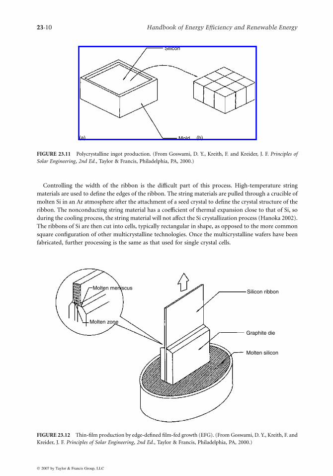
Three methods that are less energy intensive are now commonly in use—crucible growth, the EFG
process, and string ribbon technology. These methods, however, result in the growth of multicrystalline
Si, which, upon inspection, depending upon the fabrication process, has a speckled surface appearance,
as opposed to the uniform color of single crystal Si. Multicrystalline Si has electrical and thermodynamic
characteristics that match single crystal Si relatively closely, as previously noted.
The crucible growth method involves pouring molten Si into a quartz crucible and carefully
controlling the cooling rate (Figure 23.11).
A seed crystal is not used, so the resulting material consists of a collection of zones of single crystals
with an overall square cross-section. It is still necessary to saw the ingots into wafers, but the result is
square wafers rather than round wafers that would require additional sawing and corresponding loss of
material. Wafers produced by this method can achieve conversion efficiencies of 15% or more
(Hamakawa 2005).
The edge-defined film-fed growth (EFG) process is another method currently being used to produce
commercial cells (ASE International). The process involves pulling an octagon tube, 6-m long, with a wall
thickness of 330 mm, directly from the Si melt. The octagon is then cut by a laser along the octagonal
edges into individual cells. Cell efficiencies of 14% have been reported for this fabrication method
(Rosenblum et al. 2002). Figure 23.12 illustrates the process.
A third method of fabrication of multicrystalline Si cells involves pulling a ribbon of Si, or dendritic
web, from the melt (Figure 23.13).
FIGURE 23.10 Assembly of solar cells to form a module. (From Goswami, D. Y., Kreith, F. and Kreider, J. F.
Principles of Solar Engineering, 2nd Ed., Taylor & Francis, Philadelphia, PA, 2000.)
q 2007 by Taylor & Francis Group, LLC
Silicon
Mold(a) (b)
FIGURE 23.11 Polycrystalline ingot production. (From Goswami, D. Y., Kreith, F. and Kreider, J. F. Principles of
Solar Engineering, 2nd Ed., Taylor & Francis, Philadelphia, PA, 2000.)
23-10 Handbook of Energy Efficiency and Renewable Energy
Controlling the width of the ribbon is the difficult part of this process. High-temperature string
materials are used to define the edges of the ribbon. The string materials are pulled through a crucible of
molten Si in an Ar atmosphere after the attachment of a seed crystal to define the crystal structure of the
ribbon. The nonconducting string material has a coefficient of thermal expansion close to that of Si, so
during the cooling process, the string material will not affect the Si crystallization process (Hanoka 2002).
The ribbons of Si are then cut into cells, typically rectangular in shape, as opposed to the more common
square configuration of other multicrystalline technologies. Once the multicrystalline wafers have been
fabricated, further processing is the same as that used for single crystal cells.
Silicon ribbon
Graphite die
Molten silicon
Molten zone
Molten meniscus
FIGURE 23.12 Thin-film production by edge-defined film-fed growth (EFG). (From Goswami, D. Y., Kreith, F. and
Kreider, J. F. Principles of Solar Engineering, 2nd Ed., Taylor & Francis, Philadelphia, PA, 2000.)
q 2007 by Taylor & Francis Group, LLC

Web crystal
Supporting dendrite
Molten silicon
FIGURE 23.13 Thin-film production by dendritic web growth. (From Goswami, D. Y., Kreith, F. and Kreider, J. F.
Principles of Solar Engineering, 2nd Ed., Taylor & Francis, Philadelphia, PA, 2000.)
Photovoltaics Fundamentals, Technology and Application 23-11
23.1.3.2 Amorphous Silicon and Multijunction-Thin-Film Fabrication
Amorphous silicon (a-Si) cells are made as thin-films of a-Si:H alloy doped with phosphorous and boron
to make n and p layers respectively. The atomic structure of an a-Si cell does not have any preferred
orientation. The cells are manufactured by depositing a thin layer of a-Si on a substrate (glass, metal or
plastic) from glow discharge, sputtering or chemical vapor deposition (CVD) methods. The most
common method is by an RF glow discharge decomposition of silane (SiH4) on a substrate heated to a
temperature of 200–3008C. To produce p-silicon, diborane (B2H6) vapor is introduced with the silane
vapor. Similarly phosphene (PH3) is used to produce n-silicon. The cell consists of an n-layer, and
intermediate undoped a-Si layer, and a p-layer on a substrate. The cell thickness is about 1 mm. The
manufacturing process can be automated to produce rolls of solar cells from rolls of substrate.
Figure 23.14 shows an example of roll-to-roll a-Si cell manufacturing equipment using a plasma CVD
method. This machine can be used to make multijunction or tandem cells by introducing the appropriate
materials at different points in the machine.
The four previously mentioned cell fabrication techniques require contacts on the front surface and on
the back surface of the cells. Front-surface contacts need to cover enough area to minimize series
resistance between cell and contact, but if too much area is covered, then photons are blocked from
entering the crystal. Thus, it is desirable, if possible, to design cells such that both contacts are on the back
of the cell. Green and his PV team at the University of South Wales have devised a buried contact cell
(Green and Wenham 1994) that has both contacts on the back and also is much thinner and therefore
much less material-intensive than conventional Si cells. In conventional cells, charge carrier flow is
perpendicular to the cell surface, while in the buried contact cell, even though the multiple p–n junctions
are parallel to the cell surfaces, charge carrier flow is parallel to the cell surfaces. The fabrication process
involves depositing alternate p-type and n-type Si layers, each about 1-mm thick, on an insulating
substrate or superstrate. Grooves are laser cut in the layers and contacts are deposited in the grooves.
Elimination of the ingot and wafer steps in processing, along with the reduced amount of material used,
reduces correspondingly the energy overhead of cell production. Conversion efficiencies in excess of 20%
and high cell fill factors have been achieved with this technology.
q 2007 by Taylor & Francis Group, LLC

Pay−off P
Gas gateStainless steel
(anode)
I N P I N Take − Up
Plasma
CathodeRF Generator13.56 MHz
Vacuumpump
FIGURE 23.14 A schematic diagram of a roll-to-roll plasma CVD machine. (Adapted from ASE International,
http://www.ase-international.com)
23-12 Handbook of Energy Efficiency and Renewable Energy
23.1.4 PV Modules and PV Arrays
Because individual cells have output voltages limited to approximately 0.5 V and output currents limited
to approximately 7 A, it is necessary to combine cells in series and parallel to obtain higher voltages and
currents. A typical PV module consists of 36 cells connected in series in order to produce a maximum
power voltage of approximately 17 V, with a maximum power current of approximately 7 A at a
temperature of 258C. Such a module will typically have a surface area of about 10 ft2. Modules also exist
with 48 or more series cells so that three modules in series will produce the same output voltage and
current as four 36-cell modules in series. Other larger modules combine cells in series and in parallel to
produce powers up to 300 W per module.
Modules must be fabricated so the PV cells and interconnects are protected from moisture and are
resistant to degradation from the ultraviolet component of sunlight. Since the modules can be expected
to be exposed to a wide range of temperatures, they must be designed so that thermal stresses will not
cause delamination. Modules must also be resistant to blowing sand, salt, hailstones, acid rain and other
unfriendly environmental conditions. And, of course, the module must be electrically safe over the long
term. A typical module can withstand a pressure of 50 psf and large hailstones and is warranteed for 25
years. Details on module fabrication can be found in Messenger and Ventre (2004); Saitoh (2005), and
Bohland (1998).
It is important to realize that when PV cells with a given efficiency are incorporated into a PV module,
the module efficiency will be less than the cell efficiency, unless the cells are exactly identical electrically.
When cells are operated at their maximum power point, this point is located on the cell I–V curve at the
point where the cell undergoes a transition from a nearly ideal current source to a nearly ideal voltage
source. If the cell I–V curves are not identical, since the current in a series combination of cells is the same
in each cell, each cell of the combination will not necessarily operate at its maximum power point.
Instead, the cells operate at a current consistent with the rest of the cells in the module, which may not be
the maximum power current of each cell.
When modules are combined to further increase system voltage and/or current, the collection of
modules is called an array. For the same reason that the efficiency of a module is less than the efficiencies
of the cells in the module, the efficiency of an array is less than the efficiency of the modules in the array.
However, because a large array can be built with subarrays that can operate essentially independently of
each other, in spite of the decrease in efficiency at the array level, PV arrays that produce in excess of
1 MW are in operation at acceptable efficiency levels. The bottom line is that most efficient operation is
achieved if modules are made of identical cells and if arrays consist of identical modules.
q 2007 by Taylor & Francis Group, LLC

23.1.5 The Sun and PV Array Orientation
As explained in detail in Chapter 19, total solar radiation is composed of components, direct or beam,
diffuse and reflected. In regions with strong direct components of sunlight, it may be advantageous to
have a PV array mount that will track the sun. Such tracking mounts can improve the daily performance
of a PV array by more than 20% in certain regions. In cloudy regions, tracking is less advantageous.
The position of the sun in the sky can be uniquely described by two angles—the azimuth, g, and the
altitude, a. The azimuth is the deviation from true south. The altitude is the angle of the sun above the
horizon. When the altitude of the sun is 908, the sun is directly overhead.
Another convenient, but redundant, angle, is the hour angle, u. Because the earth rotates 3608 in 24 h,
it rotates 158/h. The sun thus appears to move along its arc 158 toward the west each hour. The hour angle
is 08 at solar noon, when the sun is at its highest point in the sky during a given day. In this handbook, we
have a sign convention such that the hour angle and the solar azimuth angle are negative before noon and
positive after noon. For example, at 10:00 a.m. solar time, the hour angle will be K308.
A further important angle that is used to predict sun position is the declination, d. The declination is
the apparent position of the sun at solar noon with respect to the equator. When dZ0, the sun appears
overhead at solar noon at the equator. This occurs on the first day of fall and on the first day of spring. On
the first day of northern hemisphere summer (June 21), the sun appears directly overhead at a latitude, L,
of 23.458 north of the equator. On the first day of winter (December 21), the sun appears directly
overhead at a latitude of 23.458 south of the equator. At any other latitude, the altitude, aZ908KjLKdj
when the sun is directly south, (or north) i.e., at solar noon. At solar noon, the sun is directly south for
LOd and directly north for L!d. Note that if L is negative, it refers to the southern hemisphere.
Several important formulas for determining the position of the sun (Messenger and Ventre 2004;
Markvart 1994) include the following, where n is the day of the year with January 1 being day 1:
d Z 23:458sin360½nK80�
365; ð23:6Þ
u ZG158ðhours from local solar noonÞ ð23:7Þ
sin a Z sin d sin L Ccos d cos L cos u; ð23:8Þ
and
cos g Zcos d sin u
cos a: ð23:9Þ
Solution of Equation 23.6 through Equation 23.9 shows that for optimal annual performance of a fixed
PVarray, it should face directly south and should be tilted at an angle approximately equal to the latitude,
L. For best summer performance, the tilt should be at LK158 and for best winter performance, the array
should be tilted at an angle of LC158.
Although Equation 23.6 through Equation 23.9 can be used to predict the location of the sun in the
sky at any time on any day at any location, they cannot be used to predict the degree of cloud cover.
Cloud cover can only be predicted on a statistical basis for any region, and thus the amount of sunlight
available to a collector will also depend upon cloud cover. The measure of available sunlight is the peak
sun hour (psh). If sunlight intensity is measured in kW/m2, then if the sunlight intensity is integrated
from sunrise to sunset over 1 m2 of surface, the result will be measured in kWh. If the daily kWh/m2 is
divided by the peak sun intensity, which is defined as 1 kW/m2, the resulting units are hours. Note that
this hour figure multiplied by 1 kW/m2 results in the daily kWh/m2. Hence, the term peak sun hours,
because the psh is the number of hours the sun would need to shine at peak intensity to produce the
Photovoltaics Fundamentals, Technology and Application 23-13
q 2007 by Taylor & Francis Group, LLC

23-14 Handbook of Energy Efficiency and Renewable Energy
daily sunrise to sunset kWh. Obviously the psh is also equivalent to kWh/m2/day. For locations in the
United States, the National Renewable Energy Laboratory publishes psh for fixed and single-axis
tracking PV arrays at tilts of horizontal, latitude K158, latitude, latitude C158, and vertical. NREL also
tabulates data for double axis trackers. These tables are extremely useful for determining annual
performance of a PV array.
23.1.6 System Configurations
Figure 23.15 illustrates four possible configurations for PV systems.
Perhaps the simplest system is that of Figure 23.15a, in which the output of the PV module or array is
connected directly to a DC load. This configuration is most commonly used with a fan or a water pump,
although it is likely that the water pump will also use a linear current booster (LCB) between the array
and the pump motor. Operation of the LCB will be explained later.
The configuration of Figure 23.15b includes a charge controller and storage batteries so the PV array
can produce energy during the day that can be used day or night by the load. The charge controller
serves a dual function. If the load does not use all the energy produced by the PV array, the charge
controller prevents the batteries from overcharge. While flooded lead acid batteries require over-
charging about once per month, frequent overcharging shortens the life of the batteries. As the batteries
become discharged, the charge controller disconnects the load to prevent the batteries from over-
discharge. Normally PV systems incorporate deep discharge lead-acid batteries, but the life of these
batteries is reduced significantly if they are discharged more than 80%. Modern charge controllers
typically begin charging as constant current sources. In the case of a PV system, this simply means that
all array current is directed to the batteries. This is called the “bulk” segment of the charge cycle. After
the battery voltage reaches the bulk voltage, which is an owner programmable value, as determined by
the battery type and the battery temperature, the charging cycle switches to a constant voltage mode,
commonly called the absorption mode. During the absorption charge mode, the charge controller
maintains the bulk charge voltage for a preprogrammed time, again depending upon manufacturers’
recommendations. During the absorption charge, battery current decreases as the batteries approach
full charge. At the end of the absorption charge period, the charging voltage is automatically reduced to
the “float” voltage level, where the charging current is reduced to a “trickle” charge. Because quality
charge controllers are microprocessor controlled, they have clock circuitry so that they can be
programmed to automatically subject the batteries to an “equalization” charge approximately once a
month. The equalization mode applies a voltage higher than the bulk voltage for a preset time to
purposely overcharge the batteries. This process causes the electrolyte to bubble, which helps to mix the
electrolyte as well as to clean the battery plates. Equalization is recommended only for flooded lead-acid
batteries. Sealed varieties can be seriously damaged if they are overcharged.
PV Arrayac
loads
AC system with battery backup and fossil generator.
Chargecontroller
Storagebatteries
Inverter
Generator
PV Array Inverter Utilitygrid
Grid connected system.
(c)
(d)
PV Array Load
Direct coupled DC system.
PV Array Load
DC system with battery backup.
Chargecontroller
Storagebatteries
(a)
(b)
FIGURE 23.15 Several examples of PV systems.
q 2007 by Taylor & Francis Group, LLC

Chargingcurrent
Time
Bulk stageAbsorption
stage Float stage
Bulk voltage
Float voltageB
egin
cha
rgin
g
FIGURE 23.16 Charging cycle for typical PV charge controller.
Photovoltaics Fundamentals, Technology and Application 23-15
Figure 23.16 shows the currents and voltages during the bulk, absorption and float parts of the
charging cycle. Note that all settings are programmable by the user in accordance with manufacturers’
recommendations. Some charge controllers incorporate maximum power tracking as a part of their
charge control algorithm. Because the maximum power voltage of a module or an array is generally
higher than needed to charge the batteries, the array will not normally operate at its maximum power
point when it is charging batteries, especially if the array temperature is low. For example, if it takes
14.4 V to charge a 12.6-V battery, and if a module maximum power voltage is 17 V, then the charging
current can be increased by a factor of 17/14.4, or approximately 18%, assuming close to 100% efficiency
of the MPT.
The configuration of Figure 23.15c incorporates an inverter to convert the DC PV array output to AC
and a backup generator to supply energy to the system when the supply from the sun is too low to meet
the needs of the load. Normally the backup generator will be a fossil-fueled generator, but it is also
possible to incorporate wind or other renewable generation into the system. In this case, the charge
controller prevents overcharge of the batteries. The inverter is equipped with voltage sensing circuitry
so that if it detects the battery voltage going too low, it will automatically start the generator so the
generator will provide power for the load as well as provide charging current for the batteries. This
system is called a hybrid system because it incorporates the use of more than one energy source.
The first three configurations are standalone systems. The fourth system, shown in Figure 23.15d, is a
grid-connected, or utility-interactive, system. The inverter of a utility interactive system must meet more
stringent operational requirements than the standalone inverter. The inverter output voltage and current
must be of “utility-grade” quality. This means that it must have minimal harmonic content.
Furthermore, the inverter must sense the utility and, if utility voltage is lost, the inverter must shut
down until utility voltage is restored to within normal limits.
23.1.7 PV System Components
23.1.7.1 Maximum Power Trackers and Linear Current Boosters
The linear current booster (LCB) was mentioned in conjunction with the water pumping example. The
function of the LCB is to match the motor I–V characteristic to the maximum power point of the PV
array, so that at all times the array delivers maximum power to the load. Note that the LCB acts as a
DC-to-DC transformer, converting a higher voltage and lower current to a lower voltage and higher
current, with minimal power loss in the conversion process. A more general term that includes the
q 2007 by Taylor & Francis Group, LLC

Load 2
Load 1
IV=Pm
ax1
IV= P
max2
I
V
s
ss
ss
ss
A
B
C D
Bmax
Amax s
Cmax
Dmax
FIGURE 23.17 Operation of the LCB or MPT. (From Messenger, R. and Ventre, G. Photovoltaic Systems Engineering,
2nd Ed., CRC Press, Boca Raton, FL, 2004.)
23-16 Handbook of Energy Efficiency and Renewable Energy
possibility of converting voltage upward defines the maximum power tracker (MPT). Figure 23.17 shows
the operating principle of the LCB and MPT.
Note that normally the I–V characteristic of the load will not intersect the I–V characteristic of the PV
array at the maximum power point of the array, as shown by points A, B, C, and D for the two loads and
the two sunlight intensity levels. For the lower intensity situation, the characteristic of load 1 intersects
the array characteristic at point C and the characteristic of load 2 intersects the array characteristic at
point A. The two hyperbolas are the loci of points where the IV product is equal to the maximum
available power from the array at the particular sunlight intensity. Hence, the intersection of these
hyperbolas with the load characteristics represents the transfer of all available power from the array to the
load. Although the increase in power for points B and C is not particularly impressive, as shown by points
Bmax and Cmax, the increase in power for points A and D is considerably greater, as shown by points Amax
and Dmax. The assumption here, of course, is 100% efficiency in the transformation. In fact, efficiencies in
excess of 95% are not unusual for quality MPT and LCB devices.
The final observation for Figure 23.17 is that points Amax and Bmax occur at voltages below the
maximum power voltages of the array, while Cmax and Dmax occur at voltages above the maximum power
voltages of the array. Because the input voltage and current of the MPT or LCB is the maximum power
voltage and current of the array, the MPT or LCB output voltage and current points Amax and Bmax
represent down conversion of the array voltage and points Cmax and Dmax represent up conversion of the
array voltage. These forms of conversion are discussed in power electronics books, such as that by Krein
(1998). The difference between the MPT and the LCB is that the LCB only performs a down conversion,
so the operating voltage of the load is always below the maximum power voltage point of the array. The
terms LCB and MPT are often used interchangeably for down conversion, but normally LCB is limited to
the description of the black box that optimizes performance of pumps, whereas MPT is used for more
general applications.
23.1.7.2 Inverters
Inverters convert DC to AC. The simplest inverter converts DC to square waves. Although square waves
will operate many AC loads, their harmonic content is very high, and, as a result, there are many
situations where square waves are not satisfactory. Other more suitable inverter output waveforms
include the quasi-sine wave and the utility-grade sine wave. Both are most commonly created by the use
of multilevel H-bridges controlled by microprocessors. There are three basic configurations for inverters:
standalone, grid-tied, and UPS. The standalone inverter must act as a voltage source that delivers a
prescribed amplitude and frequency rms sine wave without any external synchronization. The grid-tied
inverter is essentially a current source that delivers a sinusoidal current waveform to the grid that is
q 2007 by Taylor & Francis Group, LLC

Photovoltaics Fundamentals, Technology and Application 23-17
synchronized by the grid voltage. Synchronization is typically sufficiently close to maintain a power factor
in excess of 0.9. The UPS inverter combines the features of both the standalone and the grid-tied inverter,
so that if grid power is lost, the unit will act as a standalone inverter while supplying power to emergency
loads. IEEE Standard 929 (IEEE 2000) requires that any inverter that is connected to the grid must
monitor the utility grid voltage, and, if the grid voltage falls outside prescribed limits, the inverter must
stop delivering current to the grid. Underwriters Laboratory (UL) Standard 1741 (UL 1999) provides the
testing needed to ensure compliance with IEEE 929.
Although it may seem to be a simple matter to shut down if the utility shuts down, the matter is
complicated by the possibility that additional utility-interactive PV systems may also be on line. Hence, it
may be possible for one PV system to “fool” another system into thinking that it is really the utility. To
prevent this “islanding” condition, sophisticated inverter control algorithms have been developed to
ensure that an inverter will not appear as the utility to another inverter. Some PV system owners do not
want their PV system to shut down when the utility shuts down. Such a system requires a special inverter
that has two sets of AC terminals. The first set, usually labeled AC IN, is designed for connection to the
utility. If the utility shuts down, this set of terminals disconnects the inverter output from the utility, but
continues to monitor utility voltage until it is restored. When the utility connection is restored, the
inverter will first meet the needs of the emergency loads and then will feed any excess output back to the
main distribution panel.
The second set of terminals is the emergency output. If the utility shuts down, the inverter almost
instantaneously transfers into the emergency mode, in which it draws power from the batteries and/or
the PV array to power the emergency loads. In this system, the emergency loads must be connected to a
separate emergency distribution panel. Under emergency operation, the loads in the main distribution
panel are without power, but the emergency panel remains energized. Such a system is shown in
Figure 23.18.
The reader is referred to the book by Messenger and Ventre (2004) and to that by Krein (1998) for
detailed explanations of the operation of inverters, including the methods used to ensure that utility
interactive inverters meet UL 1741 testing requirements.
23.1.7.3 Balance of System Components (BOS)
Aside from the array, the charge controller, and the inverter, a number of other components are needed in
a code-compliant PV system. For example, if a PV array consists of multiple series-parallel connections,
as shown in Figure 23.19, then it is necessary to incorporate fuses or circuit breakers in series with each
series string of modules, defined as a source circuit.
This fusing is generally accomplished by using a source circuit combiner box as the housing for the
fuses or circuit breakers, as shown in Figure 23.19. The combiner box should be installed in a readily
accessible location. The PV output circuit of Figure 23.19 becomes the input to the charge controller, if a
charge controller is used. If multiple parallel source circuits are used, it may be necessary to use more
than one charge controller, depending upon the rating of the charge controller. When more than one
charge controller is used, source circuits should be combined into separate output circuits for each charge
controller input. In a utility-interactive circuit with no battery backup, a charge controller is not
Inverter
dc in
H
N
H
N
acIn
out Maindistrpanel
Emergencypanel
AB
C
PUC
FIGURE 23.18 Utility-interactive PV system connections to emergency loads and to utility.
q 2007 by Taylor & Francis Group, LLC

Source circuits
Output
circuit
Sourcecircuit
combinerbox
FIGURE 23.19 Example of PV source and output circuits.
23-18 Handbook of Energy Efficiency and Renewable Energy
necessary. The PVoutput circuit connects directly to the inverter through either a DC disconnect or a DC
ground fault detection and interruption device (GFDI).
A GFDI device is required by the National Electrical Code (NEC) (NFPA 2002) whenever a PV array is
installed on a residential rooftop. The purpose of the device is to detect current flow on the grounding
conductor. The grounding conductor is used to ground all metal parts of the system. In a properly
installed and operating system, no current will flow on the grounding conductor. Normally the negative
conductor of the PV array is grounded, but this ground, if properly installed, will be attached to the
grounding conductor at only one point, as shown in Figure 23.20, where the negative PV output
conductor is connected to the equipment grounding bus through the 1A circuit breaker. The 1A circuit
breaker is ganged to the 100 A circuit breaker so that if the current through the 1A circuit breaker
exceeds 1A, both breakers will trip. When the two circuit breakers are open, current flow on both the PV
output circuit conductors as well as the grounding conductor is interrupted. If the fault current on the
grounding conductor was the result of an arcing condition between one of the PV circuit conductors and
ground, the arc will be extinguished, thus preventing a fire from starting.
The NEC also requires properly rated disconnects at the inputs and outputs of all power conditioning
equipment. An additional disconnect will be needed at the output of a charge controller as well as
between any battery bank and inverter input or DC load center. If the disconnect is to disconnect DC,
then the NEC requires that it be rated for DC. Additional disconnects are needed at the output of any
inverter. If the inverter is utility interactive with battery backup for emergency loads, it is desirable to
include an inverter bypass switch at the inverter output in case inverter maintenance is required without
interruption of power to emergency loads. In addition to the inverter bypass switch, many utilities
100 A
1A
PV output Inv or CC input
Equipment
ground
bus
FIGURE 23.20 Use of GFDI.
q 2007 by Taylor & Francis Group, LLC
require a visible, lockable, accessible, load break, disconnect between the inverter output and the point of
utility connection. This switch is for use by the utility if they deem it necessary to disconnect the inverter
from the line for any reason.
The point of utility connection for a utility-interactive system will normally be a backfed circuit breaker
in a distribution panel. This circuit breaker is to be labeled so maintenance workers will recognize it as a
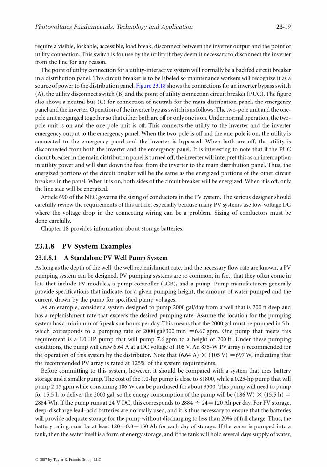
source of power to the distribution panel. Figure 23.18 shows the connections for an inverter bypass switch
(A), the utility disconnect switch (B) and the point of utility connection circuit breaker (PUC). The figure
also shows a neutral bus (C) for connection of neutrals for the main distribution panel, the emergency
panel and the inverter. Operation of the inverter bypass switch is as follows: The two-pole unit and the one-
pole unit are ganged together so that either both are off or only one is on. Under normal operation, the two-
pole unit is on and the one-pole unit is off. This connects the utility to the inverter and the inverter
emergency output to the emergency panel. When the two-pole is off and the one-pole is on, the utility is
connected to the emergency panel and the inverter is bypassed. When both are off, the utility is
disconnected from both the inverter and the emergency panel. It is interesting to note that if the PUC
circuit breaker in the main distribution panel is turned off, the inverter will interpret this as an interruption
in utility power and will shut down the feed from the inverter to the main distribution panel. Thus, the
energized portions of the circuit breaker will be the same as the energized portions of the other circuit
breakers in the panel. When it is on, both sides of the circuit breaker will be energized. When it is off, only
the line side will be energized.
Article 690 of the NEC governs the sizing of conductors in the PV system. The serious designer should
carefully review the requirements of this article, especially because many PV systems use low-voltage DC
where the voltage drop in the connecting wiring can be a problem. Sizing of conductors must be
done carefully.
Chapter 18 provides information about storage batteries.
23.1.8 PV System Examples
23.1.8.1 A Standalone PV Well Pump System
As long as the depth of the well, the well replenishment rate, and the necessary flow rate are known, a PV
pumping system can be designed. PV pumping systems are so common, in fact, that they often come in
kits that include PV modules, a pump controller (LCB), and a pump. Pump manufacturers generally
provide specifications that indicate, for a given pumping height, the amount of water pumped and the
current drawn by the pump for specified pump voltages.
As an example, consider a system designed to pump 2000 gal/day from a well that is 200 ft deep and
has a replenishment rate that exceeds the desired pumping rate. Assume the location for the pumping
system has a minimum of 5 peak sun hours per day. This means that the 2000 gal must be pumped in 5 h,
which corresponds to a pumping rate of 2000 gal/300 min Z6.67 gpm. One pump that meets this
requirement is a 1.0 HP pump that will pump 7.6 gpm to a height of 200 ft. Under these pumping
conditions, the pump will draw 6.64 A at a DC voltage of 105 V. An 875-W PV array is recommended for
the operation of this system by the distributor. Note that (6.64 A) ! (105 V) Z697 W, indicating that
the recommended PV array is rated at 125% of the system requirements.
Before committing to this system, however, it should be compared with a system that uses battery
storage and a smaller pump. The cost of the 1.0-hp pump is close to $1800, while a 0.25-hp pump that will
pump 2.15 gpm while consuming 186 W can be purchased for about $500. This pump will need to pump
for 15.5 h to deliver the 2000 gal, so the energy consumption of the pump will be (186 W) ! (15.5 h) Z2884 Wh. If the pump runs at 24 V DC, this corresponds to 2884 O 24Z120 Ah per day. For PV storage,
deep-discharge lead–acid batteries are normally used, and it is thus necessary to ensure that the batteries
will provide adequate storage for the pump without discharging to less than 20% of full charge. Thus, the
battery rating must be at least 120O0.8Z150 Ah for each day of storage. If the water is pumped into a
tank, then the water itself is a form of energy storage, and if the tank will hold several days supply of water,
Photovoltaics Fundamentals, Technology and Application 23-19
q 2007 by Taylor & Francis Group, LLC

then the batteries will only need to store enough energy to operate the pump for a day. If it is less expensive
to use more batteries than to use a larger water tank, then additional batteries can be used.
So, finally, a sensible system will probably consist of a 0.25-hp pump, an MPT charge controller for the
batteries and a minimum of 150 Ah at 24 V of battery storage. With the MPT controller, the array size,
assuming 5 psh minimum per day, becomes (2884 Wh)!1.25O(5 h)Z721 W, where the 1.25 factor
compensates for losses in the array due to operation at elevated temperatures, battery charging and
discharging losses, MPT losses, and wiring losses. This array can be conveniently achieved with 120-W
modules configured in an array with two in series and three in parallel, as shown in Figure 23.21.
As a final note on the pumping system design, it is interesting to check the wire sizes. The NEC gives
wire resistance in terms of U/kft. It is good design practice, but not an absolute requirement, to keep the
voltage drop in any wiring at less than 2%. The overall system voltage drop must be less than 5%. The
wire size for any run of wire can thus be determined from
U=kft%ð%VDÞVS
0:2$I$d; ð23:10Þ
where %VD is the allowed voltage drop in the wiring expressed as a percentage, VS is the circuit voltage, I
is the circuit current, and d is the one-way length of the wiring.
For the PV source circuit wiring, VS will be about 34 V and I will be about 7 A. If the one-way source
circuit length is 40 ft, then, for a 2% voltage drop, Equation 23.10 evaluates to U/kft Z1.2143. NEC
Chapter 9, Table 8 shows that #10 solid Cu wire has 1.21 U/kft, whereas #10 stranded Cu has 1.24 U/kft.
So either type of #10 will keep the %VD very close to 2%. Because #10 THWN-2 is rated to carry 40 A at
308C, it is adequate for the job even under most derating conditions. Because the pump will be
submersed, it will need 200 ft of wire just to get out of the well. If the controller is close to the well, then d
will be approximately 210 ft. Thus, for IZ(186 W)O(24 V)Z7.75 A, and VSZ24 V, Equation 23.10
yields U/kft Z0.1475, which requires #1/0 Cu according to NEC Chapter 9 Table 8. A 3% voltage drop
would allow the use of #2 Cu. In either case, this is a good example of how wire size may need to be
increased to keep voltage drop at acceptable levels when relatively low-voltage DC is used. The 308C
ampacity of #2 Cu, for example is 130 A. Therefore, even the small, low-voltage DC pump may not be the
best choice. With inverter price decreasing and reliability increasing, and with AC motors generally
requiring less maintenance than DC motors, at the time this article is being read it may be more cost
effective to consider a 120-V or 240-V AC pump for this application.
23.1.8.2 A Standalone System for a Remote Schoolhouse
Standalone system design requires a tabulation of the system loads, generally expressed in ampere
hours (Ah) at the battery voltage. Suppose, for example, it is desired to provide power for 400 W
of lighting, 400 W of computers and 200 W of refrigeration, all at 120 V AC. Suppose that all of the
loads operate for 8 h/day. This means the load to be met is 8 kWh/day at 120 V AC. If this load is
supplied by an inverter that operates with 92% efficiency, then the batteries must supply the inverter
MPTCharge
controllerPump
FIGURE 23.21 Water pumping system with battery storage and MPT charge controller.
23-20 Handbook of Energy Efficiency and Renewable Energy
q 2007 by Taylor & Francis Group, LLC
Photovoltaics Fundamentals, Technology and Application 23-21
with 8O0.92Z8.7 kWh/day. If the inverter input is 48 V DC, then the daily load in Ah is (8700 Wh)
O (48 V) Z181 Ah. To meet the needs for one day of operation, the batteries should thus be rated at
125% of 181 Ah Z226 Ah. But for a standalone system, it is usually desirable to provide more than
one day of storage. For this system, three days would be more common, so a total of 678 Ah at 48 V
should be used.
If an MPT charge controller is used, then the array can be sized based upon the daily system Wh
and the available daily psh, taking losses into account. First, battery charging and discharging is only
about 90% efficient. Therefore, to get 181 Ah out of the batteries, it is necessary to design for 181O
0.9Z201 Ah into the batteries. At 48 V, this is 9648 Wh. Next, it is necessary to include a 10%
degradation factor for array maintenance, mismatch and wiring losses, and another 15% factor for
elevated array operating temperature. Therefore, the array should be designed to produce 9648O
0.9O0.85Z12,612 Wh/day. Assuming a worst-case pshZ5 h/day, this means an array size of
12,612O5Z2522 W will be needed.
This can be achieved with 20 125-W modules in a four-series-by-five-parallel array, or with with 15
167-W modules in a three-series-by-five-parallel array, or by any number of other module
combinations that do not exceed the charge controller maximum input voltage limit when
running open circuit. It must be remembered that achieving the nominal 48-V source circuit
output may require two, three, or four modules in series. Thus, each additional parallel module will
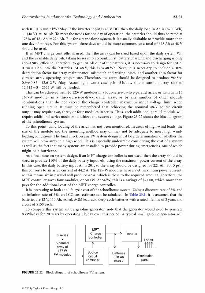
require additional series modules to achieve the system voltage. Figure 23.22 shows the block diagram
of the schoolhouse system.
To this point, wind loading of the array has not been mentioned. In areas of high-wind loads, the
size of the module and the mounting method may or may not be adequate to meet high wind-
loading conditions. The final check on any PV system design must be a determination of whether the
system will blow away in a high wind. This is especially undesirable considering the cost of a system
as well as the fact that many systems are installed to provide power during emergencies, one of which
might be a hurricane.
As a final note on system design, if an MPT charge controller is not used, then the array should be
sized to provide 110% of the daily battery input Ah, using the maximum power current of the array.
In this case, the daily battery input Ah is 201, so the array should be designed for 221 Ah. For 5 psh,
this converts to an array current of 44.2 A. The 125-W modules have a 7-A maximum power current,
so this means six in parallel will produce 42 A, which is close to the required amount. Therefore, the
MPT controller saves four modules, or 500 W. At $4/W, this is a savings of $2,000, which more than
pays for the additional cost of the MPT charge controller.
It is interesting to look at a life-cycle cost of the schoolhouse system. Using a discount rate of 5% and
an inflation rate of 3%, an LCC cost estimate can be tabulated. In Table 23.1, it is assumed that the
batteries are 12 V, 110 Ah, sealed, AGM lead-acid deep-cycle batteries with a rated lifetime of 8 years and
a cost of $150 each.
To compare this system with a gasoline generator, note that the generator would need to generate
8 kWh/day for 20 years by operating 8 h/day over this period. A typical small gasoline generator will
3 seriesx
5 parallelarray of167 W
PV modulesSourcecircuit
combiner
MPTCharge
controllerInverter
Batteries678 Ah@48 V
Distributionpanel
Loads
FIGURE 23.22 Block diagram of schoolhouse PV system.
q 2007 by Taylor & Francis Group, LLC

TABLE 23.1 Life-Cycle Costs of a Standalone Photovoltaic System for a Schoolhouse
Item Cost Present Worth % LCC
Capital Costs
Array $10,000 $10000 38.1
Batteries 3600 3600 13.7
Array mount 1250 1250 4.8
Controller 500 500 1.9
Inverter 500 500 1.9
BOS 1000 1000 3.8
Installation 2000 2000 7.6
Recurring Costs
Annual Inspection 50 839 3.2
Replacement Costs
Batteries K8 yr 3600 3087 11.8
Batteries K16 yr 3600 2646 10.1
Controller K10 yr 500 413 1.6
Inverter K10 yr 500 413 1.6
Totals $26,247 100
23-22 Handbook of Energy Efficiency and Renewable Energy
generate 4 kWh/gal (Messenger and Ventre 2004), so will require 2 gal of gasoline per day. The generator
will require an oil change every 25 h, a tune-up every 300 h and a rebuild every 3000 h. The LCC analysis
for the generator is shown in Table 23.2. Clearly, the PV system is the preferred choice. And this does not
account for the noise-free, pollution-free performance of the PV system.
23.1.8.3 A Straightforward Utility-Interactive PV System
Because utility-interactive PV systems are backed up by the utility, they do not need to be sized to meet
any particular load. Sometimes they are sized to meet emergency loads, but if the system does not have
emergency backup capabilities, then they may be sized to fit on a particular roof, to meet a particular
budget, or to incorporate a particular inverter. Suppose the sizing criteria is the inverter, which has the
following specifications:
TABLE 23.2 Life-C
Item
Capital Costs
Generator
Recurring Costs
Annual fuel
Annual oil changes
Annual tune-ups
Annual rebuilds
q 2007 by Taylor & Francis
DC Input
ycle Costs of a Gasoline Gen
C
$
1
Group, LLC
Input Voltage Range
erator for a Schoolhouse
ost Presen
750
825 30
235
345
146
$41
250–550 V
Maximum Input Current
11.2 AAC Output
Voltage 240 V 1fNominal Output Power
2200 WPeak Power
2500 WTotal Harmonic Distortion
! 4%Maximum Efficiency
94%Note that if the input voltage is 550 V and the input current is 11.2 A, the input power would be 6160 W.
Because the peak output power of this inverter is 2500 W, it would not make sense to use a 6160-W array
t Worth %LCC
$750 2
,593 73
3939 9
4107 10
2447 6
,836 100

Photovoltaics Fundamentals, Technology and Application 23-23
since most of the output would be wasted, and it might be easier to damage the inverter. Therefore, an
array size of about 2500 W would make better sense.
Because cloud focusing can increase the short circuit output current of a module by 25%, the array
rated short circuit current should be kept below 11.2O1.25Z8.96 A. The number of modules in series
will depend upon the maximum voltage of the array at low temperatures remaining less than 550 V and
the minimum array voltage at high array operating temperatures remaining greater than 250 V.
NEC Table 690.7 specifies multipliers for open-circuit voltages for different low-temperature ranges.
For design purposes, suppose the coldest array temperature will be K258C and the hottest array
temperature will be 608C. NEC Table 690.7 requires a multiplier of 1.25 for the array open-circuit voltage,
so the maximum rated array open circuit voltage must be less than 550O1.25Z440 V. If the open-circuit
voltage of a module decreases by 0.47%/8C, then it will decrease by 35!0.47Z16.45% when the module
is operated at 608C. Thus, the 258C-rated array open-circuit voltage needs to be greater than 250O
0.8355Z299 V.
The next step is to look at PV module specifications. One module has PmaxZ125 W, VOCZ21.0 V and
ISCZ7.2 A. Thus, the maximum number of these modules in series will be 440O21.0Z20.95, which
must be rounded down to 20. The minimum number in series will be 299O21.0Z14.24, which must be
rounded up to 15. Checking power ratings gives 2500 W for 20 modules and 1875 W for 15 modules.
Because 2500 W does not exceed the inverter rated maximum output power, and because the array will
normally operate below 2500 W, it makes sense to choose 20 modules, as long as the budget can afford it
and as long as there is room for 20 modules wherever they are to be mounted. Figure 23.15d shows the
block diagram for this system.
The life-cycle cost of this type of system is usually looked at somewhat differently than that of the
schoolhouse system. In this case, the cost of electricity generated is usually compared with the cost of
electricity from the utility, neglecting pollution and other externalities. In regions with an abundance of
trained installers, it is currently possible to complete a grid-connected installation for less than $7/W. The
installed cost of the 2500-W system would thus be approximately $17,500. It is reasonable to expect an
average daily output of 10 kWh for this system in an area with an average of 5 peak sun hours. The value
of the annual system output will thus be approximately $365 at $0.10/kWh. This amounts to a simple
payback period of 48 years—almost double the expected lifetime of the system.
Of course, what is not included in the analysis is the significant amount of CO2 production that is
avoided, as well as all the other pollutants associated with nonrenewable generation. Also not included
are the many subsidies granted to producers of nonrenewable energy that keep the price artificially low.
For that matter, it assumes that an abundance of fossil fuels will be available at low cost over the lifetime
of the PV system. Finally, it should be remembered that the energy produced by the PV system over the
lifetime of the system will be at least four times as much as the energy that went into the manufacture and
installation of the system.
If the cost of the system could be borrowed at 3% over a period of 25 years, the annual payments would
be $1005. Thus, if a grid-connected system is considered, unless there is a subsidy program, it could not
be justified with simple economics. It would be purchased simply because it is the right thing to do for
the environment. Of course, if the installation cost were less, the value of grid electricity were more and
the average sunlight were higher, then the numbers become more and more favorable. If the values of
externalities, such as pollution, are taken into account, then the PV system looks even better.
Because of the cost issue, as well as local PUC regulations or lack of them, ill-defined utility interface
requirements, etc., few grid-connected PV systems are installed in areas that do not provide some form
of incentive payments. In some cases, PV system owners are paid rebates based on dollars per watt.
The problem with this algorithm is that there is no guarantee that the system will operate properly. In
other cases, PV system owners are guaranteed a higher amount per kWh for a prescribed time, which
guarantees that the system must work to qualify for incentive payments. In fact, at present, more kW
of PV are installed annually in grid-connected systems than are installed in standalone systems
(Maycock, 2003).
q 2007 by Taylor & Francis Group, LLC

23-24 Handbook of Energy Efficiency and Renewable Energy
23.1.9 Latest Developments in PV
The PV field is developing rapidly. The latest developments of 2006 will be historic developments in 2008,
so it is almost presumptuous to claim what are the “latest” developments when it is likely that by the time
the reader sees this paragraph, the development will be history. Not only are significant developments
being made in PV cell technology, but significant developments in PV system component technology are
also being made. Several recent developments, however, are particularly notable, and other recent
developments may also become notable. Rather than attempt to identify all of the latest important
developments in PV, a few will be described here to foster sufficient curiosity in the reader to encourage
further reading of those publications, such as the Proceedings of the IEEE PV Specialists Conferences, in
which the latest developments are reported. Several additional publications that track new developments
in PV are listed in the reference section (Maycock; American Solar Energy Society; Renewable Energy
World; Goswami and Boer, International Solar Energy Society). Cost, efficiency, and reliability are the key
words that drive the PV system development process, whether applied to PV cells, modules, inverters,
array mounts, or other BOS components.
The current buzzword in crystalline silicon technology is “thin silicon.” The buried contact cell of the
University of New South Wales has been described earlier. Other processes that may show promise are
thin Si on ceramics (Green 2004), thin crystalline Si on glass (CSG) (Basore 2002a; Basore 2002b), and
epitaxially grown Si on existing crystalline Si with subsequent removal of the epitaxially grown cell from
the existing substrate (the PSI process) (Brendel et al. 2005). Combinations of crystalline and amorphous
Si are also showing very promising results. For example, the heterojunction with intrinsic thin-layer
(HIT) process has been used to fabricate a 21% efficient cell that has been incorporated into an 18.4%
module (Hamakawa 2005).
The interconnections of conventional Si cells add an additional processing step in module production.
Perhaps more importantly, these interconnects have led to cell failures due to interconnect failure.
Elimination of soldered interconnects through incorporating monolithic technology can lead to an
expedited production process, greater module reliability, and, perhaps more importantly, less sensitivity
of the module to shading because the cells extend the length of the module and have a relatively narrow
width. It is thus more difficult to entirely shade a single cell of a module.
Historically, inverters have been the weakest link of a PV system. Recently, the US Department of
Energy (2005) has sponsored the development of inverters designed to have at least a 10-year mean time
to failure. Thus, as the industry continues to mature, PV systems continue to come closer to simple
“plug-and-play” configurations that will be relatively simple to install and will require very little
maintenance over the projected 25-year lifetime of the system.
Recently, Green (2006) compiled a listing of the highest confirmed efficiencies for a range of
photovoltaic cell and module technologies. Table 23.3a was compiled from this reference and shows
the efficiency values of cells and the independent test centers where efficiencies were confirmed.
Table 23.3b shows similar information for modules. As expected, the module efficiencies are less than
the cell efficiencies.
23.1.10 Future Challenges for PV Systems
The PV industry is currently engaged in an effort to ensure quality control at all levels of system
deployment, including manufacturing, distribution, design, installation, inspection and maintenance. At
this point in time (2005), most of the technical challenges for PV system components have been
overcome. PV modules are very reliable, and most are warranted for 25 years. Reliability of other system
components continues to improve and, at this point, PV system power conditioning equipment has
proven to operate very reliably. Therefore, once installed properly, modern PV systems require very little
maintenance. In fact, systems without batteries require almost no maintenance.
To meet the design challenge, many manufacturers and distributors are offering “kits” with
standardized components and installation instructions. Although these systems meet many needs,
q 2007 by Taylor & Francis Group, LLC

TABLE 23.3a Confirmed Terrestrial Cell and Submodule Efficiencies Measured Under the Global AM1.5 Spectrum (1,000 WmK2)
Classificationa Effic. Description (%)b Area (cm2)c Voc (V) Jsc (mA/cm2) FF (%)d Test Center (and Date)e
Silicon
Si (crystalline) 24.7G0.5 4.00 (da) 0.706 42.2 82.8 Sandia (3/99)
UNSW PERL
Si (multicrystalline) 20.3G0.5 1.002 (ap) 0.664 37.7 80.9 NREL (5/04)
FhG-ISE
Si (thin-film transfer) 16.6G0.4 4.017 (ap) 0.645 32.8 78.2 FhG-ISE (7/01)
U. Stuttgart (45 mm
thick)
Si (amorphous)f 9.5G0.3 1.070(ap) 0.859 17.5 63.0 NREL (4/03)
U. Neuchatel
Si (nanocrystalline) 10.1G0.2 1.199(ap) 0.539 24.4 76.6 JQA (12/97)
Kaneka (2 mm on glass)
III–V Cells
GaAs (crystalline) 25.1G0.8 3.91(t) 1.022 28.2 87.1 NREL (3/90)
Kopin, AlGaAs window
GaAs (thin-film) 24.5G0.5 1.002(t) 1.029 28.8 82.5 FhG-ISE (5/05)
Radboud U., NL
GaAs (multicrystalline) 18.2G0.5 4.011(t) 0.994 23.0 79.7 NREL (11/95)
RTI, Ge substrate
InP (crystalline) 21.9G0.7 4.02(t) 0.878 29.3 85.4 NREL (4/90)
Spire, epitaxial
Thin-film chalcogenide
CIGS (cell) 18.4G0.5g 1.04(ap) 0.669 35.7 77.0 NREL (2/01)
NREL, CIGS on glass
CIGS (submodule) 16.6G0.4 16.0(ap) 2.643 8.35 75.1 FhG-ISE (3/00)
U. Uppsala, 4 serial cells
CdTe (cell) 16.5G0.5g 1.032(ap) 0.845 25.9 75.5 NREL (9/01)
NREL, mesa on glass
Photochemical
Nanocrystalline dye 10.4G0.3 1.004 (ap) 0.729 21.8 65.2 AIST(8/05)
Sharp
Nanocrystalline dye 4.7G0.2 141.4 (ap) 0.795 11.3 59.2 FhG-ISE (2/98)
INAP
(submodule)
(continued)
Ph
oto
volta
ics
Fu
nd
am
en
tals,
Tech
nolo
gy
an
dA
pplic
atio
n2
3-2
5
q 2007 by Taylor & Francis Group, LLC

TABLE 23.3a (Continued)
Classificationa Effic. Description (%)b Area (cm2)c Voc (V) Jsc (mA/cm2) FF (%)d Test Center (and Date)e
Multijunction devices
GaInP/GaAs/Ge 32.0G1.5 3.989(t) 2.622 14.37 85.0 NREL (1/03)
Spectrolab (monolithic)
GaInP/GaAs 30.3 4.0(t) 2.488 14.22 85.6 JQA (4/96)
Japan Energy
(monolithic)
GaAs/CIS (thin-film) 25.8G1.3 4.00(t) – – – NREL (11/89)
Kopin/Boeing (4
terminal)
a-Si/CIGS (thin-film)h 14.6G0.7 2.40(ap) – – – NREL (6/88)
ARCO (4 terminal)
a-Si/mc-Si (thin
submodule)i11.7G0.4 14.23(ap) 5.462 2.99 71.3 AIST (9/04)
a CIGSZCuInGaSe2; a-SiZamorphous silicon/hydrogen alloy.b Effic.Zefficiency.c (ap)Zaperture area; (t)Ztotal area; (da)Zdesignated illumination area.d FFZfill factor.e FhG-ISEZFraunhofer-Insitut fur Solare Energiesysteme; JQAZJapan Quality Assurance; AISTZJapanese National Institute of Advanced Industrial Science and Technology.f Stabilized by 800 h, 1 sun AM1.5 illumination at a cell temperature of 508C.g Not measured at an external laboratory.h Unstabilized results.i Stabilized by 174 h, 1-sun illumination after 20 h, 5-sun illumination at a sample temperature of 508C.
Source: From Deng, X. and Schiff, E. A., Amorphous silicon-based solar cells, In Handbook of Phtovoltaic Science and Engineering, Luque, A. and Hegedus, S., eds., Wiley, New York, 2003.
23
-26
Han
db
ook
of
En
erg
yE
fficie
ncy
an
dR
en
ew
ab
leE
nerg
y
q 2007 by Taylor & Francis Group, LLC

TABLE 23.3b Confirmed Terrestrial Module Efficiencies Measured Under the Global AM1.5 Spectrum (1,000 W/m2) and at 258C
Classificationa Effic. Description (%)b Area (cm 2)c Voc (V) I sc (A) FF (%)d Test Center (and Date)
Si (crystalline) 22.7G0.6 778 (da) 5.60 3.93 80.3 Sandia (9/96)
UNSW/Gochermann
Si (multicrystalline) 15.3G0.4e 1017 (ap) 14.6 1.36 78.6 Sandia (10/94)
Sandia/HEM
Si (thin-film
polycrystalline)
8.2G0.2 661 (ap) 25.0 0.318 68.0 Sandia (7/02)
Pacific Solar (1–2 mm on
glass)
CIGSS 13.4G0.7 3459(ap) 31.2 2.16 68.9 NREL (8/02)
Showa Shell (Cd free)
CdTe 10.7G0.5 4874(ap) 26.21 3.205 62.3 NREL (4/00)
BP Solarex
a-Si/a-SiGe/a-SiGe
(tandem)f10.4G0.5 905(ap) 4.353 3.285 66.0 NREL (10/98)
USSC (a-Si/a-Si/a-
Si:Ge)
a CIGSSZCuInGaSSe; a-SiZamorphous silicon/hydrogen alloy; a-SiGeZamorphous silicon/germanium/hydrogen alloy.b Effic.Zefficiency.c (ap)Zaperture area; (da) Zdesignated illumination area.d FFZfill factor.e Not measured at an external laboratory.f Light soaked at NREL for 1000 h at 508C, nominally 1-sun illumination.
Ph
oto
volta
ics
Fu
nd
am
en
tals,
Tech
nolo
gy
an
dA
pplic
atio
n2
3-2
7
q 2007 by Taylor & Francis Group, LLC

23-28 Handbook of Energy Efficiency and Renewable Energy
there are still needs for custom systems, and design professionals are still generally unfamiliar with PV
system design. In some areas where PV systems have been encouraged, there are properly trained
installers and maintenance personnel. But in most areas, it is difficult to find a contractor who is familiar
with PV systems. It is not unusual for a general contractor to oppose the installation of a PV system out
of fear that it may compromise structural integrity. Furthermore, once a system is installed, it is usually
difficult to find someone who understands PV systems well enough to be able to inspect a system for code
compliance. It is also difficult to find someone who can troubleshoot a nonfunctional system, or, for that
matter, to determine that a system is not working up to specifications. Therefore, in the case of design,
installation, inspection and maintenance, there is a lot of education and training to accomplish.
There are also some nontechnical challenges. One is cost. The installed cost of a PV system is still three
to six times as high as the installed cost of conventional nonrenewable generation. As fuel costs rise and as
PV installed costs decrease, it is likely that within a decade, the two costs may become equal, especially if
fuel and environmental costs are taken into account. If the cost of a PV system were to be measured in
Btus, then perhaps the importance of PV systems would become more obvious. By the early 1980s,
Odum and Odum (1981); Henderson (1981) had proposed using the Btu as the international monetary
standard. Recently, Messenger and Ventre (2004) report a conservative factor of 4:1 return on the Btus
expended in the deployment of a PV system, and Battisti and Corrado (2005) report energy payback
times (EPBT) of approximately three years and CO2eq payback times of about four years for PV systems.
Because the life expectancy of a PV system exceeds 20 years, this equates to about a 7:1 return on the Btu’s
invested and a 5:1 return on avoidance of CO2 and equivalent greenhouse gases released during the
production and installation phase of a PV system. These positive return on investment figures make PV a
very attractive energy source and suggest that the dollar cost of a PV system does not adequately portray
the true environmental value of a PV system.
In a recent review paper, Hamakawa (2005) reported that in 2000, commercial silicon PV module
efficiency was 13%–14% and the cost about 300 Yen/W (approximately $3–$4/W). He predicted that by
2010 the module efficiency would go up to 17% and the cost would come down to 100 Yen/W
(approximately $1/W) and by 2015–2020 the module efficiency will increase to 20% with the costs down
to 75 Yen/W (approximately 75 cents/W). Based on the progress in research as reported by Green (2004),
where thin-film cell efficiencies of 24.7% were achieved in 2003, it is not too difficult to imagine that
Hamakawa’s predictions about module efficiencies may be on target. Only the future will tell whether the
cost predictions will be realized or not; however, it is clear that the costs are moving in the right direction.
23.2 Thin-Film PV Technology
Hari M. Upadhyaya, Takhir M. Razykov, and Ayodhya N. Tiwari
23.2.1 Introduction
23.2.1.1 Historical and Current Developments
Crystalline silicon (c-Si) technology has a lion’s share in the present photovoltaic (PV) industry,
contributing more than 95% through the cells and modules based on mono- and multicrystalline wafer
technology. The recent growth rate of the photovoltaic industry and market is phenomenal, with a
substantial surge of over 30%–40% recorded globally during last few years. During the early
developmental phase of c-Si PV technology, the continuous feedstock support offered by the Si-based
electronics industry played a key role in its growth. The high-purity and even second-grade wafer
materials obtained at a relatively cheaper price proved favorable for the PV industry, as they led to a
reasonable efficiency (average hO15%) and extremely good performance stability (more than 25 years)
that are two essential requirements for any technology to successfully demonstrate its potential (Chopra
et al. 2004; Jager-Waldau 2004). However, continuously increasing demand for PV modules and the need
for low-cost PV options have stretched these advantages to the limit and have exposed some inherent
q 2007 by Taylor & Francis Group, LLC

Photovoltaics Fundamentals, Technology and Application 23-29
disadvantages of c-Si technology, such as the scarcity of feedstock material and costly processing of
materials and device fabrication steps, as well as the inability for monolithic interconnections. These, in
turn, restrict the potential of Si wafer technology and make it difficult to achieve PV module production
cost below V 1/W (1V is about US$1.20), which is considered essential for cost-competitive generation
of solar electricity (Hegedus and Luque 2003; von Roedern et al. 2005; Zweibel 2000). The PV module
cost depends on the total manufacturing cost of the module per square area, conversion efficiency, and
long-term performance stability. Figure 23.23 gives an estimate of achievable cost with c-Si technology
and a comparison with projected achievable costs with other PV technologies. It is generally agreed that
c-Si wafer technology would be unable to meet the low cost targets, whereas thin-film technologies have
the potential to provide a viable alternative in the near future.
In addition, Si wafers are fragile, solar cell area is limited by the wafer size, and the modules are bulky,
heavy, and nonflexible. To overcome some of the problems of c-Si wafer technology, efforts are being
made to develop monocrystalline and polycrystalline thin-film silicon solar cells, as reviewed by
Bergmann (1999).
It has been realized that application of thin-film technologies to grow solar cells and modules based on
other materials can solve some of the problems of the silicon-wafer technologies. Thin-film deposition of
materials of required quality and suitable properties depends on the processes used and the control of
several parameters. However, once optimized, these methods provide over an order of magnitude
cheaper processing cost and low-energy payback time, which is certainly a big advantage.
Research on alternatives to c-Si started about four decades back. It has a low-absorption coefficient
(w103 cmK1) and its bandgap (Eg w1.1 eV) is far below than the optimum Eg w1.5 eV required for
high solar-electric conversion using a single-junction solar cell. Some of the most interesting
semiconducting materials that have received considerable attention are: cadmium telluride (CdTe),
gallium arsenide (GaAs), indium phosphide (InP), zinc phosphide (Zn3P2), copper sulfide (Cu2S),
copper indium diselenide (CIS), and copper–indium gallium diselenide (CIGS). These all have the
electronic and optical properties suitable for the efficient utilization of the sun’s spectrum
(see Table 23.4 for bandgaps). Multijunction solar cells based on III–V materials (GaAs, InP, GaSb,
GaInAs, GaInP, etc.) show high efficiency, exceeding 35%, but due to the high production costs and low
availability of their constituents, these solar cells are not considered suitable for cost-effective terrestrial
applications, although they are still very important for space PV applications.
Thin-film technology has answers and potential to eliminate many existing bottlenecks of c-Si PV
programs, which are experienced at different levels from module production to its application. Thin-film
100
90
80
70
60
50
40
30
20
10
0Glass
Cost, /m2
1.00 / Wp
0.50 / WpThermodynamic
limit
0.20 / Wp 0.10 / Wp
Effi
cien
cy, %
3.50 / Wp
100 200 300 400 500
0
1: Crystalline silicon2: Thin-films3: Beyond horizon
12
3
FIGURE 23.23 Comparison of estimated costs achievable with different PV technologies as a function of
manufacturing cost (V/m2) and conversion efficiency. (Courtesy M. Green, UNSW.)
q 2007 by Taylor & Francis Group, LLC

TABLE 23.4 Bandgaps of Different Semiconductor Materials Suitable as Light Absorber in Solar Cells
Compound/Alloys Bandgap (eV) Compound/Alloys Bandgap (eV)
c-Si 1.12 Zn3P2 1.50
a-Si 1.70 CuInSe2 1.04
GaAs 1.43 CuGaSe2 1.68
InP 1.34 Cu(In,Ga)Se2 1.20
Cu2S 1.20 CuInS2 1.57
CdTe 1.45 Cu(In,Ga)(S,Se)2 1.36
23-30 Handbook of Energy Efficiency and Renewable Energy
PV modules are manufactured on either rigid glass substrates or flexible substrates (thin metallic or plastic
foils). Some of the advantages of the thin-film technologies are:
† The high-absorption coefficient (w105 cmK1) of the absorber materials is about 100 times higher
than c-Si (Figure 23.24); thus about 1–2 mm of material thickness is sufficient to harness more than
90% of the incident solar light. This helps in reducing the material mass significantly to make
modules cost-effective. The estimated energy payback time of the thin-film PV is 3–5 times lower
than that of c-Si PV.
† The formation of heterojunction and better device engineering for reduction of photon
absorption losses and enhanced collection of photogenerated carriers are possible.
† Large-area deposition (on the order of m2), along with the monolithic integration (inter-
connection of cells during processing of rigid and flexible devices) is possible which minimizes
area losses, handling, and packaging efforts.
† Roll-to-roll manufacturing of flexible solar modules is possible. This gives high throughput and
thus can reduce the energy payback time significantly.
† Tandem/multijunction devices could be realized to utilize the full solar spectrum to achieve
higher-efficiency (greater than 50%) devices.
† Flexible and lightweight PV facilitates several attractive applications.
0.5
107
106
105
104
103
102
101
100
10−1
1 1.5Photon energy [eV]
α [c
m−1
]
2 2.5
a-Si:Hµc-Si:Hc-SiCu(In,Ga)Se2CuInSe2
CdTe
3 3.5
FIGURE 23.24 The optical absorption (a) versus bandgap (Eg) spectra of the c-Si and other prominent light-
absorbing materials that are used in thin-film solar cells.
q 2007 by Taylor & Francis Group, LLC

a-Si/μ-Si,8%
CIGS, 7%
CdTe indoor, 4%
CdTe outdoor, 7%
a-Si indoor, 18%
a-Si outdoor
FIGURE 23.25 Worldwide sales of thin-film solar cells in 2002 were 43.8 MW. (From Maycock, P. D. Renewable
Energy World, 6, 84–101, 2003.)
Photovoltaics Fundamentals, Technology and Application 23-31
Historically, cadmium sulfide and copper sulfide (CdS/Cu2S) heterojunctions were one of the early
technologies, almost contemporary to c-Si, but could not survive due to the astounding success of c-Si
technology that was efficient, stable, backed by electronic industries, and widely supported by space
programs. Despite CuxS having stability problems, the technology went to pilot production in the late
1970s or early 1980s, but with the advent of a-Si and CdTe thin-film solar cells, it was abandoned before
the mid 1980s.
Currently, a-Si, CdTe, and CIGS are considered the mainstream thin-film technologies. Out of these, a-
Si currently has the highest market share (Figure 23.25), as with the involvement of several industries
worldwide during the last two decades, this technology has attained a significant level of maturity for
large volume production. In addition, CdTe and CIGS have proven their potential to become leading
technologies but they lacked adequate R&D and industrial and investors’ support to make a mark.
However, recently several companies have started production-related activities and production volume is
expected to increase during the next few years. Recent developments on a new technology for organic and
dye-sensitized solar cells appear to be quite interesting with their low-temperature and cheaper
processing cost on flexible substrates (Gratzel 2000; Durr et al. 2005). However, there are potential
issues of instability and degradation. They are in the infancy of their development at the moment and
would require considerable efforts and time to see them become a commercially viable option.
Figure 23.26 (von Roedern et al. 2005) summarizes the best laboratory-scale (cell area less than 1 cm2)
efficiencies of some prominent thin-film technologies. Out of these, an efficiency of 19.5% achieved at
NREL, USA with CIGS makes it the most efficient thin-film PV device, which has narrowed the gap
further between existing c-Si and thin-film technologies. Table 23.5 summarizes the current status of
thin-film solar cell and module development at laboratory and industrial levels on rigid substrates (with
one exception). These contain some of the latest developments and global efforts to make thin-film PV
technology a viable option for cost-effective and competitive electrical energy production.
23.2.1.2 Cost Potentials and Material Availability Issues
Estimates suggest that solar cell production costs below 1 V/W to up to 0.30 V/W are possible depending
on the volume of production (Bruton et al. 1997; Keshner and Arya 2004; Woodcock et al. 1997). At
present, there is a significantly large gap between the efficiencies of the solar cells at the R&D level, and
those at the industrial modules level, because of the process-scalability-related problems during the early
phase of industrial development. The current production cost of the thin-film PV modules is rather high
because of low volume of production through pilot-production lines or small-capacity (less than
30 MW) plants. However, with larger production volumes and higher module efficiencies, the cost is
q 2007 by Taylor & Francis Group, LLC
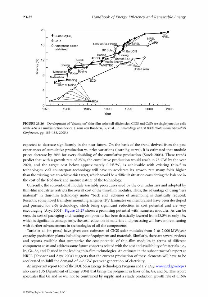
Cu(In,Ga)Se2
CdTe
Amorphous silicon(stabilized)
Univ. of Maine
Boeing
Boeing
Boeing
BoeingARCO
AMETEK
NREL
BoeingEuroCIS
Univ. of So. Florida
Univ.of So.FL
BP Solar
Kodak
Kodak
Year
Monosolar
Effi
cien
cy (
%)
Matsushita
12
8
4
0200019951990198519801975
United solar
16
20
NREL
2005
RCA
ECD
NREL
Photon Energy
FIGURE 23.26 Development of “champion” thin-film solar cell efficiencies. CIGS and CdTe are single junction cells
while a-Si is a multijunction device. (From von Roedern, B., et al., In Proceedings of 31st IEEE Photovoltaic Specialists
Conference, pp. 183–188, 2005.)
23-32 Handbook of Energy Efficiency and Renewable Energy
expected to decrease significantly in the near future. On the basis of the trend derived from the past
experiences of cumulative production vs. price variations (learning curve), it is estimated that module
prices decrease by 20% for every doubling of the cumulative production (Surek 2003). These trends
predict that with a growth rate of 25%, the cumulative production would reach w75 GW by the year
2020, and the target cost below approximately 0.2V/Wp is achievable with existing thin-film
technologies. c-Si counterpart technology will have to accelerate its growth rate many folds higher
than the existing rate to achieve this target, which would be a difficult situation considering the balance in
the cost of the feedstock and mature nature of the technology.
Currently, the conventional module assembly procedures used by the c-Si industries and adopted by
thin-film industries restricts the overall cost of the thin-film modules. Thus, the advantage of using “less
material” in thin-film technology under “back end” schemes of assembling is drastically reduced.
Recently, some novel frameless mounting schemes (PV laminates on membranes) have been developed
and pursued for a-Si technology, which bring significant reduction in cost potential and are very
encouraging (Arya 2004). Figure 23.27 shows a promising potential with frameless modules. As can be
seen, the cost of packaging and framing components has been drastically lowered from 25.5% to only 4%,
which is significant; consequently, the cost reduction in materials and processing will have more meaning
with further advancements in technologies of all the components.
Tuttle et al. (in press) have given cost estimates of CIGS solar modules from 2 to 2,000 MW/year
capacity production plants including cost of equipment and materials. Similarly, there are several reviews
and reports available that summarize the cost potential of thin-film modules in terms of different
component costs and address some future concerns related with the cost and availability of materials, i.e.,
In, Ga, Se, and Te used in the leading thin-film technologies. An estimate in the subcontractor’s report at
NREL (Keshner and Arya 2004) suggests that the current production of these elements will have to be
accelerated to fulfil the demand of 2–3 GW per year generation of electricity.
An important report (out of the DOE Solar Energy Technologies Program and PV FAQ, www.nrel.gov/ncpv)
also exists (US Department of Energy 2004) that brings the judgment in favor of In, Ga, and Se. This report
speculates that Ga and Se will not be constrained by supply, and a steady production growth rate of 0.16%
q 2007 by Taylor & Francis Group, LLC

TABLE 23.5 Efficiencies of Solar Cells and Modules Based on Rigid Substrates (With the Exception of USSC Cells on Steel) with Their Configuration for Various Technologies
Material/Cell
configuration
Companies
Institutions/
Laboratory
Cell/Modules
Area (cm2) Power (Watts) Test Center/Date Remarks/References
Efficiency (%)
a-Si/a-SiGe/nc-SiGe USSC 13.0(14.6)a 0.25 03/05 (Stainless steel substrate)
a-Si/a-SiGe USSC 12.4 0.25 10/04 (Stainless steel substrate)
a-Si Uni. Neuchatel 9.5 1.07 NREL (1/03) Stabilized at 800 h
a-Si/m-Si (submodule) IPV Juelich 10.1(10.7)a 100 06/04 Stabilized at 1000 h
a-Si/a-SiGe/a-SiGe/SS United Solar 7.6 9276 70.8 NREL (9/97)
a-Si/a-SiGe/a-SiGe BP Solarex 10.4 905 NREL(10/98)
a-Si Mitsubishi Heavy 6.4 15625 100 (7/ 05)
a-Si Kaneka 6.3 8100 51 NREL (7/04)
a-Si/a-Si EPV 5.7 7432 42.3 NREL (10/02)
a-Si/ nano-Si Sharp 11 4770 52.5 (7/05)
a-Si/m-Si (submodule) Kaneka 11.7 14.23 AIST(9/04)
mc Si (polycrystalline) Pacific Solar 8.2 661 Sandia (7/02)
CdS/CdTe NREL 16.5 1.032 NREL (9/01)
CdS/CdTe BP Solarex 10.7 4874 NREL (4/00)
CdS/CdTe First Solar 10.2 6624 67.4 (2/04)
CdS/CdTe Antec Solar 7.3 6633 52.3 (6/04)
CdS/CdTe BP Solar 11.0 8390 92.5 NREL (9/01)
CdS/CdTe Matsushita 11.0 5413 59 NREL (6/00)
CdS/CIGS NREL 19.5 0.41 FhG-ISE (9/04)
CdS/CIGS
(submodule)
Univ. of Uppsala 16.6 16.0 FhG-ISE (3/00)
CIGSS Showa Shell 13.4 3459 NREL (8/02) (Cd free)
CdS/ CIGS/SS Global Solar 10.2 8709 88.9 NREL (5/05)
CdS/CIGS/Glass Wurth Solar 13.0 6500 84.6 NREL (6/04)
CdS/ CIS-alloy/Glass Shell Solar GmbH 13.1 4938 64.8 NREL (6/04)
CdS/ CIS-alloy/Glass Shell Solar Ind. 12.8 3626 46.5 NREL (3/03)
ZnS(O.OH)CIGS/Glass
Showa shell 13.4 3459 46.45 NREL (8/02)
DSSC EPFL, Lausanne 11.0 0.25 FhG-ISE (9/04) Nanocrystalline TiO2 (Gratzel, 2000)
DSSC ECN 8.2 2.36 FhG-ISE (7/01)
DSSC(submodule) INAP 4.7 141.4 FhG-ISE (2/98)
a Measured efficiency before light-induced degradation.
Ph
oto
volta
ics
Fu
nd
am
en
tals,
Tech
nolo
gy
an
dA
pplic
atio
n2
3-3
3
q 2007 by Taylor & Francis Group, LLC

(a)
Packaging
4.0% Substrate
26.9%
Thin-films27.7%
Lamination20.8%
Connectors& wiring
20.6%
21.5%
Frames and packaging
25.5%
Substrate20.9%
Thin-films
Lamination16.1%
Connectors& wiring
16.0%
(b)
FIGURE 23.27 Distribution and break-up of the materials cost in (a) framed and (b) unframed a- Si based
modules.
23-34 Handbook of Energy Efficiency and Renewable Energy
per year for Se would be sufficient to meet the demand of annual PV production of 20 GW/year by 2050.
Furthermore, it is also estimated that there will be a steady supply of In as it is a by-product of Zn, which
is relatively higher in abundance and more in demand in various industries. There could be some
concerns about the availability of Te for multi-GW plants, but with the advancement in thin-film
technology, the thickness of the material may be reduced by implementation of light trapping schemes,
thus relieving the burden on production of materials.
In the following sections, the front-line thin-film technologies such as a-Si, CdTe, and CIGS are
discussed in detail relating to their material and device aspects, current status, and issues related to
environmental concerns.
23.2.2 Thin-Film Silicon
23.2.2.1 Material and Properties
The oil crisis of the early 1970s gave an impetus to the PV R&D activities and several concepts for thin-
film PV started emerging. The first report on thin-film a-Si-based solar cells appeared in 1976 (Carlson
and Wronski 1976). It took only five years to see the indoor consumer products appearing in the market
with this technology in the 1980s, although it took a significant amount of time to understand the basics
of the material and device properties and their inherent bottlenecks. Amorphous-Si is now the most
studied and applied material for thin-film solar cells as compared to its counterparts. Silicon has the
advantage of the material being in abundance in the earth’s crust; therefore, following the trends of c-Si
technology, a-Si has developed over the years into an industrially mature technology (Rech and Wagner
1999). In addition, a-Si has several other non-PV applications that provide it an additional standing.
Crystalline-Si has long-range atomic ordering extending up to a few cm in single crystals, whereas a-Si
exhibits short-range atomic ordering of less than 1 nm, and thus the material is not a crystal. Amorphous
silicon has a disordered lattice showing localized tetrahedral bonding schemes but with broken Si-Si bonds
of random orientation, as shown in Figure 23.28. These broken (or unsaturated) bonds are called “dangling
bonds” and contribute to the defect density in the material. Because of disorder, the momentum
conservation rules are relaxed and a higher absorption coefficient (a) is observed in a-Si materials. The
absorption coefficient of a-Si is about two orders of magnitude higher than c-Si, thus it only requires a
couple of microns of thickness for effective absorption and utilization of the solar spectrum. However, due
to its predominant disordered structure, a high density (w 1019 cmK3) of localized defect states are created
within the energy gap that causes the Fermi-level pinning. Hence, the material cannot be doped because the
defects states act as a trap for all free carriers generated in the material.
One effective way to overcome this problem is to passivate the unsaturated bonds of a-Si with the help
of small atoms that could get into the crystal and attach themselves with the available bonds. This is
precisely done by adding 5%–10% atomic hydrogen into a-Si, which attaches itself to the uncoordinated
bonds due to its high activity; this reduces the dangling bonds density from w1019 to w1015 cmK3.
q 2007 by Taylor & Francis Group, LLC
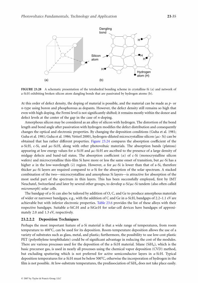
Hydrogenatom (H)
Danglingbond
H
H
HHSilicon
atom
(b)(a)
FIGURE 23.28 A schematic presentation of the tetrahedral bonding scheme in crystalline-Si (a) and network of
a-Si:H exhibiting broken silicon atom dangling bonds that are passivated by hydrogen atoms (b).
Photovoltaics Fundamentals, Technology and Application 23-35
At this order of defect density, the doping of material is possible, and the material can be made as p- or
n-type using boron and phosphorous as dopants. However, the defect density still remains so high that
even with high doping, the Fermi level is not significantly shifted; it remains mostly within the donor and
defect levels at the center of the gap in the case of n-doping.
Amorphous silicon may be considered as an alloy of silicon with hydrogen. The distortion of the bond
length and bond angle after passivation with hydrogen modifies the defect distribution and consequently
changes the optical and electronic properties. By changing the deposition conditions (Guha et al. 1981;
Guha et al. 1981; Guha et al. 1986; Vetterl 2000), hydrogen-diluted microcrystalline silicon (mc- Si) can be
obtained that has rather different properties. Figure 23.24 compares the absorption coefficient of the
a-Si:H, c-Si, and mc-Si:H, along with other photovoltaic materials. The absorption bands (plateau)
appearing at low energy values for a-Si:H and mc-Si:H are ascribed to the presence of a large density of
midgap defects and band-tail states. The absorption coefficient (a) of c-Si (monocrystalline silicon
wafers) and microcrystalline thin-film Si have more or less the same onset of transition, but mc-Si has a
higher a in the low-wavelength (l) region. However, a for mc-Si is lower than that of a-Si, therefore
thicker mc-Si layers are required compared to a-Si for the absorption of the solar spectrum. A stacked
combination of the two—microcrystalline and amorphous Si layers—is attractive for absorption of the
most useful part of the spectrum in thin layers. This has been successfully employed, first by IMT
Neuchatel, Switzerland and later by several other groups, to develop a-Si/mc-Si tandem (also often called
micromorph) solar cells.
The bandgap of a-Si can also be tailored by addition of O, C, and Ge to produce amorphous materials
of wider or narrower bandgaps, e.g., with the addition of C and Ge in a-Si:H, bandgaps of 2.2–1.1 eV are
achievable but with inferior electronic properties. Table 23.6 provides the list of these alloys with their
respective bandgaps. Suitable a-SiC:H and a-SiGe:H for solar-cell devices have bandgaps of approxi-
mately 2.0 and 1.3 eV, respectively.
23.2.2.2 Deposition Techniques
Perhaps the most important feature of a-Si material is that a wide range of temperatures, from room
temperature to 4008C, can be used for its deposition. Room-temperature deposition allows the use of a
variety of substrates such as glass, metal, and plastic; furthermore, the possibility to use low-cost plastic
PET (polyethylene terephthalate) could be of significant advantage in reducing the cost of the modules.
There are various processes used for the deposition of the a-Si:H material. Silane (SiH4), which is the
basic precursor gas, is used in nearly all processes using the chemical vapor deposition (CVD) method,
but excluding sputtering which is not preferred for active semiconductor layers in a-Si:H. Typical
deposition temperatures for a-Si:H must be below 5008C, otherwise the incorporation of hydrogen in the
film is not possible. At low-substrate temperatures, the predissociation of SiH4 does not take place easily.
q 2007 by Taylor & Francis Group, LLC

TABLE 23.6 Energy Bandgaps (Eg) of Certain Alloys of a-Si:H with Germanium and
Carbon Used in Multiple Junction Solar Cell Structures
Material (Semiconductor/Alloy) Eg min (eV) Eg max (eV)
c-Si 1.1 1.1
mc-Si:H 1.0 1.2
a-Si:H 1.7 1.8
a-SiC:H 2.0 (in 20% C) 2.2
a-SiGe:H 1.3 (in 60% Ge) 1.7
a-Ge:H 1.1
23-36 Handbook of Energy Efficiency and Renewable Energy
Hence, room-temperature-deposited layers give rise to inferior quality and efficiency. Therefore, plasma
is used for dissociation of silane gas. Two of the most commonly used methods are plasma-enhanced
chemical vapor deposition (PECVD) and glow-discharge CVD. Typically, 13.56-MHz plasma excitation
frequencies with optimal plasma excitation power at 0.1–1 mbar pressure are used. SiH4 diluted with
hydrogen (w10%) is used in the deposition of a-Si:H, whereas increasing hydrogen dilution results in
mc-Si:H layers, but with lower growth rates. The typical deposition rates for a-Si cells (in R&D) is w1 A/s
and results in fairly long deposition times (50 min for 0.3-mm-thick a-Si:H cell, and 5 h for a 1.8-mm-
thick mc-Si:H cell), while 3 A/s or higher deposition rates are generally preferred in production plants.
For high deposition rates, the deposition technologies based on very-high-frequency (VHF), microwave,
and high-pressure plasma are currently being pursued at the R&D level. Rates as high as 10 A/s have been
achieved at laboratory scale.
Alternative deposition methods using the hot-wire CVD (HWCVD) technique, electron cyclotron
resonance reactor (ECR), and the combination of HWCVD and PECVD are also being carried out to
increase the deposition rate. A detailed account of some of these techniques can be found in the following
references: Carabe and Gandia (2004); Deng and Schiff (2003); Klein et al. (2004); Lechner and Schade
(2002); Shah et al. (2004), and Sopori (2003).
23.2.2.3 Amorphous-Silicon Solar Cells and Configurations
The conventional p–n junction configuration for a-Si:H-based solar cells suffers from inherent limitations
due to the presence of a large number of defect states even after H-passivation. The doping of a-Si:H further
increases this concentration, which reduces the average lifetime of the free carriers as a result of very high
recombination probabilities and low-diffusion lengths (w0.1 micron). Thus solar cells in the p–n
configuration do not work and are not considered suitable. The basic structure of a-Si solar cell
configuration is a p–i–n junction shown in Figure 23.29a, which illustrates qualitatively the thickness of
different layers grown in the device in the “superstrate” configuration, along with applied texturing
(roughness) of the transparent conducting electrodes for enhanced light trapping in the a-Si layer, as will be
described later.
The p–i–n type configuration for an a-Si solar cell was introduced by Carlson et al. at RCA
Laboratories, U.S.A. (Carlson and Wronski 1976), where an intrinsic (i) layer of a-Si:H is sandwiched
between the n- and p-type doped layers of a-Si:H or its alloys. Because of the very short lifetime (or high
recombination) of the carriers, the doped layers do not contribute to the photocurrent generation; i.e.,
the photons absorbed in these layers contribute to optical losses, but these p- and n-layers build up the
electrical field across the i-layers. This electrical field drives the electrons and holes in the opposite
direction. They are then photogenerated in the i-layer, which essentially acts as the absorber layer in a-
Si:H solar cells. The electrical field depends on the doping concentration of the p- and n-layers, as well as
the thickness, of the i-layer. Because the p- and n-doped layers do not contribute to the photocurrents
and can cause further recombination of the generated carriers before sweeping across the layer, it is
essential to minimize their thickness which is typically 10–30 nm. There is an upper limit to the thickness
of the i-layer (w0.5 micron), because charge defects reduce the effective field; thus, if the width of the
q 2007 by Taylor & Francis Group, LLC

(a) (b)
EVA
Glass
Incident light
i-Si
Metal back reflector
TCO
p-Si
n-Si
TCO
Conductionbandminimum
Valencebandmaximum
Fermi level
Ene
rgy
p-type intrinsic (i) n-type
FIGURE 23.29 The schematic representation of single junction a-Si solar cell in superstrate configuration (a) and
the energy band diagram of the p–i–n solar cell structure (b). EVA (Vinyl Acetate) is the polymer coating used for
encapsulation of the solar cell.
Photovoltaics Fundamentals, Technology and Application 23-37
i-layer exceeds the space charge width, then the extra width would act as a “dead” layer without actually
contributing to the photocurrent.
Stability and Recombination Issues in a-Si Solar Cells. The initial results of a-Si cells in the 1970s
indicated very promising potential for attaining efficiencies well above 10%. However, it was soon
observed and realized that a-Si solar cells suffer from an inherent problem of light-induced degradation
on their performance under continuous light exposure, later attributed to the Staebler-Wronsky effect
(SWE) (Staebler and Wronski 1977). It was observed that in a time scale of a few months, the
performance of the cells dropped about 30%–40% then stabilized at an efficiency lower than the
initial values. This initial drop in performance is significant and takes the edge off the promise shown by
this cheaper alternative to c-Si technology, keeping it much below the efficiency threshold limit (which is
generally accepted to be w10% module efficiency for thin-film vacuum-based technologies). An
explanation for the light-induced degradation (SWE) is that with light exposure, the Si-H bonds
break and further increase the density of the dangling bonds. Thus, the system is driven into an excited or
higher energy state with active defect centers leading to higher recombination of the free carriers and
hence a reduction in efficiency. The efficiency drop depends on the illumination level and operating
temperature of the solar cell. It has been observed that efficiencies may be partially recovered on heating
the cells. The heating recovery depends on the temperature of the cells, i.e., annealing at 708C helps
stabilize the system better than annealing at room temperature.
The control of defect (trap) states and dangling-bonds passivation for effective doping of the a-Si:H
layers are significant in the a-Si cell’s overall design. The first inherent problem of the technology is that
SWE cannot be eliminated, but can be reduced by engineering of the device structure, e.g., by employing
an a-Si thinner i-layer at the expense of absorption loss. It has been verified by several groups that
efficiency degradation in a-Si solar cells and modules is lower with thinner i-layers. The second problem
is that the doping of the a-Si leads to an increase of the trap density, leading to pronounced
recombination effects in the device; therefore, limiting the thickness of the doped layers to 10–30 nm
is needed for minimized recombination effects. The limits on i-layer and n- and p-doped layer thicknesses
together have a direct bearing on the overall device structure and performance stability.
A-Si Solar Cell Configurations. An advantage of a-Si is that the solar cells can be grown in both
“superstrate” and “substrate” configurations as shown in Figure 23.30. In the superstrate configuration, the
cell is grown in the p–i–n sequence (starting with the p-layer followed by the i and n layers) onto a substrate
that must be transparent (such as glass), and hence this configuration is not suitable for metal or highly
q 2007 by Taylor & Francis Group, LLC

p
n
Light
i
Glass
TCO
TCO
Metal
p
n
TCO
Metal
Substrate
TCO
i
Light
FIGURE 23.30 Schematic presentation of a-Si solar cell in “superstrate” (p–i–n) configuration (left) and
“substrate” (n–i–p) configuration (right).
23-38 Handbook of Energy Efficiency and Renewable Energy
opaque polymeric substrates. The substrate configuration, however, can be grown on any type of substrate,
such as rigid glass, flexible metal, or polymer foil. It bears an n–i–p configuration (cell growth starting with
the n-layer followed by i and p layers) and the light enters through the last grown p-layer.
Generally, a-Si solar cells on glass are available in the superstrate configuration, starting with the TCOs
(transparent conducting oxides) window with p–i–n layers grown on it, followed by another TCO layer
and a metallic back reflector layer, as shown in Figure 23.30. One of the leading US-based companies,
United Solar (USOC, formerly USSC) has been using substrate configuration for roll-to-roll production
of cells on stainless steel (SS) and polymer foils. The layers can be grown in n–i–p or p–i–n sequences.
However, irrespective of the substrate or superstrate configuration, incident light is allowed through the
p-side, as it has a higher bandgap than the i or n parts. Also, because the mobility of holes is smaller as
compared to electrons, a thin front p-layer supports hole collection in the device (Rech and Wagner 1999).
The choice of TCO material and its electrical and optical properties is not only important for electrical
contacts, but also for efficient light trapping through the device. Light trapping is essential for efficient
performance of a-Si solar cells, where device thickness is limited by several inimical factors, e.g., a thinner
i-layer is desired for minimizing light-induced performance degradation. Consequently, the thickness of
the intrinsic layer that acts as an absorber is generally limited to only w300 nm, which is not sufficient
for absorption of a large part of the solar spectrum. To effectively utilize the incident photons, the applied
strategies are to reduce the reflection through refractive index grading structures for the entire spectral
wavelength-range cell response, and allow multiple scattering of light for enhanced absorption of
photons in the i-layer. These are achieved by an antireflection coating used on the glass where the light
enters into the PV module, and also through suitable surface texture of TCO with the feature sizes
comparable to the wavelength and application of metal reflectors. For detailed description of TCOs and
light scattering, refer to the publications by Goetzberger et al. (2003); Granqvist (2003); Muller et al.
(2004), and Shah et al. (2004).
TCOs such as SnOx:F, ITO, and ZnO:Al have been extensively used in a-Si solar cells. Some of the
requirements for a good a-Si:H solar cell are:
† Glass and front TCO should have a high (greater than 80%) transparency over the whole
spectral range.
† TCO with a sheet resistance of at most 10–15 U/square (high conductivity) to be obtained by
enhancing carrier mobility rather than the carrier concentration to minimize free carrier
absorption over the near infrared region.
q 2007 by Taylor & Francis Group, LLC

Photovoltaics Fundamentals, Technology and Application 23-39
† TCO layers and doped silicon layers, which do not contribute to photogeneration and collection,
should be kept as thin as possible and have very low absorption coefficients.
† TCO layers should not degrade by chemical reduction during a-Si:H deposition.
† Use of back reflectors with as little absorption as possible.
The properties of doped and intrinsic layers have been widely studied and layers are employed in
optimized conditions. However, light trapping through various structures and patterns are relatively
recent advancements and thus open up more possibilities in the improvement of the device performance
(Granqvist 2003; Muller et al. 2004). There are other innovations related to device architecture by making
use of tandem or multiple-junction and heterojunction cells for efficiency and stability improvements;
these are discussed in the following sections.
Multiple-Junction or Tandem Solar Cells. The light-induced degradation (SWE) has become the biggest
bottleneck of the a-Si technology and it has serious implications. In addition, the general effects of high
density of trap and recombination centers have put restrictions on the thickness of the device layers that
consequently limit the absorption of the incoming light. The clever p–i–n configuration, once considered
to have great promise for good efficiency at a cheaper cost, was also masked by this instability component.
To work within the limits of intrinsic layer thickness of w300 nm and to make use of different light
trapping arrangements, the concept of tandem cells using double and triple junctions have been
thoroughly pursued worldwide. Single-junction a-Si solar cells are hardly used these days because of
low efficiency and stability problems. Multijunction solar cells are used for better utilization of the solar
spectrum and to improve the stability of the solar cells. The state-of-the-art cell-stabilized efficiency
(small area) for a single junction is 9.3%, whereas 12.4% for a double-junction and 13.0% for a triple-
junction have been achieved with a-Si:H and its alloys (Guha 2004). Figure 23.31 schematically presents
different multijunction structures. The developments of multijunction solar cells are based on the
following strategies:
1. The first strategy for tandem design is based on the use of only a-Si:H intrinsic layers shown in
Figure 23.31a. Such double-junction devices have been developed by Fuji Electric & Co., Japan,
Phototronics (part of RWE Schott), Germany and others. A stabilized laboratory efficiency of
w8.5% and module efficiency at about 5.5% are commercially available (Ichikawa et al. 1993;
Diefenbach 2005).
2. The second strategy includes the use of a-Si and Ge alloys with different bandgap (lower than
1.7 eV) combinations to form tandem junctions, where the top cell is 1.7 eV a-Si:H-based, and
bottom cells have a-SiGe:H alloy layers of lower (1.5–1.3 eV) bandgaps, as shown in Figure 23.31b.
United Solar (USSC) has developed a 13% stabilized efficiency triple-junction solar cell (small
area) in the substrate configuration and is selling their triple-junction modules on stainless steel at
a stabilized efficiency of about 6.5%.
3. The third strategy introduced in 1994 by IMT Neuchatel, Switzerland is based on a novel concept
of combining mc-Si:H (with a bandgap of 1.1 eV) and a-Si:H (with a bandgap of 1.7 eV) based
solar cells. This has a promising potential because of the significantly reduced light-induced
degradation effect in a tandem solar cell (Meier et al. 1994; Shah et al. 2004). The only degradation
observed comes from the a-Si part that is optimized at 0.2–0.3 mm, whereas the mc-Si:H layer is
kept around 1–2 mm. Figure 23.31c shows the schematic of the design in a p–i–n / p–i–n
configuration on a rigid glass substrate. Kaneka Corporation, Japan has recently achieved large-
area modules (910!455 mm2) of initial efficiency w13.2% and with stabilized efficiency
approaching 10%. Using the concept of an intermediate TCO reflector layer for novel light
trapping, Yamamoto et al. (2004)) have shown an initial efficiency of 14.7% for a test cell. The
reason for the good efficiency of the cells lies in the spectral response of the combination of 1.7 eV
a-Si:H-based cells and a 1.1 eV mc-Si:H-based second part. The superposition of the two results in
a quantum efficiency spreading of around 80% between 500 nm and 800 nm, covering a large part
of the solar spectrum.
q 2007 by Taylor & Francis Group, LLC

(a) (b) (c)
2nd
Junc
tion
1st J
unct
ion
Incident Light
Metal
TCO
Glass
n
pn
p
i
i
1sr
2nd
3rd
Metal
TCO
Glass
Incident Light
n
n
p
i
i
i
2nd
Junc
tion
1st J
unct
ion
Incident Light
Metal
TCO
Glass
nP
pAm
orph
ous
mC-S
i (p-
i-n)p
p
n
i
n
i
FIGURE 23.31 The schematics of multijunction cell architecture showing double-junction “superstrate” configu-
ration (a), triple-junction in “substrate” configuration (b) and “micromorph” junction in “superstrate”
configuration, i.e., glass/TCO/p–i–n (a-Si:H) /p–i–n (mc-Si:H) (c).
23-40 Handbook of Energy Efficiency and Renewable Energy
Hybrid Solar Cells. Amorphous silicon cells have been combined with nanocrystalline silicon junctions
and the cells of other materials, e.g., junction with CIGS (Mitchell et al. 1988; Yamamoto et al. 1998).
Another significant development in the design is the formation of a thick/thin-type of interface structure
(heterostructure) between an a-Si:H layer and a c-Si wafer referred to as HIT (heterojunction with
intrinsic thin-film layer) cells developed recently by Sanyo, Japan. Efficiency close to 21% over a cell area
of 101 cm2 has been reported (Sakata et al. 2000). This technology uses an n-type of Cz-silicon wafer as
the base (light absorber) and low-temperature processes with the device structure being: a-Si(pC)/a-Si(i)
/c-Si(n)/a-Si(i)/ a-Si(nC). The intrinsic a-Si layer is important because it contacts c-Si at both ends and
provides passivation as well as extra stability to the system. As per reports of Sanyo, the cells have
exhibited excellent stability. A pilot-plant production by Sanyo is already underway.
23.2.2.4 Flexible a-Si Solar Cells and Modules
Monolithic Modules. All solar modules require a number of solar cells to be electrically connected in series
to provide power, depending on size and cell efficiency. Additional processing steps such as attachment of
leads and encapsulation for protection against external influences are done to finalize the module
structure. The superstrate configuration has advantages for monolithic electrical interconnection of solar
cells to form solar modules because substrates (glass, polymer) are insulating; whereas in the substrate
configuration, individual large area solar cells are mechanically connected, cell to cell, as is done in c-Si
technology. USSC, USA follows this electrical contacting approach for triple-junction a-Si solar cells on
steel foils.
Figure 23.32 illustrates the monolithic interconnection scheme to develop solar modules in the
superstrate the configuration. For interconnection of solar cells, layers are laser scribed in three stages: first to
separate the front TCO contact, then scribing a-Si layers to connect individual cells, and finally to isolate the
q 2007 by Taylor & Francis Group, LLC

Glass
Metal
inp
TCO
Incident light
Front contacts
Absorbers
Back contacts
First (Front contact) scribe
Second (Absorber) scribe
Third (Back contact) scribe
FIGURE 23.32 Schematic presentation of a monolithic module design with a single-junction a-Si cell in a
“superstrate” configuration. Similar strategy can also be used for modules on polymer foils or multijunction solar
cells, which may have a different sequence of layers.
Photovoltaics Fundamentals, Technology and Application 23-41
conducting back electrode to obtain series interconnection. This approach removes the need for
separating and connecting of cells, which is time-consuming, costly, and complex in conventional
c-Si technology.
Flexible a-Si Solar Cells. Another important perspective of thin-film PV technology are the flexible
modules. These are quite lucrative because of their applications for strategic space and military use,
integration in roofs and facades of buildings, portable power sources, automobiles, consumer electronics,
and value-added products, etc. Therefore, the technology has recently attracted major players in the
thin-film PV industry to venture into this area. Because they can be available in different shades
(even semi transparent), shapes, and sizes, these flexible a-Si solar cells are likely to be very popular and in
demand for low- to medium-range power applications.
Some of the prominent companies that are currently involved in the production and development of
flexible a-Si based modules are listed in Table 23.7. Some significant record efficiencies may also be found
in Table 23.5. Of these, US-based United Solar (Iowa) and Japanese companies such as Sanyo and Fuji
have entered into relatively large-scale production, whereas European companies such as Flexcell
(Switzerland) and Akzo Nobel (the Netherlands) are starting pilot production plants for the
consumer-oriented market. a-Si offers cheaper processing and materials costs. However, for it to
remain as a front-line thin-film technology would mainly depend on its efficiency for larger modules
with high throughput, which is the biggest bottleneck for the technology. A module efficiency above
w12% and a long-term (more than 30 years) stable performance of the large-area modules would
compete effectively with c-Si and allow a-Si to remain the leader amongst its thin-film counterparts if
low-cost modules could be developed with production processes that give high throughput and yield.
23.2.3 Cadmium Telluride Solar Cells
23.2.3.1 Material and Properties
Cadmium telluride (CdTe) is a direct-bandgap material and is of the II–VI family of materials referred to
as metal chalcogenides. Its bandgap energy of w1.45 eV is quite favorable for the requirement of the
highest conversion of the solar spectrum into electricity with a single-junction solar cell. In addition, very
high-optical absorption (105 cmK1, see Figure 23.24) and p-type conductivity make it an ideal material
for PV applications. It assumes the zincblende crystal structure and features a simple phase diagram
because the constituents exhibit high vapor pressures. The layers of CdTe can be deposited using a number
of processes and the compound can easily be grown in stoichimetric form at temperatures over 4008C.
Like other II–VI materials, the electronic doping is controlled by substitution of atoms at vacancy sites.
q 2007 by Taylor & Francis Group, LLC
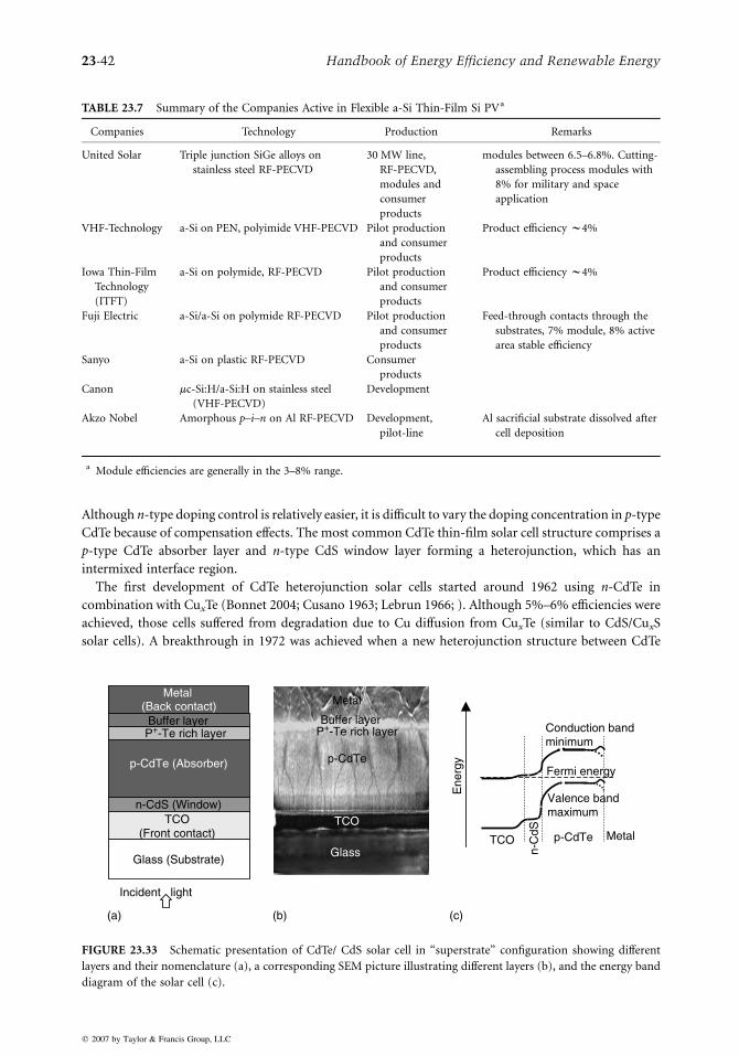
TABLE 23.7 Summary of the Companies Active in Flexible a-Si Thin-Film Si PVa
Companies Technology Production Remarks
United Solar Triple junction SiGe alloys on
stainless steel RF-PECVD
30 MW line,
RF-PECVD,
modules and
consumer
products
modules between 6.5–6.8%. Cutting-
assembling process modules with
8% for military and space
application
VHF-Technology a-Si on PEN, polyimide VHF-PECVD Pilot production
and consumer
products
Product efficiency w4%
Iowa Thin-Film
Technology
(ITFT)
a-Si on polymide, RF-PECVD Pilot production
and consumer
products
Product efficiency w4%
Fuji Electric a-Si/a-Si on polymide RF-PECVD Pilot production
and consumer
products
Feed-through contacts through the
substrates, 7% module, 8% active
area stable efficiency
Sanyo a-Si on plastic RF-PECVD Consumer
products
Canon mc-Si:H/a-Si:H on stainless steel
(VHF-PECVD)
Development
Akzo Nobel Amorphous p–i–n on Al RF-PECVD Development,
pilot-line
Al sacrificial substrate dissolved after
cell deposition
a Module efficiencies are generally in the 3–8% range.
23-42 Handbook of Energy Efficiency and Renewable Energy
Although n-type doping control is relatively easier, it is difficult to vary the doping concentration in p-type
CdTe because of compensation effects. The most common CdTe thin-film solar cell structure comprises a
p-type CdTe absorber layer and n-type CdS window layer forming a heterojunction, which has an
intermixed interface region.
The first development of CdTe heterojunction solar cells started around 1962 using n-CdTe in
combination with CuxTe (Bonnet 2004; Cusano 1963; Lebrun 1966; ). Although 5%–6% efficiencies were
achieved, those cells suffered from degradation due to Cu diffusion from CuxTe (similar to CdS/CuxS
solar cells). A breakthrough in 1972 was achieved when a new heterojunction structure between CdTe
Metal
Incident light
Glass (Substrate)
TCO(Front contact)
n-CdS (Window)
p-CdTe (Absorber)
P+-Te rich layerBuffer layer
Metal(Back contact)
TCO
n-C
dS p-CdTe
Conduction bandminimum
Fermi energy
Valence bandmaximum
Ene
rgy
(c)(b)(a)
Glass
TCO
p-CdTe
Buffer layerP+-Te rich layer
Metal
FIGURE 23.33 Schematic presentation of CdTe/ CdS solar cell in “superstrate” configuration showing different
layers and their nomenclature (a), a corresponding SEM picture illustrating different layers (b), and the energy band
diagram of the solar cell (c).
q 2007 by Taylor & Francis Group, LLC

Photovoltaics Fundamentals, Technology and Application 23-43
and CdS was developed by Bonnet and Rabenhorst (1972) and 6% efficiency was reported. Current CdTe
solar cell structures are based on this device configuration as shown in Figure 23.33 (the details of this
device structure are discussed later in the section 23.2.3.2), meanwhile, significant progress in CdTe
devices has resulted in an efficiency rise up to 16.5% (Wu et al. 2001). Historical developments of CdTe
PV technology have been reviewed by McCandless and Sites (2003).
The most attractive features of the CdTe compound are its chemical simplicity and robust stability.
Because of its highly ionic nature, the surfaces and grain boundaries tend to passivate and are not
detrimental (this is why polycrystalline CdTe solar cells are more efficient than their single-crystal
counterparts). CdTe material is inherently stable under the solar spectrum because its bonding strength,
w5.7 eV, is much higher than the incident photon energy of the solar spectrum. This accounts for the
excellent material stability and device performance. CdTe is not only stable for terrestrial applications;
recent work has demonstrated the excellent stability of CdTe, superior to Si, GaAs, CIGS etc., under high-
energy photon and electron irradiation for space applications (Batzner et al. 2004).
Table 23.5 lists the efficiency of the CdTe solar cells reported by laboratories and prominent
manufacturers. An efficiency of 16.5% has been reported by NREL USA (Wu et al. 2001) for an
approximate area of 1 cm2, whereas cell efficiencies of more than 12% are reported by several groups
using different deposition methods and substrates. The theoretical efficiency of CdTe solar cell is
estimated to be w29%, (Jsc w30 mA/cmK2 and Voc w1.0 V) which is higher than c-Si. There is therefore
plenty of room for improvement in the conversion efficiency in the future. However, similar to other
thin-film PV technologies, current CdTe technology also suffers from some problems, namely
reproducibility of the device performance when small-area cells are scaled to a larger area. Other
important issues are formation of good ohmic contacts on p-CdTe, and reduction of optical absorption
losses from the CdS and TCO front-contact layers. These are some inherent critical issues requiring
further investigation to achieve greater than 20% cell efficiency with single-junction devices. Progress of
CdTe technology has also been hampered because of environmental concerns due to cadmium; these
issues are addressed in Section 23.2.5.
23.2.3.2 CdTe Solar Cell Device Structure
The CdTe solar cells can be grown in both substrate and superstrate configurations. However, the highest
efficiencies have been achieved in the superstrate configuration. Figure 23.33a gives the schematics of a
CdTe solar cell grown on a TCO-coated glass substrate in a superstrate configuration. The glass substrate
can be a low-cost soda-lime glass for processing temperatures below 5008C, or alkali-free glass (generally
borosilicate) for high-temperature processing above 5008C. Substrate configuration would require CdTe
to be deposited on metal foils or metal-deposited glass substrates. However, stability of the back contact,
in particular, is a limiting factor in this configuration because CdTe/ CdS layers need to be grown at such
high temperatures that interdiffusion degrades the CdTe back contact interface and cells are shunted.
Therefore, substrate configuration is not actively pursued in CdTe solar cells (Figure 23.34).
In the superstrate configuration, layers of TCO, CdS, CdTe, and the metal back contact are sequentially
grown on glass substrates. There are some intermediate processing steps that will be described later. An
antireflection coating on the glass rear surface is often applied to reduce the reflection at the air-glass
interface. The incident light passes through the glass, TCO, and CdS and gets absorbed in the CdTe layer,
where it creates electron-hole pairs that contribute to the photovoltaic power.
TCO Front Electrical Contact. A highly transparent and n-type conducting TCO layer with an electron
affinity below 4.5 eV is required to form an ohmic contact and to have good band alignment with n-CdS.
Most of the TCOs, such as SnOx:F, ITO, ZnO:Al, and Cd2SnO4 (cadmium stannate), have been used to
grow high-efficiency (greater than 12%) solar cells, but the highest efficiency (16.5%) cells have been
achieved on a bilayer stack of highly resistive Zn2SnO4 on conductive Cd2SnO4 by Wu et al. (2001). Though
a single layer of TCO provides high-efficiency cells, a bilayer (combination of high and low resistive TCO
stack) is often used to protect against shunts caused by pinholes in thin CdS layers. The most commonly
used TCO in industrial production is SnOx:F, and often with a thin ITO layer. ITO front contacts are often
q 2007 by Taylor & Francis Group, LLC
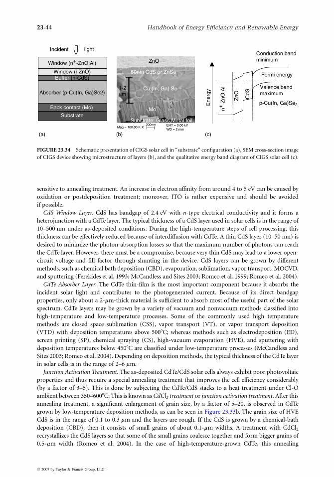
Incident light
Substrate: Glass,Metal foil,
50nm CdS or ZnSe
ZnO
Mo
1-2µm
Cu (In, Ga) Se
Substrate
Back contact (Mo)
Absorber (p-Cu(In, Ga)Se2)
Buffer (n-CdS)Window (i-ZnO)
Window (n+-ZnO:Al)
Ene
rgy
Conduction bandminimum
n+-Z
nO:A
l
CdS
p-Cu(In, Ga)Se2
(c)(b)(a)
Fermi energy
ZnO
Valence bandmaximum
Mag = 100.00 K X200nm EHT = 3.00 kV
WD = 2 mm
FIGURE 23.34 Schematic presentation of CIGS solar cell in “substrate” configuration (a), SEM cross-section image
of CIGS device showing microstructure of layers (b), and the qualitative energy band diagram of CIGS solar cell (c).
23-44 Handbook of Energy Efficiency and Renewable Energy
sensitive to annealing treatment. An increase in electron affinity from around 4 to 5 eV can be caused by
oxidation or postdeposition treatment; moreover, ITO is rather expensive and should be avoided
if possible.
CdS Window Layer. CdS has bandgap of 2.4 eV with n-type electrical conductivity and it forms a
heterojunction with a CdTe layer. The typical thickness of a CdS layer used in solar cells is in the range of
10–500 nm under as-deposited conditions. During the high-temperature steps of cell processing, this
thickness can be effectively reduced because of interdiffusion with CdTe. A thin CdS layer (10–50 nm) is
desired to minimize the photon-absorption losses so that the maximum number of photons can reach
the CdTe layer. However, there must be a compromise, because very thin CdS may lead to a lower open-
circuit voltage and fill factor through shunting in the device. CdS layers can be grown by different
methods, such as chemical bath deposition (CBD), evaporation, sublimation, vapor transport, MOCVD,
and sputtering (Ferekides et al. 1993; McCandless and Sites 2003; Romeo et al. 1999; Romeo et al. 2004).
CdTe Absorber Layer. The CdTe thin-film is the most important component because it absorbs the
incident solar light and contributes to the photogenerated current. Because of its direct bandgap
properties, only about a 2-mm-thick material is sufficient to absorb most of the useful part of the solar
spectrum. CdTe layers may be grown by a variety of vacuum and nonvacuum methods classified into
high-temperature and low-temperature processes. Some of the commonly used high temperature
methods are closed space sublimation (CSS), vapor transport (VT), or vapor transport deposition
(VTD) with deposition temperatures above 5008C; whereas methods such as electrodeposition (ED),
screen printing (SP), chemical spraying (CS), high-vacuum evaporation (HVE), and sputtering with
deposition temperatures below 4508C are classified under low-temperature processes (McCandless and
Sites 2003; Romeo et al. 2004). Depending on deposition methods, the typical thickness of the CdTe layer
in solar cells is in the range of 2–6 mm.
Junction Activation Treatment. The as-deposited CdTe/CdS solar cells always exhibit poor photovoltaic
properties and thus require a special annealing treatment that improves the cell efficiency considerably
(by a factor of 3–5). This is done by subjecting the CdTe/CdS stacks to a heat treatment under Cl-O
ambient between 350–6008C. This is known as CdCl2 treatment or junction activation treatment. After this
annealing treatment, a significant enlargement of grain size, by a factor of 5–20, is observed in CdTe
grown by low-temperature deposition methods, as can be seen in Figure 23.33b. The grain size of HVE
CdS is in the range of 0.1 to 0.3 mm and the layers are rough. If the CdS is grown by a chemical-bath
deposition (CBD), then it consists of small grains of about 0.1-mm widths. A treatment with CdCl2recrystallizes the CdS layers so that some of the small grains coalesce together and form bigger grains of
0.5-mm width (Romeo et al. 2004). In the case of high-temperature-grown CdTe, this annealing
q 2007 by Taylor & Francis Group, LLC
Photovoltaics Fundamentals, Technology and Application 23-45
treatment recrystallization is observed, but the grain size near the top surface does not increase because
the grains are already a few microns large even in the as-deposited condition.
For high-temperature growth processes, there is a tendency of CdSxTe1–x formation by the conversion of
small CdS grains into CdTe due to interdiffusion at the interface, and little or low grain growth is noticed
after the activation treatment. A stable CdS/CdTe interface can be obtained for 6% diffusion of sulfur
atoms. However, under nonequilibrium conditions, the diffusion of S decreases the thickness of the CdS
films, causing pinholes and eventually leading to shorting paths across the junction. This is a critical
problem in CdTe solar cells that restricts the application of thinner CdS as desired to minimize the optical-
absorption losses. Nevertheless, a thermal treatment of a CdS layer prior to CdTe deposition is frequently
applied to restrict the interdiffusion of S. The formation of CdSxTe1–x after activation actually helps in
reducing the lattice mismatch between CdS and CdTe, but only marginally as compared to improvements
in electrical changes induced by Cl, O, and S. Apart from the reduction in density of stacking faults and
misfit dislocation, there is an overall increase in the shallow-acceptor concentration in CdTe, leading to
enhanced p-doping in CdTe after annealing. In particular, the grain-boundary regions become more
p-doped, owing to preferred grain boundary diffusion and segregation of Cl and O. As a result, increased
charge-carrier collection efficiency is measured and efficiency increases by a factor of 3–5.
Problems of Electrical Back Contact and Stability. An important issue in CdTe solar-cell technology is
the formation of efficient and stable ohmic contacts on p-CdTe layers. For an ohmic contact to form on a
p-type semiconductor, the work function of the metal should be higher than the sum of the bandgap and
the electron affinity of the semiconductor, otherwise a Schottky contact is formed. For a p-CdTe layer, a
metal with a work function higher than 5.7 eV is needed because CdTe has a bandgap of 1.45 eV and
electron affinity is 4.3 eV. Metals with such high work functions are not available. To overcome this
problem, a heavily doped p-CdTe surface is created with the help of chemical etching and a buffer layer of
high carrier concentration is often applied. Subsequent postdeposition annealing diffuses some buffer
material into CdTe, where it changes the band edges as a result of a change in the interface state density. A
lowering in interface barrier height and width results that enables a quasi-ohmic or tunnelling contact
between the metal and CdTe, as shown in Figure 23.33c. Commonly used buffer layer/metallization
combinations are Cu/Au, Cu/graphite, or graphite pastes doped with Hg and Cu. However, back contacts
containing Cu in any form are often not stable with time, as Cu migration from the back contact leads to
efficiency degradation. However, alternate processes are being developed. Among them Sb2Te3/Mo and
Sb/Mo contacts have provided high efficiency and long-term stable solar cells (Abken and Bartelt 2002;
Batzner et al. 2001; Batzner et al. 2004; Romeo et al. 2004).
23.2.3.3 Deposition Techniques
The CdTe deposition process and substrate temperature have strong influence on the microstructure of
CdTe layer and solar cell efficiency. Low-temperature processes (less than 4508C) yield lower efficiency
(maximum is 14.5%), whereas high-temperature (500–6008C) processes yield 15–16.5% efficiency cells.
HVE is a simple deposition method where CdTe and CdS are congruently evaporated from
crucibles/boats on substrates at 1508C for CdS and w3008C for CdTe. In this process, the layers are
grown in a high vacuum (w10K5 torr), but the distance between the source material and substrate is
kept in the range of 10–30 cm. This allows the use of substrates at relatively lower temperature. Typical
deposition rates vary between 2–10 mm/h. Solar cells of approximately 12–13% efficiency have been
achieved by Stanford University, USA, ETH Zurich, Switzerland, and IEC, USA (Fahrenbruch et al. 1992;
McCandless et al. 1999; Romeo et al. 2004).
Sputtering is another process that involves a vacuum system with ionized gases forming plasma
discharge, where a CdTe target (a few-mm-thick plate) attached to one electrode is used as the source
material. The energetic ionized atoms from the plasma strike the target and remove the material atoms;
consequently a CdTe layer is deposited on the substrate, which is placed on the counter electrode facing
the target. Sputtering methods are suitable for large-area deposition in an industrial environment.
However, because of the difficulty in maintaining stoichiometry, they are considered unsuitable for
q 2007 by Taylor & Francis Group, LLC

23-46 Handbook of Energy Efficiency and Renewable Energy
compound semiconductors. However, 14% efficiency has been recently achieved with this process at the
University of Toledo, USA (Compaan et al. 2004), which is a very encouraging result.
CSS and VT are the prominent industrial processes used for CdTe deposition owing to their very high
rate (2–5 mm/min) of deposition. The CSS process consists of an arrangement involving the placement of
a graphite crucible with the source material (CdTe compound) in a high-vacuum chamber (w10K
5 torr). The CdTe compound sublimes at around 6008C and is deposited onto the substrate, which is kept
with a separation of 1 to 5 mm above the crucible and heated typically above 5508C. Antec Solar GmbH
in Germany uses this method for industrial production of 60 ! 120 cm2 modules on a 10 MW capacity
plant. Parma University, Italy, University of South Florida, USA and NREL, USA have also used this
method and cells of 15.5% to 16.5% efficiency have been achieved. First Solar, USA uses a variant of
CSVT, where instead of a compound, elemental vapors are used (Romeo et al. 2004; McCandless and
Dobson 2004; First Solar 2005). First Solar is the most successful CdTe company to date, as they upscale
the production from w15 MW to 75 MW modules on 60 ! 120 cm2 glass substrates.
Details of other alternative methods such as screen printing, spray pyrolysis, MOCVD, CVD, atomic
layer deposition (ALD), and electrodeposition (ED) may be found in the literature (Bonnet and
Rabenhorst 1972; Romeo et al. 2004). For flexible substrates such as polymers, low-temperature
methods such as sputtering, HVE, and electrodeposition (ED) are suitable.
23.2.3.4 Flexible CdTe Solar Cells
Even though the technology of CdTe solar cells on glass substrates has matured and efficiencies exceeding
16% have been achieved, not much effort has been placed into developing these devices on flexible
substrates. The R&D on flexible CdTe has been supported by NASA and defense agencies in the US.
Because of high radiation tolerance (superior to conventional Si and GaAS solar cells) against high-
energy electron and proton irradiation, these solar cells are also attractive for space applications in
addition to terrestrial applications.
Although the CdTe solar cells can be grown in “substrate” configuration, one of the hurdles in the
development of high-efficiency CdTe solar cells on metallic substrates is that most of the metal foils do
not form efficient ohmic contact with CdTe and it is difficult to incorporate an additional buffer layer as
an ohmic contact to increase the cell efficiency. The criteria of matching thermal expansion coefficients
and work function limit the choice of available substrate materials. Another reason is that during CdCl2annealing treatment, diffusion of impurities changes the ohmic-contact properties. Flexible solar cells of
up to 8% efficiency have been achieved on metal foils.
The choice of an appropriate substrate is a crucial factor for flexible solar cells in the superstrate
configuration because the substrate should be optically transparent and should withstand the high
processing temperatures. Most of the CdTe/CdS cell fabrication techniques require temperatures in the
range 450–5008C. Therefore, low-temperature (less than 4508C) deposition processes are required.
However, recently, ETH in Zurich, Switzerland has reported 11.4%-efficiency flexible cells on polymer
foil and demonstrated the first monolithically interconnected mini-modules. These devices were grown
with the HVE method, which is suitable for roll-to-roll deposition, but the concept for industrial
production has yet to be demonstrated (Mathew et al. 2004; Romeo et al. 2004). The 11.4% efficiency of
single-junction CdTe compares well with the 12% (initial, prior to degradation) best efficiency of triple-
junction a-Si solar cells.
23.2.4 Cu(In Ga)Se2 Solar Cells
23.2.4.1 Material and Properties
Compound semiconductors from the I–III–VI2 series of the periodic table, such as copper-indium-
diselenide (CIS), copper-gallium-diselenide (CGS), and their mixed alloys copper-indium-gallium-
diselenide (CIGS) are often simply referred to as chalcopyrites because of their tetragonal crystal
structure. These materials are easily prepared in a wide range of compositions and their corresponding
phase diagrams have been intensively investigated. Changing the stoichiometry and extrinsic doping can
q 2007 by Taylor & Francis Group, LLC

Photovoltaics Fundamentals, Technology and Application 23-47
vary their electrical conductivity. However, for the preparation of solar cells, only slightly Cu-deficient
compositions of p-type conductivity are suitable. Depending on the [Ga] / [In C Ga] ratio, the bandgap
of CIGS can be varied continuously between 1.04 and 1.68 eV. The current high-efficiency devices are
prepared with bandgaps in the range of 1.20–1.25 eV; this corresponds to a [Ga] / [In C Ga] ratio
between 20% and 30%. Layers with higher Ga content, as needed to increase the bandgap towards
w1.5 eV, are of inferior electronic quality and yield lower-efficiency cells.
Other chalcopyrites such as CuInS2 and CuInTe2 were also investigated, but cell efficiencies were rather
low and the R&D focus was placed on CIS. Recently, interest in CuInS2 has resurfaced with the
development of w11.4% efficient cells at HMI Berlin. A spin-off company, Sulfurcell, also based in
Berlin, started setting up a pilot production line in 2003. The device structure of the CuInS2 solar cell is
quite similar to CIGS solar cells in terms of other constituent layers.
The first CIS solar cell was developed with single-crystal material and w12% efficiency was reported in
1974 (Wagner et al. 1974). The first thin-film CIS solar cell was reported by Kazmerski in 1976 by
developing w4% cells obtained with the evaporation of CuInSe2 material (Kazmerski et al. 1976). The
real breakthrough in CIS thin-film technology came with the pioneering work of the Boeing Corp., USA,
where they used three-source evaporation of Cu, In, and Se elements and raised the efficiency from 5.7%
in 1980 to above 10% in 1982 (Mickelsen and Chen 1981; Mickelsen and Chen 1982). This success,
despite the apparent complexity of the material system, clearly showed the promising potential of the
material. Later, in 1987, Arco Solar, USA, raised the cell efficiency to w14% by using a different CIS
deposition process where a stacked metal layer was selenized under H2Se ambient (Mitchell et al. 1988).
Subsequent improvements in efficiency were attained by the EUROCIS consortium in Europe and later at
NREL, USA, which holds the efficiency record of w19.5%, the highest for any thin-film, single-
junction solar cells (Ramanathan et al. 2003). Efficiency improvements over the Boeing process occurred
due to addition of Ga and S for bandgap engineering, the addition of Na in the absorber layer,
optimization of the n-CdS (heterojunction part of the cell), and transparent front electrical
contact layers.
The first industrial production of CIS modules was started by the Siemens (later Shell Solar) based on
the Arco solar technology, whereas other companies such as Wurth Solar and Global Solar started
development of CIS solar modules using coevaporation methods. Several other companies have
been investigating various other methods of deposition, such as paste printing, electrodeposition, etc.,
but up to now these technologies have been less successful as compared to vacuum-based technologies.
The phase diagram of the ternary compound is described by the pseudo-binary phase diagram of the
binary analogue, e.g., Cu2Se and In2Se3 phase for CuInSe2 ternary. Single-phase chalcopyrite CuInSe2
exists at small copper deficiency, whereas for Cu-rich compositions, a mixed phase of CuxSe with CuInSe2
forms that is not suitable for PV devices. For In-rich compositions, the defect-chalcopyrite phase
(CuIn3Se5) forms, that is generally n-type. Despite an apparent complicated crystal structure and
multicomponent system, the material properties of the PV-relevant compounds are fault-tolerant and
not particularly affected by minor deviations from stoichiometry in the Cu-deficient range. Further,
surfaces and grain boundaries in CIGS compounds are easy to passivate, resulting in high-efficiency cells
even with submicron grain-size materials.
The PV-grade Cu-deficient CIGS material has a tetragonal crystal structure having vacancies and
interstitials that act favorably, especially because the material is self-healing, owing to the defect
relaxation caused by highly mobile Cu ions and its interaction with vacancies. Defects created in
CIGS by external influence (e.g., radiation) are immediately healed. This is an inherent advantage of the
CIGS material, leading to highly stable CIGS solar cells. However, care must be taken for proper
encapsulation of devices against highly damped conditions, otherwise the degradation of electrical
contacts (TCO or Mo) in moisture can lead to minor degradations in performance. Therefore, stability of
encapsulated CIGS solar cells is not a problem, as proven by field tests conducted by ZSW, Shell, and
NREL. CIGS is also tolerant against space radiation, being superior to Si and GaAs single-crystal cells, but
somewhat inferior to CdTe.
q 2007 by Taylor & Francis Group, LLC

23-48 Handbook of Energy Efficiency and Renewable Energy
23.2.4.2 CIGS Solar-Cell Configuration
The CIGS solar cells can be grown in both substrate and superstrate configurations, but the substrate
configuration gives the highest efficiency due to favorable processing conditions (Figure 23.34). However,
it requires an additional encapsulation layer and/or glass to protect the cell surface, which is not required
in the superstrate configuration. Superstrate structures were investigated in the early 1980s, but efficiency
was below 5%. However, recent efforts have improved the efficiency to w13%. This has been possible
with the introduction of undoped ZnO instead of CdS as a buffer layer, and coevaporation of NaxSe
during the CIGS deposition. Furthermore, the developments in bifacial CIGS solar cells with both front
and rear transparent conducting contacts, is making sound progress (Nakada et al. 2004).
Electrical Back Contact. CIGS solar cells in substrate configuration can be grown on glass as well as
metal and polymer foils. Molybdenum (Mo), grown by sputtering or e-beam evaporation is the most
commonly used electrical back contact material for CIGS solar cells. Growth of the solar cell starts with
the deposition of Mo on the substrate, which forms an electrically conducting back electrode with CIGS.
When CIGS is grown on Mo, an interface layer of MoSe2 is automatically formed that helps in ohmic
transport between CIGS and Mo. Recently, alternative back contact materials have been explored, but
industrial production is still based on Mo layers.
CIGS Absorber Layer. Because of a high absorption coefficient, a 2-mm-thick layer is sufficient for
absorption of maximum incident radiation. CIGS layers can be grown with a variety of deposition
methods (as described later). Although the grain size and morphology (surface roughness) depend on
deposition methods, efficiencies greater than 13% have been achieved with most of the methods, which
indicates that grain boundaries in CIGS are benign and can be easily passivated. High-efficiency cells have
p-type Cu(In,Ga)Se2 bulk, while a defect-chalcopyrite Cu(In,Ga)3Se5 phase in the form of a thin layer
segregates at the top surface that is n-type, especially when doped by cation atoms diffusing from the
buffer layer. It is believed that this inverted surface, leading to a p–n homojunction in the CIGS absorber,
is crucial for high-efficiency cells.
Buffer Layer. Several semiconductor compounds with n-type conductivity and bandgaps between 2.0
and 3.4 eV have been applied as a buffer to form a heterojunction in CIGS solar cells. However, CdS
remains the most widely investigated buffer layer because it has continuously yielded high-efficiency cells
on different types of absorber layers. CdS for highest-efficiency CIGS cells is commonly grown by
chemical-bath deposition (CBD), which is a low-cost, large-area process. However, its incompatibility
with in-line vacuum-based production methods is a matter of concern. Although CBD-grown CdS serves
as a reference for the highest efficiency, physical vapor deposition (PVD)-grown CdS layers yield lower-
efficiency cells. Thin layers grown by PVD often do not show uniform coverage of CIGS and are less
effective in chemically engineering the interface properties between the buffer and the absorber. The
recent trend in buffer layers is to substitute CdS with Cd-free wide-bandgap semiconductors and to
replace the CBD technique with in-line-compatible processes. Alternative materials such as In2S3, ZnO,
ZnS, ZnSe, etc., using different methods such as PVD, RF sputtering, metal organic chemical vapor
deposition (MOCVD), atomic layer deposition (ALD), or a novel technique called ion layer gas reaction
(ILGAR), are being explored (Bhattacharya and Ramanathan 2004; Chaisitsak et al. 2001; Ohtake et al.
1995; Olsen et al. 2002; Spiering et al. 2003). A record efficiency of 18.8% has recently been achieved with
for CBD-ZnS (Nakada and Mizutani 2002). Most industries are currently using CBD-CdS but Showa
Shell has shown 14.2% efficiency on 864 cm2 submodule developed with CBD-grown ZnS(O,OH) buffer
layers (Kushiya, 2004).
Front Electrical Contact. TCOs with bandgaps of above 3 eV are the most appropriate and have become
the ultimate choice for front-contact due to their excellent optical transparency (greater than 85%) and
reasonably good electrical conductivity. Today, CIGS solar cells employ either ITO or, more frequently,
RF-sputtered Al-doped ZnO. A combination of an intrinsic and a doped ZnO layer is commonly used.
Although this double layer yields consistently higher efficiencies, the beneficial effect of intrinsic ZnO is
still under discussion. Doping of the conducting ZnO layer is achieved by group-III elements, particularly
with aluminum. However, investigations show boron to be a feasible alternative because it yields a high
q 2007 by Taylor & Francis Group, LLC

Photovoltaics Fundamentals, Technology and Application 23-49
mobility of charge carriers and a higher transmission in the long-wavelength spectral region, giving rise
to higher currents. For high-efficiency cells, the TCO deposition temperature should be lower than 1508C
to avoid the detrimental interdiffusion across CdS/CIGS interface. RF sputtering is not considered
suitable for industrial production; therefore, alternative sputtering and CVD methods are investigated
and used.
Sodium Incorporation into CIGS. One of the breakthroughs in CIGS PV technology occurred when the
alumina or borosilicate glass substrate was replaced by soda-lime glass to match the thermal expansion
coefficients, which resulted in substantial efficiency improvement (Hedstrom et al. 1993). It was
subsequently realized that sodium (Na) plays an important role in high-efficiency CIGS solar cells
because it affects the microstructure (grain size), and passivates the grain boundaries, leading to changes
in electronic conductivity by up to two orders of magnitude. The overall effect is efficiency improvement
primarily because of an increase in the open-circuit voltage (Voc) and fill factor (FF) of the solar cells.
Most commonly, Na is introduced into CIGS by diffusion from the soda-lime glass substrate during the
absorber deposition. However, sodium incorporation from such an approach is neither controllable nor
reliable; therefore, alternative methods to add Na from external sources are used either during or after the
deposition of CIGS layers. These methods include the coevaporation or the deposition of a thin
precursor of a Na compound such as NaF, Na2Se, or Na2S for CIGS on Na-free substrates that include
soda-lime glass covered with barrier layers (Al2O3, Si3N4, etc., as used by Shell Solar). These barrier layers
inhibit sodium diffusion from the glass substrate. CIGS on flexible substrates (metal and polyimide foils)
also need controlled incorporation of sodium, which is provided from a precursor layer applied prior to
or after the CIGS growth.
23.2.4.3 Deposition and Growth of CIGS Absorber
There are number of processes used for the deposition of the CIGS thin-films, some of them are briefly
described:
Coevaporation Processes. As described earlier, vacuum evaporation is the most successful technique for
deposition of CIGS absorber layers for highest-efficiency cells. The vacuum evaporation method involves
simultaneous evaporation of the constituent elements from multiple sources in single or sequential
processes during the whole absorber deposition process. While a variation of the In to Ga ratio during the
deposition process leads to only minor changes in the growth kinetics, the variation of the Cu content
strongly affects the film growth. Thus, different coevaporation growth procedures are classified by their
Cu evaporation profile (Figure 23.35).
One variant of coevaporation is a bilayer process (also called the Boeing process), which originates from
the work of Mickelsen and Chen (McCandless and Dobson 2004) and yields larger grain sizes compared
to the constant-rate (single-stage) process. This is attributed to the formation of a CuxSe phase during the
Cu-rich first stage that improves the mobility of group-III atoms during growth.
The highest efficiencies in laboratories are achieved with the so-called three-stage process, introduced by
NREL, (Gabor et al. 1994). With this process, the CIGS layer is obtained by starting the deposition of an
(In,Ga)xSey precursor, followed by the codeposition of Cu and Se until a Cu-rich overall composition is
reached, and finally the overall Cu concentration is readjusted by subsequent deposition of In, Ga, and Se.
CIGS films prepared by the three-stage process exhibit a large-grained, smooth surface, that reduces the
junction area and is thereby expected to reduce the number of defects at the junction and yield high
efficiency. Several groups have developed 16–19.5% efficiency cells using CIGS grown with the three-
stage process.
Selenization of Precursor Materials. The selenization of precursors is another method of obtaining CIGS
thin-films. This sequential process is favorable due to its suitability for large-area film deposition with
good control of the composition and film thickness following the initial success of Arco Solar in 1987.
Such processes consist of the deposition of a precursor material obtained by sputtering, evaporation,
electrodeposition, paste printing, spray pyrolysis, etc., followed by thermal annealing in controlled
reactive or inert atmosphere for optimum compound formation via the chalcogenization reaction as
illustrated below in Figure 23.36. The precursor materials are either stacked metal layers or a
q 2007 by Taylor & Francis Group, LLC

Constant rates
Deposition time Deposition time Deposition time
Bilayer/ Boeing process 3-stage process
Se
In+GaCuE
vapo
ratio
n ra
tes
subs
trat
e te
mpe
ratu
re
Eva
pora
tion
rate
ssu
bstr
ate
tem
pera
ture
Eva
pora
tion
rate
ssu
bstr
ate
tem
pera
ture
Substrate
Se
In+Ga
Cu
Substrate
Se
In+Ga
Cu
1st stage 2nd stage 3rd stage
Substrate
FIGURE 23.35 Diagram representing the recipes in the co-evaporation processing steps in the deposition of
Cu(In,Ga)Se2 used for constant rate, bilayer or Boeing, and three-stage process. (From Romeo, A., Terheggen, M.,
Abou-Ras, D., Batzner, D. L., Haug, F.-J., Kalin, M., Rudmann, D., and Tiwari, A. N., Prog. in Photovolt: Res. App., 12,
93–111.)
23-50 Handbook of Energy Efficiency and Renewable Energy
stack of their compounds and alloys. Shell Solar, USA and Showa Shell, Japan use sputtering techniques
for precursor deposition and production of large-area solar modules up to 60 ! 120 cm2, yielding
maximum efficiencies of 13% on 30 ! 30 cm2 modules (Karg 2001; Kushiya et al. 2003; Palm et al. 2004).
Solar modules produced by Shell Solar, USA are commercially available in the market.
Alternative CIGS Growth Processes. There is substantial interest in using nonvacuum methods for
CIGS deposition. An innovative approach utilizes the stability of the oxides to produce nanosized
precursor particles (Eberspacher et al. 2001; Kapur et al. 2001; Kaelin et al. 2004). Nanosized metal oxides
Precursor deposition(low substrate temperature)
Selenization/Annealing/Recrystallization(high substrate temperature 450−600°C)
Methods
Sputtering
Vac
uum
met
hods
Non
-vac
uum
met
hods
Cu, In, GaStacked elemetallayers, alloys of
compoundswith or without
selenium
Cu, In, Ga, Se/Scompounds
Cu, In, Ga, Ocompounds
Small grained, alloyed or stacked layerwith defined metal ratios
Evaporation
Electrodeposition
Spray pyrolysis
Paste coating
Glass substrateMolybdenum
Glass substrateMolybdenum
Materials Pretreatment Selenization
Selenization reactionSe/S, H2Se/S gas ambient
Selenization reactionSe/S, H2Se/S gas ambient
RecrystallizationSe/S, H2Se/S gas ambient
Optionalpurification
by H2 annealing
Binder eliminationH2 reduction to metal alloy
Polycrystalline CIGS layer
FIGURE 23.36 Schematic of the various processes for selenization of precursor materials. (From Romeo, A.,
Terheggen, M., Abou-Ras, D., Batzner, D. L., Haug, F.-J., Kalin, M., Rudmann, D., and Tiwari, A. N., Prog. in
Photovolt: Res. App., 12, 93–111.)
q 2007 by Taylor & Francis Group, LLC

Photovoltaics Fundamentals, Technology and Application 23-51
are mixed in an ink suspension that allows low-cost, large-area deposition by doctor blading, screen
printing, or spraying of the precursor. Such nonvacuum deposition of precursors allows a very efficient
material utilization of almost 100% of the nonabundant metals indium and gallium. A selenization
treatment converts the precursor into a CIGS layer and solar-cell efficiencies of over 13% have been
achieved by ISET, USA. One of the drawbacks of the process is the toxicity of the H2Se gas used for
selenization. However, recent efforts are being made to selenize printed precursors with Se vapors (Kaelin
et al. 2004).
The CIGS compound can also be formed directly by electrodeposition from a chemical bath (Hodes
et al. 1986). Several groups, including EDF-CNRS, France, CIS Solar Technologies, Germany, and
CISCuT, Germany, have been using such approaches and have obtained cells with efficiencies greater than
10%. With a hybrid approach that uses additional vacuum deposition on an electrodeposited precursor
layer, efficiencies as high as 15.4% have been achieved at NREL, USA.
23.2.4.4 Flexible CIGS Solar Cells
Probably the ultimate advantage of thin-film technology is the application of roll-to-roll manu-
facturing for production of monolithically interconnected solar modules leading to low energy
payback time because of high-throughput processing and low cost of the overall system. A large
number of activities on highly efficient, stable, and flexible thin-film modules based on CIGS has
recently drawn much interest for flexible solar cells on metal and plastic foils. Apart from the
expected high efficiency and long-term stability for terrestrial applications, flexible CIGS has excellent
potential for space application because of its space-radiation-tolerant properties that are 2–4 times
superior to the conventional Si and GaAs cells. Lightweight and rollable solar array structures will not
only reduce the overall cost of space-deployable solar modules, but also can substantially save on the
launching cost of satellites.
Development and current status of flexible CIGS solar cells have been reviewed by Kessler and
Rudmann (2004). Flexible CIGS cells can be grown on polyimide and on a variety of metals, e.g.,
stainless steel (SS), Mo, Ti, etc. Therefore, the choice of substrate is important because there are some
advantages and disadvantages: (1) the density of usable metals is 4–8 times higher than that of
polymers; therefore, cells on metals are heavier; (2) metals are conducting and have rough surfaces;
therefore, monolithic module development is difficult, which, in contrast, is easier on polymer foils;
(3) stainless steel foils need an extra barrier layer against detrimental impurity (e.g., Fe) diffusion of
the metal into the CIGS during deposition; (4) metal foils can withstand high deposition
temperatures (5508C–6008C), which leads to higher efficiency than that achieved with polymer
foils that are not suitable for processing temperatures greater than 4508C.
High-record efficiencies of flexible CIGS solar cells are 17.5% on stainless steel by Daystar, U.S.A.
(Tuttle et al. 2000) and 14.1% on polymer foil by ETH Zurich, Switzerland (Bremaud et al. 2005).
Several research groups and industries are involved in the development of flexible solar cells, but
Global Solar, U.S.A. is the only company manufacturing flexible CIGS on a pilot production line.
They have reported a 13.17% cell of 68.8 cm2 and modules of 11.13% (on 3898 cm2) and 10.10% (on
7085 cm2) on metal foils (Beck et al. 2005). The solar modules on SS foils are not monolithically
connected; they are made by connecting individual cells into a large-area cell with an overlap method.
ZSW, Germany is developing a scribing and patterning method for monolithically connected solar
modules on metal and polymer foils (Kessler and Rudmann 2004). The basic schematic cross-section
of a monolithic module on glass is shown in Figure 23.37 along with a flexible prototype mini-
module developed on polymer foil by ZSW & ETH, Zurich, within a European collaborative project.
Table 23.8 gives an overview of different flexible solar cell technologies, including the organic and
dye-sensitized TiO2 based PV technologies. Because of late start in R&D, flexible CIGS and CdTe
solar cells are industrially less mature compared to a-Si cells. However, high cell efficiencies and
inherent stability advantages indicate a promising potential for these technologies.
q 2007 by Taylor & Francis Group, LLC

CIGS(2 µ m)
Mo(0,5 µ m)
(0,05 µ m)
(1 µ m)
CdS
ZnO
(a)
(b)
Glass(1−3 µ m)
FIGURE 23.37 (See color insert following page 774.) Flexible monolithic CIGS modules showing a prototype
mini-module on a polymer foil (a) and schematic cross-section of the module (image taken from the website of ZSW)
exhibiting the material component layers and their interconnect patterns (b).
23-52 Handbook of Energy Efficiency and Renewable Energy
23.2.5 Environmental Concerns and Cd Issue
The CdTe and CIGS thin-film technologies have demonstrated excellent potential for the cost-effective
production of solar electricity. However, these technologies, especially the CdTe, suffer from the perception
of toxicity of the constituent element Cd, which is used in the form of a stable compound in thin-film
modules. Often raised issues are the risks or hazards associated with the use of materials during
the processing and fabrication of CdTe/CdS and CdS/CIGS solar cells and risks associated during the
TABLE 23.8 An Overview of Different Flexible Solar Cell Technologies
CIGS CdTe Amorphous Silicon Organic & Dye Solar
Cells
Lab efficiency on
plastic foil
14.1% (Single-
junction cell)
11.4% (Single-
junction cell)
8–12%a
(multijunction
cell)
5 to 8%
Lab efficiency on
metal foil
17.5% (Single-
junction cell)
8% (Single-junction
cell)
14.6a/13%
(multijunction
cell)
7%
Industrial efficiency
(typical values)
6–11% (On steel foil,
not yet available on
plastic foil)
Not yet demonstrated 4–8%a (Available on
plastic and metal
foils
Not yet demonstrated
Stability under light Material stable Material stable Degrades Stability not proven
a Initial values measured before light-induced degradation of solar cells.
q 2007 by Taylor & Francis Group, LLC

Photovoltaics Fundamentals, Technology and Application 23-53
cradle-to-grave operating lifetime of these modules. The environmental and health hazard (E&H) issues of
CdTe solar modules have been extensively investigated by several independent agencies, including the
national laboratories in Europe and the USA. (Fthenakis et al. 1999; Fthenakis and Zweibel 2003; Fthenakis
et al. 2004). Although CdTe technology has no chance of eliminating Cd, there is some maneuverability in
CIGS technology in the elimination of a very thin (typically w50-nm) CdS buffer layer, and thus
alternative buffer layers are being successfully pursued. Initial success has already been achieved as CIGS
solar cells of 16%–18.8% efficiencies and modules of 13.4% efficiency have been developed with alternative,
Cd-free buffers (Hedstrom et al. 1993; Kushiya 2004).
Referring to the perception and concerns on Cd issues, V. Fthenakis (Senior Chemical Engineer,
Brookhaven National Laboratory) and K. Zweibel (Manager, Thin-film Partnership Program, NREL,
USA) have presented a detailed account of their studies during their presentations at the 2003 NCPV
program review meeting in the USA (Fthenakis et al. 2004) that confirmed that CdTe panels would be
almost benign with zero emission and no associated health hazards and gave a clean chit to CdTe
technology. The following points emerged out of the studies:
Cadmium is a by-product of zinc, lead, and copper mining. It constitutes only 0.25% of its main
feedstock, ZnS (sphalerite). Cadmium is released into the environment from phosphate fertilizers, burning
fuels, mining and metal-processing operations, cement production, and disposal of metal products.
Releases from disposed Cd products, including Ni-Cd batteries are minimum contributors to human
exposure because Cd is encapsulated in the sealed structures. Most human cadmium exposure comes from
ingestion, and most of that stems from the uptake of cadmium by plants, through fertilizers, sewage sludge,
manure, and atmospheric deposition. Although long-term exposure to elemental cadmium, a carcinogen,
has detrimental effect on kidneys and bones, limited data exists in toxicology. However, the CdTe
compound is more stable and less soluble than elemental Cd and is therefore likely to be less toxic.
Considering the electrolytic refinery production of CdTe powders (from Cd wastes from the zinc,
iron, and steel industries) there would be 0.001% Cd gaseous emission. This would correspond to
0.01 g/GWh, which is significantly less as compared to the perceptions and hypes created that
estimate it at 0.5 g/GWh based on other crude processes or unsubstantiated data. The only potential
hazard would be a building fire. It has also been estimated quantitatively that the maximum
temperature of a basement on fire is w9008C, which is still less than the melting point of CdTe
(10418C). Furthermore, the vapor pressure at 8008C for CdTe is w2.5 torr (0.003 atm), so this
minimizes the risks further, and once sealed between glass plates, any Cd vapor emission is unlikely.
The main conclusion of the studies was that the environmental risks associated with CdTe-based
technology are minimal. Every energy source or product may present some direct or indirect
environmental health and safety hazards, and those of CdTe should not be considered a problem. The
following conclusions can be drawn:
† Cd is produced as a by-product of Zn and can either be put to beneficial uses or discharged to
the environment posing another risk.
† CdTe in PV is much safer than other current Cd uses.
† CdTe PV uses Cd 2500 times more efficiently than Ni-Cd batteries.
† Occupational health risks are well managed.
† There is absolutely no emission of Cd during PV operation.
† A risk from fire emission is minimal.
† CdTe technology and modules are safe and do not pose significant risks.
23.2.6 Conclusions
1. The PV market is booming with a phenomenal surging growth rate. High demand for cost-
effective PV installations with more consumer-oriented choices cannot be met by the c-Si wafer
q 2007 by Taylor & Francis Group, LLC

technology and is not expected to achieve production cost targets of less than V1/W
(Figure 23.23).
2. Thin-film PV has clearly demonstrated an excellent potential for cost-effective generation of
solar electricity if modules are produced in high-capacity production plants. A mix of c-Si and
thin-film PV technologies will cater to the market needs in the near- to midterm future, followed
by the dominance of thin-film and other PV technologies in the long term.
3. Thin-film PV industries are growing fast; however, there are several issues:
a. Reducing the gap between lab efficiency and larger area industrial production efficiency. This
is achievable with the design of better equipment with in situ diagnostics. Nonavailability of a
standard deposition system for thin-film PV has been a problem; therefore, effort is needed to
develop large area equipment suitable for thin-film PV.
b. For lower cost, high-throughput and high-yield efforts are needed that require further
simplification and increased robustness of the processes and device structures.
c. Further improvements are needed in the device structure for still higher efficiencies (greater
than 25%) and enhanced material utilization (low wastage), along with thinner layers for less
material consumption if multi-giga and terawatt PV facilities are to be successful for a safer
and prosperous world.
23.3 Concentrating PV Technologies
Roland Winston, Robert McConnell, and D. Yogi Goswami
23.3.1 Introduction
The current state of solar cell development is illustrated in Figure 22.38. While single-junction silicon
solar cells dominate today’s solar industry, the rapid rise in efficiency vs. time (experience curve) of the
multijunction cells makes this a particularly attractive technology path (NREL). The high efficiency, in
comparison with single junction cells, such as silicon, is obtained by stacking several junctions in series,
electrically isolated by tunnel diodes, as explained in section 22.1. These can be qualitatively viewed as
adding the voltages of three junctions in series, while maintaining the current of a single junction.
When compared with the very best silicon cells, the efficiency gain is about 2 today, but it is getting
better with time as Figure 22.38 convincingly shows.
Under concentrated sunlight, multijunction (GaInP/GaAs/Ge) solar cells have demonstrated
efficiencies twice (39.3%) those of most silicon cells (usually 15%–21%). This means that, in sunny
areas, a multijunction concentrator system can generate almost twice as much electricity as a silicon
panel with the same area. The concentrating optics focus the light onto a small area of cells, reducing
the area of the solar cells by a factor of, typically 500–1000 times. The reduced cell area overcomes the
increased cell cost. The cell cost is diminished in importance and is replaced by cost of optics. If the
cost of the optics is comparable to the cost of the glass and support structure needed for silicon flat-
plate modules, then the cost per unit area can remain fixed while the electricity production is
essentially doubled. Thus, in high-direct insolation locations, the multijunction concentrator
technology has the potential to reduce the cost of solar electricity by about a factor of two. As a
side benefit, the cells are more efficient under concentration, provided a reasonable cell temperature
can be maintained. Clearly, the technology may be extended to four and even five junctions if efficiency
benefits justify added cost. The efficiency is a moving target; today’s triple junction cell efficiency is
nearly 40%. Thus, one may reasonably extrapolate that multijunction cells may reach 50% efficiency in
the future. Using less cell material for a given power output has attraction to cell manufacturers that are
having trouble producing sufficient material to keep up with demand. It is worth mentioning that this
technology was first developed and proven in the space program, where specific power (power/mass) is
a more important consideration than cost.
23-54 Handbook of Energy Efficiency and Renewable Energy
q 2007 by Taylor & Francis Group, LLC

RCARCARCA RCARCA
RCA
RCABoeing
Boeing
Boeing
BoeingBoeing
Solarex
Spire
Spire
Stanford
University ofLausanne
UniversitySo. Florida
University ofLausanne
UCSBCambridge
UniversityLinz
PrincetonSiemens
ECH, TheNetherlands
UC Berkeley
Photon energy
United solar
United solar
Astropower
AstropowerNREL NREL
NREL
Fraunhofer
NREL
NRELNREL
NREL
NREL/spectrolab
Spectrolab
Spectrolab
Multijunction concentrators
Crystalline Si cells
Thin-film technologies
Emerging PV
Three-junction (2-terminal, monolithic)
Single crystal
Cu(ln,Ga)Se2CdTe
Dye cell
Organic cells(various technologies)
Amorphous Si:H (stabilized)
MulticrystallineThin Si
Two-junction (2-terminal, monolithic)Spectrolab
Japanenergy
NRELNRELNREL
NREL
Euro-CIS
AMETEX
Kodak
Kodak
Kodak Solarex
No. Carolina
Westing-house
ARCO
UNSWUNSW
UNSW UNSWUNSW
UNSWGeorgia techGeorgia tech
VarianSharp
NRELCu(ln,Ga)Se2
14x concentration
Sate universityARCO
University of maine
Masushita
19750
4
8
12
16
20
Effi
cien
cy (
%)
24
28
32
36
40
44
1980 1985 1990 1995 2000 2005
Monosolar
FIGURE 23.38 World-record conversion efficiencies for various PV technologies.
Photovoltaics Fundamentals, Technology and Application 23-55
23.3.2 CPV Market Entry
In 2004, less than 1 MW of concentrator PV systems was installed, out of a total world PV market of
1200 MW. Admittedly, 1 MW does not constitute significant market entry. However, the significant
development is an increased number of projects with sizes of several hundred kilowatts (kW), creating
a market appropriate for CPV technology. Furthermore, CPV technologies are ready today for this
market opportunity with high-efficiency solar cells and well-developed hardware. However, it is the
near-term prospects for even better performance and lower-installed system costs that are leading to
real market entry during 2005 and 2006.
Amonix, Inc., of Torrance, California, spent more than 15 years developing five generations of CPV
prototypes that led to the products most recently installed in Arizona by Arizona Public Service
(Figure 23.39) and in other southwestern U.S. locations (Amonix 2005).
Similarly, Solar Systems Pty, Ltd., of Hawthorn, Australia (Solar Systems 2005), spent more than 15
years developing several generations of their CPV prototypes that led to recent installations on
aboriginal lands in Australia—part of a market served by large diesel generating plants with high
transportation costs for the diesel fuel (Figure 23.40). The company plans to install more than 5 MW in
2006. Indeed, the growth from 1 MW of CPV in 2004 to some 18 MW in 2006 legitimately constitutes
market entry for this technology.
23.3.3 Future Growth
With market entry comes the question of sustained market growth. Carlos Algora, from the Instituto
de Energia Solar, Universidad Politecnica de Madrid, published a useful cost analysis in 2004 for
concentrator PV technologies (Algora 2004). Many of the costs came from installed system costs for the
480-kW CPV project in Tenerife, but included technology improvements for production of 10 MW and
incorporated learning curve reductions for cumulative production greater than 10 MW. The analysis
q 2007 by Taylor & Francis Group, LLC

FIGURE 23.39 Several 35-kW Amonix modules installed in an Arizona Public Service power plant. The pickup
truck underneath the module gives an idea of the scale.
23-56 Handbook of Energy Efficiency and Renewable Energy
included a wide range of parameters. Concentrations ranged from 400 to 1000 suns, with cell
efficiencies ranging from 32%–40%. The presentday CPV-installed system cost was estimated at
2.34 V/W (US$3.00/W with the present exchange rate) using 32%-efficient multijunction solar cells in
today’s CPV technology with only 10 MW of product. This part of Algora’s analysis did not incorporate
the impact of a learning curve.
The lowest projected costs in Algora’s analysis was 0.69 V/W (US$0.85/W) for 40%-efficient solar
cells, 1000-sun concentration, and cumulative production of 1000 MW, using a conservative learning
curve of 17.5% that started with 10 MW of product. Although 1000 MW may seem a distant
cumulative production target for CPV, it is informative to realize that a total of about 1 MW of
multijunction production capacity already exists at Spectrolab and other space satellite solar power
providers. This 1 MW production capacity of high-efficiency multijunction solar cells corresponds to
w1000 MW of CPV plants at 1000-sun concentration.
23.3.4 Energy Payback
CPV system costs are much more sensitive to the price of steel than to the price of silicon. In this
regard, CPV systems share similar concerns with the wind industry (McConnell 2002). Other
FIGURE 23.40 Several 25-kW solar systems modules. Again, note the people in the foreground for an idea of
module scale.
q 2007 by Taylor & Francis Group, LLC
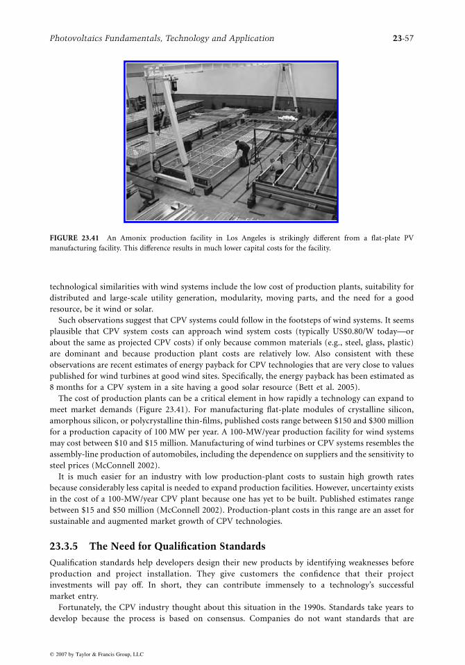
FIGURE 23.41 An Amonix production facility in Los Angeles is strikingly different from a flat-plate PV
manufacturing facility. This difference results in much lower capital costs for the facility.
Photovoltaics Fundamentals, Technology and Application 23-57
technological similarities with wind systems include the low cost of production plants, suitability for
distributed and large-scale utility generation, modularity, moving parts, and the need for a good
resource, be it wind or solar.
Such observations suggest that CPV systems could follow in the footsteps of wind systems. It seems
plausible that CPV system costs can approach wind system costs (typically US$0.80/W today—or
about the same as projected CPV costs) if only because common materials (e.g., steel, glass, plastic)
are dominant and because production plant costs are relatively low. Also consistent with these
observations are recent estimates of energy payback for CPV technologies that are very close to values
published for wind turbines at good wind sites. Specifically, the energy payback has been estimated as
8 months for a CPV system in a site having a good solar resource (Bett et al. 2005).
The cost of production plants can be a critical element in how rapidly a technology can expand to
meet market demands (Figure 23.41). For manufacturing flat-plate modules of crystalline silicon,
amorphous silicon, or polycrystalline thin-films, published costs range between $150 and $300 million
for a production capacity of 100 MW per year. A 100-MW/year production facility for wind systems
may cost between $10 and $15 million. Manufacturing of wind turbines or CPV systems resembles the
assembly-line production of automobiles, including the dependence on suppliers and the sensitivity to
steel prices (McConnell 2002).
It is much easier for an industry with low production-plant costs to sustain high growth rates
because considerably less capital is needed to expand production facilities. However, uncertainty exists
in the cost of a 100-MW/year CPV plant because one has yet to be built. Published estimates range
between $15 and $50 million (McConnell 2002). Production-plant costs in this range are an asset for
sustainable and augmented market growth of CPV technologies.
23.3.5 The Need for Qualification Standards
Qualification standards help developers design their new products by identifying weaknesses before
production and project installation. They give customers the confidence that their project
investments will pay off. In short, they can contribute immensely to a technology’s successful
market entry.
Fortunately, the CPV industry thought about this situation in the 1990s. Standards take years to
develop because the process is based on consensus. Companies do not want standards that are
q 2007 by Taylor & Francis Group, LLC

23-58 Handbook of Energy Efficiency and Renewable Energy
unnecessarily strict or require expensive test procedures. Customers want standards that ensure good
product performance. So, input from both groups—companies and customers—as well as from
relatively objective research organizations leads to an accepted set of test procedures vital for
successful entry of CPV into the market. The first CPV standard (IEEE 2001) was published in 2001.
This standard, however, was most suitable for U.S. concentrator PV technologies using Fresnel lenses.
The International Electrotechnical Commission (IEC), with input from engineers from more than 10
countries, has been developing a standard suitable for concentrators using mirrors or lenses with
solar concentration ratios ranging from a couple of suns to 1000s of suns. The IEC group working on
this standard hopes to complete their work and publish the standard in 2006 (McConnell and
Symko-Davis 2005). They are also working on new standards for solar trackers and safety.
Nomenclature
c speed of light (3 ! 108 m/s)
Dx minority carrier diffusion length
e energy of photon (eV)
F(x) intensity of the photon beam as a function of penetration depth into the material
Fo initial intensity of the photon beam at the material surface
h Planck’s constant (6.625!10K34 J$s)
I current (amperes)
I[ short-circuit current (ampere)
k Boltzmann’s constant (1.381!10K23 J/K)
L latitude angle
Lx diffusion length
n electron concentration
n day of year
Na density of acceptor impurities
Nd density of donor impurities
ni intrinsic carrier concentration
p hole concentration
Pmax maximum power (watt)
q charge of an electron (1.602!10K19 Coulombs)
T junction temperature (K)
V voltage (volts)
VOC open-circuit voltage (volt)
x depth of penetration into material
Symbols
l wavelength (mm)
a absorption constant
a altitude angle of the sun
d declination angle
( Azimuth angle of the sun
u hour angle
U resistance (ohm)
tx minority carrier lifetime
q 2007 by Taylor & Francis Group, LLC

Photovoltaics Fundamentals, Technology and Application 23-59
Acronyms
a-Si amorphous silicon
CVD chemical vapor depositionEHP electron-hole pairGFDI ground fault detection and interruption deviceHIT heterojunction with intrinsic thin-layerLCB linear current boosterMPT maximum power trackerpsh peak sun hours
References
Abken, A. E. and Bartelt, O. J. 2002. Thin Solid Films, 403–404, 216–222.
Algora, C. 2004. The importance of the very high concentration in the third-generation solar cells, In
Next Generation Photovoltaics, A. Marti and A. Luque, eds., pp. 4025–4027. Institute of Physics
Publishing, Bristol and Philadelphia.
Matsuda, A., Yamaoka, T., Wolf, S., Koyama, M., Imanishi, Y., Kataoka, H., Matsumara, H., and
Tanaka, K. 1986. Journal of Applied Physics, 60, 4025–4027.
American Solar Energy Society. Solar Today.
Amonix, Inc. 2005. http://www.amonix.com
Arya, R. R. 2004. In Proceedings of the 19th European Photovoltaic Conference.
ASE International. http://www.ase-international.com
Basore, P. A. 2002. Pilot production of thin-film crystalline silicon on glass modules. In Proceedings of
the 29th IEEE Pohotovoltaic Specialists Conference.
Basore, P. A. 2002. Pilot production of thin-film crystalline silicon on glass modules. In PV in Europe
Conference.
Battisti, R. and Corrado, A. 2005. Evaluation of technical improvements of photovoltaic systems
through life cycle assessment methodology. Energy, 30, 952–967.
Batzner, D. L., Romeo, A., Zogg, H., Wendt, R., and Tiwari, A. N. 2001. Thin Solid Films, 387, 151–154.
Batzner, D. L., Romeo, A., Terheggen, M., Dobeli, M., Zogg, H., and Tiwari, A. N. 2004. Thin Solid
Films, 451, 536–543.
Beck, M. E., Wiedeman, S., Huntington, R., Van Alsburg, J., Kanto, E., Butcher, R., and Britt, J. S. 2005.
In Proceedings of 31st IEEE Photovoltaic Specialists Conference, pp. 211–214.
Bergmann, R. B. 1999. Applied Physics A, 69, 187–194.
Bett, A. W., Siefer, G., Baur, C. B., Riesen, S. V., Peharz, G., Lerchenmuller, H., and Dimroth, F. 2005.
G. SFLATCON concentrator PV—Technology ready for the market. Presentation at the 20th
European PV Solar Energy Conference and Exhibition.
Bhattacharya, R. N. and Ramanathan, K. 2004. Solar Energy, 77, 679–683.
BNL. PV EHS. http://www.pv.bnl.gov
Bohland, J. 1998. Accelerated aging of PV encapsulants by high intensity UV exposure. In Proceedings of
the 1998 Photovoltaic Performance and Reliability Workshop.
Bonnet, D. 2004. In Proceedings of the 19th European Photovoltaic Solar Energy Conference, pp. 1657–
1664.
Bonnet, D. and Rabenhorst, H. 1972. In Proceedings of the 9th Photovoltaic Specialists Conference,
pp. 129–132.
Bremaud, D., Rudmann, D., Bilger, G., Zogg, H., and Tiwari, A. N. 2005. In Proceedings of 31st IEEE
Photovoltaic Specialists Conference, pp. 223–226.
Brendel, R., Schmiga, C., Froitzheim, A., Ghosh, M., Motz, A., and Schmidt, J. 2005. In Proceedings of
the 29th IEEE Photovoltaic Specialists Conference, p. 8689.
q 2007 by Taylor & Francis Group, LLC

23-60 Handbook of Energy Efficiency and Renewable Energy
Bruton, T. M., Woodcock, J. M., Roy, K., Garrard, B., Alonso, J., Nijs, J., Rauber, A. et al. 1997. Final
report European Commission Project RENA-CT94-0008 “MUSICFM”.
Carabe, J. and Gandia, J. J. 2004. Opto-electronics Reviews, 12 (1), 1–6.
Carlson, D. and Wronski, C. 1976. Applied Physics Letters, 28, 671–673.
Chaisitsak, S., Yamada, A., and Konagai, M. 2001. In Proceedings of the Materials Research Society Spring
Meeting, p. 668.
Chopra, K. L., Paulson, P. D., and Dutta, V. 2004. Progress in Photovoltaics: Research and Applications,
12, 69–92.
Compaan, A. D., Gupta, A. K., Lee, S., Wang, S., and Drayton, J. 2004. Solar Energy, 77, 815–822.
Cusano, D. A. 1963. Solid State Electronics, 6, 217–232.
Deng, X. and Schiff, E. A. 2003. Amorphous silicon-based solar cells, In Handbook of Photovoltaic
Science and Engineering, A. Luque and S. Hegedus, eds., pp. 48–67. Wiley, New York.
Diefenbach, K. H. 2005. Wiped away. Photon International, February 48–67.
Durr, M., Schmid, A., Obermaier, M., Rosselli, S., Yasuda, A., and Nelles, G. 2005. Nature Materials, 4,
607–611.
Eberspacher, C., Fredric, C., Pauls, K., and Serra, J. 2001. Thin Solid Films, 387, 18–22.
Fahrenbruch, A., Bube, R., Kim, D., and Lopez-Otero, A. 1992. International Journal of Solar Energy, 12,
197–222.
Ferekides, C., Britt, J., Ma, Y., and Killian, L. 1993. In Proceedings of the 23rd IEEE Photovoltaic
Specialists Conference, p. 389.
First Solar. 2005. http://www.firstsolar.com/index.html.
Fthenakis, V. and Zweibel, K. 2003. CdTe PV: Real and perceived EHS risks. Prepared for the NCPV and
Solar Program Review Meeting.
Fthenakis, V., Morris, S., Moskowitz, P., and Morgan, D. 1999. Toxicity of cadmium telluride, copper
indium diselenide, and copper gallium diselenide. Progress in Photovoltaics, 7, 489–497.
Fthenakis, V. M., Fuhrmann, M., Heiser, J., and Wang, W. 2004. Experimental investigation of
emissions and redistribution of elements in CdTe PV modules during fires. Prepared for the
19th European PV Solar Energy Conference, Paris, France.
Gabor, A. M., Tuttle, J. R., Albin, D. S., Contreras, M. A., Noufi, R., and Hermann, A. M. 1994. Applied
Physics Letters, 65, 198–200.
Goetzberger, A., Hebling, C., and Schock, H. W. 2003. Materials Science and Engineering R, 40, 1–46.
Goswami, D. Y. and Boer, K.W. eds. Advances in solar energy, Vol. 1–16. American Solar Energy Society,
Boulder, CO.
Goswami, D. Y., Kreith, F., and Kreider, J. F. 2000. Principles of Solar Engineering. 2nd Ed. Taylor &
Francis, Philadelphia, PA.
Granqvist, C. G. 2003. Advanced Materials, 15, 1789–1803.
Gratzel, M. 2000. Progress in Photovoltaics: Research and Applications, 8, 171–186.
Green, M. A. 2004. D. Y. Goswami and K. W. Boer, eds., In Advances in Solar Energy, Vol. 15, pp. 2907–
51. American Solar Energy Society, Boulder, CO.
Green, M. A. and Wenham, S. R. 1994. Novel parallel multijunction solar cell. Applied Physics Letters,
65, 2907.
Green, M. A., Emery, K., Bocher, K., King, K. L., and Igari, S. 2006. Solar cell efficiency tables (version
27). Progress in Photovoltaics: Research and Applications, 14, 45–51.
Guha, S. 2004. Solar Energy, 77, 887–892.
Guha, S., Narsimhan, K. L., and Pietruszko, S. M. 1981. Journal of Applied Physics, 52, 859.
Guha, S., Yang, J., Nath, P., and Hack, M. 1986. Applied Physics Letters, 49, 218.
Hamakawa, Y. 2005. D. Y. Goswami and K. W. Boer, eds., In Advances in Solar Energy, Vol. 16,
pp. C113–678. American Solar Energy Society, Boulder, CO.
Hanoka, J. I. 2002. In Proceedings of the 29th IEEE Photovoltaics Specialists Conference, pp. 66–69.
Hedstrom, J., Ohlsen, H., Bodegard, M., Kylner, A., Stolt, L., Hariskos, D., Ruckh, M., and Schock,
H.W. 1993. In Proceedings of the 23rd IEEE Photovoltaic Specialists Conference, pp. 364–371.
q 2007 by Taylor & Francis Group, LLC

Photovoltaics Fundamentals, Technology and Application 23-61
Hegedus, S. S. and Luque, A. 2003. Status, trends, challenges and the bright future of solar electricity
from photovoltaics, In Handbook of Photovoltaic Science and Engineering, A. Luque and S.
Hegedus, eds., pp. C113–678. Wiley, New York.
Henderson, H. 1981. The politics of the solar age: Alternatives to economics. Anchor Press/Doubleday,
Garden City, NY.
Hodes, G., Lokhande, C. D., and Cahen, D. 1986. Journal of the Electrochemical Society, 133 (3), C113.
Ichikawa, Y., Fujikake, S., Takayama, R., Saito, S., Ota, H., Yoshida, T., Ihara, T., and Sakai, H. 1993. In
Proceedings of the 23rd IEEE Photovoltaic Specialists Conference, IEEE, Piscataway, NJ, p. 27.
IEEE. 2000. IEEE 929-2000. IEEE recommended practice for utility interface of residential and
intermediate photovoltaic (PV) systems. IEEE Standards Coordinating Committee 21,
Photovoltaics.
IEEE. 2001. IEEE recommended practice for qualification of concentrator photovoltaic receiver
sections and modules. IEEE Standard, p. 1523–2001.
International Solar Energy Society, Solar Energy Journal, Elsevier.
Jager-Waldau, A. 2004. Solar Energy, 77, 667–678.
James & James Publishers, Renewable energy world, James & James Publishers, London.
Kaelin, M., Rudmann, D., and Tiwari, A. N. 2004. Solar Energy, 77, 749–756.
Kapur, V. K., Fisher, M., and Roe, R. 2001. In Proceedings of the 2001 MRS Spring Meeting, p. 668,
H2_6_1–7.
Karg, F. H. 2001. Solar Energy Materials and Solar Cells, 66, 645.
Kazmerski, L., White, F., and Morgan, G. 1976. Applied Physics Letters, 29, 268–269.
Keshner, M. S. and Arya, R. 2004. Study of potential cost reductions resulting from super-large-scale
manufacturing of PV modules. NREL/SR-520-36846 (final subcontract report). http://www.osti.
gov/bridge
Kessler, F. and Rudmann, D. 2004. Solar Energy, 77, 685–695.
Klein, S., Repmann, T., and Brammer, T. 2004. Solar Energy, 77, 893–908.
Krein, P. T. 1998. Elements of power electronics. Oxford University Press, New York.
Kushiya, K. 2004. Solar Energy, 77, 717–724.
Kushiya, K., Ohshita, M., Hara, I., Tanaka, Y., Sang, B., Nagoya, Y., Tachiyuki, M., and Yamase, O. 2003.
Solar Energy Materials and Solar Cells, 75 (1–2), 171–178.
Lebrun, J. 1966. Revue de Physique Appliquee, 1, 204–210.
Lechner, P. and Schade, H. 2002. Progress in Photovoltaics: Research and Applications, 10, 85–97.
Lewis, N. S. and Crabtree, G., chairpersons. Report on the basic energy sciences: DoE Workshop on
Solar Energy Utilization, ‘Basic research needs for solar energy’.
Markvart, T. ed. 1994. Solar Electricity, pp. 831–838. Wiley, Chichester, UK.
Mathew, X., Enriquez, J. P., Romeo, A., and Tiwari, A. N. 2004. Solar Energy, 77, 831–838.
Maycock, P. D. 2003. Renewable Energy World, 6 (4), 84–101.
Maycock, P. D. Information about technology and business aspects of PV. Photovoltaic News.
McCandless, B. E. and Dobson, K. D. 2004. Solar Energy, 77, 839–856.
McCandless, B. E. and Sites, J. R. 2003. In Handbook of Photovoltaic Science and Engineering, A. Luque
and S. Hegedus, eds., pp. 21–30. Wiley, Chichester, UK.
McCandless, B., Youm, I., and Birkmire, R. 1999. Progress in Photovoltaics, 7, 21–30.
McConnell, R. 2002. Large-scale deployment of concentrating PV: Important manufacturing and
reliability issues. In Proceedings of the First International Conference on Solar Electric Concen-
trators, NREL/EL-590-32461.
McConnell, R. D. and Symko-Davies, M. 2005. High performance PV future: III–V multijunction
concentrators. Plenary presentation at the 20th European PV Solar Energy Conference and
Exhibition, Barcelona, Spain.
Meier, J., Dubail, S., Fluckinger, R., Fischer, D., Keppner, H., and Shah, A. 1994. In Proceedings of the 1st
World Conference on Photovoltaic Energy, pp. 409–438.
q 2007 by Taylor & Francis Group, LLC

23-62 Handbook of Energy Efficiency and Renewable Energy
Messenger, R. and Ventre, G. 2004. Photovoltaic systems engineering. 2nd Ed. CRC Press, Boca Raton,
FL.
Mickelsen, R. and Chen, W. 1981. In Proceedings of the 15th IEEE Photovoltaic Specialist Conference,
pp. 800–804.
Mickelsen, R. and Chen, W. 1982. In Proceedings of the 16th IEEE Photovoltaic Specialist Conference,
pp. 781–785.
Mitchell, K., Eberspacher, C., Ermer, J., and Pier, D. 1988. In Proceedings of the 20th IEEE Photovoltaic
Specialists Conference, pp. 1384–1389.
Muller, J., Rech, B., Springer, J., and Vanecek, M. 2004. Solar Energy, 77, 917–930.
Nakada, T. and Mizutani, M. 2002. Japanese Journal of Applied Physics, 41, 165–167.
Nakada, T., Hirabayashi, Y., Tokado, T., Ohmori, D., and Mise, T. 2004. Solar Energy, 77, 739–747.
NFPA. 2002. NFPA 70 national electrical code. National Fire Protection Association, Quincy, MA.
Nijs, J. and Morten, R. 1997. Energy payback time of crystalline silicon solar modules, Karl W. Boer et
al., ed., In Advances in Solar Energy, Vol. 11, pp. 291–327. American Solar Energy Society,
Boulder, CO.
NREL. National Renewable Energy Laboratory, 30-year average of monthly solar radiation, 1961–1990,
spreadsheet portable data files. http://rredc.nrel.gov/solar/old_data/nsrdb/redbook/sum2/
CdTe and NREL. CdTe PV. http://www.nrel.gov/cdte
Odum, H. T. and Odum, E. C. 1981. Energy basis for man and nature. 2nd Ed. McGraw-Hill, New York.
Ohtake, Y., Kushiya, K., Ichikawa, M., Yamada, A., and Konagai, M. 1995. Japanese of Journal Applied
Physics, 34, 5949–5955.
Olsen, L., Eschbach, P., and Kundu, S. 2002. In Proceedings of the 29th IEEE Photovoltaic Specialists
Conference, pp. 652–655.
Palm, J., Probst, V., and Karg, F. H. 2004. Solar Energy, 77, 757–765.
Ramanathan, K., Contreras, M. A., Perkins, C. L., Asher, S., Hasoon, F. S., Keane, J., Young, D., Ward, J.,
Duda, A. et al. 2003. Progress in Photovoltaics: Research and Applications, 11, 225–230.
Rech, B. and Wagner, H. 1999. Applied Physics A, 69 155–167.
Romeo, A., Batzner, D. L., Zogg, H., Tiwari, A. N., and Vignali, C. 1999. Solar Energy Materials and
Solar Cells, 58 (2), 209–218.
Romeo, N., Bosio, A., Tedeschi, R., Romeo, A., and Canevari, V. 1999. Solar Energy Materials and Solar
Cells, 58 (2), 209–218.
Romeo, N., Bosio, A., Canevari, V., and Podesta, A. 2004. Solar Energy, 77, 795–801.
Romeo, A., Khrypunov, G., Kurdesau, F., Batzner, D. L., Zogg, H., and Tiwari, A. N. 2004. In Technical
Digest of the International PVSEC-14, pp. 715–716.
Romeo, A., Terheggen, M., Abou-Ras, D., Batzner, D. L., Haug, F.-J., Kalin, M., Rudmann, D., and
Tiwari, A. N. 2004. Progress in Photovoltaics: Research and Applications, 12, 93–111.
Rosenblum, A. E. et al. 2002. In Proceedings of the 29th IEEE Photovoltaic Specialists Conference, pp. 58–
61.
Saitoh, T. 2005. D. Y. Goswami and K. W. Boer, eds., In Advances in Solar Energy, Vol. 16, pp. 113–142.
American Solar Energy Society, Boulder, CO.
Sakata, H., Kawamoto, K., Taguchi, M., Baba, T., Tsuge, S., Uchihashi, K., Nakamura, N., and Kiyam, S.
2000. In Proceedings of the 28th IEEE Photovoltaic Specialists Conference, p. 7.
Shah, A., Meier, J., Buechel, A., Kroll, U., Steinhauser, J., Meillaud, F., and Schade, H. 2004. Paper
presented at the ICCG5 Conference in Saarbrucken.
Shah, A. V., Schade, H., Vanecek, M., Meier, J., Vallat-Sauvain, E., Wyrsch, N., Kroll, U., Droz, C., and
Bailat, J. 2004. Progress in Photovoltaics: Research and Applications, 12, 113–142.
Solar Systems 2005. http://www.solarsystems.com.au
Sopori, B. 2003. In Handbook of Photovoltaic Science and Engineering, A. Luque and S. Hegedus,
eds., pp. 359–363. Wiley, New York.
Spiering, S., Hariskos, D., Powalla, M., Naghavi, N., and Lincot, D. 2003. Thin Solid Films, 431–432
359–363.
q 2007 by Taylor & Francis Group, LLC

Photovoltaics Fundamentals, Technology and Application 23-63
Staebler, D. L. and Wronski, C. R. 1977. Applied Physics Letters, 31, 292.
Surek, T. 2003. In Proceeding of 3rd World Conference on PV Energy Conversion, p. 2507.
Tuttle, J. R., Szalaj, A., Keane, J. 2000. In Proceedings of the 28th IEEE Photovoltaic Specialists Conference,
pp. 1042–1045.
Tuttle, J. R., Schuyler, T., Choi, E., and Freer, J. 2005. In The in 20th European Photovoltaic Solar Energy
Conference and Exhibition.
Underwriters Laboratories, Inc 1999. UL 1741. Standard for static inverters and charge controllers for use
in photovoltaic power systems. Underwriters Laboratories, Northbrook, IL.
US Department of Energy. 2004. Solar Energy Technologies Program, PV FAQ: Will we have enough
materials for energy significant PV production. Availbale at http://www.nrel.gov/ncpv
Vetterl, O. et al. 2000. Solar Energy Materials and Solar Cells, 62, 97–108.
von Roedern, B., Zweibel, K., Ullal, H. S. 2005. In Proceedings of 31st IEEE Photovoltaic Specialists
Conference, pp. 183–188.
Wagner, S., Shay, J., Migliorato, P., and Kasper, H. 1974. Applied Physics Letters, 25, 434–435.
Woodcock, J. M., Schade, H., Maurus, H., Dimmler, B., Springer, J., and Ricaud, A. 1997. In
Proceedings of the 14th European Photovoltaic Solar Energy Conference, pp. 857–860, Stephens
& Associates, UK.
Wu, X., Keane, J. C., Dhere, R. G., DeHart, C., Duda, A., Gessert, T. A., Asher, S., Levi, D. H., and
Sheldon, P. 2001. In Proceedings of the 17th European Photovoltaic Solar Energy Conference, pp.
995–1000.
Yamamoto, K., Toshimi, M., Suzuki, T., Tawada, Y., Okamoto, T., Nakajima, A. 1998. A thin-film poly-
Si solar cells on glass substrate fabricated at low temperature. Presented at MRS spring Meeting,
San Francisco.
Yamamoto, K., Nakajima, A., Yoshimi, M., Sawada, T., Fukuda, S., Suezaki, T., Ichikawa, M., Matsuda,
T., Kondo, M., Sasaki, T., Tawada, Y. et al. 2004. Solar Energy, 77, 939–949.
Zweibel, K. 2000. Solar Energy Materials & Solar Cells., 63, 375–386.
q 2007 by Taylor & Francis Group, LLC
