physical background of measurement … · conclusion of theoretical physics which all ... main...
TRANSCRIPT
Edited by: S. Ekinović; S. Yalcin, J. Vivancos
Journal of Trends in the Development of Machinery
and Associated Technology
Vol. 18, No. 1, 2014, ISSN 2303-4009 (online), p.p. 1-22
PHYSICAL BACKGROUND OF MEASUREMENT TECHNIQUES
IN ADVANCED TECHNOLOGIES
Rajfa Musemić
University of Sarajevo, Faculty of Mechanical Engineering,
Vilsonovo šetalište 9, 71000 Sarajevo, Bosnia and Herzegovina
ABSTRACT The basic and to a certain level acceptable explanation of the physical processes that underlie the
fundamental working function /mode/ many measurement techniques is provided. These are actually the physical processes that enable the functioning of many modern measuring/technical instruments,
which are widely used in scientific laboratories and today's technologies. Examples of those are
electrical sensors found in circuits, magnetic field sensors, specific mechanical sensors, mass flow and stress/strain sensors, various interferometers and spectrometers (Laser Doppler anemometers
(LDA, PDA, CTA)), atomic force microscope (AFM) and scanning tunneling microscope (STM) used
for exploring properties of materials etc. Special attention is paid to some of the phenomena used in
crystallography, to commemorate the centennial of Nobel Prize in Physics “for the discovery of the diffraction of X-rays by crystals”, given to Max von Laue, as well as to the measurement techniques
for environmental issues research.
Keywords: advanced measurement techniques, sensors, optical instruments, LDA, PDA, CTA, AFM, STM
1. INTRODUCTION. THE NATURAL SCIENCES AND TECHNOLOGY Since physics is a fundamental natural science, experimental examination constitues its backbone. As
a confirmation of this statement famous physicist Lord Kelvin (William Thomson 1824-1907, widely
known for determining the correct absolute zero value as −273.15 Celsius): “When you can measure
what you are speaking about, and express it in numbers, you know something about it, when you cannot express it in numbers, your knowledge is of a meager and unsatisfactory kind; it may be the
beginning of knowledge, but you have scarcely, in your thoughts, advanced to the stage of science
whatever the matter may be.” Physics is most responsible for the development of technology and closely linked to the development
of measuring device in technique. Without physics we could not understand the world in which we
live. Physics makes the fundament for many things, starting from the transistors, computers til the
lasers. All this is based on quantum physics, actually on modern physics today. Practically, everything that we have in the modern world has been developed thanks to the discoveries in physics.
If someone wants to explain the role of physics in the measurement's techniques, it is necessary to
connect the science and technology, to explain the principles of technology itself, especially in terms of physics. Close to the physics is technology and the overall development of society. As long as there
have been people, there has been technology. Indeed technology is a powerful force in the
development of civilization, all the more so as its link with science has been forged [1]. In the broadest sense, technology extends our abilities to change the world: to cut, shape, or put together
materials; to move things from one place to another; to reach farther with our hands, voices, and
senses. Technology draws on science and contributes to it’s development.
Engineering, the systematic application of scientific knowledge in developing and applying technology, has grown from a craft to become a science in itself. Scientific knowledge provides a
means of estimating what the behavior of things will be even before we make them or observe them.
Moreover, science often suggests new kinds of behavior that had not even been imagined before, and
2
so leads to new technologies. Engineers use technology, actually knowledge of science, especially of
physics, together with strategies of design, in order to solve practical problems. In return, technology serves as eyes and ears of science [1] .
As technologies become more sophisticated, their links to science become stronger. In some fields,
such as solid-state physics (which involves transistors and superconductors), the ability to make
something and the ability to study it are so interdependent that science and engineering can scarcely be separated. New technology often requires new understanding of physical phenomena; new
investigations often require new technology. It is known that engineering combines scientific reserch,
mathematical modelling and practical values. Scientists seek to show that theories fit the data; mathematicians seek to show logical proof of abstract relations; physicists seek for phenomena in
nature that may serve as bases for a certain scale technology measurements; engineers seek to
demonstrate that designs work. Scientists cannot provide answers to all questions; mathematicians cannot prove all possible relations; engineers cannot design solutions for all problems [2] .
Knowledge and understanding of physical processes that enable the functioning of many modern
measuring/technical instruments, which have widespread use in modern technology and scientific
laboratories has significance in terms of the use and development of new devices. The basic physical phenomena and principles of how the processes are flowing in the nature are the fundamental for
making and designing measurement’s instruments.
In the physics, quality assurance and engineering, measurement is the activity of obtaining and comparing physical quantities of real-world objects and events. Established standard objects and
events are used as units,while the process of measurement gives a number relating the item under
study and the referenced unit of measurement. Measuring instruments, and formal test methods which define the instrument's use, are the means by which these relations of numbers are obtained. Scientist
engineers and other humans use a vast range of instruments to perform their measurements. These
instruments may range from simple objects such as rulers and stopwatches to electron microscopes
and particle accelerators. Physics is based on a relatively small number of fundamental laws, but from such a small number of
laws results enormous number of experimental facts. To this aim, special attention is given to
conservation laws in modern physics, from the classic laws of conservation of energy, momentum, charge and to the special conservation laws in microworld. Conservation laws in physics are usually
the result of some underlying symmetry in the universe (Noether's theorem: one of the most important
conclusion of theoretical physics which all conservation laws in the nature explains as the
consequence of symmetries, i.e. as result of invariance of physical system with respect to some transformation, as well as energy transformation). The law of conservation of energy is the
consequence of invariance to the time shift, law of momentum conservation is the consequence of
invariance to the spatial displacement, but law of angular momentum conservation is the consequence of invariance to the number of rotation. An interesting fact is that the requirements for greater
accuracy of measurements have led to new discoveries in physics, especially in the application of
physical principles in measurement’s techniques.
2. MAIN PHYSICAL PHENOMENA IN MEASUREMENT TECHNIQUES - OVERVIEW
Now we will make an overview of the most important processes and phenomena passing through
some areas of physics. The main phenomena that have left a significant impact on the development of instruments and measurements will be selected and briefly discussed. At the end we will show the
basic physical concepts used in nanotechnology with structures at the atomic and molecular level.
For the explanation of any physical process it is necessary to know the physical quantities. The physical quantity qualitatively and quantitatively describes a measurable property of some physical
process or state. It enables defining the physical phenomena and its mathematical formulation.
2.1 Mechanics
Mechanics is the branch of physics that deals with the action of forces on bodies and with motion,
comprised of statics, kinematics and general dynamics. No matter what is someone’s interest in
science or engineering, mechanics is important - motion is a fundamental idea in all of science. The principles of mechanics have been applied to three general realms of phenomena. The motions of such
celestial bodies as stars, planets, and satellites can be predicted with great accuracy thousands of years
3
before they occur. As the second realm, ordinary objects on Earth down to microscopic size (moving
at speeds much lower than that of light) are properly described by classical mechanics without significant corrections. The engineer who designs bridges or aircraft may use the Newtonian laws of
classical mechanics with confidence, even though the forces may be very complicated, and the
calculations lack the beautiful simplicity of celestial mechanics. The third realm of phenomena
comprises the behavior of matter and electromagnetic radiation on the atomic and subatomic scale. Classical, continuum and relativistic mechanics are built on the fundamental laws like Newton's,
Hook's, tension, deformations, relativity, oscillations and waves and laws of conservation (mass,
linear momentum, energy and angular momentum) [15]. The installation of a new piece of equipment for determining the Young and shear modulus and
Poisson ratio of materials was established at Imperial College London in 2013. The measurement
principle is based on the relationship between shape, density and stiffness and the natural vibration frequencies of a sample. For example, for determination of the Young modulus, typically a bending
vibration mode is excited by hitting a sample supported on the nodes of the vibration with a small
projectile in the centre. The resulting vibration is picked up with a microphone and analysis of this
signal using the Fourier transformation yields the frequency of the vibration. The software also analyses the decay in amplitude of the vibration with time to determine a value for the damping of the
vibration. So, the resonant frequency and damping analyzer (RFDA), use the impulse excitation
technique: A small mechanical impulse causes the sample to vibrate. The vibration depends on elastic properties, density, geometry and inner structures (lattice or fissures) [1].
2.2 Electricity and magnetism Considerations relating to electric charge dominate electricity and electronics. Electrical charges
interact via a field. That field is called electric if the charge doesn't move. If the charge moves, thus
realizing an electric current, especially in an electrically neutral conductor, that field is called
magnetic. Electricity can give qualitatively over a potential. The electricity has a substance-like property, the electric charge. Energy (or power) in elementary electrodynamics is calculated by
multiplying the potential by the amount of charge (or current) found at that potential: potential times
charge. The electric force acting on a point charge q1 as a result of the presence of a second point
charge q2 is given by Coulomb's Law as: 2
21
04
1
r
qqF
, where ε0 is permittivity of the space. The
electric charge obey a conservation law. Gauss's law is a general law applying to any closed surface. It
is an important tool since it permits the assessment of the amount of enclosed charge by mapping the
field on a surface outside the charge distribution. Electric current, voltage, electric resistance, conductance, electric capacitance, inductance, energy carried by electricity and power are main
physical quantities that can be measured by already known classical devices. Operation of these
devices is based on the fundamental laws of classical electrodynamics described by classical Maxwell’s equations, from which can perform laws like: 1) First Gauss’ law of electricity, 2) II
Gauss’ law of magnetism, 3) III. Faraday’ law of inductivity and 4) IV. Amper’s law. Electric field
can be measured by field meter, but magnetic field can be measured by compass, Hall effect sensor,
magnetometer and SQUID. A SQUID (superconducting quantum interference device) is a very sensitive magnetometer used to measure extremely subtle magnetic fields, based on superconducting
loops containing Josephson junctions. SQUID operating is based on the Josephson effect [7].
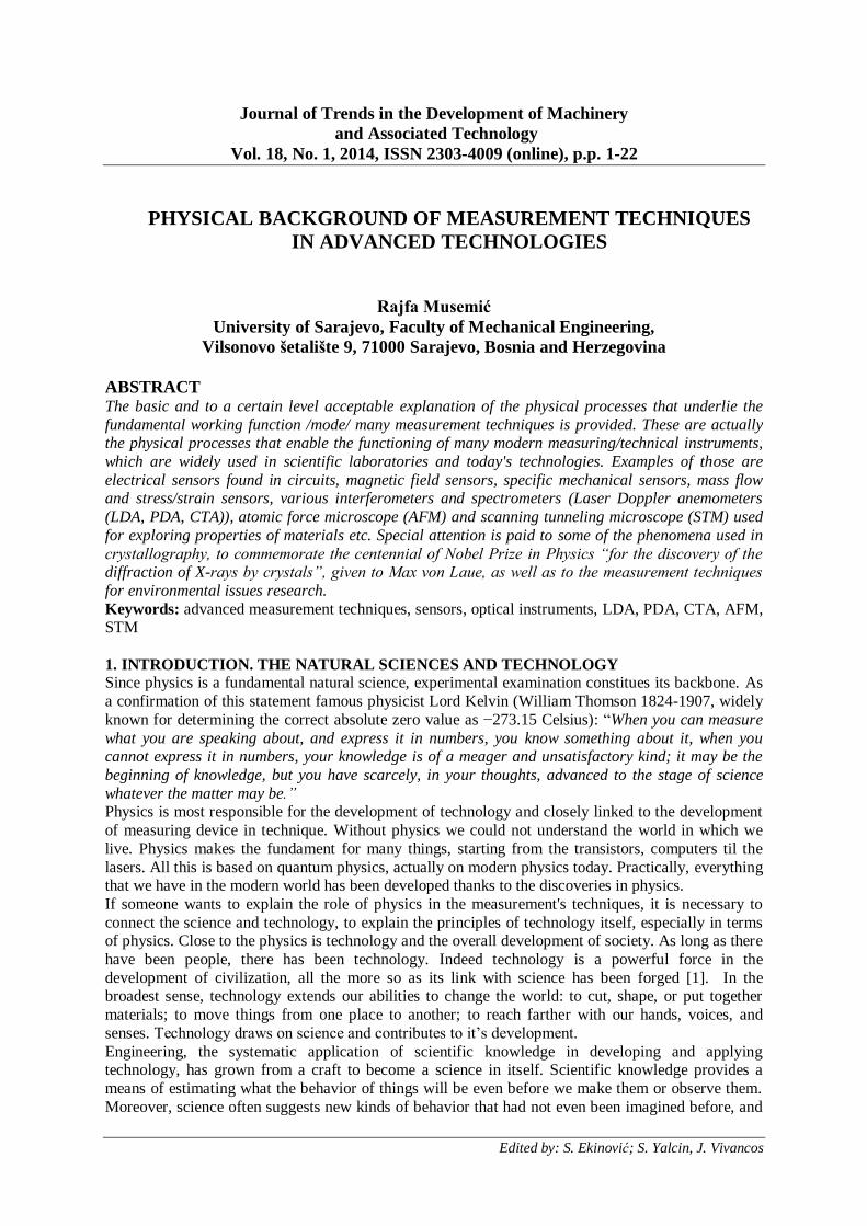
- Hall Effect – short description
If charges flow (thus establishing an electric current) through a conductor in a magnetic field, the
magnetic field exerts a transverse force on the moving charges which tends to push them to one side
of the conductor. This is most evident in a thin flat conductor as illustrated on Figure 1. A buildup of charges at the sides of the conductors will continue until it balances the magnetic influence, producing
a measurable voltage between the two sides of the conductor. The presence of this measurable
transverse voltage is called the Hall effect. The direction of the current I in the diagram is that of conventional currents, so that the motion of electrons is in the opposite direction. That further
confuses all the „right-hand-rule“ manipulations you have to go through to get the direction of the
forces.
4
The Hall voltage is given by den
BIVH , where
n is density mobile charges, and e electron
charge. The Hall effect can be used to measure magnetic fields with a Hall probe, power of
electric current, angular torque of electric engine
and electric current in conductor without contact. Furthermore, two Nobel prizes (1985, 1998)
were awarded to the Hall effect discoveries
(classical and quantum). The basic physical principle underlying the Hall effect is the
Lorentz force, which is a combination of two
separate forces: the electric force and the
magnetic force. When an electron moves along the electric field direction perpendicular to an
applied magnetic field, it experiences a magnetic force Bxvq acting normal to both
directions. Lorentz force F is therefore equal to )( BxvEq , where q is the elementary charge,
E is the electric field, v is the particle velocity, and B is the magnetic field.
2.3. Thermodynamics
Thermodynamics is a branch of physics concerned with heat and temperature and their relation to
energy and work. It defines macroscopic variables, such as internal energy, entropy, and pressure that
partly describe a body of matter or radiation. It states that the behavior of those variables is subject to general constraints, that are common to all materials, not the peculiar properties of particular
materials. These general constraints are expressed in the four laws of thermodynamics.
Thermodynamics describes the bulk behavior of the body, not the microscopic behaviors of the very
large numbers of its microscopic constituents, such as molecules. Temperature measurement is based on the following phenomena /physical principles/:
Electromagnetic spectroscopy [It is study of the interaction between matter and radiated energy. It
originated through the study of visible light dispersed according to its wavelength, e.g., by a prism. The concept was expanded to comprise any interaction with radiative energy as a function of its
wavelength or frequency. The data are often represented by a spectrum, a plot of the response of
interest as a function of wavelength]; different types of thermometers operating principles [Galileo;
gas thermometer principle: relation between temperature and volume or pressure of a gas – Gas laws; constant pressure and constant volume gas thermometer; liquid crystal thermometer; Liquid
thermometer principle: relation between temperature and volume of a liquid; Alcohol and Mercury-in-
glass thermometer; Pyrometers principle: temperature dependence of spectral intensity of light (Planck's law), i.e. the color of the light relates to the temperature of its source, measurement of
thermal radiation (instead of thermal conduction, or convection) means: Resistance thermometer
principle: relation between temperature and electrical resistance of metals, usually platinum; solid thermometer principles: relation between temperature and length of a solid (Coefficient of thermal
expansion) Bi-metallic strip; Thermistors principle: relation between temperature and electrical
resistance of ceramics or polymers, Thermocouples principle: relation between temperature and
voltage of metal junctions (Seebeck effect), Triple Point cell used for calibrating thermometers].
2.4. Oscillations, waves and optics
This area covers the processes like oscillations, propagation of waves, light waves, reflection, refraction, interference, diffraction and polarization. This also includes sound, compression waves in
matter, sound pressure, sound intensity, hearing, and loudness. The wave phenomena and optics did
left the biggest mark on the development of measurement techniques. Photonics, fiberoptics, interferometry, diffraction, thermovision and laser techniques are in the field of advanced physics and
phenomena that have experienced the greatest growth and expansion in modern technology and
measurement’ techniques at all.
Figure 1. Schetch for Hall effect (Credit: [7])
5
- Interferometry
The phenomena related to electromagnetic waves and light have complex consequences for many processes. The mathematics behind ELM descriptions, Maxwell's equations, are very belaboring and
strenuous. A lot about the way we think of light in a wave form, just as electromagnetic wave,
however, comes from Huygen's Principle of 1678. His principle states that "all points on a given
wave front are taken as point sources for the production of spherical secondary waves, called wavelets, which propagate outward with speeds characteristic of waves in that medium"[4]. This
principle becomes very important for diffraction analisys.
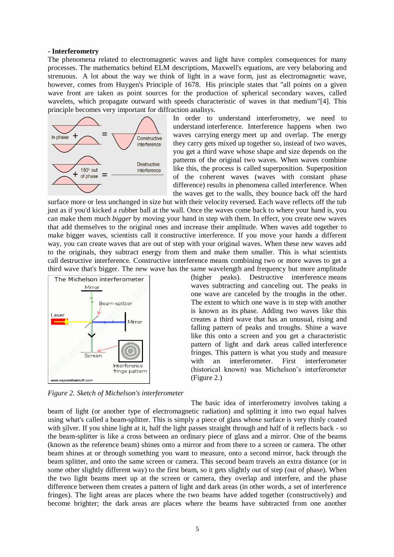
In order to understand interferometry, we need to understand interference. Interference happens when two
waves carrying energy meet up and overlap. The energy
they carry gets mixed up together so, instead of two waves, you get a third wave whose shape and size depends on the
patterns of the original two waves. When waves combine
like this, the process is called superposition. Superposition
of the coherent waves (waves with constant phase difference) results in phenomena called interference. When
the waves get to the walls, they bounce back off the hard
surface more or less unchanged in size but with their velocity reversed. Each wave reflects off the tub just as if you'd kicked a rubber ball at the wall. Once the waves come back to where your hand is, you
can make them much bigger by moving your hand in step with them. In effect, you create new waves
that add themselves to the original ones and increase their amplitude. When waves add together to make bigger waves, scientists call it constructive interference. If you move your hands a different
way, you can create waves that are out of step with your original waves. When these new waves add
to the originals, they subtract energy from them and make them smaller. This is what scientists
call destructive interference. Constructive interference means combining two or more waves to get a third wave that's bigger. The new wave has the same wavelength and frequency but more amplitude
(higher peaks). Destructive interference means
waves subtracting and canceling out. The peaks in one wave are canceled by the troughs in the other.
The extent to which one wave is in step with another
is known as its phase. Adding two waves like this
creates a third wave that has an unusual, rising and falling pattern of peaks and troughs. Shine a wave
like this onto a screen and you get a characteristic
pattern of light and dark areas called interference fringes. This pattern is what you study and measure
with an interferometer. First interferometer
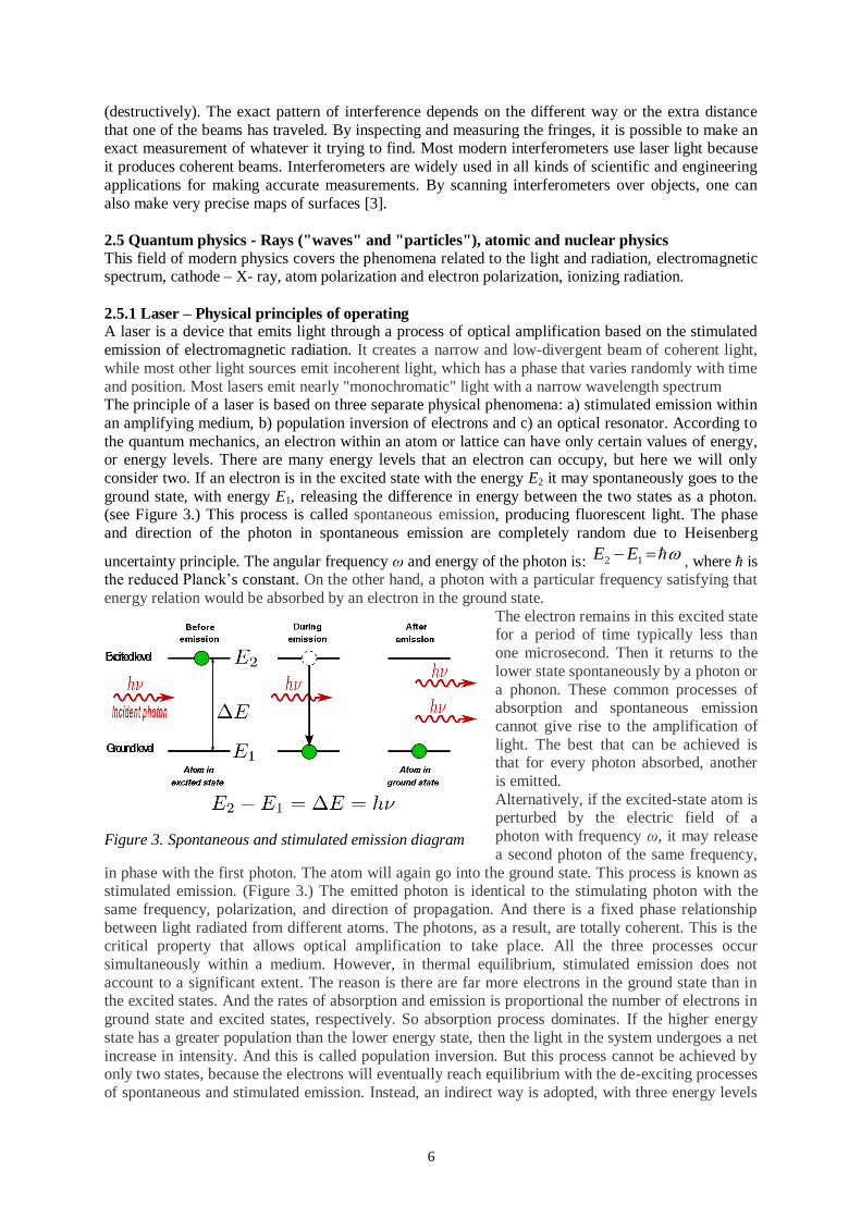
(historical known) was Michelson’s interferometer (Figure 2.)
The basic idea of interferometry involves taking a beam of light (or another type of electromagnetic radiation) and splitting it into two equal halves
using what's called a beam-splitter. This is simply a piece of glass whose surface is very thinly coated
with silver. If you shine light at it, half the light passes straight through and half of it reflects back - so the beam-splitter is like a cross between an ordinary piece of glass and a mirror. One of the beams
(known as the reference beam) shines onto a mirror and from there to a screen or camera. The other
beam shines at or through something you want to measure, onto a second mirror, back through the beam splitter, and onto the same screen or camera. This second beam travels an extra distance (or in
some other slightly different way) to the first beam, so it gets slightly out of step (out of phase). When
the two light beams meet up at the screen or camera, they overlap and interfere, and the phase
difference between them creates a pattern of light and dark areas (in other words, a set of interference fringes). The light areas are places where the two beams have added together (constructively) and
become brighter; the dark areas are places where the beams have subtracted from one another
Figure 2. Sketch of Michelson's interferometer
6
(destructively). The exact pattern of interference depends on the different way or the extra distance
that one of the beams has traveled. By inspecting and measuring the fringes, it is possible to make an exact measurement of whatever it trying to find. Most modern interferometers use laser light because
it produces coherent beams. Interferometers are widely used in all kinds of scientific and engineering
applications for making accurate measurements. By scanning interferometers over objects, one can
also make very precise maps of surfaces [3].
2.5 Quantum physics - Rays ("waves" and "particles"), atomic and nuclear physics
This field of modern physics covers the phenomena related to the light and radiation, electromagnetic spectrum, cathode – X- ray, atom polarization and electron polarization, ionizing radiation.
2.5.1 Laser – Physical principles of operating A laser is a device that emits light through a process of optical amplification based on the stimulated
emission of electromagnetic radiation. It creates a narrow and low-divergent beam of coherent light,
while most other light sources emit incoherent light, which has a phase that varies randomly with time
and position. Most lasers emit nearly "monochromatic" light with a narrow wavelength spectrum The principle of a laser is based on three separate physical phenomena: a) stimulated emission within
an amplifying medium, b) population inversion of electrons and c) an optical resonator. According to
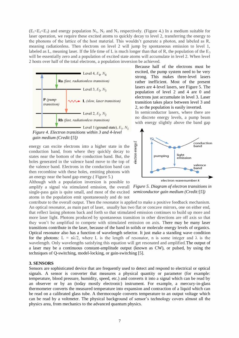
the quantum mechanics, an electron within an atom or lattice can have only certain values of energy, or energy levels. There are many energy levels that an electron can occupy, but here we will only
consider two. If an electron is in the excited state with the energy E2 it may spontaneously goes to the
ground state, with energy E1, releasing the difference in energy between the two states as a photon. (see Figure 3.) This process is called spontaneous emission, producing fluorescent light. The phase
and direction of the photon in spontaneous emission are completely random due to Heisenberg
uncertainty principle. The angular frequency ω and energy of the photon is: 12 EE , where ћ is the reduced Planck’s constant. On the other hand, a photon with a particular frequency satisfying that
energy relation would be absorbed by an electron in the ground state.
The electron remains in this excited state for a period of time typically less than
one microsecond. Then it returns to the
lower state spontaneously by a photon or
a phonon. These common processes of absorption and spontaneous emission
cannot give rise to the amplification of
light. The best that can be achieved is that for every photon absorbed, another
is emitted.
Alternatively, if the excited-state atom is perturbed by the electric field of a
photon with frequency ω, it may release
a second photon of the same frequency,
in phase with the first photon. The atom will again go into the ground state. This process is known as stimulated emission. (Figure 3.) The emitted photon is identical to the stimulating photon with the
same frequency, polarization, and direction of propagation. And there is a fixed phase relationship
between light radiated from different atoms. The photons, as a result, are totally coherent. This is the critical property that allows optical amplification to take place. All the three processes occur
simultaneously within a medium. However, in thermal equilibrium, stimulated emission does not
account to a significant extent. The reason is there are far more electrons in the ground state than in the excited states. And the rates of absorption and emission is proportional the number of electrons in
ground state and excited states, respectively. So absorption process dominates. If the higher energy
state has a greater population than the lower energy state, then the light in the system undergoes a net
increase in intensity. And this is called population inversion. But this process cannot be achieved by only two states, because the electrons will eventually reach equilibrium with the de-exciting processes
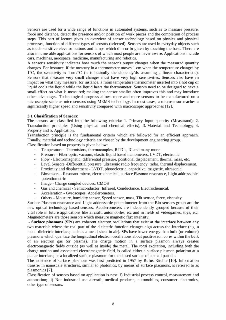
of spontaneous and stimulated emission. Instead, an indirect way is adopted, with three energy levels
Figure 3. Spontaneous and stimulated emission diagram
7
(E1<E2<E3) and energy population N1, N2 and N3 respectively. (Figure 4.) In a medium suitable for
laser operation, we require these excited atoms to quickly decay to level 2, transferring the energy to the phonons of the lattice of the host material. This wouldn’t generate a photon, and labeled as R,
meaning radiationless. Then electrons on level 2 will jump by spontaneous emission to level 1,
labeled as L, meaning laser. If the life time of L is much longer than that of R, the population of the E3
will be essentially zero and a population of excited state atoms will accumulate in level 2. When level 2 hosts over half of the total electrons, a population inversion be achieved.
Because half of the electrons must be
excited, the pump system need to be very strong. This makes three-level lasers
rather inefficient. Most of the present
lasers are 4-level lasers, see Figure 5. The population of level 2 and 4 are 0 and
electrons just accumulate in level 3. Laser
transition takes place between level 3 and
2, so the population is easily inverted. In semiconductor lasers, where there are
no discrete energy levels, a pump beam
with energy slightly above the band gap
energy can excite electrons into a higher state in the
conduction band, from where they quickly decay to states near the bottom of the conduction band. But, the
holes generated in the valence band move to the top of
the valence band. Electrons in the conduction band can
then recombine with these holes, emitting photons with an energy near the band gap energy.( Figure 5.)
Although with a population inversion is possible to
amplify a signal via stimulated emission, the overall single-pass gain is quite small, and most of the excited
atoms in the population emit spontaneously and do not
contribute to the overall output. Then the resonator is applied to make a positive feedback mechanism. An optical resonator, as main part of laser, usually has two flat or concave mirrors, one on either end,
that reflect lasing photons back and forth so that stimulated emission continues to build up more and
more laser light. Photons produced by spontaneous transition in other directions are off axis so that
they won’t be amplified to compete with stimulated emission on axis. There may be many laser transitions contribute in the laser, because of the band in solids or molecule energy levels of organics.
Optical resonator also has a function of wavelength selector. It just make a standing wave condition
for the photons: L = nλ/2, where L is the length of resonator, n is some integer and λ is the wavelength. Only wavelengths satisfying this equation will get resonated and amplified.The output of
a laser may be a continuous constant-amplitude output (known as CW), or pulsed, by using the
techniques of Q-switching, model-locking, or gain-switching [5].
3. SENSORS
Sensors are sophisticated device that are frequently used to detect and respond to electrical or optical
signals. A sensor is converter that measures a physical quantity or parameter (for example: temperature, blood pressure, humidity, speed, etc.) and converts it into a signal which can be read by
an observer or by an (today mostly electronic) instrument. For example, a mercury-in-glass
thermometer converts the measured temperature into expansion and contraction of a liquid which can be read on a calibrated glass tube. A thermocouple converts temperature to an output voltage which
can be read by a voltmeter. The physical background of sensor’s technology covers almost all the
physics area, from mechanics to the advanced quantum physics.
Figure 4. Electron transitions within 3 and 4-level
gain medium (Credit:[5])
Figure 5. Diagram of electron transitions in
semiconductor gain medium (Credit:[5])
8
Sensors are used for a wide range of functions in automated systems, such as to measure pressure,
force and distance, detect the presence and/or position of work pieces and the completion of process steps. This part of lecture gives an overview of sensor technology based on physics and physical
processes, function of different types of sensors (selected). Sensors are used in everyday objects such
as touch-sensitive elevator buttons and lamps which dim or brighten by touching the base. There are
also innumerable applications for sensors of which most people are never aware. Applications include cars, machines, aerospace, medicine, manufacturing and robotics.
A sensor's sensitivity indicates how much the sensor's output changes when the measured quantity
changes. For instance, if the mercury in a thermometer moves 1 cm when the temperature changes by 1°C, the sensitivity is 1 cm/°C (it is basically the slope dy/dx assuming a linear characteristic).
Sensors that measure very small changes must have very high sensitivities. Sensors also have an
impact on what they measure; for instance, a room temperature thermometer inserted into a hot cup of liquid cools the liquid while the liquid heats the thermometer. Sensors need to be designed to have a
small effect on what is measured; making the sensor smaller often improves this and may introduce
other advantages. Technological progress allows more and more sensors to be manufactured on a
microscopic scale as microsensors using MEMS technology. In most cases, a microsensor reaches a significantly higher speed and sensitivity compared with macroscopic approaches [12].
3.1 Classification of Sensors: The sensors are classified into the following criteria: 1. Primary Input quantity (Measurand); 2.
Transduction principles (Using physical and chemical effects); 3. Material and Technology; 4.
Property and 5. Application. Transduction principle is the fundamental criteria which are followed for an efficient approach.
Usually, material and technology criteria are chosen by the development engineering group.
Classification based on property is given below:
- Temperature - Thermistors, thermocouples, RTD’s, IC and many more.
- Pressure - Fiber optic, vacuum, elastic liquid based manometers, LVDT, electronic. - Flow - Electromagnetic, differential pressure, positional displacement, thermal mass, etc.
- Level Sensors -Differential pressure, ultrasonic radio frequency, radar, thermal displacement.
- Proximity and displacement - LVDT, photoelectric, capacitive, magnetic, ultrasonic.
- Biosensors - Resonant mirror, electrochemical, surface Plasmon resonance, Light addressable
potentiometric
- Image - Charge coupled devices, CMOS
- Gas and chemical - Semiconductor, Infrared, Conductance, Electrochemical.
- Acceleration - Gyroscopes, Accelerometers. - Others - Moisture, humidity sensor, Speed sensor, mass, Tilt sensor, force, viscosity.
Surface Plasmon resonance and Light addressable potentiometer from the Bio-sensors group are the
new optical technology based sensors. Accelerometers are independently grouped because of their
vital role in future applications like aircraft, automobiles, etc and in fields of videogames, toys, etc. Magnetometers are those sensors which measure magnetic flux intensity.
- Surface plasmons (SPs) are coherent electron oscillations that exist at the interface between any
two materials where the real part of the dielectric function changes sign across the interface (e.g. a
metal-dielectric interface, such as a metal sheet in air). SPs have lower energy than bulk (or volume) plasmons which quantize the longitudinal electron oscillations about positive ion cores within the bulk
of an electron gas (or plasma). The charge motion in a surface plasmon always creates
electromagnetic fields outside (as well as inside) the metal. The total excitation, including both the charge motion and associated electromagnetic field, is called either a surface plasmon polariton at a
planar interface, or a localized surface plasmon for the closed surface of a small particle.
The existence of surface plasmons was first predicted in 1957 by Rufus Ritchie [10]. Information
transfer in nanoscale structures, similar to photonics, by means of surface plasmons, is referred to as plasmonics [7].
Classification of sensors based on application is next: i) Industrial process control, measurement and
automation; ii) Non-industrial use–aircraft, medical products, automobiles, consumer electronics, other type of sensors.

9
Classification based on power or energy supply requirement of the sensors: i) Active sensor - Sensors
that require power supply are called as active sensors. Example: LiDAR (Light detection and ranging), photoconductive cell.
ii) Passive sensor - Sensors that do not require power supply are called as passive sensors. Example:
Radiometers, film photography.
Figure 6. Schematic representation of an electron density wave propagating along a metal –
dielectric interface. The charge density oscillations and associated electromagnetic fields are called
surface plasmon – polariton waves. The exponential dependence of the electromagnetic field intensity on the distance away from the interface is shown on the right. These waves can be excited very
efficiently with light in the visible range of the electromagnetic spectrum. (Credit: [9])
There are several group of sensors, like 1) Accelerometers /based on the micro electro mechanical
sensor technology and used for patient monitoring which includes pace makers and vehicle dynamic
systems; 2) Biosensors /based on the electrochemical technology, used for food testing, medical care
device, water testing, and biological warfare agent detection; 3) Image Sensors /based on the CMOS technology, used in electronics, biometrics, traffic and security surveillance and PC imaging.
3.2 Sensor Technology based on physics and physical phenomena - Piezoelectric effect basics: A piezoelectric substance is one that produces an electric charge when a
mechanical stress is applied (the substance is squeezed or stretched). Conversely, a mechanical
deformation (the substance shrinks or expands) is produced when an electric field is applied. This
effect is formed in crystals that have no center of symmetry. To explain this, look at the individual molecules that make up the crystal. Each molecule has a polarization. They form a dipole. This is a
result of the atoms that make up the molecule and the way the molecules are shaped. In a monocrystal
the polar axes of all of the dipoles lie in one direction, so the crystal is said to be symmetrical. In a polycrystal, there are different regions within the material that have a different polar axis. It is
asymmetrical. In order to produce the piezoelectric effect, the polycrystal is heated under the
application of a strong electric field. The heat allows the molecules to move more freely and the electric field forces all of the dipoles in the crystal to line up and face in nearly the same direction
(Figure 7). The piezoelectric effect can now be observed in the crystal. If the material is compressed,
then a voltage of the same polarity as the poling voltage will appear between the electrodes. If
stretched, a voltage of opposite polarity will appear. Conversely, if a voltage is applied the material will deform. A voltage with the opposite polarity as the poling voltage will cause the material to
expand, and a voltage with the same polarity will cause the material to compress. If an AC signal is
applied then the material will vibrate at the same frequency as the signal.
Figure 7. Polarization of Ceramic Material to Generate Piezoelectric Effect (Credit: [11])
10
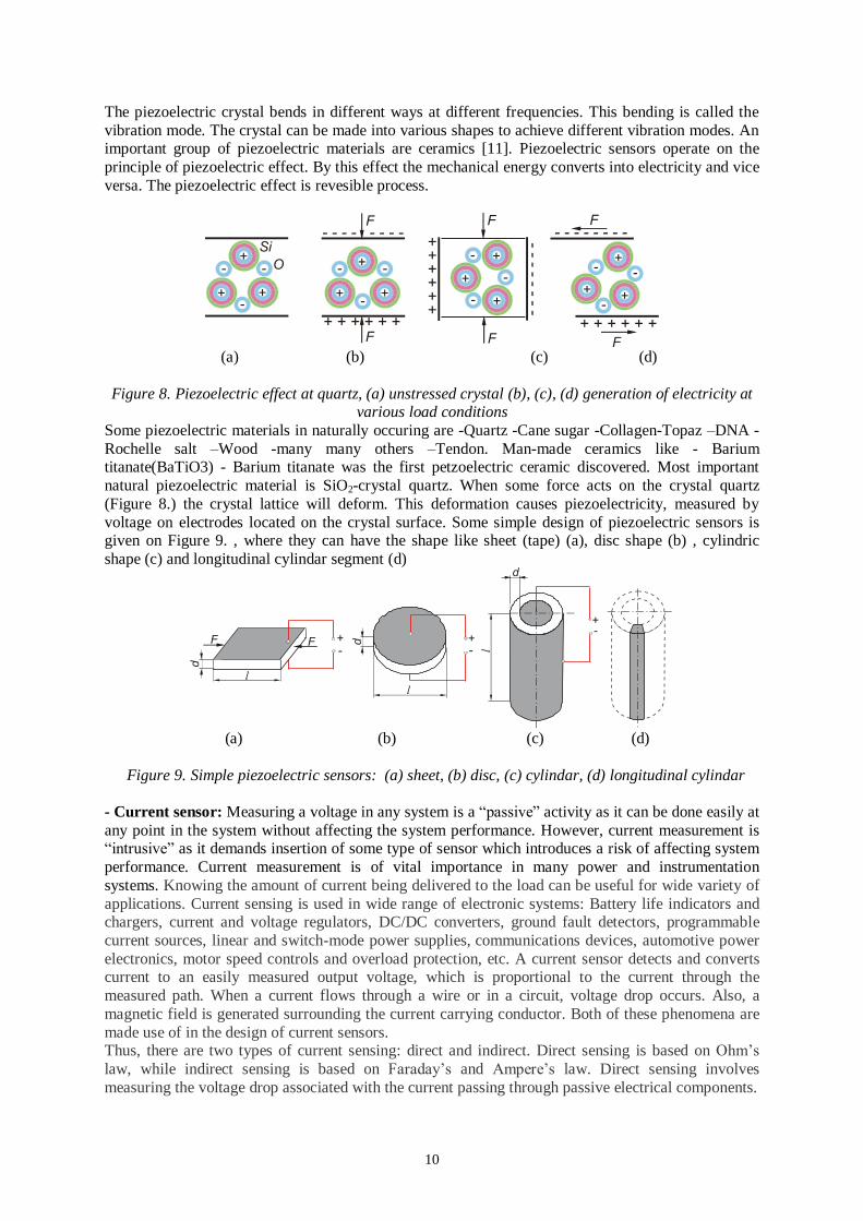
The piezoelectric crystal bends in different ways at different frequencies. This bending is called the
vibration mode. The crystal can be made into various shapes to achieve different vibration modes. An important group of piezoelectric materials are ceramics [11]. Piezoelectric sensors operate on the
principle of piezoelectric effect. By this effect the mechanical energy converts into electricity and vice
versa. The piezoelectric effect is revesible process.
(a) (b) (c) (d)
Figure 8. Piezoelectric effect at quartz, (a) unstressed crystal (b), (c), (d) generation of electricity at various load conditions
Some piezoelectric materials in naturally occuring are -Quartz -Cane sugar -Collagen-Topaz –DNA -
Rochelle salt –Wood -many many others –Tendon. Man-made ceramics like - Barium titanate(BaTiO3) - Barium titanate was the first petzoelectric ceramic discovered. Most important
natural piezoelectric material is SiO2-crystal quartz. When some force acts on the crystal quartz
(Figure 8.) the crystal lattice will deform. This deformation causes piezoelectricity, measured by
voltage on electrodes located on the crystal surface. Some simple design of piezoelectric sensors is given on Figure 9. , where they can have the shape like sheet (tape) (a), disc shape (b) , cylindric
shape (c) and longitudinal cylindar segment (d)
(a) (b) (c) (d)
Figure 9. Simple piezoelectric sensors: (a) sheet, (b) disc, (c) cylindar, (d) longitudinal cylindar
- Current sensor: Measuring a voltage in any system is a “passive” activity as it can be done easily at
any point in the system without affecting the system performance. However, current measurement is “intrusive” as it demands insertion of some type of sensor which introduces a risk of affecting system
performance. Current measurement is of vital importance in many power and instrumentation
systems. Knowing the amount of current being delivered to the load can be useful for wide variety of
applications. Current sensing is used in wide range of electronic systems: Battery life indicators and chargers, current and voltage regulators, DC/DC converters, ground fault detectors, programmable
current sources, linear and switch-mode power supplies, communications devices, automotive power
electronics, motor speed controls and overload protection, etc. A current sensor detects and converts current to an easily measured output voltage, which is proportional to the current through the
measured path. When a current flows through a wire or in a circuit, voltage drop occurs. Also, a
magnetic field is generated surrounding the current carrying conductor. Both of these phenomena are
made use of in the design of current sensors. Thus, there are two types of current sensing: direct and indirect. Direct sensing is based on Ohm’s
law, while indirect sensing is based on Faraday’s and Ampere’s law. Direct sensing involves
measuring the voltage drop associated with the current passing through passive electrical components.

11
Indirect sensing involves measurement of the magnetic field surrounding a conductor through which
current passes. Generated magnetic field is then used to induce proportional voltage or current which is then transformed to a form suitable for measurement and/or control system. The traditional way of
current sensing introduces a resistor in the path of the current to be sensed. The sense resistor can be
placed in series with the inductor, switches, and the load. Thus, a current sensing resistor should be
considered as a current-to-voltage converter. - Sensors and transducers: Simple stand alone electronic circuits can be made to repeatedly flash a
light or play a musical note, but in order for an electronic circuit or system to perform any useful task
or function it needs to be able to communicate with the “real world” whether this is by reading an input signal from an “ON/OFF” switch or by activating some form of output device to illuminate a
single light. An electronic system or circuit must be able to “do” something and sensors and
transducers are the perfect components for doing this. The word “Transducer” is the collective term used for both sensors which can be used to sense a wide range of different energy forms such as
movement, electrical signals, radiant energy, thermal or magnetic energy etc, and actuators which can
be used to switch voltages or currents. There are many different types of sensors and transducers, both
analogue and digital and input and output available to choose from. The type of input or output transducer being used, really depends upon the type of signal or process being “Sensed” or
“Controlled” but we can define a sensor and transducers as devices that converts one physical quantity
into another. Devices which perform an “Input” function are commonly called sensors. Devices which perform an “Output” function are generally called actuators and are used to control some external
device, for example movement or sound. Electrical transducers are used to convert energy of one kind
into energy of another kind. For example a microphone (input device) converts sound waves into electrical signals for the amplifier to amplify (a process), and a loudspeaker (output device) converts
these electrical signals back into sound waves (Figure 10.).
Figure 10. Simple Input/Output system using sound transducers, (Credit: [14])
Analog sensors produce a continuous output signal or voltage which is generally proportional to the
quantity being measured. Physical quantities such as temperature, speed, pressure, displacement,
strain etc. are all analogue quantities as they tend to be continuous in nature. Analogue sensors tend to produce output signals that are changing smoothly and continuously over time. Then circuits which
measure analogue signals usually have a slow response and/or low accuracy. Also analogue signals
can be converted into digital type signals for use in micro-controller systems by the use of analogue-to-digital converters (Figure 11.) [14].
Figure 11. Left) Thermocouple used to produce an analogue signal, Right) a digital signal
12
- Electromagnetic sensors: Principle of electromagnetic sensor operating is based on the dependence
of the change in inductance of solenoid electromagnetic circuits or electromagnetic induction. Because of that they can be classifird into inductive which are passive sensors, and induction's which
are active sensors. Both of them are operating on non-contacting principle and the sensor's mass does
not influence on the measurements results.
- Inductive sensors: Inductance of the solenoid with a ferromagnetic corel and the air gap is
calculated as 2
02
hN AL
h where μ0 is magnetic permeability of vacuum, N number of coils, h width
of gap and Ah crosssection of gap area. The magnetic quantities μ0, N and magnetic circuit geometry
are changing upon the influence of mechanical quantities, and this principle of parameters variation is
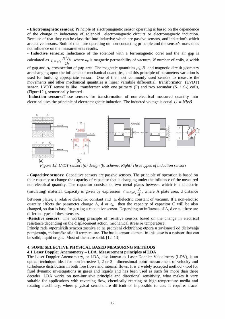
used for building appropriate sensor. One of the most commonly used sensors to measure the movements and other mechanical quantities is linear variabile differential transformator (LVDT)
sensor. LVDT sensor is like transformer with one primary (P) and two secundar (S1 i S2) coils,
(Figure12.), symetrically located. -Induction sensors:These sensors for transformation of non-electrical measured quantity into
electrical uses the principle of electromagnetic induction. The inducted voltage is equal NlvBU .
(a) (b)
Figure 12. LVDT sensor, (a) design (b) scheme; Right) Three types of induction sensors
- Capacitive sensors: Capacitive sensors are passive sensors. The principle of operation is based on
their capacity to change the capacity of capacitor that is changing under the influence of the measured
non-electrical quantity. The capacitor consists of two metal plates between which is a dielectric
(insulating) material. Capacity is given by expression 0 r
AC
d , where A plate area, d distance
between plates, εr relative dielectric constant and ε0 dielectric constant of vacuum. If a non-electric quantity affects the parameter change A, d or εr, then the capacity of capacitor C will be also
changed, so that is base for getting a capacitive sensor. Depending on influence of A, d or εr, there are
different types of these sensors. -Resistive sensors: The working principle of resistive sensors based on the change in electrical
resistance depending on the displacement action, mechanical stress or temperature .
Princip rada otporničkih senzora zasniva se na promjeni električnog otpora u zavisnosti od djelovanja pomjeranja, mehaničke sile ili temperature. The basic sensor element in this case is a resistor that can
be solid, liquid or gas. Most of them are solid. [12, 13]
4. SOME SELECTIVE PHYSICAL BASED MEASURING METHODS
4.1 Laser Doppler Anemometry – LDA. Measurement principles of LDA
The Laser Doppler Anemometry, or LDA, also known as Laser Doppler Velocimetry (LDV), is an
optical technique ideal for non-intrusive 1, 2 or 3 - dimensional point measurement of velocity and turbulence distribution in both free flows and internal flows. It is a widely accepted method - tool for
fluid dynamic investigations in gases and liquids and has been used as such for more than three
decades. LDA works on non-intrusive principle and directional sensitivity, what makes it very
suitable for applications with reversing flow, chemically reacting or high-temperature media and rotating machinery, where physical sensors are difficult or impossible to use. It requires tracer

13
particles in the flow. The method's
particular advantages are: non-intrusive measurement, high spatial
and temporal resolution, no need for
calibration and the ability to
measure in reversing flows. Measurement flow velocity of fluid
by laser anemometry is based on
detection of Doppler shift frequency of scattered light on tracers flow
during motion over the measurable
area. The Doppler effect is observed
whenever the source of waves is
moving with respect to an observer.
The Doppler effect produced by a moving source of waves in which
there is an apparent upward shift in
frequency for observers towards whom the source is approaching and
an apparent downward shift in frequency for observers from whom the source is receding. It is
important to note that the effect does not result because of an actual change in the frequency of the source. The effect is only observed because the distance between observer (receiver) and the emitter
(source) is decreasing and the distance between observer and source is increasing. The Doppler effect
can be observed for any type of wave - water wave, sound wave, light wave, etc. We are most familiar
with the Doppler effect because of our experiences with sound waves. Perhaps you recall an instance in which a police car or emergency vehicle was traveling towards you on the highway. As the car
approached with its siren blasting, the pitch of the siren sound (a measure of the siren's frequency)
was high; and then suddenly after the car passed by, the pitch of the siren sound was low. That was the Doppler effect - an apparent shift in frequency for a sound wave produced by a moving source.
Doppler shift was given by Christian Johann Doppler in 1842. This apparent change in the frequency
of sound as a result of relative motion between the source and the observer is the Doppler effect.
There are eight Doppler effect formulas for frequency depending on cases: (i) When the source is moving towards or away (sign + in denominator) a observer at rest
fvv
vf
s'
(ii) When observer is moving towards or away
from the stationary source
fv
vvf o )('
. (iii) When both source and
observer moves towards each other
fvv
vvf
s
o
)(
)('
, or the source is approaching
the stationary observer and iv) observer
moving away from source and when the observer is approaching the stationary source
fvv
vvf
s
o
)(
)('
, where vs = velocity of the source, vo = velocity of the observer, v = velocity of sound
or light in medium, f = real frequency, f’ = apparent frequency.
The basic configuration of an LDA consists of: i) A continuous wave laser, ii) Transmitting optics, including a beam splitter and a focusing lens, iii) Receiving optics, comprising a focusing lens, an
interference filtre and photodetector and iv) A signal conditioner and a signal processor. Advanced
systems may include traverse systems and angular encoders. A Bragg cell is often used as the beam
Figure 13. LDA system configuration (Credit: [6] )
14
splitter. It is a glass crystal with a vibrating piezo-crystal attached. The vibration generates acoustical
waves acting like an optical grid. The output of the Bragg cell is two beams of equal intensity with frequencies f0 and fshift. These are focused into optical fibres bringing them to a probe. In the probe, the
parallel exit beams from the fibres are focused by a lens to intersect in the probe volume [6]. The light
intensity is modulated due to interference between the laser beams. This produces parallel planes of
high light intensity, so called fringes. The fringe distance df is defined by the wavelength of the laser
light and the angle between the beams: )2/sin(2
fd
.
Each particle passage scatters light
proportional to the local light intensity. Flow velocity information comes from light scattered by tiny "seeding" particles carried in the fluid as they move through the probe volume. The scattered light
contains a Doppler shift, the Doppler frequency fD, which is proportional to the velocity component
perpendicular to the bisector of the two laser beams, which corresponds to the x axis shown in the probe volume. The scattered light is collected by a receiver lens and focused on a photo-detector. The
photo-detector converts the fluctuating light intensity to an electrical signal, the Doppler burst, which
is sinusoidal with a Gaussian envelope due to the intensity profile of the laser beams. The Doppler
bursts are filtered and amplified in the signal processor, which determines fD for each particle, using the robust Fast Fourier Transform (FFT) algorithm. The fringe spacing, df provides information about
the distance travelled by the particle. The Doppler frequency fD provides information about the time: t
= 1/ fD , while velocity is v = df . fD . The frequency shift obtained by the Bragg cell makes the fringe
pattern move at a constant velocity. Particles which are not moving will generate a signal of the shift
frequency fshift. The velocities Upos and Uneg will generate signal frequencies fpos and fneg,
respectively. LDA systems without frequency shift cannot distinguish positive and negative flow direction, but LDA systems with frequency shift can do it. [6]
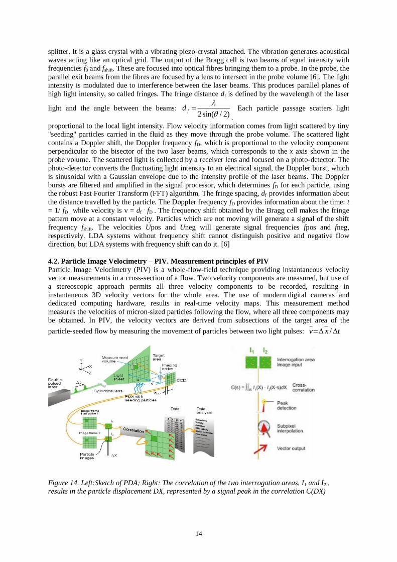
4.2. Particle Image Velocimetry – PIV. Measurement principles of PIV
Particle Image Velocimetry (PIV) is a whole-flow-field technique providing instantaneous velocity vector measurements in a cross-section of a flow. Two velocity components are measured, but use of
a stereoscopic approach permits all three velocity components to be recorded, resulting in
instantaneous 3D velocity vectors for the whole area. The use of modern digital cameras and dedicated computing hardware, results in real-time velocity maps. This measurement method
measures the velocities of micron-sized particles following the flow, where all three components may
be obtained. In PIV, the velocity vectors are derived from subsections of the target area of the
particle-seeded flow by measuring the movement of particles between two light pulses: txv /
Figure 14. Left:Sketch of PDA; Right: The correlation of the two interrogation areas, I1 and I2 , results in the particle displacement DX, represented by a signal peak in the correlation C(DX)
(Credit: [6] )

15
The flow is illuminated in the target area with a light sheet. The
camera lens images the target area onto the sensor array of a digital camera. The camera is able to capture each light pulse
in separate image frames. Once a sequence of two light pulses
is recorded, the images are divided into small subsections
called interrogation areas (IA). The interrogation areas from each image frame, I1 and I2, are cross-correlated with each
other, pixel by pixel. The correlation produces a signal peak,
identifying the common particle displacement, DX. A velocity vector map over the whole target area is obtained by repeating
the cross-correlation for each interrogation area over the two
image frames captured by the camera. (Figure 14.) PIV images are visual, just follow the seeding. Recording both light pulses
in the same image frame to track the movements of the
particles gives a clear visual sense of the flow structure. The number of particles in the flow is of
some importance in obtaining a good signal peak in the cross-correlation. When the size of the interrogation area, the magnification of the imaging and the light-sheet thickness are known, the
measurement volume can be defined. In normal PIV systems, the third velocity component is
''invisible'' due to the geometry of the imaging. This third velocity component can be derived by using two cameras in a stereoscopic arrangement.
4.3. Particle Doppler Anemometry – PDA. Measurement principles of PDA PDA measurements are performed on single particles, allowing for detailed analysis of particulate
flows. The distribution of statistical size and velocity moments in a flow field can be measured, as
well as particle concentration and local size-velocity correlation. Movement of the measurement point
in the flow allows mapping of entire flow fields. The underlying principle of phase Doppler anemometry is based on light-scattering interferometry and therefore requires no calibration.
The measurement point is defined by the intersection of two focused laser beams and the
measurements are performed on single particles as they move through the sample volume. Particles thereby scatter light from both laser beams, generating an optical interference pattern. A receiving
optics placed at a well-chosen off-axis location projects a portion of the scattered light onto multiple
detectors. Each detector converts the optical signal into a Doppler burst. The phase shift between the
Doppler signals from different detectors is a direct measure of the particle diameter. The PDA technique is an extension of LDA and is based upon phase Doppler principles. Two or more detectors
collect the light scattered by single particles passing through the measurement volume.
The phenomena of light scattering can be visualised by ray tracing. The light which is incident on e.g. a water droplet is partially reflected from the surface and partially transmitted and refracted in both
forward and backward directions after one internal reflection. The scattered light intensity depends on
the relative refractive index. Particle velocity U is calculated from the Doppler frequency fD of the
signal from any one of the detectors: DfU
)2/sin(2
. The particle size D is derived from the phase
difference between the signals from two detectors. If light scattering is dominated by reflection:
)coscoscos1(2
sinsin2
D
.
If it is dominated by refraction:
))coscoscos1(21)(coscoscos1(2
sinsin2
2
relrel
rel
nn
nD
.
The maximum particle size that can be unambiguously measured with two detectors corresponds to a
phase shift of Ф1-2 = 360°. Reducing the distance between the detectors can extend the particle size
range. This however, will also reduce the measurement resolution. Using three detectors provides both a large measurable size range (Ф1-3 ) and a high measurement resolution (Ф1-2 ). [6, 8]
Figure 15. Double-pulsed particle
images (Credit: [6] )
16
4.4. Constant Temperature Anemometry (CTA) – Hot-Wire Anemometry – Thermal
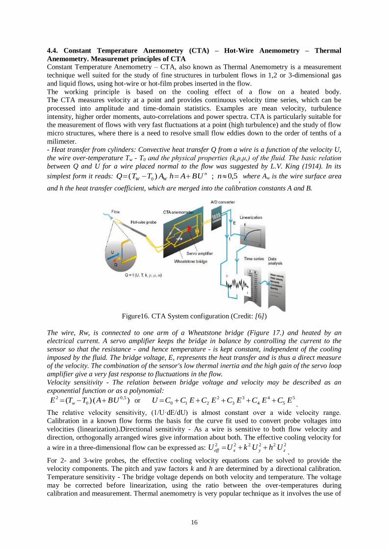
Anemometry. Measuremet principles of CTA Constant Temperature Anemometry – CTA, also known as Thermal Anemometry is a measurement
technique well suited for the study of fine structures in turbulent flows in 1,2 or 3-dimensional gas
and liquid flows, using hot-wire or hot-film probes inserted in the flow.
The working principle is based on the cooling effect of a flow on a heated body. The CTA measures velocity at a point and provides continuous velocity time series, which can be
processed into amplitude and time-domain statistics. Examples are mean velocity, turbulence
intensity, higher order moments, auto-correlations and power spectra. CTA is particularly suitable for the measurement of flows with very fast fluctuations at a point (high turbulence) and the study of flow
micro structures, where there is a need to resolve small flow eddies down to the order of tenths of a
milimeter. - Heat transfer from cylinders: Convective heat transfer Q from a wire is a function of the velocity U,
the wire over-temperature Tw - T0 and the physical properties (k,ρ,μ,) of the fluid. The basic relation
between Q and U for a wire placed normal to the flow was suggested by L.V. King (1914). In its
simplest form it reads: 5,0;)( 0 nUBAhATTQ n
WW , where Aw is the wire surface area
and h the heat transfer coefficient, which are merged into the calibration constants A and B.
Figure16. CTA System configuration (Credit: [6])
The wire, Rw, is connected to one arm of a Wheatstone bridge (Figure 17.) and heated by an electrical current. A servo amplifier keeps the bridge in balance by controlling the current to the
sensor so that the resistance - and hence temperature - is kept constant, independent of the cooling
imposed by the fluid. The bridge voltage, E, represents the heat transfer and is thus a direct measure of the velocity. The combination of the sensor's low thermal inertia and the high gain of the servo loop
amplifier give a very fast response to fluctuations in the flow.
Velocity sensitivity - The relation between bridge voltage and velocity may be described as an
exponential function or as a polynomial:
)()( 5,0
0
2 UBATTE w or 5
5
4
4
3
3
2
210 ECECECECECCU .
The relative velocity sensitivity, (1/U·dE/dU) is almost constant over a wide velocity range. Calibration in a known flow forms the basis for the curve fit used to convert probe voltages into
velocities (linearization).Directional sensitivity - As a wire is sensitive to both flow velocity and
direction, orthogonally arranged wires give information about both. The effective cooling velocity for
a wire in a three-dimensional flow can be expressed as: 222222
zyxeff UhUkUU .
For 2- and 3-wire probes, the effective cooling velocity equations can be solved to provide the velocity components. The pitch and yaw factors k and h are determined by a directional calibration.
Temperature sensitivity - The bridge voltage depends on both velocity and temperature. The voltage
may be corrected before linearization, using the ratio between the over-temperatures during calibration and measurement. Thermal anemometry is very popular technique as it involves the use of

17
very small probes that offer very high spatial resolution and excellent frequency response
characteristics.
Figure 17. CTA principles scheme and probes
5. NANOTECHNOLOGY
5.1 Atomic force microscopy Atomic force microscopy (AFM) is part of the family of techniques known as scanning probe microscopy, an
extremely valuable and versatile investigative tool. An
everyday example of scanning probe technique is reading the Braille alphabet–blind person moves fingers (sensitive
probes) in a scanning fashion over the surface of paper
(sample), looking for changes in friction or elevation of
paper to detect a symbol. [17, 20] Similar principle is used in AFM: a probe consisting of a
cantilever (a long beam) and a sharp tip is brought very
close to the surface of the sample. There are number of interactions between the sharp tip and sample when they
are close, but the strongest ones are the Coulomb’s strong,
short range repulsive force (from electron clouds of tip and
sample), and van der Waals interactions-longer range attractive force, (from redistribution of nearby electron
clouds) which induces temporary electric dipoles attracting
each other.
Figure 18: AFM image of the surface of
a thin film of GaN. Distance between
“terraces” and “steps” in the image is
0.25nm, corresponding to a single layer of GaN atoms. Credit: University of
Cambridge
Figure 19. AFM tip under 1000x magnification
Figure 20. Force distance graph for tip–sample
interaction
18
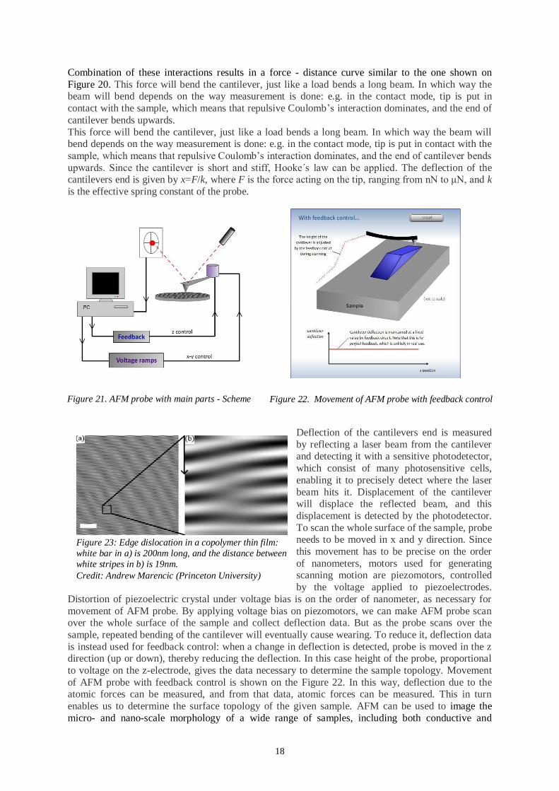
Combination of these interactions results in a force - distance curve similar to the one shown on
Figure 20. This force will bend the cantilever, just like a load bends a long beam. In which way the beam will bend depends on the way measurement is done: e.g. in the contact mode, tip is put in
contact with the sample, which means that repulsive Coulomb’s interaction dominates, and the end of
cantilever bends upwards.
This force will bend the cantilever, just like a load bends a long beam. In which way the beam will bend depends on the way measurement is done: e.g. in the contact mode, tip is put in contact with the
sample, which means that repulsive Coulomb’s interaction dominates, and the end of cantilever bends
upwards. Since the cantilever is short and stiff, Hooke´s law can be applied. The deflection of the cantilevers end is given by x=F/k, where F is the force acting on the tip, ranging from nN to μN, and k
is the effective spring constant of the probe.
Deflection of the cantilevers end is measured
by reflecting a laser beam from the cantilever and detecting it with a sensitive photodetector,
which consist of many photosensitive cells,
enabling it to precisely detect where the laser
beam hits it. Displacement of the cantilever will displace the reflected beam, and this
displacement is detected by the photodetector.
To scan the whole surface of the sample, probe needs to be moved in x and y direction. Since
this movement has to be precise on the order
of nanometers, motors used for generating scanning motion are piezomotors, controlled
by the voltage applied to piezoelectrodes.
Distortion of piezoelectric crystal under voltage bias is on the order of nanometer, as necessary for
movement of AFM probe. By applying voltage bias on piezomotors, we can make AFM probe scan over the whole surface of the sample and collect deflection data. But as the probe scans over the
sample, repeated bending of the cantilever will eventually cause wearing. To reduce it, deflection data
is instead used for feedback control: when a change in deflection is detected, probe is moved in the z direction (up or down), thereby reducing the deflection. In this case height of the probe, proportional
to voltage on the z-electrode, gives the data necessary to determine the sample topology. Movement
of AFM probe with feedback control is shown on the Figure 22. In this way, deflection due to the atomic forces can be measured, and from that data, atomic forces can be measured. This in turn
enables us to determine the surface topology of the given sample. AFM can be used to image the
micro- and nano-scale morphology of a wide range of samples, including both conductive and
Figure 23: Edge dislocation in a copolymer thin film:
white bar in a) is 200nm long, and the distance between
white stripes in b) is 19nm.
Credit: Andrew Marencic (Princeton University)
Figure 22. Movement of AFM probe with feedback control Figure 21. AFM probe with main parts - Scheme
19
insulating materials, and both soft and hard materials. For example, it can be used to image
dislocations in metals and polymers, like collagen fibril (hair), and it can be even used to take pictures of live cells in a fluid environment. As with any instrument, there are a number of problems and
artefacts that can arise during atomic force microscopy. Atomic force microscopy may be used to
image the micro- and nano-scale morphology of a wide range of samples, including both conductive
and insulating materials, and both soft and hard materials. Due to its high resolution and versatility, over the years AFM has had a significant impact in many disciplines, from materials science to
biological and medical research. It also can be used for imaging dislocations in materials and for
precise measurement of roughness. Besides that, because of its ability to image samples on an atomic scale, AFM had been and will continue to be vital to the advance of nanotechnology [16, 17].
5.2 Scannig Tunneling Microscopy – STM Scanning tunneling microscopy also belongs to the family of
scanning probe microscopy, and it shares many design
features of AFM. Scanning tunneling microscope is actually
a predecessor to AFM – it was invented in 1981. The functioning of STM is based on a purely quantum
mechanical effect called tunneling. A particle of total energy
E moves in +x direction, and on its way an energy barrier is placed /hill of height Uo between x=0 and x=L/. A simple
model of barrier would consist of 2 identical metals with a
thin insulator between them – an electron can easily move inside the metal, but cannot easily go through the insulator.
Classically, if E > Uo, the particle will always successfully go over the hill, slowing down while
going over the hill: and if E < Uo, our
particle will never be able to go over the hill, that is, it will be always reflected
back. This is certainly true for macroscopic “particles” like a ball that
is being thrown over the net. But for
small particles like electrons, quantum-mechanical effects start to play a
significant role. In quantum mechanics,
matter has characteristics of both wave (frequency, wavelength) and of a
particle (position, impulse)- this
seemingly contradictory idea, put forth by de Broglie. Another weird idea that proved to be correct was Heisenberg´s uncertainty principle. Since matter
is described as both wave and particle, a balance is
struck: if impulse/energy of matter is well known, then position/time interval is not, and vice versa.
Wave-particle duality and Heisenberg´s uncertainty
principle give rise to the phenomena of quantum tunneling. In contrary to the classical prediction,
there is a finite probability that a particle with E < Uo
will go over the energy hill and emerge on the other side of the hill. A simple way to represent the
probability of tunneling is to sketch the wave
function. In quantum mechanics, matter is mathematically described by a wave function - wave
function alone has no clear physical meaning, but its
square gives the probability density of finding the particle inside some interval. On the Figure 25. a non-zero wave function behind the barrier means
that there is a non-zero probability of finding a particle behind the barrier.
Tunneling probability T strongly depends on the length of hill L, and height difference E – Uo. This
Figure 26. Schematic overview of STM
Figure 25. Sketch of wave function of tunneling particle
Figure 24. Energy barrier
20
strong dependence on length of barrier enables STM to obtain high resolution images, comparable to
the size of a single atom. Scanning tunneling microscopes achieves such high resolution by using the basic apparatus shown in Figure 26. An electrically conductive probe with a very sharp tip is brought
near the surface of the sample, which also has to be conductive. Since both the tip and the sample are
conductive, they are the two sides of the barrier, and the empty space between them represents the barrier we have been discussing. Because electrons obey quantum rules rather than Newtonian rules,
they can “tunnel” across the barrier of empty space, thereby producing a tunneling current. If there is
no voltage between tip and sample, current is equal in both directions, resulting in zero net current - but if a voltage is applied between sample and tip, electrons in the atoms on the surface of the sample
can tunnel preferentially from surface to tip to produce a tunneling current. In this way, the tip
samples the distribution of electrons immediately above the surface. By monitoring the tunneling current as the tip is scanned over the sample, topography of the electron distribution on the surface
can be obtained (a piece of graphite is very often used as a sample, like on Figure 26.). Since
tunneling current depends strongly on the distance between surface and tip, STM has a very high resolution: 0.1 nm in lateral directions and 0.01nm depth resolution [20].
The STM has one serious limitation: Its operation depends on the electrical conductivity of the sample
and the tip. Unfortunately, most materials are not electrically conductive at their surfaces. Even metals, which are usually excellent electrical conductors, are covered with nonconductive oxides.
5.3 X – ray crystallography The X – ray crystallography is a 100 year old method which is still the most widely used method for
determining atomic structure of crystalline materials, and which has helped determine the structure of
many biological molecules like DNA, vitamins and proteins.
This method relies on using X–rays - electromagnetic radiation with wavelengths between roughly 0.01nm and 10nm, similar to the interatomic distances in a crystal. Since (visible) light diffracts when
it encounters a structure of dimension similar to its wavelengths, German physicist Max von Laue
expected to observe similar effect when a crystal is bombarded with X-rays. What he observed was diffraction, and this discovery earned him a Nobel Prize in Physics exactly 100 years ago. To
commemorate this occasion and to emphasize the global importance of crystallography in human life,
United Nations have declared year 2014 as the International Year of Crystallography. A simple model of diffraction on a surface of a
crystalline material is shown on Figure 27. X-rays
incident on two crystallographic planes are
scattered by electrons of the atoms in the material – these rays are allowed to interfere in X-ray
detector and, depending on the angles, we will
have constructive or destructive interference. By changing the incidence angle θ and measuring the
intensity of scattered beam, the data necessary to
determine characteristics of sample is obtained.
In a more realistic model, there are more
crystallographic planes, and diffraction occurs on
each one of them. Also, orientation of crystallographic planes is not necessarily parallel to the surface of the sample, and there might be more than one crystal in selected sample. Determining
characteristics of given crystals is possible in this situation, but it is necessary to use more advanced
physical models and mathematical tools to do so. X – ray crystallography has played a crucial role in characterizing many of the materials used today, and most notably, it helped determine the shape of
DNA molecule, which enabled further development of genetics. [20]
5.4. Physical aspects of smartphone camera Remote sensing is the collection of information relating to objects without being in physical contact
with them. Thus our eyes and ears are remote sensors, and the same is true for cameras and
microphones and for many instruments used in various applications. Remote sensing is the process of acquiring data/information about objects/substances not in direct contact with the sensor, by gathering
Figure 27. Simple model of diffraction on crystal

21
its inputs using electromagnetic radiation or acoustical waves that emanate from the targets of interest.
Remote sensing actually done from satellites as Landsat or airplane or on the ground. To repeat the essence of the definition above, remote sensing uses instruments that house sensors to view the
spectral, spatial and radiometric relations of observable objects and materials at a distance. Most
sensing modes are based on sampling of appropriate frequency photons in the electromagnetic (EM)
spectrum. In much of remote sensing, the process involves an interaction between incident radiation and the targets of interest. Remote sensing also involves the sensing of emitted energy and the use of
non-emitted sensors. LIDAR or LADAR (Light Detection And Ranging) is an optical remote sensing
technology that can measure the distance to, or other properties of a target by illuminating the target with light, often using pulses from a laser. LIDAR technology has application in archaeology,
geography, geology, geomorphology, seismology, forestry, remote sensing and atmospheric physics.
An aerial photograph is a common example of a remotely sensed (by camera and film, or now digital) product [19] .
We are witnesses of a tremendous growth of camera applications on smartphones these days. Every
new generation of the camera modules offers higher resolution, better pictures in a smaller (or equal
in size) package! We will discuss here some physical constrains of phone cameras. Camera of a smartphone is packed in a single module, which contains several lenses, voice coil motor which
moves some of them to focus, sensor, and connectors. Entire package is ~5mm thick, and aperture of
the front lens is about 1mm. Here is an example, LG module with 5 lenses. The size of the module can’t be increased because of the strict
requirement of design - thin profile of a smartphone. At the same
time, they offer more megapixels, which mean that individual pixels on a sensor are becoming smaller. Nowadays, size of the
pixels is so small (of order 1 mm) that it seems impossible to
make them smaller and keep the same quality of the picture.
Another problem is the diffraction. If you have a lens with aperture of ~1mm, some diffraction effects are inevitable.
The intensity of the Fraunhoffer diffraction pattern of a circular
aperture is given by the squared modulus of the Fourier transform of the circular aperture:
210
210 )
)(2()
sin
)sin(2()(
x
xJI
ka
kaJII
, where 0I is the maximum intensity of the pattern at the
airy disc center, 1J is the Bessel function of the first kind of order one, /2k is the wave number,
a is the radius of the aperture, and is the angle of observation, i.e. the angle between the axis of the
circular aperture and line between aperture center and observation point. N
q
R
qaakx
2sin ,
where q is the radial distance from the optics axis in the observation (or focal) plane and dRN /
(d=2a is the aperture diameter, R is the observation distance) is the f-number of the system. If a lens after the aperture is used, the airy pattern forms at the focal plane of the lens, where R = f (f is the
focal length of the lens). Note that the limit for 0 (or for 0x ) is 0)0( II . The zeros of
)(1 xJ are at ...4706.16,3237.13,1735.10,0156.7,8317.3,0sin akx From this follows that
the first dark ring in the diffraction pattern occurs where ...,8317.3sin ak or
daaak
22.1
222.1
2
83.383.3sin
.
The radius q1 of the first dark ring on a screen is related to and
to the f-number by Nd
RRq
22.122.1sin1 , where R is the distance from the aperture, and the
f - number N= R/d is the ratio of observation distance to aperture size. The half maximum of the
central Airy disk (where 22/)(1 xxJ ) occurs at x = 1.61633…; the 1/e2 point (where
exxJ 2/)(1 ) occurs at x = 2.58383…, and the maximum of the first ring occurs at x = 5.13562….
The intensity I0 at the center of the diffraction pattern is related to the total power P0 incident on the

22
aperture 22
0
2
22
02 R
AP
R
AEI A
, where E is the source strength per unit area at the aperture, A is the area
of the aperture and R is the distance from the aperture. At the focal plane of a lens, 22
00
f
API
.The
intensity at the maximum of the first ring is about 1.75% of the intensity at the center of the airy disk.
The expression for )(I above can be integrated to give the total power contained in the diffraction
pattern within a circle of given size: )sin()sin(1)( 2
1
2
00 akJakJPP ,
where 0J and 1J are
Bessel functions. Hence the fractions of the total power contained within the first, second, and third dark rings [18, 19]. Here down is graph of intensity of pattern and an example on real picture.
6. CONCLUSION
The main and selected physical processes that enable the functioning of many modern
measuring/technical instruments, which are widely used in scientific research and measurement
techniques are described and simple explained. These are different types of sensors, various interferometers and spectrometers (Laser Doppler anemometers (LDA, PDA, CTA)), atomic force
microscope (AFM), scanning tunneling microscope (STM) and X-ray crystalograph.
7. REFERENCE [1] http://www.project 2061.org/publications/sfaa/online/chap3.htm [2] Taisch M.: Sustainable Manufacturing: Trends and Research Challenges, Journal of Trends in the Development of
Machinery and Associated Technology, Vol. 16, No. 1, pp 1-25, 2012 [3] Woodford, C.: Interferometers. 2009, Retrieved from http://www.explainthatstuff.com/interferometry.html
[4] Halliday, D., Resnick, R., Walker, J.: Fundamentals of Physics, John Wiley & Sons, Inc., 2001 [5] Gould, R. Gordon. The LASER, Light Amplification by Stimulated Emission of Radiation. In Franken, P.A. and
Sands, R.H., The Ann Arbor Conf. on Optical Pumping, the UNI of Michigan, p. 128, USA, 1959. [6] http://www.dantecdynamics.com/LDA, PIV, PDA, CTA/ [7] http://hyperphysics.phy-astr.gsu.edu [8] Sparkman, O. David: Mass spectrometry desk reference. Pittsburgh: Global View Pub. 2002 [9] http://en.wikipedia.org [10] Polman, A.; Harry A. Atwater, "Plasmonics: optics at the nanoscale". Materials Today. 8, 2005
[11] Heywang, W., Lubitz, K.,Wersing, W.: Piezoelectricity: Evolution and Future of Technology, 25, Springer Series in Material Science 114, 2008
[12] Fraden, J., Handbook of Modern Sensors: Physics, Designs, and Applications. 2nd ed. Woodbury, NY: American Institute of Physics, 1997.
[13] http://www.sau.ac.me/Brodskaautomatika/senzori.pdf [14] Robert, A.Peura and John G. Webster, Basic Sensors and Principles, eBook, BME422, c02.pdf [15] Hewitt, Paul G.: Conceptual Physics, Pearson Prentice Hall, 2006 [16] Whitehouse, David Handbook of Surface and Nanometrology, Second Edition. Taylor & Francis, 2010
[17] Springer Handbook of Nanotechnology , Springer Verlag, Berlin (D), 2004 [18] www.nanosurf.com [19] Abdulrahman, K. Ali: Remote sensing; Laser Branch, Dept. Of Applied Sciences, UNI of Technology Iraq, 2010 [20] University of Cambridge, University Physics , DoITPoMS (Department of Material Science) , STM Image gallery,
IBM Corporation, Young and Freedman, 2014