physical design and cad tools for 3-d integrated circuits
TRANSCRIPT
Physical Design and CADTools for 3-D IntegratedCircuits: Challengesand OpportunitiesDae Hyun Kim
Washington State UniversitySung Kyu Lim
Georgia Institute of Technology
h NOT ONLY CONTINUING Moore’s law but also ever-
increasing needs for high-performance and low-power
integrated circuits (ICs) and systems have been
leading researchers to explore various technological
options such as multigate transistors, vertical transis-
tors, carbon nanotube field-effect transistors, optical
interconnects, on-chip wireless interconnects, and
extreme ultraviolet lithography. One of the promising
breakthrough technologies is 3-D integration, which is
expected to provide numerous benefits in almost all
aspects such as chip area, wirelength, performance,
power consumption, intermodule bandwidth, device
density, and heterogeneous integration [1]–[5]. Three-
dimensional integration (including 2.5-D integration)
is placing and packaging in a single chip multiple
device layers that should otherwise be packaged in
each chip, mounted on a printed circuit
board (PCB), and routed through PCB
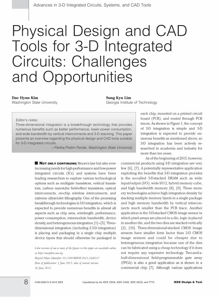
traces. As shown in Figure 1, the concept
of 3-D integration is simple and 3-D
integration is expected to provide nu-
merous benefits as mentioned above, so
3-D integration has been actively re-
searched in academia and industry for
more than ten years.
As of the beginning of 2015, however,
commercial products using 3-D integration are very
few [6], [7]. A potentially representative application
exploiting the benefits that 3-D integration provides
is the so-called 3-D-stacked DRAM such as wide
input/output (I/O), wide I/O 2, hybrid memory cube,
and high bandwidth memory [8], [9]. These mem-
ory technologies achieve high integration density by
stacking multiple memory layers in a single package
and high memory bandwidth by vertical intercon-
nects much smaller than the PCB trace. Another
application is the 3-D-stacked CMOS image sensor in
which pixel arrays are placed in a die, logic is placed
in another die, and the two dies are stacked vertically
[2], [10]. Three-dimensional-stacked CMOS image
sensors have smaller form factor than 2-D CMOS
image sensors and could be cheaper due to
heterogeneous integration because one of the dies
can be fabricated using a cheap technology if it does
not require any expensive technology. Two-and-a-
half-dimensional field-programmable gate array
(FPGA) is also a good application as is shown in a
commercial chip [7]. Although various applications
Editor’s notes:Three-dimensional integration is a breakthrough technology that providesnumerous benefits such as better performance, lower power consumption,and wide bandwidth by vertical interconnects and 3-D stacking. This paperpresents an overview regarding the physical design and CAD tools suitablefor 3-D integrated circuits.
VPartha Pratim Pande, Washington State University
IEEE Design & Test2168-2356/15 B 2015 IEEE Copublished by the IEEE CEDA, IEEE CASS, IEEE SSCS, and TTTC8
Advances in 3-D Integrated Circuits, Systems, and CAD Tools
Color versions of one or more of the figures in this paper are available online
at http://ieeexplore.ieee.org.
Digital Object Identifier 10.1109/MDAT.2015.2440317
Date of publication: 2 June 2015; date of current version:
30 June 2015.

have been suggested in academia and industry, these
are theonly representative applications realizable in the
very near future.
The delay of adoption of 3-D integration in the
mainstream semiconductor market might be due to
various reasons such as the lack of applications,
limitations that 3-D integration inherently has (such
as higher heat density), and the lack of standards and
computer-aided design (CAD) tools supporting 3-D
integrated circuits and systems. In this paper, we review
four different 3-D integration technologies: 2.5-D
integration, through silicon via (TSV) based, inductive
coupling based, and monolithic 3-D integration. Then,
we discuss challenges to overcome for adoption of 3-D
integration in the mainstream semiconductor market.
We also present uncharted design and optimization
problems to solve for the design of 3-D ICs.
Three-dimensional integrationtechnology
In this section, we review and discuss four 3-D
integration technologies (2.5-D, TSV-based 3-D,
inductive-coupling-based 3-D, and monolithic 3-D)
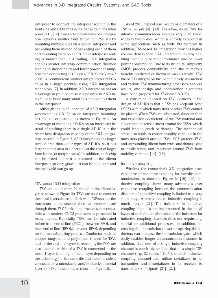
shown in Figure 2.
Two-and-a-half-dimensional integrationIn silicon interposer-based 3-D integration (name-
ly 2.5-D integration), multiple chips are mounted on
a silicon interposer and communicate through inter-
poser routing as shown in Figures 1 and 2a. Through
silicon vias (TSVs) are fabricated inside the silicon
Figure 1. Two-and-a-half-dimensional integration.
Figure 2. Four representative 3-D integration technologies: (a) 2.5-D; (b) TSV-based 3-D; (c) inductivecoupling-based 3-D; and (d) monolithic 3-D.
July/August 2015 9
interposer to connect the interposer routing in the
front side and C4 bumps in the backside of the inter-
poser [11], [12]. Two-and-a-half-dimensional integra-
tion achieves smaller form factor than 2-D ICs by
mounting multiple dies on a silicon interposer and
packaging them instead of packaging each of them
and mounting them on a PCB. Since interposer rout-
ing is smaller than PCB routing, 2.5-D integration
enables shorter interchip communication distance
leading to shorter delay and lower power consump-
tion than connecting 2-D ICs on a PCB. Xilinx Virtex-7
2000T is a commercial product integrating four FPGA
chips in a single package using 2.5-D integration
technology [7]. In addition, 2.5-D integration has an
advantage in yield because it is possible in 2.5-D in-
tegration to build many small dies and connect them
in the interposer.
Although the initial concept of 2.5-D integration
was mounting 2-D ICs on an interposer, mounting
3-D ICs is also possible, as shown in Figure 1. An
advantage of mounting 3-D ICs on an interposer in-
stead of stacking them in a single 3-D IC is in the
better heat dissipation capacity of the 2.5-D integra-
tion. As seen in Figure 2, 2.5-D integration has larger
surface area than other types of 3-D ICs, so it has
larger contact area to a heat sink at the cost of larger
form factor (or footprint area). In addition, each chip
can be tested before it is mounted on the silicon
interposer, so only good dies can be mounted and
the total yield can go up.
TSV-based 3-D integrationTSVs are conductors fabricated in the silicon la-
yer, as shown in Figure 2b. TSVs are used to connect
themetal layers above and below the TSVs so that the
transistors in the stacked dies can communicate
through them. TSV fabrication processes are compa-
tible with modern CMOS processes as presented in
many papers. Especially, TSVs can be fabricated
before front-end-of-line (FEOL), between FEOL and
back-end-of-line (BEOL), or after BEOL depending
on the manufacturing process. Conductor such as
copper, tungsten, and polysilicon is used for TSVs
and barrier and liner layers surrounding the TSVs are
also created. A side of a TSV is connected to the
metal 1 layer (or a higher metal layer depending on
the technology) in the same die and the other side is
connected to a microbump and/or a backside metal
layer for 3-D connections, as shown in Figure 2b.
As of 2015, typical size (width or diameter) of a
TSV is 1–5 �m [4], [13]. Therefore, using TSVs for
interdie communication enables very high band-
width between dies, which is actively exploited in
some applications such as wide I/O memory. In
addition, TSV-based 3-D integration provides higher
volume density than 2.5-D integration, thereby ena-
bling potentially better performance and/or lower
power consumption. Due to its structural simplicity,
CMOS process compatibility, and the numerous
benefits predicted or shown in various works, TSV-
based 3-D integration has been actively researched
and various TSV manufacturing processes, analysis
results, and design and optimization algorithms
have been proposed for TSV-based 3-D ICs.
A constraint imposed on TSV locations in the
design of 3-D ICs is that a TSV has keep-out zone
(KOZ) within which transistors or other TSVs cannot
be placed. When TSVs are fabricated, different ther-
mal expansion coefficients of the TSV material and
silicon induce tensile stress around the TSVs, which
could lead to crack or damage. The mechanical
stress also leads to carrier mobility variation in the
transistors placed around TSVs. KOZ protects TSVs
and surrounding silicon from crack and damage due
to tensile stress, and transistors around TSVs from
mobility variation [14]–[18].
Inductive couplingWireless (or contactless) 3-D integration uses
capacitive or inductive coupling for interdie com-
munication, as shown in Figure 2c [19], [20]. In-
ductive coupling shows many advantages over
capacitive coupling because the communication
distance of capacitive coupling is limited to a very
short range whereas that of inductive coupling is
much longer [21]. The inductors in inductive
coupling channels are implemented in the metal
layers of each die, so fabrication of the inductors for
inductive coupling channels does not require any
special or additional processes. In addition, in-
creasing the transmission power or upsizing the in-
ductors can increase the transmission gain, which
easily enables longer communication distance. In
addition, data rate of a single inductive coupling
channel is much higher than that of a single TSV
channel (e.g., 32 versus 1 Gb/s), so each inductive
coupling channel can utilize serializers in its
transmitter and deserializers in its receiver to
transmit a set of signals [21], [22].
IEEE Design & Test10
Advances in 3-D Integrated Circuits, Systems, and CAD Tools
Three-dimensional integration based on induc-
tive coupling provides a few advantages over TSV-
based or monolithic 3-D integration. Above all,
inductive coupling naturally enables heterogeneous
3-D integration. In detail, the inductive coupling
channels do not require any additional circuits for
interdie communication, so multiple dies operating
under different supply voltage values can naturally
communicate with each other through the channels.
However, interdie communication in TSV-based 3-D
ICs requires level shifters in the same situation,
which restricts the applicability of TSV-based 3-D ICs
to heterogeneous 3-D integration. Since inductive
coupling channels are free from voltage level
conversion, they provide much higher flexibility in
the design of heterogeneous 3-D ICs and systems.
Inductive coupling channels also naturally coex-
ist with microfluidic channels, which are considered
a very promising cooling solution for 3-D ICs, be-
cause inductors and microfluidic channels are
implemented in metal layers and silicon layers,
respectively. Therefore, microfluidic channels in the
inductive-coupling-based 3-D ICs are much easier to
design and can effectively spread heat. On the other
hand, TSVs and microfluidic channels interfere with
each other because both of them are fabricated in
the same silicon layer. Thus, design of 3-D ICs with
microfluidic channels and TSVs requires sophisti-
cated CAD algorithms to find optimal locations of
TSVs and microfluidic channels without sacrificing
performance and power consumption.
Monolithic 3-D integrationMonolithic 3-D integration stacks multiple, very
thin silicon layers, so it is expected to provide themost
fine-grained 3-D integration, as shown in Figure 2d.
Monolithic 3-D ICs can be built by various methods. A
way of stacking multiple thin layers is to fabricate a
bottom layer and deposit a new silicon layer on top
of the bottom layer. For example, Shenet al., [23] use
amorphous silicon (a-Si) deposition, green nanosec-
ond laser spike annealing (GN–LSA) crystallization,
and low-temperature thinning to form a new silicon
layer (so, thismethod is actually not stacking the layers
but fabricating the layers sequentially). On the other
hand, two separate layers can be fabricated separately
and stacked and one of them can be thinned. For
instance, monolithic 3-D RCAT flow by monolithic
IC3D [24] stacks the second layer onto the first (base)
layer and cuts the thick body of the second layer out
by ion-cut cleave, which is followed by gate formation
and metallization. In any case, the additional layers
are very thin (100–200 nm), so the vertical height of
interlayer vias is very short. Therefore, the parasitic
resistance and capacitance of an interlayer via are
almost negligible. The negligible parasitic resistance
and capacitance (RC) and the very tiny size of the
monolithic interlayer vias (MIVs) enable themost fine-
grained 3-D integration, potentially the largest amount
of performance improvement and power reduction,
and the smallest form factor.
Challenges and opportunitiesAlthough a huge amount of research effort has
been put on design and test methodologies, optimi-
zation algorithms, modeling, and analysis for 3-D
ICs, there are still fundamental challenges and new
issues to resolve for adoption of 3-D ICs in the main-
stream semiconductor market. In this section, we
discuss challenges and issues in 3-D integration.
ApplicationsThree-dimensional integration has disadvantages
such as higher heat density, more difficult testability,
and more expensive manufacturing cost, so the
amount of benefits that each application obtains
from 3-D integration should be sufficiently large. As
of 2015, however, applications that can fully exploit
the benefits that 3-D integration provides are very
limited, so finding more killer applications for 3-D
integration is one of the most important and chal-
lenging works for successful commercialization of
the 3-D integration technologies.
Bandwidth. The 3-D-stacked memory benefits from
very wide memory bandwidth are enabled by very
small interlayer vias [4], [25]–[27]. For instance, the
numbers of signal interlayer vias in [25], [26], and
[4] are 821, 32 768, and 7424, respectively. In the
same way, integrating multiple chips into a single 3-D
IC can replace PCB traces connecting the chips by
interlayer vias, thereby achieving very high die-to-die
(chip-to-chip) bandwidth. However, ‘‘What applica-
tions require the very high bandwidth?’’ is still an
open question. The wide I/O is a good example, but
just one application is not enough for commercial-
ization. A potential application in this area is integrat-
ingmany cores (e.g., network-on-chip) in a single 3-D
IC [4], [28], otherwise a subset of the cores should
be packaged in each chip and the chips should be
July/August 2015 11

connected on a PCB, which would have much lower
performance than the 3-D IC. In addition, if too many
intercore connections are required, the system may
not be physically realizable. Thus, 3-D integration
would be the only realizable technology for those
applications.
Power consumption. To achieve significant power
consumption by 3-D integration, several open ques-
tions should be answered, such as the following.
1) What chips should be stacked to benefit from I/O
power reduction?
2) What chips should be redesigned in 3-D to re-
duce power by wirelength reduction and short-
ened clock tree?
3) How can we develop CAD algorithms to reduce
wirelength?
Driving PCB traces consumes a huge amount of
power for their large capacitance, but stacking mul-
tiple chips in a 3-D IC and communicating through
low-parasitic interlayer vias can significantly reduce
the I/O power consumption. The 3-D-stacked
memory is a good example. In [4], the whole chip
composed of cores and memories consumes ap-
proximately 3.8 W. However, if the core and memory
dies are packaged separately and connected
through PCB traces, the power consumption only
for I/O would be approximately 4.0 W, assuming all
the signal I/O pads (in total, 7424 interdie signals) in
both the core and memory chips switch every clock
cycle, and the total power would be approximately
8 W, which is twice the power consumption of the
3-D chip. Therefore, the 3-D-stacked memory signifi-
cantly reduces power consumption by replacing
PCB traces and I/O cells by interlayer vias. Similarly,
Xilinx showed that integrating four FPGA chips in a
single package reduced power consumption from
112 to 19 W [7].
Another way to reduce power consumption is to
redesign a 2-D IC in 3-D. Redesigning a chip in 3-D
can shorten the logic and clock wires and remove
some buffers, thereby reducing dynamic power con-
sumption [29], [30]. However, the amount of power
reduction shown in the papers is not sufficiently
large for commercialization. For instance, the inter-
connect power of modern VLSI chips occupies
20%–30% of the total power consumption [30], [31].
Assuming the interconnect power is 30% of the total
power consumption and the interconnect power is
proportional to the interconnect length for simple
approximation, shortening the total interconnect
length by 30% and 50% reduces the total power
consumption by 9% and 15%, respectively. In reality,
Thorolfsson et al., [29] reduced the total wire length
by 56.9%, but the total power reduced only by
4.4% by 3-D integration using 180-nm technology
and 2.5-�m-diameter TSVs. Panthet al., [30] reduced
the total interconnect length by 20% and achieved
15.57% total power reduction by monolithic 3-D in-
tegration at 28 nm. In the latter, all the cell power, net
power, and leakage power reduced and contributed
to the total power reduction.
Stacking more dies in a single 3-D IC is another
way to shorten signal and clock wires, thereby re-
ducing dynamic power consumption. In [32], for
example, the wirelength of a specific benchmark is
minimizedwhen it is designed in five dies. Therefore,
more noticeable power reduction could be achieved
by stacking more dies [3]. However, stacking more
dies generally requires insertion of more interlayer
vias. Thus, if the parasitic RC of interlayer vias are not
negligible or inserting more interlayer vias causes
serious area overhead (e.g., inductors for inductive
coupling), stacking more dies might not reduce
dynamic power consumption sufficiently.
Form factor. The 3-D-stacked CMOS image sensor
places image sensors on a die and processing logic
on another die and stacks them in 3-D, thereby
achieving smaller form factor than the traditional 2-D
CMOS image sensor [33], [34]. For instance,
Suntharalingam et al., [33] stack seven layers con-
sisting of two 3-D image layers and five supporting
layers, and Lee et al., [34] stack three layers consist-
ing of an image sensor layer and two supporting
layers, thereby reducing the form factor significantly.
A common feature found in these works is that the
stacked layers are highly independently modular-
ized. The two main supporting layers in [33] are the
master and slave analog–digital converter (ADC)/
control layers. Similarly, the two layers under the
image sensor layer in [34] are the correlated double
sampling and ADC layers. Since the systems are
easily partitionable and the number of interlayer
connections is not many (in total, 336 in [33]), the
3-D-stacked CMOS image sensor is a good example
for achieving smaller form factor by 3-D integration.
However, just an application is not enough for
IEEE Design & Test12
Advances in 3-D Integrated Circuits, Systems, and CAD Tools
successful commercialization of 3-D integration and
‘‘What applications are easily partitionable into
balanced area?’’ is still an open question.
A potential application in this area is splitting a
multicore chip into multiple core andmemory layers
and stacking them as shown in [4] and [35] as long
as the number of connections among them is not
many. This application is easily partitionable be-
cause the cores and thememory blocks are indepen-
dently modularized. The simple connectivity plays
an important role in the physical design step because
it enables manual physical design (partitioning and
placement of the partitioned modules and interlayer
vias). If the connectivity is complex, however, CAD
tools would be required to automatically place the
submodules and interlayer vias.
Performance. Performance benefits can be ob-
tained in several ways. For instance, the wide I/O
improves performance by loading a large memory
block in a short period using the wide memory
bandwidth. In this case, the direct benefit of 3-D in-
tegration is achieving the wide bandwidth between
dies, but the ultimate benefit is the performance im-
provement [26]. On the other hand, Saito et al., [25]
achieve 43% latency reduction by reorganizing
memory elements, which leads to performance im-
provement of the system. Performance improvement
can also be obtained by redesigning 2-D ICs in 3-D.
Thorolfsson et al., [29] achieved 19.7% critical path
delay reduction, and Kim et al., [32] also achieved
20%–50% critical path delay reduction by redesign-
ing in two layers. Lee et al., [36] showed that mono-
lithic 3-D ICs achieved even better timing than
TSV-based 3-D ICs. Redesigning 2-D ICs in 3-D re-
duces the footprint area, so the total wirelength goes
down and the critical path delay is improved. Thus,
it achieves both smaller form factor and perfor-
mance improvement.
However, ‘‘What chips can be redesigned in 3-D to
maximize performance?’’ and ‘‘How can we improve
performance?’’ are still open questions. Performance
could be improved by: 1) increased operation fre-
quency achieved by reducing critical path delay;
2) increased throughput achieved by increasing
communication bandwidth and integrating more
processing elements; and 3) improved architectures
enabled by 3-D integration [37]. Unfortunately,
improving performance by 3-D integration in many
cases requires very effective and efficient CAD algo-
rithms, which are not mature yet. We will discuss CAD
tools for 3-D integration in the CAD tools section.
Thermal issuesThree-dimensional ICs have higher device densi-
ty than 2-D ICs, so heat dissipation per unit volume is
higher than that of 2-D ICs. In addition, dies seating in
themiddle of a 3-D IC have longer heat path to the top
and bottom heat sinks and higher heat coupling with
neighboring dies than the dies on the boundary
close to the heat sinks. This heat dissipation and
thermal coupling problem is translated into the in-
crease of the maximum and average temperature, so
3-D ICs are more vulnerable to thermal problems
than 2-D ICs, which is a major bottleneck for adop-
tion of 3-D ICs.
Two-and-a-half-dimensional integration of 2-D ICs
has the lowest heat coupling compared to the other
3-D integration methodologies because heat dis-
sipation per unit surface area does not increase.
However, lateral heat coupling exists among the in-
tegrated 2-D dies in 2.5-D integration. Temperature in
2.5-D integration highly depends on the interposer
material, as shown in [38], but the other 3-D integra-
tion technologies have more serious thermal issues
than 2.5-D integration. Heat coupling in TSV- and
inductive-coupling-based 3-D integration signifi-
cantly increases the temperature. In addition, mono-
lithic 3-D integration has the highest device density
per volume among all the 3-D integration technolo-
gies. Assuming all the transistors in different tiers
have the same characteristics [39], heat coupling in
two-tier and three-tier monolithic 3-D ICs have ap-
proximately 10 �C and 25 �C higher maximum tem-
perature than 2-D ICs, respectively [40].
To reduce the temperature and distribute heat
effectively, various cooling and optimization method-
ologies have been proposed. One of themost effective
cooling techniques is the microfluidic cooling (MFC).
MFC inserts microfluidic channels carrying cooling
fluid into the siliconbulk so that the silicon substrate is
cooled down by the cooling fluid. However, micro-
fluidic channels are inserted into the silicon bulk, so
they overlap with TSVs. Due to this, the design of
TSV-based 3-D ICs with MFC requires sophisticated
design and optimization algorithms [41], [42]. On the
other hand, inductive links and silicon bulk do not
overlap in inductive-coupling-based 3-D ICs.
Various design-level optimization algorithms
have also been proposed to resolve the heat problem.
July/August 2015 13
Via planning such as thermal via insertion and TSV
alignment spreads heat more effectively just by
increasing the heat conductivity of the whole 3-D
chip [43]–[45]. Optimization of cell locations during
placement can also reduce temperature [46], [47].
CAD toolsPhysical design of 3-D ICs requires new tools for
design, analysis, and optimization. In this section, we
discuss uncharted problems to solve for successful
commercialization of each 3-D integration technology.
Two-and-a-half-dimensional integrationEnabling 2.5-D integration requires floorplanning
on a silicon interposer and routing through the in-
terposer. Although the dies are located on top of the
interposer and the routing layers are inside the inter-
poser, routing of the 2.5-D ICs is similar to that of 2-D
ICs because flipping the 2.5-D ICs leads to the same
routing structure, i.e., the routing layers exist on top
of the pins. On the other hand, floorplanning for
2.5-D integration is a bit different from that for 2-D
ICs. If 2.5-D integration places 2-D dies on a silicon
interposer, floorplanning of the 2-D dies is almost
the same as the 2-D floorplanning problem that
places 2-D modules on a die.
However, floorplanning of 2-D and 3-D dies across
the chips placed on a silicon interposer has not been
investigated. As Figure 1 shows, real 3-D floorplan-
ning for 2.5-D integration requires determining the
number of 2-D and 3-D dies to mount on a silicon
interposer, the locations of the dies, and the loca-
tions of the modules in each die. In the figure: 1) six
dies are to be placed and two of them are 2-D ICs,
another two of them are two-die 3-D ICs, and the
other two are three-die 3-D ICs; 2) the locations of
the ICs on the silicon interposer are to be
determined; and 3) the locations of all the modules
integrated in the 2.5-D IC are to be optimized.
Definitely the objective function should include
wirelength, routability, performance, and tempera-
ture. Especially, the routability includes not only
intra-IC routability but also inter-IC routability. For
instance, placing two modules having many con-
nections between them in two different chips needs
as many microbump pins as the connection count.
Therefore, poorly placed modules in 2.5-D ICs will
increase the total wirelength and result in unrou-
table designs. Therefore, 3-D floorplanning for the
design of 2.5-D ICs should consider all the metrics
while achieving 100% routability. Thermal-aware 3-D
floorplanning algorithms for 2.5-D integration should
also be developed for more effective heat dissipation
in 2.5-D ICs. The temperature models presented in
[48] and [49] or the temperature optimization
methodology used in [50] could be applied to
temperature analysis and optimization of 2.5-D ICs.
However, intrachip and interchip thermal conduc-
tivities could be very different, so more accurate
thermal analysis and models for 2.5-D ICs and
effective thermal-aware 2.5-D floorplanning algo-
rithms need to be developed.
TSV-based 3-D integrationTSV-based 3-D integration has been one of the
most promising 3-D integration technologies, so a
large amount of efforts has been spent to develop
design and analysis methodologies and optimiza-
tion algorithms for TSV-based 3-D ICs.
Three-dimensional floorplanning. Three-dimen-
sional floorplanning of TSV-based 3-D ICs optimizes
the locations of the blocks in a given netlist in 3-D.
Each block could be a 2-D or 3-D block, and a hard
constraint is that any two blocks should not overlap
horizontally and vertically. Three-dimensional out-
lines (width, height, and vertical length of the target
3-D floorplan) can also be given as a hard constraint.
The objective function should include wirelength,
the volume of the 3-D floorplan, performance, tem-
perature, and so on. Differently from 2-D floorplan-
ning, however, 3-D floorplanning for TSV-based 3-D
ICs should also consider TSV insertion, as shown in
[51]–[53]. Unfortunately, TSV insertion is a chicken-
and-egg problem because optimizing TSV locations
requires the locations of the blocks, but optimiza-
tion of the block locations should consider TSV lo-
cations. If 3-D floorplanning does not consider TSV
locations, many 3-D nets may need detours that will
lead to wirelength overhead. According to [52], 3-D
floorplanning needs to consider block locations,
TSV locations, 3-D routing, and whitespace manip-
ulation, all at the same time to optimize the objective
function. Since some blocks occupy large area or
volume, adjusting the locations of the blocks could
significantly affect the total wirelength. In addition,
the number of TSVs should also be controlled care-
fully to minimize the area overhead for TSV inser-
tion. For this purpose, multilayer obstacle-avoiding
rectilinear Steiner minimum tree (MLOARSMT)
IEEE Design & Test14
Advances in 3-D Integrated Circuits, Systems, and CAD Tools
construction algorithms should be developed. The
wirelength reduction reported in [52] is 7%–38% for
three-die designs and 9%–34% for four-die designs,
but more effective algorithms should be developed
for adoption of 3-D integration.
Similarly to 2-D floorplanning, more various
3-D floorplanning problems exist for more flexible
and useful 3-D floorplanning. Two representative 3-D
floorplanning problems are exploiting soft 3-D
blocks and bufferable 3-D blocks as those for 2-D
floorplanning [54]–[57]. Soft 3-D blocks have varia-
ble dimensions (width, height, and vertical length)
with a range of volume instead of fixed dimensions.
However, the vertical length is discretized because it
is integer multiples of the thickness of a die, assum-
ing all the dies have the same thickness. Bufferable
3-D blocks allow CAD tools to insert buffers and TSVs
into the blocks so that CAD tools can avoid long de-
tours during 3-D routing. All of these 3-D floor-
planning problems have not been investigated yet.
Three-dimensional placement. Three-dimensional
placement optimizes the locations of the standard
cells in a given netlist in 3-D. Three-dimensional
placement is fundamentally the same as 3-D floor-
planning of 2-D blocks because both of them
optimize the locations of the placeable objects
(cells and blocks) in multiple dies. However, per-
turbing a small area to insert TSVs in 3-D placement
does not degrade the total wirelength significantly,
so TSV insertion in 3-D placement can be performed
after cells are placed. However, performing 3-D
placement and TSV insertion at the same time would
generate better layouts. The wirelength reduction
achieved by four-die designs in [32] is 1%–25% and
that in [46] is less than that in [32]. In addition to the
wirelength reduction, critical path delay can also be
reduced by 3-D integration. The critical path delay
reduction achieved by two-die designs in [58] is
approximately 10%.
Since heat dissipation is one of the most im-
portant issues to be solved in 3-D integration,
thermal-aware 3-D placement algorithms have been
developed. Luo et al., [46] and Athikulwongse et al.,
[47] investigated effective heat distribution by
analytically optimizing cell and TSV locations.
Unfortunately, thermal optimization during 3-D
placement degrades wirelength. Therefore, much
more effective 3-D placement algorithms that can
simultaneously optimize wirelength and tempera-
ture should be developed for adoption of TSV-based
3-D integration.
Three-dimensional routing. Routing of 3-D ICs
does not require any new algorithms once TSV loca-
tions are found because routing after TSV insertion
can be performed in each die separately. However,
TSVs can also be inserted during routing after place-
ment. Three-dimensional routing can be performed
by two existing routing algorithms, multilayer global
routing algorithms, and multilayer obstacle-avoiding
rectilinear Steiner tree (MLOARST) algorithms [59].
The former collapses routing resources onto a 2-D
plane, performs 2-D global routing, and expands the
routing result back to 3-D by layer assignment. To
apply this algorithm to 3-D routing, the 2-D global
routing and the layer assignment algorithms need to
consider the number of TSVs to insert and their lo-
cations. On the other hand, the MLOARSTalgorithms
handle placement blockages and 3-D routing, so
they are more suitable for 3-D routing. However, the
runtime of the MLOARST algorithms is long in gene-
ral. A more optimal algorithm than the MLOARST
algorithms for 3-D routing would be an MLOARSMT
algorithm, which has not been investigated in the
literature yet.
Three-dimensional clock tree synthesis. A sim-
ple 3-D clock tree synthesis (CTS) algorithm con-
structs a 2-D clock tree in each die and connects the
source points through TSVs considering the parasitic
RC of the TSVs. This 3-D CTS utilizes the minimum
number of TSVs, but its wirelength would not be the
shortest. On the other hand, utilizing more TSVs
could reduce the wirelength further at the cost of
TSVs [60]. Although the wirelength is of primary
concern in 3-D CTS, prebond and postbond testabil-
ity is also an important issue in 3-D CTS for yield
improvement [61], [62]. Especially, the prebond-
and postbond-testability-aware 3-D CTS should
minimize the wirelength of the 2-D clock tree
constructed for prebond test in each die, that of
the whole 3-D clock tree, skew of both 2-D and 3-D
trees, and power consumption (and the TSV count
depending on the TSV cost).
One of the existing issues in 3-D CTS is whether a
3-D clock tree constructed for a 3-D IC consumes less
power than the 2-D clock tree constructed in its 2-D
counterpart IC. Power reduction in 3-D integration
can also be obtained if the 3-D clock tree has shorter
July/August 2015 15

wirelength than the 2-D clock tree. However, the
wirelength of the 3-D clock trees shown in [63] is
longer than that of the 2-D clock trees by 33%–46%.
Moreover, the actual power consumption of the 3-D
clock tree is dependent on both the wirelength and
the TSV capacitance. Therefore, even if the planar
wirelength of the 3-D clock tree is shorter than that of
the 2-D clock tree, the 3-D clock tree might consume
more power than the 2-D clock tree. Therefore, 3-D
CTS algorithms should also take the TSV count into
account to minimize the power consumption of the
3-D clock trees.
Three-dimensional power network design. Powerin TSV-based 3-D ICs can be delivered from the
bottommost die (assuming the bottommost die is
connected to I/O cells) to other dies through power/
ground (P/G) TSVs on the chip boundary and/or P/G
TSVs in the core area. In any case, signal TSVs in the
core area interfere with P/G lines and stripes, so 3-D
P/G network design for TSV-based 3-D ICs needs to
handle the discontinuity of P/G lines and stripes
around signal TSVs. If the height of a TSV is greater
than that of a standard cell row, TSVs should be
treated as small IPs, so small P/G rings should be
inserted around each TSV to guarantee the conti-
nuity of P/G lines and stripes. This task could be
simplified by designing a signal TSV cell in which P/G
rings are contained. In this case, P/G routing should
be performed after placement. If TSV locations are
changed during any design step, however, P/G
routing should be reperformed in the layout area
modified.
IR drop in TSV-based 3-D ICs is expected to be
smaller than that in 2-D ICs due to smaller footprint
area. However, P/G TSV insertion inside the core area
can help reduce the IR drop further, so minimizing
the number of P/G TSVs satisfying IR drop constraints
has been researched in several works [64]–[66].
Ldi/dt noise can also be optimized [64], [67] by
optimization of P/G TSV locations.
Inductive-coupling-based 3-D integrationA fundamental difference between an inductive
coupling channel and a TSV is that the inductive
coupling channel has much higher data rate than a
TSV, so transmitting and receiving digital signals
through an inductive coupling channel can use se-
rializers anddeserializers to fully utilize the data rate.
In this case, serialization and deserialization of
multiple nets require that either the initial netlist
should contain serializers and deserializers or the
design software can insert them into the netlist con-
sidering the cell and block locations. This is a new,
unique constraint or task existing in the design of
inductive-coupling-based 3-D ICs.
Three-dimensional floorplanning. Three-dimen-
sional floorplanning for inductive-coupling-based
3-D ICs is similar to that for TSV-based 3-D ICs.
However, there are fundamental differences between
these two 3-D floorplanning problems. In the induc-
tive-coupling-based 3-D ICs, two inductive links that
belong to different nets should not overlap vertically
so that the links do not interfere with each other. This
nonoverlap condition is a unique constraint existing
in the 3-D floorplanning of inductive-coupling-based
3-D ICs. Due to this new constraint, each 3-D hard
block should have the locations of the inductive links
in it as input to the 3-D floorplanning so that 3-D
floorplanning can avoid aligning inductors belonging
to different nets. In addition, the number of inductive
links to insert and their locations should also be
considered and/or determined during 3-D floorplan-
ning because the inductive links should be placed in
whitespace similarly to TSVs. Moreover, the data rate
of an inductive link is higher than that of a TSV, so
multiple nets can share a single inductive link by
utilizing serializers and deserializers. In this case,
multiple signals coming from different blocks can
share an inductive link placed in whitespace, so
assignment of signals to inductive links also becomes
an issue in the 3-D floorplanning for inductive-
coupling-based 3-D ICs. However, none of these
subjects have been investigated yet.
Three-dimensional placement and 3-D rou-ting. Three-dimensional placement for inductive-
coupling-based 3-D ICs needs to place inductive
links, which can be handled similarly to the TSVs in
the TSV-based 3-D ICs. However, there are also funda-
mental differences between them. First, an inductive
link is much larger than a TSV. For instance, the
inductor size ranges between 30 �m� 30 �m and
150 �m� 150 �m, depending on the communica-
tion distance (die thickness) [21], whereas the TSV
size ranges between 1 �m� 1 �m and 5 �m� 5 �m,
depending on the TSV technology. Therefore, plac-
ing cells and inductive links is similar to the 3-D
mixed-size placement problem rather than the 3-D
IEEE Design & Test16
Advances in 3-D Integrated Circuits, Systems, and CAD Tools
gate-level placement. In addition, if it is allowed to
reassign 3-D nets to inductive links, as shown in
Figure 3, 3-D placement algorithms should be able
to consider the reassignment before/during/after
3-D placement, which is a completely new problem.
Another constraint uniquely existing in the 3-D
placement of inductive-coupling-based 3-D ICs is
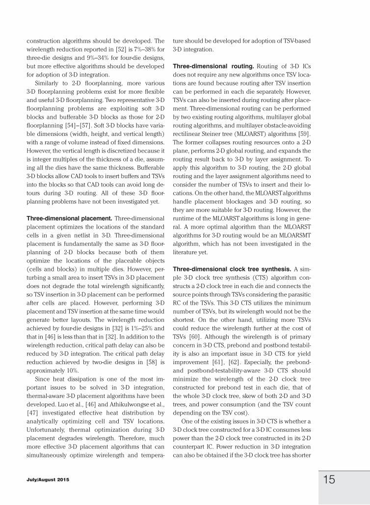
that cells should not be placed between two induc-
tors vertically aligned in multidie (more than two
dies) 3-D ICs. For instance, cells cannot be placed at
the samex- andy-locations as the two inductors
placed in die 1 and die 3 for an inductive link, as
shown in Figure 4. Thus, the area between two in-
ductors vertically aligned is wasted. A way to avoid
this wasted area is to place another inductor in the
middle of them so that the three inductors form a
single inductive channel. This multidie inductive
link can be used to broadcast a signal from a die to
multiple dies and is useful for the 3-D nets connect-
ing cells placed in multiple dies. However, if only a
few 3-D nets connect cells in die 1 and die 2 through
an inductive link and some other nets connect cells
in die 1 and die 3 through the same inductive link, it
actually wastes the resources.
Once the locations of cells and inductive links in
a 3-D IC are finalized, each die in the 3-D IC can be
routed independently. However, if reassignment of
the 3-D nets to inductive links is allowed during
routing, more sophisticated algorithms for the net-to-
link reassignment and the construction of a multi-
layer rectilinear Steiner minimum tree (MLRSMT)
considering the locations of the preplaced inductive
links should be developed and used. Several differ-
ent 3-D routing algorithms such as sequential rout-
ing of 3-D nets and concurrent routing of 3-D nets
could be developed and actual routing of inductive-
coupling-based 3-D ICs will need to consider wire-
length, timing, distribution of available inductive
links, and reassignment of inductive links, which has
not been investigated yet at all.
Three-dimensional clock tree synthesis. Al-though 3-D CTS for inductive-coupling-based 3-D
ICs is similar to that for TSV-based 3-D ICs, the area
cost of an inductive link is more expensive than that
of a TSV. Therefore, inserting too many inductive
links is prohibitive, which leads to the minimization
of the number of inductive links used for 3-D CTS.
However, minimizing the number of inductive links
in a 3-D clock tree will not reduce the planar wire-
length of the 3-D clock tree. Rather, incorporating
the prebond testability with the minimization of the
inductive link count will likely increase the planar
wirelength of the 3-D clock tree, which will lead to
higher power consumption than the clock tree built
for 2-D ICs. No work exists on 3-D CTS for inductive-
coupling-based 3-D ICs, so more research on this
topic should be conducted for adoption of inductive-
coupling-based 3-D integration.
Three-dimensional power network design. Powerdelivery from the bottommost die to other dies in
inductive-coupling-based 3-D ICs is more challeng-
ing than that in TSV-based 3-D ICs. Depending on in
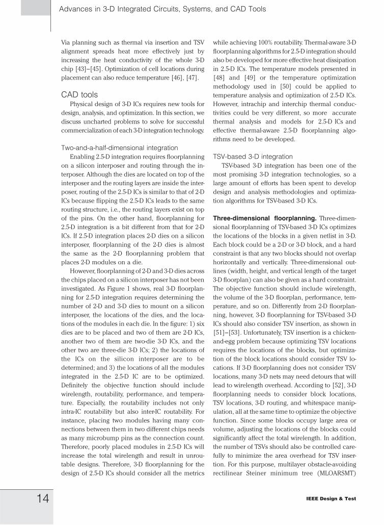
Figure 3. Assignment of 3-D nets toinductive links.
Figure 4. Placing cells betweentwo inductors is prohibited.
July/August 2015 17

which metal layer inductors are created, P/G lines
and stripes might need to detour the inductors. In
addition, delivering power through P/G inductors is
much less efficient than that through wire-bonding
or TSVs with respect to the area utilization and power
efficiency [68]–[72]. Thus, inserting P/G inductors
inside the core area is almost impractical. For power
delivery in inductive-coupling-based 3-D ICs, there-
fore, special-purpose TSVs are used in some applica-
tions [22].
Monolithic 3-D integrationAlthough TSVs and monolithic interlayer vias
(MIVs) have very different sizes (1–5 �m versus
0.1 �m), some of the design methodologies for TSV-
based could also be used for monolithic 3-D ICs.
Three-dimensional floorplanning. Three-dimen-
sional floorplanning for monolithic 3-D ICs could
be performed in two steps: 3-D floorplanning and
MIV insertion [73]. Differently from 3-D floorplan-
ning for TSV-based 3-D ICs in which TSV insertion
should be considered during 3-D floorplanning not
to cause any serious wirelength overhead in the final
TSV insertion step, 3-D floorplanning for monolithic
3-D ICs could perform 3-D floorplanning itself
without considering the locations of MIVs. This is
because MIVs are much smaller than TSVs, so MIV
insertion after 3-D floorplanning might not cause
serious wirelength overhead. However, 3-D routing
should still be considered during 3-D floorplanning
for wirelength minimization.
Most of the new 3-D floorplanning problems for
TSV-based 3-D ICs such as the two representative
3-D floorplanning problems (soft and bufferable 3-D
blocks) discussed in the section on TSV-based 3-D
integration also exist in the design of monolithic
3-D ICs. In addition, monolithic 3-D ICs have higher
power density than TSV-based 3-D ICs, so 3-D floor-
planning for monolithic 3-D ICs should optimize
heat removal much more effectively than that for
TSV-based 3-D ICs [40].
Three-dimensional placement. Three-dimen-
sional placement algorithms for TSV-based 3-D ICs
can also be used for monolithic 3-D ICs. A big
difference between them is that TSVs are large, so
the TSV count should be carefully controlled in the
design of TSV-based 3-D ICs. However, the size of an
MIV is similar to that of a local via, so the MIV count
may not need to be carefully controlled. For exam-
ple, when the die size is 1 mm� 1 mm, utilization is
70%, and the MIV size is 70 nm, the whitespace
existing in a layer of the layout can accommodate
approximately 15 million MIVs, which is almost infi-
nite. Thus, 3-D placement algorithms for monolithic
3-D ICs can first place cells without considering MIV
locations and then insert MIVs for each net during
routing. A 3-D placement algorithm for monolithic
3-D ICs is to use an existing 2-D placement tool with
uniform downscaling of cell locations and partition-
ing [30]. This design methodology preserves the
relative locations among the cells up to a certain
point, but does not guarantee optimality even if the
initial 2-D placement result is optimal. However, the
methodology is easy to use, so it could be used as a
baseline for comparison of 3-D placement algo-
rithms for monolithic 3-D ICs.
Three-dimensional placement for monolithic 3-D
ICs should also handle heat dissipation properly. Al-
though various design methodologies and algo-
rithms such as thermal via insertion and alignment
for heat dissipation have been developed for TSV-
based 3-D ICs [46], [47], there is almost no work on
thermal-aware 3-D placement algorithms for mono-
lithic 3-D ICs. For example, redundant MIV insertion
for efficient heat transfer and its relationship with
routing congestion has not been investigated yet.
Three-dimensional routing and clock tree syn-thesis. Three-dimensional routing for TSV-based
3-D ICs can also be used for monolithic 3-D ICs. Both
of them routes 3-D nets through multiple routing
layers. However, 3-D routing for monolithic 3-D ICs
might not need to control the MIV count because
MIVs are sufficiently small. In this sense, MLOARST
or MLOARSMT algorithms that can take the number
of MIVs into account should be developed so that
3-D routing for TSV-based 3-D ICs can minimize the
TSV count if the TSV size is large and 3-D routing for
monolithic 3-D ICs can use sufficiently many MIVs
while minimizing the total wirelength.
Three-dimensional CTS algorithms for monolith-
ic 3-D ICs might not need prebond testability unless
each tier can be tested during manufacturing. Al-
though a few 3-D CTS algorithms have been used in
the literature [30], more general and effective 3-D
CTS algorithms that can balance the MIV count and
the clock tree wirelength need to be developed to
reduce the clock power.
IEEE Design & Test18
Advances in 3-D Integrated Circuits, Systems, and CAD Tools

Three-dimensional power network design. Mo-
nolithic 3-D ICs have much higher cell density than
TSV-based or inductive-coupling-based 3-D ICs. Thus,
3-D P/G network in monolithic 3-D ICs has a larger
impact on the quality of the 3-D ICs than that in
TSV-based or inductive-coupling-based 3-D ICs [74].
Especially, monolithic 3-D ICs have higher routing
congestion than other types of 3-D ICs because of
the highest cell density, but MIV insertion has a little
impact on the quality of monolithic 3-D ICs. There-
fore, P/G network topology generation and optimiza-
tion algorithms for monolithic 3-D ICs should focus
on reducing routing congestion while satisfying IR
drop constraints.
AN ENORMOUS AMOUNT of effort has been put on
3-D integration to achieve better performance, lower
power consumption, and smaller form factor, but
adoption of 3-D integration in the high-performance
and/or low-power semiconductor market has been
delayed for several years. The delay of the adoption
is due to various reasons such as the lack of appli-
cations, limitations 3-D integration inherently has,
and the lack of standards and CAD tools. To expedite
adoption of 3-D integration, more killer applications
that can fully exploit the benefits that 3-D integration
provides should be developed. In addition, 3-D ICs
have more serious heat density problems than 2-D
ICs, so more effective heat distribution and removal
technologies and algorithms need to be developed.
The actual amount of benefits that the papers on the
design of 3-D ICs obtained is not satisfactory, so more
effective and efficient design methodologies and
optimization algorithms for 3-D ICs should also be
developed. h
h References[1] R. Weerasekera, D. Pamunuwa, L.-R. Zheng, and
H. Tenhunen, ‘‘Two-dimensional and three-dimensional
integration of heterogeneous electronic systems under
cost, performance, technological constraints,’’ IEEE
Trans. Comput.-Aided Design Integr. Circuits Syst.
vol. 28, no. 8, pp. 1237–1250, Aug. 2009.
[2] S.-F. Yeh, C.-C. Hsieh, and K.-Y. Yeh, ‘‘A 3 megapixel
100 Fps 2.8 um pixel pitch CMOS image sensor
layer with built-in self-test for 3D integrated
imagers,’’ IEEE J. Solid-State Circuits, vol. 48, no. 3,
pp. 839–849, Mar. 2013.
[3] D. H. Kim, S. Mukhopadhyay, and S. K. Lim,
‘‘TSV-aware interconnect distribution models for
prediction of delay and power consumption of 3-D
stacked ICs,’’ IEEE Trans. Comput.-Aided Design
Integr. Circuits Syst., vol. 33, no. 9, pp. 1384–1395,
Sep. 2014.
[4] D. H. Kim et al., ‘‘Design and analysis of 3D-MAPS
(3D massively parallel processor with stacked
memory),’’ IEEE Trans. Comput., vol. 64, no. 1,
pp. 112–125, Jan. 2015.
[5] C. Erdmann et al., ‘‘A heterogeneous 3D-IC consisting
of two 28 nm FPGA die and 32 reconfigurable
high-performance data converters,’’ IEEE J. Solid-State
Circuits, vol. 50, no. 1, pp. 258–269, Jan. 2015.
[6] Micron, ‘‘Hybrid memory cube.’’ [Online]. Available:
http://www.micron.com/products/hybrid-memory-cube.
[7] Xilinx, ‘‘2.5D ICs: Just a stepping stone or a long
term alternative to 3D.’’ [Online]. Available: http://www.
xilinx.com/innovation/research-labs/keynotes/3-D_
Architectures.pdf.
[8] JEDEC. [Online]. Available: http://www.jedec.org.
[9] Hybrid Memory Cube Consortium. [Online]. Available:
http://www.hybridmemorycube.org.
[10] J. Aoki et al., ‘‘A rolling-shutter distortion-free 3D
stacked image sensor with �160 dB parasitic light
sensitivity in-pixel storage node,’’ in Proc. IEEE Int.
Solid-State Circuits Conf., Feb. 2013, pp. 482–483.
[11] T. C. Chai et al., ‘‘Development of large die fine-pitch
Cu/low-k FCBGA Package with through Silicon via
(TSV) interposer,’’ IEEE Trans. Compon. Packag.
Manuf. Technol., vol. 1, no. 5, pp. 660–672,
May 2011.
[12] Q. Chen, Y. Suzuki, G. Kumar, V. Sundaram, and
R. R. Tummala, ‘‘Modeling, fabrication,
characterization of low-cost and high-performance
polycrystalline panel-based silicon interposer with
through vias and redistribution layers,’’ IEEE Trans.
Compon. Packag. Manuf. Technol., vol. 4, no. 12,
pp. 2035–2041, Dec. 2014.
[13] W. Guo et al., ‘‘Copper through silicon via induced
keep out zone for 10 nm node bulk FinFET CMOS
technology,’’ in Proc. IEEE Int. Electron Devices
Meeting, Dec. 2013, pp. 12.8.1–12.8.4.
[14] K. H. Lu et al., ‘‘Thermo-mechanical reliability of
3-D ICs containing through silicon vias,’’ in Proc.
IEEE Electron. Compon. Technol. Conf., May 2009,
pp. 630–634.
[15] C. S. Selvanayagam et al., ‘‘Nonlinear thermal
stress/strain analyses of copper filled TSV (through
silicon via) and their flip-chip microbumps,’’ IEEE
Trans. Adv. Packag., vol. 32, no. 4, pp. 720–728,
Apr. 2009.
July/August 2015 19
[16] K. Athikulwongse, A. Chakraborty, J.-S. Yang,
D. Z. Pan, and S. K. Lim, ‘‘Stress-driven 3D-IC
placement with TSV keep-out zone and regularity
study,’’ in Proc. IEEE Int. Conf. Comput.-Aided
Design, Nov. 2010, pp. 669–674.
[17] K. Athikulwongse, J.-S. Yang, D. Z. Pan, and
S. K. Lim, ‘‘Impact of mechanical stress on the full
chip timing for through-silicon-via-based 3-D ICs,’’
IEEE Trans. Comput.-Aided Design Integr. Circuits
Syst., vol. 32, no. 6, pp. 905–917, Jun. 2013.
[18] M. Jung, D. Z. Pan, and S. K. Lim, ‘‘Chip/package
mechanical stress impact on 3-D IC reliability and
mobility variations,’’ IEEE Trans. Comput.-Aided
Design Integr. Circuits Syst., vol. 32, no. 11,
pp. 1694–1707, Nov. 2013.
[19] N. Miura et al., ‘‘A 1 Tb/s 3 W inductive-coupling
transceiver for 3D-stacked inter-chip clock and data
link,’’ IEEE J. Solid-State Circuits, vol. 42, no. 1,
pp. 111–122, Jan. 2007.
[20] M. Saen et al., ‘‘3-D system integration of processor
and multi-stacked SRAMs using inductive-coupling
link,’’ IEEE J. Solid-State Circuits, vol. 45, no. 4,
pp. 856–862, Apr. 2010.
[21] Y. Take et al., ‘‘3D NoC with inductive-coupling
links for building-block SiPs,’’ IEEE Trans. Comput.,
vol. 63, no. 3, pp. 748–763, Mar. 2014.
[22] D. Ditzel, T. Kuroda, and S. Lee, ‘‘Low-cost 3D chip
stacking with thruchip wireless connections,’’ Hot
Chips, pp. 1–37, Aug. 2014.
[23] C.-H. Shen et al., ‘‘Monolithic 3D chip integrated
with 500 ps NVM, 3 ps logic circuits and SRAM,’’ in
Proc. IEEE Int. Electron Devices Meeting, Dec. 2013,
pp. 9.3.1–9.3.4.
[24] MonolithicIC3D. [Online]. Available: http://
monolithic3d.com.
[25] H. Saito et al., ‘‘A chip-stacked memory for on-chip
SRAM-rich SoCs and processors,’’ IEEE J. Solid-State
Circuits, vol. 45, no. 1, pp. 15–22, Jan. 2010.
[26] D. H. Woo, N. H. Seong, D. L. Lewis, and H.-H. S. Lee,
‘‘An optimized 3D-stacked memory architecture by
exploiting excessive, high-density TSV bandwidth,’’ in
Proc. IEEE Int. Symp. High-Performance Comput.
Architect., Jan. 2010, pp. 429–440.
[27] D. H. Woo, N. H. Seong, and H.-H. S. Lee, ‘‘Pragmatic
integration of an SRAM row cache in heterogeneous
3-D DRAM architecture using TSV),’’ IEEE Trans.
Very Large Scale Integr. (VLSI) Syst., vol. 21, no. 1,
pp. 1–13, Jan. 2013.
[28] B. S. Feero and P. P. Pande, ‘‘Networks-on-chip
in a three-dimensional environment: A performance
evaluation,’’ IEEE Trans. Comput., vol. 58, no. 1,
pp. 32–45, Jan. 2009.
[29] T. Thorolfsson, K. Gonsalves, and P. D. Franzon,
‘‘Design automation for a 3DIC FFT processor
for synthetic aperture radar: A case study,’’ in Proc.
ACM Design Autom. Conf., 2009, pp. 51–56.
[30] S. Panth, K. Samadi, Y. Du, and S. K. Lim, ‘‘Design
and CAD methodologies for low power gate-level
monolithic 3D ICs,’’ in Proc. Int. Symp. Low Power
Electron. Design, 2014, pp. 171–176.
[31] N. Magen, A. Kolodny, U. Weiser, and N. Shamir,
‘‘Interconnect-power dissipation in a microprocessor,’’
in Proc. ACM/IEEE Int. Workshop Syst. Level
Interconnect Prediction, Feb. 2004, pp. 7–13.
[32] D. H. Kim, K. Athikulwongse, and S. K. Lim, ‘‘Study
of through-silicon-via impact on the 3-D stacked IC
layout,’’ IEEE Trans. Very Large Scale Integr. (VLSI)
Syst., vol. 21, no. 5, pp. 862–874, May 2013.
[33] V. Suntharalingam et al., ‘‘A 4-side tileable back
illuminated 3D-integrated Mpixel CMOS image
sensor,’’ in Proc. IEEE Int. Solid-State Circuits Conf.,
Feb. 2009, pp. 38–39.
[34] K.-W. Lee et al., ‘‘Die-level 3-D integration
technology for rapid prototyping of high-performance
multifunctionality hetero-integrated systems,’’
IEEE Trans. Electron Devices, vol. 60, no. 11,
pp. 3842–3848, Nov. 2013.
[35] D. Fick et al., ‘‘Centip3De: A cluster-based NTC
architecture with 64 ARM Cortex-M3 Cores in
3D stacked 130 nm CMOS,’’ IEEE J. Solid-State
Circuits, vol. 48, no. 1, pp. 104–117, Jan. 2013.
[36] Y.-J. Lee, D. Limbrick, and S. K. Lim, ‘‘Power benefit
study for ultra-high density transistor-level monolithic
3D ICs,’’ in Proc. ACM Design Autom. Conf., 2013,
pp. 1–10.
[37] J. Sim, A. R. Alameldeen, Z. Chishti, C. Wilkerson,
and H. Kim, ‘‘Transparent hardware management
of stacked DRAM as part of memory,’’ in Proc.
Annu. Int. Symp. Microarchitect., Dec. 2014, pp. 13–24.
[38] S. Cho, Y. Joshi, V. Sundaram, Y. Sato, and
R. Tummala, ‘‘Comparison of thermal performance
between glass and silicon interposers,’’ in Proc.
IEEE Electron. Compon. Technol. Conf., May 2013,
pp. 1480–1487.
[39] P. Batude, ‘‘GeOI and SOI 3D monolithic cell
integrations for high density applications,’’ in Proc.
Symp. Very Large Scale Integr. (VLSI) Technol.,
Jun. 2009, pp. 166–167.
[40] S. K. Samal, S. Panth, and K. Samadi, ‘‘Fast and
accurate thermal modeling and optimization for
IEEE Design & Test20
Advances in 3-D Integrated Circuits, Systems, and CAD Tools
monolithic 3D ICs,’’ in Proc. ACM Design Autom. Conf.,
Jun. 2014, DOI: 10.1145/2593069.2593140.
[41] Y.-J. Lee and S. K. Lim, ‘‘Co-optimization and analysis
of signal, power, thermal interconnects in 3-D ICs,’’
IEEE Trans. Comput.-Aided Design Integr. Circuits
Syst., vol. 30, no. 11, pp. 1635–1648, Nov. 2011.
[42] B. Shi, A. Srivastava, and P. Wang, ‘‘Non-uniform
micro-channel design for stacked 3D-ICs,’’ in Proc.
ACM Design Autom. Conf., Jun. 2011, pp. 658–663.
[43] Z. Li et al., ‘‘Efficient thermal via planning approach
and its application in 3-D floorplanning,’’ IEEE Trans.
Comput.-Aided Design Integr. Circuits Syst., vol. 26,
no. 4, pp. 645–658, Apr. 2007.
[44] Y. Chen, E. Kursun, D. Motschman, C. Johnson, and
Y. Xie, ‘‘Through silicon via aware design planning
for thermally efficient 3-D integrated circuits,’’ IEEE
Trans. Comput.-Aided Design Integr. Circuits
Syst., vol. 32, no. 9, pp. 1335–1346, Sep. 2013.
[45] P.-Y. Hsu, H.-T. Chen, and T. Hwang, ‘‘Stacking
signal TSV for thermal dissipation in global routing
for 3-D IC,’’ IEEE Trans. Comput.-Aided Design
Integr. Circuits Syst., vol. 33, no. 7, pp. 1031–1042,
Jul. 2014.
[46] G. Luo, Y. Shi, and J. Cong, ‘‘An analytical placement
framework for 3-D ICs and its extension on thermal
awareness,’’ IEEE Trans. Comput.-Aided Design
Integr. Circuits Syst., vol. 32, no. 4, pp. 510–523,
Apr. 2013.
[47] K. Athikulwongse, M. Ekpanyapong, and S. K. Lim,
‘‘Exploiting die-to-die thermal coupling in 3-D IC
placement,’’ IEEE Trans. Very Large Scale Integr.
(VLSI) Syst., vol. 22, no. 10, pp. 2145–2155, Oct. 2014.
[48] M. Healy et al., ‘‘Multiobjective microarchitectural
floorplanning for 2-D and 3-D ICs,’’ IEEE Trans.
Comput.-Aided Design Integr. Circuits Syst., vol. 26,
no. 1, pp. 38–52, Jan. 2007.
[49] P. Zhou et al., ‘‘3D-STAF: Scalable temperature and
leakage aware floorplanning for three-dimensional
integrated circuits,’’ in Proc. IEEE Int. Conf.
Comput.-Aided Design, Nov. 2007, pp. 590–597.
[50] J. Cong, J. Wei, and Y. Zhang, ‘‘A thermal-driven
floorplanning algorithm for 3D ICs,’’ in Proc.
IEEE Int. Conf. Comput.-Aided Design, Nov. 2004,
pp. 306–313.
[51] M.-C. Tsai, T.-C. Wang, and T. Hwang,
‘‘Through-silicon via planning in 3-D floorplanning,’’
IEEE Trans. Very Large Scale Integr. (VLSI) Syst.
vol. 19, no. 8, pp. 1448–1457, Aug. 2010.
[52] D. H. Kim, R. O. Topaloglu, and S. K. Lim, ‘‘Block-level
3D IC design with through-silicon-via planning,’’ in
Proc. Asia South Pacific Design Autom. Conf.,
Jan. 2012, pp. 335–340.
[53] J. Knechtel, I. L. Markov, and J. Lienig, ‘‘Assembling
2-D blocks into 3-D chips,’’ IEEE Trans. Comput.-Aided
Design Integr. Circuits Syst., vol. 31, no. 2,
pp. 228–241, Feb. 2012.
[54] Y. Ma et al., ‘‘An integrated floorplanning with an
efficient buffer planning algorithm,’’ in Proc. Int.
Symp. Phys. Design, , Apr. 2003, pp. 136–142.
[55] Y.-H. Cheng and Y.-W. Chang, ‘‘Integrating buffer
planning with floorplanning for simultaneous
multi-objective optimization,’’ in Proc. Asia
South Pacific Design Autom. Conf., Jan. 2004,
pp. 624–627.
[56] J. Z. Yan and C. Chu, ‘‘DeFer: Deferred decision
making enabled fixed-outline floorplanner,’’ in Proc.
ACM Design Autom. Conf., 2008, pp. 161–166.
[57] J. Z. Yan and C. Chu, ‘‘Optimal slack-driven block
shaping algorithm in fixed-outline floorplanning,’’ in
Proc. Int. Symp. Phys. Design, 2012, pp. 179–186.
[58] D. H. Kim and S. K. Lim, ‘‘Design quality trade-off
studies for 3-D ICs built with sub-micron TSVs
and future devices. IEEE J. Emerging Sel. Top.
Circuits Syst., vol. 2, no. 2, pp. 240–248, Jun. 2012.
[59] C.-H. Liu, I.-C. Chen, and D. T. Lee, ‘‘An efficient
algorithm for multi-layer obstacle-avoiding rectilinear
Steiner tree construction,’’ in Proc. ACM Design
Autom. Conf., Jun. 2012, pp. 613–622.
[60] X. Zhao, J. Minz, and S. K. Lim, ‘‘Low-power and
reliable clock network design for through-silicon
via (TSV) based 3D ICs,’’ IEEE Trans. Compon.
Packag. Manuf. Technol., vol. 1, no. 2, pp. 247–259,
Feb. 2011.
[61] X. Zhao, D. L. Lewis, H.-H. S. Lee, and S. K. Lim,
‘‘Low-power clock tree design for pre-bond testing of
3-D stacked ICs,’’ IEEE Trans. Comput.-Aided Design
Integr. Circuits Syst., vol. 30, no. 5, pp. 732–745,
May 2011.
[62] T.-Y. Kim and T. Kim, ‘‘Resource allocation and design
techniques of prebond testable 3-D clock tree,’’ IEEE
Trans. Comput.-Aided Design Integr. Circuits Syst.,
vol. 32, no. 1, pp. 138–151, Jan. 2013.
[63] J. Minz, X. Zhao, and S. K. Lim, ‘‘Buffered clock tree
synthesis for 3D ICs under thermal variations,’’ in Proc.
Asia South Pacific Design Autom. Conf., Jan. 2008,
pp. 504–509.
[64] M. B. Healy and S. K. Lim, ‘‘Distributed TSV topology
for 3-D power-supply networks,’’ IEEE Trans. Very
Large Scale Integr. (VLSI) Syst., vol. 20, no. 11,
pp. 2066–2079, Nov. 2012.
July/August 2015 21
[65] S. Yaoet al., ‘‘Efficient region-aware P/G TSV planning
for 3D ICs,’’ in Proc. Int. Symp. Quality Electron.
Design, Mar. 2014, pp. 171–178.
[66] S. Wang, F. Firouzi, F. Oboril, and M. B. Tahoori,
‘‘P/G TSV planning for IR-drop reduction in
3D-ICs,’’ in Proc. Design Autom. Test Eur.,
Mar. 2014, DOI: 10.7873/DATE.2014.057.
[67] N. H. Khan, S. M. Alam, and S. Hassoun,
‘‘Power delivery design for 3-D ICs using different
through-silicon via (TSV) technologies,’’ IEEE
Trans. Very Large Scale Integr. (VLSI) Syst., vol. 19,
no. 4, pp. 647–658, Apr. 2011.
[68] K. Onizuka, H. Kawaguchi, M. Takamiya, T. Kuroda,
and T. Sakurai, ‘‘Chip-to-chip inductive wireless
power transmission system for SiP applications,’’ in
Proc. IEEE Custom Integr. Circuits Conf., Sep. 2006,
pp. 575–578.
[69] Y. Yuxiang, N. Miura, S. Imai, H. Ochi, and
T. Kuroda, ‘‘Digital Rosetta stone: A sealed
permanent memory with inductive-coupling power
and data link,’’ in Proc. Symp. VLSI Circuits,
Jun. 2009, pp. 575–578.
[70] Y. Yuxiang et al., ‘‘Simultaneous 6 Gb/s data and
10 mW power transmission using nested clover coils
for non-contact memory card,’’ in Proc. Symp. VLSI
Circuits, Jun. 2010, pp. 199–200.
[71] A. Radeckiet al., ‘‘6 W/25 mm2 inductive power transfer
for non-contact wafer-level testing,’’ in Proc. IEEE Int.
Solid-State Circuits Conf., Feb. 2011, pp. 230–232.
[72] S. Han and D. D. Wentzloff, ‘‘0.61 W/mm2 resonant
inductively coupled power transfer for 3D-ICs,’’ in
Proc. IEEE Custom Integr. Circuits Conf., Sep. 2012,
DOI: 10.1109/CICC.2012.6330590.
[73] S. Panth, K. Samadi, Y. Gu, and S. K. Lim,
‘‘High-density integration of functional modules
using monolithic 3D-IC technology,’’ in Proc. Asia
South Pacific Design Autom. Conf., Jan. 2013,
pp. 681–686.
[74] S. K. Samal, K. Samadi, P. Kamal, Y. Du, and S. K. Lim,
‘‘Full chip impact study of power delivery network
designs in monolithic 3D ICs,’’ in Proc. IEEE Int. Conf.
Comput.-Aided Design, Nov. 2014, pp. 565–572.
Dae Hyun Kim is an Assistant Professor at theSchool of Electrical Engineering and ComputerScience, Washington State University, Pullman,WA, USA. His research interests are 3-D ICs andsystems, low-power/high-performance computersystems, and CAD tools for emerging technologiesand systems. Kim has a PhD in electrical andcomputer engineering from Georgia Institute ofTechnology, Atlanta, GA, USA.
Sung Kyu Lim joined the School of Electrical andComputer Engineering, Georgia Institute of Technology,Atlanta, GA, USA, in 2001, where he currently holds theDan Fielder endowed chair professorship. His researchfocus is on the architecture, circuit design, and physicaldesign automation for 3-D ICs. His research on 3-D ICreliability is featured as Research Highlight in theCommunications of the ACM (2014). Lim has a BS, anMS, and a PhD from the University of California LosAngeles, Los Angeles, CA, USA (1994, 1997, and 2000,respectively). He received the National ScienceFoundation Faculty Early Career Development(CAREER) Award in 2006. He is an Associate Editor ofthe IEEE TRANSACTIONS ON COMPUTER-AIDED DESIGN OF
INTEGRATED CIRCUITS AND SYSTEMS, and IEEE DESIGN & TEST.He received the Best Paper Award from the IEEE AsianTest Symposium (2012) and the IEEE InternationalInterconnect Technology Conference (2014).
h Direct questions and comments about this articleto Dae Hyun Kim, School of Electrical Engineeringand Computer Science, Washington State University,Pullman, WA 99164 USA; [email protected].
IEEE Design & Test22
Advances in 3-D Integrated Circuits, Systems, and CAD Tools