physical modelling of bio sensors based on organic
TRANSCRIPT

HAL Id: tel-02303053https://pastel.archives-ouvertes.fr/tel-02303053
Submitted on 2 Oct 2019
HAL is a multi-disciplinary open accessarchive for the deposit and dissemination of sci-entific research documents, whether they are pub-lished or not. The documents may come fromteaching and research institutions in France orabroad, or from public or private research centers.
L’archive ouverte pluridisciplinaire HAL, estdestinée au dépôt et à la diffusion de documentsscientifiques de niveau recherche, publiés ou non,émanant des établissements d’enseignement et derecherche français ou étrangers, des laboratoirespublics ou privés.
Physical modelling of bio sensors based on OrganicElectrochemical Transistors
Anna Shirinskaya
To cite this version:Anna Shirinskaya. Physical modelling of bio sensors based on Organic Electrochemical Transistors.Chemical Physics [physics.chem-ph]. Université Paris-Saclay, 2017. English. �NNT : 2017SACLX055�.�tel-02303053�

NNT : 2017SACLX055
THESE DE DOCTORAT DE
L’UNIVERSITE PARIS-SACLAY
PREPAREE A
L’ECOLE POLYTECHNIQUE
ECOLE DOCTORALE N°571
Sciences chimiques : molécules, matériaux, instrumentation et biosystèmes (2MIB)
Spécialité de doctorat : Chimie
Par
Mme. Anna Shirinskaya
PHYSICAL MODELING OF BIOSENSORS BASED ON ORGANIC
ELECTROCHEMICAL TRANSISTORS
Thèse présentée et soutenue à Palaiseau, le 7 septembre 2017 :
Composition du Jury :
M. Benoit Piro Professeur, Université Paris Diderot Rapporteur
Mme Sabine Ludwigs
Professeur, Université de Stuttgart
Rapporteur
M. Igor Zozoulenko
Professeur, Université de Linköping Examinateur
M. Olivier Simonetti Maitre de Conférences, Université de Reims Champagne-Ardenne Président du jury/
Examinateur
M. Yvan Bonnassieux
Professeur, Ecole Polytechnique Examinateur
M. Gilles Horowitz
Directeur de recherche Emérite, CNRS Examinateur
M. Abderrahim Yassar Directeur de recherche, CNRS Directeur de thèse

1

2
Abstract
Organic Electrochemical Transistors are widely used as transducers for sensors in
bioelectronics devices. Although these devices have been extensively studied in the last years, there
is a lack of fundamental understanding of their working mechanism, especially concerning the de-
doping mechanism.
This thesis is dedicated to Organic Electrochemical Transistors modelling. First of all, a
numerical steady state model was established. This model allows implementing the Poisson-
Boltzmann, Nernst-Planck and Nernst equations to describe the de-doping process in the conductive
PEDOT:PSS layer, and ions and holes distribution in the device. Two numerical models were
proposed. In the first, Local Neutrality model, the assumption of electrolyte ions trapping in
PEDOT:PSS layer was taken into consideration, thus the local neutrality was preserved. In the
second model the ions were allowed to move freely under applied electric field inside conductive
polymer layer, thus only global electroneutrality was kept. It was experimentally proven that the
Global Neutrality numerical model is valid to explain the global physics of the device, the origin
and the result of the de-doping process. The transition from totally numerical model to analytical
model was performed by fitting the parametric analytical Boltzmann logistic function to
numerically calculated conductivity profiles. As a result, an analytical equation for the Drain
current dependence on applied voltage was derived. By fitting this equation to experimentally
measured Drain current- applied voltage profiles, we could obtain the maximum conductivity of a
fully doped PEDOT:PSS layer. The maximum conductivity is shown to be dependent not only on
the material, but also on device channel size. Using the maximum conductivity value together with
the Conventional Semiconductor model it is possible to extract the other parameters for the full
description of the OECT: intrinsic charge carrier density, initial holes density, initial PSS-
concentration and conductive polymer layer volumetric capacitance. Having a tool to make easy
parameters extraction and characterization of any OECT, permits not only to increase the level of
device description, but most importantly to highlight the correlation between external and internal
device parameters.
Finally it is shown how to make the whole description of the real OECT device, all the models
were validated by fitting the modelled and experimentally measured data profiles.
As a result, not only the purely theoretical model was presented in this thesis to describe the
device physics, but also the prominent step was made on simple real device characterization.
Keywords: Organic electronics, bioelectronics, device physics, organic electrochemical
transistor, de-doping, numerical modelling, analytical modelling

3
Résumé
Les Transistors Organiques Electrochimiques (OECT) sont largement utilisés comme les
capteurs dans de nombreux appareils bioélectroniques. Bien qu’ils aient été largement étudiés au
cours de ces dernières années, il n'y a pas encore de compréhension fondamentale et univoque
principe de fonctionnement d'un OECT, notamment en ce qui concerne le mécanisme du dé-dopage
et la distribution d’ions et de trous à l'intérieur de la couche électroniquement conductrice.
Cette thèse est consacrée à la modélisation des Transistors Organiques Electrochimiques. Tout
d'abord, un modèle d'état stationnaire numérique a été établi. Ce modèle utilisant les équations de
Poisson-Boltzmann, Nernst-Planck et Nernst, nous permet de décrire finement le processus du dé-
dopage dans la couche de PEDOT: PSS ainsi que, la distribution des ions et trous dans le capteur.
Trois modèles unidimensionnels de transistors électrochimiques organiques ont été réalisés: "sans
pénétration d’ions", "neutralité locale" et "neutralité globale". Pour chaque modèle, l'ensemble des
profils de concentration en ions, de concentration des trous et de répartition du potentiel ont été
obtenu pour le cas en régime permanent. Pour mesurer la distribution du potentiel à l'intérieur de la
couche de PEDOT: PSS, une configuration expérimentale a été faite. Avec cette configuration, il
était possible non seulement de mesurer le profil de potentiel en régime permanent, mais aussi de
voir l'évolution du «front mobile» dans le temps. Chacun des profils de potentiel calcules a été
comparé au profil de potentiel mesuré expérimentalement dans deux dispositifs différents.
Il a été prouvé expérimentalement que le modèle numérique dit de « neutralité global » est
valable pour expliciter le fonctionnement global du capteur, mais aussi, l'origine et le résultat du
processus du dé-dopage. La transition d’un modèle totalement numérique à un modèle analytique a
été réalisée en ajustant la fonction analytique paramétrique de Boltzmann au profil de conductivité
calculé numériquement.
Nous avons pu ainsi extraire, la fonction analytique de la dépendance du courant de drain en
Fonction du potentiel local. Cette fonction ajuster sur un profil de courant de drain mesuré
expérimentalement en fonction du potentiel appliqué permet d'obtenir la conductivité maximale
d'une couche de PEDOT: PSS entièrement dopée. La conductivité maximale est dépendante non
seulement du matériau, mais aussi de la taille du canal. Il est possible d'extraire, en utilisant la
valeur de conductivité maximale et un modèle de semi-conducteur conventionnel, les autres
paramètres pour la description complète d’un OECT: densité intrinsèque de charge, densité de trous
initiaux, concentration initiale de PSS- et capacité volumétrique de la couche polymère conductrice.
Le fait d'avoir un outil permettant d'extraire et de caractériser facilement tous les OECT permet non
seulement d'augmenter le niveau de description de compréhension du transistor, mais surtout de
mieux maitriser la corrélation entre paramètres internes et externes.
L'analyse complète d'un seul OECT a également été effectuée. Cette analyse comprend le cycle
complet de modélisation à partir de l'obtention de la conductivité maximale avec le modèle
paramétrique analytique jusqu'à l'obtention de l'ensemble complet des courbes de sortie et de
transfert pour le dispositif réel du transistor électrochimique organique. La comparaison de ces
courbes avec celles mesurées expérimentalement a montré que la modélisation analytique-
numérique mixte pouvait très bien prédire le comportement du dispositif pour un large éventail de
potentiels drain-source et grille-source.
Finalement, l’approche que nous avons réalisée, couplant modélisation analytique et
numérique, nous a permis de proposer une description complète du fonctionnement physique d’un
OECT. En outre nous avons pu valider expérimentalement la pertinence de nos modèles en les
comparants avec les caractéristiques obtenues via des mesures réelles.

4
Mots-clés: Électronique organique, bioélectronique, physique des appareils, transistor
électrochimique organique, dopage, modélisation numérique, modélisation analytique

5
Acknowledgement
I am grateful for all the guidance and support that I received during all three years of my PhD
in the Laboratory of Interfaces and Thin Films. Firstly, I would like to thank my advisor
Abderrahim Yassar for his help and continuous support. I would like to express my sincere
gratitude to Gilles Horowitz for the constant support of my PhD study and related research, for his
patience, motivation, immense knowledge and encouragement. His guidance helped me to become
an independent and creative researcher. I also wish to thank Yvan Bonnassieux for the fruitful
discussions, ideas generation, help in every single stage of my thesis and patient answer to every
single question that I had. His leadership and comprehension helped me not to give up and to
achieve all the goals that I intended to.
I am truly thankful to George Malliaras, Rosin Owens and all members of BEL for
collaboration and unstoppable support; their willing to help and share the knowledge opened for me
an amazing world of Bioelectronics and brought me to the completely new level of science
understanding. My special thanks for Jacob Friedlein and Jonathan Rivnay for the huge amount of
experimental work that they have done and shared with me, without this my thesis wouldn’t be
possible.
My sincere thanks also goes to Denis Tondelier and Bernard Geffroy who provided me an
opportunity to join their team as intern, and who gave access to the laboratory and research
facilities. Without they precious support, it would not be possible to conduct my PhD research.
I also wish to thank Pere Roca i Cabarrocas director of LPICM, for his leadership and
encouragement. It is completely impossible not to mention the OLAE members: Gaël Zucchi, Jean-
Charles Vanel, Sungyeop Jung, Chang-Hyun Kim, Salome Forel, Ileana Florea, Tatiana Novikova,
Pavel Bulkin and all LPICM members who have administratively, technically or personally
supported me.
I would like to thank my colleagues from the European Marie Curie OrgBIO project: Anna-
Maria, Krisztina, Maria, Isabel, Quentin, Gaurav, Gerwin, Amber, Alexandru, Marcel, Alexander,
Shokoufeh and Vijay for the amazing discussions, that make me take a look at my research from
completely new points of view, open new perspectives and get the inspiration, and also for amazing
time that we spend together during our meetings.
Last but not least I would like to thank the best officemates: Huda, Arthur and Leandro and my
LPICM friends: Mariam, Fatima, Chiara, Elmar, Sanghyuk, Leandro, Boris, Dmitry and Jaime for
supporting me and always giving me the chance to discuss work, life and to share their vision and
experience.
Without funding, I wouldn’t have an opportunity to pursuit my dreams. I gratefully
acknowledge funding from the European Community's Seventh Framework Program (Grant
Agreement n° 607896).
It is not possible to underestimate the support of my family and friends. First of all, my mother
Olga for her belief in me and continuous care, my father Viktor for his support and advices that lead
me throughout my life. Finally, my friends in Russia: Svetlana, Anna, Elena and Ekaterina for
always being there for me and giving me the inspiration to follow my dreams.

6
Contents
CHAPTER 1. INTRODUCTION ........................................................................................................ 8
Organic electronics: definition, history, evolution........................................................................... 8
Organic Sensors ............................................................................................................................... 9
Organic Electrochemical Transistor as a sensor ............................................................................ 12
Motivation and thesis overview ..................................................................................................... 14
CHAPTER 2. BACKGROUND INFORMATION ........................................................................... 15
Ionically conductive materials ....................................................................................................... 15
Ion-Solvent interactions in electrolyte solution ......................................................................... 15
Ion-Ion interactions in electrolyte solution ................................................................................ 16
Ionic transport in a solution ....................................................................................................... 19
Ion-Electrode interaction in electrolyte solution ........................................................................ 21
Organic electronically conductive materials .................................................................................. 23
Structure and conductivity of organic conductors ..................................................................... 24
Doping of conductive materials ................................................................................................. 26
Charge carrier transport in conductive polymers ....................................................................... 27
PEDOT:PSS as an electronic conductor .................................................................................... 27
Conclusion ..................................................................................................................................... 35
CHAPTER 3. STEADY STATE NUMERICAL MODELING ........................................................ 36
One-dimensional modeling ............................................................................................................ 37
Electrolyte layer modeling ......................................................................................................... 38
Electronically conductive polymer layer modeling ................................................................... 40
No ion penetration (EGOFET-like) model ................................................................................ 42
Local neutrality model ............................................................................................................... 45
Global neutrality model ............................................................................................................. 48
Current calculation from one-dimensional model ..................................................................... 52
Two-dimensional modeling ........................................................................................................... 54
From numerical simulation to analytical modeling ....................................................................... 59
Conclusion ..................................................................................................................................... 63
CHAPTER 4. ANALITYCAL MODELING .................................................................................... 64
Boltzmann Logistic Parametric analytical function ....................................................................... 64
Analytical function fitting .......................................................................................................... 65
Other parameters extraction and analysis .................................................................................. 69
Extracted parameters dependence on OECT geometry ............................................................. 71
7
Conventional Semiconductor analytical function .......................................................................... 75
Analytical fitting, parameters extraction and analysis ............................................................... 77
Conclusion ..................................................................................................................................... 79
CHAPTER 5. OECT UNIQUE DEVICE FULL MODEL ................................................................ 81
Structure and characteristics of the transistor used for modelling ................................................. 82
Analytical modelling ...................................................................................................................... 83
Parametric Boltzmann Logistic function ................................................................................... 83
Conventional Semiconductor Model ......................................................................................... 84
Numerical modelling...................................................................................................................... 85
Channel conductivity and Drain current calculation...................................................................... 88
Conclusion ..................................................................................................................................... 91
CHAPTER 6. EXPERIMENTAL VALIDATION ............................................................................ 92
Fabrication of the Organic Electrochemical Transistor ................................................................. 92
Moving Front Experiment .............................................................................................................. 92
Experimental setup ..................................................................................................................... 92
Device fabrication and measurements ....................................................................................... 93
Theoretical potential profiles ..................................................................................................... 94
Experimental results and discussion .......................................................................................... 95
Conclusion ................................................................................................................................... 101
CHAPTER 7 CONCLUSION AND OUTLOOK ............................................................................ 102
List of publications........................................................................................................................... 105
References ........................................................................................................................................ 106

8
CHAPTER 1. INTRODUCTION
Organic electronics: definition, history, evolution
In the past five decades inorganic materials, such as metals, metal oxides, silicon and gallium
semiconductors were playing the major role in the field of electronics. Only these types of materials
were assumed to be suitable as conductive and semiconductive layers for microelectronics. But in
1954 first organic conductor perylene-bromine complex was discovered.[1] Conductivity of this
material was not very high in comparison to inorganic semiconductors, only about 1·10-3
S·cm-3
,
but this discovery laid the foundation of intensive research in the field of organic electronics. Since
that time a lot of effort was made to discover and improve conductive, semiconductive and
lightemitting properties of organic and organic-inorganic (hybrid) composite materials. There was
given a Nobel Prize in Chemistry in a domain of organic electronics to Alan J. Heeger, Alan J.
MacDarmit and Hideki Shirakawa for a discovery and development of oxidized, iodine doped
polyacetylene. Fabrication of organic electronics components with performance comparable to
inorganic leaded to massive enhancement of organic conductive materials since 1990s (Figure
1.1)[2]. In several years organic and hybrid materials might reach silicon wafers performance.
Figure 1.1 – Organic conductors’ mobility enhancement[2]
Among the other key advantages of organic conductive materials are: possibility to tune their
electronic properties depending on conditions of chemical synthesis[3]; low cost manufacturing by
flexographic, offset and inkjet printing techniques; flexibility. Due to these advantages organic
conductive materials found their application in different areas. Organic conductors are used in
fabrication of electronics devices such as: Organic Light-Emitting Diodes (OLED), Organic
Photovoltaic Cells, Organic Transistors and Organic Sensors.

9
Organic Sensors
Organic electronic devices are also found their application as organic sensors and in particular
biosensors. According to the definition: biosensor is a device which uses specific biochemical
reactions mediated by isolated enzymes, immunosystems, tissues, organelles, or whole cells to
detect chemical compounds, usually by use of electrical, thermal or optical signals.[4] First
biosensor was developed in 1962 for glucose blood monitoring.[5] Biosensors could be used as
cheap, rapid and simple alternative to already existing testing platforms for emergency tests and
diagnostics. With biosensors it is possible to detect different types of analytes, such as different
types of ions, glucose, cholesterol, lactate, blood gases, hemoglobin as well as DNA and presence
of living cells. [6, 7] Different types of transistors are suitable for biosensing applications, because
they could be easily miniaturized and integrated into a portable electronic device. They are able to
amplify and control the input signal depending on applied electric field, which is in its turn,
influenced by the processes occurred inside in the presence or in the absence of reactions with
analyte.
There exist several types of transistors, most wide-spread type is Organic Thin-Film Transistor
(OTFT) (Figure 1.2) also known as Organic Field Effect Transistor (OFET), it also includes ion-
sensitive OFET (ISOFET), metal-oxide-semiconductor FET (MOSFET), electrolyte-gated OFET
(EGOFET) and its subtype Organic Electrochemical Transistor (OECT).[8, 9]
Figure 1.2 – Architecture of OFET and OECT transistors. Sensing part, that could be also
functionalized, is marked by red[8]
Modification or functionalization of different active sites of biosensors is often used to make a
biocompatible device with high selectivity to different analytes. In Figure 1.2 active sites, marked
as a red circles, are shown, each of these active sites could be also functionalized. An example of
two different types of bio functionalized label-free EGOFET immunosensor for C-reactive protein
(CRP) detection is represented at the Figure 1.3. In the first case, the functionalization of organic

10
semiconductor with anti-CRP antibody coating was made. In the second case anti-CRP antibodies
are forming self-assembled monolayer, which is covalently anchored on the golden Gate electrode.
Both configurations are allowing an ultrasensitive detection of CRP in phosphate buffered saline
and in human serum samples.
a.
b.
Figure 1.3 – Schematic representation of bio functionalized EGOFET biosensor structure with
Anty - CRP antibodies: a) anchored of organic semiconductor interface; b) covalently attached to
the gold electrode[10]
Different types of OTFTs are used for biosensing application (Table 1.1), the type of sensor used
depends on sensor possibility to transform a chemical signal to an electrical signal for the specific
type of analyte and on required analyte detection limit.
OECT
Glucose [11-13]
Lactate [14]
Liposome [15]
Dopamine [16]
DNA [17]
Another type of OFET
Lactic acid [18]
Biotin [19]
Streptavidin [20]
DNA [21, 22]
Glucose[23]
pH[24]
Trimethylamine[25]
Another type of OTFT
Glucose [26]
Glial fibrillary acidic protein [27]
BSA [28]
Anti-BSA [29]
pH [30]
DNA [31, 32]
Table 1.1- Bio-analytes that could be detected by different biosensors (modified from [33])

11
Nowadays OFET transistors are the most extensively studied and used as chemical sensors and
biosensors due to unique combination of high sensitivity, electronic output and possibility of an
entire low-cost fabrication from natural biodegradable materials.[34] In the most of the cases π-
conjugated organic semiconductors are use as conductive material in OFET sensor due to their
biocompatibility, bio-functionalization and bio-integration possibilities. The classical structure of
OFET is represented at the Figure 1.2. Gate is separated from a conductive channel by an insulating
layer. Source and Drain are connected by a conductive layer, conductivity of which is dependent on
applied Gate-Source potential. Upon the application of a positive Gate-Source voltage in n-channel
device, free electrons, drawn to compensate the charge at semiconductor-insulator interface, are
forming a conductive channel (and visa-versa for p-channel device). A positive (negative) potential
is applied between Drain and Source, electrons (or holes for p-channel device) are injected from the
Source and current flows through the channel.
Classical OFET could operate in a dry or wet state (aqueous medium) (Figure 1.2). The type of
sensor is chosen depending on analyte that needs to be detected, for example dry state OFETs are
used for DNA[35] or protein[36] detection. Wet state OFETs are often used for biological
applications, for example to detect glucose or lactic acid [37]. Even thought that simple wet state
OFETs have found their application in biosensing, there several other types of OFET that are
commonly used as biosensors in aqueous media: ISFET, EGOFET and OECT.
An ISOFET is one of the most common OFETs used as a biosensor (Figure 1.2).[38] In this
sensor Gate is immersed in electrolyte layer, which is separated from a conductive channel by an
insulating layer. In this case Drain current is controlled by the potential at the electrolyte-insulator
interface. This type of sensor is used for different analyte sensing, such as pH[24], glucose[23] and
trimethylamine[25].
Insulating layer could be suppressed, in case of using an electronically conductive layer, which is
highly stabile in aqueous media. In case of EGOFET sensors (Figure 1.4a), applied Gate-Source
potential causes the formation of two double layers: at the interface of the Gate electrode and at the
interface between an electrolyte layer and an electronically conductive layer. In this type of devices
gating is achieved due to formation of these double layers. In case of EGOFET ions are not
penetrating inside the electronically conductive layer. One of the biggest advantages of EGOFETs
is the possibility of low voltage operation, which makes them suitable for biological application:
sensing of huge variety of many biologically relevant analytes such as penicillin, lactose, maltose,
glucose, urea, etc. [39]
a.
b.
Figure 1.4 – Schematic representation of different types of OFET transistors: a) Typical
EGOFET biosensor; d) Typical OECT biosensor (modified from [38])
12
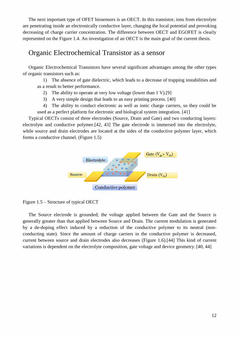
The next important type of OFET biosensors is an OECT. In this transistor, ions from electrolyte
are penetrating inside an electronically conductive layer, changing the local potential and provoking
decreasing of charge carrier concentration. The difference between OECT and EGOFET is clearly
represented on the Figure 1.4. An investigation of an OECT is the main goal of the current thesis.
Organic Electrochemical Transistor as a sensor
Organic Electrochemical Transistors have several significant advantages among the other types
of organic transistors such as:
1) The absence of gate dielectric, which leads to a decrease of trapping instabilities and
as a result to better performance.
2) The ability to operate at very low voltage (lower than 1 V).[9]
3) A very simple design that leads to an easy printing process. [40]
4) The ability to conduct electronic as well as ionic charge carriers, so they could be
used as a perfect platform for electronic and biological system integration. [41]
Typical OECTs consist of three electrodes (Source, Drain and Gate) and two conducting layers:
electrolyte and conductive polymer.[42, 43] The gate electrode is immersed into the electrolyte,
while source and drain electrodes are located at the sides of the conductive polymer layer, which
forms a conductive channel. (Figure 1.5)
Figure 1.5 – Structure of typical OECT
The Source electrode is grounded; the voltage applied between the Gate and the Source is
generally greater than that applied between Source and Drain. The current modulation is generated
by a de-doping effect induced by a reduction of the conductive polymer to its neutral (non-
conducting state). Since the amount of charge carriers in the conductive polymer is decreased,
current between source and drain electrodes also decreases (Figure 1.6).[44] This kind of current
variations is dependent on the electrolyte composition, gate voltage and device geometry. [40, 44]

13
Figure 1.6 – Schematic representation of dedopind process in OECT
The main working principle of an OECT as a sensor is the charge transfer between analyte and
Gate electrode. In case of the charge transfer the potential of electrolyte changes and the value of
this change (Vanalyte) is described by the Nernst equation. Since the Gate stays at a constant voltage,
in case of potential drop change at gate/electrolyte interface potential drop at electrolyte/channel
interface also takes place. This kind of changes are dependent on analyte concentration, therefore
the drain current is influenced by analyte concentration. Main requirements of effective OECT
sensors are:
1) Gate electrode should be smaller than channel
2) The charge carrier mobility should be as high as possible
3) Capacitance per unit area of polymer should be high
4) Ion to polymer penetration possibility should be high
5) Channel width should be high and length should be low
In case of satisfying such requirements the OECT would be sensitive enough to be used as an
electrochemical sensor. [45]
An OECT could also be successfully used as ion-to-electron converter. In this case transient
ionic current in electrolyte is induced by application of a positive gate voltage. Conducting polymer
film is reduced and cations are penetrating from electrolyte, therefor the drain current is decreasing.
So an OECT works as a converter of transient electronic current to the change of drain electronic
current.
The main characteristics of effective OECT ion-to electron converter are:
1) Gate electrode should be much larger then channel
2) Gate electrode should be non-polarizable
3) Polymer should be highly conductive
4) Channel width and thickness should be high
5) Channel length should be low
In case of following this structural rules the response of OECT ion-to electron converter is high.
As a result Organic Electrochemical Transistor is a normally on-transistor, in which the channel
is initially conductive, that represents a very efficient device to be used as an ion-to-electron
converter or a sensor that could successfully detect different types of analytes in different types of
media. It has a simple three electrode structure coupled with ionically and electronically conductive
layers that could be fabricated in a micro scale and operates under very low voltages. Thus OECT is
a perfect device to be used not only in-vitro, but also in-vivo to detect chemical or electric field
change in a media.

14
Motivation and thesis overview
Several analytical models have been recently developed to describe the operation principle of
OECT, predict the device response and analyze experimental observations of the device. [45-47]
However these models do not present an equal degree of precision in case of different OECT
geometries and applied potential. To fully understand the working mechanism of OECTs and
predict the device behavior it is absolutely necessary to establish more precise models.
In every good model consider the combination of three processes:
1) Movement of ions in, out and inside polymer layer (electrochemical process)
2) Recombination of the electronic and ionic charge carriers in the polymer
3) Transport of the charge carriers (holes) inside polymer
This is why the goal of this thesis is to develop a model which will describe precisely the
processes that happened inside Organic Electrochemical transistor after application of source-drain
and source-gate potentials. This thesis is dedicated to development of two models: simple analytical
model that suits well for parameters extraction and description of an OECT; numerical model that
allows describing the processes that occur inside OECT and especially inside a conductive polymer
layer, special attention is paid to dedoping process.
Chapter 1 Introduction is outlines the history and the field of Organic Electronics and
especially Organic Sensing Devices, among which the role of Organic Electrochemical Transistor is
important. In this chapter the outline and motivation of the thesis is also highlighted.
Chapter 2 Background information begins by investigating the question of conductivity of
ionically conductive layer, processes of ions interaction with the media and electrode surface. The
next part of this chapter gives an explanation of the nature of conductivity and transport properties
of organic conductive materials. The last part of this chapter describes current state of the art of
Organic Electrochemical Transistors including description of already existing models.
Chapter 3 Numerical model of an OECT describes several numerical models made in
COMSOL Multiphysics program, how these models are explaining the de-doping effect upon gate
voltage application, how they fit to experimental results and how they could be used to describe and
improve already existing devices. The link between the numerical and analytical models is also
established in this chapter.
Chapter 4 Analytical model of an OECT is dedicated to the analytical modeling explanation
and results, and importance of the information that could be extracted from the models.
Chapter 5 OECT device full model shows how all the models could be implemented
practically for any single device characterization and description.
Chapter 6 Experimental validation describes the experimental work that has been done on
Organic Electrochemical Transistors fabrication. The second part of this chapter is dedicated to the
fabrication of the device to prove the validity of the numerical model and to the results of the
Moving front experiment and local potential measurements.

15
CHAPTER 2. BACKGROUND INFORMATION
Any Organic Electrochemical Transistor consists of three electrodes [47]: Source, Drain and
Gate; a conductive polymer, which is placed between Source and Drain electrodes; an ionically
conductive material, which is located in contact with the conductive polymer and the Gate
electrode. To understand the working principle of this transistor as a whole, it is important to
describe the source of conductivity in each active part of the device and an origin of dedoping
process occurs inside the device. In this chapter an explanation of the nature of an electronic
conductivity of conductive polymer layer and an ionic conductivity of ionically conductive layer
will be given. An explanation of the de-doping process which is in charge of current modulation
will take place within the Chapters 3. and 4.
Ionically conductive materials
First important conductive layer in an Organic Electrochemical Transistor is an ionically
conductive layer. Different types of ionically conductive materials are used in OECT: ionic
liquids[48], ionogels[49], electrolyte solutions[9, 45, 47] and biological analytes[41]. The letter type
of an organic conductor is the widely used because it allows OECTs implementation as a biosensor
for different type of sensing applications, for example in-vitro for cell grows detection[50, 51] or in
vivo for brain activity recording[52]. Never the less the most used and studied ionically conductive
layer of an OECT is an electrolyte layer. This is why it is very important to give a brief description
of physics and chemistry of electrolyte solution.
Ion-Solvent interactions in electrolyte solution
Electrolyte is an electrically neutral solution of positive ions (cations) and negative ions (anions)
in a polar solvent, such as water. According to ion-solvent interaction electrolytes could be divided
on true and potential electrolytes. True electrolyte is ionically conductive in a pure liquid form (all
salts, such as NaCl, KCl are belonging to this type). Potential electrolyte (or ionogels) is non-
ionically conductive in its liquid form, but in contact with solvent chemical reaction takes place and
ions are produced, so electrolyte solution becomes ionically conductive. Examples of this type of
electrolyte are acetic acid and oxalic acid. So in ionically conductive solution not only weak
interactions are possible but also ion-forming chemical reactions.
Common electrolyte solutions that are used in Organic Electrochemical Transistors are solutions
of true electrolytes, such as NaCl and KCl in water. When salt is placed in water dissociation takes
place and two ions are formed:
NaCl(s) → Na(aq)+ + Cl−(aq)
(2.1)
Where (s) is a solid form of NaCl and (aq) indicates hydrated ions of Na+ and Cl
-.
Due to collisions of solvent and crystal walls, ions in lattice are going into the water phase
obtaining more energetically favorable state. This ion-solvent interaction causes formation of
conducting ionic solution (Figure 2.1a).[53]
Water in its liquid form has a dipole structure; its molecule contains two hydrogens bonded with
oxygen. Hydrogens have slightly positive charge and oxygen slightly negative. This makes water to

16
be a polar solvent and allows it to form hydrogen bonds (H-bonds) with nearby water molecules and
ions. Spherically symmetric electric field of ion tears water dipoles, which becoming trapped and
oriented near the ion (Figure 2.1b). These water molecules are immobilized near the ion, so they are
moving with the ion.
a.
b.
Figure 2.1 – Solvation process in aqueous electrolyte solution: a) Water molecule interaction
with NaCl salt crystal; b) Formation ion of surrounding hydration shells [54]
The closest layer of completely orientated water molecules near the ion forms an inner hydration
shell. The next layer of water molecule is still experience an influence of ion electric field, but
simultaneously it has ah influence of bulk water network, which also tries to orientate water dipoles.
So this in-between partially-orientated water adopts a compromise structure and form outer
hydrated shell. Hence in each ionic solution there is an interaction between solvent and ion due to
single ion electric field.
Ion-Ion interactions in electrolyte solution
It is important to mention that ion-solvent interactions are not the only ones that take place in the
solution. The other key process is an interaction between ions itself in the solution. Due to its
electric field an ion sees not only water dipoles, but also the other charged particles, such as the
other ions. These interactions are particularly important, because they affect equilibrium properties
of the solution. The degree of interactions depends on ionic charges and density in electrolyte, so on
its nature and concentration.
True electrolytes when placed in water are totally dissociated in ions; to fully understand
properties of true electrolyte solution it is necessary to fully understand ion-ion interactions. Ion-ion
interactions are assumed to have an electrostatic origin. The theory proposed by Peter Debye and
Erich Hückel lead to formulation of simplified, but never the less powerful model, of ion-ion
interaction and time-averaged ions spatial distribution in electrolyte solution.[55] To understand the
whole system it is important to look firstly on reference (central) ion with discrete charge selected
electrolytic solution consisted of solvated ions and water. Water molecules around this ion are
orientating and behaving as dielectric medium with dielectric constant equal to bulk water dielectric
constant (ε=80.1 at 293 K). The other ions around are treated in the medium in a form of an excess

17
charge density ρ (Figure 2.2). Central ion has an effect on this medium and excess of charge density
ρ varies with the distance from reference ion. In the same time net charge density is equal to 0, so
globally electrolyte is electroneutral.
Figure 2.2 – Graphic representation of Debye–Hückel model[56]
Reference ion attracts the neighborhood ions of an opposite sign so near the ion ρ≠0, this
attraction takes place due to electrostatic attraction forces between oppositely charged ions.
Together with electrostatic forces there are thermal forces that are knocking ions around and affect
on smoothening charge density to ρ=0 everywhere. So balance of these two forces leads local
excess for negative charge near the positive ion and positive charge near negative ion, with
simultaneous keeping global electrolyte electroneutrality.
Relation between excess charge density ρ and local potential φ are described by the Poisson’s
equation:
∇2𝜑 = −𝜌
𝜀𝜀0
(2.2)
where ∇2 - Laplacian operator considered to be:
∇2=
∂ 2
𝜕𝑥2+
∂ 2
𝜕𝑦2+
∂ 2
𝜕𝑧2
(2.3)
Freedom of ionic movement and charge distribution could be described by the Boltzmann
statistics:
𝑐𝑖 = 𝑐𝑖
0𝑒−𝑧𝑖𝑈𝑘𝐵𝑇
(2.4)
Where T is the temperature, kB - Boltzmann constant, zi is the charge of an ion and ci is a local
concentration of ion type (i=1, 2…), U- change in a potential energy of i particles when their
concentration is changed from bulk ci0 to local ci in the volume element dV. In case of no ion-ion
interaction local ci equals to bulk ci0, so U=0, in case of repulsion for two ions with the same sign ci
< ci0
, so potential energy is positive. In case of two oppositely charge ions, attraction takes place,
so the ci > ci0, which gives negative U.[57] U could be represented as Upositive =ziφq in case of

18
positive ion and Unegative=- ziφq for negatively charged ion, where q is the charge of an electron
and φ is the potential. Using the Boltzmann statistics for of monovalent ion one obtains
equations for positive and negative ions concentrations[56]:
𝑐+ = 𝑐𝑖0𝑒
qφ𝑘𝐵𝑇
(2.5)
𝑐− = 𝑐𝑖
0𝑒−𝑞φ𝑘𝐵𝑇
(2.6)
In the presence of several ions charge density would be:
𝜌 = 𝐹 ∑𝑧𝑖𝑐𝑖
𝑖
𝑞
(2.7)
Where F is a Faraday constant. Taking in account Boltzmann statistics:
𝜌 = 𝐹 ∑𝑧𝑖𝑞𝑐𝑖
0𝑒−𝑧𝑖qφ𝑘𝐵𝑇
𝑖
(2.8)
Poisson-Boltzmann equation is obtained by bringing together Boltzmann statistics with Poisson
equation:
∇2𝜑 = −
𝐹
𝜀𝜀0∑𝑧𝑖𝑞𝑐𝑖
0𝑒−𝑧𝑖qφ𝑘𝐵𝑇
𝑖
(2.9)
This equation could be linearized and solved analytically for diluted solution of an electrolyte
with the valence of ions zi=1 or zi=2. The result of the linearization has a Helmholtz equation
form[58]:
∇2𝜑𝑖(𝑟) = 𝐾2𝜑𝑖(𝑟)
(2.10)
Where r is the distance from the reference charge and K is the Debye screening length denoted
as:
𝐾2 =
2𝑞2
𝑘𝐵𝑇𝜀𝜀0∑𝑐𝑖
𝑖
𝑧𝑖2
(2.11)
This linearized analytic solution is represented at the Figure 2.3.

19
Figure 2.3 – Analytic solution of linearized Poisson-Boltzmann equation. Electric potential
dependence from the distance from atom[53]
It is not possible to solve the Poisson-Boltzmann equation analytically for electrolytes with high
concentrations of higher valence of ions, the only possible way to obtain the solution is a numerical
modelling.
Ionic transport in a solution
In a solution ions are moving under different applied forces to compensate their influence. This
movement has two aspects: an individual aspect and a group aspect. The individual aspect takes in
account an individual motion of every ion present in the solution; this ions movement is usually
random in direction and speed. The group aspect is more significant because it account on the group
ions movement in a certain direction producing the flux (or drift) of ions, this results not only
directed transport of charges, but also transport of mass.
Ionic flux could have three different origins:
1) The difference in the concentration in different regions of electrolyte would result a
concentration gradient, which produces a flow of ions to compensate the concentration
difference. This type of flux is called diffusion (Figure 2.4a).
2) The difference in electrostatic potentials in different electrolyte regions would lead to flow
of electric charges under the applied electric field - drift of charges (Figure 2.4b).
3) The gradient of temperature or pressure that gives rise to a flow of charges is called
convection.
Despite of the origin, any flux is a result of the reaction of a system, that is distorted, that leads
to an equilibrium maintaining.

20
a.
b.
Figure 2.4 – Origins of ionic flux in electrolyte: a) Diffusion due to gradient of concentration;
b) Migration due to gradient of potential
Diffusion is a movement of molecules to the region of lower concentration from the region of
higher concentration. The diffusion in the steady state is proportional to the gradient of
concentration. The diffusive flux relation with concentration is described by Fick’s law (here it is
presented in one spatial dimension):
𝐽𝑑𝑖𝑓 = −𝐷
𝑑𝑐𝑖
𝑑𝑥
(2.12)
Where D is the diffusion coefficient.
The diffusion coefficient or diffusivity could be calculated using the Einstein–Smoluchowski
relation[59]:
𝐷 =
𝜇𝑖𝑘𝐵𝑇
𝑞
(2.13)
Where µi - the electrical mobility of charged particle; q - electrical charge of the particle
As soon as equilibrium is reached and there is no more gradient of concentration only process of
self-diffusion, which originates from the random molecular motion, takes place in the solution. So-
called dynamic equilibrium is established. The diffusion process and an absence of the other
external forces will cause a complete and uniform mixing in the solution.
Under applied potential and created electric field ions are starting to compensate an electric field
to restore equilibrium of the system. So negatively charged ions are starting to drift towards the
higher potential (or more positive electrode immersed into solution); positively charged ions are
moving towards an area with lowest potential (or negatively charged electrode). As a result the
spatial separation of charges is produced, but electroneutrality of electrolyte is never the less
preserved. The drift flux of ions could be described with the following formula (here in one spatial
dimension):
𝐽𝑑𝑟𝑖𝑓𝑡 = −𝜇𝑖𝑧𝑖𝑞𝑐𝑖
𝑑𝜑
𝑑𝑥
(2.14)

21
Since the drift of ions takes place due to the fact that they are charged, the flux of negative and
positive ions could be separately presented as:
𝐽+𝑑𝑟𝑖𝑓𝑡 = −𝜇𝑖
+𝑧𝑖+𝑐𝑖
+𝑞𝑑𝜑
𝑑𝑥
(2.15)
𝐽−𝑑𝑟𝑖𝑓𝑡 = 𝜇𝑗
−𝑧𝑗−𝑐𝑗
−𝑞𝑑𝜑
𝑑𝑥
(2.16)
The convective term is used to describe excitant gradient temperature or pressure in the solution.
Combined together with the drift and diffusion terms the total ionic flux in electrolyte solution
could be described. So the Nernst-Planck equation is obtained. Here this equation is represented in
one-dimensional mass transfer form:
(2.17)
In general, in three-dimensions, the Nernst-Plank equation takes the following form:
𝐽𝑖 = −𝐷𝑖∇𝑐𝑖 −
𝑧𝑖𝐹𝑞
𝑅𝑇𝐷𝑖𝑐𝑖∇𝜑 + 𝑐𝑖𝒗
(2.18)
In case of an unstirred or stagnant solution with no gradients of density last, convective term is
suppressed:
𝐽𝑖 = −𝐷𝑖∇𝑐𝑖 −
𝑧𝑖𝐹𝑞
𝑅𝑇𝐷𝑖𝑐𝑖∇𝜑
(2.19)
In case of charged species, such as ions in electrolyte flux Ji, is equivalent to the current density.
This is how an ionic current in electrolyte is established.[60]
Ion-Electrode interaction in electrolyte solution
In an Organic Electrochemical Transistor the Gate electrode is put in contact, or immersed into
an ionically conductive solution. Understanding of the processes that takes place at this interface is
essential for understanding of the whole transistor working principle [13, 47, 61].
Electrode kinetics depends on electrode surface structure, purity and chemical reactions occur
there. It is possible to classify all electrodes according to chemical process that happen in their
interface in polarizable and non-polarizable electrodes[56].
Ideally polarizable electrode is characterized by absence of net reaction on its surface. That
means that only transient (displacement) current could flow through its interface due to non-
faradaic process. When potential is applied, charges will move towards an interface and accumulate
there. Charging (displacement) current will flow to compensate for an excess (or deficiency) of the
electrons in the interfacial electrode layer. Amount of this current will depend on the resistance in

22
the circuit. Basically, if there is no electrochemical reaction at the electrode it is possible to consider
the electrode-solution interface as analogous to a capacitor, which capacitance C is proportional to
stored charge q per applied potential E:
𝐶 =
𝑞
𝐸
(2.20)
The amount of charge at the metal electrode is equal to amount of charge in the solution. All the
stored charges form electrical double layer which composed of different sub-layers:
1) Inner layer (Helmholtz layer or Stern layer) where stay molecules which are specifically
absorbed (inner Helmholtz layer) and nearest approached solvated ions (outer Helmholtz
layer) that are non-specifically absorbed due to electrostatic interaction with an electrode.
2) Outer layer (Diffuse layer) is composed of the rest of redistributed non-specifically adsorbed
ions. It is located between the Outer Helmholtz Plane and the bulk of electrolyte. Thickness
of a diffuse layer is dependent on electrolyte concentration, for the small concentration it is
about 100 Ǻ.
Figure 2.5 – The schematic representation of an electrolyte structure near an ideally polarizable
electrode[62]
The presence of a diffuse double layer leads to the drop of potential near the electrode surface, so
existence of a double layer mustn’t be neglected for an accurate description of processes in any
electrochemical system.
An ideally non-polarizable electrode shows exactly the opposite type of behavior. Current is
passing freely through a perfectly non-polarizable electrode, so this electrode is characterized by an
interfacial reaction due to the presence of a faradaic process. If there is a more negative potential
applied on the electrode, electrons are gaining higher energy that could be sufficient enough for an
electron transfer from an electrode to ionic species adsorbed on the electrode. That means a
reduction reaction takes place on the surface and reduction current flows through the electrode-
electrolyte interface. An opposite - oxidation process could take place if an electrode potential is
high enough, so for electrons of ionic species there is more favorable to flow from an electrolyte to
an electrode, creating oxidation current. A critical potential at which these processes take place is
related to the standard electrochemical potential E0[56]. The current is proportional to stoichiometric
coefficients of the reaction at the electrode surface, so the amount of product made as a result of this

23
process is proportional to amount of charge that passes through the electrode’s interface. The
relationship between current (or charge that passes) and amount of product formed as a result of an
electrochemical reaction could be calculated by using the Faraday’s law:
𝑚 =
𝑄𝑀
𝐹𝑧
(2.21)
Where m - mass of the product as a result of an electrode reaction; M - molar mass of the
product; Q - electric charge passes the boundary; F - Faraday constant
Even though the potential of an electrode is not enough to perform an electrochemical reaction
other processes will, never the less, occur independently from the faradaic process at the interface.
The processes called non-faradaic, such as an adsorption and desorption would influence on a
solution-electrode interface. When potential is applied ions are migrating from the bulk to electrode
surface region, where the chemical reactions could take place, then they are adsorbed on the
electrode surface, where an electrochemical reaction with an electron transfer happens. External
current could flow due to the adsorption - desorption process, even if there is no electrochemical
reaction in the interface. Product desorbed after an electron transfer diffuses from an electrode
surface to the bulk of the electrolyte under the gradient of concentration and the gradient of an
electric field (in case if the product is charged). There are also possibilities of chemical reactions
between the product and the other species in the electrolyte in the bulk or in the near-electrode
region. (Figure 2.6)
Figure 2.6 – Schematic representation of the process near the non-polarizable electrode under
applied potential[56]
As a result when there is a reaction at the electrode: both faradaic and non-faradaic processes
take place; only non-faradaic process is possible in case of an absence of the reaction, but the
transient current could still flow due to adsorption-desorption process. Charging current could be
very significant in case of low concentration of an electrolyte. In some cases it could be even larger
than faradaic current. To conclude: both faradaic and non-faradaic processes must be taking in
account for the proper explanation of the reaction and charge transfer in a system.
Organic electronically conductive materials
Even though organic conductive materials in general have lower conductivity than inorganic
semiconductors or conductors they have a lot of advantages in comparison with inorganic materials,

24
such as: low cost, easy properties tuning by chemical modification and a lot of fabrication
possibilities by different techniques. Conductivity of organic conductors highly varies in the range
10-2
- 105
ohm-1
cm-1
, and depends on the type of organic conductor itself and also on its dopant.[63]
Organic conductors could be categorized into conductive small molecules and conductive polymers.
Small molecules are conductive materials that have the weight less than 1000 daltons, par contrary
conductive polymers are defined by mass bigger than 1000 daltons. According to IUPAC definition
polymer is a substance composed of macromolecules. Macromolecule is a molecule of high relative
molecular mass, the structure of which essentially comprises the multiple repetitions of units
derived, actually or conceptually, from molecules of low relative molecular mass.[64] In general
small molecules are more soluble in organic solvents, but polymers have better mechanical
properties and in general higher conductivity due to doping possibility.
Structure and conductivity of organic conductors
Even though the structure of conductive polymers and conductive small molecules is different,
the source of conductivity has the same chemical and physical nature. To understand the nature of
organic material conductance it is necessary to look precisely at the chemical structure and bonds’
configuration of these molecules.
The core element of an organic conductive material is carbon which has a 1s22s
22p
2 electron
configuration. Core orbital electrons are not participating in a chemical bonding, so in covalent
bond formation only four electrons from 2s22p
2 take part. While bonding with other atoms
depending on the number of combined orbitals, formation of orbitals with different type of
hybridization: sp1, sp
2, sp
3 is also possible. (Figure 2.7) As a result single, double or triple bonds are
formed.
methane CH4 ethylene (ethane) C2H4 acetylene (ethyne) C2H2
Figure 2.7 – Different types of carbon bond hybridizations and example of organic molecules
with this hybridization type[65]
Conducting properties of a polymer is closely related to its chains and bonds configurations. To
be conductive, organic material should have a chain with sp22pz hybridization. In conductive
materials one 2s orbital pairs with two 2p orbitals of a carbon atom to form 3 sp2 orbitals. Two out
of three sp2 orbitals form covalent bonds with neighboring carbon atoms and the last sp
2 orbital
forms a covalent bond with the side group, or with a hydrogen atom. This type of bond is the

25
strongest type of a covalent bond which is formed by head-on overlapping of the atomic orbital
(Figure 2.8), it is called σ-bond.[66, 67] The left pz orbital of a carbon atom overlaps with pz orbital
of a neighbored carbon atom and forms π bond. This type of bond is weaker than σ-bond, so it has
much less energy and less stability due to smaller overlap between two pz orbitals.
a. b.
Figure 2.8 – Formation of σ and π bonds in: a) ethylene molecule; b) benzene molecule
Bonding weakly, the electrons of a π bond are easily delocalized. Split of π bond on π bonding
and π* anti-bonding band leads to the energy-gap (Eg) formation. Conjugated molecules are the
molecules that have single and double bonds alternation. The increase of the number of double
bonds in a conjugated molecule leads to an energy-gap decrease. In case of large number of
interacting pz orbitals – fully occupied π-valence bond and empty π*-valence bond are formed. In
this case energy gap is determined as the difference between lowest unoccupied molecular orbital
(in conduction band)-LUMO and highest occupied molecular orbital (in valence band) - HOMO
(Figure 2.9).[68]
Figure 2.9 – Energy band formation in conjugated polymer materials[69]
The Band gap determines conductive properties of the material; it depends on molecule structure
and the number of repeating units, so this property could be tuned on molecular level by changing
the molecular structure of a material.
Conductive properties of organic materials are in a lot of cases highly dependent on additives
that could tune conductive properties towards much higher or lower values.

26
Doping of conductive materials
The most widely used class of organic conducting materials is conductive polymers. Piscine π-
conjugated polymers don’t have very high conductivity; this characteristic could be increased
trough the doping process. There exist n-type and p-type dopants. The conductivity of a material is
proportional to a doping concentration up to some extent, but even a small amount of dopant
(several ppm) could increase sufficiently the conductivity of a conjugated polymer. Dopant is
charge-transfer agent used to generate, by oxidation or reduction, positive or negative charges in an
intrinsically conducting polymer[4]. In conductive polymers dopant molecules are placed between
conjugated polymeric chains, it doesn’t form with them covalent bonds, but attached to them by
Coulomb force (Figure 2.10) [70]. Addition of a dopant forms an ionic complex with a conjugated
polymer by an electron exchange and provokes a charge separation near the polymer molecule
keeping, never the less, the global electroneutrality.
Figure 2.10 – Process of n-type doping of polymer molecule[71]
Chains of the conjugated polymer are starting to deform immediately after doping. The charge is
delocalized along several units of the polymeric chain, the difference between single and double
bonds decreases gradually, it causes a polaron creation. There are two types of polarons: P+ (hole)
polaron - electron from lower polaron level leaves and going to an accepter; P- (electron) polaron-
electron is leaving donor and goes to the accepter higher level. In terms of chemistry polaron is
lattice distortion associated radical ion.[72] Formation of polaron and bi-polarons (lattice distortion
associated union of two like charges) is possible in doped conjugated polymers. Polarons are
formed in case of low doping level and bi-polarons are formed in case of higher doping level.
Charge transport in conductive polymers is a multi-scale process. In an intra-molecular level
under applied potential bi-polaron or polaron travels along the chain causing charge propagation
with continuous polymer conformational changes[63]. Electron or hole current could be defined
depends on polaron origin. Charge hopping process occurs between two macromolecular chains in
the inter-molecular level. In supra-molecular level charge travels by a percolation between
amorphous and crystalline domains (Figure 2.11).

27
Figure 2.11 – Schematic representation of multi-scale transport in conductive polymers[73]
All three scales of charge transport are affecting the total charge transport process, so parameters
such as molecular chain flexibility and structure, packaging and aggregation should be considered
during synthesis and processing of the material[73].
Charge carrier transport in conductive polymers
Conductive polymers could be doped by one of two different types of dopant: n or p-type. As a
result depending on dopant type one of two polarons is created: p+- polaron and n
-- type polaron. So
the main charge carriers in conductive polymers are electrons and holes. The set of equations
governing electrons and holes transport in conductive polymers is very similar to those one that is
used for positive and negative ions transport description in electrolyte. So holes and electrons
density distribution and movement is described by the set of Drift-Diffusion and Poisson-
Boltzmann equations:
∇ ∙ 𝜀∇𝜑 = −𝑒(𝑝 − 𝑛)
(2.22)
𝑱𝑝 = 𝑒𝜇𝑝𝑝𝑬 + 𝑞𝐷𝑝∇𝑝
(2.23)
𝑱𝑛 = 𝑒𝜇𝑛𝑛𝑬 + 𝑞𝐷𝑛∇𝑛
(2.24)
Where p and n – holes’ and electrons’ concentrations, µp and µn - holes’ and electrons’ mobility,
Dp and Dn - holes’ and electrons’ diffusion constant.
Similar to an ionic case, this set of equations has an analytical solution only in limited amount of
very particular cases, so the proper solution could be obtained only in case of a numerical model
building.
PEDOT:PSS as an electronic conductor
The main interest of this thesis is an Organic Electrochemical Transistor, in particular OECT
with poly(3,4-ethylenedioxythiophene) polystyrene sulfonate (PEDOT:PSS) as electron-conductive
layer. PEDOT:PSS has a good biocompatibility, thermal, electrical and electrochemical
stability.[74] A relatively high conductivity, about 1000 S·cm-1
allows to fabricate not only
conductive channel, but also Source, Drain and Gate electrodes from PEDOT:PSS[75].
From a chemical structure point of view, PEDOT:PSS is a mixture of polytheophene polymer
(PEDOT) doped by polystyrene sulfonate (PSS) polyanion (Figure 2.12). PEDOT:PSS is a heavily

28
doped p-type conductive polymer, in which PSS- compensates a positive charge from PEDOT
backbone that creates a positive polaron redistributed through several polymeric units and forms a
poly-ion complex[76].
Figure 2.12 – Chemical structure of PEDOT :PSS p-type conductive polymer (modified
from[77])
PEDOT:PSS complex exists in water in a form of colloidal gel particle, which could be
processed into a fiber, thin or thick film by the variety of techniques, such as spin-coating, inkjet
printing, flexography, lithography[76].
PEDOT:PSS is usually synthesized from EDOT monomer and PSS in water phase with an
oxidizing agent – sodium peroxodisulfate. PEDOT itself is not soluble in any solvent, but PEDOT
in oligomeric form (about 20 units) in ionic complex with PSS is dispersed in an aqueous medium.
The ratio of PEDOT:PSS which is normally used for organic electrochemical transistors fabrication
is 1:2.5 with amount of water equal to 2%. A dispersion contains 1-2.5% PEDOT:PSS in water has
an optimal viscosity to be used by main deposition techniques[76]. Different dispersions of
PEDOT:PSS are commercially available by Clevios and Sigma Aldrich. To better crosslink
PEDOT:PSS film, for more stable operation in an aqueous environment, (3-glycidyloxypropyl)
trimethoxysilane (GOPS) is often added[78]. It is possible to enhance the conductivity of a
PEDOT:PSS layer by different additives integration during film formation. For example, ethylene
glycol (EG) addition increases both an inter- and intraparticle charge carrier transport.[79] The
addition of 3% EG would lead to an increase of PEDOT:PSS conductivity up to two orders of
magnitude (from 3 S cm-1
to 175 S cm-1
), but further increase of ethylene glycol concentration
would lead to conductivity decrease. The possible explanation of this effect could be that in a
pristine film PEDOT:PSS has the structure of aggregates of an amorphous PEDOT surrounded by
an insulating PSS (Figure 2.12d) where the transport is unfavorable due to relatively high activation

29
energy (about 20 meV). An addition of a small amount of EG would promote the PEDOT phase
crystallization and the insulating PSS shell thickness decrease, which lowers an activation barrier to
5.1 meV and promotes a charge-carrier hopping. Further increase of EG concentration would lead
to increase of conductive domains size and defects formation[77]. Further enhancement of
conductivity is also possible by different methods, for example by a solvent addition[80, 81] or a
thermal treatment [82].
One of important and remarkable properties of PEDOT:PSS is it’s electrochromic behavior.
Electrochromism is a property of a material to reversibly change the color as a result of changing
the state due to redox reaction[83]. In case of PEDOT:PSS the color is switching from light-violet
(near-infrared) to deep blue (visible). Figure 2.13 represents an absorption spectrum of
PEDOT:PSS. It could be seen that upon application of the potential the absorption spectrum has
been shifted towards lower waive-length.
Figure 2.13 – Absorption spectrum of PEDOT:PSS in OECT at 0V and 1V of applied Gate
potential[84]
This kind of behavior could be explained as a result of following redox reaction[85]:
𝑃𝐸𝐷𝑂𝑇+ + 𝑒− ↔ 𝑃𝐸𝐷𝑂𝑇0
(2.25)
The potential difference change of the system leads to a change of the system’s free energy. Thus
this potential change is linked with all sorts of electrochemical change, such as electrochemical
reactions that take place in the system.
If the reversible redox reaction takes place in the system (such as it is PEDOT+↔ PEDOT
0), than
the Nernst equation is used to describe the dependence of the reagent-product concentration from
electrochemical potential[86]. It is worth mentioning that the Nernst equation is only used to treat a
thermodynamically and electrochemically reversible system in the equilibrium state, which means
when rates of a reduction reaction and an oxidation reaction are equal.
If the reaction in the system could be described by the following equation:
𝑂𝑥+ + 𝑒− ↔ 𝑅𝑒𝑑0
(2.26)
Where Ox+ is the concentration of oxidized (reagent) species; Red
0 – concentration of reduced
(product) species, then the concentration-potential dependence could be calculated from the
following Nernst equation of half-reaction:

30
𝐸 = 𝐸0 +𝑅𝑇
𝑛𝐹𝑙𝑛
𝑎𝑂𝑥
𝑎𝑅𝑒𝑑
(2.27)
Where αOx and αRed are activities of oxidized and reduced species.
For low concentrations it is possible to use the concentrations of reduced and oxidized species
instead of activities:
𝐸 = 𝐸0 +
𝑅𝑇
𝑛𝐹𝑙𝑛
𝐶𝑂𝑥
𝐶𝑅𝑒𝑑
(2.28)
Where COx and CRed are the concentrations of an oxidized and a reduced species; R - standard gas
constant; T - temperature; n - number of transferred electrons; E0-standard potential of the reaction.
Using this equation it is possible to calculate the concentration of a reagent:
𝐶𝑂𝑥 =
𝐶𝑅𝑒𝑑
𝑒𝑛𝐹(𝐸−𝐸0)
𝑅𝑇
(2.29)
𝐶𝑂𝑥 = 𝐶𝑅𝑒𝑑𝑒
𝑛𝐹(𝐸0−𝐸)𝑅𝑇
(2.30)
From this representation of the Nernst equation it could be easily seen that under equilibrium,
concentration of the reactant (COx) is proportional to concentration of the product and reversely
proportional to the temperature of the system and highly dependent on applied potential: if applied
potential is higher than standard potential of reaction, then equilibrium is shifted towards the higher
concentration of the product and vice-versa[56].
According to the Figures 2.14a and 2.14c, the reduction potential for PEDOT:PSS molecules
from three different producers is from 0V to -0.1V and oxidation potential is about 0.1-0.2 V[83].
As soon as the applied potential is greater than reduction potential of PEDOT+, the reduction
reaction takes place and PEDOT+ is transferred to PEDOT
0. The result of a redox reaction of the
real PEDOT:PSS is shown on Figure 2.14b.

31
a.
b.
c.
Figure 2.14 – Redox behavior of PEDOT:PSS: a) Theoretical cyclic voltammogram; b)
Electrochromic PEDOT:PSS behavior as a result of redox reaction[87] ;c) Cyclic voltammogram of
PEDOT:PSS [88]
An electrochromic behavior of PEDOT:PSS is interesting not only from its application point of
view. Being a wonderful tool to track ions, PEDOT+ distribution and device conductivity profile it
also helps to understand the dedoping process that happens upon the application of certain gate
potential in Organic Electrochemical Transistors.
OECT modeling
There are two different approaches to a device modeling: numerical and analytical. The purpose
of both types of models is a correct description and prediction of the main characteristics of a
modeled object and processes occurring inside modeled object under known applied conditions. An
analytical model normally allows calculating precisely the main characteristics of an investigated
object and obtaining the exact solution. A numerical modeling is used when parameters and all
device characteristics couldn’t be calculated analytically. Numerical models do not give an exact
solution of solved equations; instead, the solution with a certain degree of approximation is the
result of numerical calculations. Never the less, both types of models are important for
understanding the device physics and chemistry. To build up a working model it is useful to study
precisely the already excising state of the art.
There exist several analytical models of an OECT that could give, up to some extent, an
explanation and prediction of the device properties. Most of the models are considering depletion
mode of an OECT operation. Different behavior of Organic Electrochemical Transistors is well
defined for transient and steady-state. These models could be differentiated one from another taking
in account to which state of operation a model is dedicated. A lot of models are looking at an

32
OECT from a point of view of physical generalization, and represent this device as a sum of
resistive and capacitive elements.
The first model of OECT by Prigodin et al.[89] described the foundation of OECT modeling
from the point of solid state physics. In this model mechanism of the channel conductivity and
current decrease was attributed to holes mobility decrease due to cations injection under the applied
Gate potential. This model being purely theoretical doesn’t allow the data extraction and prediction.
The second model made by Robinson et al.[90] par contrary proposed to look at an OECT from
an electrochemical and electrostatic point of view and linked the drop in conductivity with the
applied potential induced by a de-doping process due to cations penetration with the following hole
extraction. This model is numerical and also doesn’t allow the straightforward data fitting and
parameters extraction.
The third model made by D.A. Bernards and G. G. Malliaras[47] look at OECT, operating in
non-Faradaic regimes, as at sum of two circuits an ionic and an electronic. They come across two
behaviors of an OECT in transient and steady-state. The ionic part (electrolyte) is modeled as a
resistor and a capacitor in series. (Figure 2.15) Electronic part (conductive polymer) is modeled
using Ohm’s law.
a.
b.
Figure 2.15 – Modeling of ionic part of OECT device as a resistor and capacitor in series: a)
Schematic representation of the device structure used in the model. Drain is located at x=L and
Source at x=0; b) Circuit-like representation of the device, where the charge Q(x) is coupled with
voltage according to the position x along the conductive channel
In the electronic part, the channel current density was calculated by the Ohm’s law in one
dimension with x being the position along the channel between source and drain:
𝐽(𝑥) = 𝑞𝜇𝑝(𝑥)
𝑑𝑉(𝑥)
𝑑𝑥
(2.31)
where, q- elementary charge, p(x) - hole density with respect to x, µ - hole mobility, V(x)
potential along the channel.
As a result of de-doping process, the amount of holes is decreasing; this could be described by
the following equation:
𝑝(𝑥) = 𝑝0 (1 −
𝑄(𝑥)
𝑞𝑝0𝑊𝐿𝑇)
(2.32)

33
Where p0 – initial doping level (holes density); Q(x)- total charge of cations injected from the
electrolyte as a result of de-doping process. Gradual channel approximation was used to define the
gradient of charge density. W, L, T are channel width, length and thickness accordingly.
Since the ionic part was defined by a capacitor and a resistor in series, then the amount of
charges injected to the layer could be calculated according to the following expression.
𝑄(𝑥) = 𝑐𝑑𝑊𝑑𝑥(𝑉𝑔 − 𝑉(𝑥))
(2.33)
Where cd is a differential capacitance and Vg is an applied gate potential.
Combining all three expressions above it is possible to calculate the current in the channel
depending on applied Gate potential.
𝐼(𝑥) = 𝑊𝑇𝑞𝜇𝑝0 [1 −
𝑉𝑔 − 𝑉(𝑥)
𝑉𝑝]𝑑𝑉(𝑥)
𝑑𝑥
(2.34)
Where Vp is a pinch-off potential - Gate potential at which total channel de-doping takes place in
the absence of applied drain potential.
As a result, using this model it was possible to calculate the current in OECT in case if a non-
faradaic process is taking place on ideally polarizable gate electrode with different applied gate
potentials, working in different regimes (partial de-doping, linear and saturation). Even though this
model is suitable for current-voltage profiles characterization and predictions it has several
drawbacks, such as inability to describe characteristic s-shape transfer curve and also not precise
enough fitting between experimental and modeled results.
Extension of the third model towards the description of the faradaic regime of an OECT
operation was made one year after by Bernards et al.[13] . This model takes in account an analyte
electrochemical reaction at the Gate electrode, it allows to link the drain current response to the
analyte concentration change in the process of enzymatic sensing of glucose.
Next model made by Yaghmazadeh et al [45] extends the two previous models to obtain the
better fitting of the experimental and modeled profiles. The improvement was concerning more
precise variation of the potential along the channel and the channel polarizability. But still, as the
analytical models mentioned above, it was not able to explain the saturation of the current and the
shape of the transfer curve.
It should be also mentioned the numerical model made by Stavrinidou et al.[46] which explains
an ionic movement inside the PEDOT:PSS layer, since this movement and the de-doping process
are the least explained and understood processes in Organic Electrochemical Transistors. The model
represented the moving front experiment[91] in the PEDOT:PSS layer (Figure 2.16). For this
experiment the device with two electrode structure, electrolyte and conductive polymer was
fabricated. Ions from the electrolyte are claimed to move inside the PEDOT:PSS conductive
polymer layer causing the de-doping effect and provoking holes extraction at the grounded
electrode (Source).

34
Figure 2.16 – Visualization of charge distribution in the polymer during Moving front
experiment: positive ions injected from electrolyte are replacing the holes in the polymer during the
Moving front propagation
It is stated that movement of this ionic front could be visualized by transient optical
measurement of the conductive polymer layer transmission. Local concentration of the PEDOT+
could be extracted from the measurements. Figure 2.17.1 represents experimentally measured
optical transmission light intensity, after application of Gate-Source potential, since ΔΤ is
proportional to electrolyte injected cations concentration, then this experimental measurements
could be compared with modeled by Stavrinidou et al. moving front (ions concentration) profile
(Figure 2.17.1).
1.
2.
Figure 2.17 – Moving front experiment: 1) Experimentally measured evolution of the de-doping
front for time t from 5 to 50 seconds (ΔΤ is the change of transmitted light intensity along the
conductive polymer channel); 2) Numerically modeled moving front for time t=2, 4, 6, 8, and 10
µs: a) Spatial distribution of injected electrolyte cations (gray dotted), anions holes (black dotted)
and positive charges due to electrolyte ions injection (solid black); b) Holes spatial density; c)
Potential profile
Even though the time and the channel length are not the same it is not difficult to notice that
modeled and experimental moving front profiles have the same shape and type due to ions injection.
Stavrinidou et al. model predicts successfully ions concentration in the PEDOT:PSS layer after
Gate-Source potential application it is not clear what would happen when the steady-state will be
reached, when the moving front will stop and why, how the final ionic distribution would look like.
For the full and clear description of OECT all of these questions need to be answered.

35
There are no doubts that already existing models could be used to describe OECT and quantify
changes in the current with change in applied potential, up to some extent. But each of them have
some drawbacks: generally, the existing analytical models are showing the good fit only to some
experimental data and only for limited applied potentials; numerical models based only on the
Poisson-Boltzmann and the Nernst-Planck equations are describing quite well only transient
behavior of OECT due to all assumptions made about an ionically initiating de-doping of
PEDOT:PSS. As a result, some effort needs to be made to build up mode precise numerical and
simple analytical models for the complete description of an OECT working principle.
Conclusion
The understanding of any system starts with the understanding of a working principle of each
part of this system. An Organic Electrochemical Transistor consists of two active layers. One of
them is ionically and the other is electronically conductive. And both of them together are making a
complicated and undividable system.
This Chapter was dedicated to the understanding of the origin of the conductivity in each of the
layers and key processes that occur inside of each of them. In an electronically conductive layer the
source of conductivity is an electron or a hole propagation under the gradient of applied potential or
gradient of concentration. In ionically conductive layer charge carriers are positively or negatively
charged ions, which are moving in the media due to drift, diffusion or convection. Even though the
types of charge carriers are different, forces causing their movement have the similar origin. There
are some other processes that need to be considered for a successful modeling: faradaic and non-
faradaic processes on the electrode immersed in electrolyte, including an electrochemical reaction
and a displacement current. Sum of all of these processes together with the de-doping process,
which mechanism is one of the focal points of current thesis, is the core subject of further
investigation and modeling.
It is not possible to proceed with the subject without mentioning, at least briefly the current state
of the art in particular area of the research interest. In this case the already excising analytical and
numerical models were the starting point for the following research.

36
CHAPTER 3. STEADY STATE NUMERICAL MODELING
Numerical modeling of Organic Electrochemical Transistor will allow building up the picture of
device operation and processes solving set of equations, such as Nernst-Planck together with
Poisson-Boltzmann, that couldn’t be solved otherwise.
For numerical modeling we used COMSOL Multiphysics®[92], software based on finite element
approach. This software is based on advanced numerical methods for physical-based simulation and
modeling. To solve the complex problem, the software divides the whole system in a set of small,
so called finite elements. Then set of equations is resolved within each of this element with
following reassemble into a bigger continuous system of equations that describes fully the modeled
object. So this software gave us a nice tool for the system understanding and description.
COMSOL Multiphysics®
allows to couple and model several types of processes happening
simultaneously in the same system. It is possible to model chemical reaction together with physics
linked with applied potential and transport of different types of charged species, such as electrons
holes and ions. For OECT modeling two modules of COMSOL Multiphysics® were coupled
together: Chemical Species Transport (Transport of Diluted Species) and AC/DC (Electrostatics)
from Electrochemical Module. Two types of numerical simulations were made: one dimensional
model with two electrodes and two dimensional device model with full structure (three electrodes).
This approach was aimed to deeper understanding of inner device physics such as de-doping
process and electrolyte influence and distribution in PEDOT:PSS conductive polymer layer.
Ions penetration under applied Gate potential assumed to be the main process responsible for
PEDOT:PSS layer de-doping and as a result electrical current dropping in the channel[13]. This
theory is the most widely accepted one [44, 47, 93]. According to this theory under applied
potential positive ions from electrolyte penetrate inside the PEDOT:PSS layer, then are trapped
near PSS- unit where they replace PEDOT
+, thus maintaining an electrical neutrality. As a result,
the amount of holes in the polymer layer decreases, and since in PEDOT:PSS the electrical current
is holes-generated, the current decrease is linearly proportional to the hole amount decrease (Figure
3.1a).
a.
b.
Figure 3.1 – Widely accepted representation of de-doping process[47]: a) Charges distribution
inside OECT before gate voltage application; b) De-doping process representation upon applied
gate potential

37
In this approach the fact that reduction of PEDOT+ takes place after application of certain redox
potential is not considered. So building up one dimensional model first, which takes into account
redox reaction in conductive polymer layer, ion movement and faradaic process on gate electrode
under different applied potentials, is mandatory.
One-dimensional modeling
Before building up full device model it is necessary to understand how the two main events:
electronic and ionic are interacting between each other and how ions from the electrolyte act on
PEDOT:PSS layer after penetration.
For this, a one dimensional model was developed first. Basically this model is aimed to model
ions penetration from electrolyte to the conductive polymer layer and the result of electrolyte-
conductive polymer interaction in steady state. Figure 3.2 represents modeled geometry.
Figure 3.2 – Schematic representation of COMSOL numerical 1D model geometry. At the right
hand side grounded source electrode is situated so V(W)= 0 V; at the left hand side there is a gate
electrode, so V(0)=Vgs; in between there are ionically conductive layer that contains Cl- and Na
+
ions and electronically conductive PEDOT:PSS layer, where Na+
are penetrating upon de-doping
occurred.
Modeled device consists of two layers:
1) Ionic layer with 100 mM of NaCl solution. Thickness of the layer is W-d=900 nm
2) Electronically conductive PEDOT:PSS layer. Initial density of PEDOT+ (mobile holes)
being equal to the density of PSS- (immobile electrons) is 10
18 cm
-3. Thickness of modeled
conductive polymer layer is d=100 nm. This thickness was chosen since real OECT
biosensors have thickness of the same order of magnitude.
According to the most popular theory applied potential between Gate and Source is pushing
positive Na+ ions inside conductive channel. But this theory does not take into account the redox
reaction of PEDOT+ under applied potential. The following model seems more realistic since it also
includes the electrochemical nature of the process:
1) Before Gate-Source application ions are redistributed in electrolyte, PEDOT:PSS channel
is fully doped (Figure 3.3a). In case of three electrode device the current is proportional to
applied Source-Drain potential
2) A potential applied between gate and source electrodes reduces the amount of holes by
polymer reduction according to the Nernst equation, leaving uncompensated negative PSS-
charge in PEDOT:PSS layer (Figure 3.3b). At the same time in case of polarizable
electrode (for example Ag/AgCl) the oxidation reaction takes place on the gate electrode,
amount of Cl- that is oxidized at the Gate electrode is equal to amount of PEDOT
+ reduced
in conductive polymer layer, thus global electroneutrality in the electrolyte is preserved.

38
3) To maintain electroneutrality in the polymer positive Na+ ions are intercalated in the
PEDOT:PSS layer so that the total amount of positive charge PEDOT+
left + Na+
intercalated is
equal to that of negative PSS- (Figure 3.3c). This process starts together with PEDOT
+
reduction. Since the amount of Na+ ions that entered the conductive polymer is equal to that
of PEDOT+ left which in turn is the same amount of Cl
- reacted at the Gate, the
electroneutrality in the whole system is preserved.
a.
b.
c.
Figure 3.3 – Simplified representation of moving front modeled at different stage: a) Before
Source-Gate potential is applied; b) Right after potential application part of PEDOT:PSS layer is
reduced, oxidation reaction occurs at Ag/AgCl electrode; c) Excess of neutral charge in the polymer
provokes positive Na+ to diffuse from electrolyte to restore the charge neutrality in polymer and
electrolyte layers
As it was mentioned before, to build up a realistic OECT model it is important to take in account
all major processes occurring inside the device under applied potential.
Electrolyte layer modeling
Our modeling of an OECT starts with that of the electrolyte layer and processes definition, since
processes in electrolyte with immersed electrode are well-described in the literature. In the model
NaCl solution was used as electrolyte. In aqueous environment hydrolysis takes place and two ions
are formed:

39
NaCl(s) → Na(aq)+ + Cl−(aq)
(3.1)
Where (aq) indicates hydrated ions of Na+ and Cl
+.
These ions motion in the electrolyte was modeled by Nernst-Planck equation for Na+
and Cl-
ions:
𝐽𝑁𝑎 = −𝐷𝑁𝑎∇𝑐𝑁𝑎 −
𝐹𝑞
𝑅𝑇𝐷𝑁𝑎𝑐𝑁𝑎∇𝜑
(3.2)
𝐽𝐶𝑙 = −𝐷𝐶𝑙∇𝑐𝐶𝑙 +
𝐹𝑞
𝑅𝑇𝐷𝐶𝑙𝑐𝐶𝑙∇𝜑
(3.3)
For the model we are assuming that there is no mechanical stirring or thermal non-equilibrium
that is why the last convective term of Nernst-Planck equation is equal to zero.
Local potential in any point of the device is calculated by Poisson-Boltzmann equation takes into
account all positive and negative charges concentration:
∇ ∙ 𝜀∇𝜑 = −𝑒(𝑐𝑁𝑎 − 𝑐𝐶𝑙 + 𝑐𝑃𝐸𝐷𝑂𝑇+ − 𝑐𝑃𝑆𝑆)
(3.4)
Where 𝑐𝑁𝑎, 𝑐𝐶𝑙, 𝑐𝑃𝐸𝐷𝑂𝑇+ , 𝑐𝑃𝑆𝑆 are the local concentrations of positive Na+
, negative Cl- ions,
PEDOT+ holes generating units and PSS
- units.
In the electrolyte layer global electroneutrality takes place and Poisson-Boltzmann equation for
this part of two-electrode device is:
∇ ∙ 𝜀∇𝜑 = −𝑒(𝑐𝑁𝑎 − 𝑐𝐶𝑙) (3.5)
To maintain system layer global neutrality, several global constraints were put in the system:
1) To preserve constant amount of Na+ in the system:
∫ 𝑐𝑁𝑎 𝑑𝑥
𝑊
0
= 𝑐0 ∙ 𝑊
(3.6)
Where c0 is initial Na+ concentration: 100 mM in the electrolyte layer and 0 mM in conductive
polymer layer.
2) To preserve global electroneutrality in the electrolyte layer it is necessary that the total
concentration of Cl- is equal to that of Na
+:
∫ 𝑐𝑁𝑎 𝑑𝑥
𝑊−𝑑
0
= ∫ 𝑐𝐶𝑙
𝑊−𝑑
0
𝑑𝑥
(3.7)
3) To preserve global electroneutrality in conductive polymer layer:

40
∫ 𝑐𝑁𝑎 𝑑𝑥
𝑊
𝑊−𝑑
= ∫ (𝑐0𝑝− 𝑐𝑃𝐸𝐷𝑂𝑇+)
𝑊
𝑊−𝑑
𝑑𝑥
(3.8)
where c0_p is initial PEDOT+ concentration (which is also the concentration of PSS
-).
The set of equation above is successfully describing all processes happen in electrolyte layer for
any Organic Electrochemical Transistor. This set of equations should be coupled with another set of
equations that is describing conductive polymer layer and a result of de-doping process.
Electronically conductive polymer layer modeling
Electrically conductive layer is made of PEDOT:PSS polymer which is electrically neutral due to
equal amount of PEDOT+
and PSS- units and equal to number of holes. Since PEDOT:PSS is a p-
type conductor, then the current in this polymer is a hole - current. Even though holes are moving
under applied electric field PEDOT+ and PSS
- units are immobile. Amount of holes is correlated
and almost equal to amount of PEDOT+ units, so in the equation below CPEDOT+ is the concentration
of hole generated PEDOT+ units, which is equal to hole concentration.
Knowing that number of PEDOT+
units is highly dependent from applied potential due to redox
reaction:
𝑃𝐸𝐷𝑂𝑇+ + 𝑒− ↔ 𝑃𝐸𝐷𝑂𝑇0
(3.9)
it is possible to calculate it according to Nernst equation for low concentrations:
𝜑 = 𝐸0 +
𝑅𝑇
𝐹𝑙𝑛
𝐶𝑃𝐸𝐷𝑂𝑇+
𝐶𝑃𝐸𝐷𝑂𝑇0
(3.10)
𝜑 = 𝐸0 +
𝑅𝑇
𝐹𝑙𝑛
𝐶𝑃𝐸𝐷𝑂𝑇+
𝐶0_𝑝 − 𝐶𝑃𝐸𝐷𝑂𝑇+
(3.11)
Hence:
𝐶𝑃𝐸𝐷𝑂𝑇+ =
𝐶0_𝑝
1 + 𝑒𝐹(𝐸0−𝜑)
𝑅𝑇
(3.12)
Normally the Gate electrode is taken as the reference electrode, but in OECT the Source plays
this role; it will lead to the Nernst equation modification:
𝐶𝑃𝐸𝐷𝑂𝑇+ =
𝐶0_𝑝
1 + 𝑒𝐹(𝜑−𝐸0)
𝑅𝑇
(3.13)

41
For proper use of the latter equation it is necessary to estimate E0, which is a redox potential of
net reaction. So if we are taking in account faradaic process of Cl- oxidation on Ag/AgCl the gate
electrode. Then net reaction is described by the following equation:
𝑃𝐸𝐷𝑂𝑇+ + 𝐶𝑙− + 𝐴𝑔0 ↔ 𝑃𝐸𝐷𝑂𝑇0 + 𝐴𝑔𝐶𝑙
(3.14)
Reaction at the gate electrode would be described by Butler-Volmer equation:
𝐽 = 𝑛𝐹𝑘𝐵 [𝐶𝐴𝑔𝐶𝑙𝑒
−(𝛼𝐹𝑅𝑇
)(𝐸0−𝐸) − 𝐶𝐶𝑙−𝑒((1−𝛼)𝐹
𝑅𝑇)(𝐸0−𝐸)
]
(3.15)
where: J - electrode current density, E - electrode potential, E0
- equilibrium potential, T -
absolute temperature, F - Faraday constant, R - universal gas constant, α - so-called cathodic charge
transfer coefficient
To simplify the model global constraint was used, concentration of Cl- in electrolyte was
assumed to be equal to Na+ concentration, so the result of the electrochemical reaction on the Gate
electrode was modeled, not the reaction itself.
But it is important to know redox potential of the Gate electrode reaction to calculate E0 – cell
redox potential:
𝐸0 = 𝐸𝑐𝑎𝑡ℎ𝑜𝑑𝑒0 − 𝐸𝑎𝑛𝑜𝑑𝑒
0
(3.16)
In case of Ag/AgCl in NaCl (100 mM) E0
anode is 0 V, for PEDOT+ reduction reaction E
0cathode is
V, so E0 is about -0.1 V.
Since PEDOT:PSS layer is conductive it is necessary to consider charge carrier movement:
𝐽𝑃𝐸𝐷𝑂𝑇+ = −𝐷𝑃𝐸𝐷𝑂𝑇+ ∙ ∇𝑐𝑃𝐸𝐷𝑂𝑇+ −
𝐹𝑞
𝑅𝑇𝐷𝑃𝐸𝐷𝑂𝑇+ ∙ 𝑐𝑃𝐸𝐷𝑂𝑇+ ∙ ∇𝜑
(3.17)
In any case, considering all processes happening in all the layers, global electrical neutrality
must be maintained. To understand PEDOT:PSS de-doping process it is necessary to consider that
after the reduction of PEDOT+ there are two possible types for Na
+ distribution in conductive
polymer layer:
1) According to a widely accepted picture, Na+
is locally electrostatically attached to PSS-, taking
exactly the place of PEDOT+ that was reduced. In this case local neutrality of de-doped
conductive polymer layer is preserved as well as global neutrality of the whole system. We call
this case the Local Neutrality numerical model.
2) It should be also taken in account that an electrostatic force between Na+ and PSS
- is small and
it could be not enough to stop Na+ from moving inside the conductive polymer layer, so the
ions could drift under applied potential towards the less positive Source electrode. We will call
this second possibility the Global Neutrality numerical model.
Both of these two models could have a rational physical explanation, to understand which one of
the models is the closest to the real situation in OECT comparison of the modeled profiles with
experimental data was made.

42
No ion penetration (EGOFET-like) model
Before developing any model including ion penetration from electrolyte and its movement inside
conductive polymer layer it is better to take a look at simple reference model. For Organic
Electrochemical Transistor this type of reference model could be Electrolyte Gated organic Field
Effect Transistor[93] (EGOFET) model.
EGOFET is a transistor that operates in accumulation mode; similarly to the OECT it consists of
two layers: one ionically conductive and one electronically conductive. The difference between
these two types of transistors is that in EGOFET ions do not penetrate from ionically conductive
layer into the electronically conductive medium; rather, they accumulate on its surface, creating an
electrical double layer. (Figure 3.4)
Figure 3.4 – Electrolyte Gated Field Effect Transistor structure[93]
In this type of transistor there is no charge transfer between ions and electronically conductive
material. Studying this model and comparing it with ion-penetrating case would allow to understand
deeper the effect of penetrated ions on conductive polymer properties.
One-dimensional structure was modelled, equal to what represented in Figure 3.4, with 900 nm
layer of NaCl as electrolyte and 100 nm layer of PEDOT:PSS as a conductive polymer. In this
model the concentration of the electrolyte was 100 mM, no reaction at the gate and no ion
penetration inside conductive polymer layer were assumed. Influence of ions on the conductivity of
conductive polymer layer was due to accumulation of the ions at the electrolyte-polymer interface.
Nevertheless the concentration of PEDOT:PSS is local potential-dependent according to the Nernst
equation (3.20) .
Poisson-Boltzmann equation for the electrolyte layer writes:
∇ ∙ 𝜀∇𝜑 = −𝑒(𝐶𝑁𝑎 − 𝐶𝐶𝑙)
(3.18)
And for the conductive polymer layer:
∇ ∙ 𝜀∇𝜑 = −𝑒(𝐶𝑃𝐸𝐷𝑂𝑇+ − 𝐶𝑃𝑆𝑆)
(3.19)
Concentration of PEDOT+ is calculated according to Nernst equation:

43
𝐶𝑃𝐸𝐷𝑂𝑇+ =
𝐶0_𝑝
1 + 𝑒𝐹(𝜑−𝐸0)
𝑅𝑇
(3.20)
Concentration of Na+ ions, as well as PSS
- is constant in the system, but to preserve the global
electroneutrality and account for the reaction on the gate electrode Cl- concentration is calculated
so, that:
∫ 𝐶𝐶𝑙𝑑𝑥
𝐿−𝑑
0
= 𝐶0_𝑒 ∙ (𝐿 − 𝑑) − ∫(𝐶0𝑝− 𝐶𝑃𝐸𝐷𝑂𝑇+)𝑑𝑥
𝐿
𝐿−𝑑
(3.21)
Combining equations (3.18-3.21) numerical calculations were performed. As a result potential
and concentration profiles along the device were calculated. In Figure 3.5 the potential profile along
device and along conductive polymer layer is represented. In Figure 3.5a small drop of the potential
could be identified near the Gate electrode due to existing double layer, then there is a flat
equipotential region inside electrolyte; and main drop of the potential occurs inside conductive
polymer layer, more precisely near the interface between the two conductive layers. In Figure 3.5b
it could be seen that potential drops slightly below 0 and then goes to 0 at the source electrode. This
could be explained by PEDOT+ reduction to PEDOT
0 under applied potential near the electrolyte-
polymer interface. Since there is no charge neutrality, deficiency of PEDOT+
and uniform
distribution of PSS- would be in charge of such a potential distribution.
a.

44
b.
Figure 3.5 – Steady state EGOFET-like model potential profile inside PEDOT:PSS layer at
various applied Gate-Source potentials (from 10-6
to 1 V): a) Along whole device (electrolyte and
conductive polymer layers); b) Along conductive polymer layer
Figure 3.6 represents the PEDOT+ concentration profile resulting of the applied potential. It can
be seen that in case of no ion penetration inside conductive polymer layer reduction of PEDOT+
occurs at the interface with electrolyte. The reduced part of PEDOT:PSS layer widening when the
applied potential is increasing. Nevertheless it is evident that even at relatively high applied
potential (1V) only a small part, about 20%, of the channel will be reduced. Due to such a small
influence of applied potential on PEDOT+ concentration this model couldn’t be used to describe
moving front experiment results and Organic Electrochemical Transistor behavior.
Figure 3.6 – Steady state EGOFET-like model positive species normalized PEDOT+
concentration profile inside PEDOT:PSS layer at different applied Gate-Source potentials (from 0
to 1 V)

45
Even though this model is not suitable for an OECT description it could serve as a reference to
the other models in terms of identifying the effect of ions that are penetrating inside PEDOT:PSS
layer. It is also the proof that ions that penetrate are increasing the efficiency of dedoping and
exactly this effect allows an OECT operation at small applied potential comparing to the other types
of transistors.
Local neutrality model
As it was mentioned before in case of local neutrality Na+ intercalated to conductive
PEDOT:PSS layer took exactly the place of reduced PEDOT+ ion. So local charge density would be
equal to zero:
𝑐𝑁𝑎 + 𝑐𝑃𝐸𝐷𝑂𝑇+ − 𝑐𝑃𝑆𝑆 = 0
(3.22)
Taking in account that PSS- concentration always constant and equal to c0_p local concentration
of Na+ ions is:
𝑐𝑁𝑎 = 𝑐0_𝑝 − 𝑐𝑃𝐸𝐷𝑂𝑇+
(3.23)
Knowing the PEDOT+
local concentration from the Nernst equation, it is easy to find the local
concentration of sodium ions:
𝑐𝑁𝑎 = 𝑐0_𝑝 −
𝐶0_𝑝
1 + 𝑒𝐹(𝜑−𝐸0)
𝑅𝑇
(3.24)
According to Poisson-Boltzmann equation local potential will be dependent on PEDOT+
concentration PSS-concentration and concentration of entered Na
+:
∇ ∙ 𝜀∇𝜑 = −𝑒(𝑐𝑁𝑎 + 𝑐𝑃𝐸𝐷𝑂𝑇+ − 𝑐𝑃𝑆𝑆) (3.25)
In case of local neutrality:
∇ ∙ 𝜀∇𝜑 = 0
(3.26)
∇𝐸 = 0
(3.27)
Where E- is the applied electric field
Taking in account all the equations and constraints mentioned above numerical model was made.
Figure 3.7a represents the potential profile along the device from source to drain dependent on
applied potential. Enlarged part Figure 3.7b of this figure for conductive PEDOT:PSS channel. As
expected there is a small potential drop near the Gate electrode due to electrolyte double layer. The
main drop of the potential occurs in conductive polymer layer, this drop of the potential is linear
which fits perfectly expected zero electric field gradient profile, mentioned above.

46
a.
b.
Figure 3.7 – Steady state local electroneutrality model potential profile inside PEDOT:PSS layer
at different applied Gate-Source potentials (from 0 to 1 V): a) Along whole device (electrolyte and
conductive polymer layers); b) Along conductive polymer layer
Figure 3.8a represents the concentration profile of PEDOT+
along the channel, as it was
expected, concentration of PEDOT+ along the channel is decreasing with applied Gate potential,
and the shape of this decrease highly resembles moving front experiment profile[91]. Since
according to the local model Na+
ions are injected directly into the channel and locally replace
reduced PEDOT+
ions, then Figure 3.8b represents exactly the expected Na+ concentration plot.

47
a.
b.
Figure 3.8 – Steady state Local electroneutrality model positive species normalized
concentration profile inside PEDOT:PSS layer at different applied Gate-Source potentials (from 0
to 1 V): a) PEDOT+ concentration profile; b) Na
+ concentration profile
The concentration profile suggests a behavior similar to that occurring in the Moving front
experiment, that is, the establishment of a frontier between a undoped region, near the electrolyte,
and the doped region near the source electrode. However, it must be pointed out that we are here
dealing with a steady state model, so the front does not move with time, but instead with the applied
gate-source voltage. To the best of our knowledge, no experimental data in the literature would
confirm or reject such a prediction.

48
Global neutrality model
The second model made is Global neutrality model. In this model Na+ ions penetrating into
PEDOT:PSS layer from an electrolyte are not considered to be locally trapped near the PSS- units,
par contrary they are considered to be freely moving inside the conductive polymer layer. Since
global neutrality is assumed take place in conductive polymer layer, global amount of Na+ in
PEDOT:PSS layer is equal to global amount of reduced PEDOT. So global amount of Na+ is
defined by the third constraint and local concentration is defined by the Poisson-Boltzmann and the
Nernst-Planck equations:
∫ 𝑐𝑁𝑎 𝑑𝑥
𝑊
𝑊−𝑑
= ∫ (𝑐0𝑝− 𝑐𝑃𝐸𝐷𝑂𝑇+)
𝑊
𝑊−𝑑
𝑑𝑥
(3.28)
∇ ∙ 𝜀∇𝜑 = −𝑒(𝑐𝑁𝑎 + 𝑐𝑃𝐸𝐷𝑂𝑇+ − 𝑐𝑃𝑆𝑆)
(3.29)
𝐽𝑁𝑎 = −𝐷𝑁𝑎∇𝑐𝑁𝑎 −
𝐹𝑞
𝑅𝑇𝐷𝑁𝑎𝑐𝑁𝑎∇𝜑
(3.30)
Figure 3.9 represents the results of Global neutrality model implementation. Figure 3.9a
represents the potential profile along the whole device and Figure 3.9b the potential profile along
conductive PEDOT:PSS layer.
a.

49
b.
Figure 3.9 – Steady state local electroneutrality model potential profile inside PEDOT:PSS layer
at different applied Gate-Source potentials (from 10-6
to 1 V): a) Along whole device (electrolyte
and conductive polymer layers); b) Along conductive polymer layer
From the Figure 3.9 it is possible to notice the small potential drop in electrolyte-Gate interface
due to electrolyte double layer effect, but the main drop occurs in conductive polymer layer, in
particular in the part of PEDOT:PSS which is close to electrolyte- polymer interface. The second
big potential drop occurs near an interface between conductive polymer and Source electrode. In the
middle, in the most part of the conductive layer potential profile is flat and it saturates at 0.1 V for
all applied Gate-Source potentials from 0 V to 1 V.
Figure 3.10 - represents local concentration profiles of PEDOT+ and Na
+ in conductive polymer
layer. It is possible to notice that concentration and potential profiles in conductive polymer layers
are very different from Local neutrality model.
a.

50
b.
Figure 3.10 – Steady state Global electroneutrality model positive species normalized
concentration profile inside PEDOT:PSS layer at different applied Gate-Source potentials (from 0
to 1 V): a) PEDOT+ concentration profile; b) Na
+ concentration profile
From these two concentration profiles and potential profile there could be clearly defined three
parts (Figure 3.11) where the concentrations of ions are very different. Difference in concentration
is represented by the local normalized charge concentration value C:
𝐶 =
𝑐𝑃𝐸𝐷𝑂𝑇+ − 𝑐𝑃𝑆𝑆−+𝑐𝑁𝑎+
𝑐0
(3.31)
Where c0 is the initial local concentration of PEDOT+ and PSS
- in the conductive polymer layer.

51
Figure 3.11 – Local normalized ion concentration (dotted line) and potential profile (continuous
line) in PEDOT:PSS layer for Global neutrality model. I- locally negative region; II- locally-neutral
region; III- locally-positive region
1) Part I: Close to the electrolyte-polymer interface. Drop of the potential is dramatic, big drop
of PEDOT+ concentration, it reaches 0 mM for potentials more than PEDOT
+ reduction
potential E0=0.1 V. In the same time Na
+ concentration is very low too, close to the interface
it is almost 0 mM. Low positive charge concentration and constant PSS- concentration means
that this region is locally electronegative, that is why the drop of potential is very dramatic.
2) Part II: Most of the conductive polymer layer in the center. Potential profile as well as Na+
and PEDOT+ concentration profiles are flat, the sum of PEDOT
+ and Na
+ local concentrations
is equal to PSS- concentration, so this region is assumed to be locally quasi-neutral.
3) Part III: Close to polymer-Source interface. In this near electrode region PEDOT+
concentration drops from the initial concentration till the constant value in the central region.
From the point of local concentration: in this region PEDOT+ concentration reaches the
highest values and Na+ concentration is very high, so this region is the locally electropositive
region.
Note that, at variance with the Local Neutrality model, there is no moving front in this case.
Instead, the polymer layer is almost uniformly doped of de-doped.
I II II

52
Current calculation from one-dimensional model
It is possible to calculate current drain inside OECT using one dimensional model and gradual
channel approximation. Gradual channel approximation is successfully used for current calculation
in most Field-Effect Transistors (FETs), including Field-Effect Transistors (OFETs)[94], Metal–
Oxide–Semiconductor FETs (MOSFET) and also in Organic Electrochemical Transistors[47].
Gradual channel approximation assumes a monotonic decrease of the potential along the channel. In
case of Organic Electrochemical Transistor it means that potential is gradually changing from VGS
(at the Source) to VGS - VDS (at the drain). Gradual channel approximation includes also the
assumption that in the device the current is flowing only due to holes drift under applied electric
field and diffusion current is negligible. So the current in the channel should be calculated
according to the drift component of the Nernst-Planck equation:
𝑗 = −
𝐹𝑞
𝑅𝑇𝐷𝑃𝐸𝐷𝑂𝑇+ ∙ 𝑐𝑃𝐸𝐷𝑂𝑇+ ∙ ∇𝜑
(3.32)
𝐷𝑃𝐸𝐷𝑂𝑇+ =
𝜇𝑃𝐸𝐷𝑂𝑇+𝑘𝐵𝑇
𝑞
(3.33)
𝜎 = 𝑞𝑐𝑃𝐸𝐷𝑂𝑇+ ∙ 𝜇𝑃𝐸𝐷𝑂𝑇+
(3.34)
where σ is PEDOT:PSS conductivity. Putting together all three equations above and assuming
that the potential is gradually changing only along the channel (x-axes) and knowing that
conductivity of the material is potential-dependent:
𝑗 = −𝜎(𝜑)
𝑑𝜑
𝑑𝑥
(3.35)
Obtained equation is one of the Ohm’s law representations.
𝑗𝑑𝑥 = −𝜎(𝜑)𝑑𝜑
(3.36)
∫ 𝑗𝑑𝑥
𝐿
0
= −∫ 𝜎(𝜑)𝑑𝜑𝑉𝐺𝑆−𝑉𝐷𝑆
𝑉𝐺𝑆
(3.37)
𝐼𝐷 = 𝑗𝑊𝑑 = −
𝑊𝑑
𝐿∫ 𝜎(𝜑)𝑑𝜑
𝑉𝐺𝑆−𝑉𝐷𝑆
𝑉𝐺𝑆
(3.38)
where W, d and L are width, thickness and length of OECT channel
According to the latter equation to calculate the drain current for Drain-Source potential from 0V
to -1V and Gate-Source potential from 0V to 1V, it is necessary to know the conductivity of the
channel at applied potential from 1V to 2V (Figure 3.12).

53
Figure 3.12 – PEDOT:PSS layer conductivity dependence on applied potential for Global
neutrality model (red curve) and local neutrality model (blue curve)
Knowing the conductivity of the layer dependent on applied potential and using the gradual
channel approximation, it is easy to calculate the current in OECT channel. Modeled transistor
structure was: d=100 nm, W=1 mm, L=1 µm. In this model initial PEDOT+ and PSS
- density was
c0=1018
cm-3
and constant mobility µ=1·10-5
m2/V·s was assumed. To compare two models output
(Figure 3.13a,d) and transfer (Figure 3.13b,c) curves were build. From the output curves Figures
3.13a,b is clearly seen the difference in I-V profile for local and global neutrality models:
1) In Global Neutrality model current reaches saturation for high applied Drain-Source potential
in the whole range of applied Gate-Source potentials. By contrast local neutrality model
doesn’t show this, typical for the real devices behavior [61].
2) In Global Neutrality model drain current decrease is more pronounced and highly dependent
on applied Gate-Source potential. In Local Neutrality model current is decreasing with
applied Gate-Source potential, but even for high potential Drain current is not completely
switched off, but still present with the value equal to about 20% of initial drain current, before
Gate-Source potential was applied. From this point of view, devices show more similarities
with the behavior of Global Neutrality model then the Local one.
Figures (3.13c,d) represent output curves for the two models. These curves have a well-
pronounced S-shape in both cases; highest current is achieved when the applied Gate-Source
potential is negative. This type of profile matches the real Organic Electrochemical Transistor
output characteristics.
0.0
0.2
0.4
0.6
0.8
1.0
-1.5 -1 -0.5 0 0.5 1 1.5 2 2.5
No
rmili
zed
co
nd
uct
ivit
y
Applied potential, V
Local neutrality model Global neutrality model

54
Figure 3.13 – Drain current profiles calculated from Local neutrality (a, c) and Global neutrality
(b, d) models: a, b) Transfer characteristics: Drain current dependence on applied Drain-Source
potential for different Gate-Source potentials; c, d) Output characteristics: Drain current dependence
on applied Gate-Source potential for different Drain-Source potentials
Figures above are represented to show general difference in transfer and output curves for any
transistor modeled in high range of applied potentials, taking in account Global or Local
electroneutrality model. Of course to compare the result of these two models and real transistor
behavior it is necessary to use experimentally obtained I-V profiles, real device geometries and
characteristics.
Two-dimensional modeling
One dimensional model is very useful for ion propagation and moving of de-doping front
investigation, but it is necessary to remember that the Organic Electrochemical Transistor is a three
electrode device. To model the device more precisely, not taking an assumption of gradual channel
approximation and to investigate the charge distribution under applied Source-Drain and Source-
Gate potentials it two-dimensional model was built. The first model was built according to the
concept of Global Electroneutrality. Schematic representation of the real device and the structure of
modeled device are given in Figure 3.14.

55
a.
b.
Figure 3.14 – Organic Electrochemical Transistor schematic two-dimensional structure: a) Real
device structure with three electrodes and two conductive layers: electrolyte and conductive
polymer; b) Modeled device structure with suppressed electrolyte layer
In case of 2D model it is necessary to define the channel of the device. The channel of OECT is
the part of PEDOT:PSS layer which is located under the electrolyte layer, so for numerical model
and the structure represented at the Figure 3.14b the channel is having the length LG which is also
equal to the length of the gate electrode, it was modelled this way to get rid of effects related to
ununiformed gating of the device. In the model the electrolyte covers 80% of PEDOT:PSS channel
length, so LG=0.8·L, where L is the length of conductive polymer layer. Importantly the thickness d
of the channel is equal to that of PEDOT:PSS layer. This is at variance with the conventional field-
effect transistor, where the channel reduces to a very thin layer close to the semiconductor-insulator
interface (or the semiconductor-electrolyte interface in the case of the EGOFET ).
Since the main potential drop occurs inside conductive polymer layer, to make the model simpler
it is possible to get rid of the electrolyte layer, while still taking in account the effect of ions
penetrating from electrolyte layer inside PEDOT:PSS layer. In this case the effect of ions doesn’t
change, it is still possible to calculate their concentration in conductive polymer layer and see the
de-doping of the layer. In this purpose, because the following hypotheses were assumed:
1) Only Na+ ions penetrate inside the PEDOT:PSS layer, their global amount being equal to that
of PEDOT+ that was reduced as a result of de-doping process.
2) Global charge neutrality is preserved inside the conductive polymer layer.
Like in the case on one-dimensional models the result of modeling was quite different in each
case, and to understand this difference it is necessary to look at the result of two models separately
first.
In the following, we will restrict to the Global Neutrality model.

56
The Global Neutrality model was taken in account through Equations 3.28-3.31 extended to the
two-dimensional geometry shown in Figure 3.15. A typical result of the calculation is displayed at
the Figure 3.15 which shows the potential profile along the whole PEDOT:PSS layer at Vds= -0.5 V
and Vgs= 0.5 V. We recall that the the simulation was performed at steady-state.
Figure 3.15 – Potential profile inside PEDOT:PSS layer at Vds= -0.5 V and Vgs= 0.5 V for the
steady state global electroneutrality two dimensional model
From the figure above we see that most of the channel is found to be under a constant potential
with a value of about 0.35 V, and only near the contacts the potential is changing to become equal
to the Source local potential (0 V) at Source, Drain local potential (-0.5 V) at Drain and Gate local
potential (0.5 V) at the electrolyte interface.
To understand better how the potential profile inside OECT changes with applied Vgs the local
potential was calculated along two cut lines. The first one was made parallel to the y-axis
(perpendicular to the polymer-electrolyte interface) and cut PEDOT:PSS layer by the middle
(Figure 3.16). The second was also cutting the PEDOT:PSS layer in the middle, but parallel to x-
axis, parallel to the polymer-electrolyte interface (Figure 3.17a). Figures 3.17b and 3.17c represent
the PEDOT+ and Na
+ normalized concentration profiles for the second cut line.

57
Figure 3.16 – Potential profile inside PEDOT:PSS layer at different applied at Vgs (in volts) and
Vds= -0.5 V. Cut line is parallel to y-axis, cuts PEDOT:PSS layer in the middle
In two dimensional model, as well as in one dimensional one, de-doping takes place due to redox
reaction in the channel and penetration of Na+ ions, so that the most significant potential drop
occurs near the gate electrode (right hand side), while the potential is stable in the rest of the
channel.
a.

58
b.
c.
Figure 3.17 – Potential and concentration distribution in the channel at different applied at Vgs (in
volts) and Vds= -0.5 V. Cut line is parallel to x-axis, cuts PEDOT:PSS layer in the middle: a)
Potential profile inside PEDOT:PSS; b) PEDOT+ normalized concentration profile; c) Na
+
normalized concentration profile
Figure 3.17a. shows that the local potential increases from 0 V at the left source electrode to the
constant value along the most part of PEDOT:PSS layer, then it drops again at the right-hand side,
near the Drain. Such a behavior is not consistent with the fact that in reality, there is a hole current
flowing from source to drain, which would imply the potential to monotonically vary between
source and drain (as inferred e.g. in the gradual channel approximation.) Actually, the existence of
this source-drain current would modify the potential profile (and in turn the concentration profiles)
by introducing ohmic voltage drops through the polymer layer. To resolve this problem, one would
introduce an additional steady-state current flowing from source to drain. Unfortunately COMSOL
Multiphysics software makes the solution of this problem highly non-trivial, so probably the most

59
appropriate result would be still given by one dimensional model combined with a gradual channel
approximation approach.
Similar results were obtained for the local neutrality model at steady-state.
From numerical simulation to analytical modeling
Numerical model is a very powerful instrument that could be used not only to describe the
system and the processes inside, but also to build up simple analytical models. These models would
allow not only to describe the device, but to also to characterize it by extracting parameters and
more important predict its output in case of parameters changing.
In case of Organic Electrochemical Transistors conductivity curves were build up (Figure 3.18)
for both Local Neutrality and Global Neutrality models. By fitting these curves to known analytical
equation it is possible to build up a semi-empirical analytical model for OECT. The prominent S-
shape of the conductivity curve allows supposing that this curve would fit the best to one of logistic
functions. A set of logistic functions was used to perform the normalized numerically calculated
conductivity fit with Origin 3.2 software from OriginLab. One of the best fits for both Global and
Local neutrality models was obtained for Boltzmann function. (Figures 3.18a,b)
Boltzmann function has the following form of analytical equation:
𝑦 = 𝑏 +
𝑎 − 𝑏
1 + 𝑒𝑥−𝑑
𝑐
(3.39)
In the case of the implementation of this equation to numerical models fitting b would be equal
to the minimum conductivity and (a-b) to the maximum conductivity of PEDOT:PSS layer.
As a result of fitting process to Global neutrality model a full set of variables with a very small
standard error was obtained, in case of Local neutrality model the fit also converged, but the
standard error appeared to be a bit higher (Table 3.1). In both fitting processes the Coefficient of
Determination R2 was estimated. This coefficient can take values from 0 to 1 and allows to
statistically determine how well the function approximates the real data points. The closer R2 to 1,
the better is the obtained fit.
Parameters
Global
neutrality model
Local
neutrality model
Standard Error, %
a 0.215 0.359
b 7.455 3.047
d 0.662 1.488
c 1.371 2.798
R
2
0,998 0,994
Table 3.1 – Parameters obtained as a result of Boltzmann logistic function fitting to Global and
Local neutrality numerically modelled data

60
a.
b.
Figure 3.18 – Numerically calculated (blue squared) and fitted using Boltzmann function (red
curve) normalized conductivity dependence from applied potential obtained for: a.) Global
neutrality model; b.) Local neutrality model
0
0.2
0.4
0.6
0.8
1
1.2
-1.5 -1 -0.5 0 0.5 1 1.5 2 2.5
No
rmili
zed
co
nd
uct
ivit
y
Applied potential, V
Global neutrality model Boltzmann fit
0.0
0.2
0.4
0.6
0.8
1.0
-1.5 -1 -0.5 0 0.5 1 1.5 2 2.5
No
rmili
zed
co
nd
uct
ivit
y
Applied potential, V
Local neutrality model Boltzmann fit

61
As a result Boltzmann function appeared to fit better the normalized conductivity curve
simulated with Global neutrality assumption, even though that the Standard error for the parameter
b is 7.455 %, the resulted Coefficient of Determination R2 is equal to 0,998 which means that the
quality of fit is high. In case of Local neutrality model Standard Error for all parameters are not
higher than 3.1% , which is coupled with high Coefficient of Determination R2=0.994 means that
the fit is good. All results mentioned above allow concluding that Boltzmann function could be
successfully used for analytical modelling of Organic Electrochemical transistor in case of both
Local or Global neutrality assumptions.
Even though Boltzmann function gives a good result in terms of fitting it is worth trying to
search for other functions. In case obtained numerical models another function was found to fit well
the positive part of obtained conductivity-potential curve. This function is called Hill logistic
function and it has a following analytical representation:
𝑦 = 𝑏 +
(𝑎 − 𝑏)
1 +𝑥𝑛
𝑘𝑛
(3.40)
In this case a is equal to the maximum conductivity b is the minimum conductivity of
PEDOT:PSS channel. On the Figure 3.19 at the bottom Hill function fit to both numerical models is
presented. Hill function shows sufficiently good fit to both n Global and Local neutrality numerical
models normalized conductivity curve (Table 3.2).
Parameters
Global
neutrality model
Local
neutrality model
Standard Error, %
a 0 0
b 11.043 3.252
k 0.479 0.518
n 1.07 0.989
R
2
0,998 0,998
Table 3.2 – Standard error for different parameters fit for Global and Local Neutrality models
It could be noticed that even though in case of Global Conductivity model for parameter b
Standard Error looks quite high, Coefficient of Determination R2 is equal to 0.998 for both cases,
which means a very high quality of the fit. The reason for this contradiction could be that initially b
which is equal to the minimum of conductivity is orders of magnitude smaller than a, so it is almost
negligible, which means that even 11.043 % of Standard Error has almost no effect on resulting
fitting.

62
a.
b.
Figure 3.19 – Numerically calculated (red squared) and fitted using Hill function (blue curve)
normalized conductivity dependence from applied potential obtained for: a.) Global neutrality
model; b.) Local neutrality model
0
0.2
0.4
0.6
0.8
1
1.2
0 0.5 1 1.5 2 2.5
No
rmili
zed
co
nd
uct
ivit
y
Applied potential, V
Global neutrality model Hill fit
0.0
0.2
0.4
0.6
0.8
1.0
0 0.5 1 1.5 2 2.5
No
rmili
zed
co
nd
uct
ivit
y
Applied potential, V
Local neutrality model Hill fit

63
It is also worth mentioning that Boltzmann function used as a fitting function has, with no
doubts, another important advantage: it could be used to fit whole conductivity curve including the
negative potential area. This advantage makes Boltzmann function to be the best candidate to be
used for an analytical modelling.
Conclusion
There is no doubt about lack of theoretical understanding of Organic Electrochemical Transistor
working principle. In this chapter the most important from already existing models were described.
Then several types of new numerical models were built, based on the empirical observation, already
existing theoretical models and using electrochemical laws for de-doping process descriptions. It
was also proven that even though that the origin of de-doping process in PEDOT:PSS is purely
electrochemical and could be explained using classical Nernst equation. Never the less it is
absolutely necessary to take in account the movement and redistribution of electrolyte ions inside
conductive polymer. Depending on different ions distribution assumptions two numerical model
were made: Global Neutrality model and Local Neutrality model.
In the second part of the chapter two models were precisely described. It was also shown that
despite the fact that Organic Electrochemical Transistor is a three terminal device and two
dimensional model would be probably the most suitable option, it is hard to implement it and get
the reasonable result without taking in account modification of the local potential due to current that
is passing throughout the PEDOT:PSS channel. So it was decided to model the whole devise as one
dimensional structure with just two electrodes and two conductive layers. This approach allowed
not only modeling the Moving Front experiment, but also build up the conductivity profile of
PEDOT:PSS layer. This profile was used together with the gradual channel approximation to
calculate the Drain current for both of numerical models. These profiles contained the evidence that
it is more likely that Global Neutrality model describes the processes in the OECT more
realistically.
In the last part of the chapter it was shown how to move from numerical model to parametric
analytical model using to types of logistics equations: and Hill equation. It was also shown that
even if both equations were fitting well the sigmoidal numerically modelled conductivity curve,
Boltzmann equation is more suitable for the future parameter extraction.
To sum up in this chapter Organic Electrochemical Transistor was not only modelled
numerically, which allowed to understand the chemical and physical processes inside the real
device, but also the possibility of parametric analytical model creation based on this numerical
model was shown. This type of transition allows going from pure theoretical description to the
practical real device parameter extraction.

64
CHAPTER 4. ANALITYCAL MODELING
Several analytical models have been recently developed to describe the operation of an OECT,
predict the device response and analyze the experimental observations of the device. [45-47]
However these models do not present an equal degree of precision in case of different OECT
geometries and potentials applied. To fully understand the working principle of OECTs and predict
the device behavior it is absolutely necessary to establish more precise models.
The analytical model described here shows a good fit to the experimentally obtained S-shaped
curves. From the models there could be extracted a set of very important device parameters, such
as: maximum conductivity of PEDOT:PSS layer, intrinsic charge carrier density, initial hole
density, initial PSS- concentration and conductive polymer layer volumetric capacitance. Knowing
these parameters it is possible to calculate the current for any given set of gate and drain potentials.
Boltzmann Logistic Parametric analytical function
Organic Electrochemical Transistors are normally “on” devices in which the current flowing from
the Source to the Drain is the maximum when the Gate-Source potential is negative. The
conductivity of the channel is controlled by a doping-dedoping process, so by electrolyte ions
penetration from electrolyte to conducting polymer. It is difficult to theoretically estimate the
dependence of the conductivity on the Source-Gate potential, because it depends not only on the
charge carrier density, but also on mobility, which could also be charge carrier density
dependent.[95, 96]
The channel conductivity σ being assumed to be uniform over the whole thickness of conductive
polymer layer, it is possible to estimate source-drain current as 1D problem. Uniform conductivity
corresponds to the Global Neutrality model developed in Chapter 3.
By Ohm’s law:
Where jd is the Drain current density and E is the electric field. This law can be rewritten in terms
of the local voltage V:
Current conservation law allows rewriting the latter equation as follows:
Where L is the length of the conductive channel between source and drain, Vgs source-gate voltage
and Vds drain-source voltage.
Assuming that W is the width of the channel and d is the channel thickness it is possible to
𝑗𝑑 = 𝜎𝐸
(4.1)
𝑗𝑑 = −𝜎(𝑉)𝑑𝑉
𝑑𝑥
(4.2)
𝑗𝑑 ∫𝑑𝑥 = 𝑗𝑑𝐿 = − ∫ 𝜎(𝑉)𝑑𝑉
𝑉𝑔𝑠−𝑉𝑑𝑠
𝑉𝑔𝑠
𝐿
0
(4.3)

65
calculate drain current:
To go further, we use Boltzmann function that was previously obtained from analytical expression
fitting to numerical model for voltage dependent conductivity. It is necessary to say this type of
expression was mentioned to be good in describing PEDOT:PSS conductivity dependence from
applied potential, in a recent publication by McGarry and Tarr[97]. According to this, an analytical
equation for conductivity is:
Here σmin and σmax are the minimum and maximum values of conductivity, V0 is the stiffness
transition coefficient between conductive and insulating states and Voff is offset voltage due to
initial conducting polymer doping level. Maximum conductivity is the conductivity of conducting
polymer layer in the steady-state and at Vgs=0 V.
Combining equations (4) and (5) we obtain the following expression:
Because the minimum conductivity of completely reduced channel σmin is much smaller than the
maximum conductivity of completely oxidized channel σmax it is possible to neglect the first term in
the brackets and obtain the following equation for the drain-source current:
Analytical function fitting
To check whether the analytical model reflects the reality correctly it is necessary to perform the
analytical model fitting to sets of experimental results. The analytical model was tested on
transistors with various channel dimensions: d=16÷199 nm, W=5÷25 µm, L=25÷250 µm, where d,
W and L are the thickness, width and length of the channel respectively. The transistors were made
with PEDOT:PSS as conductive polymer and 0.1 M NaCl as electrolyte, gold source and drain
electrodes and Ag/AgCl gate electrode. Experimental data was taken for a drain-source voltage
𝐼𝑑 = 𝑗𝑑𝑊𝑑 = −𝑊𝑑
𝐿∫ 𝜎(𝑉)𝑑𝑉
𝑉𝑔𝑠−𝑉𝑑𝑠
𝑉𝑔𝑠
(4.4)
𝜎(𝑉) = 𝜎𝑚𝑖𝑛 +𝜎𝑚𝑎𝑥
1 + exp (𝑉 − 𝑉𝑜𝑓𝑓
𝑉0)
(4.5)
𝐼𝑑 =𝑊𝑑
𝐿(𝜎minVds + σmaxV0ln
1 + 𝑒𝑥𝑝𝑉𝑔𝑠 − 𝑉𝑜𝑓𝑓
𝑉0
1 + 𝑒𝑥𝑝𝑉𝑔𝑠 − 𝑉𝑑𝑠 − 𝑉𝑜𝑓𝑓
𝑉0
)
(4.6)
𝐼𝑑 =σmaxV0𝑊𝑑
𝐿ln
1 + 𝑒𝑥𝑝𝑉𝑔𝑠 − 𝑉𝑜𝑓𝑓
𝑉0
1 + 𝑒𝑥𝑝𝑉𝑔𝑠 − 𝑉𝑑𝑠 − 𝑉𝑜𝑓𝑓
𝑉0
(4.7)

66
equal to -0.5 V.
Normally drain current profile, dependent on applied Gate-Source and Drain-Source potential, is
obtained as a result of Organic Electrochemical Transistors electric measurements.
These experimental current - voltage profiles were fitted to Equation 4.7. In this case, there are
three unknown parameters that need to be extracted from the fit: a maximum conductivity σmax, a
stiffness transition coefficient V0 and an offset potential Voff. First of all three point fit was
performed using the Solve Block construction of PTC Mathcad software. A unique set of σmax, V0
and Voff parameters was obtained as a result of solution of the system of equations. This set of
parameters was then used as an initial guess to perform more precise fitting to the experimental data
with genfit() function of PTC Mathcad package.
Genfit() is the function that is used to fit an experimental data set to a general non-linear
function. Normally genfit() function has the following form: genfit (A, B, guess, F), here A and B
are vectors that contain x-values and y-values of fitting data, guess is an initial guess vector and F is
a fitted function. Thus in case of studied analytical model:
1) A (x-values) is applied Gate-Source potential
B (y-values) is obtained Drain current
2) Guess values are taken from previously solved system of equations
3) F is a vector function of analytical model (4.7) in the form of Id (Vg, σmax,V0,Voff) and its
derivatives are represented in a form of the following equation:
As a result, implementation of the genfit (A, B, guess, F) function allowed obtaining the set of
parameters that were fitting very well the experimental current-potential profile for transistors with
various channel geometrical parameters.
It can be seen in the Figure 4.1 that our analytical model fits very well the experimental data for
transistors all transistors measured. The fit was performed for Vgs from 0 V to 0.6 V and Vds= -0.5V.
The accuracy of model fitting to experimental data was characterized by the Pearson product-
moment correlation coefficient (PPMCC), which was equal to 0.999 in every single case.
𝐹 =
[
Id (Vgs, σmax, V0, Voff)
𝜕
𝜕σmaxId (Vgs, σmax, V0, Voff)
𝜕
𝜕V0Id (Vgs, σmax, V0, Voff)
𝜕
𝜕VoffId (Vgs, σmax, V0, Voff) ]
(4.8)

67
a.
b.
c.
d.
Experimental data Analytical model
Figure 4.1 – Experimental data and analytical model fit for transistors with different channel
dimentions: a) width: 5 µm; length: 100 µm; thickness: 0.03 µm; b) width: 10 µm; length: 50 µm;
thickness: 0.026 µm; c) width: 10 µm; length: 25 µm; thickness: 0.018 µm; d) width: 25 µm;
length: 250 µm; thickness: 0.016 µm
Using the analytical model and experimental results it is possible to extract several important
parameters such as σmax, V0 and Voff. But before starting to analyze the values it is interesting to see
how the chosen Drain-Source potential influences the estimation of the parameters extracted. The
most important parameter σmax was chosen to evaluate the potential influence. At the Figure 4.1a.
the variation of extracted σmax with applied drain potential is shown, all the values were extracted
from fitting the experimentally obtained drain current (applied Gate-Source potential profiles) to the
analytical model. For this estimation three transistors with different channel lengths were chosen.
For transistors A, B and C, the channel lengths (L) were 250 µm, 50 µm, 25 µm respectively.
Channel width and PEDOT:PSS layer thickness were the same (W=5 µm; d=199 nm) for all the
transistors, the cross-section of the channel was equal to 0.996 µm2.
-35
-30
-25
-20
-15
-10
-5
0
0 0.1 0.2 0.3 0.4 0.5 0.6
Id, µ
A
Vgs, V
-70
-60
-50
-40
-30
-20
-10
0
0 0.1 0.2 0.3 0.4 0.5 0.6
Id, µ
A
Vgs, V
-100
-80
-60
-40
-20
0
0 0.1 0.2 0.3 0.4 0.5 0.6
Id, µ
A
Vgs, V
-50
-40
-30
-20
-10
0
0 0.1 0.2 0.3 0.4 0.5 0.6
Id, µ
A
Vgs, V

68
a.
b.
Figure 4.2 – a) Extracted maximum conductivity dependance on applied drain-source potential; b)
Pearson product-moment correlation coefficient (PPMCC) for the analytical function fitted to the
experimental data for Id - Vgs profiles at different applied Vds;
A: L=250 µm; B: L=50 µm; C: L=25 µm
From the Figure 4.2a it is noticeable that the maximum conductivity is not perfectly constant for
all the applied Drain-Source potentials, it slightly drops for applied the potentials from -0.05 to -
0.35 V and it is quite stable for the applied Vds between -0.4 and -0.6 V. This phenomenon could be
explained using values of the Pearson product-moment correlation coefficient represented at the
Figure 4.2b The value of PPMCC is above 0.997, for all the Vds which means that the quality of the
analytical function fit is very high for any Id –Vgs experimental profile used. But never the less the
highest value of PPMCC (above 0.999) was found for the Drain-Source potential between -0.45 and
-0.6 V. It means that the value of σmax gotten from the analytical function-experimental data fit for
Vds between -0.45 and -0.6 V is more precise and matches better the reality. The best in this case
0
500
1000
1500
2000
2500
3000
3500
-0.65 -0.6 -0.55 -0.5 -0.45 -0.4 -0.35 -0.3 -0.25 -0.2 -0.15 -0.1 -0.05 0
σm
ax, S
/m
Vds, V
0.9965
0.997
0.9975
0.998
0.9985
0.999
0.9995
1
-0.65 -0.6 -0.55 -0.5 -0.45 -0.4 -0.35 -0.3 -0.25 -0.2 -0.15 -0.1 -0.05 0
Pear
son
co
effi
cien
t
Vds, V
A B C

69
would be to extract the mean conductivity in this interval and to use it as the maximum conductivity
for the further calculations or as a device and a material characteristic (Table 4.1 ).
It is also possible to admit that the maximum conductivity tends to increase for the low drain-
source potential region due to a lower quality of the fit as reflected by the decreasing of PPMCC.
In practicee it is time consuming to treat the data and evaluate the maximum conductivity for each
Vds and then to calculate the mean value. So it is necessary to understand more precisely at which
value of Vds it is better to fit the analytical model to experimental Id-Vgs curve to get the most
realistic value of σmax. As a result, the relative deviation from the mean value for each conductivity
value was calculated according to the following formula:
Where 𝜎 is a mean of all maximum conductivity values within the considered interval:
Obtained values are summarized within the following Table 4.1
Vds,
V
A B C
σmax,
S/m
RD,
%
𝜎, S/m
σmax,
S/m
RD,
%
𝜎, S/m
σmax,
S/m
RD,
%
𝜎, S/m
-0.45 2487 1.329
2520.5
2192 2.066
2238.25
2000 2.736
2056.25 -0.5 2518 0.099 2233 0.235 2043 0.644
-0.55 2538 0.694 2261 1.016 2079 1.106
-0.6 2539 0.734 2267 1.284 2103 2.274
Table 4.1 – Obtained values of maximum conductivity extracted from analytical curve fitting to
experimental data for drain-source potential from -0.45 to -0.6 V, the mean values of maximum
conductivity and the relative deviation from the mean value for each maximum conductivity for
three different transistors A, B and C.
From Table 4.1 it is evident that for all three transistors the relative deviation from the mean is
less than 3% for any Vds taken into consideration. Nevertheless the smallest deviation, less than
0.65% was obtained for the value of Vds = -0.5V. As a result to get the most realistic value of σmax
from the analytical model it is necessary to fit the model to experimental Id - Vgs profiles at Vds= -0.5
V.
Other parameters extraction and analysis
Initially it was stated that the maximum conductivity of the conductive polymer is an intrinsic
property of the material, which depends on material composition, preparation and coating technique
and not on device geometry.[98] Several series of transistors were used to calculate the maximum
conductivity. Figure 4.3 shows the dependence of the maximum conductivity on the channel length.
To compensate for the variation of channel width and thickness from one device to the other, the
data are plotted as a function of the length to cross-section area ratio L/(W*d).
All investigated transistors could be empirically divided into three groups: transistors with thin
𝑅𝐷 =σmax
𝜎∙ 100% (4.9)
𝜎 =
∑ σmax
4
(4.10)

70
(d=16÷20 nm), medium (d=24÷30 nm) and thick (d=127÷200 nm) channel. All devices fabricated
had length (L) of 25, 50, 100, 250 µm and width (W) of 5, 10 and 25 µm. In all cases the increase of
length to area ratio leads to maximum conductivity enhancement. For transistors with thin channel,
the maximum conductivity is up to several orders of magnitude higher than for transistors with
thick channel. Even for transistors with the same length to area ratio the maximum conductivity
differs a lot with the channel thickness. This could be accounted for ionic transport and the de-
doping process of the channel after several cycles of measurement. The de-doping of thin films
could be more complete and uniform then that of thicker films after several on-off cycles. And even
though the measurements were taken after steady state achievement and several on-off cycles, a few
ions could be still present in thicker films, leading to creation the of an electric field and in turn
increasing the amount of reduced PEDOT0, so decreasing the amount of available charge carriers
(holes). The other possible explanation of different conductivity at different channel thickness is the
variation of material microstructure, in this case the possibility of bigger agglomerates formation in
case of thicker channel, that would lead to decrease of the efficiency of the intra-agglomerate hole
transport due to decrease of the amount of active hole-transporting sites.
a.
b.
0
200
400
600
800
1000
1200
1400
1600
1800
0 500 1000 1500 2000 2500
σm
ax, S
/cm
L/(W·d), µm-1
0
0.1
0.2
0.3
0.4
0.5
0.6
0 500 1000 1500 2000 2500
Vo
ff, V
L/(W·d), µm-1

71
c.
Figure 4.3 – a) Conducting polymer channel maximum conductivity dependance of its length to
area ratio; b) Device offset voltage dependance of conducting polymer channel length to area ratio;
c) V0 dependance of conducting polymer channel length to area ratio
A: Thin channel transistors (d=16÷20 nm); B: Medium channel transistors (d=24÷30 nm); C: Thick
channel transistors (d=127÷200 nm)
The next parameter that could be computed from the model is Voff. It could be seen that with for
all transistors the offset voltage tends to decrease with length to area ratio decreasing.
Another parameter computed from the model is V0. In this case the length to area ratio doesn’t
seem to influence on this parameter and almost for all transistors value of V0 is between -0.1 and -
0.08.
Extracted parameters dependence on OECT geometry
It is also of interest to understand how each geometrical parameter correlates with the values of
maximum conductivity, V0 and Voff. For all types of transistors it is possible to see that increasing
the length and the width as well as decreasing the device thickness correlates with increase of the
maximum conductivity. This effect is more pronounced for thin channel transistors (Figure 4.4).
a.
-0.12
-0.1
-0.08
-0.06
-0.04
-0.02
0
0 500 1000 1500 2000 2500
Vo
, V
L/(W·d), µm-1
A B C
0200400600800
10001200140016001800
0 100 200 300
σm
ax, S
/cm
L, µm

72
b.
c.
Figure 4.4 – Maximum conductivity correlation with: a) Channel length; b) Channel thickness; c)
Channel width; A: Thin channel transistors (d=16÷20 nm); B: Medium channel transistors
(d=24÷30 nm); C: Thick channel transistors (d=127÷200 nm)
Offset potential has almost no correlation with the width or thickness of the channel but it is
possible to see that Voff highly correlates with the length of the channel. Voff is the highest in the
case of long channel (Figure 4.5).
0
500
1000
1500
2000
0 0.05 0.1 0.15 0.2 0.25
σm
ax, S
/cm
d, µm
0
200
400
600
800
1000
1200
1400
1600
1800
0 10 20 30
σm
ax, S
/cm
W, µm

73
a.
b.
c.
Figure 4.5 – Voff correlation with: a) Channel length; b) Channel thickness; c) Channel width;
A: Thin channel transistors (d=16÷20 nm); B: Medium channel transistors (d=24÷30 nm); C: Thick
channel transistors (d=127÷200 nm)
0
0.1
0.2
0.3
0.4
0.5
0.6
0 100 200 300
Vo
ff, V
L, µm
0
0.1
0.2
0.3
0.4
0.5
0.6
0 0.1 0.2 0.3
Vo
ff, V
d, µm
0
0.1
0.2
0.3
0.4
0.5
0.6
0 10 20 30
Vo
ff, V
W, µm

74
V0 shows only dependence on the thickness of the channel. In most of the cases it is smaller for
thin-channel OECTs (Figure 4.6).
a.
b.
c.
Figure 4.6 – V0 correlation with: a) Channel length; b) Channel thickness; c) Channel width;
A: Thin channel transistors (d=16÷20 nm); B: Medium channel transistors (d=24÷30 nm); C: Thick
channel transistors (d=127÷200 nm)
-0.12
-0.1
-0.08
-0.06
-0.04
-0.02
0
0 100 200 300
Vo, V
L, µm
-0.12
-0.1
-0.08
-0.06
-0.04
-0.02
0
0 0.1 0.2 0.3
Vo, V
d, µm
-0.12
-0.1
-0.08
-0.06
-0.04
-0.02
0
0 10 20 30
Vo, V
W, µm

75
Up to now, the numerical calculations based on the analytical model for an Organic
Electrochemical Transistor had been presented. The validity of the model was checked by fitting to
the model sets of experimental data obtained from devices with different geometries. From this fit a
set of important parameters, which provide useful information about the correlation of device
structure with its performance, could be extracted. It was shown that the maximum conductivity of
the channel is an intrinsic property of PEDOT:PSS material; but since the microstructure of the
material depends on channel geometry, then it is possible to say that the maximum conductivity
highly depends on device geometry too. More precisely, it increases with increasing length to cross-
section area ratio.
As a result by using this model it is possible to infer how to fabricate devices with improved
performance by adjusting the channel geometry.
Conventional Semiconductor analytical function
In this section, we compare our model to the analytical model proposed by D. A. Bernards and
G. G. Malliaras, which is widely used in the research community.[47] This model was recently
extended, by the same group, by using conventional semiconductor equation, which allowed the
obtaining of a set of parameters to characterize an OECT device.
Starting from Ohm’s law (4.11), conventional semiconductor equation for holes concentration
(4.12) and treating channel as a capacitor (4.14), the following equation (4.18) for Drain current
was obtained.
Ohm’s equation for current density:
Where p(x) is a x- coordinate dependent charge carrier (hole) density, q-elementary charge and µ
is the hole mobility.
In a classical semiconductor the charge density depends on free electron and hole densities as
well as on density of ionized impurities. There are two different sources of free holes and electrons:
intrinsic semiconductor nature and dopant. In intrinsic semiconductor the number of electrons is
equal to the number of holes so pi=ni , knowing also the global hole concentration is also in
equilibrium with the global hole concentration and using mass action low it is possible to obtain the
relation between holes and impurities density: [99]
Where ni is intrinsic charge carrier concentration NA- is an acceptor impurity, ND
+ is a donor
impurity.
In case of PEDOT:PSS conductive polymer in Organic Electrochemical Transistor ni is a
concentration of holes in PEDOT which is not doped by PSS. This ni concentration explains an
existence of low conductive abilities of un-doped PEDOT polymer.[100] NA- represents a uniform
concentration of dopant PSS-. ND
+(x)
is concentration of Na
+ ions penetrated inside PEDOT:PSS
𝑗𝑑(𝑥) = −𝜎(𝑉)
𝑑𝑉
𝑑𝑥= −𝑞 ∙ 𝜇 ∙ 𝑝(𝑥) ∙
𝑑𝑉(𝑥)
𝑑𝑥
(4.11)
𝑝(𝑥) =
𝑛𝑖2
𝑝(𝑥)+ 𝑁𝐴
− − 𝑁𝐷+(𝑥)
(4.12)

76
layer during dedoping process. In case of one dimensional representation ND+(x) is x-coordinate
dependent, unlike uniformly distributed NA-.
The local, x-coordinate dependent, hole concentration was calculated solving the quadratic
equation (4.12):
Local charge in PEDOT:PSS layer in the steady-state could be calculated according to the
following equation[47]:
Where C* is the capacitance per unit volume[101] and V(x) is a spatial potential profile within
the film of conductive polymer (local potential). This charge could be also represented trough the
penetrated Na+
cation charge density:
From the equations (4.14) and (4.15) local Na+ concentration could be calculated as follows:
Taking in account equations (4.12), (4.13) and (4.16) following analytical Drain current density
equation for an Organic Electrochemical Transistor was obtained by G. G. Malliaras and D. A.
Bernards:
The expression for the drain current was calculated following the equation above and taking into
account the width and the length of the device together with the gradual channel approximation:
Where V(x) and its derivative are calculated according to the following equations:
(4.13)
𝑄(𝑥) = 𝐶∗(𝑉𝐺𝑆 − 𝑉(𝑥))
(4.14)
𝑄(𝑥) = 𝑒 ∙ 𝑁𝐷+(𝑥)
(4.15)
𝑁𝐷
+(𝑥) =𝐶∗(𝑉𝐺𝑆 − 𝑉(𝑥))
𝑒
(4.16)
(4.17)
(4.18)
𝑉(𝑥) =
𝑉𝐷𝑆
𝐿𝑥
(4.19)

77
Normally, analytical equation (4.18) contains a set of unknown parameters: ni, NA-, ND
+(x), C*
,
σmax and of course pmax. This quantity of parameters makes the model to be hard to implement for
the simple analytical calculations. The amount of parameters also makes finding a unique solution
the nontrivial problem. Decreasing the number of unknown variables would help to solve this
problem.
Analytical fitting, parameters extraction and analysis
Using our analytical model and extracted maximum conductivity would help to reduce the
number of unknowns and obtain a unique solution for all the other parameters. At the Figure 4.7
Conventional Semiconductor model fitting to the experimental data is represented. Four transistors
with different channel geometrical parameters (Table 4.2) were used for fitting. During the fitting
procedure maximum conductivity was used as an input parameter. It was calculated as a result of an
analytical parametric modelling, described in the previous sub-chapter.
𝑑𝑉(𝑥) =
𝑉𝐷𝑆
𝐿𝑑𝑥
(4.20)

78
a.
b.
c.
d.
Experimental data Analytical model
Figure 4.7 – Experimental data and analytical model fit for transistors of different channel
dimentions: a) width: 5 µm; length: 100 µm; thickness: 0.03 µm; b) width: 10 µm; length: 50 µm;
thickness: 0.026 µm; c) width: 10 µm; length: 25 µm; thickness: 0.018 µm; d) width: 25 µm;
length: 250 µm; thickness: 0.016 µm
From the Figure 4.7 it could be seen that the analytical model fits well the experimental results,
which is also proved by the value of PPMCC (Table 4.2), for each fitted curve this coefficient is
higher than 0.9991. The high value of PPMCC means that it is possible to get the parameters from
the model, which value would be close enough to the real one, so these values could be used for a
single device characterization.
The set of important parameters was extracted, as a result of Conventional Semiconductor
analytical model fitting to the experimental data. All the extracted parameters are represented at the
Table 4.2.
-35
-30
-25
-20
-15
-10
-5
0
0 0.2 0.4 0.6
I d, µ
A
Vgs, V -70
-60
-50
-40
-30
-20
-10
0
0 0.2 0.4 0.6
I d, µ
A
Vgs, V
-100
-80
-60
-40
-20
0
0 0.2 0.4 0.6
I d, µ
A
Vgs, V -50
-40
-30
-20
-10
0
0 0.2 0.4 0.6
I d, µ
A
Vgs, V

79
Transistor W L d σmax, P Na C
* ni
PPMCC µm µm µm S/m m
-3 m
-3 F·cm
-3 m
-3
a 5 100 0.03 55850 1.64·1024
1.85·1027
4.06·102 1.09·10
21 0.9999572
b 10 50 0.026 31160 3.89·1024
4.52·1027
1.09·103 4.05·10
21 0.9999322
c 10 25 0.18 29540 3.43·1024
4.40·1027
9.36·102 8.44·10
21 0.9991437
d 25 250 0.016 81480 1.59·1024
1.80·1027
4.44·102 1.04·10
22 0.9999324
Table 4.2 – Geometry, input values of OECT used for the model validation and output values
obtained as a result of modelling.
Results of the Conventional Semiconductor analytical model parameters extraction for four
different transistors are represented in the Table 4.2 For every device the hole density is three orders
of magnitude smaller than PSS- it could be explained by several factors:
1) PSS- excess due to insufficient washing and incomplete extraction from the PEDOT:PSS
layer during the conductive layer fabrication
2) Holes-trapping defects inside the conductive polymer layer could prevent existing holes
from participation in an electric current generation
Never the less the acquired hole density number seems very realistic and close to the literature
value for the doped organic semiconductors.[3]
The value of an intrinsic charge density (ni) is three orders of magnitude smaller than the holes
density value in case of every single investigated transistor. This result seems to be realistic and
could explain a low PEDOT0 conductivity existence.
The value of capacitance C* could be easily compared with the literature value. In the
literature[101-103] the range of the capacitance for PEDOT:PSS layer is reported to be from 39
F·cm-3
to 327 F·cm-3
. The values of C* calculated analytically are the same order of magnitude and
near the same value than the upper limit reported in the literature.
As expected, the calculated values of every parameter are not exactly the same for every
transistor. It could be explained by the fact that the devices were fabricated separately, so the
thickness, length and width of conductive polymer layer are slightly different for each device,
which leads to the microscopic structure difference, which could explain the difference in the
parameters.
As a result, Conventional Semiconductor analytical model allows to extract the set of important
constraints, which are nessesary for any device characterization and description. This model could
be coupled easily with the analytical Boltzmann model, described previously, and could be also
modified and used to describe an OECT with another type of geometric configuration or the
channel chemical structure.
Conclusion
In Chapter 4 two analytical models were described. The validity of the models was checked by
fitting modelled Id - Vgs curve to experimentally measured Id - Vgs profile for transistors with
different conductive channel dimensions. The accuracy of every model fitting to experimentally
obtained data was characterized by Pearson product-moment correlation coefficient (PPMCC). In
every single case the PPMMCC was higher than 0.999, which proves very high accuracy of the fit.
First model described was the Boltzmann Logistic Parametric analytical model. Using this model

80
it is possible to get the conductivity of conductive layer of an Organic Electrochemical Transistor.
Extracted values of the conductivity were proved to be correlated with conductive channel
geometry. The conductivity was proved to have the highest value for the channels with high length
to area ratio. The conductivity value acquired from this model was used as an input parameter in the
second analytical model.
Second model used was the Conventional Semiconductor analytical model. This model is based
on Ohms law and Conventional Semiconductor charge density law is suitable for an OECT
description and allows calculating the set of the device characteristic values: intrinsic charge carrier
density ni, PSS- density NA
-, volumetric capacitance C
* and initial holes density pmax. Parameters
received as a result of using the Conventional Semiconductor analytical model are essential for
device properties understanding.
Sometimes the description of a device is not an ultimate goal. In the scope of this thesis the
Numerical models were also proposed. So combining the result of two analytical models, such as
maximum conductivity value and initial holes density value, it is possible to get the whole set of the
input parameters necessary for numerical modelling. This would help to check the numerical model
and analytical models validity.

81
CHAPTER 5. OECT UNIQUE DEVICE FULL MODEL
In Chapter 4 numerical model of the OECT was described as well as the translation from the
numerical model to first parametric analytical model. Then in Chapter 5 first analytical model was
described more precisely; σmax was extracted and the model was coupled together with the second
analytical model, from which the initial hole density P (initial PEDOT+ density in fully doped
OECT) as well as the other parameters were calculated. The goal of this Chapter is to bring all these
models together to highlight how they interact between each other, how realistic they are and up to
which extent they could be used for parameters extraction and device output prediction. For these
reasons it was decided to perform the full calculations for one device which means to make the
complete calculations cycle represented in the Figure 5.1 below.
Figure 5.1 – Complete cycle of interaction between experimental data, analytical and numerical
models
According to complete the circular scheme mentioned above the calculations were implemented
as follows: the maximum conductivity σmax was extracted from the fit of the first analytical model
to experimental data for the transistor, then its value was used in Conventional semiconductor
model (Malliaras’ extended model). Consequently P was calculated and used as an input parameter
for the numerical model. As a result of the numerical modelling the set of local potential – local
PEDOT+ concentration was found. Then this set of values was used as input parameter together
with gradual channel approximation assumption for calculating the Drain current – applied potential
curve. After that the set of values was compared to the experimental data to understand the
deviation of the model from the reality.
This approach was used not only for showing different models interactions, but moreover for
models’ reliability estimation.

82
Structure and characteristics of the transistor used for modelling
One real transistor was chosen to check the validity of the models. In this case Source and Drain
electrodes made of gold were separated by the layer of PEDOT:PSS, which was partially covered
by the electrolyte – 0.1 M aqueous solution of NaCl. An Ag/AgCl electrode immersed into the
electrolyte was used as a Gate. A simplified schematic representation of the transistor is presented
in Figure 5.2.
Figure 5.2 – Simplified schematic structure of OECT used for the model verification
According to the figure above the length of the PEDOT:PSS layer is L. The channel of the
OECT, which is the PEDOT:PSS layer under the electrolyte has the length Lch and thickness d equal
to the thickness of an entire conductive polymer layer, the width of the channel - the third
dimension not shown in the Figure 5.2, was equal to W. All of the characteristic values for the
device are given in Table 5.1, where G is the value of transconductance which was calculated
according to the following expression 5.1.
𝐺 =
𝜕𝐼𝑑𝜕𝑉𝑔𝑠
(5.1)
The maximum transconductance was measured at Vgs = 0.1 V. Current at the Drain was
measured under applied Gate – Source potential (Vgs) from 0 V to 0.6 V and applied Drain – Source
potential (Vds) from -0.6 V to 0.1 V.
Table 5.1 – Geometry and input values of the OECT used for the models validation.
The values from Table 5.1 were used as input values for the following analytical and numerical
modelling.
W L Lch d L/Wd peak G Vgs
(peak G) Vds min Vds max Vgs min Vgs max
µm µm µm µm µm-1
S V V V V V
57.65 69.65 47.05 0.506 2.387 0.005 0.1 -0.6 0.1 0 0.6

83
Analytical modelling
Parametric Boltzmann Logistic function
Analytical modelling of OECT is started by fitting the experimental data to Boltzmann logistic
function described by the equation 4.7. Gate-Source potential – Drain current profile was fitted for
Vgs from 0 to 0.6 V and Vds= -0.5 V. In the Figure 5.3 the result of the fitting procedure is presented:
the experimental data points are marked by red squares and analytically calculated profile is
represented as the blue curve.
Figure 5.3 – Boltzmann logistic function fit to experimental data
From the Figure 5.3 above it is evident that the parametric function fits very well the
experimentally obtained current profile, this observation is also proved by the high value of the
PPMCC from the table below.
σmax, S/m V0, V Voff, V PPMCC
9892 -0.125 0.427 0.99971
Table 5.2 – Values extracted from the parametric Boltzmann logistic function fitting to an
experimental data
The values of V0 and Voff are falling in the range of the average values for OECT. The transistor
taken for this observation is falling to the category of thick-channel transistors (defined in the
CHAPTER 4.), so such a low 98.92 S/cm maximum conductivity was also expected.
-0.0025
-0.002
-0.0015
-0.001
-0.0005
0
0 0.1 0.2 0.3 0.4 0.5 0.6 0.7
Ids,
A
Vgs, V
Experimental results Analytical model

84
Conventional Semiconductor Model
The second step of the modelling was to use the maximum conductivity value, put it to the
equation 4.18 and fit the function to the same set of experimental points used before (Vgs from 0 to
0.6 V and Vds= -0.5 V). The quality of the fit is proven by the Pearson product-moment correlation
coefficient which is very close to 1 (PPMCC = 0.99998, table.). The experimental Id – Vgs profile
and the function fitted are represented at the Figure 5.4.
Figure 5.4 – Conventional Semiconductor model fit to experimental data
The extracted parameters are represented at the Table 5.3 below.
P, m-3 Na, m
-3 C
*, F·cm
-3 ni, m
-3 PPMCC
1.37·1025
1.505·1025
3.059 2.113·1019
0.99998
Table 5.3 – The values extracted from the Conventional Semiconductor Model fitting to the
experimental data
The hole density is equal to 1.37·1025
m-3
, close to the expected for PEDOT:PSS as a conductive
polymer. The hole density is about 9% less than the density Na of PSS-, which means that not all the
dopant molecules are generating holes that are able to effectively flow through the device. The
possible reason for this is the typical amorphous globular-lamellar structure of the PEDOT:PSS,
due to this structure some holes could be trapped and unable to participate to the current generation
process in some part of PEDOT:PSS. The intrinsic charge carrier value ni, which is about 6 orders
of magnitude smaller than the holes density was also expected to have this value. Being negligible
in comparison to the holes density value it could nevertheless explain the low conductivity of un-
-0.0025
-0.002
-0.0015
-0.001
-0.0005
0
0 0.1 0.2 0.3 0.4 0.5 0.6 0.7
I d, A
Vgs, V
Experimental results Analytical model

85
doped PEDOT. The Calculated volumetric capacitance C*= 3.059 F·cm
-3 is
also very close to the
value reported in the literature[101].
As a result, after the implementation of the set of the analytical models, most of the important
device characteristic parameters were realistically calculated. This makes possible not only full
device characterization, but also more precise numerical model building.
Numerical modelling
The numbers extracted with the help of the two analytical models were used as input for
numerical simulation. In Chapter 6., it was experimentally proven that Global Neutrality model is
closer to the reality , than the Local Neutrality model, so for the current numerical model equations
3.27-3.30 and Global electroneutrality assumptions were used. In Figure 5.5 the potential profile
resulting of the numerical modelling are represented. The geometry of the modelled device reflects
the geometry of the real OECT: total distance between Source and Gate electrodes D = 5.06 µm,
which is ten times bigger than the thickness of PEDOT:PSS layer d = 506 nm (the same as in the
real OECT). This thickness of electrolyte layer would allow an effective modeling of all the
necessary effects and influence of an electrolyte in the system, without making the long simulation.
Vgs
Figure 5.5 – Global Neutrality numerically modelled potential profiles along the whole device.
(electrolyte and conductive polymer layers) Curves were modelled for different applied Gate-
Source potentials (from -1 to 1 V)
From the Figure 5.5 it is clearly seen that in the range of practical operation of the device (that is,
positive gate-source voltage and despite of a small drop of potential near the Gate electrode due to
the formation of a double electrical layer, the main drop occurs at two interfaces: between the
electrolyte and the PEDOT:PSS layer (at x-coordinate 4.554 µm) and in the interface between the
PEDOT:PSS and the Source electrode. In the rest of the device, the potential is constant with two
equipotential regions: in the electrolyte and in the conductive polymer.

86
It is also interesting to mention that under the application of a negative Gate-Source potential,
the potential profile changes a lot and becomes linear; the higher the applied potential the more
linear is the profile. This phenomenon could be explained from the nature of the PEDOT:PSS as
doped conductive polymer. With decreasing potential, PEDOT:PSS goes to its initial fully and
uniformly doped state, the local electroneutrality condition is reached, so the PEDOT:PSS layer
behaves as a classical resistor, and potential drops lenarly inside the PEDOT:PSS layer (could be
seen in the green curve at the applied potential equal to -1 V).
Vgs
Figure 5.6 – Global Neutrality numerically modelled potential profiles along the PEDOT:PSS layer.
Curves were modelled for different applied Gate-Source potentials (from -1 to 1 V)
The system equillibrium is a result of a local equillibrium reached between the local potential in
the channel and the local charge concentration. The normalized local concentration profiles of
PEDOT+ and Na
+ are represented in Figures 5.7 and 5.8.
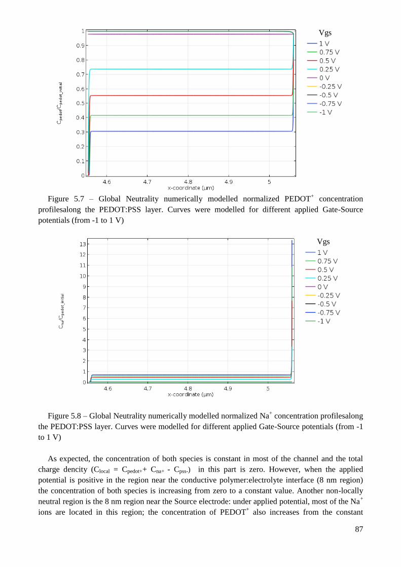
87
Vgs
Figure 5.7 – Global Neutrality numerically modelled normalized PEDOT+ concentration
profilesalong the PEDOT:PSS layer. Curves were modelled for different applied Gate-Source
potentials (from -1 to 1 V)
Vgs
Figure 5.8 – Global Neutrality numerically modelled normalized Na+ concentration profilesalong
the PEDOT:PSS layer. Curves were modelled for different applied Gate-Source potentials (from -1
to 1 V)
As expected, the concentration of both species is constant in most of the channel and the total
charge dencity (Clocal = Cpedot++ Cna+ - Cpss-) in this part is zero. However, when the applied
potential is positive in the region near the conductive polymer:electrolyte interface (8 nm region)
the concentration of both species is increasing from zero to a constant value. Another non-locally
neutral region is the 8 nm region near the Source electrode: under applied potential, most of the Na+
ions are located in this region; the concentration of PEDOT+ also increases from the constant

88
concentration region value to the initial concentration, equal to the concentration of PEDOT+
in a
fully doped channel state. In total, as expected, the region near the Source electrode has a very high
positive charge concentration.
Channel conductivity and Drain current calculation
From the values of σmax and P obtained, through the analytical model, the hole mobility could be
calculated following the equation:
𝜇 =𝜎𝑚𝑎𝑥
𝑃 ∙ 𝑞
(5.2)
Where q is the elementary charge.
Taking into account the constant mobility assumption and knowing the local concentration of
PEDOT+ makes a calculation of local conductivity, as well as an average channel conductivity,
possible:
𝜎𝑐ℎ =1
𝑑∙ ∫ 𝜎𝑙𝑑𝑥 =
1
𝑑∙ ∫ 𝑃𝑙𝑞𝜇 𝑑𝑥
𝑑
0
𝑑
0
(5.3)
Where σch, σl and Pl are the average channel conductivity, the local conductivity and the local
PEDOT+ density respectivly.
The average channel conductivity dependance on the applied potential is represented at the
Figure 5.9.
Figure 5.9 – Average channel conductivity dependance on applied voltage
0
2000
4000
6000
8000
10000
12000
-1.5 -1 -0.5 0 0.5 1 1.5 2 2.5
σ, S
/m
Vgs, V

89
From the Figure 5.9 above it is possible to conclude that the conductivity reaches the maximum
value 9892 S/m under slightly negative applied voltage and goes to a value very close to zero under
an applied voltage of about 1.5 V. All these results agree well with the prediction.
The newly gotten conductivity-applied voltage curves were used together with the gradual
channel approximation for the Drain current calculation according to equation 3.37. The result of
these calculations together with the experimentally obtaind Drain current – applied voltage profiles
is represented in Figures 5.10a. and b in the form of the output and transfer curves respectively.

90
a.
b.
Figure 5.10 – Drain current dependence on applied potential. Continuous line – calculated curve;
markers – experimental data points. a) Output curve (Drain current dependent on applied Drain-
Source potential for different Gate-Source potentials); b) Transfer curve (Drain current dependent
on applied Gate-Source potential for different Drain-Source potentials);
The Figures above show that there is a very good match between the experimentally measured
and the numerically modelled Drain current. Moreover the alignment between these two sets of
-0.003
-0.0025
-0.002
-0.0015
-0.001
-0.0005
0
0.0005
-0.65 -0.55 -0.45 -0.35 -0.25 -0.15 -0.05 0.05I d
, A
Vds, V
0 0.1 0.2 0.3 0.4 0.5 0.6
0 0.1 0.2 0.3 0.4 0.5 0.6
-0.003
-0.0025
-0.002
-0.0015
-0.001
-0.0005
0
0.0005
0 0.1 0.2 0.3 0.4 0.5 0.6 0.7
I d, A
Vgs, V
0 -0.1 -0.2 -0.3 -0.4 -0.5 -0.6
0 -0.1 -0.2 -0.3 -0.4 -0.5 -0.6Vds
Vgs

91
data is almost perfect for low applied Drain-Source potentials in the range between 0 and -0.3 V and
Gate-Source potentials between 0.1 and 0.3 V.
Conclusion
In Chapter 5, a complete cycle of calculations for the unique Organic Electrochemical transistor
was developed. Two types of analytical models fitting to experimental data allowed extracting the
set of the most important device parameters, such as maximum conductivity σmax, initial hole
density P, density of PSS-
Na, intrinsic charge carrier density ni and capacitance of PEDOT:PSS
layer Cd. These set of parameters permitted not only to characterize fully the device, but also to
check the validity of the Global Neutrality numerical model.
The derived maximum conductivity and initial holes density were used as the input parameters
for the numerical calculations performed with the COMSOL Multiphysics software. The result of
one dimensional model was local potential, PEDOT+ and Na
+ concentration profiles dependent on
the applied potential. Numerical model output was used for the channel conductivity calculations
dependent on the applied potential, which in its tern was used for the Drain current calculation. The
calculated Drain current–applied potential profile was compared with experimental profile, this
comparison allowed concluding that the Global Neutrality numerical model reflects very well the
real device behavior, so this model describes with no doubts the real physics and the chemistry of
an Organic Electrochemical Transistor.

92
CHAPTER 6. EXPERIMENTAL VALIDATION
Fabrication of the Organic Electrochemical Transistor
All OECT devices were fabricated in the cleanroom of Ecole Nationale Superieure des Mines de
Saint-Etienne with the kind help of Jonathan Rivnay, Jacob Friedlein and Professor George G.
Malliaras.
Organic Electrochemical Transistors were fabricated in a clean room by photolithography
process.[104] Fabrication process is similar to one described in the literature.[78] It consists of
several different materials patterning, such as perylene, metals and PEDOT:PSS. A typical
schematic architecture of the fabricated Organic Electrochemical Transistors is represented on the
in Figure 6.1.
Figure 6.1 – Schematic representation of Organic Electrochemical Transistor structure[43]
First of all glass slide substrates were cleaned by sonication in de-ionized water, acetone and
isopropyl alcohol with subsequent oxygen plasma treatment. The interconnects and the contacts
made of 5 nm of chromium and 100 nm of gold were patterned by the lift-off process. Channel of
the devices was made by spin coating a PEDOT:PSS mixture made of Clevios PH-1000, Heraeus
Holding GmbH aqueous dispersion with 5 % of ethylene glycol (EG), 0.1 % of dodecyl benzene
sulfonic acid (DBSA), and 1% of (3-glycidyloxypropyl) trimethoxysilane (3-GOPS). Dodecyl
benzene sulfonic acid was used for conductivity enhancement and 3-GOPS as crosslinking agent
that prevents film detachment from the substrate. After the spin-coating at 600–3000 rpm, the film
was baked at 100 °C for 90 seconds, followed by additional baking at 140 °C for 1 hour after the
peeling-off process. Devices were rinsed with deionized water to remove an anti-adhesive and non-
polymerized low molecular weight compounds.
Devices characterization was done using 100 mM NaCl solution as an electrolyte with the
Ag/AgCl wire electrode immersed inside. The Drain and Gate currents and applied potentials were
measured with NI-PXI-4071 and NI-PXI 6289 digital multimeters. Recorded signals were analyzed
with LabVIEW software customized by the user.
Moving Front Experiment
Experimental setup
To understand which of the two numerical models of PEDOT:PSS channel de-doping and ions
distribution is correct, devices were fabricated with the configuration shown in Figure 6.2.

93
a.
b.
Figure 6.2 – Device for steady state potential measurement of PEDOT:PSS channel under
applied gate-source potential: a) Simplified schematic representation; b) Real image
The device consisted of Ag/AgCl Gate electrode immersed in a well filled with the NaCl
electrolyte with concentration 100 mM; the PEDOT:PSS layer was connected to the electrolyte
layer at one side and to the gold Source electrode at the other side. Fourteen probe electrodes were
connected to the PEDOT:PSS layer at both sides of the channel to measure the electrical potential at
various distances from the Source electrode. Thus, the device allows measuring the potential along
the channel to compare the experimentally measured potential profile to that numerically calculated.
The device has the following geometrical characteristics: the thickness of PEDOT:PSS layer is
equal to 100 nm, the width – 200 µm and the length - 200 µm. This device was also used to
measure transient characteristics of the PEDOT:PSS layer under fixed applied potential.
Device fabrication and measurements
Glass substrates were cleaned thoroughly by ten minutes sonication in deionized water, in
acetone and finally in isopropanol. The Source electrode and the potential probe electrodes were
made of 5 nm of chromium and 100 nm of gold, patterned by the lift-off process. Standard
PEDOT:PSS mixture mentioned above (94% PH-1000, 5% EG, 1% 3-GOPS, 0.1% DBSA) was
spin coated in two layers. The first layer was spin coated in 3000 rpm and the baked at 70 °C for 90
seconds. The second layer of PEDOT:PSS was spin coated in 1000 rpm. Then the sample was
baked during 80 minutes at 130 °C. Epoxy-based photoresist SU-8 was patterned
photolithographicaly to cower most part of the channel and the Source electrode. The uncovered
part of PEDOT:PSS layer was connected with the electrolyte layer. Electrolyte was placed in a
PDMS well, covered with a glass lid. Two 2.5 mm x 2 mm Ag/AgCl pellets shorted together served
as a Gate electrode, were immersed into electrolyte.
Two opposite potential probe electrodes were shorted together for the channel potential
measurements. Gate-Source potential equal to 1V was applied along the device. Potential was
measured in seven points with different distances from the electrolyte during 100 seconds after
application of Gate-Source potential.
Pixel brightness was measured with a Point Grey GS3-U3-23S6M camera.

94
Theoretical potential profiles
In Chapter 3, we arrived at two very different types of profiles, depending onto whether ions are
“freely moving” (Global Neutrality model) or “locally trapped” (Local Neutrality model), (Figure
6.3).
a.
b.
Figure 6.3 – One dimensional numerically modeled profiles of electric potential in PEDOT:PSS
layer. Curves were modelled for different applied Gate-Source potentials (from 0 to 1 V): a) Local
neutrality model, Na+ ions are locally trapped in PEDOT:PSS; b) Global neutrality model, Na
+ ions
are free to move, but global neutrality of the layer is preserved
The geometry of the cell used to calculate the profiles in Figure 6.3 had the following
characteristics: NaCl 100 mM solution was used as an electrolyte, 200 µm long PEDOT:PSS layer
was used as a conductive polymer layer, with 1018
cm-3
initial holes density. Electrolyte-

95
PEDOT:PSS interface is located on the left side, PEDOT:PSS – Source interface is located on the
right side.
Experimentally measured profiles are expected to be similar to one of these two different
numerically modeled profiles. This similarity will indicate which one of two models is the correct
and realistic one.
Experimental results and discussion
Figure 6.4 shows an experimentally attained potential profile. The curve corresponds to a system
that has already reached the steady state. In practice, the profile was measured 200 sec. after the
Gate-Source potential was applied.
Figure 6.4 – Experimentally measured potential profile along PEDOT:PSS channel
From the Figures 6.3 and 6.4 above it is clear that the measured profile shows high similarity
with that modelled with the Global Neutrality assumption. It proves that the Global Neutrality
model is correct and reflects well the real situation in an Organic Electrochemical Transistor. The
difference between the calculated and measure values in the channel could be explained by the
difference between the real hole density and that used as an input for the numerical model. When
correcting this parameter, it is possible to get an almost perfect match between the numerically
modelled and the experimentally measured potential profiles (Figure 6.5).
-0.05
0
0.05
0.1
0.15
0.2
0.25
0.3
-50 0 50 100 150 200 250
Loca
l po
ten
tial
, V
Distance from the electrolyte, µm

96
Figure 6.5 – Experimentally measured (marked line) and numerically modelled (straight line)
potential profile along the PEDOT:PSS channel. Numerically modelled profile with different initial
holes concentration: A- 1018
cm-3
; B- 5·1018
cm-3
; C- 1019
cm-3
; D- 5·1019
cm-3
The Figure 6.5 clearly shows that potential profile in the channel depends not only on the applied
voltage, but also on the initial hole concentration. It is possible to conclude, that according to
potential matching between experimentally measured potential profile and numerically modelled
potential profile, the initial hole concentration is very close to 5·1019
cm-3
.
While the steady state measurements represent the final state of the system, the time dependent
experiment allows depicting how the steady state is reached. In case of an Organic Electrochemical
Transistor it is interesting to understand how the dedoping front moves and which is the limiting
step of the de-doping process. In Figure 6.6 the change of potential with time at different points of
the channel is shown.
0
0.2
0.4
0.6
0.8
1
1.2
-30 20 70 120 170 220
Loca
l po
ten
tial
, V
Distance from the electrolyte, µm
A B C D Experimental results

97
a.
b.
Figure 6.6 – Time dependent channel potential measurements, measured at different distances
from an electrolyte: A – 0 µm; B – 20.51 µm; C – 50.34 µm; D – 100.51 µm; E – 150 µm; F –
180.51 µm; G – 200.34 µm;
a) From 0 sec to 100 sec; b) Enlarged region from 0 sec to 1 sec
Voltage reaches its maximum value 2 seconds after the potential is applied, then it slightly
decreases during 8 sec and afterwards remains constant. The first steep increase of the potential till
maximum is due to the applied voltage and almost immediate PEDOT+ reduction reaction. The
following decrease is due to the migration Na+ ions and the following redistribution inside the
conductive polymer layer, which leads to a local potential modification. The fact that the potential
0.00
0.05
0.10
0.15
0.20
0.25
0.30
-10 10 30 50 70 90 110
Vo
ltag
e, V
Time, s
0.00
0.05
0.10
0.15
0.20
0.25
0.30
-0.05 0.15 0.35 0.55 0.75 0.95
Vo
ltag
e, V
Time, s A B C D E F G

98
remains constant during the remaining time is clear evidence that the system has reached steady
state.
PEDOT+ reduction could be also investigated optically, due to PEDOT photochromic properties
(Figure 2.14). The amount of reduced PEDOT along the channel could be evaluated by the
normalized pixel intensity (Figure 6.7).
Figure 6.7 – Normalized pixel intensity along the PEDOT:PSS channel, measured at different
times from 0 to 600 ms. Initial potential 0 V, applied potential 1V
Changing the potential from 0 to 1 V permits to observe the time-dependent variation in pixels
intensity correlated with the variation of reduced PEDOT concentration. Increasing the potential
from 0 to 1 V allows performing the classical moving front experiment.[91] These measurements
show that the reduction of PEDOT+ starts from the electrolyte layer. We note that after 200 ms the
reduction process has already occurred through the whole channel and that the system reached
steady state.
It is also possible to estimate the temporal evolution of the de-doping front, by measuring the
time dependent evolution of pixels with a particular normalized intensity. For this estimation a
normalized pixel with an average intensity equal to 10 was taken.
0
5
10
15
20
25
-10 10 30 50 70 90 110 130 150 170 190 210
No
rmal
ized
pix
el in
ten
sity
/8-b
its
Distance from electrolyte, um
0 20 40 60 80 100 200 600

99
Figure 6.8 – Temporal evolution of the redox front drift length
From the figure above it is possible to conclude that the de-doping front moves linearly with
time at least during the first 150 µs, this timing should mainly correspond to the first redox process
inside OECT, and thus hole movement.
a.
R² = 0.9902
0
20
40
60
80
100
120
140
160
0 20 40 60 80 100 120
Dis
tan
ce f
rom
ele
ctro
lyte
, um
Time, ms
Data points Trend line

100
b.
Figure 6.9 – PEDOT0
normalized concentration profile: a) Global Neutrality model; b)
EGOFET-like model
Experimentally obtained PEDOT0 profile (Figure 6.7) is comparable to one modeled with Global
Neutrality assumption (Figure 6.9a). From this comparison it is also necessary to note that PEDOT+
reduction process occurs together with electrolyte ions movement and ions are moving with the
speed of Moving front. If the ions would move slower than holes, the PEDOT0 profile would be
similar to one modeled with EGOFET-like structure (Figure 6.9b), which is not the case in the
reality.
Figure 6.10 – Squared temporal evolution of the redox front drift length
It is possible to calculate the mobility of the charge carriers responsible for the redox front
movement[46] by using the equation:
0
2000
4000
6000
8000
10000
12000
14000
0 20 40 60 80 100
Sqar
ed d
ista
nce
fro
m e
lect
roly
te,
µm
2
Time, ms
Data points Trend line

101
𝑙2 = 2𝜇𝑉𝑡
(6.1)
Where l is a drift length, µ -mobility of the charge carriers, V- the applied potential and t the
time.
So from the Figure 6.10 and Equation 6.1 the mobility is µ = 1·10-3 cm2/V·s , which is 20 times
higher than the previously reported value of Na+ mobility inside PEDOT:PSS layer (1.9·10-4
cm2/V·s)[46] and also higher than the value of electrophoretic mobility of Na+
in bulk water at the
infinite dilution limit (7.6·10-4 cm2/V·s)[105].
As a result, the mobility value and the transient
behavior curve allows to suppose that the Moving front experiment reflects the ionic motion due to
drift under high electric field as it was stated before.
Conclusion
Potential measurements were performed to validate which of the two numerical models,
described in the Chapter 3 is correct: the Local Neutrality model or the Global Neutrality model. As
a result it was shown that the Global Neutrality model potential profile matches very well the
experimentally measured potential profile, especially for hole concentration equal to 5·1019
cm-3
. As
a result, the Global Neutrality model could be successfully used for an explanation of an Organic
Electrochemical Transistor working principle. Spectroscopic measurements allowed following the
time-dependent reduction process of PEDOT:PSS; it was shown that the moving front travels
linearly with time and that the steady state is already reached after 2 seconds. The mobility of the
charge carriers was also extracted; very high mobility value and fast achievement of the steady state
allows to suppose that the Moving front experiment allows to observe holes extraction together with
ionic movement process inside PEDOT:PSS, as it was reported previously.

102
CHAPTER 7 CONCLUSION AND OUTLOOK
The work presented in the current thesis is dedicated to the Physical Modelling of biosensors
based on Organic Electrochemical Transistor. Two types of models were developed in the scope of
this thesis: numerical model and analytical model. Combining these two models it is possible not
only to describe the working principle of an OECT, but also to extract all the parameters needed to
characterize an already made device, which would lead to the optimization of the fabrication of
devices for any specific type of application.
The first part of the thesis aimed to describe the state of the art in the field of organic electronics,
bioelectronics, biosensors and in particular to emphasize on the importance and principle
advantages of Organic Electrochemical transistors among the other categories of biosensors.
The first chapter serves as an introduction to the field. Since 1954 when the first semiconducting
organic material was discovered and 1962 when the first biosensor was made, organic electronics
and bioelectronics has developed a lot. It was possible due to the advantages of organic in
comparison with inorganic materials, such as the ability to operate at low voltage, the ability to be
fabricated by low-cost printing techniques and the ability to conduct both ionic and electronic
charges. Nowadays different types of organic transistors are used in a huge variety of applications.
An OECT is a particular type of transistor based sensor that is widely used in biosensing and
medical applications. Being a three-terminal device, its working principle is based on Drain current
modulation under applied Gate-Source voltage due to redox de-doping of the conductive channel.
Despite the fact that Organic Electrochemical Transistors are widely used the mechanism of its core
de-doping process was not enough studied and described. To sum up first chapter aimed to make a
brief observation of the field of research for the further going to the subject of an investigation.
An explanation of the current state of the art in the field and the background information is very
important, being the starting point of any scientific research; it allows asking the important
questions to fill the gaps in the scientific knowledge. The chapter part is dedicated to the summary
of internal physics and chemistry of the device. Since an OECT consists of two main parts:
ionically conductive layer and electronically conductive layer, it is very important to explain the
properties of each layer. In most of the cases a highly diluted true electrolyte, such as NaCl solution
is used as an ionically conductive layer. This type of electrolyte is characterized by completely
dissolved positive and negative ions surrounded by a hydration shell. Ion-ion and ion-solvent
interactions take place in the solution, due to the fact that each hydrated ion is charged. Attractive
and repelling forces allow the ionic solution to maintain the local equilibrium. In the presence of an
electric field or concentration gradient ions move to maintain equilibrium, and if the electrode is
polarizable they form a double electrical layer at its interface. Therefore the balance between drift
and diffusion forces defines not only the equilibrium of the system, but it also generates an ionic
current.
The second active element in OECT is the electronically conductive layer. Conductive polymers,
such as PEDOT:PSS are often used for this. PEDOT:PSS is a holes transporting material and this
type of transport is also the result of two components: drift and diffusion. So the charge transport in
an electrolyte and in a conductive polymer could be described using the same set of equations:
Poisson-Boltzmann and Nernst-Planck equations. A separate description of the physics of each
active layer is important, but in an OECT these two layers are also interacting between each other
upon the application of Gate-Source voltage. First of all the reduction of PEDOT+ takes place, so
the amount of holes is decreasing, then the ions from the electrolyte penetrate inside to maintain
electrical neutrality. This process is called de-doping of the conductive polymer. The time evolution

103
of the process can be visualized by the so-called Moving front experiment. Being the core element
of OECT working principle, this process is the focal point of the thesis. As a result, a detailed
description of the state of the art of internal device physics is given in Chapter two.
First of all it is extremely important to understand and explain the OECT working principle and
the physics of the dedoping process. This is why the precise numerical modelling is an essential part
of the current thesis. The third Chapter is entirely dedicated to this type of one-dimensional
modelling. Two pictures for the distribution of ions inside the conductive polymer layer were
described, and thus two types of models made up. The first model is the Local Neutrality model, in
which ions percolating inside the conductive polymer layer are trapped inside to maintain local
electroneutrality. The second model is the Global neutrality model, when the ions are not locally
trapped, but they are moving freely inside the polymer layer, maintaining only global neutrality. As
a result of the modelling two sets of different local potential, PEDOT+ and Na
+ concentration
profiles were obtained and the conductivity curves were calculated accordingly. These curves
together with the gradual channel approximation allow calculating transfer and output
characteristics for a device modelled with any of the two models. The respective current profiles are
different for each model; for the Global Neutrality model the transistor becomes fully de-doped
upon the application of 1V Gate-Source potential. This makes the Global Neutrality model to be
more realistic. Moreover, to validate the model the experimental measurements of the local
potential of PEDOT:PSS layer were performed. A very good match was achieved between the
experimentally measured and the Global Neutrality numerically modelled potential profiles. Thus a
clear proof of the Global Neutrality model validity was shown in the Chapter seven.
Using the numerically modelled conductivity curves it is possible to set-up a parametric
analytical model, by fitting the curve to an analytical equation. The best function, which fits well
the numerically modelled Global Neutrality conductivity curve, is Boltzmann logistics function.
Therefore two possible one-dimensional models of an OECT were described in this chapter;
moreover the transfer from the fully numerical to the analytical model was successfully made.
While the numerical models are describing the working principle of any OECT device, analytical
models allow to extract the important parameters and to characterize the real OECT. The coupling
of two analytical models: the Boltzmann parametric model and the Conventional Semiconductor
model, allowed to extract the maximum conductivity of the fully doped PEDOT:PSS layer σmax, the
intrinsic charge carrier density ni, the PSS- density NA
-, the volumetric capacitance C
* and the initial
holes density pmax. This set of models could be used to characterize the Organic Electrochemical
Transistors with different channel sizes. In each case the models showed a very good fit to the
experimental Id – Vgs curve, characterized by PPMMCC ≥ 0.999. Despite of the parameters
extraction it is possible to use the analytical models for a device characterization. By applying the
Boltzmann parametric model to the set of transistors it was proven that the maximum conductivity
showed the correlation with the conductive channel geometry: the conductivity has the highest
value for the channels with high length to area ratio. This conclusion together with the other
extracted parameters could be used to fabricate optimal OECT devices for any type of application.
Lastly, having the Global Neutrality numerical model, the Boltzmann parametric analytical
model and the Conventional Semiconductor models it is possible to make the full characterization
for any OECT. An example of this characterization developed in Chapter 5. First of all it is
necessary to measure the Id-Vgs profile for Vds = -0.5 V. Fitting the experimental curve to the
Boltzmann parametric function leads to the value of σmax. This value was used to decrease the
number of Conventional Semiconductor model fitting parameters. Initial holes density pmax was
extracted as a result of the second analytical function fitting. The maximum conductivity value, the

104
initial holes density value and the size of the channel were then used as input parameters for Global
Neutrality numerical modelling of the OECT. The result of the modelling represented in the form of
transfer and output curves was compared to the experimental data. Very good match between these
two data sets allowed to conclude that all the models are valid and could be used to characterize an
OECT with a very high degree of precision.
Globally this thesis represents the modelling of an OECT from an electrochemical point of view.
Additional effort needs to be done to make the model more accurate. It is very important to take in
account the other processes, occurring inside OECT, such as the polymer chains transformation and
swelling, the possibility of Cl- ion penetration and the global conductive polymer interaction with
an electrolyte media. It is also very interesting to include the effects of the contact between
PEDOT:PSS layer and living cells culture, since an OECT is aimed to be used for invivo
applications.
To conclude, the theoretical modelling is a very powerful tool to explain the working principle of
an OECT and characterize the device. The usage the models is not only the matter of a global
understanding, but also it is a prominent step towards an optimal and efficient device creation.

105
List of publications
1. Shirinskaya, A., Horowitz, G., Bonnassieux, Y., Rivnay, J., Malliaras G., Analytical
modelling of the Organic Electrochemical Transistor, Advanced Functional Materials,
2017. (submitted)
2. Shirinskaya, A., et al. (2017) Numerical Modelling of Biosensors based on the Organic
Electrochemical Transistor (in preparation)

106
References
1. Akamatu, H., H. Inokuchi, and Y. Matsunaga, Electrical Conductivity of the Perylene-
Bromine Complex. Nature, 1954. 173(4395): p. 168-169.
2. Shaw, J.M. and P.F. Seidler, Organic electronics: Introduction. Ibm Journal of Research
and Development, 2001. 45(1): p. 3-9.
3. Skotheim, T.A., Handbook of conducting polymers. 1997: CRC press.
4. McNaught, A.D., Compendium of chemical terminology. Vol. 1669. 1997: Blackwell
Science Oxford.
5. Clark, L.C. and C. Lyons, Electrode systems for continuous monitoring in cardiovascular
surgery. Annals of the New York Academy of sciences, 1962. 102(1): p. 29-45.
6. Janata, J. and M. Josowicz, Conducting polymers in electronic chemical sensors. Nature
materials, 2003. 2(1): p. 19-24.
7. Bai, H. and G. Shi, Gas sensors based on conducting polymers. Sensors, 2007. 7(3): p. 267-
307.
8. Kergoat, L., et al., Advances in organic transistor-based biosensors: from organic
electrochemical transistors to electrolyte-gated organic field-effect transistors. Analytical
and bioanalytical chemistry, 2012. 402(5): p. 1813-1826.
9. Ferro, M. and G. Malliaras, Organic electrochemical transistor. 2015, Google Patents.
10. Magliulo, M., et al., Sensing & Measurement Ultrasensitive printable biosensors for point-
of-care applications.
11. Zhu, Z.-T., et al., A simple poly (3, 4-ethylene dioxythiophene)/poly (styrene sulfonic acid)
transistor for glucose sensing at neutral pH. Chemical Communications, 2004(13): p. 1556-
1557.
12. Macaya, D.J., et al., Simple glucose sensors with micromolar sensitivity based on organic
electrochemical transistors. Sensors and Actuators B: Chemical, 2007. 123(1): p. 374-378.
13. Bernards, D.A., et al., Enzymatic sensing with organic electrochemical transistors. Journal
of Materials Chemistry, 2008. 18(1): p. 116-120.
14. Jia, W., et al., Electrochemical tattoo biosensors for real-time noninvasive lactate
monitoring in human perspiration. Analytical Chemistry, 2013. 85(14): p. 6553-6560.
15. Tarabella, G., et al., Liposome sensing and monitoring by organic electrochemical
transistors integrated in microfluidics. Biochimica et Biophysica Acta (BBA)-General
Subjects, 2013. 1830(9): p. 4374-4380.
16. Tang, H., et al., Highly sensitive dopamine biosensors based on organic electrochemical
transistors. Biosensors and Bioelectronics, 2011. 26(11): p. 4559-4563.
17. Lin, P., et al., Organic electrochemical transistors integrated in flexible microfluidic
systems and used for label‐free DNA sensing. Advanced Materials, 2011. 23(35): p. 4035-
4040.
18. Someya, T., et al., Integration and response of organic electronics with aqueous
microfluidics. Langmuir, 2002. 18(13): p. 5299-5302.
19. Magliulo, M., et al., Part per trillion label-free electronic bioanalytical detection. Analytical
Chemistry, 2013. 85(8): p. 3849-3857.
20. Magliulo, M., et al., Electrolyte‐Gated Organic Field‐Effect Transistor Sensors Based on
Supported Biotinylated Phospholipid Bilayer. Advanced Materials, 2013. 25(14): p. 2090-
2094.
21. Lin, T.-W., D. Kekuda, and C.-W. Chu, Label-free detection of DNA using novel organic-

107
based electrolyte-insulator-semiconductor. Biosensors and Bioelectronics, 2010. 25(12): p.
2706-2710.
22. Kergoat, L., et al., DNA detection with a water-gated organic field-effect transistor. Organic
Electronics, 2012. 13(1): p. 1-6.
23. Loi, A., I. Manunza, and A. Bonfiglio, Flexible, organic, ion-sensitive field-effect transistor.
Applied Physics Letters, 2005. 86(10): p. 103512.
24. Bartic, C., et al., Monitoring pH with organic-based field-effect transistors. Sensors and
Actuators B: Chemical, 2002. 83(1): p. 115-122.
25. Diallo, A., et al., Trimethylamine biosensor based on pentacene enzymatic organic field
effect transistor. Applied Physics Letters, 2009. 94(26): p. 176.
26. Liu, J., M. Agarwal, and K. Varahramyan, Glucose sensor based on organic thin film
transistor using glucose oxidase and conducting polymer. Sensors and Actuators B:
Chemical, 2008. 135(1): p. 195-199.
27. Huang, W., et al., Label-free brain injury biomarker detection based on highly sensitive
large area organic thin film transistor with hybrid coupling layer. Chemical Science, 2014.
5(1): p. 416-426.
28. Khan, H.U., et al., Effect of passivation on the sensitivity and stability of pentacene
transistor sensors in aqueous media. Biosensors and Bioelectronics, 2011. 26(10): p. 4217-
4221.
29. Khan, H.U., et al., In situ antibody detection and charge discrimination using aqueous
stable pentacene transistor biosensors. Journal of the American Chemical Society, 2011.
133(7): p. 2170-2176.
30. Spijkman, M.J., et al., Dual‐gate organic field‐effect transistors as potentiometric sensors in
aqueous solution. Advanced Functional Materials, 2010. 20(6): p. 898-905.
31. Khan, H.U., et al., In Situ, Label‐Free DNA Detection Using Organic Transistor Sensors.
Advanced Materials, 2010. 22(40): p. 4452-4456.
32. Khan, H.U., et al., The effect of pH and DNA concentration on organic thin-film transistor
biosensors. Organic Electronics, 2012. 13(3): p. 519-524.
33. Elkington, D., et al., Organic thin-film transistor (OTFT)-based sensors. Electronics, 2014.
3(2): p. 234-254.
34. Głowacki, E.D., et al., Hydrogen‐Bonded Semiconducting Pigments for Air‐Stable Field‐
Effect Transistors. Advanced Materials, 2013. 25(11): p. 1563-1569.
35. Stoliar, P., et al., DNA adsorption measured with ultra-thin film organic field effect
transistors. Biosensors and Bioelectronics, 2009. 24(9): p. 2935-2938.
36. Maddalena, F., et al., Organic field-effect transistor-based biosensors functionalized with
protein receptors. Journal of Applied Physics, 2010. 108(12): p. 124501.
37. Roberts, M.E., et al., Water-stable organic transistors and their application in chemical and
biological sensors. Proceedings of the National Academy of Sciences, 2008. 105(34): p.
12134-12139.
38. Torsi, L., et al., Organic field-effect transistor sensors: a tutorial review. Chemical Society
Reviews, 2013. 42(22): p. 8612-8628.
39. Schöning, M.J. and A. Poghossian, Recent advances in biologically sensitive field-effect
transistors (BioFETs). Analyst, 2002. 127(9): p. 1137-1151.
40. Hütter, P.C., et al., Influence of geometry variations on the response of organic
electrochemical transistors. Applied Physics Letters, 2013. 103(4): p. -.
41. Strakosas, X., M. Bongo, and R.M. Owens, The organic electrochemical transistor for

108
biological applications. Journal of Applied Polymer Science, 2015. 132(15).
42. Kim, Y., et al., A glucose sensor based on an organic electrochemical transistor structure
using a vapor polymerized poly (3, 4-ethylenedioxythiophene) layer. Japanese Journal of
Applied Physics, 2010. 49(1S): p. 01AE10.
43. Khodagholy, D., et al., High transconductance organic electrochemical transistors. Nature
Communications, 2013. 4.
44. Kumar, A. and J. Sinha, Electrochemical Transistors for Applications in Chemical and
Biological Sensing, in Organic Semiconductors in Sensor Applications, D.A. Bernards, G.G.
Malliaras, and R.M. Owens, Editors. 2008, Springer Berlin Heidelberg: Berlin, Heidelberg.
p. 245-261.
45. Yaghmazadeh, O., et al., Optimization of Organic Electrochemical Transistors for Sensor
Applications. Journal of Polymer Science Part B-Polymer Physics, 2011. 49(1): p. 34-39.
46. Stavrinidou, E., et al., A simple model for ion injection and transport in conducting
polymers. Journal of Applied Physics, 2013. 113(24).
47. Bernards, D.A. and G.G. Malliaras, Steady-state and transient behavior of organic
electrochemical transistors. Advanced Functional Materials, 2007. 17(17): p. 3538-3544.
48. Yang, S.Y., et al., Electrochemical transistors with ionic liquids for enzymatic sensing.
Chemical Communications, 2010. 46(42): p. 7972-7974.
49. Khodagholy, D., et al., Organic electrochemical transistor incorporating an ionogel as a
solid state electrolyte for lactate sensing. Journal of Materials Chemistry, 2012. 22(10): p.
4440-4443.
50. Lin, P., et al., The Application of Organic Electrochemical Transistors in Cell‐Based
Biosensors. Advanced Materials, 2010. 22(33): p. 3655-3660.
51. Bolin, M.H., et al., Active Control of Epithelial Cell‐Density Gradients Grown Along the
Channel of an Organic Electrochemical Transistor. Advanced Materials, 2009. 21(43): p.
4379-4382.
52. Khodagholy, D., et al., In vivo recordings of brain activity using organic transistors. Nature
Communications, 2013. 4: p. 1575.
53. Bockris, J., ’M. and Reddy, AKN (1970) Modern Electrochemistry, Vol. 1. Macdonald,
London. 125.
54. Brown, T.L., et al., Chemistry: the central science. Vol. 8. 1994: Prentice Hall Englewood
Cliffs, NJ.
55. Hückel, E. and P. Debye, The theory of electrolytes: I. lowering of freezing point and
related phenomena. Phys. Z, 1923. 24: p. 185-206.
56. Bard, A.J., Electrochemical methods. Fundamentals and applications. 2001: John Wiley &
Sons. 833.
57. Butt, H.-J., K. Graf, and M. Kappl, Physics and chemistry of interfaces. 2006: John Wiley &
Sons.
58. Wright, M.R., An introduction to aqueous electrolyte solutions. 2007: John Wiley & Sons.
59. Einstein, A., Un the movement of small particles suspended in statiunary liquids required by
the molecular-kinetic theory 0f heat. Ann. d. Phys, 1905. 17: p. 549-560.
60. Bard, A.J., et al., Electrochemical methods: fundamentals and applications. Vol. 2. 1980:
Wiley New York.
61. Khodagholy, D., et al., High transconductance organic electrochemical transistors. Nature
Communications, 2013. 4.
62. Chen, S., Y. Liu, and J. Chen, Heterogeneous electron transfer at nanoscopic electrodes:

109
importance of electronic structures and electric double layers. Chemical Society Reviews,
2014. 43(15): p. 5372-5386.
63. Nalwa, H.S., Handbook of Organic Conductive Molecules and Polymers, Volume 4,
Conductive Polymers: Transport, Photophysics and Applications. 1997: John Wiley & Sons
Ltd: Baffins Lane, Chichester, West Sussex PO19 IUD, England.
64. Blaha, K., Iupac Recommendation - Nomenclature of Inorganic-Chemistry (the Red Book) -
Revision of 2nd Edition (1970). Chemicke Listy, 1987. 81(2): p. 206-207.
65. Pauling, L., The nature of the chemical bond and the structure of molecules and crystals: an
introduction to modern structural chemistry. Vol. 18. 1960: Cornell university press.
66. Moore, J., C. Stanitski, and P. Jurs, Principles of chemistry: the molecular science. 2009:
Cengage Learning.
67. Nardes, A.M., On the conductivity of PEDOT: PSS thin films. Technische Universiteit
Eindhoven. Eindhoven, 2007: p. 132.
68. Banerji, A., M.W. Tausch, and U. Scherf, Classroom Experiments and Teaching Materials
on OLEDs with Semiconducting Polymers. Educación Química, 2013. 24(1): p. 17-22.
69. Amitabh, B., M.W. Tausch, and U. Scherf, Classroom Experiments and Teaching Materials
on OLEDs with Semiconducting Polymers. Educación Química. 24(1).
70. Martínez, J.G., J. Arias-Pardilla, and T.F. Otero, Simultaneous Smart Actuating-Sensing
Devices Based on Conducting Polymers. 2012: INTECH Open Access Publisher.
71. Martínez, J.G., J. Arias-Pardilla, and T.F. Otero, Simultaneous Smart Actuating-Sensing
Devices Based on Conducting Polymers, in Smart Actuation and Sensing Systems-Recent
Advances and Future Challenges. 2012, InTech.
72. Bredas, J.L. and G.B. Street, Polarons, bipolarons, and solitons in conducting polymers.
Accounts of Chemical Research, 1985. 18(10): p. 309-315.
73. Fazzi, D. and M. Caironi, Multi-length-scale relationships between the polymer molecular
structure and charge transport: the case of poly-naphthalene diimide bithiophene. Physical
Chemistry Chemical Physics, 2015. 17(14): p. 8573-8590.
74. Yamato, H., M. Ohwa, and W. Wernet, Stability of polypyrrole and poly (3, 4-
ethylenedioxythiophene) for biosensor application. Journal of Electroanalytical Chemistry,
1995. 397(1-2): p. 163-170.
75. Shim, N.Y., et al., All-Plastic Electrochemical Transistor for Glucose Sensing Using a
Ferrocene Mediator. Sensors, 2009. 9(12): p. 9896-9902.
76. Elschner, A., et al., PEDOT. Principles and Applications of an Intrinsically Conductive
Polymer, 2011.
77. Horii, T., et al., Correlation between the hierarchical structure and electrical conductivity of
PEDOT/PSS. Polymer Journal, 2015. 47(10): p. 695-699.
78. Rivnay, J., et al., Organic electrochemical transistors with maximum transconductance at
zero gate bias. Advanced Materials, 2013. 25(48): p. 7010-7014.
79. Rivnay, J., et al., Structural control of mixed ionic and electronic transport in conducting
polymers. Nature Communications, 2016. 7.
80. Nardes, A.M., et al., Conductivity, work function, and environmental stability of PEDOT:
PSS thin films treated with sorbitol. Organic Electronics, 2008. 9(5): p. 727-734.
81. Alemu, D., et al., Highly conductive PEDOT: PSS electrode by simple film treatment with
methanol for ITO-free polymer solar cells. Energy & environmental science, 2012. 5(11): p.
9662-9671.
82. Kim, Y.H., et al., Highly conductive PEDOT: PSS electrode with optimized solvent and

110
thermal post‐treatment for ITO‐free organic solar cells. Advanced Functional Materials,
2011. 21(6): p. 1076-1081.
83. Kawahara, J., et al., Improving the color switch contrast in PEDOT: PSS-based
electrochromic displays. Organic Electronics, 2012. 13(3): p. 469-474.
84. Tarabella, G., et al., Organic electrochemical transistors monitoring micelle formation.
Chemical Science, 2012. 3(12): p. 3432-3435.
85. Lock, J.P., et al., Electrochemical investigation of PEDOT films deposited via CVD for
electrochromic applications. Synthetic Metals, 2007. 157(22): p. 894-898.
86. Nernst, W., Theorie der Reaktionsgeschwindigkeit in heterogenen Systemen. Zeitschrift für
physikalische Chemie, 1904. 47(1): p. 52-55.
87. Kirchmeyer, S. and K. Reuter, Scientific importance, properties and growing applications of
poly (3, 4-ethylenedioxythiophene). Journal of Materials Chemistry, 2005. 15(21): p. 2077-
2088.
88. Park, H.-S., et al., Redox-active charge carriers of conducting polymers as a tuner of
conductivity and its potential window. Scientific Reports, 2013. 3.
89. Prigodin, V., et al., Electric field control of charge transport in doped polymers. Synthetic
Metals, 2005. 153(1-3): p. 157-160.
90. Robinson, N.D., et al., On the current saturation observed in electrochemical polymer
transistors. Journal of the Electrochemical Society, 2006. 153(3): p. H39-H44.
91. Stavrinidou, E., et al., Direct Measurement of Ion Mobility in a Conducting Polymer.
Advanced Materials, 2013. 25(32): p. 4488-4493.
92. Available from: https://www.comsol.com.
93. Panzer, M.J. and C.D. Frisbie, Exploiting Ionic Coupling in Electronic Devices: Electrolyte‐
Gated Organic Field‐Effect Transistors. Advanced Materials, 2008. 20(16): p. 3177-3180.
94. Weis, M., Gradual channel approximation models for organic field-effect transistors: The
space-charge field effect. Journal of Applied Physics, 2012. 111(5): p. 054506.
95. Tanase, C., et al., Unification of the Hole Transport in Polymeric Field-Effect Transistors
and Light-Emitting Diodes. Physical Review Letters, 2003. 91(21): p. 216601.
96. Pasveer, W.F., et al., Unified description of charge-carrier mobilities in disordered
semiconducting polymers. Physical Review Letters, 2005. 94(20): p. 206601.
97. McGarry, S.P. and N.G. Tarr, Fabrication and modelling of screen-printed active
electrolytic polymer devices. Semiconductor Science and Technology, 2008. 23(5).
98. Crispin, X., et al., The origin of the high conductivity of poly (3, 4-ethylenedioxythiophene)-
poly (styrenesulfonate)(PEDOT-PSS) plastic electrodes. Chemistry of Materials, 2006.
18(18): p. 4354-4360.
99. Sze, S.M. and K.K. Ng, Physics of semiconductor devices. 2006: John wiley & sons.
100. Groenendaal, L., et al., poly (3, 4‐ethylenedioxythiophene) and its derivatives: past, present,
and future. Advanced Materials, 2000. 12(7): p. 481-494.
101. Volkov, A.V., et al., Understanding the Capacitance of PEDOT: PSS. Advanced Functional
Materials, 2017.
102. Rivnay, J., et al., High-performance transistors for bioelectronics through tuning of channel
thickness. Science advances, 2015. 1(4): p. e1400251.
103. Kurra, N., J. Park, and H.N. Alshareef, A conducting polymer nucleation scheme for
efficient solid-state supercapacitors on paper. Journal of Materials Chemistry A, 2014.
2(40): p. 17058-17065.
104. DeFranco, J.A., et al., Photolithographic patterning of organic electronic materials. Organic

111
Electronics, 2006. 7(1): p. 22-28.
105. Atkins, P., Paula J. Atkins' physical chemistry. 2006, New York: WH Freeman and
Company.

112
Titre : Modelisation physique des biocapteurs au base des transisteurs electrochimiques
Mots clés : Électronique organique, bioélectronique, physique des appareils, transistor
electrochimique organique, dopage, modélisation numérique, modélisation analytique
Résumé : Les Transistors Organiques
Electrochimiques (OECT) sont largement
utilisés comme les capteurs dans de nombreux
appareils bioélectroniques.
Cette thèse est consacrée à la modélisation des
Transistors Organiques Electrochimiques. Tout
d'abord, un modèle d'état stationnaire
numérique a été établi. Il a été prouvé
expérimentalement que le modèle numérique dit
de «neutralité global» est valable pour expliciter
le fonctionnement global du capteur, mais aussi,
l'origine et le résultat du processus du dé-
dopage. La transition d’un modèle totalement
numérique à un modèle analytique a été réalisée
en ajustant la fonction analytique logistique
paramétrique de Boltzmann au profil de
conductivité calculé numériquement.
Il est possible d'extraire, en utilisant la valeur de
conductivité maximale et un modèle de semi-
conducteur conventionnel, les autres paramètres
pour la description complète d’OECT: densité
intrinsèque de charge, densité de trous initiaux,
concentration initiale de PSS- et capacité
volumétrique de la couche polymère
conductrice. Le fait d'avoir un outil permettant
d'extraire et de caractériser facilement tous les
OECT permet non seulement d'augmenter le
niveau de description de compréhension du
transistor, mais surtout de mieux maitriser la
corrélation entre paramètres internes et
externes.
En outre nous avons pu valider
expérimentalement la pertinence de nos
modèles en les comparants avec les
caractéristiques obtenues via des mesures
réelles.
Title : Physical modeling of biosensors based on organic electrochemical transistors
Keywords : organic electronics, bioelectronics, device physics, organic electrochemical transistor,
de-doping, numerical modelling, analytical modelling
Abstract: Organic Electrochemical Transistors
are widely used as transducers for sensors in
bioelectronics devices.
This thesis is dedicated to Organic
Electrochemical Transistors modelling. First of
all, a numerical steady state model was
established. Two numerical models were
proposed. In the first, Local Neutrality model,
the assumption of electrolyte ions trapping in
PEDOT:PSS layer was taken into
consideration, thus the local neutrality was
preserved. In the second model the ions were
allowed to move freely under applied electric
field inside conductive polymer layer, thus only
global electroneutrality was kept. It was
experimentally proven that the Global
Neutrality numerical model is valid to explain
the global physics of the device, the origin and
the result of the de-doping process. The
transition from totally numerical model to
analytical model was performed by fitting the
parametric analytical Boltzmann logistic
function to numerically calculated conductivity
profiles. As a result, an analytical equation for
the Drain current dependence on applied
voltage was derived and maximum
conductivity value was calculated. Using the
maximum conductivity value together with the
Conventional Semiconductor model it is
possible to extract the other parameters for the
full description of the OECT. Having a tool to
make easy parameters extraction and
characterization of any OECT, permits not only
to increase the level of device description, but most importantly to highlight the correlation
between external and internal device
parameters.
As a result, not only the purely theoretical
model was presented in this thesis to describe
the device physics, but also the prominent step
was made on simple real device
characterization.

113