pic10f200/202/204/206 6-pin, 8-bit flash …ww1.microchip.com/downloads/en/devicedoc/41239a.pdf2004...
TRANSCRIPT

2004 Microchip Technology Inc. Preliminary DS41239A
PIC10F200/202/204/206Data Sheet
6-Pin, 8-Bit Flash Microcontrollers

Note the following details of the code protection feature on Microchip devices:
• Microchip products meet the specification contained in their particular Microchip Data Sheet.
• Microchip believes that its family of products is one of the most secure families of its kind on the market today, when used in the intended manner and under normal conditions.
• There are dishonest and possibly illegal methods used to breach the code protection feature. All of these methods, to our knowledge, require using the Microchip products in a manner outside the operating specifications contained in Microchip’s Data Sheets. Most likely, the person doing so is engaged in theft of intellectual property.
• Microchip is willing to work with the customer who is concerned about the integrity of their code.
• Neither Microchip nor any other semiconductor manufacturer can guarantee the security of their code. Code protection does not mean that we are guaranteeing the product as “unbreakable.”
Code protection is constantly evolving. We at Microchip are committed to continuously improving the code protection features of ourproducts. Attempts to break Microchip’s code protection feature may be a violation of the Digital Millennium Copyright Act. If such actsallow unauthorized access to your software or other copyrighted work, you may have a right to sue for relief under that Act.
Information contained in this publication regarding deviceapplications and the like is intended through suggestion onlyand may be superseded by updates. It is your responsibility toensure that your application meets with your specifications.No representation or warranty is given and no liability isassumed by Microchip Technology Incorporated with respectto the accuracy or use of such information, or infringement ofpatents or other intellectual property rights arising from suchuse or otherwise. Use of Microchip’s products as criticalcomponents in life support systems is not authorized exceptwith express written approval by Microchip. No licenses areconveyed, implicitly or otherwise, under any intellectualproperty rights.
DS41239A-page ii Prelimin
Trademarks
The Microchip name and logo, the Microchip logo, Accuron, dsPIC, KEELOQ, microID, MPLAB, PIC, PICmicro, PICSTART, PRO MATE, PowerSmart, rfPIC, and SmartShunt are registered trademarks of Microchip Technology Incorporated in the U.S.A. and other countries.
AmpLab, FilterLab, MXDEV, MXLAB, PICMASTER, SEEVAL, SmartSensor and The Embedded Control Solutions Company are registered trademarks of Microchip Technology Incorporated in the U.S.A.
Analog-for-the-Digital Age, Application Maestro, dsPICDEM, dsPICDEM.net, dsPICworks, ECAN, ECONOMONITOR, FanSense, FlexROM, fuzzyLAB, In-Circuit Serial Programming, ICSP, ICEPIC, Migratable Memory, MPASM, MPLIB, MPLINK, MPSIM, PICkit, PICDEM, PICDEM.net, PICLAB, PICtail, PowerCal, PowerInfo, PowerMate, PowerTool, rfLAB, rfPICDEM, Select Mode, Smart Serial, SmartTel and Total Endurance are trademarks of Microchip Technology Incorporated in the U.S.A. and other countries.
SQTP is a service mark of Microchip Technology Incorporated in the U.S.A.
All other trademarks mentioned herein are property of their respective companies.
© 2004, Microchip Technology Incorporated, Printed in the U.S.A., All Rights Reserved.
Printed on recycled paper.
ary 2004 Microchip Technology Inc.
Microchip received ISO/TS-16949:2002 quality system certification for its worldwide headquarters, design and wafer fabrication facilities in Chandler and Tempe, Arizona and Mountain View, California in October 2003. The Company’s quality system processes and procedures are for its PICmicro® 8-bit MCUs, KEELOQ® code hopping devices, Serial EEPROMs, microperipherals, nonvolatile memory and analog products. In addition, Microchip’s quality system for the design and manufacture of development systems is ISO 9001:2000 certified.

PIC10F200/202/204/2066-Pin, 8-Bit Flash Microcontrollers
Devices Included In This Data Sheet:
• PIC10F200
• PIC10F202• PIC10F204• PIC10F206
High-Performance RISC CPU:
• Only 33 single-word instructions to learn
• All single-cycle instructions except for program branches, which are two-cycle
• 12-bit wide instructions• 2-level deep hardware stack• Direct, Indirect and Relative Addressing modes
for data and instructions• 8-bit wide data path
• 8 Special Function Hardware registers• Operating speed:
- 4 MHz internal clock
- 1 µs instruction cycle
Special Microcontroller Features:
• 4 MHz precision internal oscillator:- Factory calibrated to ±1%
• In-Circuit Serial Programming™ (ICSP™)
• In-Circuit Debugging (ICD) support• Power-on Reset (POR)• Device Reset Timer (DRT)
• Watchdog Timer (WDT) with dedicated on-chip RC oscillator for reliable operation
• Programmable code protection• Multiplexed MCLR input pin• Internal weak pull-ups on I/O pins
• Power-saving Sleep mode• Wake-up from Sleep on pin change
Low-Power Features/CMOS Technology:
• Operating Current:
- < 350 µA @ 2V, 4 MHz• Standby Current:
- 100 nA @ 2V, typical
• Low-power, high-speed Flash technology:- 100,000 Flash endurance - > 40 year retention
• Fully static design• Wide operating voltage range: 2.0V to 5.5V• Wide temperature range:
- Industrial: -40°C to +85°C- Extended: -40°C to +125°C
Peripheral Features (PIC10F200/202):
• 4 I/O pins:- 3 I/O pins with individual direction control
- 1 input only pin - High current sink/source for direct LED drive- Wake-on-change
- Weak pull-ups• 8-bit real-time clock/counter (TMR0) with 8-bit
programmable prescaler
Peripheral Features (PIC10F204/206):
• 4 I/O pins:- 3 I/O pins with individual direction control- 1 input only pin
- High current sink/source for direct LED drive- Wake-on-change- Weak pull-ups
• 8-bit real-time clock/counter (TMR0) with 8-bit programmable prescaler
• 1 Comparator- Internal absolute voltage reference- Both comparator inputs visible externally
- Comparator output visible externally
2004 Microchip Technology Inc. Preliminary DS41239A-page 1
PIC10F200/202/204/206
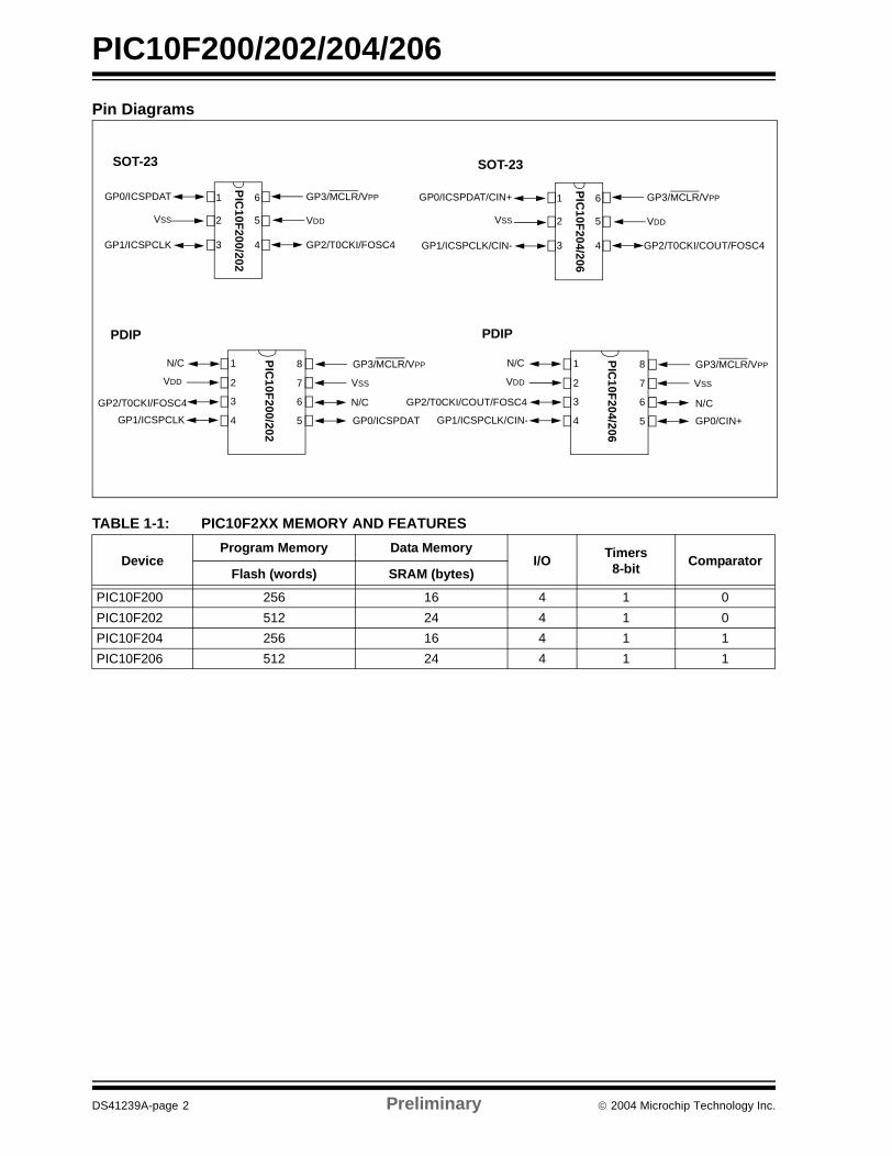
Pin Diagrams
TABLE 1-1: PIC10F2XX MEMORY AND FEATURES
DeviceProgram Memory Data Memory
I/OTimers
8-bitComparator
Flash (words) SRAM (bytes)
PIC10F200 256 16 4 1 0
PIC10F202 512 24 4 1 0
PIC10F204 256 16 4 1 1
PIC10F206 512 24 4 1 1P
IC10F
200/202
1
2
3
6
5
4
GP0/ICSPDAT
VSS
GP1/ICSPCLK
GP3/MCLR/VPP
VDD
GP2/T0CKI/FOSC4
SOT-23
PIC
10F204/206
1
2
3
6
5
4
GP0/ICSPDAT/CIN+
VSS
GP1/ICSPCLK/CIN-
GP3/MCLR/VPP
VDD
GP2/T0CKI/COUT/FOSC4
SOT-23
GP2/T0CKI/FOSC4
N/C
N/C
N/C
N/CGP2/T0CKI/COUT/FOSC4
PDIP PDIP
PIC
10F200/202
1
2
3
4
8
7
6
5
VDD
GP3/MCLR/VPP
VSS
GP0/ICSPDATGP1/ICSPCLK
PIC
10F204/206
1
2
3
4
8
7
6
5
VDD
GP3/MCLR/VPP
VSS
GP0/CIN+GP1/ICSPCLK/CIN-
DS41239A-page 2 Preliminary 2004 Microchip Technology Inc.

PIC10F200/202/204/206
Table of Contents
1.0 General Description...................................................................................................................................................................... 52.0 PIC10F200/202/204/206 Device Varieties .................................................................................................................................. 73.0 Architectural Overview ................................................................................................................................................................. 94.0 Memory Organization ................................................................................................................................................................. 155.0 I/O Port ....................................................................................................................................................................................... 256.0 Timer0 Module and TMR0 Register (PIC10F200/202)............................................................................................................... 297.0 Timer0 Module and TMR0 Register (PIC10F204/206)............................................................................................................... 338.0 Comparator Module.................................................................................................................................................................... 379.0 Special Features of the CPU...................................................................................................................................................... 4110.0 Instruction Set Summary ............................................................................................................................................................ 5111.0 Development Support................................................................................................................................................................. 5912.0 Electrical Characteristics ............................................................................................................................................................ 6513.0 DC and AC Characteristics Graphs and Charts ......................................................................................................................... 7514.0 Packaging Information................................................................................................................................................................ 77Index .................................................................................................................................................................................................... 81On-Line Support................................................................................................................................................................................... 83Systems Information and Upgrade Hot Line ........................................................................................................................................ 83Reader Response ................................................................................................................................................................................ 84Product Identification System .............................................................................................................................................................. 85
TO OUR VALUED CUSTOMERS
It is our intention to provide our valued customers with the best documentation possible to ensure successful use of your Micro-chip products. To this end, we will continue to improve our publications to better suit your needs. Our publications will be refinedand enhanced as new volumes and updates are introduced.
If you have any questions or comments regarding this publication, please contact the Marketing Communications Department viaE-mail at [email protected] or fax the Reader Response Form in the back of this data sheet to (480) 792-4150.We welcome your feedback.
Most Current Data SheetTo obtain the most up-to-date version of this data sheet, please register at our Worldwide Web site at:
http://www.microchip.com
You can determine the version of a data sheet by examining its literature number found on the bottom outside corner of any page.The last character of the literature number is the version number, (e.g., DS30000A is version A of document DS30000).
ErrataAn errata sheet, describing minor operational differences from the data sheet and recommended workarounds, may exist for currentdevices. As device/documentation issues become known to us, we will publish an errata sheet. The errata will specify the revisionof silicon and revision of document to which it applies.
To determine if an errata sheet exists for a particular device, please check with one of the following:
• Microchip’s Worldwide Web site; http://www.microchip.com• Your local Microchip sales office (see last page)• The Microchip Corporate Literature Center; U.S. FAX: (480) 792-7277When contacting a sales office or the literature center, please specify which device, revision of silicon and data sheet (include lit-erature number) you are using.
Customer Notification SystemRegister on our web site at www.microchip.com/cn to receive the most current information on all of our products.
2004 Microchip Technology Inc. Preliminary DS41239A-page 3

PIC10F200/202/204/206
NOTES:
DS41239A-page 4 Preliminary 2004 Microchip Technology Inc.
PIC10F200/202/204/206
1.0 GENERAL DESCRIPTION
The PIC10F200/202/204/206 devices from MicrochipTechnology are low-cost, high-performance, 8-bit, fully-static, Flash-based CMOS microcontrollers. Theyemploy a RISC architecture with only 33 single-word/single-cycle instructions. All instructions are singlecycle (1 µs) except for program branches, which taketwo cycles. The PIC10F200/202/204/206 devicesdeliver performance in an order of magnitude higherthan their competitors in the same price category. The12-bit wide instructions are highly symmetrical, result-ing in a typical 2:1 code compression over other 8-bitmicrocontrollers in its class. The easy to use and easyto remember instruction set reduces development timesignificantly.
The PIC10F200/202/204/206 products are equippedwith special features that reduce system cost andpower requirements. The Power-on Reset (POR) andDevice Reset Timer (DRT) eliminate the need forexternal Reset circuitry. INTRC Internal Oscillatormode is provided, thereby preserving the limitednumber of I/O available. Power-saving Sleep mode,Watchdog Timer and code protection features improvesystem cost, power and reliability.
The PIC10F200/202/204/206 devices are available incost-effective Flash, which is suitable for production inany volume. The customer can take full advantage ofMicrochip’s price leadership in Flash programmablemicrocontrollers, while benefiting from the Flashprogrammable flexibility.
The PIC10F200/202/204/206 products are supportedby a full-featured macro assembler, a software simula-tor, an in-circuit debugger, a ‘C’ compiler, a low-costdevelopment programmer and a full featured program-mer. All the tools are supported on IBM® PC andcompatible machines.
1.1 Applications
The PIC10F200/202/204/206 devices fit in applicationsranging from personal care appliances and securitysystems to low-power remote transmitters/receivers.The Flash technology makes customizing applicationprograms (transmitter codes, appliance settings,receiver frequencies, etc.) extremely fast and conve-nient. The small footprint packages, for through hole orsurface mounting, make these microcontrollers wellsuited for applications with space limitations. Low cost,low power, high performance, ease of use and I/Oflexibility make the PIC10F200/202/204/206 devicesvery versatile even in areas where no microcontrolleruse has been considered before (e.g., timer functions,logic and PLDs in larger systems and coprocessorapplications).
TABLE 1-1: PIC10F200/202/204/206 DEVICES PIC10F200 PIC10F202 PIC10F204 PIC10F206
Clock Maximum Frequency of Operation (MHz) 4 4 4 4
Memory Flash Program Memory 256 512 256 512
Data Memory (bytes) 16 24 16 24
Peripherals Timer Module(s) TMR0 TMR0 TMR0 TMR0
Wake-up from Sleep on Pin Change Yes Yes Yes Yes
Comparators 0 0 1 1
Features I/O Pins 3 3 3 3
Input Only Pins 1 1 1 1
Internal Pull-ups Yes Yes Yes Yes
In-Circuit Serial Programming Yes Yes Yes Yes
Number of Instructions 33 33 33 33
Packages 6-pin SOT-238-pin PDIP
6-pin SOT-238-pin PDIP
6-pin SOT-238-pin PDIP
6-pin SOT-238-pin PDIP
The PIC10F200/202/204/206 devices have Power-on Reset, selectable Watchdog Timer, selectable code-protect, high I/O currentcapability and precision internal oscillator.The PIC10F200/202/204/206 device uses serial programming with data pin GP0 and clock pin GP1.
2004 Microchip Technology Inc. Preliminary DS41239A-page 5

PIC10F200/202/204/206
NOTES:
DS41239A-page 6 Preliminary 2004 Microchip Technology Inc.

PIC10F200/202/204/206
2.0 PIC10F200/202/204/206 DEVICE VARIETIES
A variety of packaging options are available. Depend-ing on application and production requirements, theproper device option can be selected using theinformation in this section. When placing orders, pleaseuse the PIC10F200/202/204/206 Product IdentificationSystem at the back of this data sheet to specify thecorrect part number.
2.1 Quick Turn Programming (QTP) Devices
Microchip offers a QTP programming service forfactory production orders. This service is madeavailable for users who choose not to programmedium-to-high quantity units and whose codepatterns have stabilized. The devices are identical tothe Flash devices but with all Flash locations and fuseoptions already programmed by the factory. Certaincode and prototype verification procedures do applybefore production shipments are available. Pleasecontact your local Microchip Technology sales office formore details.
2.2 Serialized Quick Turn ProgrammingSM (SQTPSM) Devices
Microchip offers a unique programming service, wherea few user-defined locations in each device areprogrammed with different serial numbers. The serialnumbers may be random, pseudo-random orsequential.
Serial programming allows each device to have aunique number, which can serve as an entry code,password or ID number.
2004 Microchip Technology Inc. Preliminary DS41239A-page 7

PIC10F200/202/204/206
NOTES:
DS41239A-page 8 Preliminary 2004 Microchip Technology Inc.

PIC10F200/202/204/206
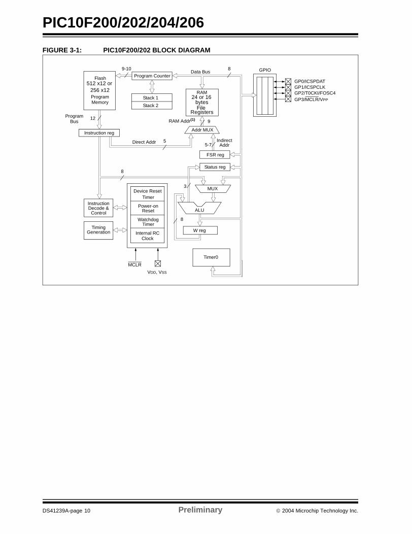
3.0 ARCHITECTURAL OVERVIEW
The high performance of the PIC10F200/202/204/206devices can be attributed to a number of architecturalfeatures commonly found in RISC microprocessors. Tobegin with, the PIC10F200/202/204/206 devices use aHarvard architecture in which program and data areaccessed on separate buses. This improves band-width over traditional von Neumann architectureswhere program and data are fetched on the same bus.Separating program and data memory further allowsinstructions to be sized differently than the 8-bit widedata word. Instruction opcodes are 12 bits wide,making it possible to have all single-word instructions.A 12-bit wide program memory access bus fetches a12-bit instruction in a single cycle. A two-stage pipelineoverlaps fetch and execution of instructions.Consequently, all instructions (33) execute in a singlecycle (1 µs @ 4 MHz) except for program branches.
The table below lists program memory (Flash) and datamemory (RAM) for the PIC10F200/202/204/206devices.
TABLE 3-1: PIC10F2XX MEMORY
The PIC10F200/202/204/206 devices can directly orindirectly address its register files and data memory. AllSpecial Function Registers (SFR), including the PC,are mapped in the data memory. The PIC10F200/202/204/206 devices have a highly orthogonal(symmetrical) instruction set that makes it possible tocarry out any operation, on any register, using anyaddressing mode. This symmetrical nature and lack of“special optimal situations” make programming with thePIC10F200/202/204/206 devices simple, yet efficient.In addition, the learning curve is reduced significantly.
The PIC10F200/202/204/206 devices contain an 8-bitALU and working register. The ALU is a generalpurpose arithmetic unit. It performs arithmetic andBoolean functions between data in the working registerand any register file.
The ALU is 8 bits wide and capable of addition, subtrac-tion, shift and logical operations. Unless otherwisementioned, arithmetic operations are two’s comple-ment in nature. In two-operand instructions, one oper-and is typically the W (working) register. The otheroperand is either a file register or an immediateconstant. In single operand instructions, the operand iseither the W register or a file register.
The W register is an 8-bit working register used for ALUoperations. It is not an addressable register.
Depending on the instruction executed, the ALU mayaffect the values of the Carry (C), Digit Carry (DC) andZero (Z) bits in the Status register. The C and DC bitsoperate as a borrow and digit borrow out bit, respec-tively, in subtraction. See the SUBWF and ADDWFinstructions for examples.
A simplified block diagram is shown in Figure 3-1 andFigure 3-2, with the corresponding device pinsdescribed in Table 3-2.
DeviceMemory
Program Data
PIC10F200 256 x 12 16 x 8
PIC10F202 512 x 12 24 x 8
PIC10F204 256 x 12 16 x 8
PIC10F206 512 x 12 24 x 8
2004 Microchip Technology Inc. Preliminary DS41239A-page 9
PIC10F200/202/204/206
FIGURE 3-1: PIC10F200/202 BLOCK DIAGRAM
Flash
ProgramMemory
9-10Data Bus
8
12ProgramBus
Instruction reg
Program Counter
RAM
FileRegisters
Direct Addr 5
RAM Addr(1) 9
Addr MUX
IndirectAddr
FSR reg
Status reg
MUX
ALU
W reg
Device Reset
Power-onReset
WatchdogTimer
InstructionDecode &
Control
TimingGeneration
MCLR
VDD, VSS
Timer0
GPIO
8
8
GP3/MCLR/VPP
GP2/T0CKI/FOSC4GP1/ICSPCLKGP0/ICSPDAT
5-7
3
Stack 1
Stack 2
24 or 16
Internal RC Clock
512 x12 or
bytes
Timer
256 x12
DS41239A-page 10 Preliminary 2004 Microchip Technology Inc.

PIC10F200/202/204/206
FIGURE 3-2: PIC10F204/206 BLOCK DIAGRAM
Flash
ProgramMemory
9-10Data Bus
8
12ProgramBus
Instruction reg
Program Counter
RAM
FileRegisters
Direct Addr 5
RAM Addr(1) 9
Addr MUX
IndirectAddr
FSR reg
Status reg
MUX
ALU
W reg
Device Reset
Power-onReset
WatchdogTimer
InstructionDecode &
Control
TimingGeneration
MCLR
VDD, VSS
Timer0
GPIO
8
8
GP3/MCLR/VPP
GP2/T0CKI/FOSC4GP1/ICSPCLKGP0/ICSPDAT
5-7
3
Stack 1
Stack 2
24 or 16
Internal RC Clock
512 x12 or
bytes
Timer
256 x12
ComparatorCIN+
CIN-
COUT
2004 Microchip Technology Inc. Preliminary DS41239A-page 11
PIC10F200/202/204/206
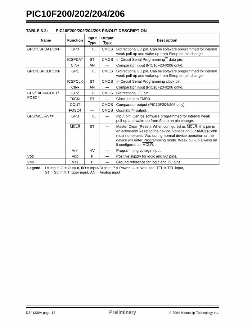
TABLE 3-2: PIC10F200/202/204/206 PINOUT DESCRIPTION
Name FunctionInput Type
Output Type
Description
GP0/ICSPDAT/CIN+ GP0 TTL CMOS Bidirectional I/O pin. Can be software programmed for internal weak pull-up and wake-up from Sleep on pin change.
ICSPDAT ST CMOS In-Circuit Serial Programming™ data pin.
CIN+ AN — Comparator input (PIC10F204/206 only).
GP1/ICSPCLK/CIN- GP1 TTL CMOS Bidirectional I/O pin. Can be software programmed for internal weak pull-up and wake-up from Sleep on pin change.
ICSPCLK ST CMOS In-Circuit Serial Programming clock pin.
CIN- AN — Comparator input (PIC10F204/206 only).
GP2/T0CKI/COUT/FOSC4
GP2 TTL CMOS Bidirectional I/O pin.
T0CKI ST — Clock input to TMR0.
COUT — CMOS Comparator output (PIC10F204/206 only).
FOSC4 — CMOS Oscillator/4 output.
GP3/MCLR/VPP GP3 TTL — Input pin. Can be software programmed for internal weak pull-up and wake-up from Sleep on pin change.
MCLR ST — Master Clear (Reset). When configured as MCLR, this pin is an active-low Reset to the device. Voltage on GP3/MCLR/VPP must not exceed VDD during normal device operation or the device will enter Programming mode. Weak pull-up always on if configured as MCLR.
VPP HV — Programming voltage input.
VDD VDD P — Positive supply for logic and I/O pins.
VSS VSS P — Ground reference for logic and I/O pins.
Legend: I = Input, O = Output, I/O = Input/Output, P = Power, — = Not used, TTL = TTL input,ST = Schmitt Trigger input, AN = Analog input
DS41239A-page 12 Preliminary 2004 Microchip Technology Inc.

PIC10F200/202/204/206
3.1 Clocking Scheme/Instruction Cycle
The clock is internally divided by four to generate fournon-overlapping quadrature clocks, namely Q1, Q2,Q3 and Q4. Internally, the PC is incremented every Q1and the instruction is fetched from program memoryand latched into the instruction register in Q4. It isdecoded and executed during the following Q1 throughQ4. The clocks and instruction execution flow is shownin Figure 3-3 and Example 3-1.
3.2 Instruction Flow/Pipelining
An instruction cycle consists of four Q cycles (Q1, Q2,Q3 and Q4). The instruction fetch and execute arepipelined such that fetch takes one instruction cycle,while decode and execute take another instructioncycle. However, due to the pipelining, each instructioneffectively executes in one cycle. If an instructioncauses the PC to change (e.g., GOTO), then two cyclesare required to complete the instruction (Example 3-1).
A fetch cycle begins with the PC incrementing in Q1.
In the execution cycle, the fetched instruction is latchedinto the Instruction Register (IR) in cycle Q1. Thisinstruction is then decoded and executed during theQ2, Q3 and Q4 cycles. Data memory is read during Q2(operand read) and written during Q4 (destinationwrite).
FIGURE 3-3: CLOCK/INSTRUCTION CYCLE
EXAMPLE 3-1: INSTRUCTION PIPELINE FLOW
Q1 Q2 Q3 Q4 Q1 Q2 Q3 Q4 Q1 Q2 Q3 Q4
OSC1
Q1
Q2
Q3
Q4
PC PC PC+1 PC+2
Fetch INST (PC)Execute INST (PC – 1) Fetch INST (PC + 1)
Execute INST (PC) Fetch INST (PC + 2)Execute INST (PC + 1)
Internalphaseclock
All instructions are single cycle, except for any program branches. These take two cycles, since the fetch instructionis “flushed” from the pipeline, while the new instruction is being fetched and then executed.
1. MOVLW 03H Fetch 1 Execute 1
2. MOVWF GPIO Fetch 2 Execute 2
3. CALL SUB_1 Fetch 3 Execute 3
4. BSF GPIO, BIT1 Fetch 4 Flush
Fetch SUB_1 Execute SUB_1
2004 Microchip Technology Inc. Preliminary DS41239A-page 13

PIC10F200/202/204/206
NOTES:
DS41239A-page 14 Preliminary 2004 Microchip Technology Inc.

PIC10F200/202/204/206
4.0 MEMORY ORGANIZATION
The PIC10F200/202/204/206 memories are organizedinto program memory and data memory. Data memorybanks are accessed using the File Select Register(FSR).
4.1 Program Memory Organization for the PIC10F200/204
The PIC10F200/204 devices have a 9-bit ProgramCounter (PC) capable of addressing a 512 x 12program memory space.
Only the first 256 x 12 (0000h-00FFh) for thePIC10F200/204 are physically implemented (seeFigure 4-1). Accessing a location above theseboundaries will cause a wraparound within the first256 x 12 space (PIC10F200/204). The effectiveReset vector is at 0000h (see Figure 4-1). Location00FFh (PIC10F200/204) contains the internal clockoscillator calibration value. This value should neverbe overwritten.
FIGURE 4-1: PROGRAM MEMORY MAP AND STACK FOR THE PIC10F200/204
CALL, RETLW
PC<7:0>
Stack Level 1Stack Level 2
Use
r M
emor
yS
pace
9
0000h
01FFh
On-chip ProgramMemory
Reset Vector(1)
Note 1: Address 0000h becomes theeffective Reset vector. Location 00FFh contains the MOVLW XX internal oscillator calibration value.
256 Word 00FFh0100h
2004 Microchip Technology Inc. Preliminary DS41239A-page 15

PIC10F200/202/204/206
4.2 Program Memory Organization for the PIC10F202/206
The PIC10F202/206 devices have a 10-bit ProgramCounter (PC) capable of addressing a 1024 x 12program memory space.
Only the first 512 x 12 (0000h-01FFh) for thePIC10F202/206 are physically implemented (seeFigure 4-2). Accessing a location above theseboundaries will cause a wraparound within the first512 x 12 space (PIC10F202/206). The effectiveReset vector is at 0000h (see Figure 4-2). Location01FFh (PIC10F202/206) contains the internal clockoscillator calibration value. This value should neverbe overwritten.
FIGURE 4-2: PROGRAM MEMORY MAP AND STACK FOR THE PIC10F202/206
4.3 Data Memory Organization
Data memory is composed of registers or bytes ofRAM. Therefore, data memory for a device is specifiedby its register file. The register file is divided into twofunctional groups: Special Function Registers (SFR)and General Purpose Registers (GPR).
The Special Function Registers include the TMR0 reg-ister, the Program Counter (PCL), the Status register,the I/O register (GPIO) and the File Select Register(FSR). In addition, Special Function Registers are usedto control the I/O port configuration and prescaleroptions.
The General Purpose Registers are used for data andcontrol information under command of the instructions.
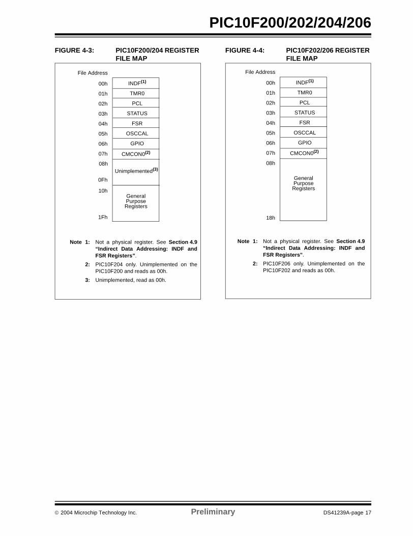
For the PIC10F200/204, the register file is composed of7 Special Function Registers and 16 General PurposeRegisters (see Figure 4-3 and Figure 4-4).
For the PIC10F202/206, the register file is composed of8 Special Function Registers and 24 General PurposeRegisters (see Figure 4-4).
4.3.1 GENERAL PURPOSE REGISTER FILE
The General Purpose Register file is accessed, eitherdirectly or indirectly, through the File Select Register(FSR). See Section 4.9 “Indirect Data Addressing:INDF and FSR Registers”.
CALL, RETLW
PC<8:0>
Stack Level 1Stack Level 2
Use
r M
emor
yS
pace
10
0000h
02FFh
Reset Vector(1)
Note 1: Address 0000h becomes theeffective Reset vector. Location 01FFh contains the MOVLW XX internal oscillator calibration value.
512 Words 01FFh0200h
On-chip ProgramMemory
DS41239A-page 16 Preliminary 2004 Microchip Technology Inc.
PIC10F200/202/204/206
FIGURE 4-3: PIC10F200/204 REGISTER FILE MAP
FIGURE 4-4: PIC10F202/206 REGISTER FILE MAP
File Address
00h
01h
02h
03h
04h
05h
06h
07h
10h
INDF(1)
TMR0
PCL
STATUS
FSR
OSCCAL
GPIO
GeneralPurposeRegisters
Note 1: Not a physical register. See Section 4.9“Indirect Data Addressing: INDF andFSR Registers”.
2: PIC10F204 only. Unimplemented on thePIC10F200 and reads as 00h.
3: Unimplemented, read as 00h.
08h
CMCON0(2)
0Fh
1Fh
Unimplemented(3)
File Address
00h
01h
02h
03h
04h
05h
06h
07h
18h
INDF(1)
TMR0
PCL
STATUS
FSR
OSCCAL
GPIO
GeneralPurposeRegisters
Note 1: Not a physical register. See Section 4.9“Indirect Data Addressing: INDF andFSR Registers”.
2: PIC10F206 only. Unimplemented on thePIC10F202 and reads as 00h.
08h
CMCON0(2)
2004 Microchip Technology Inc. Preliminary DS41239A-page 17

PIC10F200/202/204/206
4.3.2 SPECIAL FUNCTION REGISTERS
The Special Function Registers (SFRs) are registersused by the CPU and peripheral functions to control theoperation of the device (Table 4-1).
The Special Function Registers can be classified intotwo sets. The Special Function Registers associatedwith the “core” functions are described in this section.Those related to the operation of the peripheralfeatures are described in the section for eachperipheral feature.
TABLE 4-1: SPECIAL FUNCTION REGISTER (SFR) SUMMARY (PIC10F200/202/204/206)
Address Name Bit 7 Bit 6 Bit 5 Bit 4 Bit 3 Bit 2 Bit 1 Bit 0Value on
Power-OnReset(2)
Page #
00h INDF Uses Contents of FSR to Address Data Memory (not a physical register) xxxx xxxx 23
01h TMR0 8-bit Real-Time Clock/Counter xxxx xxxx 29, 33
02h(1) PCL Low-order 8 bits of PC 1111 1111 22
03h STATUS GPWUF CWUF(5) — TO PD Z DC C 00-1 1xxx(3) 19
04h FSR Indirect Data Memory Address Pointer 111x xxxx 23
05h OSCCAL CAL6 CAL5 CAL4 CAL3 CAL2 CAL1 CAL0 FOSC4 1111 1110 21
06h GPIO — — — — GP3 GP2 GP1 GP0 ---- xxxx 25
07h(4) CMCON0 CMPOUT COUTEN POL CMPT0CS CMPON CNREF CPREF CWU 1111 1111 34
N/A TRISGPIO — — — — I/O Control Register ---- 1111 37
N/A OPTION GPWU GPPU T0CS T0SE PSA PS2 PS1 PS0 1111 1111 20
Legend: — = unimplemented, read as ‘0’, x = unknown, u = unchanged, q = value depends on condition.Note 1: The upper byte of the Program Counter is not directly accessible. See Section 4.7 “Program Counter” for an
explanation of how to access these bits.2: Other (non Power-up) Resets include external Reset through MCLR, Watchdog Timer and wake-up on pin change
Reset.3: See Table 9-1 for other Reset specific values.4: PIC10F204/206 only.5: PIC10F204/206 only. On all other devices, this bit is reserved and should not be used.
DS41239A-page 18 Preliminary 2004 Microchip Technology Inc.
PIC10F200/202/204/206
4.4 Status Register
This register contains the arithmetic status of the ALU,the Reset status and the page preselect bit.
The Status register can be the destination for anyinstruction, as with any other register. If the Statusregister is the destination for an instruction that affectsthe Z, DC or C bits, then the write to these three bits isdisabled. These bits are set or cleared according to thedevice logic. Furthermore, the TO and PD bits are notwritable. Therefore, the result of an instruction with theStatus register as destination may be different thanintended.
For example, CLRF STATUS, will clear the upper threebits and set the Z bit. This leaves the Status register as000u u1uu (where u = unchanged).
Therefore, it is recommended that only BCF, BSF andMOVWF instructions be used to alter the Status register.These instructions do not affect the Z, DC or C bits fromthe Status register. For other instructions which doaffect Status bits, see Section 10.0 “Instruction SetSummary”.
REGISTER 4-1: STATUS REGISTER (ADDRESS: 03h) R/W-0 R/W-0 R/W-0 R-1 R-1 R/W-x R/W-x R/W-x
GPWUF CWUF(1) — TO PD Z DC C
bit 7 bit 0
bit 7 GPWUF: GPIO Reset bit 1 = Reset due to wake-up from Sleep on pin change0 = After power-up or other Reset
bit 6 CWUF: Comparator Wake-up on Change Flag Bit(1)
1 = Reset due to wake-up from Sleep on comparator change0 = After power-up or other Reset conditions.
bit 5 Reserved: Do not use. Use of this bit may affect upward compatibility with future products.
bit 4 TO: Time-out bit1 = After power-up, CLRWDT instruction or SLEEP instruction0 = A WDT time-out occurred
bit 3 PD: Power-down bit1 = After power-up or by the CLRWDT instruction0 = By execution of the SLEEP instruction
bit 2 Z: Zero bit1 = The result of an arithmetic or logic operation is zero0 = The result of an arithmetic or logic operation is not zero
bit 1 DC: Digit carry/borrow bit (for ADDWF and SUBWF instructions)ADDWF:1 = A carry from the 4th low-order bit of the result occurred0 = A carry from the 4th low-order bit of the result did not occurSUBWF:1 = A borrow from the 4th low-order bit of the result did not occur0 = A borrow from the 4th low-order bit of the result occurred
bit 0 C: Carry/borrow bit (for ADDWF, SUBWF and RRF, RLF instructions)ADDWF: SUBWF: RRF or RLF:1 = A carry occurred 1 = A borrow did not occur Load bit with LSb or MSb, respectively0 = A carry did not occur 0 = A borrow occurred
Note 1: This bit is used on the PIC10F204/206. For code compatibility do not use this bit onthe PIC10F200/202.
Legend:
R = Readable bit W = Writable bit U = Unimplemented bit, read as ‘0’
-n = Value at POR ‘1’ = Bit is set ‘0’ = Bit is cleared x = Bit is unknown
2004 Microchip Technology Inc. Preliminary DS41239A-page 19
PIC10F200/202/204/206
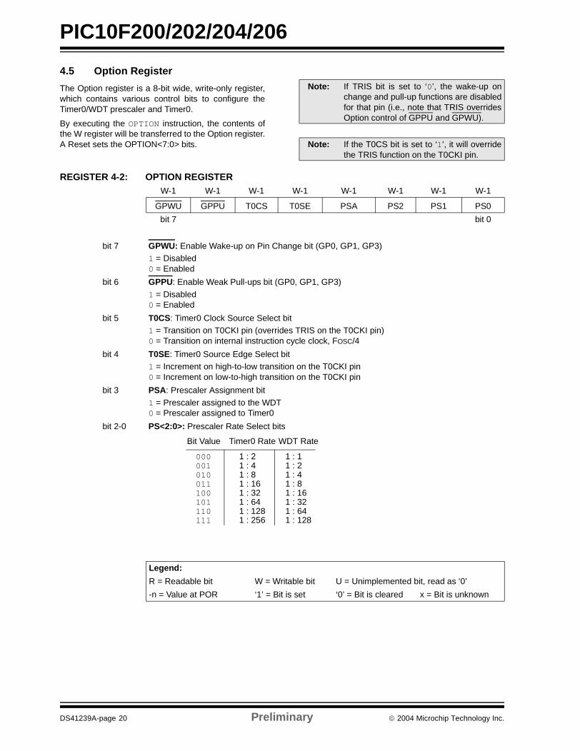
4.5 Option Register
The Option register is a 8-bit wide, write-only register,which contains various control bits to configure theTimer0/WDT prescaler and Timer0.
By executing the OPTION instruction, the contents ofthe W register will be transferred to the Option register.A Reset sets the OPTION<7:0> bits.
REGISTER 4-2: OPTION REGISTER
Note: If TRIS bit is set to ‘0’, the wake-up onchange and pull-up functions are disabledfor that pin (i.e., note that TRIS overridesOption control of GPPU and GPWU).
Note: If the T0CS bit is set to ‘1’, it will overridethe TRIS function on the T0CKI pin.
W-1 W-1 W-1 W-1 W-1 W-1 W-1 W-1
GPWU GPPU T0CS T0SE PSA PS2 PS1 PS0
bit 7 bit 0
bit 7 GPWU: Enable Wake-up on Pin Change bit (GP0, GP1, GP3)1 = Disabled0 = Enabled
bit 6 GPPU: Enable Weak Pull-ups bit (GP0, GP1, GP3)
1 = Disabled0 = Enabled
bit 5 T0CS: Timer0 Clock Source Select bit1 = Transition on T0CKI pin (overrides TRIS on the T0CKI pin)0 = Transition on internal instruction cycle clock, FOSC/4
bit 4 T0SE: Timer0 Source Edge Select bit1 = Increment on high-to-low transition on the T0CKI pin0 = Increment on low-to-high transition on the T0CKI pin
bit 3 PSA: Prescaler Assignment bit
1 = Prescaler assigned to the WDT0 = Prescaler assigned to Timer0
bit 2-0 PS<2:0>: Prescaler Rate Select bits
Legend:
R = Readable bit W = Writable bit U = Unimplemented bit, read as ‘0’
-n = Value at POR ‘1’ = Bit is set ‘0’ = Bit is cleared x = Bit is unknown
000001010011100101110111
1 : 21 : 41 : 81 : 161 : 321 : 641 : 1281 : 256
1 : 11 : 21 : 41 : 81 : 161 : 321 : 641 : 128
Bit Value Timer0 Rate WDT Rate
DS41239A-page 20 Preliminary 2004 Microchip Technology Inc.

PIC10F200/202/204/206
4.6 OSCCAL Register
The Oscillator Calibration (OSCCAL) register is used tocalibrate the internal precision 4 MHz oscillator. Itcontains seven bits for calibration.
After you move in the calibration constant, do notchange the value. See Section 9.2.2 “Internal 4 MHzOscillator”.
REGISTER 4-3: OSCCAL REGISTER (ADDRESS: 05h)
Note: Erasing the device will also erase the pre-programmed internal calibration value forthe internal oscillator. The calibrationvalue must be read prior to erasing thepart so it can be reprogrammed correctlylater.
R/W-1 R/W-1 R/W-1 R/W-1 R/W-1 R/W-1 R/W-1 R/W-0
CAL6 CAL5 CAL4 CAL3 CAL2 CAL1 CAL0 FOSC4
bit 7 bit 0
bit 7-1 CAL<6:0>: Oscillator Calibration bits0111111 = Maximum frequency•••0000001 0000000 = Center frequency1111111•••1000000 = Minimum frequency
bit 0 FOSC4: INTOSC/4 Output Enable bit(1) 1 = INTOSC/4 output onto GP20 = GP2/T0CKI/COUT applied to GP2
Note 1: Overrides GP2/T0CKI/COUT control registers when enabled.
Legend:
R = Readable bit W = Writable bit U = Unimplemented bit, read as ‘0’
-n = Value at POR ‘1’ = Bit is set ‘0’ = Bit is cleared x = Bit is unknown
2004 Microchip Technology Inc. Preliminary DS41239A-page 21

PIC10F200/202/204/206
4.7 Program Counter
As a program instruction is executed, the ProgramCounter (PC) will contain the address of the nextprogram instruction to be executed. The PC value isincreased by one every instruction cycle, unless aninstruction changes the PC.
For a GOTO instruction, bits 8:0 of the PC are providedby the GOTO instruction word. The Program Counter(PCL) is mapped to PC<7:0>.
For a CALL instruction, or any instruction where thePCL is the destination, bits 7:0 of the PC again are pro-vided by the instruction word. However, PC<8> doesnot come from the instruction word, but is alwayscleared (Figure 4-5).
Instructions where the PCL is the destination, or modifyPCL instructions, include MOVWF PC, ADDWF PC andBSF PC,5.
FIGURE 4-5: LOADING OF PCBRANCH INSTRUCTIONS
4.7.1 EFFECTS OF RESET
The PC is set upon a Reset, which means that the PCaddresses the last location in program memory (i.e.,the oscillator calibration instruction). After executingMOVLW XX, the PC will roll over to location 0000h andbegin executing user code.
4.8 Stack
The PIC10F200/204 devices have a 2-deep, 8-bit widehardware PUSH/POP stack.
The PIC10F202/206 devices have a 2-deep, 9-bit widehardware PUSH/POP stack.
A CALL instruction will PUSH the current value of Stack 1into Stack 2 and then PUSH the current PC value,incremented by one, into Stack Level 1. If more than twosequential CALLs are executed, only the most recent tworeturn addresses are stored.
A RETLW instruction will POP the contents of StackLevel 1 into the PC and then copy Stack Level 2contents into level 1. If more than two sequentialRETLWs are executed, the stack will be filled with theaddress previously stored in Stack Level 2. Note thatthe W register will be loaded with the literal valuespecified in the instruction. This is particularly useful forthe implementation of data look-up tables within theprogram memory.
Note: Because PC<8> is cleared in the CALLinstruction or any modify PCL instruction,all subroutine calls or computed jumps arelimited to the first 256 locations of anyprogram memory page (512 words long).
PC8 7 0
PCL
Instruction Word
GOTO Instruction
CALL or Modify PCL Instruction
PC8 7 0
PCL
Instruction Word
Reset to ‘0’
Note 1: There are no Status bits to indicate stackoverflows or stack underflow conditions.
2: There are no instruction mnemonicscalled PUSH or POP. These are actionsthat occur from the execution of the CALLand RETLW instructions.
DS41239A-page 22 Preliminary 2004 Microchip Technology Inc.
PIC10F200/202/204/206
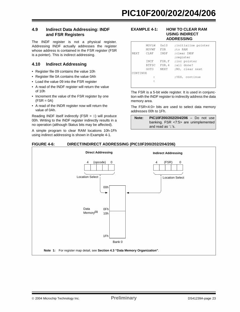
4.9 Indirect Data Addressing: INDF and FSR Registers
The INDF register is not a physical register.Addressing INDF actually addresses the registerwhose address is contained in the FSR register (FSRis a pointer). This is indirect addressing.
4.10 Indirect Addressing
• Register file 09 contains the value 10h• Register file 0A contains the value 0Ah• Load the value 09 into the FSR register
• A read of the INDF register will return the value of 10h
• Increment the value of the FSR register by one (FSR = 0A)
• A read of the INDR register now will return the value of 0Ah.
Reading INDF itself indirectly (FSR = 0) will produce00h. Writing to the INDF register indirectly results in ano operation (although Status bits may be affected).
A simple program to clear RAM locations 10h-1Fhusing indirect addressing is shown in Example 4-1.
EXAMPLE 4-1: HOW TO CLEAR RAM USING INDIRECT ADDRESSING
The FSR is a 5-bit wide register. It is used in conjunc-tion with the INDF register to indirectly address the datamemory area.
The FSR<4:0> bits are used to select data memoryaddresses 00h to 1Fh.
FIGURE 4-6: DIRECT/INDIRECT ADDRESSING (PIC10F200/202/204/206)
Note: PIC10F200/202/204/206 – Do not usebanking. FSR <7:5> are unimplementedand read as ‘1’s.
MOVLW 0x10 ;initialize pointerMOVWF FSR ;to RAM
NEXT CLRF INDF ;clear INDF ;register
INCF FSR,F ;inc pointerBTFSC FSR,4 ;all done?GOTO NEXT ;NO, clear next
CONTINUE: ;YES, continue:
Note 1: For register map detail, see Section 4.3 “Data Memory Organization”.
Location SelectLocation Select
Indirect AddressingDirect Addressing
Data Memory(1)
0Fh10h
Bank 0
04 (FSR)
00h
1Fh
(opcode) 04
2004 Microchip Technology Inc. Preliminary DS41239A-page 23

PIC10F200/202/204/206
NOTES:
DS41239A-page 24 Preliminary 2004 Microchip Technology Inc.

PIC10F200/202/204/206
5.0 I/O PORT
As with any other register, the I/O register(s) can bewritten and read under program control. However, readinstructions (e.g., MOVF GPIO, W) always read the I/Opins independent of the pin’s Input/Output modes. OnReset, all I/O ports are defined as input (inputs are athigh-impedance) since the I/O control registers are allset.
5.1 GPIO
GPIO is an 8-bit I/O register. Only the low-order 4 bitsare used (GP<3:0>). Bits 7 through 4 are unimple-mented and read as ‘0’s. Please note that GP3 is aninput only pin. Pins GP0, GP1 and GP3 can be config-ured with weak pull-ups and also for wake-up onchange. The wake-up on change and weak pull-upfunctions are not pin selectable. If GP3/MCLR is config-ured as MCLR, weak pull-up is always on and wake-upon change for this pin is not enabled.
5.2 TRIS Registers
The Output Driver Control register is loaded with thecontents of the W register by executing the TRIS finstruction. A ‘1’ from a TRIS register bit puts the corre-sponding output driver in a High-impedance mode. A‘0’ puts the contents of the output data latch on theselected pins, enabling the output buffer. The excep-tions are GP3, which is input only and the GP2/T0CKI/COUT/FOSC4 pin, which may be controlled by variousregisters. See Table 5-1.
The TRIS registers are “write-only” and are set (outputdrivers disabled) upon Reset.
TABLE 5-1: ORDER OF PRECEDENCE FOR PIN FUNCTIONS
5.3 I/O Interfacing
The equivalent circuit for an I/O port pin is shown inFigure 5-2. All port pins, except GP3 which is inputonly, may be used for both input and output operations.For input operations, these ports are non-latching. Anyinput must be present until read by an input instruction(e.g., MOVF GPIO, W). The outputs are latched andremain unchanged until the output latch is rewritten. Touse a port pin as output, the corresponding directioncontrol bit in TRIS must be cleared (= 0). For use as aninput, the corresponding TRIS bit must be set. Any I/Opin (except GP3) can be programmed individually asinput or output.
FIGURE 5-1: PIC10F200/202/204/206 EQUIVALENT CIRCUIT FOR A SINGLE I/O PIN
Note: A read of the ports reads the pins, not theoutput data latches. That is, if an outputdriver on a pin is enabled and driven high,but the external system is holding it low, aread of the port will indicate that the pin islow.
Priority GP0 GP1 GP2 GP3
1 CIN+ CIN- FOSC4 I/MCLR
2 TRIS GPIO TRIS GPIO COUT —
3 — — T0CKI —
4 — — TRIS GPIO —
DataBus
QD
QCK
QD
QCKP
N
WRPort
TRIS ‘f’
Data
TRIS
RD Port
VSS
VDD
I/Opin
WReg
Latch
Latch
Reset
Note 1: See Table 3-2 for buffer type.
VSS
VDD
(1)
2004 Microchip Technology Inc. Preliminary DS41239A-page 25

PIC10F200/202/204/206
TABLE 5-2: SUMMARY OF PORT REGISTERS
5.4 I/O Programming Considerations
5.4.1 BIDIRECTIONAL I/O PORTS
Some instructions operate internally as read followedby write operations. The BCF and BSF instructions, forexample, read the entire port into the CPU, execute thebit operation and rewrite the result. Caution must beused when these instructions are applied to a portwhere one or more pins are used as input/outputs. Forexample, a BSF operation on bit 2 of GPIO will causeall eight bits of GPIO to be read into the CPU, bit 2 tobe set and the GPIO value to be written to the outputlatches. If another bit of GPIO is used as a bidirectionalI/O pin (say bit 0) and it is defined as an input at thistime, the input signal present on the pin itself would beread into the CPU and rewritten to the data latch of thisparticular pin, overwriting the previous content. As longas the pin stays in the Input mode, no problem occurs.However, if bit 0 is switched into Output mode later on,the content of the data latch may now be unknown.
Example 5-1 shows the effect of two sequentialRead-Modify-Write instructions (e.g., BCF, BSF, etc.)on an I/O port.
A pin actively outputting a high or a low should not bedriven from external devices at the same time in orderto change the level on this pin (“wired OR”, “wiredAND”). The resulting high output currents may damagethe chip.
EXAMPLE 5-1: READ-MODIFY-WRITE INSTRUCTIONS ON AN I/O PORT
5.4.2 SUCCESSIVE OPERATIONS ONI/O PORTS
The actual write to an I/O port happens at the end of aninstruction cycle, whereas for reading, the data must bevalid at the beginning of the instruction cycle (Figure 5-2).Therefore, care must be exercised if a write followed bya read operation is carried out on the same I/O port. Thesequence of instructions should allow the pin voltage tostabilize (load dependent) before the next instructioncauses that file to be read into the CPU. Otherwise, theprevious state of that pin may be read into the CPU ratherthan the new state. When in doubt, it is better to separatethese instructions with a NOP or another instruction notaccessing this I/O port.
Address Name Bit 7 Bit 6 Bit 5 Bit 4 Bit 3 Bit 2 Bit 1 Bit 0Value on
Power-OnReset
Value onAll Other Resets
N/A TRISGPIO — — — — I/O Control Register ---- 1111 ---- 1111
N/A OPTION GPWU GPPU T0CS T0SE PSA PS2 PS1 PS0 1111 1111 1111 1111
03h STATUS GPWUF CWUF — TO PD Z DC C 00-1 1xxx qq-q quuu(1, 2)
06h GPIO — — — — GP3 GP2 GP1 GP0 ---- xxxx ---- uuuu
Legend: Shaded cells are not used by Port registers, read as ‘0’, — = unimplemented, read as ‘0’, x = unknown, u = unchanged, q = depends on condition.
Note 1: If Reset was due to wake-up on pin change, then bit 7 = 1. All other Resets will cause bit 7 = 0.2: If Reset was due to wake-up on comparator change, then bit 6 = 1. All other Resets will cause bit 6 = 0.
;Initial GPIO Settings;GPIO<3:2> Inputs;GPIO<1:0> Outputs;; GPIO latch GPIO pins; ---------- ----------BCF GPIO, 1 ;---- pp01 ---- pp11BCF GPIO, 0 ;---- pp10 ---- pp11MOVLW 007h;TRIS GPIO ;---- pp10 ---- pp11
;
Note 1: The user may have expected the pin values to be ---- pp00. The 2nd BCF caused GP1 to be latched as the pin value (High).
DS41239A-page 26 Preliminary 2004 Microchip Technology Inc.

PIC10F200/202/204/206
FIGURE 5-2: SUCCESSIVE I/O OPERATION (PIC10F200/202/204/206)
PC PC + 1 PC + 2 PC + 3
Q1 Q2 Q3 Q4 Q1 Q2 Q3 Q4 Q1 Q2 Q3 Q4 Q1 Q2 Q3 Q4
InstructionFetched
GP<2:0>
MOVWF GPIO NOP
Port pinsampled here
NOPMOVF GPIO, W
InstructionExecuted MOVWF GPIO
(Write to GPIO)NOPMOVF GPIO,W
This example shows a write to GPIO followedby a read from GPIO.
Data setup time = (0.25 TCY – TPD)
where: TCY = instruction cycle.
TPD = propagation delay
Therefore, at higher clock frequencies, awrite followed by a read may be problematic.
(Read GPIO)
Port pinwritten here
2004 Microchip Technology Inc. Preliminary DS41239A-page 27

PIC10F200/202/204/206
NOTES:
DS41239A-page 28 Preliminary 2004 Microchip Technology Inc.

PIC10F200/202/204/206
6.0 TIMER0 MODULE AND TMR0 REGISTER (PIC10F200/202)
The Timer0 module has the following features:
• 8-bit timer/counter register, TMR0
• Readable and writable• 8-bit software programmable prescaler• Internal or external clock select:
- Edge select for external clock
Figure 6-1 is a simplified block diagram of the Timer0module.
Timer mode is selected by clearing the T0CS bit(Option<5>). In Timer mode, the Timer0 module willincrement every instruction cycle (without prescaler). IfTMR0 register is written, the increment is inhibited forthe following two cycles (Figure 6-2 and Figure 6-3).The user can work around this by writing an adjustedvalue to the TMR0 register.
Counter mode is selected by setting the T0CS bit(Option<5>). In this mode, Timer0 will increment eitheron every rising or falling edge of pin T0CKI. The T0SEbit (Option<4>) determines the source edge. Clearingthe T0SE bit selects the rising edge. Restrictions on theexternal clock input are discussed in detail inSection 6.1 “Using Timer0 with an External Clock(PIC10F200/202)”.
The prescaler may be used by either the Timer0module or the Watchdog Timer, but not both. Theprescaler assignment is controlled in software by thecontrol bit, PSA (Option<3>). Clearing the PSA bit willassign the prescaler to Timer0. The prescaler is notreadable or writable. When the prescaler is assigned tothe Timer0 module, prescale values of 1:2, 1:4, 1:256are selectable. Section 6.2 “Prescaler” details theoperation of the prescaler.
A summary of registers associated with the Timer0module is found in Table 6-1.
FIGURE 6-1: TIMER0 BLOCK DIAGRAM
FIGURE 6-2: TIMER0 TIMING: INTERNAL CLOCK/NO PRESCALE
Note 1: Bits T0CS, T0SE, PSA, PS2, PS1 and PS0 are located in the Option register.
2: The prescaler is shared with the Watchdog Timer (Figure 6-5).
0
1
1
0
T0CS(1)
FOSC/4
ProgrammablePrescaler(2)
Sync withInternalClocks
TMR0 reg
PSOUT
(2 TCY delay)
PSOUT
Data Bus
8
PSA(1)PS2, PS1, PS0(1)3
SyncT0SE
GP2/T0CKIPin
PC – 1
Q1 Q2 Q3 Q4 Q1 Q2 Q3 Q4 Q1 Q2 Q3 Q4 Q1 Q2 Q3 Q4 Q1 Q2 Q3 Q4 Q1 Q2 Q3 Q4 Q1 Q2 Q3 Q4 Q1 Q2 Q3 Q4
InstructionFetch
Timer0
PC PC + 1 PC + 2 PC + 3 PC + 4 PC + 6
T0 T0 + 1 T0 + 2 NT0 NT0 + 1 NT0 + 2
MOVWF TMR0 MOVF TMR0,W MOVF TMR0,W MOVF TMR0,W MOVF TMR0,W MOVF TMR0,W
Write TMR0executed
Read TMR0reads NT0
Read TMR0reads NT0
Read TMR0reads NT0
Read TMR0reads NT0 + 1
Read TMR0reads NT0 + 2
InstructionExecuted
PC + 5
PC(ProgramCounter)
2004 Microchip Technology Inc. Preliminary DS41239A-page 29

PIC10F200/202/204/206
FIGURE 6-3: TIMER0 TIMING: INTERNAL CLOCK/PRESCALE 1:2
TABLE 6-1: REGISTERS ASSOCIATED WITH TIMER0
6.1 Using Timer0 with an External Clock (PIC10F200/202)
When an external clock input is used for Timer0, it mustmeet certain requirements. The external clock require-ment is due to internal phase clock (TOSC) synchroniza-tion. Also, there is a delay in the actual incrementing ofTimer0 after synchronization.
6.1.1 EXTERNAL CLOCK SYNCHRONIZATION
When no prescaler is used, the external clock input isthe same as the prescaler output. The synchronizationof T0CKI with the internal phase clocks is accom-plished by sampling the prescaler output on the Q2 andQ4 cycles of the internal phase clocks (Figure 6-4).Therefore, it is necessary for T0CKI to be high for atleast 2 TOSC (and a small RC delay of 2 Tt0H) and lowfor at least 2 TOSC (and a small RC delay of 2 Tt0H).Refer to the electrical specification of the desireddevice.
When a prescaler is used, the external clock input isdivided by the asynchronous ripple counter-typeprescaler, so that the prescaler output is symmetrical.For the external clock to meet the sampling require-ment, the ripple counter must be taken into account.Therefore, it is necessary for T0CKI to have a period ofat least 4 TOSC (and a small RC delay of 4 Tt0H) dividedby the prescaler value. The only requirement on T0CKIhigh and low time is that they do not violate theminimum pulse width requirement of Tt0H. Refer toparameters 40, 41 and 42 in the electrical specificationof the desired device.
Address Name Bit 7 Bit 6 Bit 5 Bit 4 Bit 3 Bit 2 Bit 1 Bit 0Value on
Power-OnReset
Value onAll Other Resets
01h TMR0 Timer0 – 8-bit Real-Time Clock/Counter xxxx xxxx uuuu uuuu
N/A OPTION GPWU GPPU T0CS T0SE PSA PS2 PS1 PS0 1111 1111 1111 1111
N/A TRISGPIO(1) — — — — I/O Control Register ---- 1111 ---- 1111
Legend: Shaded cells not used by Timer0. — = unimplemented, x = unknown, u = unchanged.
Note 1: The TRIS of the T0CKI pin is overridden when T0CS = 1.
PC – 1
Q1 Q2 Q3 Q4 Q1 Q2 Q3 Q4 Q1 Q2 Q3 Q4 Q1 Q2 Q3 Q4 Q1 Q2 Q3 Q4 Q1 Q2 Q3 Q4 Q1 Q2 Q3 Q4 Q1 Q2 Q3 Q4
InstructionFetch
Timer0
PC PC + 1 PC + 2 PC + 3 PC + 4 PC + 6
T0 T0 + 1 NT0 NT0 + 1
MOVWF TMR0 MOVF TMR0,W MOVF TMR0,W MOVF TMR0,W MOVF TMR0,W MOVF TMR0,W
Write TMR0executed
Read TMR0reads NT0
Read TMR0reads NT0
Read TMR0reads NT0
Read TMR0reads NT0 + 1
Read TMR0reads NT0 + 2
InstructionExecuted
PC + 5
PC(ProgramCounter)
DS41239A-page 30 Preliminary 2004 Microchip Technology Inc.

PIC10F200/202/204/206
6.1.2 TIMER0 INCREMENT DELAY
Since the prescaler output is synchronized with theinternal clocks, there is a small delay from the time theexternal clock edge occurs to the time the Timer0module is actually incremented. Figure 6-4 shows thedelay from the external clock edge to the timerincrementing.
FIGURE 6-4: TIMER0 TIMING WITH EXTERNAL CLOCK
6.2 Prescaler
An 8-bit counter is available as a prescaler for theTimer0 module or as a postscaler for the WatchdogTimer (WDT), respectively (see Section 9.6 “Watch-dog Timer (WDT)”). For simplicity, this counter isbeing referred to as “prescaler” throughout this datasheet.
The PSA and PS<2:0> bits (Option<3:0>) determineprescaler assignment and prescale ratio.
When assigned to the Timer0 module, all instructionswriting to the TMR0 register (e.g., CLRF 1, MOVWF 1,BSF 1,x, etc.) will clear the prescaler. When assignedto WDT, a CLRWDT instruction will clear the prescaleralong with the WDT. The prescaler is neither readablenor writable. On a Reset, the prescaler contains all ‘0’s.
6.2.1 SWITCHING PRESCALER ASSIGNMENT
The prescaler assignment is fully under softwarecontrol (i.e., it can be changed “on-the-fly” during pro-gram execution). To avoid an unintended device Reset,the following instruction sequence (Example 6-1) mustbe executed when changing the prescaler assignmentfrom Timer0 to the WDT.
EXAMPLE 6-1: CHANGING PRESCALER (TIMER0 → WDT)
Increment Timer0 (Q4)
External Clock Input or
Q1 Q2 Q3 Q4 Q1 Q2 Q3 Q4 Q1 Q2 Q3 Q4 Q1 Q2 Q3 Q4
Timer0 T0 T0 + 1 T0 + 2
Small pulse misses sampling
External Clock/PrescalerOutput After Sampling
(3)
Prescaler Output (2)
(1)
Note 1: Delay from clock input change to Timer0 increment is 3 TOSC to 7 TOSC (Duration of Q = TOSC). Therefore, the errorin measuring the interval between two edges on Timer0 input = ±4 TOSC max.
2: External clock if no prescaler selected; prescaler output otherwise.
3: The arrows indicate the points in time where sampling occurs.
Note: The prescaler may be used by either theTimer0 module or the WDT, but not both.Thus, a prescaler assignment for theTimer0 module means that there is noprescaler for the WDT and vice versa. CLRWDT ;Clear WDT
CLRF TMR0 ;Clear TMR0 & Prescaler MOVLW ‘00xx1111’b ;These 3 lines (5, 6, 7)OPTION ;are required only if
;desiredCLRWDT ;PS<2:0> are 000 or 001MOVLW ‘00xx1xxx’b ;Set Postscaler toOPTION ;desired WDT rate
2004 Microchip Technology Inc. Preliminary DS41239A-page 31

PIC10F200/202/204/206
To change the prescaler from the WDT to the Timer0module, use the sequence shown in Example 6-2. Thissequence must be used even if the WDT is disabled. ACLRWDT instruction should be executed beforeswitching the prescaler.
EXAMPLE 6-2: CHANGING PRESCALER (WDT→TIMER0)
FIGURE 6-5: BLOCK DIAGRAM OF THE TIMER0/WDT PRESCALER
CLRWDT ;Clear WDT and ;prescaler
MOVLW ‘xxxx0xxx’ ;Select TMR0, new ;prescale value and;clock source
OPTION
TCY (= FOSC/4)
Sync2
CyclesTMR0 reg
8-bit Prescaler
8-to-1MUX
M
MUX
WatchdogTimer
PSA(1)
0 1
0
1
WDTTime-Out
PS<2:0>(1)
8
PSA(1)WDT Enable bit
0
10
1
Data Bus
8
PSA(1)T0CS(1)
MUX M
UX
UX
T0SE(1)
GP2/T0CKI(2)
Pin
Note 1: T0CS, T0SE, PSA, PS<2:0> are bits in the Option register.
2: T0CKI is shared with pin GP2 on the PIC10F200/202/204/206.
DS41239A-page 32 Preliminary 2004 Microchip Technology Inc.

PIC10F200/202/204/206
7.0 TIMER0 MODULE AND TMR0 REGISTER (PIC10F204/206)
The Timer0 module has the following features:
• 8-bit timer/counter register, TMR0
• Readable and writable• 8-bit software programmable prescaler• Internal or external clock select:
- Edge select for external clock- External clock from either the T0CKI pin or
from the output of the comparator
Figure 7-1 is a simplified block diagram of the Timer0module.
Timer mode is selected by clearing the T0CS bit(Option<5>). In Timer mode, the Timer0 module willincrement every instruction cycle (without prescaler). IfTMR0 register is written, the increment is inhibited forthe following two cycles (Figure 7-2 and Figure 7-3).The user can work around this by writing an adjustedvalue to the TMR0 register.
There are two types of Counter mode. The first Countermode uses the T0CKI pin to increment Timer0. It isselected by setting the T0CS bit (Option<5>), settingthe CMPT0CS bit (CMCON0<4>) and setting theCOUTEN bit (CMCON0<6>). In this mode, Timer0 willincrement either on every rising or falling edge of pinT0CKI. The T0SE bit (Option<4>) determines thesource edge. Clearing the T0SE bit selects the risingedge. Restrictions on the external clock input arediscussed in detail in Section 7.1 “Using Timer0 withan External Clock (PIC10F204/206)”.
The second Counter mode uses the output of the com-parator to increment Timer0. It can be entered in twodifferent ways. The first way is selected by setting theT0CS bit (Option<5>) and clearing the CMPT0CS bit(CMCON<4>); (COUTEN ([CMCON<6>]) does notaffect this mode of operation. This enables an internalconnection between the comparator and the Timer0.
The second way is selected by setting the T0CS bit(Option<5>), setting the CMPT0CS bit (CMCON0<4>)and clearing the COUTEN bit (CMCON0<6>). Thisallows the output of the comparator onto the T0CKI pin,while keeping the T0CKI input active. Therefore, anycomparator change on the COUT pin is fed back intothe T0CKI input. The T0SE bit (Option<4>) determinesthe source edge. Clearing the T0SE bit selects therising edge. Restrictions on the external clock input asdiscussed in Section 7.1 “Using Timer0 with anExternal Clock (PIC10F204/206)”
The prescaler may be used by either the Timer0module or the Watchdog Timer, but not both. Theprescaler assignment is controlled in software by thecontrol bit, PSA (Option<3>). Clearing the PSA bit willassign the prescaler to Timer0. The prescaler is notreadable or writable. When the prescaler is assigned tothe Timer0 module, prescale values of 1:2, 1:4,...,1:256 are selectable. Section 7.2 “Prescaler” detailsthe operation of the prescaler.
A summary of registers associated with the Timer0module is found in Table 7-1.
FIGURE 7-1: TIMER0 BLOCK DIAGRAM (PIC10F204/206)
Note 1: Bits T0CS, T0SE, PSA, PS2, PS1 and PS0 are located in the Option register.2: The prescaler is shared with the Watchdog Timer (Figure 7-5).3: Bit CMPT0CS is located in the CMCON0 register, CMCON0<4>.
0
1
1
0
T0CS(1)
FOSC/4
ProgrammablePrescaler(2)
Sync withInternalClocks
TMR0 reg
PSOUT
(2 TCY delay)
PSOUT
Data Bus
8
PSA(1)PS2, PS1, PS0(1)3
SyncT0SE(1)
T0CKIPin
CMPT0CS(3)
1
0
InternalComparator Output
2004 Microchip Technology Inc. Preliminary DS41239A-page 33

PIC10F200/202/204/206
FIGURE 7-2: TIMER0 TIMING: INTERNAL CLOCK/NO PRESCALE
FIGURE 7-3: TIMER0 TIMING: INTERNAL CLOCK/PRESCALE 1:2
TABLE 7-1: REGISTERS ASSOCIATED WITH TIMER0
7.1 Using Timer0 with an External Clock (PIC10F204/206)
When an external clock input is used for Timer0, it mustmeet certain requirements. The external clock require-ment is due to internal phase clock (TOSC) synchroniza-tion. Also, there is a delay in the actual incrementing ofTimer0 after synchronization.
7.1.1 EXTERNAL CLOCK SYNCHRONIZATION
When no prescaler is used, the external clock input isthe same as the prescaler output. The synchronizationof an external clock with the internal phase clocks isaccomplished by sampling the prescaler output on theQ2 and Q4 cycles of the internal phase clocks(Figure 7-4). Therefore, it is necessary for T0CKI or thecomparator output to be high for at least 2 TOSC (and a
small RC delay of 2 Tt0H) and low for at least 2 TOSC
(and a small RC delay of 2 Tt0H). Refer to the electricalspecification of the desired device.
When a prescaler is used, the external clock input isdivided by the asynchronous ripple counter typeprescaler, so that the prescaler output is symmetrical.For the external clock to meet the sampling require-ment, the ripple counter must be taken into account.Therefore, it is necessary for T0CKI or the comparatoroutput to have a period of at least 4 TOSC (and a smallRC delay of 4 Tt0H) divided by the prescaler value. Theonly requirement on T0CKI or the comparator outputhigh and low time is that they do not violate theminimum pulse width requirement of Tt0H. Refer toparameters 40, 41 and 42 in the electrical specificationof the desired device.
Address Name Bit 7 Bit 6 Bit 5 Bit 4 Bit 3 Bit 2 Bit 1 Bit 0Value on
Power-OnReset
Value onAll Other Resets
01h TMR0 Timer0 – 8-bit Real-Time Clock/Counter xxxx xxxx uuuu uuuu
07h CMCON0 CMPOUT COUTEN POL CMPT0CS CMPON CNREF CPREF CWU 1111 1111 uuuu uuuu
N/A OPTION GPWU GPPU T0CS T0SE PSA PS2 PS1 PS0 1111 1111 1111 1111
N/A TRISGPIO(1) — — — — I/O Control Register ---- 1111 ---- 1111
Legend: Shaded cells not used by Timer0. — = unimplemented, x = unknown, u = unchanged.Note 1: The TRIS of the T0CKI pin is overridden when T0CS = 1.
PC – 1
Q1 Q2 Q3 Q4 Q1 Q2 Q3 Q4 Q1 Q2 Q3 Q4 Q1 Q2 Q3 Q4 Q1 Q2 Q3 Q4 Q1 Q2 Q3 Q4 Q1 Q2 Q3 Q4 Q1 Q2 Q3 Q4
InstructionFetch
Timer0
PC PC + 1 PC + 2 PC + 3 PC + 4 PC + 6
T0 T0 + 1 T0 + 2 NT0 NT0 + 1 NT0 + 2
MOVWF TMR0 MOVF TMR0,W MOVF TMR0,W MOVF TMR0,W MOVF TMR0,W MOVF TMR0,W
Write TMR0executed
Read TMR0reads NT0
Read TMR0reads NT0
Read TMR0reads NT0
Read TMR0reads NT0 + 1
Read TMR0reads NT0 + 2
InstructionExecuted
PC+5
PC(ProgramCounter)
PC – 1
Q1 Q2 Q3 Q4 Q1 Q2 Q3 Q4 Q1 Q2 Q3 Q4 Q1 Q2 Q3 Q4 Q1 Q2 Q3 Q4 Q1 Q2 Q3 Q4 Q1 Q2 Q3 Q4 Q1 Q2 Q3 Q4
InstructionFetch
Timer0
PC PC + 1 PC + 2 PC + 3 PC + 4 PC + 6
T0 T0 + 1 NT0 NT0 + 1
MOVWF TMR0 MOVF TMR0,W MOVF TMR0,W MOVF TMR0,W MOVF TMR0,W MOVF TMR0,W
Write TMR0executed
Read TMR0reads NT0
Read TMR0reads NT0
Read TMR0reads NT0
Read TMR0reads NT0 + 1
Read TMR0reads NT0 + 2
InstructionExecuted
PC + 5
PC(ProgramCounter)
DS41239A-page 34 Preliminary 2004 Microchip Technology Inc.

PIC10F200/202/204/206
7.1.2 TIMER0 INCREMENT DELAY
Since the prescaler output is synchronized with theinternal clocks, there is a small delay from the time theexternal clock edge occurs to the time the Timer0module is actually incremented. Figure 7-4 shows thedelay from the external clock edge to the timerincrementing.
FIGURE 7-4: TIMER0 TIMING WITH EXTERNAL CLOCK
7.2 Prescaler
An 8-bit counter is available as a prescaler for theTimer0 module or as a postscaler for the WatchdogTimer (WDT), respectively (see Figure 9-6). Forsimplicity, this counter is being referred to as“prescaler” throughout this data sheet.
The PSA and PS<2:0> bits (Option<3:0>) determineprescaler assignment and prescale ratio.
When assigned to the Timer0 module, all instructionswriting to the TMR0 register (e.g., CLRF 1, MOVWF 1,BSF 1,x, etc.) will clear the prescaler. When assignedto WDT, a CLRWDT instruction will clear the prescaleralong with the WDT. The prescaler is neither readablenor writable. On a Reset, the prescaler contains all ‘0’s.
7.2.1 SWITCHING PRESCALER ASSIGNMENT
The prescaler assignment is fully under softwarecontrol (i.e., it can be changed “on-the-fly” during pro-gram execution). To avoid an unintended device Reset,the following instruction sequence (Example 7-1) mustbe executed when changing the prescaler assignmentfrom Timer0 to the WDT.
EXAMPLE 7-1: CHANGING PRESCALER (TIMER0 → WDT)
Increment Timer0 (Q4)
External Clock Input or
Q1 Q2 Q3 Q4 Q1 Q2 Q3 Q4 Q1 Q2 Q3 Q4 Q1 Q2 Q3 Q4
Timer0 T0 T0 + 1 T0 + 2
Small pulse misses sampling
External Clock/PrescalerOutput After Sampling
(3)
Prescaler Output (2)
(1)
Note 1: Delay from clock input change to Timer0 increment is 3 TOSC to 7 TOSC (Duration of Q = TOSC). Therefore, the errorin measuring the interval between two edges on Timer0 input = ±4 TOSC max.
2: External clock if no prescaler selected; prescaler output otherwise.
3: The arrows indicate the points in time where sampling occurs.
Note: The prescaler may be used by either theTimer0 module or the WDT, but not both.Thus, a prescaler assignment for theTimer0 module means that there is noprescaler for the WDT and vice versa.
CLRWDT ;Clear WDTCLRF TMR0 ;Clear TMR0 & Prescaler MOVLW ‘00xx1111’b ;These 3 lines (5, 6, 7)OPTION ;are required only if
;desiredCLRWDT ;PS<2:0> are 000 or 001MOVLW ‘00xx1xxx’b ;Set Postscaler toOPTION ;desired WDT rate
2004 Microchip Technology Inc. Preliminary DS41239A-page 35

PIC10F200/202/204/206
To change the prescaler from the WDT to the Timer0module, use the sequence shown in Example 7.2. Thissequence must be used even if the WDT is disabled. ACLRWDT instruction should be executed beforeswitching the prescaler.
EXAMPLE 7-2: CHANGING PRESCALER (WDT→TIMER0)
FIGURE 7-5: BLOCK DIAGRAM OF THE TIMER0/WDT PRESCALER
CLRWDT ;Clear WDT and ;prescaler
MOVLW ‘xxxx0xxx’ ;Select TMR0, new ;prescale value and;clock source
OPTION
TCY (= FOSC/4)
Sync2
CyclesTMR0 reg
8-bit Prescaler
8-to-1MUX
M
MUX
WatchdogTimer
PSA(1)
0 1
0
1
WDTTime-out
PS<2:0>(1)
8
PSA(1)WDT Enable bit
0
10
1
Data Bus
8
PSA(1)T0CS(1)
MUX M
UX
UX
T0SE(1)
GP2/T0CKI(2)
Pin
Note 1: T0CS, T0SE, PSA, PS<2:0> are bits in the Option register.
2: T0CKI is shared with pin GP2.
3: Bit CMPT0CS is located in the CMCON0 register.
1
0
ComparatorOutput
CMPT0CS(3)
DS41239A-page 36 Preliminary 2004 Microchip Technology Inc.

PIC10F200/202/204/206
8.0 COMPARATOR MODULE
The Comparator module contains one analogcomparator. The inputs to the comparator aremultiplexed with GP0 and GP1 pins. The output of thecomparator can be placed on GP2.
The CMCON0 register, shown in Register 8-1, controlsthe comparator operation. A block diagram of thecomparator is shown in Figure 8-1.
REGISTER 8-1: CMCON0 REGISTER (ADDRESS: 07h) R-1 R/W-1 R/W-1 R/W-1 R/W-1 R/W-1 R/W-1 R/W-1
CMPOUT COUTEN POL CMPT0CS CMPON CNREF CPREF CWU
bit 7 bit 0
bit 7 CMPOUT: Comparator Output bit
1 = VIN+ > VIN-0 = VIN+ < VIN-
bit 6 COUTEN: Comparator Output Enable bit(1, 2)
1 = Output of comparator is NOT placed on the COUT pin0 = Output of comparator is placed in the COUT pin
bit 5 POL: Comparator Output Polarity bit(2)
1 = Output of comparator not inverted0 = Output of comparator inverted
bit 4 CMPT0CS: Comparator TMR0 Clock Source bit(2)
1 = TMR0 clock source selected by T0CS control bit 0 = Comparator output used as TMR0 clock source
bit 3 CMPON: Comparator Enable bit1 = Comparator is on0 = Comparator is off
bit 2 CNREF: Comparator Negative Reference Select bit(2)
1 = CIN- pin(3)
0 = Internal voltage reference
bit 1 CPREF: Comparator Positive Reference Select bit(2)
1 = CIN+ pin(3)
0 = CIN- pin(3)
bit 0 CWU: Comparator Wake-up on Change Enable bit(2)
1 = Wake-up on comparator change is disabled0 = Wake-up on comparator change is enabled.
Note 1: Overrides T0CS bit for TRIS control of GP2.
2: When the comparator is turned on, these control bits assert themselves. When the comparator is off, these bits have no effect on the device operation and the other control registers have precedence.
3: PIC10F204/206 only.
Legend:
R = Readable bit W = Writable bit U = Unimplemented bit, read as ‘0’
-n = Value at POR ‘1’ = Bit is set ‘0’ = Bit is cleared x = Bit is unknown
2004 Microchip Technology Inc. Preliminary DS41239A-page 37

PIC10F200/202/204/206
8.1 Comparator Configuration
The on-board comparator inputs, (GP0/CIN+, GP1/CIN-), as well as the comparator output (GP2/COUT)are steerable. The CMCON0, OPTION, and TRISregisters are used to steer these pins (see Figure 8-1).If the Comparator mode is changed, the comparatoroutput level may not be valid for the specified modechange delay shown in Table 12-1.
FIGURE 8-1: BLOCK DIAGRAM OF THE COMPARATOR
TABLE 8-1: TMR0 CLOCK SOURCE FUNCTION MUXING
Note: The comparator can have an invertedoutput (see Figure 8-1).
+
-
C+
C-
OSCCALBand Gap Buffer(0.6V)
CMPONPOL
T0CKSEL
T0CKI/GP2/COUT
COUTEN
COUT(Register)
T0CKI Pin
T0CKI
Q D
SCWUF
READCMCON
CWU
CPREF
CNREF
T0CS CMPT0CS COUTEN Source
0 x x Internal Instruction Cycle
1 0 0 CMPOUT
1 0 1 CMPOUT
1 1 0 CMPOUT
1 1 1 T0CKI
DS41239A-page 38 Preliminary 2004 Microchip Technology Inc.

PIC10F200/202/204/206
8.2 Comparator Operation
A single comparator is shown in Figure 8-2 along withthe relationship between the analog input levels andthe digital output. When the analog input at VIN+ is lessthan the analog input VIN-, the output of the comparatoris a digital low level. When the analog input at VIN+ isgreater than the analog input VIN-, the output of thecomparator is a digital high level. The shaded areas ofthe output of the comparator in Figure 8-2 representthe uncertainty due to input offsets and response time.See Table 12-1 for Common Mode Voltage.
FIGURE 8-2: SINGLE COMPARATOR
8.3 Comparator Reference
An internal reference signal may be used depending onthe comparator operating mode. The analog signal thatis present at VIN- is compared to the signal at VIN+ andthe digital output of the comparator is adjustedaccordingly (Figure 8-2). Please see Table 12-1 forinternal reference specifications.
8.4 Comparator Response Time
Response time is the minimum time, after selecting anew reference voltage or input source, before thecomparator output is to have a valid level. If the com-parator inputs are changed, a delay must be used toallow the comparator to settle to its new state. Pleasesee Table 12-1 for comparator response timespecifications.
8.5 Comparator Output
The comparator output is read through CMCON0register. This bit is read-only. The comparator outputmay also be used internally, see Figure 8-1.
8.6 Comparator Wake-up Flag
The comparator wake-up flag is set whenever all of thefollowing conditions are met:
• CWU = 0 (CMCON0 <0>)
• CMCON0 has been read to latch the last known state of the CMPOUT bit (MOVF CMCON0, W)
• Device is in Sleep• The output of the comparator has changed state
The wake-up flag may be cleared in software or byanother device Reset.
8.7 Comparator Operation During Sleep
When the comparator is active and the device is placedin Sleep mode, the comparator remains active. Whilethe comparator is powered-up, higher Sleep currentsthan shown in the power-down current specification willoccur. To minimize power consumption while in Sleepmode, turn off the comparator before entering Sleep.
8.8 Effects of a Reset
A POR Reset forces the CMCON0 register to its Resetstate. This forces the Comparator module to be in thecomparator Reset mode. This ensures that all potentialinputs are analog inputs. Device current is minimizedwhen analog inputs are present at Reset time. Thecomparator will be powered-down during the Resetinterval.
8.9 Analog Input Connection Considerations
A simplified circuit for an analog input is shown inFigure 8-3. Since the analog pins are connected to adigital output, they have reverse biased diodes to VDD
and VSS. The analog input therefore, must be betweenVSS and VDD. If the input voltage deviates from thisrange by more than 0.6V in either direction, one of thediodes is forward biased and a latch-up may occur. Amaximum source impedance of 10 kΩ isrecommended for the analog sources. Any externalcomponent connected to an analog input pin, such asa capacitor or a Zener diode, should have very littleleakage current.
–
+Vin+
Vin-Result
Result
VIN-
VIN+
Note: Analog levels on any pin that is defined asa digital input may cause the input buffer toconsume more current than is specified.
2004 Microchip Technology Inc. Preliminary DS41239A-page 39

PIC10F200/202/204/206
FIGURE 8-3: ANALOG INPUT MODE
TABLE 8-2: REGISTERS ASSOCIATED WITH COMPARATOR MODULE
Address Name Bit 7 Bit 6 Bit 5 Bit 4 Bit 3 Bit 2 Bit 1 Bit 0Value on
POR
Value onAll OtherResets
03h STATUS GPWUF CWUF — TO PD Z DC C 00-1 1xxx qq0q quuu
07h CMCON0 CMPOUT COUTEN POL CMPT0CS CMPON CNREF CPREF CWU 1111 1111 uuuu uuuu
N/A TRISGPIO — — — — I/O Control Register ---- 1111 ---- 1111
Legend: x = Unknown, u = Unchanged, — = Unimplemented, read as ‘0’, q = Depends on condition.
VA
RS < 10 K
AIN
CPIN5 pF
VDD
VT = 0.6V
VT = 0.6V
RIC
ILEAKAGE±500 nA
VSS
Legend: CPIN = Input CapacitanceVT = Threshold VoltageILEAKAGE = Leakage Current At The Pin RIC = Interconnect ResistanceRS = Source ImpedanceVA = Analog Voltage
DS41239A-page 40 Preliminary 2004 Microchip Technology Inc.

PIC10F200/202/204/206
9.0 SPECIAL FEATURES OF THE CPU
What sets a microcontroller apart from other proces-sors are special circuits that deal with the needs of real-time applications. The PIC10F200/202/204/206microcontrollers have a host of such features intendedto maximize system reliability, minimize cost throughelimination of external components, provide power-saving operating modes and offer code protection.These features are:
• Reset:
- Power-on Reset (POR)- Device Reset Timer (DRT)- Watchdog Timer (WDT)
- Wake-up from Sleep on pin change- Wake-up from Sleep on comparator change
• Sleep
• Code Protection• ID Locations• In-Circuit Serial Programming™
• Clock Out
The PIC10F200/202/204/206 devices have a Watch-dog Timer, which can be shut off only through configu-ration bit WDTE. It runs off of its own RC oscillator foradded reliability. When using INTRC, there is an 18 msdelay only on VDD power-up. With this timer on-chip,most applications need no external Reset circuitry.
The Sleep mode is designed to offer a very low currentPower-down mode. The user can wake-up from Sleepthrough a change on input pins, wake-up fromcomparator change, or through a Watchdog Timertime-out.
9.1 Configuration Bits
The PIC10F200/202/204/206 Configuration Wordsconsist of 12 bits. Configuration bits can beprogrammed to select various device configurations.One bit is the Watchdog Timer enable bit, one bit is theMCLR enable bit and one bit is for code protection (seeRegister 9-1).
REGISTER 9-1: CONFIGURATION WORD FOR PIC10F200/202/204/206(1, 2)
— — — — — — — MCLRE CP WDTE — —
bit 11 bit 0
bit 11-5 Unimplemented: Read as ‘0’
bit 4 MCLRE: GP3/MCLR Pin Function Select bit1 = GP3/MCLR pin function is MCLR0 = GP3/MCLR pin function is digital I/O, MCLR internally tied to VDD
bit 3 CP: Code Protection bit
1 = Code protection off0 = Code protection on
bit 2 WDTE: Watchdog Timer Enable bit1 = WDT enabled0 = WDT disabled
bit 1-0 Reserved: Read as ‘0’
Note 1: Refer to the “PIC10F200/202/204/206 Memory Programming Specifications” (DS41228) todetermine how to access the Configuration Word. The Configuration Word is not useraddressable during device operation.
2: INTRC is the only oscillator mode offered on the PIC10F200/202/204/206.
Legend:
R = Readable bit W = Writable bit U = Unimplemented bit, read as ‘0’
-n = Value at POR ‘1’ = bit is set ‘0’ = bit is cleared x = bit is unknown
2004 Microchip Technology Inc. Preliminary DS41239A-page 41
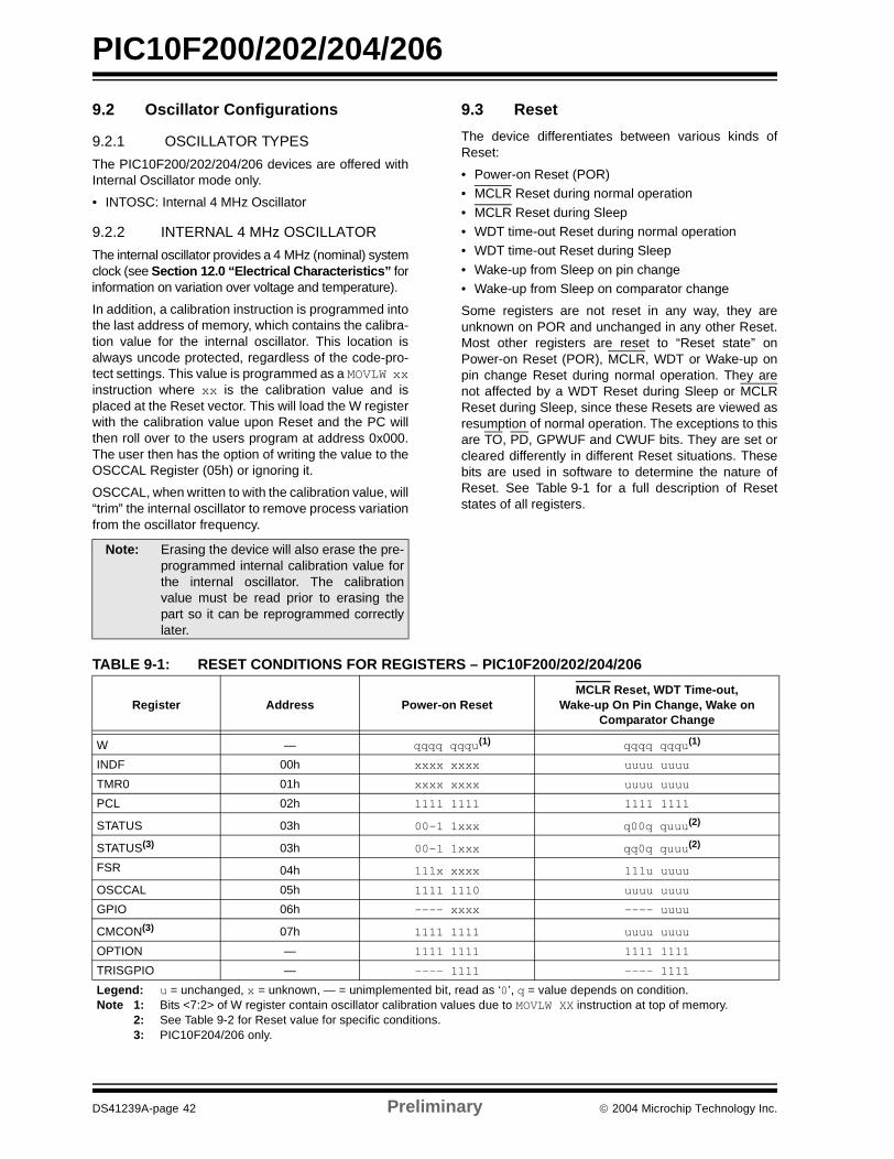
PIC10F200/202/204/206
9.2 Oscillator Configurations
9.2.1 OSCILLATOR TYPES
The PIC10F200/202/204/206 devices are offered withInternal Oscillator mode only.
• INTOSC: Internal 4 MHz Oscillator
9.2.2 INTERNAL 4 MHz OSCILLATOR
The internal oscillator provides a 4 MHz (nominal) systemclock (see Section 12.0 “Electrical Characteristics” forinformation on variation over voltage and temperature).
In addition, a calibration instruction is programmed intothe last address of memory, which contains the calibra-tion value for the internal oscillator. This location isalways uncode protected, regardless of the code-pro-tect settings. This value is programmed as a MOVLW xxinstruction where xx is the calibration value and isplaced at the Reset vector. This will load the W registerwith the calibration value upon Reset and the PC willthen roll over to the users program at address 0x000.The user then has the option of writing the value to theOSCCAL Register (05h) or ignoring it.
OSCCAL, when written to with the calibration value, will“trim” the internal oscillator to remove process variationfrom the oscillator frequency.
9.3 Reset
The device differentiates between various kinds ofReset:
• Power-on Reset (POR) • MCLR Reset during normal operation
• MCLR Reset during Sleep • WDT time-out Reset during normal operation• WDT time-out Reset during Sleep
• Wake-up from Sleep on pin change• Wake-up from Sleep on comparator change
Some registers are not reset in any way, they areunknown on POR and unchanged in any other Reset.Most other registers are reset to “Reset state” onPower-on Reset (POR), MCLR, WDT or Wake-up onpin change Reset during normal operation. They arenot affected by a WDT Reset during Sleep or MCLRReset during Sleep, since these Resets are viewed asresumption of normal operation. The exceptions to thisare TO, PD, GPWUF and CWUF bits. They are set orcleared differently in different Reset situations. Thesebits are used in software to determine the nature ofReset. See Table 9-1 for a full description of Resetstates of all registers.
TABLE 9-1: RESET CONDITIONS FOR REGISTERS – PIC10F200/202/204/206
Note: Erasing the device will also erase the pre-programmed internal calibration value forthe internal oscillator. The calibrationvalue must be read prior to erasing thepart so it can be reprogrammed correctlylater.
Register Address Power-on ResetMCLR Reset, WDT Time-out,
Wake-up On Pin Change, Wake on Comparator Change
W — qqqq qqqu(1) qqqq qqqu(1)
INDF 00h xxxx xxxx uuuu uuuu
TMR0 01h xxxx xxxx uuuu uuuu
PCL 02h 1111 1111 1111 1111
STATUS 03h 00-1 1xxx q00q quuu(2)
STATUS(3) 03h 00-1 1xxx qq0q quuu(2)
FSR 04h 111x xxxx 111u uuuu
OSCCAL 05h 1111 1110 uuuu uuuu
GPIO 06h ---- xxxx ---- uuuu
CMCON(3) 07h 1111 1111 uuuu uuuu
OPTION — 1111 1111 1111 1111
TRISGPIO — ---- 1111 ---- 1111
Legend: u = unchanged, x = unknown, — = unimplemented bit, read as ‘0’, q = value depends on condition.Note 1: Bits <7:2> of W register contain oscillator calibration values due to MOVLW XX instruction at top of memory.
2: See Table 9-2 for Reset value for specific conditions.3: PIC10F204/206 only.
DS41239A-page 42 Preliminary 2004 Microchip Technology Inc.

PIC10F200/202/204/206
TABLE 9-2: RESET CONDITION FOR SPECIAL REGISTERS
9.3.1 MCLR ENABLE
This configuration bit, when unprogrammed (left in the‘1’ state), enables the external MCLR function. Whenprogrammed, the MCLR function is tied to the internalVDD and the pin is assigned to be a I/O. See Figure 9-1.
FIGURE 9-1: MCLR SELECT
9.4 Power-on Reset (POR)
The PIC10F200/202/204/206 devices incorporate anon-chip Power-on Reset (POR) circuitry, whichprovides an internal chip Reset for most power-upsituations.
The on-chip POR circuit holds the chip in Reset untilVDD has reached a high enough level for proper oper-ation. To take advantage of the internal POR, programthe GP3/MCLR/VPP pin as MCLR and tie through aresistor to VDD, or program the pin as GP3. An internalweak pull-up resistor is implemented using a transistor(refer to Table 12-3 for the pull-up resistor ranges).This will eliminate external RC components usuallyneeded to create a Power-on Reset. A maximum risetime for VDD is specified. See Section 12.0 “ElectricalCharacteristics” for details.
When the devices start normal operation (exit theReset condition), device operating parameters (volt-age, frequency, temperature,...) must be met to ensureoperation. If these conditions are not met, the devicesmust be held in Reset until the operating parametersare met.
A simplified block diagram of the on-chip Power-onReset circuit is shown in Figure 9-2.
The Power-on Reset circuit and the Device ResetTimer (see Section 9.5 “Device Reset Timer (DRT)”)circuit are closely related. On power-up, the Reset latchis set and the DRT is reset. The DRT timer beginscounting once it detects MCLR to be high. After thetime-out period, which is typically 18 ms, it will reset theReset latch and thus end the on-chip Reset signal.
A power-up example where MCLR is held low is shownin Figure 9-3. VDD is allowed to rise and stabilize beforebringing MCLR high. The chip will actually come out ofReset TDRT msec after MCLR goes high.
In Figure 9-4, the on-chip Power-on Reset feature isbeing used (MCLR and VDD are tied together or the pinis programmed to be GP3). The VDD is stable beforethe Start-up timer times out and there is no problem ingetting a proper Reset. However, Figure 9-5 depicts aproblem situation where VDD rises too slowly. The timebetween when the DRT senses that MCLR is high andwhen MCLR and VDD actually reach their full value, istoo long. In this situation, when the start-up timer timesout, VDD has not reached the VDD (min) value and thechip may not function correctly. For such situations, werecommend that external RC circuits be used toachieve longer POR delay times (Figure 9-4).
For additional information, refer to Application NotesAN522 “Power-Up Considerations”, (DS00522) andAN607 “Power-up Trouble Shooting”, (DS00607).
STATUS Addr: 03h PCL Addr: 02h
Power-on Reset 00-1 1xxx 1111 1111
MCLR Reset during normal operation 000u uuuu 1111 1111
MCLR Reset during Sleep 0001 0uuu 1111 1111
WDT Reset during Sleep 0000 0uuu 1111 1111
WDT Reset normal operation 0000 uuuu 1111 1111
Wake-up from Sleep on pin change 1001 0uuu 1111 1111
Wake-up from Sleep on comparator change 0101 0uuu 1111 1111
Legend: u = unchanged, x = unknown, — = unimplemented bit, read as ‘0’.
GP3/MCLR/VPP
MCLRE Internal MCLR
GPWU
Note: When the devices start normal operation(exit the Reset condition), device operat-ing parameters (voltage, frequency,temperature, etc.) must be met to ensureoperation. If these conditions are not met,the device must be held in Reset until theoperating conditions are met.
2004 Microchip Technology Inc. Preliminary DS41239A-page 43

PIC10F200/202/204/206
FIGURE 9-2: SIMPLIFIED BLOCK DIAGRAM OF ON-CHIP RESET CIRCUIT
FIGURE 9-3: TIME-OUT SEQUENCE ON POWER-UP (MCLR PULLED LOW)
FIGURE 9-4: TIME-OUT SEQUENCE ON POWER-UP (MCLR TIED TO VDD): FAST VDD RISE TIME
S Q
R Q
VDD
GP3/MCLR/VPP
Power-upDetect POR (Power-on Reset)
WDT ResetCHIP Reset
MCLRE
Wake-up on pin change Reset
Start-up Timer
(10 µs or 18 ms)
WDT Time-out
Pin ChangeSleep
MCLR Reset
VDD
MCLR
Internal POR
DRT Time-out
Internal Reset
TDRT
VDD
MCLR
Internal POR
DRT Time-out
Internal Reset
TDRT
DS41239A-page 44 Preliminary 2004 Microchip Technology Inc.

PIC10F200/202/204/206
FIGURE 9-5: TIME-OUT SEQUENCE ON POWER-UP (MCLR TIED TO VDD): SLOW VDD RISE TIME
VDD
MCLR
Internal POR
DRT Time-out
Internal Reset
TDRT
V1
Note: When VDD rises slowly, the TDRT time-out expires long before VDD has reached its finalvalue. In this example, the chip will reset properly if, and only if, V1 ≥ VDD min.
2004 Microchip Technology Inc. Preliminary DS41239A-page 45

PIC10F200/202/204/206
9.5 Device Reset Timer (DRT)
On the PIC10F200/202/204/206 devices, the DRT runsany time the device is powered up.
The DRT operates on an internal oscillator. Theprocessor is kept in Reset as long as the DRT is active.The DRT delay allows VDD to rise above VDD min. andfor the oscillator to stabilize.
The on-chip DRT keeps the devices in a Resetcondition for approximately 18 ms after MCLR hasreached a logic high (VIH MCLR) level. ProgrammingGP3/MCLR/VPP as MCLR and using an external RCnetwork connected to the MCLR input is not required inmost cases. This allows savings in cost-sensitive and/or space restricted applications, as well as allowing theuse of the GP3/MCLR/VPP pin as a general purposeinput.
The Device Reset Time delays will vary from chip-to-chip due to VDD, temperature and process variation.See AC parameters for details.
Reset sources are POR, MCLR, WDT time-out andwake-up on pin change. See Section 9.9.2 “Wake-upfrom Sleep”, Notes 1, 2 and 3.
TABLE 9-3: DRT (DEVICE RESET TIMER PERIOD)
9.6 Watchdog Timer (WDT)
The Watchdog Timer (WDT) is a free running on-chipRC oscillator, which does not require any externalcomponents. This RC oscillator is separate from theinternal 4 MHz oscillator. This means that the WDT willrun even if the main processor clock has been stopped,for example, by execution of a SLEEP instruction.During normal operation or Sleep, a WDT Reset orwake-up Reset, generates a device Reset.
The TO bit (Status<4>) will be cleared upon aWatchdog Timer Reset.
The WDT can be permanently disabled by program-ming the configuration WDTE as a ‘0’ (see Section 9.1“Configuration Bits”). Refer to the PIC10F200/202/204/206 Programming Specifications to determine howto access the Configuration Word.
9.6.1 WDT PERIOD
The WDT has a nominal time-out period of 18 ms, (withno prescaler). If a longer time-out period is desired, aprescaler with a division ratio of up to 1:128 can beassigned to the WDT (under software control) bywriting to the Option register. Thus, a time-out period ofa nominal 2.3 seconds can be realized. These periodsvary with temperature, VDD and part-to-part processvariations (see DC specs).
Under worst case conditions (VDD = Min., Temperature= Max., max. WDT prescaler), it may take severalseconds before a WDT time-out occurs.
9.6.2 WDT PROGRAMMING CONSIDERATIONS
The CLRWDT instruction clears the WDT and thepostscaler, if assigned to the WDT, and prevents it fromtiming out and generating a device Reset.
The SLEEP instruction resets the WDT and thepostscaler, if assigned to the WDT. This gives themaximum Sleep time before a WDT wake-up Reset.
Oscillator POR ResetSubsequent
Resets
INTOSC 18 ms (typical) 10 µs (typical)
DS41239A-page 46 Preliminary 2004 Microchip Technology Inc.

PIC10F200/202/204/206
FIGURE 9-6: WATCHDOG TIMER BLOCK DIAGRAM
TABLE 9-4: SUMMARY OF REGISTERS ASSOCIATED WITH THE WATCHDOG TIMER
Address Name Bit 7 Bit 6 Bit 5 Bit 4 Bit 3 Bit 2 Bit 1 Bit 0Value on
Power-OnReset
Value onAll Other Resets
N/A OPTION GPWU GPPU T0CS T0SE PSA PS2 PS1 PS0 1111 1111 1111 1111
Legend: Shaded boxes = Not used by Watchdog Timer, — = unimplemented, read as ‘0’, u = unchanged.
(Figure 6-5)
Postscaler
Note 1: T0CS, T0SE, PSA, PS<2:0> are bits in the Option register.
WDT Time-out
WatchdogTime
From Timer0 Clock Source
WDT EnableConfiguration
Bit
PSA
Postscaler
8-to-1 MUX PS<2:0>
(Figure 6-4)To Timer0
0
1MUX
10
PSAMUX
2004 Microchip Technology Inc. Preliminary DS41239A-page 47

PIC10F200/202/204/206
9.7 Time-out Sequence, Power-down and Wake-up from Sleep Status Bits (TO, PD, GPWUF, CWUF)
The TO, PD, GPWUF and CWUF bits in the Statusregister can be tested to determine if a Reset conditionhas been caused by a Power-up condition, a MCLR,Watchdog Timer (WDT) Reset, wake-up on comparatorchange or wake-up on pin change.
TABLE 9-5: TO, PD, GPWUF, CWUF STATUS AFTER RESET
9.8 Reset on Brown-out
A Brown-out is a condition where device power (VDD)dips below its minimum value, but not to zero, and thenrecovers. The device should be reset in the event of aBrown-out.
To reset PIC10F200/202/204/206 devices when aBrown-out occurs, external Brown-out protectioncircuits may be built, as shown in Figure 9-7 andFigure 9-8.
FIGURE 9-7: BROWN-OUT PROTECTION CIRCUIT 1
FIGURE 9-8: BROWN-OUT PROTECTION CIRCUIT 2
CWUF GPWUF TO PD Reset Caused By
0 0 0 0 WDT wake-up from Sleep
0 0 0 u WDT time-out (not from Sleep)
0 0 1 0 MCLR wake-up from Sleep
0 0 1 1 Power-up
0 0 u u MCLR not during Sleep
0 1 1 0 Wake-up from Sleep on pin change
1 0 1 0 Wake-up from Sleep on comparator change
Legend: u = unchanged, x = unknown, — = unimplemented bit, read as ‘0’, q = value depends on condition.Note 1: The TO, PD, GPWUF and CWUF bits maintain their status (u) until a Reset occurs. A low-pulse on the
MCLR input does not change the TO, PD, GPWUF or CWUF status bits.
Note 1: This circuit will activate Reset when VDD goes below Vz + 0.7V (where Vz = Zener voltage).
2: Pin must be confirmed as MCLR.
33k
10k
40k(1)
VDD
MCLR(2)PIC10F20X
VDD
Q1
Note 1: This brown-out circuit is less expensive, although less accurate. Transistor Q1 turns off when VDD is below a certain level such that:
2: Pin must be confirmed as MCLR.
VDD •R1
R1 + R2= 0.7V
R2 40k(1)
VDD
MCLR(2)PIC10F20X
R1
Q1
VDD
DS41239A-page 48 Preliminary 2004 Microchip Technology Inc.

PIC10F200/202/204/206
FIGURE 9-9: BROWN-OUT PROTECTION CIRCUIT 3
9.9 Power-down Mode (Sleep)
A device may be powered down (Sleep) and laterpowered up (wake-up from Sleep).
9.9.1 SLEEP
The Power-down mode is entered by executing aSLEEP instruction.
If enabled, the Watchdog Timer will be cleared butkeeps running, the TO bit (Status<4>) is set, the PD bit(Status<3>) is cleared and the oscillator driver is turnedoff. The I/O ports maintain the status they had beforethe SLEEP instruction was executed (driving high,driving low or high-impedance).
For lowest current consumption while powered down,the T0CKI input should be at VDD or VSS and the GP3/MCLR/VPP pin must be at a logic high level if MCLR isenabled.
9.9.2 WAKE-UP FROM SLEEP
The device can wake-up from Sleep through one ofthe following events:
1. An external Reset input on GP3/MCLR/VPP pin,when configured as MCLR.
2. A Watchdog Timer time-out Reset (if WDT wasenabled).
3. A change on input pin GP0, GP1 or GP3 whenwake-up on change is enabled.
4. A comparator output change has occurred whenwake-up on comparator change is enabled.
These events cause a device Reset. The TO, PDGPWUF and CWUF bits can be used to determine thecause of device Reset. The TO bit is cleared if a WDTtime-out occurred (and caused wake-up). The PD bit,which is set on power-up, is cleared when SLEEP isinvoked. The GPWUF bit indicates a change in statewhile in Sleep at pins GP0, GP1 or GP3 (since the lastfile or bit operation on GP port). The CWUF bitindicates a change in the state while in Sleep of thecomparator output.
Note: A Reset generated by a WDT time-outdoes not drive the MCLR pin low.
Note: This Brown-out Protection circuit employsMicrochip Technology’s MCP809 micro-controller supervisor. There are 7 differenttrip point selections to accommodate 5V to3V systems.
MCLR
PIC10F20X
VDD
VDDVSS
RST
MCP809
VDD
BypassCapacitor
Note: Caution: Right before entering Sleep,read the input pins. When in Sleep, wake-up occurs when the values at the pinschange from the state they were in at thelast reading. If a wake-up on changeoccurs and the pins are not read before re-entering Sleep, a wake-up will occurimmediately even if no pins change whilein Sleep mode.
Note: The WDT is cleared when the devicewakes from Sleep, regardless of the wake-up source.
2004 Microchip Technology Inc. Preliminary DS41239A-page 49
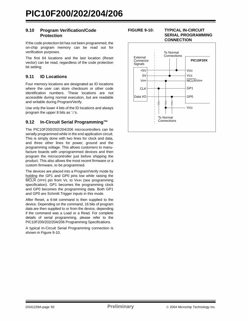
PIC10F200/202/204/206
9.10 Program Verification/Code Protection
If the code protection bit has not been programmed, theon-chip program memory can be read out forverification purposes.
The first 64 locations and the last location (Resetvector) can be read, regardless of the code protectionbit setting.
9.11 ID Locations
Four memory locations are designated as ID locationswhere the user can store checksum or other codeidentification numbers. These locations are notaccessible during normal execution, but are readableand writable during Program/Verify.
Use only the lower 4 bits of the ID locations and alwaysprogram the upper 8 bits as ‘0’s.
9.12 In-Circuit Serial Programming™
The PIC10F200/202/204/206 microcontrollers can beserially programmed while in the end application circuit.This is simply done with two lines for clock and data,and three other lines for power, ground and theprogramming voltage. This allows customers to manu-facture boards with unprogrammed devices and thenprogram the microcontroller just before shipping theproduct. This also allows the most recent firmware or acustom firmware, to be programmed.
The devices are placed into a Program/Verify mode byholding the GP1 and GP0 pins low while raising theMCLR (VPP) pin from VIL to VIHH (see programmingspecification). GP1 becomes the programming clockand GP0 becomes the programming data. Both GP1and GP0 are Schmitt Trigger inputs in this mode.
After Reset, a 6-bit command is then supplied to thedevice. Depending on the command, 16 bits of programdata are then supplied to or from the device, dependingif the command was a Load or a Read. For completedetails of serial programming, please refer to thePIC10F200/202/204/206 Programming Specifications.
A typical In-Circuit Serial Programming connection isshown in Figure 9-10.
FIGURE 9-10: TYPICAL IN-CIRCUIT SERIAL PROGRAMMING CONNECTION
ExternalConnectorSignals
To NormalConnections
To NormalConnections
PIC10F20X
VDD
VSS
MCLR/VPP
GP1
GP0
+5V
0V
VPP
CLK
Data I/O
VDD
DS41239A-page 50 Preliminary 2004 Microchip Technology Inc.

PIC10F200/202/204/206
10.0 INSTRUCTION SET SUMMARY
The PIC16 instruction set is highly orthogonal and iscomprised of three basic categories.
• Byte-oriented operations
• Bit-oriented operations• Literal and control operations
Each PIC16 instruction is a 12-bit word divided into anopcode, which specifies the instruction type and one ormore operands which further specify the operation ofthe instruction. The formats for each of the categoriesis presented in Figure 10-1, while the various opcodefields are summarized in Table 10-1.
For byte-oriented instructions, ‘f’ represents a fileregister designator and ‘d’ represents a destinationdesignator. The file register designator specifies whichfile register is to be used by the instruction.
The destination designator specifies where the result ofthe operation is to be placed. If ‘d’ is ‘0’, the result isplaced in the W register. If ‘d’ is ‘1’, the result is placedin the file register specified in the instruction.
For bit-oriented instructions, ‘b’ represents a bit fielddesignator which selects the number of the bit affectedby the operation, while ‘f’ represents the number of thefile in which the bit is located.
For literal and control operations, ‘k’ represents an8 or 9-bit constant or literal value.
TABLE 10-1: OPCODE FIELD DESCRIPTIONS
All instructions are executed within a single instructioncycle, unless a conditional test is true or the programcounter is changed as a result of an instruction. In thiscase, the execution takes two instruction cycles. Oneinstruction cycle consists of four oscillator periods.Thus, for an oscillator frequency of 4 MHz, the normalinstruction execution time is 1 µs. If a conditional test istrue or the program counter is changed as a result of aninstruction, the instruction execution time is 2 µs.
Figure 10-1 shows the three general formats that theinstructions can have. All examples in the figure usethe following format to represent a hexadecimalnumber:
0xhhh
where ‘h’ signifies a hexadecimal digit.
FIGURE 10-1: GENERAL FORMAT FOR INSTRUCTIONS
Field Description
f Register file address (0x00 to 0x7F)
W Working register (accumulator)
b Bit address within an 8-bit file register
k Literal field, constant data or label
x Don’t care location (= 0 or 1) The assembler will generate code with x = 0. It is the recommended form of use for compatibility with all Microchip software tools.
d Destination select; d = 0 (store result in W)d = 1 (store result in file register ‘f’)Default is d = 1
label Label name
TOS Top-of-Stack
PC Program Counter
WDT Watchdog Timer counter
TO Time-out bit
PD Power-down bit
dest Destination, either the W register or the specifiedregister file location
[ ] Options
( ) Contents
→ Assigned to
< > Register bit field
∈ In the set of
italics User defined term (font is courier)
Byte-oriented file register operations
11 6 5 4 0
d = 0 for destination W
OPCODE d f (FILE #)
d = 1 for destination ff = 5-bit file register address
Bit-oriented file register operations
11 8 7 5 4 0
OPCODE b (BIT #) f (FILE #)
b = 3-bit addressf = 5-bit file register address
Literal and control operations (except GOTO)
11 8 7 0
OPCODE k (literal)
k = 8-bit immediate value
Literal and control operations – GOTO instruction
11 9 8 0
OPCODE k (literal)
k = 9-bit immediate value
2004 Microchip Technology Inc. Preliminary DS41239A-page 51

PIC10F200/202/204/206
TABLE 10-2: INSTRUCTION SET SUMMARY
Mnemonic,Operands
Description Cycles12-Bit Opcode Status
AffectedNotes
MSb LSb
ADDWFANDWFCLRFCLRWCOMFDECFDECFSZINCFINCFSZIORWFMOVFMOVWFNOPRLFRRFSUBWFSWAPFXORWF
f, df, df–f, df, df, df, df, df, df, df–f, df, df, df, df, d
Add W and fAND W with fClear fClear WComplement fDecrement fDecrement f, Skip if 0Increment fIncrement f, Skip if 0Inclusive OR W with fMove fMove W to fNo OperationRotate left f through CarryRotate right f through CarrySubtract W from fSwap fExclusive OR W with f
111111
1(2)
11(2)
111111111
000100010000000000100000001000100011000100100000000000110011000000110001
11df01df011f010001df11df11df10df11df00df00df001f000001df00df10df10df10df
ffffffffffff0000ffffffffffffffffffffffffffffffff0000ffffffffffffffffffff
C, DC, ZZZZZZ
NoneZ
NoneZZ
NoneNone
CC
C, DC, ZNone
Z
1, 2, 42, 4
4
2, 42, 42, 42, 42, 42, 41, 4
2, 42, 4
1, 2, 42, 42, 4
BIT-ORIENTED FILE REGISTER OPERATIONSBCFBSFBTFSCBTFSS
f, bf, bf, bf, b
Bit Clear fBit Set fBit Test f, Skip if ClearBit Test f, Skip if Set
11
1(2)
1(2)
0100010101100111
bbbfbbbfbbbfbbbf
ffffffffffffffff
NoneNoneNoneNone
2, 42, 4
LITERAL AND CONTROL OPERATIONSANDLWCALLCLRWDTGOTOIORLWMOVLWOPTIONRETLWSLEEPTRISXORLW
kk
kkk–k–fk
AND literal with WCall SubroutineClear Watchdog TimerUnconditional branchInclusive OR literal with WMove literal to WLoad Option registerReturn, place Literal in WGo into Standby modeLoad TRIS registerExclusive OR literal to W
12121112111
111010010000101k1101110000001000000000001111
kkkkkkkk0000kkkkkkkkkkkk0000kkkk00000000kkkk
kkkkkkkk0100kkkkkkkkkkkk0010kkkk00110fffkkkk
ZNone
TO, PDNone
ZNoneNoneNone
TO, PDNone
Z
1
3
Note 1: The 9th bit of the program counter will be forced to a ‘0’ by any instruction that writes to the PC except for GOTO. See Section 4.7 “Program Counter”.
2: When an I/O register is modified as a function of itself (e.g. MOVF PORTB, 1), the value used will be that value present on the pins themselves. For example, if the data latch is ‘1’ for a pin configured as input and is driven low by an external device, the data will be written back with a ‘0’.
3: The instruction TRIS f, where f = 6, causes the contents of the W register to be written to the tri-state latches of PORTB. A ‘1’ forces the pin to a high-impedance state and disables the output buffers.
4: If this instruction is executed on the TMR0 register (and where applicable, d = 1), the prescaler will be cleared (if assigned to TMR0).
DS41239A-page 52 Preliminary 2004 Microchip Technology Inc.

PIC10F200/202/204/206
ADDWF Add W and f
Syntax: [ label ] ADDWF f,d
Operands: 0 ≤ f ≤ 31d ∈ [ 0,1]
Operation: (W) + (f) → (dest)
Status Affected: C, DC, Z
Description: Add the contents of the W register and register ‘f’. If ‘d’ is ‘0’, the result is stored in the W register. If ‘d’ is ‘1’, the result is stored back in register ‘f’.
ANDLW AND literal with W
Syntax: [ label ] ANDLW k
Operands: 0 ≤ k ≤ 255
Operation: (W).AND. (k) → (W)
Status Affected: Z
Description: The contents of the W register are AND’ed with the eight-bit literal ‘k’. The result is placed in the W register.
ANDWF AND W with f
Syntax: [ label ] ANDWF f,d
Operands: 0 ≤ f ≤ 31d ∈ [0,1]
Operation: (W) .AND. (f) → (dest)
Status Affected: Z
Description: The contents of the W register are AND’ed with register ‘f’. If ‘d’ is ‘0’, the result is stored in the W register. If ‘d’ is ‘1’, the result is stored back in register ‘f’.
BCF Bit Clear f
Syntax: [ label ] BCF f,b
Operands: 0 ≤ f ≤ 310 ≤ b ≤ 7
Operation: 0 → (f<b>)
Status Affected: None
Description: Bit ‘b’ in register ‘f’ is cleared.
BSF Bit Set f
Syntax: [ label ] BSF f,b
Operands: 0 ≤ f ≤ 310 ≤ b ≤ 7
Operation: 1 → (f<b>)
Status Affected: None
Description: Bit ‘b’ in register ‘f’ is set.
BTFSC Bit Test f, Skip if Clear
Syntax: [ label ] BTFSC f,b
Operands: 0 ≤ f ≤ 310 ≤ b ≤ 7
Operation: skip if (f<b>) = 0
Status Affected: None
Description: If bit ‘b’ in register ‘f’ is ‘0’, then the next instruction is skipped.
If bit ‘b’ is ‘0’, then the next instruc-tion fetched during the current instruction execution is discarded, and a NOP is executed instead, making this a 2-cycle instruction.
2004 Microchip Technology Inc. Preliminary DS41239A-page 53

PIC10F200/202/204/206
BTFSS Bit Test f, Skip if Set
Syntax: [ label ] BTFSS f,b
Operands: 0 ≤ f ≤ 310 ≤ b < 7
Operation: skip if (f<b>) = 1
Status Affected: None
Description: If bit ‘b’ in register ‘f’ is ‘1’, then the next instruction is skipped.
If bit ‘b’ is ‘1’, then the next instruc-tion fetched during the current instruction execution, is discarded and a NOP is executed instead, making this a 2-cycle instruction.
CALL Subroutine Call
Syntax: [ label ] CALL k
Operands: 0 ≤ k ≤ 255
Operation: (PC) + 1→ Top-of-Stack;k → PC<7:0>;(Status<6:5>) → PC<10:9>;0 → PC<8>
Status Affected: None
Description: Subroutine call. First, return address (PC + 1) is pushed onto the stack. The eight-bit immediate address is loaded into PC bits <7:0>. The upper bits PC<10:9> are loaded from Status<6:5>, PC<8> is cleared. CALL is a two-cycle instruction.
CLRF Clear f
Syntax: [ label ] CLRF f
Operands: 0 ≤ f ≤ 31
Operation: 00h → (f);1 → Z
Status Affected: Z
Description: The contents of register ‘f’ are cleared and the Z bit is set.
CLRW Clear W
Syntax: [ label ] CLRW
Operands: None
Operation: 00h → (W);1 → Z
Status Affected: Z
Description: The W register is cleared. Zero bit (Z) is set.
CLRWDT Clear Watchdog Timer
Syntax: [ label ] CLRWDT
Operands: None
Operation: 00h → WDT;0 → WDT prescaler (if assigned);1 → TO;1 → PD
Status Affected: TO, PD
Description: The CLRWDT instruction resets the WDT. It also resets the prescaler, if the prescaler is assigned to the WDT and not Timer0. Status bits TO and PD are set.
COMF Complement f
Syntax: [ label ] COMF f,d
Operands: 0 ≤ f ≤ 31d ∈ [0,1]
Operation: (f) → (dest)
Status Affected: Z
Description: The contents of register ‘f’ are complemented. If ‘d’ is ‘0’, the result is stored in the W register. If ‘d’ is ‘1’, the result is stored back in register ‘f’.
DS41239A-page 54 Preliminary 2004 Microchip Technology Inc.

PIC10F200/202/204/206
DECF Decrement f
Syntax: [ label ] DECF f,d
Operands: 0 ≤ f ≤ 31d ∈ [0,1]
Operation: (f) – 1 → (dest)
Status Affected: Z
Description: Decrement register ‘f’. If ‘d’ is ‘0’, the result is stored in the W register. If ‘d’ is ‘1’, the result is stored back in register ‘f’.
DECFSZ Decrement f, Skip if 0
Syntax: [ label ] DECFSZ f,d
Operands: 0 ≤ f ≤ 31d ∈ [0,1]
Operation: (f) – 1 → d; skip if result = 0
Status Affected: None
Description: The contents of register ‘f’ are decremented. If ‘d’ is ‘0’, the result is placed in the W register. If ‘d’ is ‘1’, the result is placed back in register ‘f’.If the result is ‘0’, the next instruc-tion, which is already fetched, is discarded and a NOP is executed instead making it a two-cycle instruction.
GOTO Unconditional Branch
Syntax: [ label ] GOTO k
Operands: 0 ≤ k ≤ 511
Operation: k → PC<8:0>;Status<6:5> → PC<10:9>
Status Affected: None
Description: GOTO is an unconditional branch. The 9-bit immediate value is loaded into PC bits <8:0>. The upper bits of PC are loaded from Status<6:5>. GOTO is a two-cycle instruction.
INCF Increment f
Syntax: [ label ] INCF f,d
Operands: 0 ≤ f ≤ 31d ∈ [0,1]
Operation: (f) + 1 → (dest)
Status Affected: Z
Description: The contents of register ‘f’ are incremented. If ‘d’ is ‘0’, the result is placed in the W register. If ‘d’ is ‘1’, the result is placed back in register ‘f’.
INCFSZ Increment f, Skip if 0
Syntax: [ label ] INCFSZ f,d
Operands: 0 ≤ f ≤ 31d ∈ [0,1]
Operation: (f) + 1 → (dest), skip if result = 0
Status Affected: None
Description: The contents of register ‘f’ are incremented. If ‘d’ is ‘0’, the result is placed in the W register. If ‘d’ is ‘1’, the result is placed back in register ‘f’.If the result is ‘0’, then the next instruction, which is already fetched, is discarded and a NOP is executed instead making it a two-cycle instruction.
IORLW Inclusive OR literal with W
Syntax: [ label ] IORLW k
Operands: 0 ≤ k ≤ 255
Operation: (W) .OR. (k) → (W)
Status Affected: Z
Description: The contents of the W register are OR’ed with the eight bit literal ‘k’. The result is placed in the W register.
2004 Microchip Technology Inc. Preliminary DS41239A-page 55

PIC10F200/202/204/206
IORWF Inclusive OR W with f
Syntax: [ label ] IORWF f,d
Operands: 0 ≤ f ≤ 31d ∈ [0,1]
Operation: (W).OR. (f) → (dest)
Status Affected: Z
Description: Inclusive OR the W register with register ‘f’. If ‘d’ is ‘0’, the result is placed in the W register. If ‘d’ is ‘1’, the result is placed back in register ‘f’.
MOVF Move f
Syntax: [ label ] MOVF f,d
Operands: 0 ≤ f ≤ 31d ∈ [0,1]
Operation: (f) → (dest)
Status Affected: Z
Description: The contents of register ‘f’ are moved to destination ‘d’. If ‘d’ is ‘0’, destination is the W register. If ‘d’ is ‘1’, the destination is file register ‘f’. ‘d’ = 1 is useful as a test of a file register, since status flag Z is affected.
MOVLW Move literal to W
Syntax: [ label ] MOVLW k
Operands: 0 ≤ k ≤ 255
Operation: k → (W)
Status Affected: None
Description: The eight-bit literal ‘k’ is loaded into the W register. The don’t cares will assembled as ‘0’s.
MOVWF Move W to f
Syntax: [ label ] MOVWF f
Operands: 0 ≤ f ≤ 31
Operation: (W) → (f)
Status Affected: None
Description: Move data from the W register to register ‘f’.
NOP No Operation
Syntax: [ label ] NOP
Operands: None
Operation: No operation
Status Affected: None
Description: No operation.
OPTION Load Option Register
Syntax: [ label ] Option
Operands: None
Operation: (W) → Option
Status Affected: None
Description: The content of the W register is loaded into the Option register.
DS41239A-page 56 Preliminary 2004 Microchip Technology Inc.

PIC10F200/202/204/206
RETLW Return with literal in W
Syntax: [ label ] RETLW k
Operands: 0 ≤ k ≤ 255
Operation: k → (W);TOS → PC
Status Affected: None
Description: The W register is loaded with the eight-bit literal ‘k’. The program counter is loaded from the top of the stack (the return address). This is a two-cycle instruction.
RLF Rotate Left f through Carry
Syntax: [ label ] RLF f,d
Operands: 0 ≤ f ≤ 31d ∈ [0,1]
Operation: See description below
Status Affected: C
Description: The contents of register ‘f’ are rotated one bit to the left through the Carry flag. If ‘d’ is ‘0’, the result is placed in the W register. If ‘d’ is ‘1’, the result is stored back in reg-ister ‘f’.
RRF Rotate Right f through Carry
Syntax: [ label ] RRF f,d
Operands: 0 ≤ f ≤ 31d ∈ [0,1]
Operation: See description below
Status Affected: C
Description: The contents of register ‘f’ are rotated one bit to the right through the Carry flag. If ‘d’ is ‘0’, the result is placed in the W register. If ‘d’ is ‘1’, the result is placed back in register ‘f’.
C register ‘f’
C register ‘f’
SLEEP Enter SLEEP Mode
Syntax: [ label ] SLEEP
Operands: None
Operation: 00h → WDT;0 → WDT prescaler;1 → TO;0 → PD
Status Affected: TO, PD, RBWUF
Description: Time-out Status bit (TO) is set. The Power-down Status bit (PD) is cleared. RBWUF is unaffected.
The WDT and its prescaler are cleared.
The processor is put into Sleep mode with the oscillator stopped. See Section 9.9 “Power-down Mode (Sleep)” for more details.
SUBWF Subtract W from f
Syntax: [ label ] SUBWF f,d
Operands: 0 ≤ f ≤ 31d ∈ [0,1]
Operation: (f) – (W) → (dest)
Status Affected: C, DC, Z
Description: Subtract (2’s complement method) the W register from register ‘f’. If ‘d’ is ‘0’, the result is stored in the W register. If ‘d’ is ‘1’, the result is stored back in register ‘f’.
SWAPF Swap Nibbles in f
Syntax: [ label ] SWAPF f,d
Operands: 0 ≤ f ≤ 31d ∈ [0,1]
Operation: (f<3:0>) → (dest<7:4>);(f<7:4>) → (dest<3:0>)
Status Affected: None
Description: The upper and lower nibbles of register ‘f’ are exchanged. If ‘d’ is ‘0’, the result is placed in W register. If ‘d’ is ‘1’, the result is placed in register ‘f’.
2004 Microchip Technology Inc. Preliminary DS41239A-page 57

PIC10F200/202/204/206
TRIS Load TRIS Register
Syntax: [ label ] TRIS f
Operands: f = 6
Operation: (W) → TRIS register f
Status Affected: None
Description: TRIS register ‘f’ (f = 6 or 7) is loaded with the contents of the W register
XORLW Exclusive OR literal with W
Syntax: [ label ] XORLW k
Operands: 0 ≤ k ≤ 255
Operation: (W) .XOR. k → (W)
Status Affected: Z
Description: The contents of the W register are XOR’ed with the eight-bit literal ‘k’. The result is placed in the W register.
XORWF Exclusive OR W with f
Syntax: [ label ] XORWF f,d
Operands: 0 ≤ f ≤ 31d ∈ [0,1]
Operation: (W) .XOR. (f) → (dest)
Status Affected: Z
Description: Exclusive OR the contents of the W register with register ‘f’. If ‘d’ is ‘0’, the result is stored in the W register. If ‘d’ is ‘1’, the result is stored back in register ‘f’.
DS41239A-page 58 Preliminary 2004 Microchip Technology Inc.

PIC10F200/202/204/206
11.0 DEVELOPMENT SUPPORT
The PICmicro® microcontrollers are supported with afull range of hardware and software development tools:
• Integrated Development Environment
- MPLAB® IDE Software• Assemblers/Compilers/Linkers
- MPASMTM Assembler
- MPLAB C17 and MPLAB C18 C Compilers- MPLINKTM Object Linker/
MPLIBTM Object Librarian- MPLAB C30 C Compiler- MPLAB ASM30 Assembler/Linker/Library
• Simulators- MPLAB SIM Software Simulator- MPLAB dsPIC30 Software Simulator
• Emulators- MPLAB ICE 2000 In-Circuit Emulator- MPLAB ICE 4000 In-Circuit Emulator
• In-Circuit Debugger- MPLAB ICD 2
• Device Programmers
- PRO MATE® II Universal Device Programmer- PICSTART® Plus Development Programmer- MPLAB PM3 Device Programmer
• Low-Cost Demonstration Boards- PICDEMTM 1 Demonstration Board- PICDEM.netTM Demonstration Board
- PICDEM 2 Plus Demonstration Board- PICDEM 3 Demonstration Board- PICDEM 4 Demonstration Board
- PICDEM 17 Demonstration Board- PICDEM 18R Demonstration Board- PICDEM LIN Demonstration Board
- PICDEM USB Demonstration Board• Evaluation Kits
- KEELOQ®
- PICDEM MSC- microID®
- CAN
- PowerSmart®
- Analog
11.1 MPLAB Integrated Development Environment Software
The MPLAB IDE software brings an ease of softwaredevelopment previously unseen in the 8/16-bit micro-controller market. The MPLAB IDE is a Windows®
based application that contains:
• An interface to debugging tools- simulator- programmer (sold separately)
- emulator (sold separately)- in-circuit debugger (sold separately)
• A full-featured editor with color coded context
• A multiple project manager• Customizable data windows with direct edit of
contents• High-level source code debugging• Mouse over variable inspection
• Extensive on-line help
The MPLAB IDE allows you to:
• Edit your source files (either assembly or C)• One touch assemble (or compile) and download
to PICmicro emulator and simulator tools (automatically updates all project information)
• Debug using:- source files (assembly or C)- mixed assembly and C
- machine code
MPLAB IDE supports multiple debugging tools in asingle development paradigm, from the cost effectivesimulators, through low-cost in-circuit debuggers, tofull-featured emulators. This eliminates the learningcurve when upgrading to tools with increasing flexibilityand power.
11.2 MPASM Assembler
The MPASM assembler is a full-featured, universalmacro assembler for all PICmicro MCUs.
The MPASM assembler generates relocatable objectfiles for the MPLINK object linker, Intel® standard HEXfiles, MAP files to detail memory usage and symbol ref-erence, absolute LST files that contain source lines andgenerated machine code and COFF files fordebugging.
The MPASM assembler features include:
• Integration into MPLAB IDE projects• User defined macros to streamline assembly code
• Conditional assembly for multi-purpose source files
• Directives that allow complete control over the assembly process
2004 Microchip Technology Inc. Preliminary DS41239A-page 59

PIC10F200/202/204/206
11.3 MPLAB C17 and MPLAB C18 C Compilers
The MPLAB C17 and MPLAB C18 Code DevelopmentSystems are complete ANSI C compilers forMicrochip’s PIC17CXXX and PIC18CXXX family ofmicrocontrollers. These compilers provide powerfulintegration capabilities, superior code optimization andease of use not found with other compilers.
For easy source level debugging, the compilers providesymbol information that is optimized to the MPLAB IDEdebugger.
11.4 MPLINK Object Linker/MPLIB Object Librarian
The MPLINK object linker combines relocatableobjects created by the MPASM assembler and theMPLAB C17 and MPLAB C18 C compilers. It can linkrelocatable objects from precompiled libraries, usingdirectives from a linker script.
The MPLIB object librarian manages the creation andmodification of library files of precompiled code. Whena routine from a library is called from a source file, onlythe modules that contain that routine will be linked inwith the application. This allows large libraries to beused efficiently in many different applications.
The object linker/library features include:
• Efficient linking of single libraries instead of many smaller files
• Enhanced code maintainability by grouping related modules together
• Flexible creation of libraries with easy module listing, replacement, deletion and extraction
11.5 MPLAB C30 C Compiler
The MPLAB C30 C compiler is a full-featured, ANSIcompliant, optimizing compiler that translates standardANSI C programs into dsPIC30F assembly languagesource. The compiler also supports many commandline options and language extensions to take fulladvantage of the dsPIC30F device hardware capabili-ties and afford fine control of the compiler codegenerator.
MPLAB C30 is distributed with a complete ANSI Cstandard library. All library functions have been vali-dated and conform to the ANSI C library standard. Thelibrary includes functions for string manipulation,dynamic memory allocation, data conversion, time-keeping and math functions (trigonometric, exponentialand hyperbolic). The compiler provides symbolicinformation for high-level source debugging with theMPLAB IDE.
11.6 MPLAB ASM30 Assembler, Linker and Librarian
MPLAB ASM30 assembler produces relocatablemachine code from symbolic assembly language fordsPIC30F devices. MPLAB C30 compiler uses theassembler to produce it’s object file. The assemblergenerates relocatable object files that can then bearchived or linked with other relocatable object files andarchives to create an executable file. Notable featuresof the assembler include:
• Support for the entire dsPIC30F instruction set
• Support for fixed-point and floating-point data• Command line interface• Rich directive set
• Flexible macro language• MPLAB IDE compatibility
11.7 MPLAB SIM Software Simulator
The MPLAB SIM software simulator allows code devel-opment in a PC hosted environment by simulating thePICmicro series microcontrollers on an instructionlevel. On any given instruction, the data areas can beexamined or modified and stimuli can be applied froma file, or user defined key press, to any pin. The execu-tion can be performed in Single-Step, Execute UntilBreak or Trace mode.
The MPLAB SIM simulator fully supports symbolicdebugging using the MPLAB C17 and MPLAB C18C Compilers, as well as the MPASM assembler. Thesoftware simulator offers the flexibility to develop anddebug code outside of the laboratory environment,making it an excellent, economical softwaredevelopment tool.
11.8 MPLAB SIM30 Software Simulator
The MPLAB SIM30 software simulator allows codedevelopment in a PC hosted environment by simulatingthe dsPIC30F series microcontrollers on an instructionlevel. On any given instruction, the data areas can beexamined or modified and stimuli can be applied froma file, or user defined key press, to any of the pins.
The MPLAB SIM30 simulator fully supports symbolicdebugging using the MPLAB C30 C Compiler andMPLAB ASM30 assembler. The simulator runs in eithera Command Line mode for automated tasks, or fromMPLAB IDE. This high-speed simulator is designed todebug, analyze and optimize time intensive DSProutines.
DS41239A-page 60 Preliminary 2004 Microchip Technology Inc.

PIC10F200/202/204/206
11.9 MPLAB ICE 2000 High-Performance Universal In-Circuit Emulator
The MPLAB ICE 2000 universal in-circuit emulator isintended to provide the product development engineerwith a complete microcontroller design tool set forPICmicro microcontrollers. Software control of theMPLAB ICE 2000 in-circuit emulator is advanced bythe MPLAB Integrated Development Environment,which allows editing, building, downloading and sourcedebugging from a single environment.
The MPLAB ICE 2000 is a full-featured emulator sys-tem with enhanced trace, trigger and data monitoringfeatures. Interchangeable processor modules allow thesystem to be easily reconfigured for emulation of differ-ent processors. The universal architecture of theMPLAB ICE in-circuit emulator allows expansion tosupport new PICmicro microcontrollers.
The MPLAB ICE 2000 in-circuit emulator system hasbeen designed as a real-time emulation system withadvanced features that are typically found on moreexpensive development tools. The PC platform andMicrosoft® Windows 32-bit operating system werechosen to best make these features available in asimple, unified application.
11.10 MPLAB ICE 4000 High-Performance Universal In-Circuit Emulator
The MPLAB ICE 4000 universal in-circuit emulator isintended to provide the product development engineerwith a complete microcontroller design tool set for high-end PICmicro microcontrollers. Software control of theMPLAB ICE in-circuit emulator is provided by theMPLAB Integrated Development Environment, whichallows editing, building, downloading and sourcedebugging from a single environment.
The MPLAB ICD 4000 is a premium emulator system,providing the features of MPLAB ICE 2000, but withincreased emulation memory and high-speed perfor-mance for dsPIC30F and PIC18XXXX devices. Itsadvanced emulator features include complex triggeringand timing, up to 2 Mb of emulation memory and theability to view variables in real-time.
The MPLAB ICE 4000 in-circuit emulator system hasbeen designed as a real-time emulation system withadvanced features that are typically found on moreexpensive development tools. The PC platform andMicrosoft Windows 32-bit operating system werechosen to best make these features available in asimple, unified application.
11.11 MPLAB ICD 2 In-Circuit Debugger
Microchip’s In-Circuit Debugger, MPLAB ICD 2, is apowerful, low-cost, run-time development tool,connecting to the host PC via an RS-232 or high-speedUSB interface. This tool is based on the FlashPICmicro MCUs and can be used to develop for theseand other PICmicro microcontrollers. The MPLABICD 2 utilizes the in-circuit debugging capability builtinto the Flash devices. This feature, along withMicrochip’s In-Circuit Serial ProgrammingTM (ICSPTM)protocol, offers cost effective in-circuit Flash debuggingfrom the graphical user interface of the MPLABIntegrated Development Environment. This enables adesigner to develop and debug source code by settingbreakpoints, single-stepping and watching variables,CPU status and peripheral registers. Running at fullspeed enables testing hardware and applications inreal-time. MPLAB ICD 2 also serves as a developmentprogrammer for selected PICmicro devices.
11.12 PRO MATE II Universal Device Programmer
The PRO MATE II is a universal, CE compliant deviceprogrammer with programmable voltage verification atVDDMIN and VDDMAX for maximum reliability. It featuresan LCD display for instructions and error messagesand a modular detachable socket assembly to supportvarious package types. In Stand-Alone mode, thePRO MATE II device programmer can read, verify andprogram PICmicro devices without a PC connection. Itcan also set code protection in this mode.
11.13 MPLAB PM3 Device Programmer
The MPLAB PM3 is a universal, CE compliant deviceprogrammer with programmable voltage verification atVDDMIN and VDDMAX for maximum reliability. It featuresa large LCD display (128 x 64) for menus and errormessages and a modular detachable socket assemblyto support various package types. The ICSP™ cableassembly is included as a standard item. In Stand-Alone mode, the MPLAB PM3 device programmer canread, verify and program PICmicro devices without aPC connection. It can also set code protection in thismode. MPLAB PM3 connects to the host PC via anRS-232 or USB cable. MPLAB PM3 has high-speedcommunications and optimized algorithms for quickprogramming of large memory devices and incorpo-rates an SD/MMC card for file storage and secure dataapplications.
2004 Microchip Technology Inc. Preliminary DS41239A-page 61

PIC10F200/202/204/206
11.14 PICSTART Plus Development Programmer
The PICSTART Plus development programmer is aneasy-to-use, low-cost, prototype programmer. It con-nects to the PC via a COM (RS-232) port. MPLABIntegrated Development Environment software makesusing the programmer simple and efficient. ThePICSTART Plus development programmer supportsmost PICmicro devices up to 40 pins. Larger pin countdevices, such as the PIC16C92X and PIC17C76X,may be supported with an adapter socket. ThePICSTART Plus development programmer is CEcompliant.
11.15 PICDEM 1 PICmicroDemonstration Board
The PICDEM 1 demonstration board demonstrates thecapabilities of the PIC16C5X (PIC16C54 toPIC16C58A), PIC16C61, PIC16C62X, PIC16C71,PIC16C8X, PIC17C42, PIC17C43 and PIC17C44. Allnecessary hardware and software is included to runbasic demo programs. The sample microcontrollersprovided with the PICDEM 1 demonstration board canbe programmed with a PRO MATE II device program-mer or a PICSTART Plus development programmer.The PICDEM 1 demonstration board can be connectedto the MPLAB ICE in-circuit emulator for testing. Aprototype area extends the circuitry for additional appli-cation components. Features include an RS-232interface, a potentiometer for simulated analog input,push button switches and eight LEDs.
11.16 PICDEM.net Internet/Ethernet Demonstration Board
The PICDEM.net demonstration board is an Internet/Ethernet demonstration board using the PIC18F452microcontroller and TCP/IP firmware. The boardsupports any 40-pin DIP device that conforms to thestandard pinout used by the PIC16F877 orPIC18C452. This kit features a user friendly TCP/IPstack, web server with HTML, a 24L256 SerialEEPROM for Xmodem download to web pages intoSerial EEPROM, ICSP/MPLAB ICD 2 interface con-nector, an Ethernet interface, RS-232 interface and a16 x 2 LCD display. Also included is the book andCD-ROM “TCP/IP Lean, Web Servers for EmbeddedSystems,” by Jeremy Bentham
11.17 PICDEM 2 Plus Demonstration Board
The PICDEM 2 Plus demonstration board supportsmany 18, 28 and 40-pin microcontrollers, includingPIC16F87X and PIC18FXX2 devices. All the neces-sary hardware and software is included to run the dem-onstration programs. The sample microcontrollersprovided with the PICDEM 2 demonstration board canbe programmed with a PRO MATE II device program-mer, PICSTART Plus development programmer, orMPLAB ICD 2 with a Universal Programmer Adapter.The MPLAB ICD 2 and MPLAB ICE in-circuit emulatorsmay also be used with the PICDEM 2 demonstrationboard to test firmware. A prototype area extends thecircuitry for additional application components. Someof the features include an RS-232 interface, a 2 x 16LCD display, a piezo speaker, an on-board temperaturesensor, four LEDs and sample PIC18F452 andPIC16F877 Flash microcontrollers.
11.18 PICDEM 3 PIC16C92X Demonstration Board
The PICDEM 3 demonstration board supports thePIC16C923 and PIC16C924 in the PLCC package. Allthe necessary hardware and software is included to runthe demonstration programs.
11.19 PICDEM 4 8/14/18-Pin Demonstration Board
The PICDEM 4 can be used to demonstrate the capa-bilities of the 8, 14 and 18-pin PIC16XXXX andPIC18XXXX MCUs, including the PIC16F818/819,PIC16F87/88, PIC16F62XA and the PIC18F1320family of microcontrollers. PICDEM 4 is intended toshowcase the many features of these low pin countparts, including LIN and Motor Control using ECCP.Special provisions are made for low-power operationwith the supercapacitor circuit and jumpers allow on-board hardware to be disabled to eliminate currentdraw in this mode. Included on the demo board are pro-visions for Crystal, RC or Canned Oscillator modes, afive volt regulator for use with a nine volt wall adapteror battery, DB-9 RS-232 interface, ICD connector forprogramming via ICSP and development with MPLABICD 2, 2 x 16 liquid crystal display, PCB footprints for H-Bridge motor driver, LIN transceiver and EEPROM.Also included are: header for expansion, eight LEDs,four potentiometers, three push buttons and a proto-typing area. Included with the kit is a PIC16F627A anda PIC18F1320. Tutorial firmware is included along withthe User’s Guide.
DS41239A-page 62 Preliminary 2004 Microchip Technology Inc.

PIC10F200/202/204/206
11.20 PICDEM 17 Demonstration Board
The PICDEM 17 demonstration board is an evaluationboard that demonstrates the capabilities of severalMicrochip microcontrollers, including PIC17C752,PIC17C756A, PIC17C762 and PIC17C766. A pro-grammed sample is included. The PRO MATE II deviceprogrammer, or the PICSTART Plus development pro-grammer, can be used to reprogram the device for usertailored application development. The PICDEM 17demonstration board supports program download andexecution from external on-board Flash memory. Agenerous prototype area is available for user hardwareexpansion.
11.21 PICDEM 18R PIC18C601/801 Demonstration Board
The PICDEM 18R demonstration board serves to assistdevelopment of the PIC18C601/801 family of Microchipmicrocontrollers. It provides hardware implementationof both 8-bit Multiplexed/Demultiplexed and 16-bitMemory modes. The board includes 2 Mb externalFlash memory and 128 Kb SRAM memory, as well asserial EEPROM, allowing access to the wide range ofmemory types supported by the PIC18C601/801.
11.22 PICDEM LIN PIC16C43X Demonstration Board
The powerful LIN hardware and software kit includes aseries of boards and three PICmicro microcontrollers.The small footprint PIC16C432 and PIC16C433 areused as slaves in the LIN communication and featureon-board LIN transceivers. A PIC16F874 Flashmicrocontroller serves as the master. All three micro-controllers are programmed with firmware to provideLIN bus communication.
11.23 PICkitTM 1 Flash Starter Kit
A complete “development system in a box”, the PICkitFlash Starter Kit includes a convenient multi-sectionboard for programming, evaluation and development of8/14-pin Flash PIC® microcontrollers. Powered viaUSB, the board operates under a simple Windows GUI.The PICkit 1 Starter Kit includes the User’s Guide (onCD ROM), PICkit 1 tutorial software and code forvarious applications. Also included are MPLAB® IDE(Integrated Development Environment) software,software and hardware “Tips 'n Tricks for 8-pin FlashPIC® Microcontrollers” Handbook and a USB interfacecable. Supports all current 8/14-pin Flash PICmicrocontrollers, as well as many future planneddevices.
11.24 PICDEM USB PIC16C7X5 Demonstration Board
The PICDEM USB Demonstration Board shows off thecapabilities of the PIC16C745 and PIC16C765 USBmicrocontrollers. This board provides the basis forfuture USB products.
11.25 Evaluation and Programming Tools
In addition to the PICDEM series of circuits, Microchiphas a line of evaluation kits and demonstration softwarefor these products.
• KEELOQ evaluation and programming tools for Microchip’s HCS Secure Data Products
• CAN developers kit for automotive network applications
• Analog design boards and filter design software
• PowerSmart battery charging evaluation/calibration kits
• IrDA® development kit• microID development and rfLabTM development
software• SEEVAL® designer kit for memory evaluation and
endurance calculations• PICDEM MSC demo boards for Switching mode
power supply, high-power IR driver, delta sigma ADC and flow rate sensor
Check the Microchip web page and the latest ProductSelector Guide for the complete list of demonstrationand evaluation kits.
2004 Microchip Technology Inc. Preliminary DS41239A-page 63

PIC10F200/202/204/206
NOTES:
DS41239A-page 64 Preliminary 2004 Microchip Technology Inc.

PIC10F200/202/204/206
12.0 ELECTRICAL CHARACTERISTICS
Absolute Maximum Ratings(†)
Ambient temperature under bias.......................................................................................................... -40°C to +125°C
Storage temperature ............................................................................................................................ -65°C to +150°C
Voltage on VDD with respect to VSS ...............................................................................................................0 to +6.5V
Voltage on MCLR with respect to VSS..........................................................................................................0 to +13.5V
Voltage on all other pins with respect to VSS ............................................................................... -0.3V to (VDD + 0.3V)
Total power dissipation(1) ..................................................................................................................................800 mW
Max. current out of VSS pin ..................................................................................................................................80 mA
Max. current into VDD pin ..................................................................................................................................... 80 mA
Input clamp current, IIK (VI < 0 or VI > VDD)...................................................................................................................±20 mA
Output clamp current, IOK (VO < 0 or VO > VDD) ...........................................................................................................±20 mA
Max. output current sunk by any I/O pin .............................................................................................................. 25 mA
Max. output current sourced by any I/O pin ......................................................................................................... 25 mA
Max. output current sourced by I/O port .............................................................................................................. 75 mA
Max. output current sunk by I/O port ................................................................................................................... 75 mA
Note 1: Power dissipation is calculated as follows: PDIS = VDD x IDD – ∑ IOH + ∑ (VDD – VOH) x IOH + ∑(VOL x IOL)
†NOTICE: Stresses above those listed under “Absolute Maximum Ratings” may cause permanent damage to thedevice. This is a stress rating only and functional operation of the device at those or any other conditions abovethose indicated in the operation listings of this specification is not implied. Exposure to maximum rating conditionsfor extended periods may affect device reliability.
2004 Microchip Technology Inc. Preliminary DS41239A-page 65

PIC10F200/202/204/206
FIGURE 12-1: PIC10F200/202/204/206 VOLTAGE-FREQUENCY GRAPH, -40°C ≤ TA ≤ +125°C
6.0
2.5
4.0
3.0
0
3.5
4.5
5.0
5.5
4 10
Frequency (MHz)
VDD
20
(Volts)
25
2.0
DS41239A-page 66 Preliminary 2004 Microchip Technology Inc.

PIC10F200/202/204/206
12.1 DC Characteristics: PIC10F200/202/204/206 (Industrial)
DC CHARACTERISTICSStandard Operating Conditions (unless otherwise specified)Operating Temperature -40°C ≤ TA ≤ +85°C (industrial)
Param No.
Sym Characteristic Min Typ(1) Max Units Conditions
D001 VDD Supply Voltage 2.0 5.5 V See Figure 12-1
D002 VDR RAM Data Retention Voltage(2) — 1.5* — V Device in Sleep mode
D003 VPOR VDD Start Voltage to ensure Power-on Reset
— Vss — V See Section 9.4 “DC Character-istics” for details
D004 SVDD VDD Rise Rate to ensure Power-on Reset
0.05* — — V/ms See Section 9.4 “DC Character-istics” for details
D010 IDD Supply Current(3) ——
170350
TBDTBD
µAµA
FOSC = 4 MHz, VDD = 2.0VFOSC = 4 MHz, VDD = 5.0V
D020 IPD Power-down Current(4) — 0.1 TBD µA VDD = 2.0V
D022 ∆IWDT WDT Current(4) — 1.0 TBD µA VDD = 2.0V
D023 ∆ICMP Comparator Current(4) — 15 TBD µA VDD = 2.0V
D024 ∆IVREF Internal Reference Current(4) — TBD TBD µA VDD = 2.0V
Legend: TBD = To Be Determined.* These parameters are characterized but not tested.
Note 1: Data in the Typical (“Typ”) column is based on characterization results at 25°C. This data is for design guidance only and is not tested.
2: This is the limit to which VDD can be lowered in Sleep mode without losing RAM data.3: The supply current is mainly a function of the operating voltage and frequency. Other factors such as bus
loading, bus rate, internal code execution pattern and temperature also have an impact on the current consumption.
a) The test conditions for all IDD measurements in active Operation mode are:All I/O pins tri-stated, pulled to VSS, T0CKI = VDD, MCLR = VDD; WDT enabled/disabled as specified.
b) For standby current measurements, the conditions are the same, except that the device is in Sleepmode.
4: Power-down current is measured with the part in Sleep mode, with all I/O pins in high-impedance state and tied to VDD or VSS.
2004 Microchip Technology Inc. Preliminary DS41239A-page 67

PIC10F200/202/204/206
12.2 DC Characteristics: PIC10F200/202/204/206 (Extended)
DC CHARACTERISTICSStandard Operating Conditions (unless otherwise specified)Operating Temperature -40°C ≤ TA ≤ +125°C (extended)
Param No.
Sym Characteristic Min Typ(1) Max Units Conditions
D001 VDD Supply Voltage 2.0 5.5 V See Figure 12-1
D002 VDR RAM Data Retention Voltage(2) — 1.5* — V Device in Sleep mode
D003 VPOR VDD Start Voltage to ensure Power-on Reset
— Vss — V See Section 9.4 “DC Character-istics” for details
D004 SVDD VDD Rise Rate to ensure Power-on Reset
0.05* — — V/ms See Section 9.4 “DC Character-istics” for details
D010 IDD Supply Current(3) ——
170350
TBDTBD
µAµA
FOSC = 4 MHz, VDD = 2.0VFOSC = 4 MHz, VDD = 5.0V
D020 IPD Power-down Current(4) — 0.1 TBD µA VDD = 2.0V
D022 ∆IWDT WDT Current(4) — 1.0 TBD µA VDD = 2.0V
D023 ∆ICMP Comparator Current(4) — 15 TBD µA VDD = 2.0V
D024 ∆IVREF Internal Reference Current(4) — TBD TBD µA VDD = 2.0V
Legend: TBD = To Be Determined.* These parameters are characterized but not tested.
Note 1: Data in the Typical (“Typ”) column is based on characterization results at 25°C. This data is for design guidance only and is not tested.
2: This is the limit to which VDD can be lowered in Sleep mode without losing RAM data.3: The supply current is mainly a function of the operating voltage and frequency. Other factors such as bus
loading, bus rate, internal code execution pattern and temperature also have an impact on the current consumption.
a) The test conditions for all IDD measurements in active operation mode are:All I/O pins tri-stated, pulled to VSS, T0CKI = VDD, MCLR = VDD; WDT enabled/disabled as specified.
b) For standby current measurements, the conditions are the same, except that the device is in Sleepmode.
4: Power-down current is measured with the part in Sleep mode, with all I/O pins in high-impedance state and tied to VDD or VSS.
DS41239A-page 68 Preliminary 2004 Microchip Technology Inc.

PIC10F200/202/204/206
TABLE 12-1: DC CHARACTERISTICS: PIC10F200/202/204/206 (Industrial, Extended)
DC CHARACTERISTICS
Standard Operating Conditions (unless otherwise specified)Operating temperature -40°C ≤ TA ≤ +85°C (industrial)
-40°C ≤ TA ≤ +125°C (extended)Operating voltage VDD range as described in DC specification
ParamNo.
Sym Characteristic Min Typ† Max Units Conditions
VIL Input Low Voltage
I/O ports:
D030 with TTL buffer Vss — 0.8V V For all 4.5 ≤ VDD ≤ 5.5V
D030A Vss — 0.15 VDD V Otherwise
D031 with Schmitt Triggerbuffer
Vss — 0.15 VDD V
D032 MCLR, T0CKI Vss — 0.15 VDD V
VIH Input High Voltage
I/O ports: —
D040 with TTL buffer 2.0 — VDD V 4.5 ≤ VDD ≤ 5.5V
D040A 0.25 VDD
+ 0.8 VDD
— VDD V Otherwise
D041 with Schmitt Triggerbuffer
0.85 VDD — VDD V For entire VDD range
D042 MCLR, T0CKI 0.85 VDD — VDD V
D070 IPUR GPIO weak pull-up current(3) TBD 250 TBD µA VDD = 5V, VPIN = VSS
IIL Input Leakage Current(1, 2)
D060 I/O ports — — ± 1 µA Vss ≤ VPIN ≤ VDD, Pin at high-impedance
D061 GP3/MCLR(4) — — ± 30 µA Vss ≤ VPIN ≤ VDD
D061A GP3/MCLR(5) — — ± 5 µA Vss ≤ VPIN ≤ VDD
Output Low Voltage
D080 I/O ports — — 0.6 V IOL = 8.5 mA, VDD = 4.5V, -40°C to +85°C
D080A — — 0.6 V IOL = 7.0 mA, VDD = 4.5V, -40°C to +125°C
Output High Voltage
D090 I/O ports(2) VDD – 0.7 — — V IOH = -3.0 mA, VDD = 4.5V, -40°C to +85°C
D090A VDD – 0.7 — — V IOH = -2.5 mA, VDD = 4.5V, -40°C to +125°C
Capacitive Loading Specs on Output Pins
D101 All I/O pins — — 50* pF
Legend: TBD = To Be Determined.† Data in “Typ” column is at 5V, 25°C unless otherwise stated. These parameters are for design guidance only and are
not tested.* These parameters are for design guidance only and are not tested.
Note 1: The leakage current on the MCLR pin is strongly dependent on the applied voltage level. The specified levels represent normal operating conditions. Higher leakage current may be measured at different input voltages.
2: Negative current is defined as coming out of the pin.3: Does not include GP3. For GP3 see parameters D061 and D061A.4: This specification applies to GP3/MCLR configured as external MCLR and GP3/MCLR configured as input with internal
pull-up enabled.5: This specification applies when GP3/MCLR is configured as an input with pull-up disabled. The leakage current of the
MCLR circuit is higher than the standard I/O logic.
2004 Microchip Technology Inc. Preliminary DS41239A-page 69

PIC10F200/202/204/206
TABLE 12-2: COMPARATOR SPECIFICATIONS
TABLE 12-3: PULL-UP RESISTOR RANGES – PIC10F200/202/204/206
Operating Conditions: 2.0V < VDD <5.5V, -40°C < TA < +125°C, unless otherwise stated.
ParamNo.
Sym Characteristics Min Typ Max Units Comments
D300 VIOFF Input Offset Voltage — ±5.0 TBD mV
D301 VICM Input Common Mode Voltage 0 — VDD – 1.5* V
D302 CMRR Common Mode Rejection Ratio
55* — — db
D303 TRESP Response Time(1) — 300 TBD ns VDD = 3.0V to 5.5V, -40° to +85°C
D304 TMC2OV Comparator Mode Change to Output Valid
— 300 TBD ns
D305 VIVRF Internal Reference Voltage TBD 0.6 TBD V TBD
Legend: TBD = To Be Determined.* These parameters are characterized but not tested.
Note 1: Response time measured with one comparator input at (VDD – 1.5)/2 while the other input transitions from VSS to VDD.
VDD (Volts) Temperature (°C) Min Typ Max Units
GP0/GP12.0 -40 TBD TBD TBD Ω
25 TBD TBD TBD Ω85 TBD TBD TBD Ω125 TBD TBD TBD Ω
5.5 -40 TBD TBD TBD Ω25 TBD TBD TBD Ω85 TBD TBD TBD Ω125 TBD TBD TBD Ω
GP32.0 -40 TBD TBD TBD Ω
25 TBD TBD TBD Ω85 TBD TBD TBD Ω125 TBD TBD TBD Ω
5.5 -40 TBD TBD TBD Ω25 TBD TBD TBD Ω85 TBD TBD TBD Ω125 TBD TBD TBD Ω
Legend: TBD = To Be determined.
* These parameters are characterized but not tested.
DS41239A-page 70 Preliminary 2004 Microchip Technology Inc.

PIC10F200/202/204/206
12.3 Timing Parameter Symbology and Load Conditions – PIC10F200/202/204/206
The timing parameter symbols have been created following one of the following formats:
FIGURE 12-2: LOAD CONDITIONS – PIC10F200/202/204/206
1. TppS2ppS2. TppS
TF Frequency T Time
Lowercase subscripts (pp) and their meanings:
pp
2 to mc MCLR
ck CLKOUT osc Oscillator
cy Cycle time os OSC1
drt Device Reset Timer t0 T0CKI
io I/O port wdt Watchdog Timer
Uppercase letters and their meanings:
S
F Fall P Period
H High R Rise
I Invalid (high-impedance) V Valid
L Low Z High-impedance
CL
VSS
pin Legend:
CL = 50 pF for all pins
2004 Microchip Technology Inc. Preliminary DS41239A-page 71
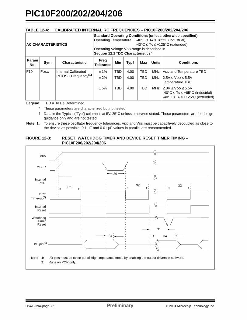
PIC10F200/202/204/206
TABLE 12-4: CALIBRATED INTERNAL RC FREQUENCIES – PIC10F200/202/204/206
FIGURE 12-3: RESET, WATCHDOG TIMER AND DEVICE RESET TIMER TIMING – PIC10F200/202/204/206
AC CHARACTERISTICS
Standard Operating Conditions (unless otherwise specified)Operating Temperature -40°C ≤ TA ≤ +85°C (industrial),
-40°C ≤ TA ≤ +125°C (extended)Operating Voltage VDD range is described inSection 12.1 “DC Characteristics”.
Param No.
Sym CharacteristicFreq
ToleranceMin Typ† Max Units Conditions
F10 FOSC Internal Calibrated INTOSC Frequency(1)
± 1% TBD 4.00 TBD MHz VDD and Temperature TBD
± 2% TBD 4.00 TBD MHz 2.5V ≤ VDD ≤ 5.5VTemperature TBD
± 5% TBD 4.00 TBD MHz 2.0V ≤ VDD ≤ 5.5V-40°C ≤ TA ≤ +85°C (industrial)-40°C ≤ TA ≤ +125°C (extended)
Legend: TBD = To Be Determined.
* These parameters are characterized but not tested.† Data in the Typical (“Typ”) column is at 5V, 25°C unless otherwise stated. These parameters are for design
guidance only and are not tested.Note 1: To ensure these oscillator frequency tolerances, VDD and VSS must be capacitively decoupled as close to
the device as possible. 0.1 µF and 0.01 µF values in parallel are recommended.
VDD
MCLR
InternalPOR
DRTTimeout(2)
InternalReset
WatchdogTimerReset
32
31
34
I/O pin(1)
32 32
34
30
Note 1: I/O pins must be taken out of High-impedance mode by enabling the output drivers in software.2: Runs on POR only.
DS41239A-page 72 Preliminary 2004 Microchip Technology Inc.

PIC10F200/202/204/206
TABLE 12-5: RESET, WATCHDOG TIMER AND DEVICE RESET TIMER – PIC10F200/202/204/206
FIGURE 12-4: TIMER0 CLOCK TIMINGS – PIC10F200/202/204/206
TABLE 12-6: TIMER0 CLOCK REQUIREMENTS – PIC10F200/202/204/206
AC CHARACTERISTICS
Standard Operating Conditions (unless otherwise specified)Operating Temperature -40°C ≤ TA ≤ +85°C (industrial)
-40°C ≤ TA ≤ +125°C (extended)Operating Voltage VDD range is described in Section 12.1 “DC Characteristics”
ParamNo.
Sym Characteristic Min Typ(1) Max Units Conditions
30 TMCL MCLR Pulse Width (low) 2000* — — ns VDD = 5.0V
31 TWDT Watchdog Timer Time-out Period (no prescaler)
9*9*
18*18*
30*40*
msms
VDD = 5.0V (Industrial)VDD = 5.0V (Extended)
32 TDRT Device Reset Timer Period(2) 9*9*
18*18*
30*40*
msms
VDD = 5.0V (Industrial)VDD = 5.0V (Extended)
34 TIOZ I/O High-impedance from MCLR low
— — 2000* ns
* These parameters are characterized but not tested.Note 1: Data in the Typical (“Typ”) column is at 5V, 25°C unless otherwise stated. These parameters are for design
guidance only and are not tested.
AC CHARACTERISTICS
Standard Operating Conditions (unless otherwise specified)Operating Temperature -40°C ≤ TA ≤ +85°C (industrial)
-40°C ≤ TA ≤ +125°C (extended)Operating Voltage VDD range is described inSection 12.1 “DC Characteristics”.
Param No.
Sym Characteristic Min Typ(1) Max Units Conditions
40 Tt0H T0CKI High Pulse Width
No Prescaler 0.5 TCY + 20* — — nsWith Prescaler 10* — — ns
41 Tt0L T0CKI Low Pulse Width
No Prescaler 0.5 TCY + 20* — — nsWith Prescaler 10* — — ns
42 Tt0P T0CKI Period 20 or TCY + 40* N — — ns Whichever is greater.N = Prescale Value(1, 2, 4,..., 256)
* These parameters are characterized but not tested.Note 1: Data in the Typical (“Typ”) column is at 5V, 25°C unless otherwise stated. These parameters are for design
guidance only and are not tested.
T0CKI
40 41
42
2004 Microchip Technology Inc. Preliminary DS41239A-page 73

PIC10F200/202/204/206
NOTES:
DS41239A-page 74 Preliminary 2004 Microchip Technology Inc.

PIC10F200/202/204/206
13.0 DC AND AC CHARACTERISTICS GRAPHS AND CHARTS
Graphs and charts are not available at this time.
2004 Microchip Technology Inc. Preliminary DS41239A-page 75

PIC10F200/202/204/206
NOTES:
DS41239A-page 76 Preliminary 2004 Microchip Technology Inc.

PIC10F200/202/204/206
14.0 PACKAGING INFORMATION
14.1 Package Marking Information
XXXXXXXXXXXXXNNN
YYWW
8-Lead PDIP (300 mil) Example10F206-I
0432/P017
6-Lead SOT-23
X X N NExampleCH17
Legend: XX...X Customer specific information*Y Year code (last digit of calendar year)YY Year code (last 2 digits of calendar year)WW Week code (week of January 1 is week ‘01’)NNN Alphanumeric traceability code
Note: In the event the full Microchip part number cannot be marked on one line, it willbe carried over to the next line thus limiting the number of available charactersfor customer specific information.
* Standard PICmicro device marking consists of Microchip part number, year code, week code, andtraceability code. For PICmicro device marking beyond this, certain price adders apply. Please checkwith your Microchip Sales Office. For QTP devices, any special marking adders are included in QTPprice.
2004 Microchip Technology Inc. Preliminary DS41239A-page 77

PIC10F200/202/204/206
6-Lead Plastic Small Outline Transistor (CH or OT) (SOT-23)
10501050βMold Draft Angle Bottom
10501050αMold Draft Angle Top
0.500.430.35.020.017.014BLead Width
0.200.150.09.008.006.004cLead Thickness
10501050φFoot Angle
0.550.450.35.022.018.014LFoot Length
3.102.952.80.122.116.110DOverall Length
1.751.631.50.069.064.059E1Molded Package Width
3.002.802.60.118.110.102EOverall Width
0.150.080.00.006.003.000A1Standoff
1.301.100.90.051.043.035A2Molded Package Thickness
1.451.180.90.057.046.035AOverall Height
1.90.075p1Outside lead pitch (basic)
0.95.038pPitch
66nNumber of Pins
MAXNOMMINMAXNOMMINDimension Limits
MILLIMETERSINCHES*Units
1
DB
n
E
E1
L
c
β
φ
α
A2A
A1
p1
exceed .005" (0.127mm) per side.
Dimensions D and E1 do not include mold flash or protrusions. Mold flash or protrusions shall not
Notes:
JEITA (formerly EIAJ) equivalent: SC-74A
Drawing No. C04-120
*Controlling Parameter
DS41239A-page 78 Preliminary 2004 Microchip Technology Inc.
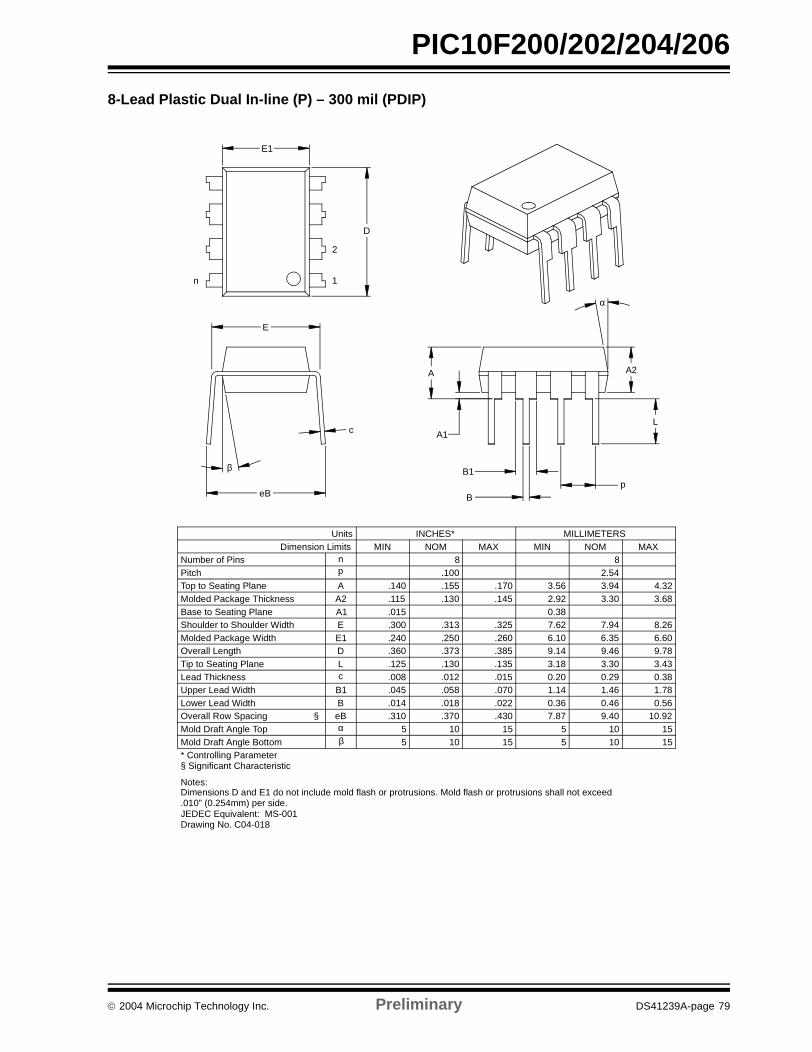
PIC10F200/202/204/206
8-Lead Plastic Dual In-line (P) – 300 mil (PDIP)
B1
B
A1
A
L
A2
p
α
E
eB
β
c
E1
n
D
1
2
Units INCHES* MILLIMETERSDimension Limits MIN NOM MAX MIN NOM MAX
Number of Pins n 8 8Pitch p .100 2.54Top to Seating Plane A .140 .155 .170 3.56 3.94 4.32Molded Package Thickness A2 .115 .130 .145 2.92 3.30 3.68Base to Seating Plane A1 .015 0.38Shoulder to Shoulder Width E .300 .313 .325 7.62 7.94 8.26Molded Package Width E1 .240 .250 .260 6.10 6.35 6.60Overall Length D .360 .373 .385 9.14 9.46 9.78Tip to Seating Plane L .125 .130 .135 3.18 3.30 3.43Lead Thickness c .008 .012 .015 0.20 0.29 0.38Upper Lead Width B1 .045 .058 .070 1.14 1.46 1.78Lower Lead Width B .014 .018 .022 0.36 0.46 0.56Overall Row Spacing § eB .310 .370 .430 7.87 9.40 10.92Mold Draft Angle Top α 5 10 15 5 10 15Mold Draft Angle Bottom β 5 10 15 5 10 15* Controlling Parameter
Notes:Dimensions D and E1 do not include mold flash or protrusions. Mold flash or protrusions shall not exceed
JEDEC Equivalent: MS-001Drawing No. C04-018
.010” (0.254mm) per side.
§ Significant Characteristic
2004 Microchip Technology Inc. Preliminary DS41239A-page 79

PIC10F200/202/204/206
NOTES:
DS41239A-page 80 Preliminary 2004 Microchip Technology Inc.

PIC10F200/202/204/206
INDEX
AALU ....................................................................................... 9Assembler
MPASM Assembler..................................................... 59
BBlock Diagram
On-Chip Reset Circuit ................................................. 44Timer0................................................................... 29, 33TMR0/WDT Prescaler..................................... 32, 36, 38Watchdog Timer.......................................................... 47
Brown-Out Protection Circuit .............................................. 48
CC Compilers
MPLAB C17 ................................................................ 60MPLAB C18 ................................................................ 60MPLAB C30 ................................................................ 60
Carry ..................................................................................... 9Clocking Scheme ................................................................ 13Code Protection ............................................................ 41, 50Comparator
Comparator Module .................................................... 37Configuration............................................................... 38Interrupts..................................................................... 39Operation .................................................................... 39Reference ................................................................... 39
Configuration Bits................................................................ 41
DDC and AC Characteristics ................................................. 75Demonstration Boards
PICDEM 1 ................................................................... 62PICDEM 17 ................................................................. 63PICDEM 18R .............................................................. 63PICDEM 2 Plus ........................................................... 62PICDEM 3 ................................................................... 62PICDEM 4 ................................................................... 62PICDEM LIN ............................................................... 63PICDEM USB.............................................................. 63PICDEM.net Internet/Ethernet .................................... 62
Development Support ......................................................... 59Digit Carry ............................................................................. 9
EErrata .................................................................................... 3Evaluation and Programming Tools .................................... 63
FFamily of Devices
PIC10F200/202/204/206............................................... 5
GGPIO ................................................................................... 25
II/O Interfacing ..................................................................... 25I/O Ports ............................................................................. 25I/O Programming Considerations ....................................... 26ID Locations.................................................................. 41, 50INDF ................................................................................... 23Indirect Data Addressing .................................................... 23Instruction Cycle ................................................................. 13Instruction Flow/Pipelining.................................................. 13Instruction Set Summary .................................................... 52
LLoading of PC..................................................................... 22
MMemory Organization ......................................................... 15
Data Memory .............................................................. 16Program Memory (PIC10F200/204) ........................... 15Program Memory (PIC10F202/206) ........................... 16
MPLAB ASM30 Assembler, Linker, Librarian ..................... 60MPLAB ICD 2 In-Circuit Debugger ..................................... 61MPLAB ICE 2000 High-Performance Universal
In-Circuit Emulator..................................................... 61MPLAB ICE 4000 High-Performance Universal
In-Circuit Emulator..................................................... 61MPLAB Integrated Development Environment Software.... 59MPLAB PM3 Device Programmer ...................................... 61MPLINK Object Linker/MPLIB Object Librarian .................. 60
OOption Register................................................................... 20OSCCAL Register............................................................... 21Oscillator Configurations..................................................... 42Oscillator Types
HS............................................................................... 42LP ............................................................................... 42
PPIC10F200/202/204/206 Device Varieties............................ 7PICkit 1 Flash Starter Kit .................................................... 63PICSTART Plus Development Programmer....................... 62POR
Device Reset Timer (DRT) ................................... 41, 46PD............................................................................... 48Power-on Reset (POR)............................................... 41TO............................................................................... 48
Power-down Mode.............................................................. 49Prescaler ...................................................................... 31, 35PRO MATE II Universal Device Programmer ..................... 61Program Counter ................................................................ 22
QQ cycles .............................................................................. 13
RRead-Modify-Write.............................................................. 26Register File Map
PIC10F200/204 .......................................................... 17PIC10F202/206 .......................................................... 17
RegistersSpecial Function ......................................................... 18
Reset .................................................................................. 41Reset on Brown-Out ........................................................... 48
2004 Microchip Technology Inc. Preliminary DS41239A-page 81

PIC10F200/202/204/206
SSleep ............................................................................. 41, 49Software Simulator (MPLAB SIM)....................................... 60Software Simulator (MPLAB SIM30)................................... 60Special Features of the CPU............................................... 41Special Function Registers ................................................. 18Stack ................................................................................... 22Status Register................................................................ 9, 19
TTimer0
Timer0................................................................... 29, 33Timer0 (TMR0) Module ......................................... 29, 33TMR0 with External Clock..................................... 30, 34
Timing Parameter Symbology and Load Conditions........... 71TRIS Registers.................................................................... 25
WWake-up from Sleep ........................................................... 49Watchdog Timer (WDT) ................................................ 41, 46
Period.......................................................................... 46Programming Considerations ..................................... 46
WWW, On-Line Support........................................................ 3
ZZero bit .................................................................................. 9
DS41239A-page 82 Preliminary 2004 Microchip Technology Inc.

PIC10F200/202/204/206
ON-LINE SUPPORT
Microchip provides on-line support on the MicrochipWorld Wide Web site.
The web site is used by Microchip as a means to makefiles and information easily available to customers. Toview the site, the user must have access to the Internetand a web browser, such as Netscape® or Microsoft®
Internet Explorer. Files are also available for FTPdownload from our FTP site.
Connecting to the Microchip Internet Web Site
The Microchip web site is available at the followingURL:
www.microchip.com
The file transfer site is available by using an FTPservice to connect to:
ftp://ftp.microchip.com
The web site and file transfer site provide a variety ofservices. Users may download files for the latestDevelopment Tools, Data Sheets, Application Notes,User’s Guides, Articles and Sample Programs. A vari-ety of Microchip specific business information is alsoavailable, including listings of Microchip sales offices,distributors and factory representatives. Other dataavailable for consideration is:
• Latest Microchip Press Releases• Technical Support Section with Frequently Asked
Questions • Design Tips
• Device Errata• Job Postings• Microchip Consultant Program Member Listing
• Links to other useful web sites related to Microchip Products
• Conferences for products, Development Systems, technical information and more
• Listing of seminars and events
SYSTEMS INFORMATION AND UPGRADE HOT LINE
The Systems Information and Upgrade Line providessystem users a listing of the latest versions of all ofMicrochip’s development systems software products.Plus, this line provides information on how customerscan receive the most current upgrade kits. The Hot LineNumbers are:
1-800-755-2345 for U.S. and most of Canada, and
1-480-792-7302 for the rest of the world.
042003
2004 Microchip Technology Inc. Preliminary DS41239A-page 83

PIC10F200/202/204/206
READER RESPONSE
It is our intention to provide you with the best documentation possible to ensure successful use of your Microchip prod-uct. If you wish to provide your comments on organization, clarity, subject matter, and ways in which our documentationcan better serve you, please FAX your comments to the Technical Publications Manager at (480) 792-4150.
Please list the following information, and use this outline to provide us with your comments about this document.
To: Technical Publications Manager
RE: Reader Response
Total Pages Sent ________
From: Name
Company
Address
City / State / ZIP / Country
Telephone: (_______) _________ - _________
Application (optional):
Would you like a reply? Y N
Device: Literature Number:
Questions:
FAX: (______) _________ - _________
DS41239APIC10F200/202/204/206
1. What are the best features of this document?
2. How does this document meet your hardware and software development needs?
3. Do you find the organization of this document easy to follow? If not, why?
4. What additions to the document do you think would enhance the structure and subject?
5. What deletions from the document could be made without affecting the overall usefulness?
6. Is there any incorrect or misleading information (what and where)?
7. How would you improve this document?
DS41239A-page 84 Preliminary 2004 Microchip Technology Inc.

2004 Microchip Technology Inc. Preliminary DS41239A-page 85
PIC10F200/202/204/206
PRODUCT IDENTIFICATION SYSTEM
To order or obtain information, e.g., on pricing or delivery, refer to the factory or the listed sales office.
PART NO. X /XX XXX
PatternPackageTemperatureRange
Device
Device PIC10F200PIC10F202PIC10F204PIC10F206PIC10F200T (Tape & Reel)PIC10F202T (Tape & Reel)PIC10F204T (Tape & Reel)PIC10F206T (Tape & Reel)
Temperature Range I = -40°C to +85°C (Industrial)E = -40°C to +125°C (Extended)
Package PG = 300 mil PDIP (Pb-free)OTG = SOT-23, 6-LD (Pb-free)
Pattern Special Requirements
Examples:
a) PIC10F200-I/PG = Industrial temp., PDIPpackage (Pb-free)
b) PIC10F202T-E/OTG = Extended temp., SOT-23 package (Pb-free), Tape and Reel
Note: Tape and Reel available for only the following packages: SOT-23.

DS41239A-page 86 Preliminary 2004 Microchip Technology Inc.
AMERICASCorporate Office2355 West Chandler Blvd.Chandler, AZ 85224-6199Tel: 480-792-7200 Fax: 480-792-7277Technical Support: 480-792-7627Web Address: www.microchip.com
Atlanta3780 Mansell Road, Suite 130Alpharetta, GA 30022Tel: 770-640-0034 Fax: 770-640-0307
Boston2 Lan Drive, Suite 120Westford, MA 01886Tel: 978-692-3848 Fax: 978-692-3821
Chicago333 Pierce Road, Suite 180Itasca, IL 60143Tel: 630-285-0071 Fax: 630-285-0075
Dallas4570 Westgrove Drive, Suite 160Addison, TX 75001Tel: 972-818-7423 Fax: 972-818-2924
DetroitTri-Atria Office Building 32255 Northwestern Highway, Suite 190Farmington Hills, MI 48334Tel: 248-538-2250Fax: 248-538-2260
Kokomo2767 S. Albright Road Kokomo, IN 46902Tel: 765-864-8360Fax: 765-864-8387
Los Angeles18201 Von Karman, Suite 1090Irvine, CA 92612Tel: 949-263-1888 Fax: 949-263-1338
San Jose1300 Terra Bella AvenueMountain View, CA 94043Tel: 650-215-1444Fax: 650-961-0286
Toronto6285 Northam Drive, Suite 108Mississauga, Ontario L4V 1X5, CanadaTel: 905-673-0699 Fax: 905-673-6509
ASIA/PACIFICAustraliaSuite 22, 41 Rawson StreetEpping 2121, NSWAustraliaTel: 61-2-9868-6733 Fax: 61-2-9868-6755
China - BeijingUnit 706BWan Tai Bei Hai Bldg.No. 6 Chaoyangmen Bei Str. Beijing, 100027, ChinaTel: 86-10-85282100 Fax: 86-10-85282104China - ChengduRm. 2401-2402, 24th Floor, Ming Xing Financial TowerNo. 88 TIDU StreetChengdu 610016, ChinaTel: 86-28-86766200 Fax: 86-28-86766599China - FuzhouUnit 28F, World Trade PlazaNo. 71 Wusi RoadFuzhou 350001, ChinaTel: 86-591-7503506 Fax: 86-591-7503521China - Hong Kong SARUnit 901-6, Tower 2, Metroplaza223 Hing Fong RoadKwai Fong, N.T., Hong KongTel: 852-2401-1200 Fax: 852-2401-3431China - ShanghaiRoom 701, Bldg. BFar East International PlazaNo. 317 Xian Xia RoadShanghai, 200051Tel: 86-21-6275-5700 Fax: 86-21-6275-5060China - ShenzhenRm. 1812, 18/F, Building A, United PlazaNo. 5022 Binhe Road, Futian DistrictShenzhen 518033, ChinaTel: 86-755-82901380 Fax: 86-755-8295-1393China - ShundeRoom 401, Hongjian Building, No. 2 Fengxiangnan Road, Ronggui Town, ShundeDistrict, Foshan City, Guangdong 528303, ChinaTel: 86-757-28395507 Fax: 86-757-28395571China - QingdaoRm. B505A, Fullhope Plaza,No. 12 Hong Kong Central Rd.Qingdao 266071, ChinaTel: 86-532-5027355 Fax: 86-532-5027205IndiaDivyasree Chambers1 Floor, Wing A (A3/A4)No. 11, O’Shaugnessey RoadBangalore, 560 025, IndiaTel: 91-80-22290061 Fax: 91-80-22290062JapanBenex S-1 6F3-18-20, ShinyokohamaKohoku-Ku, Yokohama-shiKanagawa, 222-0033, JapanTel: 81-45-471- 6166 Fax: 81-45-471-6122
Korea168-1, Youngbo Bldg. 3 FloorSamsung-Dong, Kangnam-KuSeoul, Korea 135-882Tel: 82-2-554-7200 Fax: 82-2-558-5932 or 82-2-558-5934Singapore200 Middle Road#07-02 Prime CentreSingapore, 188980Tel: 65-6334-8870 Fax: 65-6334-8850TaiwanKaohsiung Branch30F - 1 No. 8Min Chuan 2nd RoadKaohsiung 806, TaiwanTel: 886-7-536-4818Fax: 886-7-536-4803TaiwanTaiwan Branch11F-3, No. 207Tung Hua North RoadTaipei, 105, TaiwanTel: 886-2-2717-7175 Fax: 886-2-2545-0139
EUROPEAustriaDurisolstrasse 2A-4600 WelsAustriaTel: 43-7242-2244-399Fax: 43-7242-2244-393DenmarkRegus Business CentreLautrup hoj 1-3Ballerup DK-2750 DenmarkTel: 45-4420-9895 Fax: 45-4420-9910FranceParc d’Activite du Moulin de Massy43 Rue du Saule TrapuBatiment A - ler Etage91300 Massy, FranceTel: 33-1-69-53-63-20 Fax: 33-1-69-30-90-79GermanySteinheilstrasse 10D-85737 Ismaning, GermanyTel: 49-89-627-144-0 Fax: 49-89-627-144-44ItalyVia Quasimodo, 1220025 Legnano (MI)Milan, Italy Tel: 39-0331-742611 Fax: 39-0331-466781NetherlandsWaegenburghtplein 4NL-5152 JR, Drunen, NetherlandsTel: 31-416-690399 Fax: 31-416-690340United Kingdom505 Eskdale RoadWinnersh TriangleWokingham Berkshire, England RG41 5TUTel: 44-118-921-5869Fax: 44-118-921-5820
05/28/04
WORLDWIDE SALES AND SERVICE