pic16(l)f170x/171x product brief - markit · pic16(l)f170x/171x ds40001708a-page 4 advance...
TRANSCRIPT
PIC16(L)F170X/171XCost Effective 8-Bit Intelligent Analog Flash Microcontrollers
Description:PIC16F(L)170X/171X microcontrollers combine Intelligent Analog integration with low cost and extreme low power (XLP) tosuit a variety of general purpose applications. These 14 to 44-pin devices deliver on-chip Op Amps, Core IndependentPeripherals (CLC, NCO and COG), Peripheral Pin Select and Zero-Cross Detect, providing for increased design flexibility.
Core Features:• C Compiler Optimized RISC Architecture• Only 49 Instructions• Operating Speed:
- 0-32 MHz clock input- 125 ns minimum instruction cycle
• Interrupt Capability• 16-Level Deep Hardware Stack• Up to Four 8-bit Timers• One 16-bit Timer• Power-on Reset (POR)• Power-up Timer (PWRT)• Low-Power Brown-Out Reset (LPBOR)• Programmable Watchdog Timer (WDT) up to 256s• Programmable Code Protection
Memory:• Up to 16 Kwords Flash Program Memory• Up to 2048 Bytes Data SRAM Memory• Direct, Indirect and Relative Addressing modes
Operating Characteristics:• Operating Voltage Range:
- 1.8V to 3.6V (PIC16LF170X/171X)- 2.3V to 5.5V (PIC16F170X/171X)
• Temperature Range:- Industrial: -40°C to 85°C- Extended: -40°C to 125°C
eXtreme Low-Power (XLP) Features:• Sleep mode: 50 nA @ 1.8V, typical• Watchdog Timer: 500 nA @ 1.8V, typical• Secondary Oscillator: 500 nA @ 32 kHz• Operating Current: - 8 uA @ 32 kHz, 1.8V, typical - 32 uA/MHz @ 1.8V, typical
Digital Peripherals:• Configurable Logic Cell (CLC):
- Integrated combinational and sequential logic• Complementary Output Generator (COG):
- Rising/falling edge dead-band control/blanking• Numerically Controlled Oscillator (NCO):
- Generates true linear frequency control and increased frequency resolution
- Input Clock: 0Hz < FNCO < 32 MHz- Resolution: FNCO/220
• Capture/Compare/PWM (CCP) module• PWM: Two 10-bit Pulse-Width Modulators• Serial Communications:
- SPI, I2C™, RS-232, RS-485, LIN compatible- Auto-Baud Detect, auto-wake-up on start
• Up to 35 I/O Pins and One Input Pin:- Individually programmable pull-ups- Slew rate control- Interrupt-on-change with edge-select
• Peripheral Pin Select (PPS):- Enables pin mapping of digital I/O
Intelligent Analog Peripherals:• Operational Amplifiers:
- Two configurable rail-to-rail op amps- Selectable internal and external channels- 2 MHz gain bandwidth product
• High-Speed Comparators:- Up to two comparators- 50 ns response time- Rail-to-rail inputs
• 10-Bit Analog-to-Digital Converter (ADC):- Up to 28 external channels- Conversion available during Sleep- Temperature indicator
• Zero-Cross Detector (ZCD):- Detect when AC signal on pin crosses ground
• 8-Bit Digital-to-Analog Converter (DAC):- Output available externally- Internal connections to comparators, op amps,
Fixed Voltage Reference (FVR) and ADC• Internal Voltage Reference module
2013 Microchip Technology Inc. Advance Information DS40001708A-page 1

PIC16(L)F170X/171X
Clocking Structure:• 16 MHz Internal Oscillator Block:- ±1% at calibration- Selectable frequency range from 0 to 32 MHz
• 31 kHz Low-Power Internal Oscillator• External Oscillator Block with:
- Three crystal/resonator modes up to 20 MHz- Two external clock modes up to 32 MHz
• Fail-Safe Clock Monitor• Two-Speed Oscillator Start-up• Oscillator Start-up Timer (OST)
Programming/Debug Features:• In-Circuit Debug Integrated On-Chip• Emulation Header for Advanced Debug:
- Provides trace, background debug and up to 32 hardware break points
• In-Circuit Serial Programming™ (ICSP™) via Two Pins
PIC16(L)F170X/171X FAMILY TYPES
PACKAGES
Device
Prog
ram
Mem
ory
Flas
h (w
ords
)
Dat
a SR
AM
(byt
es)
I/O P
ins
8-bi
t/16-
bit T
imer
s
Hig
h-Sp
eed
Com
para
tors
Op
Am
p
10-b
it A
DC
(ch)
5-/8
-bit
DA
C
Zero
Cro
ss
CC
P/PW
M
CO
G
EUSA
RT
I2 C™
/SPI
CLC
NC
O
Deb
ug(1
)
PIC16(L)F1703 2k 256 12 2/1 0 2 8 0/0 1 2/0 0 0 1 0 0 I/EPIC16(L)F1704 4k 512 12 4/1 2 2 8 0/1 1 2/2 1 1 1 3 0 I/EPIC16(L)F1705 8k 1024 12 4/1 2 2 8 0/1 1 2/2 1 1 1 3 0 I/EPIC16(L)F1707 2k 256 18 2/1 0 2 8 0/0 1 2/0 0 0 1 0 0 I/EPIC16(L)F1708 4k 512 18 4/1 2 2 12 0/1 1 2/2 1 1 1 3 0 I/EPIC16(L)F1709 8k 1024 18 4/1 2 2 12 0/1 1 2/2 1 1 1 3 0 I/EPIC16(L)F1713 4k 512 25 4/1 2 2 17 1/1 1 2/2 1 1 1 4 1 I/EPIC16(L)F1716 8k 1024 25 4/1 2 2 17 1/1 1 2/2 1 1 1 4 1 I/EPIC16(L)F1717 8k 1024 36 4/1 2 2 28 1/1 1 2/2 1 1 1 4 1 I/EPIC16(L)F1718 16k 2048 25 4/1 2 2 17 1/1 1 2/2 1 1 1 4 1 I/EPIC16(L)F1719 16k 2048 36 4/1 2 2 28 1/1 1 2/2 1 1 1 4 1 I/ENote 1: I – Debugging integrated on chip; H – Debugging via ICD header; E – Debugging via Emulation header.
Device PDIP TSSOP QFN(4x4x0.9) SOIC SSOP SPDIP QFN
(6x6x0.9)UQFN
(4x4x0.5) TQFP UQFN(5x5x0.5)
PIC16F1703 x x x xPIC16F1704 x x x xPIC16F1705 x x x xPIC16F1707 x x x xPIC16F1708 x x x xPIC16F1709 x x x xPIC16F1713 x x x x xPIC16F1716 x x x x xPIC16F1717 x x xPIC16F1718 x x x x xPIC16F1719 x x x
DS40001708A-page 2 Advance Information 2013 Microchip Technology Inc.
PIC16(L)F170X/171X
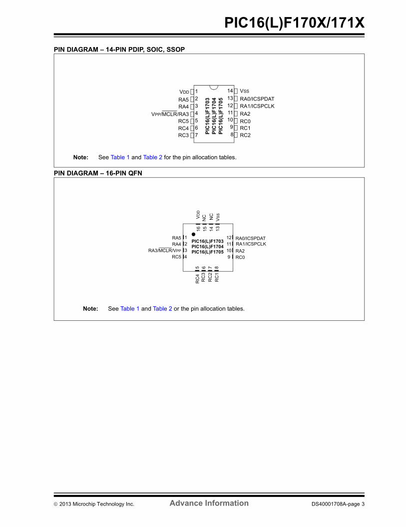
PIN DIAGRAM – 14-PIN PDIP, SOIC, SSOPPIN DIAGRAM – 16-PIN QFN
PIC
16(L
)F17
03PI
C16
(L)F
1704
PIC
16(L
)F17
05
1234567
VDD
RA5RA4
VPP/MCLR/RA3RC5RC4RC3
RA0/ICSPDATRA1/ICSPCLKRA2RC0RC1RC2
1413121110
98
VSS
Note: See Table 1 and Table 2 for the pin allocation tables.
23
1
9101112
RC
4
4
VS
S
RA0/ICSPDATRA1/ICSPCLKRA2RC0
NC
NCV
DD
RA5RA4
RA3/MCLR/VPP
RC5
RC
3R
C2
RC
1
6 75 8
15 1416 13
PIC16(L)F1703PIC16(L)F1704PIC16(L)F1705
Note: See Table 1 and Table 2 or the pin allocation tables.
2013 Microchip Technology Inc. Advance Information DS40001708A-page 3
PIC16(L)F170X/171X
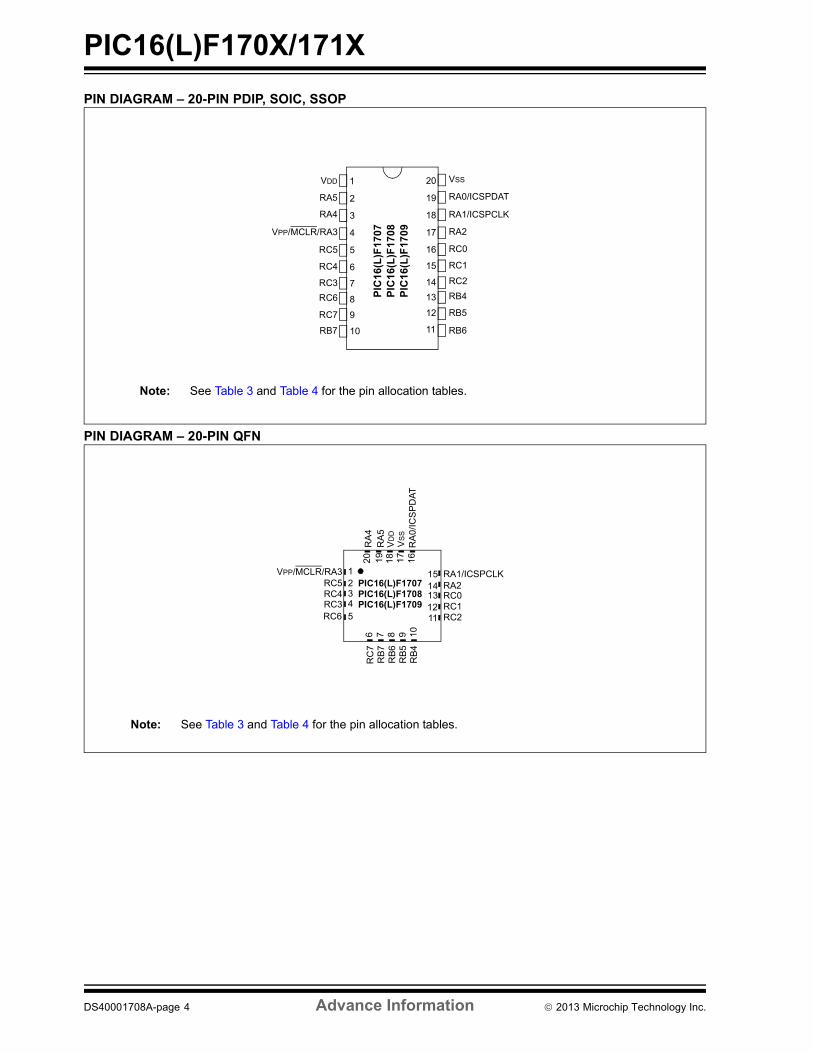
PIN DIAGRAM – 20-PIN PDIP, SOIC, SSOPPIN DIAGRAM – 20-PIN QFN
PIC
16(L
)F17
07PI
C16
(L)F
1708
PIC
16(L
)F17
09
2
3
4
5
6
7
8
9
10
VDD
RA5
RA4
VPP/MCLR/RA3
RC5
RC4
RC3RC6
RC7
RB7
RA0/ICSPDAT
RA1/ICSPCLK
RA2
RC0
RC1
RC2RB4
RB5
RB6
20
19
18
17
16
15
1413
12
11
VSS1
Note: See Table 3 and Table 4 for the pin allocation tables.
2345
1
6 7 8 9
20 19 18 17 1610
12131415
11
PIC16(L)F1707PIC16(L)F1708PIC16(L)F1709
RB4
RB5
RB6
RB7
RC
7
VPP/MCLR/RA3RC5RC4RC3RC6
RA
4R
A5
VD
DV
SS
RA
0/IC
SP
DAT
RA1/ICSPCLKRA2RC0RC1RC2
Note: See Table 3 and Table 4 for the pin allocation tables.
DS40001708A-page 4 Advance Information 2013 Microchip Technology Inc.
PIC16(L)F170X/171X
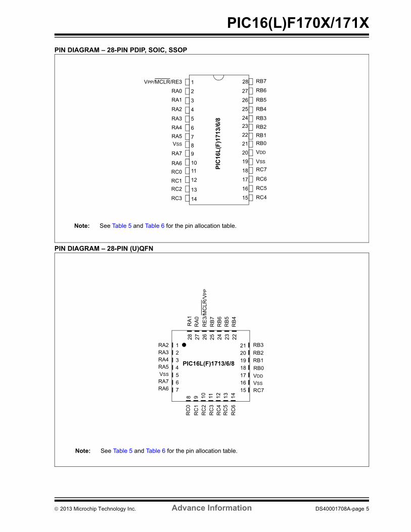
PIN DIAGRAM – 28-PIN PDIP, SOIC, SSOPPIN DIAGRAM – 28-PIN (U)QFN
PIC
16L(
F)17
13/6
/8
1
2
3
4
5
6
789
10
VPP/MCLR/RE3
RA0
RA1
RA2
RA3
RA4RA5
RB6
RB5
RB4
RB3RB2RB1RB0
VDD
VSS
11
12
13
14 15
16
17
18
1920
28
27
26
25
2423
22
21VSS
RA7
RA6RC0
RC1RC2
RC3
RC5
RC4
RC7
RC6
RB7
Note: See Table 5 and Table 6 for the pin allocation table.
23
6
1
18192021
1571617
RC
0
54
RB
7R
B6
RB
5R
B4
RB0VDD
VSS
RC7
RC
6R
C5
RC
4
RE
3/M
CLR
/VP
P
RA
0R
A1
RA2RA3RA4RA5VSS
RA7RA6
RC
1R
C2
RC
3
9 10 138 141211
27 26 2328 222425
PIC16L(F)1713/6/8
RB3RB2RB1
Note: See Table 5 and Table 6 for the pin allocation table.
2013 Microchip Technology Inc. Advance Information DS40001708A-page 5

PIC16(L)F170X/171X
PIN DIAGRAM – 40-PIN PDIPPIC
16L(
F)17
17/9
2
3
4
5
6
789
10
VPP/MCLR/RE3
RA0RA1
RA2
RA3
RA4RA5RE0
RE1RE2
RB6/ICSPCLK
RB5
RB4
RB0
VDD
VSS
RD2
11
12
13
14
15
16
1718
19
20
40
39
38
37
36
35
343332
3130
29
28
27
26
25
2423
22
21
VDD
VSS
RA7
RA6RC0
RC1
RC2RC3RD0
RD1
RC5RC4RD3
RD4
RC7
RC6
RD7
RD6
RD5
RB7/ICSPDAT1
RB3
RB2RB1
Note: See Table 7 and Table 8 for the pin allocation table.
DS40001708A-page 6 Advance Information 2013 Microchip Technology Inc.
PIC16(L)F170X/171X
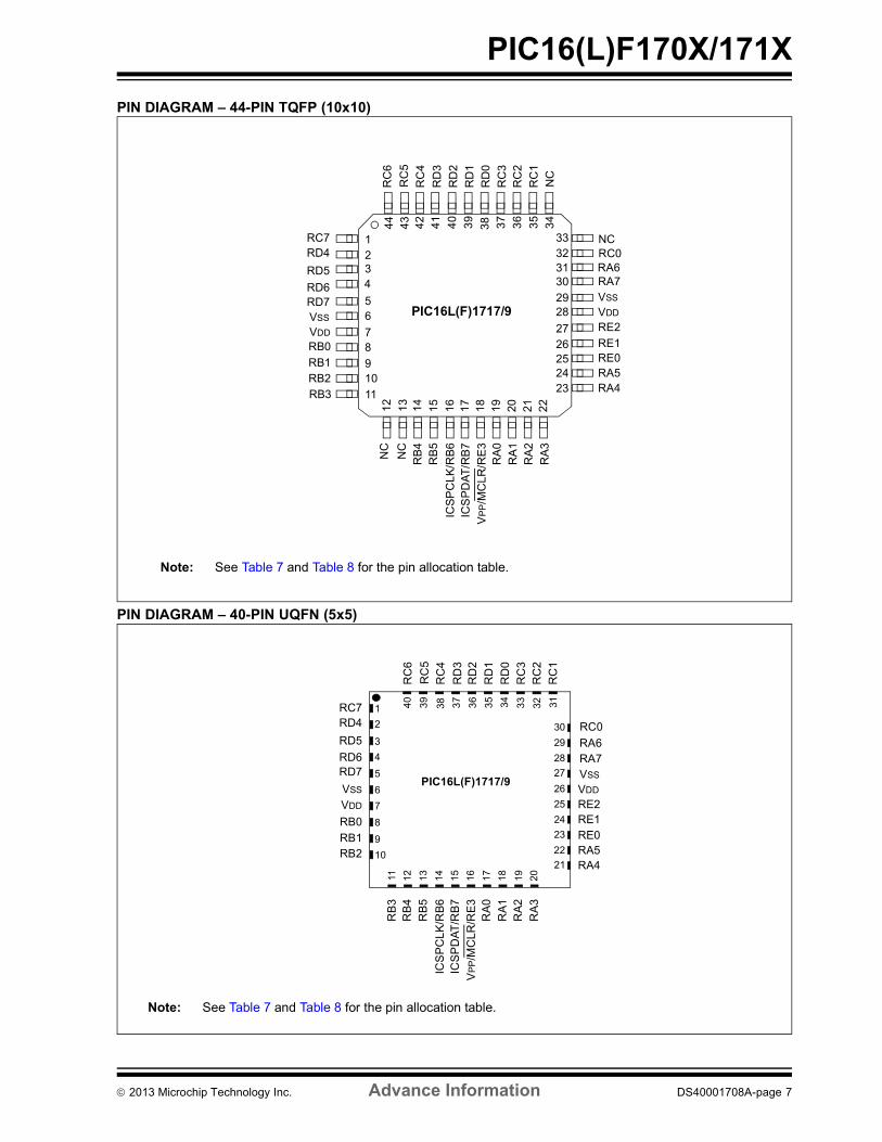
PIN DIAGRAM – 44-PIN TQFP (10x10)PIN DIAGRAM – 40-PIN UQFN (5x5)
1011
23
6
1
18 19 20 21 2212 13 14 15
38
87
44 43 42 41 40 3916 17
2930313233
232425262728
36 3435
9
37
54
PIC16L(F)1717/9
RC
6R
C5
RC
4R
D3
RD
2R
D1
RD
0R
C3
RC
2R
C1
RC0
RA
1R
A0
VPP
/MC
LR/R
E3
RB3
ICS
PD
AT/R
B7
ICS
PC
LK/R
B6
RB
5R
B4
NC
RA
3R
A2
RC7RD4RD5RD6RD7VSSVDDRB0RB1RB2
RA6RA7VSS
NC
VDDRE2RE1RE0RA5RA4
NC
NC
Note: See Table 7 and Table 8 for the pin allocation table.
10
11
2
3456
1
18 19 20
2122
12 13 14 1538
87
40 39
16 17
2930
313233
232425262728
36 3435
9
37
RA
1R
A0
VPP
/MC
LR/R
E3
RB
3
ICS
PD
AT/R
B7
ICS
PC
LK/R
B6
RB
5R
B4
RC
6R
C5
RC
4R
D3
RD
2R
D1
RD
0R
C3
RC
2R
C1
RC0RA6RA7VSSVDDRE2RE1RE0RA5RA4
RC7RD4RD5RD6RD7VSS
VDD
RB0RB1RB2
PIC16L(F)1717/9
RA
3R
A2
Note: See Table 7 and Table 8 for the pin allocation table.
2013 Microchip Technology Inc. Advance Information DS40001708A-page 7
PIC16(L)F170X/171X
DS
40001708A-page 8
Advance Inform
ation
2013 Microchip Technology Inc.
Pull-
up
Bas
ic
Y ICSPDAT
Y ICSPCLK
Y —
Y MCLRVPP
Y CLKOUT
Y CLKIN
Y —
Y —
Y —
Y —
Y —
Y —
— VDD
— VSS
— —
— —
— —
rs.
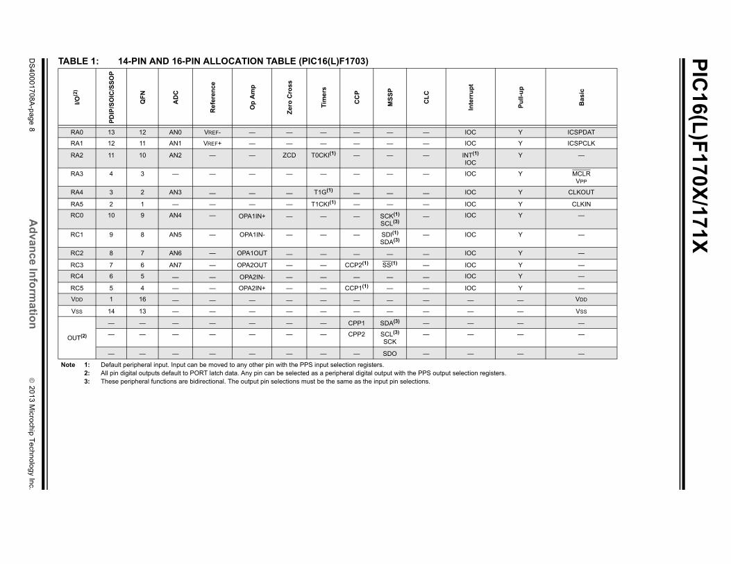
TABLE 1: 14-PIN AND 16-PIN ALLOCATION TABLE (PIC16(L)F1703)I/O
(2)
PDIP
/SO
IC/S
SOP
QFN
AD
C
Ref
eren
ce
Op
Am
p
Zero
Cro
ss
Tim
ers
CC
P
MSS
P
CLC
Inte
rrup
t
RA0 13 12 AN0 VREF- — — — — — — IOC
RA1 12 11 AN1 VREF+ — — — — — — IOC
RA2 11 10 AN2 — — ZCD T0CKI(1) — — — INT(1)
IOC
RA3 4 3 — — — — — — — — IOC
RA4 3 2 AN3 — — — T1G(1) — — — IOC
RA5 2 1 — — — — T1CKI(1) — — — IOC
RC0 10 9 AN4 — OPA1IN+ — — — SCK(1)
SCL(3)— IOC
RC1 9 8 AN5 — OPA1IN- — — — SDI(1)
SDA(3)— IOC
RC2 8 7 AN6 — OPA1OUT — — — — — IOC
RC3 7 6 AN7 — OPA2OUT — — CCP2(1) SS(1) — IOC
RC4 6 5 — — OPA2IN- — — — — — IOC
RC5 5 4 — — OPA2IN+ — — CCP1(1) — — IOC
VDD 1 16 — — — — — — — — —
VSS 14 13 — — — — — — — — —
OUT(2)
— — — — — — — CPP1 SDA(3) — —
— — — — — — — CPP2 SCL(3)
SCK— —
— — — — — — — — SDO — —
Note 1: Default peripheral input. Input can be moved to any other pin with the PPS input selection registers. 2: All pin digital outputs default to PORT latch data. Any pin can be selected as a peripheral digital output with the PPS output selection registe3: These peripheral functions are bidirectional. The output pin selections must be the same as the input pin selections.
2013 M
icrochip Technology Inc.A
dvance Information
DS
40001708A-page 9
PIC16(L)F170X/171X
TA
EUSA
RT
CLC
Inte
rrup
t
Pull-
up
Bas
ic
R — — IOC Y ICSPDAT
R — — IOC Y ICSPCLK
R — — INT(1)
IOCY —
R — — IOC Y MCLRVPP
R — — IOC Y CLKOUTOSC2
R — CLCIN3(1) IOC Y CLKINOSC1
R — — IOC Y —
R — CLCIN2(1) IOC Y —
R — — IOC Y —
R — CLCIN0(1) IOC Y —
R K(1) CLCIN1(1) IOC Y —
R X(3) — IOC Y —
V — — — — VDD
V — — — — VSS
O
CK CLC1OUT — — —
T(3) CLC2OUT — — —
TX CLC3OUT — — —
— — — — —
No
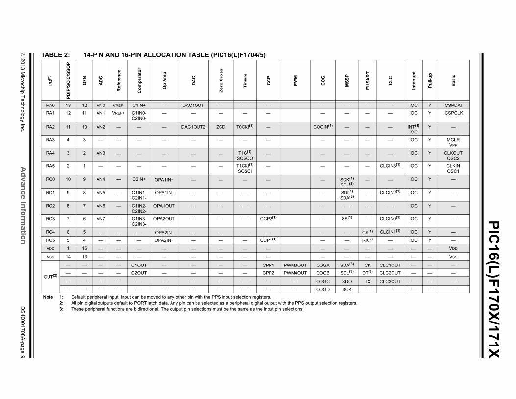
BLE 2: 14-PIN AND 16-PIN ALLOCATION TABLE (PIC16(L)F1704/5)I/O
(2)
PDIP
/SO
IC/S
SOP
QFN
AD
C
Ref
eren
ce
Com
para
tor
Op
Am
p
DA
C
Zero
Cro
ss
Tim
ers
CC
P
PWM
CO
G
MSS
P
A0 13 12 AN0 VREF- C1IN+ — DAC1OUT — — — — —
A1 12 11 AN1 VREF+ C1IN0-C2IN0-
— — — — — — —
A2 11 10 AN2 — — — DAC1OUT2 ZCD T0CKI(1) — COGIN(1) —
A3 4 3 — — — — — — — — — —
A4 3 2 AN3 — — — — — T1G(1)
SOSCO— — —
A5 2 1 — — — — — — T1CKI(1)
SOSCI— — —
C0 10 9 AN4 — C2IN+ OPA1IN+ — — — — — SCK(1)
SCL(3)
C1 9 8 AN5 — C1IN1-C2IN1-
OPA1IN- — — — — — SDI(1)
SDA(3)
C2 8 7 AN6 — C1IN2-C2IN2-
OPA1OUT — — — — — —
C3 7 6 AN7 — C1IN3-C2IN3-
OPA2OUT — — — CCP2(1) — SS(1)
C4 6 5 — — — OPA2IN- — — — — — — C
C5 5 4 — — — OPA2IN+ — — — CCP1(1) — — R
DD 1 16 — — — — — — — — — —
SS 14 13 — — — — — — — — — —
UT(2)
— — — — C1OUT — — — — CPP1 PWM3OUT COGA SDA(3)
— — — — C2OUT — — — — CPP2 PWM4OUT COGB SCL(3) D
— — — — — — — — — — — COGC SDO
— — — — — — — — — — — COGD SCK
te 1: Default peripheral input. Input can be moved to any other pin with the PPS input selection registers. 2: All pin digital outputs default to PORT latch data. Any pin can be selected as a peripheral digital output with the PPS output selection registers. 3: These peripheral functions are bidirectional. The output pin selections must be the same as the input pin selections.

PIC16(L)F170X/171X
DS
40001708A-page 10
Advance Inform
ation
2013 Microchip Technology Inc.
Bas
ic
ICSPDAT
ICSPCLK
—
MCLRVPP
CLKOUT
CLKIN
—
—
—
—
—
—
—
—
—
—
—
—
VDD
VSS
—
—
—
rs.
TABLE 3: 20-PIN ALLOCATION TABLE (PIC16(L)F1707)I/O
(2)
PDIP
/SO
IC/
SSO
P
QFN
AD
C
Ref
eren
ce
Op
Am
p
Zero
Cro
ss
Tim
ers
CC
P
MSS
P
Inte
rrup
t
Pull-
up
RA0 19 16 AN0 VREF- — — — — — IOC Y
RA1 18 15 AN1 VREF+ — — — — — IOC Y
RA2 17 14 AN2 — — ZCD T0CKI(1) — — INT(1)
IOCY
RA3 4 1 — — — — — — — IOC Y
RA4 3 20 AN3 — — — T1G(1) — — IOC Y
RA5 2 19 — — — — T1CKI — — IOC Y
RB4 13 10 AN10 — OPA1IN- — — — SCK(1)
SDA(3)IOC Y
RB5 12 9 AN11 — OPA1IN+ — — — — IOC Y
RB6 11 8 — — — — — — SDI(1)
SCL(3)IOC Y
RB7 10 7 — — — — — — — IOC Y
RC0 16 13 AN4 — — — — — — IOC Y
RC1 15 12 AN5 — — — — — — IOC Y
RC2 14 11 AN6 — OPA1OUT — — — — IOC Y
RC3 7 4 AN7 — OPA2OUT — — CCP2(1) — IOC Y
RC4 6 3 — — OPA2IN- — — — — IOC Y
RC5 5 2 — — OPA2IN+ — — CCP1(1) — IOC Y
RC6 8 5 AN8 — — — — — SS(1) IOC Y
RC7 9 6 AN9 — — — — — — IOC Y
VDD 1 18 — — — — — — — — —
VSS 20 17 — — — — — — — — —
OUT(2)
— — — — — — — CPP1 SDA(3) — —
— — — — — — — CPP2 SCL(3)
SCK— —
— — — — — — — — SDO — —
Note 1: Default peripheral input. Input can be moved to any other pin with the PPS input selection registers. 2: All pin digital outputs default to PORT latch data. Any pin can be selected as a peripheral digital output with the PPS output selection registe3: These peripheral functions are bidirectional. The output pin selections must be the same as the input pin selections.

2013 M
icrochip Technology Inc.A
dvance Information
DS
40001708A-page 11
PIC16(L)F170X/171X
TA
EUSA
RT
CLC
Inte
rrup
t
Pull-
up
Bas
ic
— — IOC Y ICSPDAT
— — IOC Y ICSPCLK
— — INT(1)
IOCY —
— — IOC Y MCLRVPP
— — IOC Y CLKOUTOSC2
— CLCIN3(1) IOC Y CLKINOSC1
— — IOC Y —
X(1) (3)
IOC Y —
— — IOC Y —
K(1) (3)
— IOC Y —
— — IOC Y —
— CLCIN2(1) IOC Y —
— — IOC Y —
— CLCIN0(1) IOC Y —
— CLCIN1(1) IOC Y —
— — IOC Y —
— — IOC Y —
— — IOC Y —
— — — — VDD
— — — — VSS
No
BLE 4: 20-PIN ALLOCATION TABLE (PIC16(L)F1708/9)I/O
(2)
PDIP
/SO
IC/
SSO
P
QFN
AD
C
Ref
eren
ce
Com
para
tor
Op
Am
p
DA
C
Zero
Cro
ss
Tim
ers
CC
P
PWM
CO
G
MSS
P
RA0 19 16 AN0 VREF- C1IN+ — DAC1OUT — — — — — —
RA1 18 15 AN1 VREF+ C1IN0-C2IN0-
— — — — — — — —
RA2 17 14 AN2 — — — DAC1OUT2 ZCD T0CKI(1) — — COGIN(1) —
RA3 4 1 — — — — — — — — — — —
RA4 3 20 AN3 — — — — — T1G(1)
SOSCO— — — —
RA5 2 19 — — — — — — T1CKISOSCI
— — — —
RB4 13 10 AN10 — — OPA1IN- — — — — — — SCK(1)
SDA(3)
RB5 12 9 AN11 — — OPA1IN+ — — — — — — — R
RB6 11 8 — — — — — — — — — — SDI(1)
SCL(3)
RB7 10 7 — — — — — — — — — — — C
RC0 16 13 AN4 — C2IN+ — — — — — — — —
RC1 15 12 AN5 — C1IN1-C2IN1-
— — — — — — — —
RC2 14 11 AN6 — C1IN2-C2IN2-
OPA1OUT — — — — — — —
RC3 7 4 AN7 — C1IN3-C2IN3-
OPA2OUT — — — CCP2(1) — — —
RC4 6 3 — — — OPA2IN- — — — — — — —
RC5 5 2 — — — OPA2IN+ — — — CCP1(1) — — —
RC6 8 5 AN8 — — — — — — — — — SS(1)
RC7 9 6 AN9 — — — — — — — — — —
VDD 1 18 — — — — — — — — — — —
VSS 20 17 — — — — — — — — — — —
te 1: Default peripheral input. Input can be moved to any other pin with the PPS input selection registers. 2: All pin digital outputs default to PORT latch data. Any pin can be selected as a peripheral digital output with the PPS output selection registers. 3: These peripheral functions are bidirectional. The output pin selections must be the same as the input pin selections.
PIC16(L)F170X/171X
DS
40001708A-page 12
Advance Inform
ation
2013 Microchip Technology Inc.
) CK CLC1OUT — — —) DT CLC2OUT — — —
TX CLC3OUT — — —
— — — — —
EUSA
RT
CLC
Inte
rrup
t
Pull-
up
Bas
ic
rs.
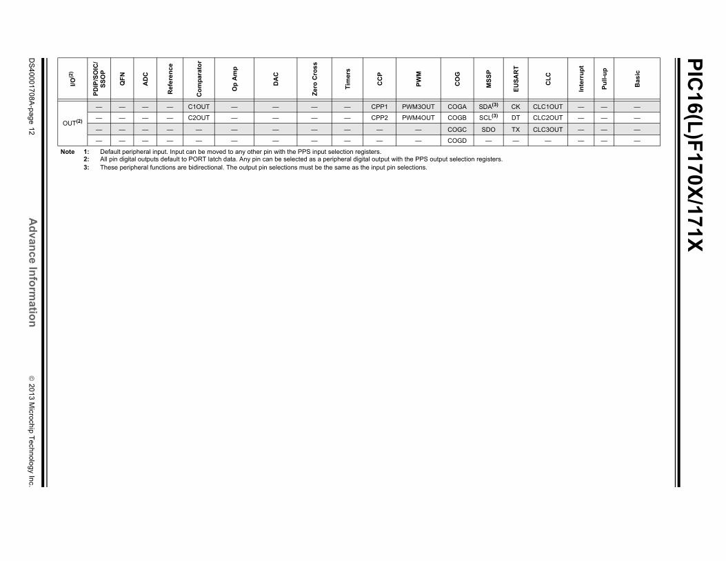
OUT(2)
— — — — C1OUT — — — — CPP1 PWM3OUT COGA SDA(3
— — — — C2OUT — — — — CPP2 PWM4OUT COGB SCL(3
— — — — — — — — — — — COGC SDO
— — — — — — — — — — — COGD —
I/O(2
)
PDIP
/SO
IC/
SSO
P
QFN
AD
C
Ref
eren
ce
Com
para
tor
Op
Am
p
DA
C
Zero
Cro
ss
Tim
ers
CC
P
PWM
CO
G
MSS
P
Note 1: Default peripheral input. Input can be moved to any other pin with the PPS input selection registers. 2: All pin digital outputs default to PORT latch data. Any pin can be selected as a peripheral digital output with the PPS output selection registe3: These peripheral functions are bidirectional. The output pin selections must be the same as the input pin selections.

2013 M
icrochip Technology Inc.A
dvance Information
DS
40001708A-page 13
PIC16(L)F170X/171X
TA
Inte
rrup
t
Pull-
up
Bas
ic
R CLCIN0(1) IOC Y
R CLCIN1(1) IOC Y
R IOC Y
R IOC YR IOC YR IOC Y
R IOCOSC2
CLKOUT
R IOCOSC1CLKIN
R INT(1)
IOC
R IOC
R IOC
R IOC
R IOC YR IOC Y
R CLCIN2(1) IOC Y ICSPCLK
R CLCIN3(1) IOC Y ICSPDAT
R IOC Y
R IOC Y
R IOC Y
No
No egisters.
No
No
No
EUSA
RT
CLC
R YIOC
BLE 5: 28-PIN ALLOCATION TABLE (PIC16L(F)1713/6/8) (PART 1)I/O
(2)
PDIP
,SO
IC,
SSO
P
QFN
, UQ
FN
AD
C
Ref
eren
ce
Op
Am
p
DA
C
Zero
Cro
ss
NC
O
A0 2 27 AN0
A1 3 28 AN1 OPA1OUT
A2 4 1 AN2 Vref- DAC1OUT1
A3 5 2 AN3 Vref+A4 6 3 OPA1IN+ T0CKI(1)
A5 7 4 AN4 OPA1IN- DAC2OUT1 nSS(1)
A6 10 7
A7 9 6 NCOCLK
B0 21 18 AN12 ZCD
B1 22 19 AN10 OPA2OUT
B2 23 20 AN8 OPA2IN-
B3 24 21 AN9 OPA2IN+
B4 25 22 AN11B5 26 23 AN13 T1G(1)
B6 27 24 SCL(1)
B7 28 25DAC1OUT2DAC2OUT2
T1CKI(1)
SOSCO
C1 12 9 SOSCI
C2 13 10 AN14
C3 14 11 AN15 SCK(1)
te 1: Default peripheral input. Alternate pins can be selected as the peripheral input with the PPS input selection registers.
te 2: All pin digital outputs default to PORT latch data. Alternate outputs can be selected as the peripheral digital output with the PPS output selection r
te 3: These peripheral functions are bidirectional. The output pin selections must be the same as the input pin selections.
te 4: Alternate outputs are excluded from solid shaded areas.
te 5: Alternate inputs are excluded from dot shaded areas.
C1IN1+
Com
para
tor
Tim
ers
CC
P
PWM
C1IN0-C2IN0-
C1IN1-C2IN1-
C1IN0+C2IN0+
CO
G
MSS
P
C2IN1+ COGIN(1)
C1IN3-C2IN3-
C1IN2-C2IN2-
C0 11 8
CCP2(1)
CCP1(1)

PIC16(L)F170X/171X
DS
40001708A-page 14
Advance Inform
ation
2013 Microchip Technology Inc.
Inte
rrup
t
Pull-
up
Bas
ic
DI(1) IOC Y
DA(1)
IOC YIOC YIOC Y
MCLRVppVddVss
SC
K/S
CL(3
)
SD
O
TX/C
K
DT(
3)
CLC
1OU
T
CLC
2OU
T
CLC
3OU
T
CLC
4OU
T
SC
K/S
CL(3
)
SS
RX
(3)
CK
CLC
IN0
CLC
IN1
CLC
IN2
CLC
IN3
INT
ction registers.
RX(3)CK(3)
CLC
MSS
P
EUSA
RT
TABLE 6: 28-PIN ALLOCATION TABLE (PIC16L(F)1713/6/8) (PART 2)I/O
(2)
PDIP
,SO
IC,
SSO
P
QFN
, UQ
FN
AD
C
Ref
eren
ce
Op
Am
p
DA
C
Zero
Cro
ss
NC
O
S
SRC5 16 13 AN17RC6 17 14 AN18RC7 18 15 AN19
RE3 1 26
Vdd 20 178 519 16
OUT(4)
C1O
UT
C2O
UT
CC
P1
CC
P2
NC
OO
UT
PW
M3O
UT
PW
M4O
UT
CO
GA
CO
GB
CO
GC
CO
GD
SD
A(3)
IN(5)
T1G
T1C
KI
T0C
KI
CC
P1
CC
P2
NC
OC
LK
SD
I
Note 1: Default peripheral input. Alternate pins can be selected as the peripheral input with the PPS input selection registers.
Note 2: All pin digital outputs default to PORT latch data. Alternate outputs can be selected as the peripheral digital output with the PPS output sele
Note 3: These peripheral functions are bidirectional. The output pin selections must be the same as the input pin selections.
Note 4: Alternate outputs are excluded from solid shaded areas.
Note 5: Alternate inputs are excluded from dot shaded areas.
RC4 15 12 AN16
Com
para
tor
Tim
ers
CO
GIN
Vss
CC
P
PWM
CO
G

2013 M
icrochip Technology Inc.A
dvance Information
DS
40001708A-page 15
PIC16(L)F170X/171X
TA
Inte
rrup
t
Pul
lup
Basi
c
CLCIN0(1) IOC Y
CLCIN1(1) IOC Y
IOC Y
IOC YIOC YIOC Y
IOC OSC2CLKOUT
IOC OSC1CLKIN
INT(1)
IOC
IOC
IOC
IOC
IOC YIOC Y
CLCIN2(1) IOC Y ICSPCLK
CLCIN3(1) IOC Y ICSPDAT
IOC Y
IOC YIOC YIOC Y
registers.
CLC
EUS
ART
YIOC
BLE 7: PIN ALLOCATION TABLE (PIC16L(F)1717/9) (PART 1)I/O
(2)
PDI
P
TQFP
UQFN
ADC
Ref
eren
ce
Op
Am
p
DAC
Zero
Cro
ss
NCO
RA0 2 19 17 AN0
RA1 3 20 18 AN1 OPA1OUT
RA2 4 21 19 AN2 Vref- DAC1OUT1
RA3 5 22 20 AN3 Vref+RA4 6 23 21 OPA1IN+ T0CKI(1)
RA5 7 24 22 AN4 OPA1IN- DAC2OUT1 nSS(1)
RA6 14 31 29
RA7 13 30 28 NCOCLK
RB0 33 8 8 AN12 ZCD
RB1 34 9 9 AN10 OPA2OUT
RB2 35 10 10 AN8 OPA2IN-
RB3 36 11 11 AN9 OPA2IN+
RB4 37 14 12 AN11RB5 38 15 13 AN13 T1G(1)
RB6 39 16 14 SCL(1)
RB7 40 17 15 DAC1OUT2DAC2OUT2
T1CKI(1)
SOSCO
RC1 16 35 31 SOSCI
RC2 17 36 32 AN14RC3 18 37 33 AN15 SCK(1)
SDI(1)
SDA(1)
Note 1: Default peripheral input. Alternate pins can be selected as the peripheral input with the PPS input selection registers. Note 2: All pin digital outputs default to PORT latch data. Alternate outputs can be selected as the peripheral digital output with the PPS output selection
Note 3: These peripheral functions are bidirectional. The output pin selections must be the same as the input pin selections.Note 4: Alternate outputs are excluded from solid shaded areas.
COG
COGIN(1)
PWM
Com
para
tor
C2IN1+
C1IN3-C2IN3-
C1IN2-C2IN2-
C1IN0-C2IN0-
C1IN1-C2IN1-
C1IN0+C2IN0+C1IN1+
CCP
CCP2(1)
CCP1(1)
MSS
P
Tim
ers
RC0 15 32 30
RC4 23 42 38 AN16
PIC16(L)F170X/171X
DS
40001708A-page 16
Advance Inform
ation
2013 Microchip Technology Inc.
Inte
rrup
t
Pullu
p
Basi
c
IOC YIOC YIOC Y
MCLRVppVdd
Vss
SC
K/S
CL(3
)
SD
O
TX/C
K
DT
(3)
CLC
1OU
T
CLC
2OU
T
CLC
3OU
T
CLC
4OU
T
SC
K/S
CL(3
)
SS
RX
(3)
CK
CLC
IN0
CLC
IN1
CLC
IN2
CLC
IN3
INT
ut selection registers.
EUSA
RT
CLC
RX(3)CK(3)
MSS
P
TABLE 8: PIN ALLOCATION TABLE (PIC16L(F)1717/9) (PART 2I/O
(2)
PDIP
TQFP
UQ
FN
ADC
Refe
renc
e
Op
Am
p
DAC
Zero
Cro
ss
NCO
RC5 24 43 39 AN17RC6 25 44 40 AN18RC7 26 1 1 AN19RD0 19 38 34 AN20RD1 20 39 35 AN21RD2 21 40 36 AN22RD3 22 41 37 AN23RD4 27 2 2 AN24RD5 28 3 3 AN25RD6 29 4 4 AN26RD7 30 5 5RE0 8 25 23 AN5RE1 9 26 24 AN6RE2 10 27 25 AN7
RE3 1 18 16
11 7 732 28 2612 6 631 29 27
OUT(4)
C1O
UT
C2O
UT
CC
P1
CC
P2
NC
OO
UT
PW
M3O
UT
PW
M4O
UT
CO
GA
CO
GB
CO
GC
CO
GD
SD
A(3
)
IN(5)
T1G
T1C
KI
T0C
KI
CC
P1
CC
P2
NC
OC
LK
SD
I
Note 1: Default peripheral input. Alternate pins can be selected as the peripheral input with the PPS input selection registers. Note 2: All pin digital outputs default to PORT latch data. Alternate outputs can be selected as the peripheral digital output with the PPS outp
Note 3: These peripheral functions are bidirectional. The output pin selections must be the same as the input pin selections.Note 4: Alternate outputs are excluded from solid shaded areas.Note 5: Alternate inputs are excluded from dot shaded areas.
Com
para
tor
Tim
ers
CCP
PWM
CO
G
Vdd
Vss
CO
GIN

Note the following details of the code protection feature on Microchip devices:• Microchip products meet the specification contained in their particular Microchip Data Sheet.
• Microchip believes that its family of products is one of the most secure families of its kind on the market today, when used in the intended manner and under normal conditions.
• There are dishonest and possibly illegal methods used to breach the code protection feature. All of these methods, to our knowledge, require using the Microchip products in a manner outside the operating specifications contained in Microchip’s Data Sheets. Most likely, the person doing so is engaged in theft of intellectual property.
• Microchip is willing to work with the customer who is concerned about the integrity of their code.
• Neither Microchip nor any other semiconductor manufacturer can guarantee the security of their code. Code protection does not mean that we are guaranteeing the product as “unbreakable.”
Code protection is constantly evolving. We at Microchip are committed to continuously improving the code protection features of ourproducts. Attempts to break Microchip’s code protection feature may be a violation of the Digital Millennium Copyright Act. If such actsallow unauthorized access to your software or other copyrighted work, you may have a right to sue for relief under that Act.
Information contained in this publication regarding deviceapplications and the like is provided only for your convenienceand may be superseded by updates. It is your responsibility toensure that your application meets with your specifications.MICROCHIP MAKES NO REPRESENTATIONS ORWARRANTIES OF ANY KIND WHETHER EXPRESS ORIMPLIED, WRITTEN OR ORAL, STATUTORY OROTHERWISE, RELATED TO THE INFORMATION,INCLUDING BUT NOT LIMITED TO ITS CONDITION,QUALITY, PERFORMANCE, MERCHANTABILITY ORFITNESS FOR PURPOSE. Microchip disclaims all liabilityarising from this information and its use. Use of Microchipdevices in life support and/or safety applications is entirely atthe buyer’s risk, and the buyer agrees to defend, indemnify andhold harmless Microchip from any and all damages, claims,suits, or expenses resulting from such use. No licenses areconveyed, implicitly or otherwise, under any Microchipintellectual property rights.
2013 Microchip Technology Inc. Advance Info
QUALITY MANAGEMENT SYSTEM CERTIFIED BY DNV
== ISO/TS 16949 ==
Trademarks
The Microchip name and logo, the Microchip logo, dsPIC, FlashFlex, KEELOQ, KEELOQ logo, MPLAB, PIC, PICmicro, PICSTART, PIC32 logo, rfPIC, SST, SST Logo, SuperFlash and UNI/O are registered trademarks of Microchip Technology Incorporated in the U.S.A. and other countries.
FilterLab, Hampshire, HI-TECH C, Linear Active Thermistor, MTP, SEEVAL and The Embedded Control Solutions Company are registered trademarks of Microchip Technology Incorporated in the U.S.A.
Silicon Storage Technology is a registered trademark of Microchip Technology Inc. in other countries.
Analog-for-the-Digital Age, Application Maestro, BodyCom, chipKIT, chipKIT logo, CodeGuard, dsPICDEM, dsPICDEM.net, dsPICworks, dsSPEAK, ECAN, ECONOMONITOR, FanSense, HI-TIDE, In-Circuit Serial Programming, ICSP, Mindi, MiWi, MPASM, MPF, MPLAB Certified logo, MPLIB, MPLINK, mTouch, Omniscient Code Generation, PICC, PICC-18, PICDEM, PICDEM.net, PICkit, PICtail, REAL ICE, rfLAB, Select Mode, SQI, Serial Quad I/O, Total Endurance, TSHARC, UniWinDriver, WiperLock, ZENA and Z-Scale are trademarks of Microchip Technology Incorporated in the U.S.A. and other countries.
SQTP is a service mark of Microchip Technology Incorporated in the U.S.A.
GestIC and ULPP are registered trademarks of Microchip Technology Germany II GmbH & Co. KG, a subsidiary of Microchip Technology Inc., in other countries.
All other trademarks mentioned herein are property of their respective companies.
© 2013, Microchip Technology Incorporated, Printed in the U.S.A., All Rights Reserved.
Printed on recycled paper.
ISBN: 9781620772942
Microchip received ISO/TS-16949:2009 certification for its worldwide
rmation DS40001708A-page 17
headquarters, design and wafer fabrication facilities in Chandler and Tempe, Arizona; Gresham, Oregon and design centers in California and India. The Company’s quality system processes and procedures are for its PIC® MCUs and dsPIC® DSCs, KEELOQ® code hopping devices, Serial EEPROMs, microperipherals, nonvolatile memory and analog products. In addition, Microchip’s quality system for the design and manufacture of development systems is ISO 9001:2000 certified.
DS40001708A-page 18 Advance Information 2013 Microchip Technology Inc.
AMERICASCorporate Office2355 West Chandler Blvd.Chandler, AZ 85224-6199Tel: 480-792-7200 Fax: 480-792-7277Technical Support: http://www.microchip.com/supportWeb Address: www.microchip.comAtlantaDuluth, GA Tel: 678-957-9614 Fax: 678-957-1455BostonWestborough, MA Tel: 774-760-0087 Fax: 774-760-0088ChicagoItasca, IL Tel: 630-285-0071 Fax: 630-285-0075ClevelandIndependence, OH Tel: 216-447-0464 Fax: 216-447-0643DallasAddison, TX Tel: 972-818-7423 Fax: 972-818-2924DetroitFarmington Hills, MI Tel: 248-538-2250Fax: 248-538-2260IndianapolisNoblesville, IN Tel: 317-773-8323Fax: 317-773-5453Los AngelesMission Viejo, CA Tel: 949-462-9523 Fax: 949-462-9608Santa ClaraSanta Clara, CA Tel: 408-961-6444Fax: 408-961-6445TorontoMississauga, Ontario, CanadaTel: 905-673-0699 Fax: 905-673-6509
ASIA/PACIFICAsia Pacific OfficeSuites 3707-14, 37th FloorTower 6, The GatewayHarbour City, KowloonHong KongTel: 852-2401-1200Fax: 852-2401-3431Australia - SydneyTel: 61-2-9868-6733Fax: 61-2-9868-6755China - BeijingTel: 86-10-8569-7000 Fax: 86-10-8528-2104China - ChengduTel: 86-28-8665-5511Fax: 86-28-8665-7889China - ChongqingTel: 86-23-8980-9588Fax: 86-23-8980-9500China - HangzhouTel: 86-571-2819-3187 Fax: 86-571-2819-3189China - Hong Kong SARTel: 852-2943-5100 Fax: 852-2401-3431China - NanjingTel: 86-25-8473-2460Fax: 86-25-8473-2470China - QingdaoTel: 86-532-8502-7355Fax: 86-532-8502-7205China - ShanghaiTel: 86-21-5407-5533 Fax: 86-21-5407-5066China - ShenyangTel: 86-24-2334-2829Fax: 86-24-2334-2393China - ShenzhenTel: 86-755-8864-2200 Fax: 86-755-8203-1760China - WuhanTel: 86-27-5980-5300Fax: 86-27-5980-5118China - XianTel: 86-29-8833-7252Fax: 86-29-8833-7256China - XiamenTel: 86-592-2388138 Fax: 86-592-2388130China - ZhuhaiTel: 86-756-3210040 Fax: 86-756-3210049
ASIA/PACIFICIndia - BangaloreTel: 91-80-3090-4444 Fax: 91-80-3090-4123India - New DelhiTel: 91-11-4160-8631Fax: 91-11-4160-8632India - PuneTel: 91-20-2566-1512Fax: 91-20-2566-1513Japan - OsakaTel: 81-6-6152-7160 Fax: 81-6-6152-9310Japan - TokyoTel: 81-3-6880- 3770 Fax: 81-3-6880-3771Korea - DaeguTel: 82-53-744-4301Fax: 82-53-744-4302Korea - SeoulTel: 82-2-554-7200Fax: 82-2-558-5932 or 82-2-558-5934Malaysia - Kuala LumpurTel: 60-3-6201-9857Fax: 60-3-6201-9859Malaysia - PenangTel: 60-4-227-8870Fax: 60-4-227-4068Philippines - ManilaTel: 63-2-634-9065Fax: 63-2-634-9069SingaporeTel: 65-6334-8870Fax: 65-6334-8850Taiwan - Hsin ChuTel: 886-3-5778-366Fax: 886-3-5770-955Taiwan - KaohsiungTel: 886-7-213-7828Fax: 886-7-330-9305Taiwan - TaipeiTel: 886-2-2508-8600 Fax: 886-2-2508-0102Thailand - BangkokTel: 66-2-694-1351Fax: 66-2-694-1350
EUROPEAustria - WelsTel: 43-7242-2244-39Fax: 43-7242-2244-393Denmark - CopenhagenTel: 45-4450-2828 Fax: 45-4485-2829France - ParisTel: 33-1-69-53-63-20 Fax: 33-1-69-30-90-79Germany - MunichTel: 49-89-627-144-0 Fax: 49-89-627-144-44Italy - Milan Tel: 39-0331-742611 Fax: 39-0331-466781Netherlands - DrunenTel: 31-416-690399 Fax: 31-416-690340Spain - MadridTel: 34-91-708-08-90Fax: 34-91-708-08-91UK - WokinghamTel: 44-118-921-5869Fax: 44-118-921-5820
Worldwide Sales and Service
11/29/12