pic24h family overview
TRANSCRIPT

© 2005 Microchip Technology Inc. Preliminary DS70166A
PIC24HFamily Overview
High-Performance 16-BitMicrocontrollers

Note the following details of the code protection feature on Microchip devices:• Microchip products meet the specification contained in their particular Microchip Data Sheet.
• Microchip believes that its family of products is one of the most secure families of its kind on the market today, when used in the intended manner and under normal conditions.
• There are dishonest and possibly illegal methods used to breach the code protection feature. All of these methods, to our knowledge, require using the Microchip products in a manner outside the operating specifications contained in Microchip’s Data Sheets. Most likely, the person doing so is engaged in theft of intellectual property.
• Microchip is willing to work with the customer who is concerned about the integrity of their code.
• Neither Microchip nor any other semiconductor manufacturer can guarantee the security of their code. Code protection does not mean that we are guaranteeing the product as “unbreakable.”
Code protection is constantly evolving. We at Microchip are committed to continuously improving the code protection features of ourproducts. Attempts to break Microchip’s code protection feature may be a violation of the Digital Millennium Copyright Act. If such actsallow unauthorized access to your software or other copyrighted work, you may have a right to sue for relief under that Act.
Information contained in this publication regarding deviceapplications and the like is provided only for your convenienceand may be superseded by updates. It is your responsibility toensure that your application meets with your specifications.MICROCHIP MAKES NO REPRESENTATIONS OR WAR-RANTIES OF ANY KIND WHETHER EXPRESS OR IMPLIED,WRITTEN OR ORAL, STATUTORY OR OTHERWISE,RELATED TO THE INFORMATION, INCLUDING BUT NOTLIMITED TO ITS CONDITION, QUALITY, PERFORMANCE,MERCHANTABILITY OR FITNESS FOR PURPOSE.Microchip disclaims all liability arising from this information andits use. Use of Microchip’s products as critical components inlife support systems is not authorized except with expresswritten approval by Microchip. No licenses are conveyed,implicitly or otherwise, under any Microchip intellectual propertyrights.
DS70166A-page ii Prelimin
Trademarks
The Microchip name and logo, the Microchip logo, Accuron, dsPIC, KEELOQ, microID, MPLAB, PIC, PICmicro, PICSTART, PRO MATE, PowerSmart, rfPIC, and SmartShunt are registered trademarks of Microchip Technology Incorporated in the U.S.A. and other countries.
AmpLab, FilterLab, Migratable Memory, MXDEV, MXLAB, PICMASTER, SEEVAL, SmartSensor and The Embedded Control Solutions Company are registered trademarks of Microchip Technology Incorporated in the U.S.A.
Analog-for-the-Digital Age, Application Maestro, dsPICDEM, dsPICDEM.net, dsPICworks, ECAN, ECONOMONITOR, FanSense, FlexROM, fuzzyLAB, In-Circuit Serial Programming, ICSP, ICEPIC, Linear Active Thermistor, MPASM, MPLIB, MPLINK, MPSIM, PICkit, PICDEM, PICDEM.net, PICLAB, PICtail, PowerCal, PowerInfo, PowerMate, PowerTool, rfLAB, rfPICDEM, Select Mode, Smart Serial, SmartTel, Total Endurance and WiperLock are trademarks of Microchip Technology Incorporated in the U.S.A. and other countries.
SQTP is a service mark of Microchip Technology Incorporated in the U.S.A.
All other trademarks mentioned herein are property of their respective companies.
© 2005, Microchip Technology Incorporated, Printed in the U.S.A., All Rights Reserved.
Printed on recycled paper.
ary © 2005 Microchip Technology Inc.
Microchip received ISO/TS-16949:2002 quality system certification for its worldwide headquarters, design and wafer fabrication facilities in Chandler and Tempe, Arizona and Mountain View, California in October 2003. The Company’s quality system processes and procedures are for its PICmicro® 8-bit MCUs, KEELOQ® code hopping devices, Serial EEPROMs, microperipherals, nonvolatile memory and analog products. In addition, Microchip’s quality system for the design and manufacture of development systems is ISO 9001:2000 certified.

PIC24HPIC24H High-Performance 16-Bit MCU Overview
Operating Range• DC – 40 MIPS (40 MIPS @ 3.0-3.6V, -40° to +85°C)• Industrial temperature range (-40° to +85°C)
High-Performance DSC CPU• Modified Harvard architecture• C compiler optimized instruction set• 16-bit wide data path• 24-bit wide instructions• Linear program memory addressing up to 4M
instruction words• Linear data memory addressing up to 64 Kbytes• 74 base instructions: mostly 1 word/1 cycle• Sixteen 16-bit general-purpose registers• Flexible and powerful addressing modes• Software stack• 16 x 16 integer multiply operations• 32/16 and 16/16 divide operations• Single-cycle multiply• Up to ± 16-bit shifts
Direct Memory Access (DMA)• 8-channel hardware DMA• Allows data transfer between RAM and a
peripheral while CPU is executing code (no cycle stealing)
• 2 KB of dual-ported DMA buffer area (DMA RAM) to store data transferred via DMA
• Most peripherals support DMA
Interrupt Controller• 5-cycle latency• 118 interrupt vectors• Up to 61 available interrupt sources, up to
5 external interrupts• 7 programmable priority levels• 5 processor exceptions
Digital I/O• Up to 85 programmable digital I/O pins• Wake-up/Interrupt-on-Change on up to 24 pins• Output pins can drive from 3.0V to 3.6V• All digital input pins are 5V tolerant• 4 mA sink and source on all I/O pins
On-Chip Flash and SRAM• Flash program memory, up to 256 Kbytes• Data SRAM (up to 30 Kbytes):
- Includes 2 KB of DMA RAM
System Management• Flexible clock options:
- External, crystal, resonator, internal RC- Fully integrated PLL- Extremely low jitter PLL
• Power-up timer• Oscillator Start-up Timer/Stabilizer• Watchdog timer with its own RC oscillator• Fail-Safe Clock Monitor• Reset by multiple sources
Power Management• On-chip 2.5V voltage regulator• Switch between clock sources in real time• Idle, Sleep and Doze modes with fast wake-up
© 2005 Microchip Technology Inc. Preliminary DS70166A-page 1

PIC24H
Timers/Capture/Compare/PWM• Timer/Counters: up to nine 16-bit timers:- Can pair up to make four 32-bit timers- 1 timer runs as Real-Time Clock with external
32 kHz oscillator- Programmable prescaler
• Input Capture (up to 8 channels):- Capture on up, down or both edges- 16-bit capture input functions- 4-deep FIFO on each capture
• Output Compare (up to 8 channels):- Single or Dual 16-Bit Compare mode- 16-Bit Glitchless PWM mode
Communication Modules• 3-wire SPI™ (up to 2 modules):
- Framing supports I/O interface to simple codecs
- Supports 8-bit and 16-bit data- Supports all serial clock formats and
sampling modes- 8-word FIFO buffers
• I2C™ (up to 2 modules):- Full Multi-Master Slave mode support- 7-bit and 10-bit addressing- Bus collision detection and arbitration- Integrated signal conditioning- Address masking
• UART (up to 2 modules):- Interrupt-on-address bit detect- Wake-up-on-Start bit from Sleep mode- 4-character TX and RX FIFO buffers- LIN bus support- IrDA® encoding and decoding in hardware- High-Speed Baud mode
• Enhanced CAN 2.0B active (up to 2 modules):- Up to 8 transmit and up to 32 receive buffers - 16 receive filters and 3 masks- Loopback, Listen Only and Listen All
Messages modes for diagnostics and bus monitoring
- Wake-up on CAN message- FIFO mode using DMA
Analog-to-Digital Converters (ADC)• Up to two 10-bit or 12-bit ADC modules in a
device• 10-bit 2.2 Msps or 12-bit 1 Msps conversion:
- 2, 4 or 8 simultaneous samples- Up to 32 input channels with auto-scanning- Conversion start can be manual or
synchronized with 1 of 4 trigger sources- Conversion possible in Sleep mode- ±1 LSB max integral nonlinearity- ±1 LSB max differential nonlinearity
CMOS Flash Technology• Low-power, high-speed Flash technology• Fully static design• 3.3V (+/- 10%) operating voltage• Industrial temperature• Low-power consumption
Packaging:• 100-pin TQFP (14x14x1 mm and 12x12x1 mm)• 64-pin TQFP (10x10x1 mm)
Note: See Table 1-1 for exact peripheral features per device.
DS70166A-page 2 Preliminary © 2005 Microchip Technology Inc.

PIC24H
1.0 PIC24H PRODUCT FAMILIES
1.1 General-Purpose FamilyThe PIC24H General-purpose Family (Table 1-1)is ideal for a wide variety of 16-bit MCU embeddedapplications. The variants with codec interfaces arewell-suited for audio applications.
TABLE 1-1: PIC24H GENERAL-PURPOSE FAMILY VARIANTS
Device Pins Program Flash Memory (KB) R
AM
(1)
(KB
)
DM
A C
hann
els
Tim
er 1
6-bi
t
Inpu
t Cap
ture
Out
put C
ompa
reSt
d. P
WM
Cod
ecIn
terf
ace
AD
C
UA
RT
SPI™
I2 C™
CA
N
I/O P
ins
(Max
)(2)
Packages
24HJ64GP206 64 64 8 8 9 8 8 0 1 ADC, 18 ch
2 2 1 0 53 PT
24HJ64GP210 100 64 8 8 9 8 8 0 1 ADC, 32 ch
2 2 2 0 85 PT
24HJ64GP506 64 64 8 8 9 8 8 0 1 ADC, 18 ch
2 2 2 1 53 PF, PT
24HJ64GP510 100 64 8 8 9 8 8 0 1 ADC, 32 ch
2 2 2 1 85 PT
24HJ128GP206 64 128 8 8 9 8 8 0 1 ADC, 18 ch
2 2 2 0 53 PT
24HJ128GP210 100 128 8 8 9 8 8 0 1 ADC, 32 ch
2 2 2 0 85 PF, PT
24HJ128GP506 64 128 8 8 9 8 8 0 1 ADC, 18 ch
2 2 2 1 53 PT
24HJ128GP510 100 128 8 8 9 8 8 0 1 ADC, 32 ch
2 2 2 1 85 PT
24HJ128GP306 64 128 16 8 9 8 8 0 1 ADC, 18 ch
2 2 2 0 53 PF, PT
24HJ128GP310 100 128 16 8 9 8 8 0 1 ADC, 32 ch
2 2 2 0 85 PT
24HJ256GP206 64 256 16 8 9 8 8 0 1 ADC, 18 ch
2 2 2 0 53 PT
24HJ256GP210 100 256 16 8 9 8 8 0 1 ADC, 32 ch
2 2 2 0 85 PF, PT
24HJ256GP610 100 256 16 8 9 8 8 0 2 ADC, 32 ch
2 2 2 2 85 PF, PT
Note 1: RAM size is inclusive of 2 KB DMA RAM.2: Maximum I/O pin count includes pins shared by the peripheral functions.
© 2005 Microchip Technology Inc. Preliminary DS70166A-page 3

PIC24H
PRODUCT IDENTIFICATION SYSTEM
Architecture 24 = 16-bit Microcontroller
Flash Memory Family HJ = Flash program memory, 3.3V, high-speed
Program Memory Size 64 = 64 Kbytes128 = 128 Kbytes256 = 256 Kbytes
Product Group GP2 = General Purpose familyGP3 = General Purpose familyGP5 = General Purpose familyGP6 = General Purpose family
Tape & Reel T = ApplicableBlank = Not applicable
Pin Count 06 = 64-pin10 = 100-pin
Temperature Range I = -40°C to +85°C (Industrial)
Package PT = 10x10 or 12x12 mm TQFP (Thin Quad Flatpack)PF = 14x14 mm TQFP (Thin Quad Flatpack)
Pattern Three-digit QTP, SQTP, Code or Special Requirements (blank otherwise)ES = Engineering Sample
Examples:a) dsPIC24HJ64GP610I/PT:
General Purpose dsPIC24H, 64 KB program memory, 100-pin, Industrial temp.,TQFP package.
b) dsPIC24HJ64GP206I/PT-ES:Motor Control dsPIC24H, 64 KB program memory, 64-pin, Industrial temp.,TQFP package, Engineering Sample.
Microchip TrademarkArchitectureFlash Memory FamilyProgram Memory Size (KB)Product GroupPin Count
Temperature RangePackagePattern
PIC 24 HJ 256 GP6 10 T I / PT - XXX
Tape and Reel Flag (if applicable)
DS70166A-page 4 Preliminary © 2005 Microchip Technology Inc.

PIC24H
2.0 PIC24H DEVICE FAMILY OVERVIEW
The PIC24H device family employs a powerful 16-bitmicrocontroller (MCU). The resulting CPU functionalityis ideal for applications that rely on high-speed,repetitive computations, as well as control.
Flexible and deterministic interrupt handling, coupledwith a powerful array of peripherals, renders thePIC24H devices suitable for control applications.
Further, Direct Memory Access (DMA) enablesoverhead-free transfer of data between severalperipherals and a dedicated DMA RAM. Reliable, fieldprogrammable Flash program memory ensuresscalability of applications that use PIC24H devices.
Figure 2-1 shows a sample device block diagramtypical of the PIC24H product family.
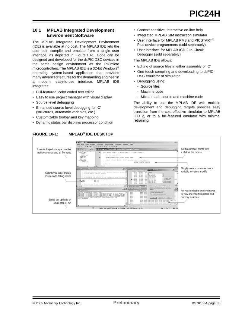
FIGURE 2-1: PIC24H DEVICE BLOCK DIAGRAM
Shifter
Divide Control
17 x 17 Multiplier
W RegisterArray
16 x 16MemoryMapped
16-bit ALU
Program Flash Memory Data
Access
AGU
Program Counter<23 bits>
InstructionPrefetch & Decode
X-Data Bus <16-bit>
Data SRAM up to
28 Kbytes
FlashProgramMemory
up to256 Kbytes
Peripherals
I/O Ports
24
23
Legend:MCU/DSP X-Data PathAddress Path
STATUS Register Dual PortRAM
2 KbytesDMA
Controller
© 2005 Microchip Technology Inc. Preliminary DS70166A-page 5

PIC24H
3.0 CPU ARCHITECTURE
3.1 OverviewThe PIC24H CPU module has a 16-bit (data) modifiedHarvard architecture with an enhanced instruction set.The CPU has a 24-bit instruction word with a variablelength opcode field. The Program Counter (PC) is23 bits wide and addresses up to 4M x 24 bits of userprogram memory space. The actual amount of programmemory implemented, as illustrated in Figure 3-1,varies from one device to another. A single-cycleinstruction prefetch mechanism is used to helpmaintain throughput and provides predictableexecution. All instructions execute in a single cycle,with the exception of instructions that change theprogram flow, the double word move (MOV.D)instruction and the table instructions. Overhead-freeprogram loop constructs are supported using theREPEAT instruction, which is interruptible at any point.
The PIC24H devices have sixteen 16-bit workingregisters in the programmer’s model. Each of theworking registers can serve as a data, address oraddress offset register. The 16th working register(W15) operates as a software Stack Pointer (SP) forinterrupts and calls.
The PIC24H instruction set includes many addressingmodes and is designed for optimum C compilerefficiency.
3.1.1 DATA MEMORY OVERVIEWThe data space can be addressed as 32K words or64 Kbytes. Reads and writes are performed using anAddress Generation Unit (AGU), which accesses theentire memory map as one linear data space.
The upper 32 Kbytes of the data space memory mapcan optionally be mapped into program space at any16K program word boundary defined by the 8-bitProgram Space Visibility Page (PSVPAG) register. Theprogram-to-data space mapping feature lets anyinstruction access program space as if it were dataspace.
The data space includes 2 Kbytes of DMA RAM, whichis primarily used for DMA data transfers, but may beused as general-purpose RAM.
FIGURE 3-1: PROGRAM SPACE MEMORY MAP
Reset – Target Address
Use
r Mem
ory
Spa
ce
000000
0000FE
Reserved 000002
000100
Device Configuration
User FlashProgram Memory
02AC0002ABFE
Con
figur
atio
n M
emor
yS
pace
Osc. Fail Trap VectorAddress Error Trap Vector
Stack Error Trap VectorMath Error Trap Vector
DMA Error VectorReserved Vector
Interrupt Vector Table
(87552 x 24-bit)
800000
F80000Registers (12 x 8-bit) F80016
F80018
FFFFFE
F7FFFE
Reserved
000014 Vect
or
Reset – GOTO Instruction
000004
Reserved
7FFFFE
Reserved
0002000001FE
000104Alternate Vector Table
Reserved
Tabl
esReserved Vector
Device ID (2 x 16-bit)
Reserved
FEFFFEFF0000FF0002FF0004
DS70166A-page 6 Preliminary © 2005 Microchip Technology Inc.

PIC24H
3.1.2 ADDRESSING MODES OVERVIEWThe CPU supports Inherent (no operand), Relative,Literal, Memory Direct, Register Direct and RegisterIndirect Addressing modes. Each instruction isassociated with a predefined addressing mode groupdepending upon its functional requirements. As manyas 6 addressing modes are supported for eachinstruction.For most instructions, the PIC24H is capable ofexecuting a data (or program data) memory read, aworking register (data) read, a data memory write anda program (instruction) memory read per instructioncycle. As a result, three parameter instructions can besupported, allowing A + B = C operations to beexecuted in a single cycle.
3.1.3 SPECIAL MCU FEATURESThe PIC24H features a 17-bit by 17-bit, single-cyclemultiplier. The multiplier can perform signed, unsignedand mixed-sign multiplication. Using a 17-bit by 17-bitmultiplier for 16-bit by 16-bit multiplication allows you toperform mixed-sign multiplication.
The PIC24H supports 16/16 and 32/16 divideoperations, both fractional and integer. All divideinstructions are iterative operations. They must beexecuted within a REPEAT loop, resulting in a totalexecution time of 19 instruction cycles. The divideoperation can be interrupted during any of those 19cycles without loss of data.
A 40-bit data shifter is used to perform up to a 16-bit leftor right shift in a single cycle.
3.1.4 INTERRUPT OVERVIEWThe PIC24H has a vectored exception scheme with upto 5 sources of non-maskable traps and 67 interruptsources. Each interrupt source can be assigned to oneof seven priority levels.
3.1.5 FEATURES TO ENHANCE COMPILER EFFICIENCY
The CPU architecture possesses several features thatlead to a more efficient (code size and speed) Ccompiler.
1. For most instructions, three-parameter instruc-tions can be supported, allowing A + B = Coperations to be executed in a single cycle.
2. Instruction addressing modes are extremelyflexible to meet compiler needs.
3. The working register array consists of 16 x 16-bitregisters, each of which can act as data,address or offset registers. One working register(W15) operates as the software Stack Pointerfor interrupts and calls.
4. Linear indirect access of all data space ispossible, plus the memory direct address rangeis up to 8 Kbytes. This capability, together withthe addition of 16-bit direct address MOV-basedinstructions, has provided a contiguous linearaddressing space.
5. Linear indirect access of 32K word (64 Kbyte)pages within program space is possible, usingany working register via new table read andwrite instructions.
6. Part of data space can be mapped into programspace, allowing constant data to be accessed asif it were in data space.
© 2005 Microchip Technology Inc. Preliminary DS70166A-page 7

PIC24H
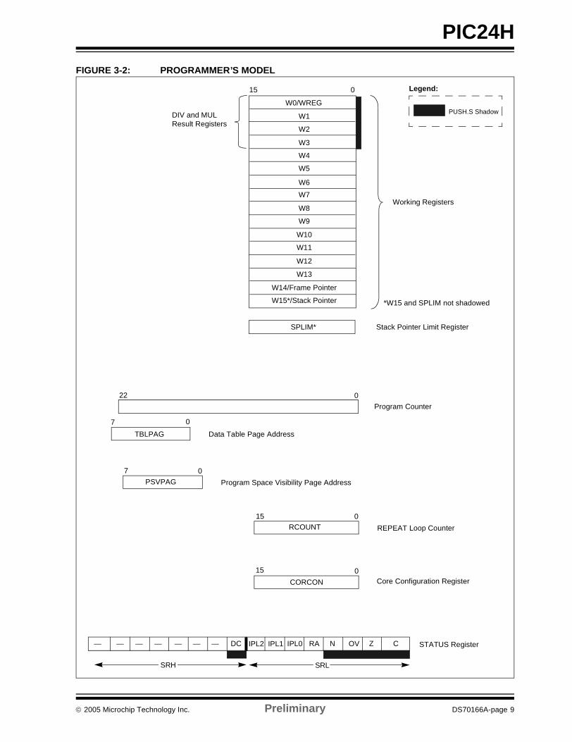
3.2 Programmer’s ModelThe programmer’s model, shown in Figure 3-2,consists of 16 x 16-bit working registers (W0 throughW15), STATUS register (SR), Data Table Page register(TBLPAG), Program Space Visibility Page register(PSVPAG), REPEAT count register (RCOUNT) andProgram Counter (PC). The working registers can actas data, address or offset registers. All registers arememory mapped. W0 is the W register for allinstructions that perform file register addressing.Some of these registers have a shadow registerassociated with them (see the legend in Figure 3-2).The shadow register is used as a temporary holdingregister and can transfer its contents to or from its hostregister upon some event occurring in a single cycle.None of the shadow registers are accessible directly.
When a byte operation is performed on a workingregister, only the Least Significant Byte (LSB) of thetarget register is affected. However, a benefit ofmemory mapped working registers is that both theLeast and Most Significant Bytes (MSBs) can bemanipulated through byte-wide data memory spaceaccesses.
W15 is the dedicated software Stack Pointer (SP). It isautomatically modified by exception processing andsubroutine calls and returns. However, W15 can bereferenced by any instruction in the same manner as allother W registers. This simplifies the reading, writingand manipulation of the Stack Pointer (e.g., creatingstack frames).
W14 has been dedicated as a Stack Frame Pointer, asdefined by the LNK and ULNK instructions. However,W14 can be referenced by any instruction in the samemanner as all other W registers.
The Stack Pointer always points to the first availablefree word and grows from lower addresses towardshigher addresses. It pre-decrements for stack pops(reads) and post-increments for stack pushes (writes).
DS70166A-page 8 Preliminary © 2005 Microchip Technology Inc.
PIC24H
FIGURE 3-2: PROGRAMMER’S MODELTABPAG
22 0
7 0
015
Program Counter
Data Table Page Address
STATUS Register
Working Registers
W1
W2
W3
W4
W5
W6W7
W8
W9
W10
W11
W12
W13
W14/Frame Pointer
W15*/Stack Pointer
PSVPAG7 0
Program Space Visibility Page Address
Z — — — —
RCOUNT15 0
REPEAT Loop Counter
IPL2 IPL1
SPLIM* Stack Pointer Limit Register
SRL
PUSH.S Shadow
— —
15 0 Core Configuration Register
Legend:
CORCON
— DC RA N
TBLPAG
PSVPAG
IPL0 OV
W0/WREG
SRH
C
DIV and MULResult Registers
*W15 and SPLIM not shadowed
© 2005 Microchip Technology Inc. Preliminary DS70166A-page 9

PIC24H
3.3 Data Address SpaceThe data space is accessed as one unified linearaddress range (for MCU instructions). The data spaceis accessed using the Address Generation Unit (AGU).All Effective Addresses (EAs) are 16 bits wide and pointto bytes within the data space. Therefore, the dataspace address range is 64 Kbytes or 32K words,though the implemented memory locations vary fromone device to another.3.3.1 DMA RAMEvery PIC24H device contains 2 Kbytes of DMA RAMlocated at the end of Y data space. Memory locations inthe DMA RAM space are accessible simultaneously bythe CPU and the DMA Controller module. DMA RAM isutilized by the DMA Controller to store data to betransferred to various peripherals using DMA, as well asdata transferred from various peripherals using DMA.
When the CPU and the DMA Controller attempt toconcurrently write to the same DMA RAM location, thehardware ensures that the CPU is given precedence inaccessing the DMA RAM location. Therefore, the DMARAM provides a reliable means of transferring DMAdata without ever having to stall the CPU.
3.3.2 DATA SPACE WIDTHThe core data width is 16 bits. All internal registers areorganized as 16-bit wide words. Data space memory isorganized in byte addressable, 16-bit wide blocks.Figure 3-3 depicts a sample data space memory mapfor the PIC24H device with 16 Kbytes of RAM.
3.3.3 DATA ALIGNMENTTo help maintain backward compatibility withPICmicro® MCU devices and improve data spacememory usage efficiency, the PIC24H instruction setsupports both word and byte operations. Data isaligned in data memory and registers as words, but alldata space EAs resolve to bytes. Data byte reads willread the complete word which contains the byte, usingthe Least Significant bit (LSb) of any EA to determinewhich byte to select.
As a consequence of this byte accessibility, all EffectiveAddress calculations are internally scaled. Forexample, the core would recognize that Post-ModifiedRegister Indirect Addressing mode, [Ws++], will resultin a value of Ws + 1 for byte operations and Ws + 2 forword operations.
All word accesses must be aligned to an even address.Misaligned word data fetches are not supported.Should a misaligned read or write be attempted, a trapwill then be executed, allowing the system and/or userto examine the machine state prior to execution of theaddress Fault.
DS70166A-page 10 Preliminary © 2005 Microchip Technology Inc.

PIC24H
FIGURE 3-3: SAMPLE DATA SPACE MEMORY MAP0x0000
0x07FE
SFR Space
0xFFFE
Data RAM
Least Significant ByteAddress16 Bits
LSBMSB
Most Significant ByteAddress
0x0001
0x07FF
0xFFFF
0x4000
OptionallyMappedinto ProgramMemory
Unimplemented
0x0801 0x0800
2-KbyteSFR Space
DMA RAM
0x3FFE
8-KbyteData Space
0x3FFF0x4001
0x47FF 0x47FE
Note: This data memory map is for the largest memory PIC24H device. Data memory maps for other devicesmay vary.
0x4801 0x4800
0x1FFF 0x1FFE
0x8001 0x8000
© 2005 Microchip Technology Inc. Preliminary DS70166A-page 11

PIC24H
4.0 DIRECT MEMORY ACCESSDirect Memory Access (DMA) is a very efficientmechanism of copying data between peripheral SFRs(e.g., UART Receive register, Input Capture 1 buffer)and buffers or variables stored in RAM with minimalCPU intervention. The DMA Controller canautomatically copy entire blocks of data, without theuser software having to read or write peripheral SpecialFunction Registers (SFRs) every time a peripheralinterrupt occurs. To exploit the DMA capability, thecorresponding user buffers or variables must belocated in DMA RAM space.
The DMA Controller features eight identical datatransfer channels, each with its own set of control andstatus registers. The UART, SPI, DCI, Input Capture,Output Compare, ECAN™ technology and ADCmodules can utilize DMA. Each DMA channel can beconfigured to copy data either from buffers stored inDMA RAM to peripheral SFRs or from peripheral SFRsto buffers in DMA RAM.
Each channel supports the following features:
• Word or byte-sized data transfers• Transfers from peripheral to DMA RAM or DMA
RAM to peripheral
• Indirect addressing of DMA RAM locations with or without automatic post-increment
• Peripheral Indirect Addressing – In some peripherals, the DMA RAM read/write addresses may be partially derived from the peripheral
• One-Shot Block Transfers – Terminating DMA transfer after one block transfer
• Continuous Block Transfers – Reloading DMA RAM buffer start address after every block transfer is complete
• Ping-Pong Mode – Switching between two DMA RAM start addresses between successive block transfers, thereby filling two buffers alternately
• Automatic or manual initiation of block transfers• Each channel can select from 32 possible
sources of data sources or destinations
For each DMA channel, a DMA interrupt request isgenerated when a block transfer is complete.Alternatively, an interrupt can be generated when half ofthe block has been filled. Additionally, a DMA error trapis generated in either of the following Fault conditions:
• DMA RAM data write collision between the CPU and a peripheral
• Peripheral SFR data write collision between the CPU and the DMA Controller
FIGURE 4-1: TOP LEVEL SYSTEM ARCHITECTURE USING A DEDICATED TRANSACTION BUS
CPU
SRAM DMA RAM
CPU Peripheral DS Bus
Peripheral 3
DMA
Peripheral
Non-DMA
SRAM X-Bus
PORT 2PORT 1
Peripheral 1
DMAReady
Peripheral 2
DMAReadyReady
Ready
DMA DS Bus
CPU DMA
CPU DMA CPU DMA
Peripheral Indirect Address
Note: CPU and DMA address buses are not shown for clarity.
DM
AC
ontro
l
DMA Controller
ChannelsDMA
DS70166A-page 12 Preliminary © 2005 Microchip Technology Inc.

PIC24H
5.0 EXCEPTION PROCESSINGThe PIC24H has four processor exceptions (traps) andup to 61 sources of interrupts, which must be arbitratedbased on a priority scheme.
The processor core is responsible for reading theInterrupt Vector Table (IVT) and transferring theaddress contained in the interrupt vector to theProgram Counter.
The Interrupt Vector Table (IVT) and Alternate InterruptVector Table (AIVT) are placed near the beginning ofprogram memory (0x000004) for ease of debugging.
The interrupt controller hardware pre-processes theinterrupts before they are presented to the CPU.The interrupts and traps are enabled, prioritized andcontrolled using centralized Special Function Registers.
Each individual interrupt source has its own vectoraddress and can be individually enabled and prioritizedin user software. Each interrupt source also has its ownstatus flag. This independent control and monitoring ofthe interrupt eliminates the need to poll various statusflags to determine the interrupt source
Table 5-1 contains information about the interruptvector.
Certain interrupts have specialized control bits forfeatures like edge or level triggered interrupts, interrupt-on-change, etc. Control of these features remains withinthe peripheral module, which generates the interrupt.
The special DISI instruction can be used to disablethe processing of interrupts of priorities 6 and lower fora certain number of instruction cycles, during whichthe DISI bit remains set.
TABLE 5-1: INTERRUPT VECTORSVector
Number IVT Address AIVT Address Interrupt Source
8 0x000014 0x000114 INT0 – External Interrupt 09 0x000016 0x000116 IC1 – Input Compare 1
10 0x000018 0x000118 OC1 – Output Compare 111 0x00001A 0x00011A T1 – Timer112 0x00001C 0x00011C DMA0 – DMA Channel 013 0x00001E 0x00011E IC2 – Input Capture 214 0x000020 0x000120 OC2 – Output Compare 215 0x000022 0x000122 T2 – Timer216 0x000024 0x000124 T3 – Timer317 0x000026 0x000126 SPI1E – SPI1 Error 18 0x000028 0x000128 SPI1 – SPI1 Transfer Done19 0x00002A 0x00012A U1RX – UART1 Receiver20 0x00002C 0x00012C U1TX – UART1 Transmitter21 0x00002E 0x00012E ADC1 – ADC 122 0x000030 0x000130 DMA1 – DMA Channel 123 0x000032 0x000132 Reserved24 0x000034 0x000134 I2C1S – I2C1 Slave Event25 0x000036 0x000136 I2C1M – I2C1 Master Event26 0x000038 0x000138 Reserved27 0x00003A 0x00013A Change Notification Interrupt28 0x00003C 0x00013C INT1 – External Interrupt 129 0x00003E 0x00013E ADC2 – ADC 230 0x000040 0x000140 IC7 – Input Capture 731 0x000042 0x000142 IC8 – Input Capture 832 0x000044 0x000144 DMA2 – DMA Channel 233 0x000046 0x000146 OC3 – Output Compare 334 0x000048 0x000148 OC4 – Output Compare 435 0x00004A 0x00014A T4 – Timer436 0x00004C 0x00014C T5 – Timer537 0x00004E 0x00014E INT2 – External Interrupt 238 0x000050 0x000150 U2RX – UART2 Receiver39 0x000052 0x000152 U2TX – UART2 Transmitter
© 2005 Microchip Technology Inc. Preliminary DS70166A-page 13

PIC24H
40 0x000054 0x000154 SPI2E – SPI2 Error41 0x000056 0x000156 SPI1 – SPI1 Transfer Done42 0x000058 0x000158 C1RX – ECAN1 Receive Data Ready 43 0x00005A 0x00015A C1 – ECAN1 Event44 0x00005C 0x00015C DMA3 – DMA Channel 345 0x00005E 0x00015E IC3 – Input Capture 346 0x000060 0x000160 IC4 – Input Capture 447 0x000062 0x000162 IC5 – Input Capture 548 0x000064 0x000164 IC6 – Input Capture 649 0x000066 0x000166 OC5 – Output Compare 550 0x000068 0x000168 OC6 – Output Compare 651 0x00006A 0x00016A OC7 – Output Compare 752 0x00006C 0x00016C OC8 – Output Compare 853 0x00006E 0x00016E Reserved54 0x000070 0x000170 DMA4 – DMA Channel 455 0x000072 0x000172 T6 – Timer656 0x000074 0x000174 T7 – Timer757 0x000076 0x000176 I2C2S – I2C2 Slave Event58 0x000078 0x000178 I2C2M – I2C2 Master Event59 0x00007A 0x00017A T8 – Timer860 0x00007C 0x00017C T9 – Timer961 0x00007E 0x00017E INT3 – External Interrupt 362 0x000080 0x000180 INT4 – External Interrupt 463 0x000082 0x000182 C2RX – ECAN2 Receive Data Ready 64 0x000084 0x000184 C2 – ECAN2 Event
65-68 0x000086-0x00008C 0x000186-0x00018C Reserved69 0x00008E 0x00018E DMA5 – DMA Channel 5
70-72 0x000090-0x000094 0x000190-0x000194 Reserved73 0x000096 0x000196 U1E – UART1 Error74 0x000098 0x000198 U2E – UART2 Error75 0x00009A 0x00019A Reserved76 0x00009C 0x00019C DMA6 – DMA Channel 677 0x00009E 0x00019E DMA7 – DMA Channel 778 0x0000A0 0x0001A0 C1TX – ECAN1 Transmit Data Request79 0x0000A2 0x0001A2 C2TX – ECAN2 Transmit Data Request
80-125 0x0000A4-0x0000FE
0x0001A4-0x0001FE
Reserved
TABLE 5-1: INTERRUPT VECTORS (CONTINUED)Vector
Number IVT Address AIVT Address Interrupt Source
DS70166A-page 14 Preliminary © 2005 Microchip Technology Inc.

PIC24H
5.1 Interrupt PriorityEach interrupt source can be user-assigned to one of8 priority levels, 0 through 7. Levels 7 and 1 representthe highest and lowest maskable priorities,respectively. A priority level of 0 disables the interrupt.Since more than one interrupt request source may beassigned to a user-specified priority level, a means isprovided to assign priority within a given level. Thismethod is called “Natural Order Priority”.
The Natural Order Priority of an interrupt is numericallyidentical to its vector number. The Natural OrderPriority scheme has 0 as the highest priority and 74 asthe lowest priority.
The ability for the user to assign every interrupt to oneof eight priority levels implies that the user can assigna very high overall priority level to an interrupt with alow Natural Order Priority, thereby providing muchflexibility in designing applications that use a largenumber of peripherals.
5.2 Interrupt NestingInterrupts, by default, are nestable. Any ISR that is inprogress may be interrupted by another source ofinterrupt with a higher user-assigned priority level.Interrupt nesting may be optionally disabled bysetting the NSTDIS control bit (INTCON1<15>).When the NSTDIS control bit is set, all interrupts inprogress will force the CPU priority to level 7 bysetting IPL<2:0> = 111. This action will effectivelymask all other sources of interrupt until a RETFIEinstruction is executed. When interrupt nesting isdisabled, the user-assigned interrupt priority levelswill have no effect, except to resolve conflictsbetween simultaneous pending interrupts.
The IPL<2:0> bits become read-only when interruptnesting is disabled. This prevents the user softwarefrom setting IPL<2:0> to a lower value, which wouldeffectively re-enable interrupt nesting.
5.3 TrapsTraps can be considered as non-maskable, nestableinterrupts that adhere to a fixed priority structure.Traps are intended to provide the user a means tocorrect erroneous operation during debug and whenoperating within the application. If the user does notintend to take corrective action in the event of a traperror condition, these vectors must be loaded with theaddress of a software routine that will reset the device.Otherwise, the trap vector is programmed with theaddress of a service routine that will correct the trapcondition.
The PIC24H has five implemented sources ofnon-maskable traps:
• Oscillator Failure Trap• Address Error Trap• Stack Error Trap• Math Error Trap• DMA Error Trap
Many of these trap conditions can only be detectedwhen they happen. Consequently, the instruction thatcaused the trap is allowed to complete beforeexception processing begins. Therefore, the user mayhave to correct the action of the instruction thatcaused the trap.
Each trap source has a fixed priority as defined by itsposition in the IVT. An oscillator failure trap has thehighest priority, while an arithmetic error trap has thelowest priority.
Table 5-2 contains information about the trap vector.
5.4 Generating a Software InterruptAny available interrupt can be manually generated byuser software (even if the corresponding peripheral isdisabled), simply by enabling the interrupt and thensetting the interrupt flag bit when required.
TABLE 5-2: TRAP VECTORSVector Number IVT Address AIVT Address Trap Source
0 0x000004 0x000084 Reserved1 0x000006 0x000086 Oscillator Failure2 0x000008 0x000088 Address Error3 0x00000A 0x00008A Stack Error4 0x00000C 0x00008C Math Error5 0x00000E 0x00008E DMA Error Trap6 0x000010 0x000090 Reserved7 0x000012 0x000092 Reserved
© 2005 Microchip Technology Inc. Preliminary DS70166A-page 15

PIC24H
6.0 SYSTEM INTEGRATIONSystem management services provided by the PIC24Hdevice family include:
• Control of clock options and oscillators • Power-on Reset• Oscillator Start-up Timer/Stabilizer• Watchdog Timer with RC oscillator• Fail-Safe Clock Monitor• Reset by multiple sources
6.1 Clock Options and OscillatorsThere are 7 clock options provided by the PIC24H:
• FRC Oscillator• FRC Oscillator with PLL• Primary (XT, HS or EC) Oscillator• Primary Oscillator with PLL• Secondary (LP) Oscillator • LPRC Oscillator
The FRC (Fast RC) internal oscillator runs at a nominalfrequency of 7.37 MHz. The user software can tune theFRC frequency. User software can specify a factor bywhich this clock frequency is scaled.
The primary oscillator can use one of the following asits clock source:
1. XT (Crystal): Crystals and ceramic resonators inthe range of 3 MHz to 10 MHz. The crystal isconnected to the OSC1 and OSC2 pins.
2. HS (High-Speed Crystal): Crystals in the rangeof 10 MHz to 40 MHz. The crystal is connectedto the OSC1 and OSC2 pins.
3. EC (External Clock): External clock signal in therange of 0.8 MHz to 64 MHz. The external clocksignal is directly applied to the OSC1 pin.
The secondary (LP) oscillator is designed for low powerand uses a 32 kHz crystal or ceramic resonator. The LPoscillator uses the SOSCI and SOSCO pins.
The LPRC (Low-Power RC) internal oscIllator runs at anominal frequency of 32.768 kHz. Another scaledreference clock is used by the Watchdog Timer (WDT)and Fail-Safe Clock Monitor (FSCM).
The clock signals generated by the FRC and primaryoscillators can be optionally applied to an on-chipPhase Locked Loop (PLL) to provide a wide range ofoutput frequencies for device operation. The input tothe PLL can be in the range of 1.6 MHz to 16 MHz, andthe PLL Phase Detector Input Divider, PLL MultiplierRatio and PLL Voltage Controlled Oscillator (VCO) canbe individually configured by user software to generateoutput frequencies in the range of 25 MHz to 160 MHz.
The output of the oscillator (or the output of the PLL ifa PLL mode has been selected) is divided by 2 togenerate the device instruction clock (FCY). FCY
defines the operating speed of the device, and speedsup to 40 MHz are supported by the PIC24Harchitecture.
The PIC24H oscillator system provides:
• Various external and internal oscillator options as clock sources
• An on-chip PLL to scale the internal operating frequency to the required system clock frequency
• The internal FRC oscillator can also be used with the PLL, thereby allowing full-speed operation without any external clock generation hardware
• Clock switching between various clock sources• Programmable clock postscaler for system power
savings• A Fail-Safe Clock Monitor (FSCM) that detects
clock failure and takes fail-safe measures• A Clock Control register (OSCCON)• Nonvolatile Configuration bits for main oscillator
selection.
A simplified block diagram of the oscillator system isshown in Figure 6-1.
DS70166A-page 16 Preliminary © 2005 Microchip Technology Inc.

PIC24H
FIGURE 6-1: OSCILLATOR SYSTEM BLOCK DIAGRAM6.2 Power-on Reset (POR)When a supply voltage is applied to the device, aPower-on Reset (POR) is generated. A new Power-onReset event is generated if the supply voltage fallsbelow the device threshold voltage (VPOR). An internalPOR pulse is generated when the rising supply voltagecrosses the POR circuit threshold voltage.
6.3 Oscillator Start-up Timer/Stabilizer (OST)
An Oscillator Start-up Timer (OST) is included toensure that a crystal oscillator (or ceramic resonator)has started and stabilized. The OST is a simple, 10-bitcounter that counts 1024 TOSC cycles before releasingthe oscillator clock to the rest of the system. The time-out period is designated as TOST. The TOST time isinvolved every time the oscillator has to restart (i.e., onPower-on Reset and wake-up from Sleep). TheOscillator Start-up Timer is applied to the LP oscillator,XT and HS modes (upon wake-up from Sleep, PORand Brown-out Reset (BOR)) for the primary oscillator.
6.4 Watchdog Timer (WDT)The primary function of the Watchdog Timer (WDT) isto reset the processor in the event of a softwaremalfunction. The WDT is a free-running timer that runsoff the on-chip LPRC oscillator, requiring no externalcomponent. The WDT continues to operate even if themain processor clock (e.g., the crystal oscillator) fails.
The Watchdog Timer can be “Enabled” or “Disabled”either through a Configuration bit (FWDTEN) in theConfiguration register, or through an SFR bit(SWDTEN).
Any device programmer capable of programmingdsPIC® DSC devices (such as Microchip’s MPLAB®
PM3 Programmer) allows programming of this andother Configuration bits to the desired state. If enabled,the WDT increments until it overflows or “times out”. AWDT time-out forces a device Reset (except duringSleep).
OSC1
Secondary Oscillator32 kHz
PLLModule
Clock Switching
and Control Block
OSC2
SOSCO
SOSCI
FOSC
Primary Osc
Secondary Osc
To Timer1
Internal FastRC (FRC) Oscillator
Internal Low-PowerRC (LPRC)Oscillator
PrimaryOscillator
FCYDivide by 2
© 2005 Microchip Technology Inc. Preliminary DS70166A-page 17

PIC24H
6.5 Fail-Safe Clock Monitor (FSCM)The Fail-Safe Clock Monitor (FSCM) allows the deviceto continue to operate even in the event of an oscillatorfailure. The FSCM function is enabled by programming.If the FSCM function is enabled, the LPRC internaloscillator runs at all times (except during Sleep mode)and is not subject to control by the Watchdog Timer.In the event of an oscillator failure, the FSCMgenerates a clock failure trap event and switches thesystem clock over to the FRC oscillator. The applicationprogram then can either attempt to restart the oscillator,or execute a controlled shutdown. The trap can betreated as a warm Reset by simply loading the Resetaddress into the oscillator fail trap vector.
6.6 Reset SystemThe Reset system combines all Reset sources andcontrols the device Master Reset signal.
Device Reset sources include:
• POR: Power-on Reset• BOR: Brown-out Reset• SWR: RESET Instruction• EXTR: MCLR Reset• WDTR: Watchdog Timer Time-out Reset• TRAPR: Trap Conflict • IOPUWR: Attempted execution of an Illegal
Opcode, or Indirect Addressing, using an Uninitialized W register
DS70166A-page 18 Preliminary © 2005 Microchip Technology Inc.

PIC24H
7.0 DEVICE POWER MANAGEMENTPower management services provided by the PIC24Hdevices include:
• Real-Time Clock Source Switching• Power-Saving Modes
7.1 Real-Time Clock Source Switching Configuration bits determine the clock source uponPower-on Reset (POR) and Brown-out Reset (BOR).Thereafter, the clock source can be changed betweenpermissible clock sources. The OSCCON registercontrols the clock switching and reflects system clockrelated status bits. To reduce power consumption, theuser can switch to a slower clock source.
7.2 Power-Saving ModesThe PIC24H devices have two reduced power modesthat can be entered through execution of the PWRSAVinstruction.
• Sleep Mode: The CPU, system clock source and any peripherals that operate on the system clock source are disabled. This is the lowest power mode of the device.
• Idle Mode: The CPU is disabled but the system clock source continues to operate. Peripherals continue to operate but can optionally be disabled.
• Doze Mode: The CPU clock is temporarily slowed down relative to the peripheral clock by a user-selectable factor.
These modes provide an effective way to reduce powerconsumption during periods when the CPU is not in use.
7.2.1 SLEEP MODEWhen the device enters Sleep mode:
• System clock source is shut down. If an on-chip oscillator is used, it is turned off.
• Device current consumption is at minimum provided that no I/O pin is sourcing current.
• Fail-Safe Clock Monitor (FSCM) does not operate during Sleep mode because the system clock source is disabled.
• LPRC clock continues to run in Sleep mode if the WDT is enabled.
• BOR circuit, if enabled, remains operative during Sleep mode
• WDT, if enabled, is automatically cleared prior to entering Sleep mode.
• Some peripherals may continue to operate in Sleep mode. These peripherals include I/O pins that detect a change in the input signal, or peripherals that use an external clock input. Any peripheral that is operating on the system clock source is disabled in Sleep mode.
The processor exits (wakes up) from Sleep on one ofthese events:
• Any interrupt source that is individually enabled• Any form of device Reset• A WDT time-out
7.2.2 IDLE MODEWhen the device enters Idle mode:
• CPU stops executing instructions• WDT is automatically cleared• System clock source remains active• Peripheral modules, by default, continue to
operate normally from the system clock source• Peripherals, optionally, can be shut down in Idle
mode using their ‘stop-in-idle’ control bit.• If the WDT or FSCM is enabled, the LPRC also
remains active
The processor wakes from Idle mode on these events:
• Any interrupt that is individually enabled• Any source of device Reset• A WDT time-out
Upon wake-up from Idle, the clock is re-applied to theCPU and instruction execution begins immediatelystarting with the instruction following the PWRSAVinstruction, or the first instruction in the InterruptService Routine (ISR).
7.2.3 DOZE MODEThe Doze mode provides the user software the abilityto temporarily reduce the processor instruction cyclefrequency relative to the peripheral frequency. Clockfrequency ratios of 1:1, 1:2, 1:4, 1:8, 1:16, 1:32, 1:64and 1:128 are supported.
For example, suppose the device is operating at20 MIPS and the CAN module has been configured for500 kbps bit rate based on this device operating speed.If the device is now placed in Doze mode with a clockfrequency ratio of 1:4, the CAN module will continue tocommunicate at the required bit rate of 500 kbps, butthe CPU now starts executing instructions at afrequency of 5 MIPS.
This feature further reduces the power consumptionduring periods where relatively less CPU activity isrequired.
When the device is operating in Doze mode, thehardware ensures that there is no loss ofsynchronization between peripheral events and SFRaccesses by the CPU.
© 2005 Microchip Technology Inc. Preliminary DS70166A-page 19

PIC24H
8.0 PIC24H PERIPHERALSThe Digital Signal Controller (DSC) family of 16-bitDSC devices provides the integrated functionality ofmany peripherals. Specific peripheral functionsinclude:
• Analog-to-Digital Converters (ADC)- 10-bit High-Speed ADC- 12-bit High-Resolution ADC
• General-purpose 16-Bit Timers• Motor Control PWM module• Quadrature Encoder Interface module• Input Capture module• Output Compare/PWM module• Data Converter Interface• Serial Peripheral Interface (SPI™) module• UART module• I2C™ module• Controller Area Network (CAN) module• I/O pins
8.1 Analog-to-Digital ConvertersThe Analog-to-Digital Converters provide up to 32analog inputs with both single-ended and differentialinputs. These modules offer on-board sample and holdcircuitry.
To minimize control loop errors due to finite updatetimes (conversion plus computations), a high-speedlow-latency ADC is required.
In addition, several hardware features have beenincluded in the peripheral interface to improve real-timeperformance in a typical DSP-based application.
• Result alignment options• Automated sampling• Automated channel scanning• Dual port data buffer• External conversion start control
The ADC can be configured by the user application ineither of the following configurations:
• 10-bit, 1.1 Msps ADC module (2.2 Msps ADC conversion using 2 A/D modules)
• 12-bit, 500 ksps ADC module (1 Msps ADC conversion using 2 A/D modules)
Key features of the ADC module include:
• 10-bit or 12-bit resolution• Unipolar differential sample/hold amplifiers• Up to 32 input channels• Selectable voltage reference sources (external
VREF+ and VREF- pins available)• ±1 LSB max Differential Nonlinearity (DNL)
(3.3V ±10%)
• ±1 LSB max Integral Nonlinearity (INL) (3.3V ±10%)
• Up to 4 on-chip sample and hold amplifiers in each ADC (enables simultaneous sampling of 2, 4 or 8 analog inputs)
• Automated channel scanning• Single-supply operation: 3.0-3.6V• 2.2 Msps or 1 Msps sampling rate at 3.0V• Ability to convert during CPU Sleep and Idle
modes• Conversion start can be manual or synchronized
with 1 of 4 trigger sources (automatic, Timer3 or 5, external interrupt, PWM period match)
• ADC can use DMA for buffer storage
8.2 General-Purpose Timer ModulesThe General-Purpose (GP) timer modules provide thetime base elements for input capture and outputcompare/PWM. They can be configured for Real-TimeClock operation as well as various timer/countermodes. The timer modes count pulses of the internaltime base, whereas counter modes count externalpulses that appear on the timer clock pin.
The PIC24H device supports up to nine 16-bit timers(Timer1 through Timer9). Eight of the 16-bit timers canbe configured as four 32-bit timers (Timer2/3, Timer4/5,Timer6/7 and Timer8/9). Each timer has severalselectable operating modes.
8.2.1 TIMER1The Timer1 module (Figure 8-1) is a 16-bit timer that canserve as the time counter for an asynchronous Real-Time Clock, or operate as a free-running interval timer/counter. The 16-bit timer has the following modes:
• 16-Bit Timer• 16-Bit Synchronous Counter• 16-Bit Asynchronous Counter
Further, the following operational characteristics aresupported:
• Timer gated by external pulse• Selectable prescaler settings• Timer operation during CPU Idle and Sleep modes• Interrupt on 16-Bit Period register match or falling
edge of external gate signal
Timer1, when operating in Real-Time Clock (RTC)mode, provides time of day and event time-stampingcapabilities. Key operational features of the RTC are:
• Operation from 32 kHz LP oscillator• 8-bit prescaler• Low power• Real-Time Clock interrupts
DS70166A-page 20 Preliminary © 2005 Microchip Technology Inc.

PIC24H
FIGURE 8-1: 16-BIT TIMER1 MODULE BLOCK DIAGRAM8.2.2 TIMER2/3The Timer2/3 module is a 32-bit timer (which can beconfigured as two 16-bit timers) with selectableoperating modes. These timers are used by otherperipheral modules, such as:
• Input Capture• Output Compare/Simple PWM
Timer2/3 has the following modes:
• Two independent 16-bit timers (Timer2 and Timer3) with Timer and Synchronous Counter modes
• Single 32-Bit Timer • Single 32-Bit Synchronous Counter
Further, the following operational characteristics aresupported:
• ADC conversion start trigger• 32-bit timer gated by external pulse• Selectable prescaler settings• Timer counter operation during Idle and Sleep
modes• Interrupt on a 32-Bit Period register match• Timer2/3 can use DMA for buffer storage
8.2.3 TIMER4/5, TIMER6/7, TIMER8/9The Timer4/5, Timer6/7 and Timer8/9 modules aresimilar in operation to the Timer2/3 module. Differencesinclude:
• These modules do not support the ADC event trigger feature
• These modules can not be used by other peripheral modules, such as input capture and output compare
TON
Sync
SOSCI
SOSCO/
PR1
T1IF
EqualComparator x 16
TMR1Reset
LPOSCEN
Event Flag
1
0
TSYNC
Q
Q D
CK
TGATE
TCKPS<1:0>
Prescaler1, 8, 64, 256
2
TGATE
TCY
1
0
T1CK
TCS
1 x
0 1
TGAT
E
0 0
GateSync
© 2005 Microchip Technology Inc. Preliminary DS70166A-page 21

PIC24H
8.3 Input Capture Module The input capture module is useful in applicationsrequiring frequency (period) and pulse measurement.The PIC24H devices support up to eight input capturechannels.The input capture module captures the 16-bit value ofthe selected time base register when an event occursat the ICx pin. The events that cause a capture eventare listed below in three categories:
1. Simple Capture Event modes- Capture timer value on every falling edge of
input at ICx pin- Capture timer value on every rising edge of
input at ICx pin2. Capture timer value on every edge (rising and
falling)3. Prescaler Capture Event modes
- Capture timer value on every 4th rising edge of input at ICx pin
- Capture timer value on every 16th rising edge of input at ICx pin
Each input capture channel can select between one oftwo 16-bit timers (Timer2 or Timer3) for the time base.The selected timer can use either an internal or anexternal clock.
Other operational features include:
• Device wake-up from capture pin during CPU Sleep and Idle modes
• Interrupt on input capture event• 4-word FIFO buffer for capture values
- Interrupt optionally generated after 1, 2, 3 or 4 buffer locations are filled
• Input capture can also be used to provide additional sources of external interrupts.
Input capture channels IC1 and IC2 support DMA datatransfers.
8.4 Output Compare/PWM Module The output compare module features are quite useful inapplications that require controlled timing pulses orPWM modulated pulse streams.
The output compare module has the ability to comparethe value of a selected time base with the value of oneor two compare registers (depending on the operationmode selected). Furthermore, it has the ability togenerate a single output pulse, or a repetitivesequence of output pulses, on a compare match event.Like most PIC24H peripherals, it also has the ability togenerate interrupts on compare match events.
The PIC24H device may have up to eight outputcompare channels, designated OC1 through OC8.Refer to the specific device data sheet for the numberof channels available in a particular device. All outputcompare channels are functionally identical.
Each output compare channel can use one of twoselectable time bases. The time base is selected usingthe OCTSEL bit (OCxCON<3>). An ‘x’ in the pin,register or bit name denotes the specific outputcompare channel. Refer to the device data sheet for thespecific timers that can be used with each outputcompare channel number.
Each output compare module has the following modesof operation:
• Single Compare Match mode• Dual Compare Match mode generating
- Single Output Pulse- Continuous Output Pulses
• Simple Pulse-Width Modulation mode- With Fault Protection Input - Without Fault Protection Input
Output compare channels, OC1 and OC2, supportDMA data transfers.
8.5 SPI Module The Serial Peripheral Interface (SPI) module is asynchronous serial interface for communicating withother peripheral or microcontroller devices such asserial EEPROMs, shift registers, display drivers, ADC,etc. It is compatible with Motorola® SPI and SIOPinterfaces.
This SPI module includes all SPI modes. A FrameSynchronization mode is also included for support ofvoice band codecs.
Four pins make up the serial interface: SDI, Serial DataInput; SDO, Serial Data Output; SCK, Shift Clock Inputor Output; SS, Active-Low Slave Select, which alsoserves as the FSYNC (Frame Synchronization Pulse).A device set up as an SPI master provides the serialcommunication clock signal on its SCK pin.
A series of 8 or 16 clock pulses (depending on mode)shift out the 8 or 16 bits (depending on whether a byteor word is being transferred) and simultaneously shift in8 or 16 bits of data from the SDI pin. An interrupt isgenerated when the transfer is complete.
Slave select synchronization allows selective enablingof SPI slave devices, which is particularly useful whena single master is connected to multiple slaves.
The SPI1 and SPI2 modules support DMA datatransfers.
DS70166A-page 22 Preliminary © 2005 Microchip Technology Inc.

PIC24H
8.6 UART ModuleThe UART is a full-duplex asynchronous system thatcan communicate with peripheral devices, such aspersonal computers, RS-232 and RS-485 interfaces.The PIC24H devices have one or more UARTs.
The key features of the UART module are:
• Full-duplex operation with 8 or 9-bit data• Even, odd or no parity options (for 8-bit data)• One or two Stop bits• Fully integrated Baud Rate Generator (BRG) with
16-bit prescaler• Baud rates range from up to 10 Mbps and down to
38 Hz at 40 MIPS• 4-character deep transmit data buffer• 4-character deep receive data buffer• Parity, framing and buffer overrun error detection• Full IrDA® support, including hardware encoding
and decoding of IrDA® messages• LIN bus support
- Auto wake-up from Sleep or Idle mode on Start bit detect
- Auto-baud detection- Break character support
• Support for interrupt on address detect (9th bit = 1)• Separate transmit and receive interrupts
- On transmission of 1 or 4 characters- On reception of 1, 3 and 4 characters
• Loopback mode for diagnostics
The UART1 and UART2 modules support DMA datatransfers.
8.7 I2C Module The Inter-Integrated Circuit (I2C) module is asynchronous serial interface, useful for communicatingwith other peripheral or microcontroller devices. Theseperipheral devices may be serial EEPROMs, shiftregisters, display drivers, ADC, etc.
The I2C module offers full hardware support for bothslave and multi-master operations.
The key features of the I2C module are:
• I2C slave operation supports 7 and 10-bit address• I2C master operation supports 7 and 10-bit address• I2C port allows bidirectional transfers between
master and slaves• Serial clock synchronization for I2C port can be
used as a handshake mechanism to suspend and resume serial transfer (serial clock stretching)
• I2C supports multi-master operation; detects bus collision and will arbitrate accordingly
• Slew rate control for 100 kHz and 400 kHz bus speeds
In I2C mode, pin SCL is clock and pin SDA is data. Themodule will override the data direction bits for these pins.
8.8 Controller Area Network (CAN) Module
The Controller Area Network (CAN) module is a serialinterface useful for communicating with other CANmodules or microcontroller devices. This interface/protocol was designed to allow communications withinnoisy environments.
The CAN module is a communication controllerimplementing the CAN 2.0 A/B protocol, as defined inthe BOSCH specification. The module supportsCAN 1.2, CAN 2.0A, CAN 2.0B Passive and CAN 2.0BActive versions of the protocol. Details of these protocolscan be found in the BOSCH CAN specification.
The CAN module features:
• Implementation of the CAN protocol CAN 1.2, CAN 2.0A and CAN 2.0B
• Standard and extended data frames• Data lengths of 0-8 bytes • Programmable bit rate up to 1 Mbit/sec• Automatic response to remote frames• Up to 32 receive buffers in DMA RAM• FIFO Buffer mode (up to 32 messages deep)• 16 full (standard/extended identifier) acceptance
filters• 3 full acceptance filter masks• Up to 8 transmit buffers in DMA RAM• DMA can be used for transmission and reception• Programmable wake-up functionality with
integrated low-pass filter• Programmable Loopback mode supports self-test
operation• Signaling via interrupt capabilities for all CAN
receiver and transmitter error states• Programmable clock source• Programmable link to timer module for
time-stamping and network synchronization• Low-power Sleep and Idle mode
The CAN bus module consists of a protocol engine andmessage buffering/control. The CAN protocol enginehandles all functions for receiving and transmittingmessages on the CAN bus. Messages are transmittedby first loading the appropriate data registers. Statusand errors can be checked by reading the appropriateregisters. Any message detected on the CAN bus ischecked for errors and then matched against filters tosee if it should be received and stored in one of thereceive registers.
© 2005 Microchip Technology Inc. Preliminary DS70166A-page 23

PIC24H
8.9 I/O PinsSome pins for the I/O pin functions are multiplexed withan alternate function for the peripheral features on thedevice. In general, when a peripheral is enabled, thatpin may not be used as a general-purpose I/O pin.All I/O port pins have three registers directly associatedwith the operation of the port pin. The Data Directionregister determines whether the pin is an input or anoutput. The Port Data Latch register provides latchedoutput data for the I/O pins. The Port register providesvisibility of the logic state of the I/O pins. Reading thePort register provides the I/O pin logic state, whilewrites to the Port register write the data to the Port DataLatch register.
I/O port pins have latch bits (Port Data Latch register).This register, when read, yields the contents of the I/Olatch and when written, modifies the contents of the I/Olatch, thus modifying the value driven out on a pin if thecorresponding Data Direction register bit is configuredfor output. This can be used in read-modify-writeinstructions that allow the user to modify the contentsof the Port Data Latch register, regardless of the statusof the corresponding pins.
The I/O pins have the following features:
• Schmitt Trigger input• CMOS output drivers• Weak internal pull-up
All I/O pins configured as digital inputs can accept 5Vsignals. This provides a degree of compatibility withexternal signals of different voltage levels. However, alldigital outputs and analog pins can only generatevoltage levels up to 3.6V.
The input change notification module gives PIC24Hdevices the ability to generate interrupt requests to theprocessor in response to a change of state on selectedinput pins. This module is capable of detecting inputchanges of state, even in Sleep mode, when the clocksare disabled. There are up to 24 external signals (CN0through CN23) that can be selected (enabled) forgenerating an interrupt request on a change of state.Each of the CN pins also has an optional weak pull-upfeature.
DS70166A-page 24 Preliminary © 2005 Microchip Technology Inc.
PIC24H
9.0 PIC24H INSTRUCTION SET
9.1 Introduction The PIC24H instruction set provides a broad suite ofinstructions which supports traditional microcontrollerapplications, and a class of instructions which supportsmath-intensive applications. Since almost all of thefunctionality of the PICmicro MCU instruction set hasbeen maintained, this hybrid instruction set allows afriendly migration path for users already familiar withthe PICmicro microcontroller.
9.2 Instruction Set OverviewThe PIC24H instruction set contains 76 instructionswhich can be grouped into the ten functional categoriesshown in Table 9-1. Table 9-2 defines the symbolsused in the instruction summary tables, Table 9-3through Table 9-11. These tables define the syntax,description, storage and execution requirementsfor each instruction. Storage requirements are repre-sented in 24-bit instruction words and executionrequirements are represented in instruction cycles.Most instructions have several different addressingmodes and execution flows which require differentinstruction variants. For instance, there are six uniqueADD instructions and each instruction variant has itsown instruction encoding.
TABLE 9-1: PIC24H INSTRUCTION GROUPS
9.2.1 MULTI-CYCLE INSTRUCTIONSAs the instruction summary tables show, mostinstructions execute in a single cycle with the followingexceptions:
• Instructions MOV.D, POP.D, PUSH.D, TBLRDH, TBLRDL, TBLWTH and TBLWTL require 2 cycles to execute.
• Instructions DIVF, DIV.S, DIV.U are single-cycle instructions, which should be executed 18 consecutive times as the target REPEAT instruction.
• Instructions that change the Program Counter also require 2 cycles to execute, with the extra cycle executed as a NOP. Skip instructions, which skip over a 2-word instruction, require 3 instruction cycles to execute with 2 cycles executed as a NOP.
• The RETFIE, RETLW and RETURN are special cases of instructions that change the Program Counter. These execute in 3 cycles unless an exception is pending, and then they execute in 2 cycles.
9.2.2 MULTI-WORD INSTRUCTIONSAs the instruction summary tables show, almost allinstructions consume one instruction word (24 bits),with the exception of the CALL and GOTO instructions,which are flow instructions listed in Table 9-9. Theseinstructions require two words of memory because theiropcodes embed large literal operands.
Functional Group Summary Table
Move Instructions Table 9-3Math Instructions Table 9-4Logic Instructions Table 9-5Rotate/Shift Instructions Table 9-6Bit Instructions Table 9-7Compare/Skip Instructions Table 9-8Program Flow Instructions Table 9-9Shadow/Stack Instructions Table 9-10Control Instructions Table 9-11
Note: Instructions that access program memoryas data, using Program Space Visibility,incur some cycle count overhead.
© 2005 Microchip Technology Inc. Preliminary DS70166A-page 25
PIC24H
TABLE 9-2: SYMBOLS USED IN SUMMARY TABLESSymbol Description
# Literal operand designationbit4 4-bit wide bit position (0:15)Expr Absolute address, label or expression (resolved by the linker)f File register addresslit1 1-bit literal (0:1)lit4 4-bit literal (0:15)lit5 5-bit literal (0:31)lit8 8-bit literal (0:255)lit10 10-bit literal (0:255 for Byte mode, 0:1023 for Word mode)lit14 14-bit literal (0:16383)lit16 16-bit literal (0:65535)lit23 23-bit literal (0:8388607)Slit4 Signed 4-bit literal (-8:7)Slit6 Signed 6-bit literal (-16:16)Slit10 Signed 10-bit literal (-512:511)Slit16 Signed 16-bit literal (-32768:32767)TOS Top-of-StackWb Base working register Wd Destination working register (direct and indirect addressing)Wm, Wn Working register divide pair (dividend, divisor)Wm*Wm Working register multiplier pair (same source register)Wm*Wn Working register multiplier pair (different source registers)Wn Both source and destination working register (direct addressing)Wnd Destination working register (direct addressing)Wns Source working register (direct addressing)WREG Default working registerWs Source working register (direct and indirect addressing)
DS70166A-page 26 Preliminary © 2005 Microchip Technology Inc.

PIC24H
TABLE 9-3: MOVE INSTRUCTIONSAssembly Syntax Description Words CyclesEXCH Wns,Wnd Swap Wns and Wnd 1 1MOV f {,WREG} Move f to destination 1 1MOV WREG,f Move WREG to f 1 1MOV f,Wnd Move f to Wnd 1 1MOV Wns,f Move Wns to f 1 1MOV.b #lit8,Wnd Move 8-bit literal to Wnd 1 1MOV #lit16,Wnd Move 16-bit literal to Wnd 1 1MOV [Ws+Slit10],Wnd Move [Ws + signed 10-bit offset] to Wnd 1 1MOV Wns,[Wd+Slit10] Move Wns to [Wd + signed 10-bit offset] 1 1MOV Ws,Wd Move Ws to Wd 1 1MOV.D Ws,Wnd Move double Ws to Wnd:Wnd + 1 1 2MOV.D Wns,Wd Move double Wns:Wns + 1 to Wd 1 2SWAP Wn Wn = byte or nibble swap Wn 1 1TBLRDH Ws,Wd Read high program word to Wd 1 2TBLRDL Ws,Wd Read low program word to Wd 1 2TBLWTH Ws,Wd Write Ws to high program word 1 2TBLWTL Ws,Wd Write Ws to low program word 1 2
Note: When the optional {,WREG} operand is specified, the destination of the instruction is WREG. When{,WREG} is not specified, the destination of the instruction is the file register f.
Note: Table 9-3 through Table 9-11 present the base instruction syntax for the PIC24H. These instructions do notinclude all of the available addressing modes. For example, some instructions show the Byte Addressingmode and others do not.
© 2005 Microchip Technology Inc. Preliminary DS70166A-page 27

PIC24H
TABLE 9-4: MATH INSTRUCTIONSAssembly Syntax Description Words Cycles
ADD f {,WREG} Destination = f + WREG 1 1ADD #lit10,Wn Wn = lit10 + Wn 1 1ADD Wb,#lit5,Wd Wd = Wb + lit5 1 1ADD Wb,Ws,Wd Wd = Wb + Ws 1 1ADDC f {,WREG} Destination = f + WREG + (C) 1 1ADDC #lit10,Wn Wn = lit10 + Wn + (C) 1 1ADDC Wb,#lit5,Wd Wd = Wb + lit5 + (C) 1 1ADDC Wb,Ws,Wd Wd = Wb + Ws + (C) 1 1DAW.B Wn Wn = decimal adjust Wn 1 1DEC f {,WREG} Destination = f – 1 1 1DEC Ws,Wd Wd = Ws – 1 1 1DEC2 f {,WREG} Destination = f – 2 1 1DEC2 Ws,Wd Wd = Ws – 2 1 1DIV.S Wm,Wn Signed 16/16-bit integer divide* 1 18DIV.SD Wm,Wn Signed 32/16-bit integer divide* 1 18DIV.U Wm,Wn Unsigned 16/16-bit integer divide* 1 18DIV.UD Wm,Wn Unsigned 32/16-bit integer divide* 1 18DIVF Wm,Wn Signed 16/16-bit fractional divide* 1 18INC f {,WREG} Destination = f + 1 1 1INC Ws,Wd Wd = Ws + 1 1 1INC2 f {,WREG} Destination = f + 2 1 1INC2 Ws,Wd Wd = Ws + 2 1 1MUL f W3:W2 = f * WREG 1 1MUL.SS Wb,Ws,Wnd {Wnd + 1,Wnd} = sign(Wb) * sign(Ws) 1 1MUL.SU Wb,#lit5,Wnd {Wnd + 1,Wnd} = sign(Wb) * unsign(lit5) 1 1MUL.SU Wb,Ws,Wnd {Wnd + 1,Wnd} = sign(Wb) * unsign(Ws) 1 1MUL.US Wb,Ws,Wnd {Wnd + 1,Wnd} = unsign(Wb) * sign(Ws) 1 1MUL.UU Wb,#lit5,Wnd {Wnd + 1,Wnd} = unsign(Wb) * unsign(lit5) 1 1MUL.UU Wb,Ws,Wnd {Wnd + 1,Wnd} = unsign(Wb) * unsign(Ws) 1 1SE Ws,Wnd Wnd = sign-extended Ws 1 1SUB f {,WREG} Destination = f – WREG 1 1SUB #lit10, Wn Wn = Wn – lit10 1 1SUB Wb,#lit5,Wd Wd = Wb – lit5 1 1SUB Wb,Ws,Wd Wd = Wb – Ws 1 1SUBB f {,WREG} Destination = f – WREG – (C) 1 1SUBB #lit10, Wn Wn = Wn – lit10 – (C) 1 1SUBB Wb,#lit5,Wd Wd = Wb – lit5 – (C) 1 1SUBB Wb,Ws,Wd Wd = Wb – Ws – (C) 1 1SUBBR f {,WREG} Destination = WREG – f – (C) 1 1SUBBR Wb,#lit5,Wd Wd = lit5 – Wb – (C) 1 1SUBBR Wb,Ws,Wd Wd = Ws – Wb – (C) 1 1SUBR f {,WREG} Destination = WREG – f 1 1SUBR Wb,#lit5,Wd Wd = lit5 – Wb 1 1SUBR Wb,Ws,Wd Wd = Ws – Wb 1 1ZE Ws,Wnd Wnd = zero-extended Ws 1 1* Divide instructions are interruptible on a cycle-by-cycle basis. Also, divide instructions must be accompanied by a REPEAT instruction, which adds 1 extra cycle.
DS70166A-page 28 Preliminary © 2005 Microchip Technology Inc.
PIC24H
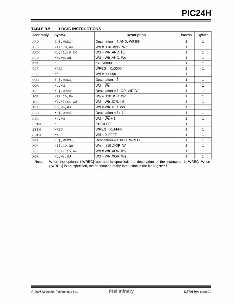
TABLE 9-5: LOGIC INSTRUCTIONSAssembly Syntax Description Words CyclesAND f {,WREG} Destination = f .AND. WREG 1 1AND #lit10,Wn Wn = lit10 .AND. Wn 1 1AND Wb,#lit5,Wd Wd = Wb .AND. lit5 1 1AND Wb,Ws,Wd Wd = Wb .AND. Ws 1 1CLR f f = 0x0000 1 1CLR WREG WREG = 0x0000 1 1CLR Wd Wd = 0x0000 1 1
COM f {,WREG} Destination = f 1 1
COM Ws,Wd Wd = Ws 1 1IOR f {,WREG} Destination = f .IOR. WREG 1 1IOR #lit10,Wn Wn = lit10 .IOR. Wn 1 1IOR Wb,#lit5,Wd Wd = Wb .IOR. lit5 1 1IOR Wb,Ws,Wd Wd = Wb .IOR. Ws 1 1
NEG f {,WREG} Destination = f + 1 1 1
NEG Ws,Wd Wd = Ws + 1 1 1SETM f f = 0xFFFF 1 1SETM WREG WREG = 0xFFFF 1 1SETM Wd Wd = 0xFFFF 1 1XOR f {,WREG} Destination = f .XOR. WREG 1 1XOR #lit10,Wn Wn = lit10 .XOR. Wn 1 1XOR Wb,#lit5,Wd Wd = Wb .XOR. lit5 1 1XOR Wb,Ws,Wd Wd = Wb .XOR. Ws 1 1
Note: When the optional {,WREG} operand is specified, the destination of the instruction is WREG. When{,WREG} is not specified, the destination of the instruction is the file register f.
© 2005 Microchip Technology Inc. Preliminary DS70166A-page 29

PIC24H
TABLE 9-6: ROTATE/SHIFT INSTRUCTIONSTABLE 9-7: BIT INSTRUCTIONS
Assembly Syntax Description Words Cycles
ASR f {,WREG} Destination = arithmetic right shift f 1 1ASR Ws,Wd Wd = arithmetic right shift Ws 1 1ASR Wb,#lit4,Wnd Wnd = arithmetic right shift Wb by lit4 1 1ASR Wb,Wns,Wnd Wnd = arithmetic right shift Wb by Wns 1 1LSR f {,WREG} Destination = logical right shift f 1 1LSR Ws,Wd Wd = logical right shift Ws 1 1LSR Wb,#lit4,Wnd Wnd = logical right shift Wb by lit4 1 1LSR Wb,Wns,Wnd Wnd = logical right shift Wb by Wns 1 1RLC f {,WREG} Destination = rotate left through Carry f 1 1RLC Ws,Wd Wd = rotate left through Carry Ws 1 1RLNC f {,WREG} Destination = rotate left (no Carry) f 1 1RLNC Ws,Wd Wd = rotate left (no Carry) Ws 1 1RRC f {,WREG} Destination = rotate right through Carry f 1 1RRC Ws,Wd Wd = rotate right through Carry Ws 1 1RRNC f {,WREG} Destination = rotate right (no Carry) f 1 1RRNC Ws,Wd Wd = rotate right (no Carry) Ws 1 1SL f {,WREG} Destination = left shift f 1 1SL Ws,Wd Wd = left shift Ws 1 1SL Wb,#lit4,Wnd Wnd = left shift Wb by lit4 1 1SL Wb,Wns,Wnd Wnd = left shift Wb by Wns 1 1
Note: When the optional {,WREG} operand is specified, the destination of the instruction is WREG. When{,WREG} is not specified, the destination of the instruction is the file register f.
Assembly Syntax Description Words Cycles
BCLR f,#bit4 Bit clear f 1 1BCLR Ws,#bit4 Bit clear Ws 1 1BSET f,#bit4 Bit set f 1 1BSET Ws,#bit4 Bit set Ws 1 1BSW.C Ws,Wb Write C bit to Ws<Wb> 1 1
BSW.Z Ws,Wb Write SZ bit to Ws<Wb> 1 1BTG f,#bit4 Bit toggle f 1 1BTG Ws,#bit4 Bit toggle Ws 1 1BTST f,#bit4 Bit test f 1 1BTST.C Ws,#bit4 Bit test Ws to C 1 1BTST.Z Ws,#bit4 Bit test Ws to SZ 1 1BTST.C Ws,Wb Bit test Ws<Wb> to C 1 1BTST.Z Ws,Wb Bit test Ws<Wb> to SZ 1 1BTSTS f,#bit4 Bit test f then set f 1 1BTSTS.C Ws,#bit4 Bit test Ws to C then set Ws 1 1BTSTS.Z Ws,#bit4 Bit test Ws to SZ then set Ws 1 1FBCL Ws,Wnd Find bit change from left (MSb) side 1 1FF1L Ws,Wnd Find first one from left (MSb) side 1 1FF1R Ws,Wnd Find first one from right (LSb) side 1 1
Note: Bit positions are specified by bit4 (0:15) for word operations.
DS70166A-page 30 Preliminary © 2005 Microchip Technology Inc.

PIC24H
TABLE 9-8: COMPARE/SKIP INSTRUCTIONSAssembly Syntax Description Words CyclesBTSC f,#bit4 Bit test f, skip if clear 1 1 (2 or 3)BTSC Ws,#bit4 Bit test Ws, skip if clear 1 1 (2 or 3)BTSS f,#bit4 Bit test f, skip if set 1 1 (2 or 3)BTSS Ws,#bit4 Bit test Ws, skip if set 1 1 (2 or 3)CP f Compare (f – WREG) 1 1CP Wb,#lit5 Compare (Wb – lit5) 1 1CP Wb,Ws Compare (Wb – Ws) 1 1CP0 f Compare (f – 0x0000) 1 1CP0 Ws Compare (Ws – 0x0000) 1 1
CPB f Compare with Borrow (f – WREG – C) 1 1
CPB Wb,#lit5 Compare with Borrow (Wb – lit5 – C) 1 1
CPB Wb,Ws Compare with Borrow (Wb – Ws – C) 1 1CPSEQ Wb,Wn Compare Wb with Wn, Skip if Equal (Wb = Wn) 1 1 (2 or 3)CPSGT Wb,Wn Signed Compare Wb with Wn, Skip if Greater Than (Wb > Wn) 1 1 (2 or 3)CPSLT Wb,Wn Signed Compare Wb with Wn, Skip if Less Than (Wb < Wn) 1 1 (2 or 3)CPSNE Wb,Wn Signed Compare Wb with Wn, Skip if Not Equal (Wb ≠ Wn) 1 1 (2 or 3)Note 1: Bit positions are specified by bit4 (0:15) for word operations.
2: Conditional skip instructions execute in 1 cycle if the skip is not taken, 2 cycles if the skip is taken over a one-word instruction and 3 cycles if the skip is taken over a two-word instruction.
© 2005 Microchip Technology Inc. Preliminary DS70166A-page 31

PIC24H
TABLE 9-9: PROGRAM FLOW INSTRUCTIONSAssembly Syntax Description Words CyclesBRA Expr Branch unconditionally 1 2BRA Wn Computed branch 1 2BRA C,Expr Branch if Carry (no Borrow) 1 1 (2)BRA GE,Expr Branch if greater than or equal 1 1 (2)BRA GEU,Expr Branch if unsigned greater than or equal 1 1 (2)BRA GT,Expr Branch if greater than 1 1 (2)BRA GTU,Expr Branch if unsigned greater than 1 1 (2)BRA LE,Expr Branch if less than or equal 1 1 (2)BRA LEU,Expr Branch if unsigned less than or equal 1 1 (2)BRA LT,Expr Branch if less than 1 1 (2)BRA LTU,Expr Branch if unsigned less than 1 1 (2)BRA N,Expr Branch if Negative 1 1 (2)BRA NC,Expr Branch if not Carry (Borrow) 1 1 (2)BRA NN,Expr Branch if not Negative 1 1 (2)BRA NOV,Expr Branch if not Overflow 1 1 (2)BRA NZ,Expr Branch if not Zero 1 1 (2)BRA OA,Expr Branch if Accumulator A Overflow 1 1 (2)BRA OB,Expr Branch if Accumulator B Overflow 1 1 (2)BRA OV,Expr Branch if Overflow 1 1 (2)BRA SA,Expr Branch if Accumulator A Saturate 1 1 (2)BRA SB,Expr Branch if Accumulator B Saturate 1 1 (2)BRA Z,Expr Branch if Zero 1 1 (2)CALL Expr Call subroutine 2 2CALL Wn Call indirect subroutine 1 2GOTO Expr Go to address 2 2GOTO Wn Go to address indirectly 1 2RCALL Expr Relative call 1 2RCALL Wn Computed call 1 2REPEAT #lit14 Repeat next instruction (lit14 + 1) times 1 1REPEAT Wn Repeat next instruction (Wn + 1) times 1 1RETFIE Return from interrupt enable 1 3 (2)RETLW #lit10,Wn Return with lit10 in Wn 1 3 (2)RETURN Return from subroutine 1 3 (2)Note 1: Conditional branch instructions execute in 1 cycle if the branch is not taken, or 2 cycles if the branch is
taken. 2: RETURN normally executes in 3 cycles; however, it executes in 2 cycles if an interrupt is pending.
DS70166A-page 32 Preliminary © 2005 Microchip Technology Inc.

PIC24H
TABLE 9-10: SHADOW/STACK INSTRUCTIONSTABLE 9-11: CONTROL INSTRUCTIONS
Assembly Syntax Description Words Cycles
LNK #lit14 Link Frame Pointer 1 1POP f Pop TOS to f 1 1POP Wd Pop TOS to Wd 1 1POP.D Wnd Double pop from TOS to Wnd:Wnd + 1 1 2POP.S Pop shadow registers 1 1PUSH f Push f to TOS 1 1PUSH Ws Push Ws to TOS 1 1PUSH.D Wns Push double Wns:Wns + 1 to TOS 1 2PUSH.S Push shadow registers 1 1ULNK Unlink Frame Pointer 1 1
Assembly Syntax Description Words Cycles
CLRWDT Clear Watchdog Timer 1 1DISI #lit14 Disable interrupts for (lit14 + 1) instruction cycles 1 1NOP No operation 1 1NOPR No operation 1 1PWRSAV #lit1 Enter Power-Saving mode lit1 1 1RESET Software device Reset 1 1
© 2005 Microchip Technology Inc. Preliminary DS70166A-page 33

PIC24H
10.0 MICROCHIP DEVELOPMENT TOOL SUPPORT
Microchip offers comprehensive development toolsand libraries to support the dsPIC30F, dsPIC33F andPIC24H architectures. In addition, the company ispartnering with many third party tools manufacturers foradditional device support. Table 10-1 lists developmenttools that support the PIC24H family. The paragraphsthat follow describe each of the tools in more detail.
TABLE 10-1: PIC24H DEVELOPMENT TOOLSDevelopment Tool Description Part # From
Esse
ntia
l So
ftwar
e To
ols
MPLAB® IDE (see Section 10.1 MPLAB Inte-grated Development Environment Software)
Integrated Development Environment SW007002 Microchip
MPLAB ASM30(see Section 10.2 MPLAB ASM30 Assembler/Linker/Librarian)
Assembler (included in MPLAB IDE) SW007002 Microchip
MPLAB SIM(see Section 10.3 MPLAB SIM Software Simulator)
Software Simulator (Included in MPLAB IDE) SW007002 Microchip
MPLAB VDI(see Section 10.4 MPLAB Visual Device Initializer)
Visual Device Initializer for PIC24H(included in MPLAB IDE)
SW007002 Microchip
MPLAB C30(see Section 10.5 MPLAB C30 C Compiler/Linker/Librarian)
ANSI C Compiler, Assembler, Linker and Librarian SW006012 Microchip
Esse
ntia
l H
ardw
are
Tool
s
MPLAB ICD 2(see Section 10.6 MPLAB ICD 2 In-Circuit Debugger)
In-Circuit Debugger and Device Programmer DV164005 Microchip
MPLAB PM3(see Section 10.7 MPLAB PM3 Universal Device Programmer)
Full-Featured Device Programmer, Base Unit DV007004 MicrochipSocket Module for 100L TQFP Devices (14 mm x 14 mm) TBD MicrochipSocket Module for 80L TQFP Devices (12 mm x 12 mm) TBD MicrochipSocket Module for 64L TQFP Devices (10 mm x 10 mm) TBD Microchip
Legend: TBD = To Be Determined
DS70166A-page 34 Preliminary © 2005 Microchip Technology Inc.
PIC24H
10.1 MPLAB Integrated DevelopmentEnvironment SoftwareThe MPLAB Integrated Development Environment(IDE) is available at no cost. The MPLAB IDE lets theuser edit, compile and emulate from a single userinterface, as depicted in Figure 10-1. Code can bedesigned and developed for the dsPIC DSC devices inthe same design environment as the PICmicromicrocontrollers. The MPLAB IDE is a 32-bit Windows®
operating system-based application that providesmany advanced features for the demanding engineer ina modern, easy-to-use interface. MPLAB IDEintegrates:
• Full-featured, color coded text editor• Easy to use project manager with visual display• Source level debugging• Enhanced source level debugging for ‘C’
(structures, automatic variables, etc.)• Customizable toolbar and key mapping• Dynamic status bar displays processor condition
• Context sensitive, interactive on-line help• Integrated MPLAB SIM instruction simulator• User interface for MPLAB PM3 and PICSTART®
Plus device programmers (sold separately)• User interface for MPLAB ICD 2 In-Circuit
Debugger (sold separately)
The MPLAB IDE allows:
• Editing of source files in either assembly or ‘C’• One-touch compiling and downloading to dsPIC
DSC emulator or simulator• Debugging using:
- Source files- Machine code- Mixed mode source and machine code
The ability to use the MPLAB IDE with multipledevelopment and debugging targets provides easytransition from the cost-effective simulator to MPLABICD 2, or to a full-featured emulator with minimalretraining.
FIGURE 10-1: MPLAB® IDE DESKTOP
Powerful Project Manager handles
multiple projects and all file types
Color keyed editor makes
source code debug easier
Status bar updates on
single step or run
Set break/trace points with
a click of the mouse
Fully customizable watch windows
to view and modify registers and
memory locations
Simply move your mouse over a
variable to view or modify
© 2005 Microchip Technology Inc. Preliminary DS70166A-page 35

PIC24H
10.2 MPLAB ASM30 Assembler/Linker/LibrarianMPLAB ASM30 is a full-featured macro assembler.User-defined macros, conditional assembly and avariety of assembler directives make the MPLABASM30 a powerful code generation tool.
The accompanying MPLAB LINK30 Linker and MPLABLIB30 Librarian modules allow efficient linking, librarycreation and maintenance.
Notable features of the assembler include:
• Support for the entire dsPIC DSC instruction set• Support for fixed-point and floating-point data• Available for Windows operating system• Command Line Interface• Rich Directive Set• Flexible Macro Language• MPLAB IDE compatibility
Notable features of the linker include:
• Automatic or user-defined stack allocation• Supports dsPIC DSC Program Space Visibility
(PSV) window• Available for Windows operating systems• Command Line Interface• Linker scripts for all dsPIC DSC devices• MPLAB IDE compatibility
10.3 MPLAB SIM Software SimulatorThe MPLAB SIM software simulator provides codedevelopment for the PIC24H family in a PC-hostedenvironment by simulating the PIC24H device on aninstruction level. On any instruction, you can examineor modify the data areas and apply stimuli to any of thepins from a file or by pressing a user-defined key.
The execution can be performed in Single-Step,Execute-Until-Break or Trace mode. The MPLAB SIMsoftware simulator fully supports symbolic debuggingusing the MPLAB C30 C compiler and assembler. Thesoftware simulator gives you the flexibility to developand debug code outside of the laboratory environment,making it an excellent multi-project softwaredevelopment tool. Complex stimuli can be injected fromfiles, synchronous clocks or user-defined keys. Outputfiles log register activity for sophisticated post analysis.
Besides modeling the behavior of the CPU, MPLABSIM also supports the following peripherals:
10.4 MPLAB Visual Device Initializer The MPLAB Visual Device Initializer (VDI) simplifiesthe task of configuring the PIC24H. MPLAB VDIsoftware allows you to configure the entire processorgraphically (see Figure 10-2). And when you’re done, amouse click generates your code in assembly or‘C’ code. MPLAB VDI performs extensive errorchecking on assignments and conflicts on pins,memories and interrupts, as well as selection ofoperating conditions. Generated code files areintegrated seamlessly with the rest of our applicationcode through MPLAB Project.
Detailed resource assignment and configurationreports simplify project documentation. Key features ofMPLAB VDI include:
• Drag-and-drop feature selection• One click configuration• Extensive error checking• Generates initialization code in the form of a
‘C’ callable assembly function• Integrates seamlessly in MPLAB Project• Printed reports ease project documentation
requirements• MPLAB Visual Device Initializer is an MPLAB
plug-in and can be installed independently of MPLAB IDE
FIGURE 10-2: MPLAB® VDI DISPLAY
• Timers • Motor Control PWM• Input Capture • UART• 12-Bit ADC • I/O Ports• 10-Bit ADC • Program Flash
DS70166A-page 36 Preliminary © 2005 Microchip Technology Inc.

PIC24H
10.5 MPLAB C30 C Compiler/Linker/Librarian The Microchip Technology MPLAB C30 C Compilerprovides ‘C’ language support for the PIC24H family.This C compiler is a fully ANSI-compliant product withstandard libraries. It is highly optimized for the PIC24Hfamily and takes advantage of many PIC24Harchitecture-specific features to help you generate veryefficient software code. Figure 10-3 illustrates the codesize efficiency relative to several competitors.
MPLAB C30 also provides extensions that allow forexcellent support of the hardware, such as interruptsand peripherals. It is fully integrated with MPLAB IDEfor high-level source debugging.
The MPLAB C30 has these characteristics:
• 16-bit native data types• Efficient use of register-based, 3-operand
instructions• Complex addressing modes• Efficient multi-bit shift operations• Efficient signed/unsigned comparisons
MPLAB C30 comes complete with its own assembler,linker and librarian. These allow Mixed mode ‘C’ andassembly programs and link the resulting object filesinto a single executable file. The compiler is soldseparately. The assembler, linker and librarian areavailable for free with MPLAB C30.
MPLAB C30 also includes the Math Library, PeripheralLibrary and standard ‘C’ libraries.
FIGURE 10-3: RELATIVE CODE SIZE (IN BYTES)
© 2005 Microchip Technology Inc. Preliminary DS70166A-page 37

PIC24H
10.6 MPLAB ICD 2 In-Circuit DebuggerThe MPLAB ICD 2 In-Circuit Debugger is a powerful,low-cost, run-time development tool that uses in-circuitdebugging capability built into the PIC24H Flashdevices. This feature, along with Microchip’s In-CircuitSerial Programming™ (ICSP™) protocol, gives youcost-effective, in-circuit debugging from the graphicaluser interface of MPLAB IDE. It lets you develop anddebug source code by watching variables, single-stepping and setting breakpoints, as well as running atfull speed to test hardware in real time.The MPLAB ICD 2 has these features:
• Full-speed operation to the range of the device• Serial or USB PC connector• USB-powered from PC interface• Low noise power (VPP and VDD) for use with
analog and other noise sensitive applications• Operation down to 2.0V• Can be used as debugger and inexpensive serial
programmer• Some device resources required (80 bytes of
RAM and 2 pins)
FIGURE 10-4: MPLAB® ICD 2 IN-CIRCUIT DEBUGGER
10.7 MPLAB PM3 Universal Device Programmer
The MPLAB PM3 Universal Device Programmer is easyto use with a PC, or as a stand-alone unit, to programMicrochip’s entire line of PICmicro MCU devices as wellas the latest PIC24H DSC devices. The MPLAB PM3features a large and bright LCD unit (128 x 64 pixels) todisplay easy menus, programming statistics and statusinformation.
The MPLAB PM3 programmer has exceptionalprogramming speed for high production throughput,especially important for large memory devices. It alsoincludes a Secure Digital/Multimedia Card slot for easyand secure data storage and transfer.
The MPLAB PM3 programmer is designed with40 programmable socket pins and therefore, eachsocket module can be configured to support manydifferent devices. As a result, fewer socket modules arerequired to support the entire line of Microchip parts.The socket modules use multi-pin connectors for highreliability and quick interchange.
When connected to a PC host system, the MPLABPM3 programmer is seamlessly integrated with theMPLAB Integrated Development Environment (IDE),providing a user-friendly programming interface.
Key features of the MPLAB PM3 Programmer include:
• RS-232 or USB interface• Integrated In-Circuit Serial Programming (ICSP)
interface• Fast programming time• Three operating modes:
- PC Host mode for full control- Safe mode for secure data- Stand-Alone mode for programming without
a PC• Complete line of interchangeable socket modules
to support all Microchip devices and package options (sold separately)
• SQTPSM serialization for programming unique serial numbers while in PC Host mode.
• An alternate DOS command line interface for batch control
• Large easy-to-read display• Field upgradeable firmware allows quick new
device support• Secure Digital (SD) and Multimedia Card (MMC)
external memory support• Buzzer notification for noisy environments
FIGURE 10-5: MPLAB® PM3 DEVICE PROGRAMMER
DS70166A-page 38 Preliminary © 2005 Microchip Technology Inc.

PIC24H
11.0 PIC24H DEVELOPMENT TOOLS AND APPLICATION LIBRARIES
Microchip offers a comprehensive set of tools andlibraries to help with rapid development of PIC24Hdevice-based application(s).
Table 11-1 summarizes available and planned PIC24Hsoftware tools and libraries. Microchip also providesvalue added services, such as skilled/certifiedtechnical application contacts, reference designs andhardware and software developers. (Contact MicrochipDSCD Marketing for availability.)
TABLE 11-1: MICROCHIP SOFTWARE DEVELOPMENT TOOLS AND APPLICATION LIBRARIESDevelopment Tool Description Part #
Math Library (see Section 11.1 Math Library)
Double Precision and Floating-Point Library (ASM, C Wrapper)
SW300020
Peripheral Library (see Section 11.2 Peripheral Driver Library)
Peripheral Initialization, Control and Utility Routines (C) SW300021
dsPICworks™ Tool (see Section 11.3 dsPICworks™ Data Analysis Tool and DSP Software)
Graphical Data Analysis and Conversion Tool for DSP Algorithms SW300023
TCP/IP Library (see Section 11.4 Microchip TCP/IP Stack)
TCP/IP Connectivity and Protocol Support SW300024
© 2005 Microchip Technology Inc. Preliminary DS70166A-page 39

PIC24H
11.1 Math LibraryThe PIC24H Math Library is the compiled version of themath library that is distributed with the highly optimized,ANSI-compliant PIC24H MPLAB C30 C Compiler(SW006012). It contains advanced single and double-precision floating-point arithmetic and trigonometricfunctions from the standard ‘C’ header file (math.h).The library delivers small program code size and datasize, reduced cycles and high accuracy.Features• The math library is callable from either MPLAB
C30 or PIC24H assembly language.• The functions are IEEE-754 compliant, with
signed zero, signed infinity, NaN (Not a Number) and denormal support and operated in the “Round to Nearest” mode.
• Compatible with MPLAB ASM30 and MPLAB LINK30, which are available at no charge from Microchip’s web site.
Table 11-2 shows the memory usage and performanceof the Math Library. Table 11-3 lists the math functionsthat are included.
TABLE 11-2: MEMORY USAGE AND PERFORMANCE
TABLE 11-3: MATH FUNCTIONS
Memory Usage (bytes)(1,2)
Code size 5250Data size 4
Performance (cycles)(1,3)
add 122sub 124mul 109div 361rem 385sqrt 492Note 1: Results are based on using PIC24H
MPLAB C30 C Compiler (SW006012), version 1.20.
2: Maximum “Memory Usage” when all functions in the library are loaded. Most applications will use less.
3: Average 32-bit floating-point performance results.
Single and Double-Precision Floating-Point Functions
Arithmetic Functions add, subtract, multiply, divide, remainderRoot and Power Functions pow, sqrtTrigonometric and Hyperbolic Functions acos, asin, atan, atan2, cos, cosh, sin, sinh, tan, tanhLogarithmic and Exponential Functions exp, log, log10, frexp, ldexpRounding Functions ceil, floorAbsolute Value Functions fabsModular Arithmetic Functions fmod, modfComparison and Conversions comparison, integer and floating-point conversions
DS70166A-page 40 Preliminary © 2005 Microchip Technology Inc.

PIC24H
11.2 Peripheral Driver LibraryMicrochip offers a free peripheral driver library thatsupports the setup and control of PIC24H hardwareperipherals, including, but not limited to:• Analog-to-Digital Converter• UART• SPI• I2C• General-purpose Timers• Input Capture• Output Compare/Simple PWM• CAN• I/O Ports and External Interrupts• Reset
In addition to the hardware peripherals, the librarysupports software generated peripherals, such asstandard LCD drivers, which support an Hitachi stylecontroller.
The peripheral library consist of more than 270functions, as well as several macros for simple taskssuch as enabling and disabling interrupts. All peripheraldriver routines are developed and optimized using theMPLAB C30 C Compiler. Electronic documentationaccompanies the peripheral library to help you becomefamiliar with and implement the library functions.
Key features of the PIC24H Peripheral Library include:
• A library file for each individual device from the PIC24H family, including functions corresponding to peripherals present in that particular device.
• ‘C’ include files that let you take advantage of predefined constants for passing parameters to various library functions. There is an include file for each peripheral module.
• Since the functions are in the form of precompiled libraries, they can be called from a user application program written in either MPLAB C30 C Compiler or PIC24H assembly language.
• Included ‘C’ source code allows you to customize peripheral functions to suit your specific application requirements.
• Predefined constants in the ‘C’ include files eliminate the need to refer to the details and structure of every Special Function Register while initializing peripherals or checking status bits.
11.3 dsPICworks™ Data Analysis Tool and DSP Software
The dsPICworks tool is a free data analysis and signalprocessing package for use with Microsoft®Windows® 9x, Windows NT®, Windows 2000 andWindows XP platforms. It provides an extensivenumber of functions encompassing:
• Wide variety of Signal Generators – Sine, Square, Triangular, Window Functions, Noise
• Extensive DSP Functions – FFT, DCT, Filtering, Convolution, Interpolation
• Extensive Arithmetic Functions – Algebraic Expressions, Data Scaling, Clipping, etc.
• 1-D, 2-D and 3-D Displays• Multiple Data Quantization and Saturation
Options• Multi-Channel Data Support• Automatic “Script File”-based Execution Options
available for any user-defined sequence of dsPICworks Tool Functions
• File Import/Export interoperable with MPLAB IDE• Digital Filtering Options support Filters generated
by dsPIC DSC Filter Design• ASM30 Assembler File Option to export Data
Tables into PIC24H RAM
FIGURE 11-1: dsPICworks™ DATA ANALYSIS TOOL AND DSP SOFTWARE
© 2005 Microchip Technology Inc. Preliminary DS70166A-page 41

PIC24H
11.3.1 SIGNAL GENERATIONdsPICworks Data Analysis Tool and DSP Softwaresupport an extensive set of signal generators, includingbasic sine, square and triangle wave generators, as wellas advanced generators for window functions, unit step,unit sample, sine, exponential and noise functions.Noise, with specified distribution, can be added to anysignal. Signals can be generated as 32-bit floating-point,or as 16-bit fractional fixed-point values, for any desiredsampling rate. The length of the generated signal islimited only by available disk space. Signals can beimported or exported from or to MPLAB IDE file registerwindows. Multi-channel data can be created by a set ofmultiplexing functions.11.3.2 DIGITAL SIGNAL PROCESSING (DSP) AND ARITHMETIC OPERATIONS
dsPICworks Data Analysis Tool and DSP Softwarehave a wide range of DSP and arithmetic functions thatcan be applied to signals. Standard DSP functionsinclude transform operations: FFT and DCT,convolution and correlation, signal decimation, signalinterpolation sample rate conversion and digitalfiltering. Digital filtering is an important part of thedsPICworks tool. It uses filters designed by the sister-application, dsPIC DSC Filter Design, and applies themto synthesized or imported signals. The dsPICworkstool also features special operations, such as signalclipping, scaling and quantization, all of which are vitalin real practical analysis of DSP algorithms.
11.3.3 DISPLAY AND MEASUREMENTdsPICworks Data Analysis Tool and DSP Softwarehave a wide variety of display and measurementoptions. Frequency domain data may be plotted in theform of 2-dimensional ‘spectrogram’ and 3-dimensional‘waterfall’ options. The signals can be measuredaccurately by a simple mouse click. The log windowshows current cursor coordinates, as well as derivedvalues, such as the difference from last position andsignal frequency. Signal strength can be measuredover a particular range of frequencies. Special supportalso exists for displaying multi-channel and multiplexeddata. Graphs allow zoom options. The user can choosefrom a set of color scheme options to customize displaysettings.
11.3.4 FILE IMPORT/EXPORT – MPLAB IDE AND MPLAB ASM30 SUPPORT
dsPICworks Data Analysis Tool and DSP Softwareallow data to be imported from the external world in theform of ASCII text or binary files. Conversely, it alsoallows data to be exported out in the form of files. ThedsPICworks tool supports all file formats supported bythe MPLAB import/export table. This feature allows theuser to bring real-world data from MPLAB IDE into thedsPICworks tool for analysis. The dsPICworks tool canalso create ASM30 assembler files that can beincluded into the MPLAB workspace.
11.4 Microchip TCP/IP StackThe free Microchip TCP/IP Stack is a suite of programsthat can provide services to standard (HTTP Server,Mail Client, etc.) or custom TCP/IP-based applications.Users do not need to be an expert in TCP/IPspecifications to use it and only need specificknowledge of TCP/IP in the accompanying HTTPServer application.
This stack is implemented in a modular fashion, with allof its services creating highly abstracted layers, eachlayer accessing services from one or more layersdirectly below it. The stack is optimized for size and isdesigned to run on the PIC24H using thedsPICDEM.net™ Development Board; however, it canbe easily retargeted to any hardware equipped with aPIC24H. HTML web pages generated by the PIC24Hcan be viewed with a standard web browser such asMicrosoft Internet Explorer.
Key features of the Microchip TCP/IP Stack include:
• Out-of-box support for Microchip C30 C Compiler• Implements complete TCP state machine• Multiple TCP and UDP sockets with simultaneous
connection/management• Includes modules supporting various standard
protocols: MAC, SLIP, ARP, IP, ICMP, TCP, SNMP, UDP, DHCP, FTP, IP Gleaning, HTTP, MPFS (Microchip File System)
• Can be used as a part of the HTTP Server (included) or any custom TCP/IP-based application
• RTOS independent
DS70166A-page 42 Preliminary © 2005 Microchip Technology Inc.

PIC24H
12.0 THIRD PARTY DEVELOPMENT TOOLS AND APPLICATION LIBRARIES
Besides providing development tools and applicationlibraries for PIC24H products, Microchip also partnerswith key third party tool manufacturers to developquality hardware and software tools in support of thePIC24H product family. Details of various third partydevelopment tools will be provided shortly.
© 2005 Microchip Technology Inc. Preliminary DS70166A-page 43

PIC24H
13.0 PIC24H HARDWARE DEVELOPMENT BOARDS
Microchip initially offers two hardware developmentboards that help you quickly prototype and validate keyaspects of your design. Each board features variousPIC24H peripherals and supports Microchip’s MPLAB
In-Circuit Debugger (ICD 2) tool for cost-effectivedebugging and programming of the PIC24H devices.These two boards are shown in Table 13-1.
Microchip plans to offer additional hardwaredevelopment boards to support the PIC24H productfamily. Contact Microchip DSCD Marketing foradditional information.
TABLE 13-1: HARDWARE DEVELOPMENT BOARDSDevelopment Tool Description Part # From
Dev
elop
men
t Boa
rds
and
Ref
eren
ce D
esig
ns
General-purpose Development Board
dsPICDEM™ 80-Pin Starter Development Board DM300019 MicrochipExplorer 16 Development Board DM240001 Microchip
Plug
-inSa
mpl
es
Plug-in Sample(see Section 13.3 Plug-in Modules)
PC board with 100-pin PIC24H MCU sample; use with DM240001 development board.
TBD Microchip
PC board with 100-pin PIC24H MCU sample; use with DM300019 development board.
TBD Microchip
Acc
esso
ry
Kits
Acoustic Accessory Kit(see Section 13.3 Plug-in Modules)
Accessory Kit includes: audio cable, headset, oscillators, microphone, speaker, DB9 M/F RS-232 cable, DB9M-DB9M Null Modem Adapter and can be used for library evaluation.
AC300030 Microchip
DS70166A-page 44 Preliminary © 2005 Microchip Technology Inc.

PIC24H
13.1 dsPICDEM™ 80-Pin StarterDevelopment BoardThis development board offers a very economical wayto evaluate both the dsPIC30F and PIC24H General-purpose and Motor Control Family devices. This boardis an ideal prototyping tool to help you quickly developand validate key design requirements.
Some key features and attributes of the dsPICDEM80-Pin Starter Development Board include:
• Includes an 80-pin dsPIC30F6014A plug-in module (MA300014)
• Power input from 9V supply• Selectable voltage regulator outputs of 5V
and 3.3V• LEDs, switches, potentiometer, UART interface• ADC input filter circuit for speech band signal
input• On-board DAC and filter for speech band signal output• Circuit prototyping area• Assembly language demonstration program and
tutorial• Can accommodate 100 to 80-pin adapter PIC24H
plug-in module
FIGURE 13-1: dsPICDEM™ 80-PIN STARTER DEVELOPMENT BOARD
13.2 Explorer 16 Development BoardThis development board offers a very economical wayto evaluate both the PIC24H General-purpose andMotor Control Family devices, as well as the PIC24Fdevices. This board is an ideal prototyping tool to helpyou quickly develop and validate key designrequirements.
Some key features and attributes of the Explorer 16Development Board include:
• Includes a 100-pin PIC24H plug-in module • Includes a 100-pin PIC24 plug-in module • Power input from 9V supply• Modular design for plug-in demonstration boards,
expansion header• ICD 2 and JTAG connection for reprogramming• USB and protocol translation support through
PIC18F4450• RS-232 connection with firmware and driver
support• LED bank for general indication• Serial EEPROM• 16 x 2 alphanumeric LCD• Temperature sensor• Terminal interface program and menu programs
FIGURE 13-2: EXPLORER 16 DEVELOPMENT BOARD
© 2005 Microchip Technology Inc. Preliminary DS70166A-page 45

PIC24H
13.3 Plug-in ModulesThe various PIC24H development boards may use theplug-in modules for the PIC24H silicon devices. Sincethe boards contain device header pins on the PCB,they also are used to provide flexibility for thereplacement of the PIC24H silicon. Plug-in sampletypes will be provided, supporting the 64-pin and 100-pin TQFP package types for General-purpose devicesamples. The use of plug-in samples is considered tobe an interim development board mechanization.13.4 Acoustic Accessory KitThe Acoustic Accessory Kit includes the followingaccessories targeted towards acoustics-orientedapplication development support:
• 6 ft. Stereo Audio Cable• Stereo Headset• Two 14.7456 MHz Oscillators• Clip-on Microphone• Fold-up Speaker• 6 ft. DB9 M/F RS-232 Cable• DB9M-DB9M Null Modem Adapter
DS70166A-page 46 Preliminary © 2005 Microchip Technology Inc.

PIC24H
APPENDIX A: DEVICE I/O PINOUTS AND FUNCTIONS FOR GENERAL-PURPOSE FAMILY
Table A-1 provides a brief description of device I/Opinouts and functions that can be multiplexed to a portpin. Multiple functions may exist on one port pin. Whenmultiplexing occurs, the peripheral module’s functionalrequirements may force an override of the datadirection of the port pin.
TABLE A-1: PINOUT I/O DESCRIPTIONS FOR GENERAL-PURPOSE FAMILY
Pin Name PinType
Input BufferType Description
AN0-AN31 I Analog Analog input channels.AVDD P P Positive supply for analog module.AVSS P P Ground reference for analog module.CLKI
CLKO
I
O
ST/CMOS
—
External clock source input. Always associated with OSC1 pin function.Oscillator crystal output. Connects to crystal or resonator in Crystal Oscillator mode. Optionally functions as CLKO in RC and EC modes. Always associated with OSC2 pin function.
CN0-CN23 I ST Input change notification inputs. Can be software programmed for internal weak pull-ups on all inputs.
COFSCSCKCSDICSDO
I/OI/OIO
STSTST—
Data Converter Interface frame synchronization pin.Data Converter Interface serial clock input/output pin.Data Converter Interface serial data input pin.Data Converter Interface serial data output pin.
C1RXC1TXC2RXC2TX
IOIO
ST—ST—
ECAN1 bus receive pin.ECAN1 bus transmit pin.ECAN2 bus receive pin.ECAN2 bus transmit pin.
PGD1/EMUD1PGC1/EMUC1PGD2/EMUD2PGC2/EMUC2PGD3/EMUD3PGC3/EMUC3
I/OI
I/OI
I/OI
STSTSTSTSTST
Data I/O pin for programming/debugging communication channel 1.Clock input pin for programming/debugging communication channel 1.Data I/O pin for programming/debugging communication channel 2.Clock input pin for programming/debugging communication channel 2.Data I/O pin for programming/debugging communication channel 3.Clock input pin for programming/debugging communication channel 3.
IC1-IC8 I ST Capture inputs 1 through 8.INT0INT1INT2INT3INT4
IIIII
STSTSTSTST
External interrupt 0.External interrupt 1.External interrupt 2.External interrupt 3.External interrupt 4.
MCLR I/P ST Master Clear (Reset) input or programming voltage input. This pin is an active-low Reset to the device.
OCFAOCFBOC1-OC8
IIO
STST—
Compare Fault A input (for Compare Channels 1, 2, 3 and 4).Compare Fault B input (for Compare Channels 5, 6, 7 and 8).Compare outputs 1 through 8.
OSC1
OSC2
I
I/O
ST/CMOS
—
Oscillator crystal input. ST buffer when configured in RC mode; CMOS otherwise.Oscillator crystal output. Connects to crystal or resonator in Crystal Oscillator mode. Optionally functions as CLKO in RC and EC modes.
RA0-RA7RA9-RA10RA12-RA15
I/OI/OI/O
STSTST
PORTA is a bidirectional I/O port.
RB0-RB15 I/O ST PORTB is a bidirectional I/O port.Legend: CMOS = CMOS compatible input or output; Analog = Analog input
ST = Schmitt Trigger input with CMOS levels; O = Output; I = Input; P = Power
© 2005 Microchip Technology Inc. Preliminary DS70166A-page 47

PIC24H
RC1-RC4RC12-RC15
I/OI/O
STST
PORTC is a bidirectional I/O port.
RD0-RD15 I/O ST PORTD is a bidirectional I/O port.RE0-RE9 I/O ST PORTE is a bidirectional I/O port.RF0-RF8 RF12-RF13
I/OI/O
STST
PORTF is a bidirectional I/O port.
RG0-RG3RG6-RG9RG12-RG15
I/OI/OI/O
STSTST
PORTG is a bidirectional I/O port.
SCK1SDI1SDO1SS1SCK2SDI2SDO2SS2
I/OIOI
I/OIOI
STST—STSTST—ST
Synchronous serial clock input/output for SPI1.SPI1 data in.SPI1 data out.SPI1 slave synchronization.Synchronous serial clock input/output for SPI2.SPI2 data in.SPI2 data out.SPI2 slave synchronization.
SCL1SDA1SCL2SDA2
I/OI/OI/OI/O
STSTSTST
Synchronous serial clock input/output for I2C1.Synchronous serial data input/output for I2C1.Synchronous serial clock input/output for I2C2.Synchronous serial data input/output for I2C2.
SOSCISOSCO
IO
ST/CMOS—
32 kHz low-power oscillator crystal input; CMOS otherwise.32 kHz low-power oscillator crystal output.
TMSTCKTDITDO
II/OIO
STSTST—
JTAG Test mode select pin.JTAG test clock input/output pin.JTAG test data input pin.JTAG test data output pin.
T1CKT2CKT3CKT4CKT5CKT6CKT7CKT8CKT9CK
IIIIIIIII
STSTSTSTSTSTSTSTST
Timer1 external clock input.Timer2 external clock input.Timer3 external clock input.Timer4 external clock input.Timer5 external clock input.Timer6 external clock input.Timer7 external clock input.Timer8 external clock input.Timer9 external clock input.
U1CTSU1RTSU1RXU1TXU2CTSU2RTSU2RXU2TX
IOIOIOIO
ST—ST—ST—ST—
UART1 clear to send.UART1 ready to send.UART1 receive.UART1 transmit.UART2 clear to send.UART2 ready to send.UART2 receive.UART2 transmit.
VDD P — Positive supply for peripheral logic and I/O pins.VDDCORE P — CPU logic filter capacitor connection.VSS P — Ground reference for logic and I/O pins.VREF+ I Analog Analog voltage reference (high) input.VREF- I Analog Analog voltage reference (low) input.
TABLE A-1: PINOUT I/O DESCRIPTIONS FOR GENERAL-PURPOSE FAMILY (CONTINUED)
Pin Name PinType
Input BufferType Description
Legend: CMOS = CMOS compatible input or output; Analog = Analog inputST = Schmitt Trigger input with CMOS levels; O = Output; I = Input; P = Power
DS70166A-page 48 Preliminary © 2005 Microchip Technology Inc.

PIC24H
Pin Diagrams (Continued)64-Pin TQFP
12345678910111213 36
353433
32313029282726
64 63 62 61 60 59 58 57 56
141516
17 18 19 20 21 22 23 24 25
PGC2/EMUC2/SOSCO/T1CK/CN0/RC14PGD2/EMUD2/SOSCI/T4CK/CN1/RC13OC1/RD0IC4/INT4/RD11
IC2/U1CTS/INT2/RD9IC1/INT1/RD8VSS
OSC2/CLKO/RC15OSC1/CLKIN/RC12VDD
SCL1/RG2
U1RTS/SCK1/INT0/RF6U1RX/SDI1/RF2U1TX/SDO1/RF3
RG15AN16/T2CK/T7CK/RC1AN17/T3CK/T6CK/RC2
SCK2/CN8/RG6SDI2/CN9/RG7
SDO2/CN10/RG8MCLR
VSS
VDD
AN3/CN5/RB3AN2/SS1/LVDIN/CN4/RB2
PGC3/EMUC3/AN1/VREF-/CN3/RB1PGD3/EMUD3/AN0/VREF+/CN2/RB0
OC
8/C
N16
/RD
7
RG
13R
G12
RG
14
VD
DC
OR
E
RG
1R
F1
RG
0
OC
2/R
D1
OC
3/R
D2
PG
C1/
EM
UC
1/A
N6/
OC
FA/R
B6
PG
D1/
EM
UD
1/A
N7/
RB
7AV
DD
AVS
S
U2C
TS/A
N8/
RB
8A
N9/
RB
9TM
S/A
N10
/RB
10TD
O/A
N11
/RB
11VS
S
VD
D
TCK
/AN
12/R
B12
TDI/A
N13
/RB
13U
2RTS
/AN
14/R
B14
AN
15/O
CFB
/CN
12/R
B15
U2T
X/C
N18
/RF5
U2R
X/C
N17
/RF4
SDA1/RG3
43424140393837
44
484746
50 495154 53 5255
45
SS2/T5CK/CN11/RG9
AN5/IC8/CN7/RB5AN4/IC7/CN6/RB4
IC3/INT3/RD10
VD
D
RF0
OC
4/R
D3
OC
7/C
N15
/RD
6O
C6/
IC6/
CN
14/R
D5
OC
5/IC
5/C
N13
/RD
4
PIC24HJ64GP206PIC24HJ128GP206PIC24HJ256GP206
Note: The PIC24HJ64GP206 device does not have the SCL2 and SDA2 pins.
© 2005 Microchip Technology Inc. Preliminary DS70166A-page 49

PIC24H
Pin Diagrams (Continued)64-Pin TQFP
12345678910111213 36
353433
32313029282726
64 63 62 61 60 59 58 57 56
141516
17 18 19 20 21 22 23 24 25
PGC2/EMUC2/SOSCO/T1CK/CN0/RC14PGD2/EMUD2/SOSCI/T4CK/CN1/RC13OC1/RD0IC4/INT4/RD11
IC2/U1CTS/INT2/RD9IC1/INT1/RD8VSS
OSC2/CLKO/RC15OSC1/CLKIN/RC12VDD
SCL1/RG2
U1RTS/SCK1/INT0/RF6U1RX/SDI1/RF2U1TX/SDO1/RF3
RG15AN16/T2CK/T7CK/RC1AN17/T3CK/T6CK/RC2
SCK2/CN8/RG6SDI2/CN9/RG7
SDO2/CN10/RG8MCLR
VSS
VDD
AN3/CN5/RB3AN2/SS1/LVDIN/CN4/RB2
PGC3/EMUC3/AN1/VREF-/CN3/RB1PGD3/EMUD3/AN0/VREF+/CN2/RB0
OC
8/C
N16
/RD
7
RG
13R
G12
RG
14
VD
DC
OR
E
RG
1R
F1
RG
0
OC
2/R
D1
OC
3/R
D2
PG
C1/
EM
UC
1/A
N6/
OC
FA/R
B6
PG
D1/
EM
UD
1/A
N7/
RB
7AV
DD
AVS
S
U2C
TS/A
N8/
RB
8A
N9/
RB
9TM
S/A
N10
/RB
10TD
O/A
N11
/RB
11V
SS
VD
D
TCK
/AN
12/R
B12
TDI/A
N13
/RB
13U
2RTS
/AN
14/R
B14
AN
15/O
CFB
/CN
12/R
B15
U2T
X/SC
L2/C
N18
/RF5
U2R
X/S
DA
2/C
N17
/RF4
SDA1/RG3
43424140393837
44
484746
50 495154 53 5255
45
SS2/T5CK/CN11/RG9
AN5/IC8/CN7/RB5AN4/IC7/CN6/RB4
IC3/INT3/RD10
VD
D
RF0
OC
4/R
D3
OC
7/C
N15
/RD
6O
C6/
IC6/
CN
14/R
D5
OC
5/IC
5/C
N13
/RD
4
PIC24HJ128GP306
DS70166A-page 50 Preliminary © 2005 Microchip Technology Inc.
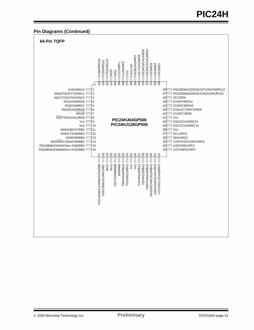
PIC24H
Pin Diagrams (Continued)64-Pin TQFP
12345678910111213 36
353433
32313029282726
64 63 62 61 60 59 58 57 56
141516
17 18 19 20 21 22 23 24 25
PGC2/EMUC2/SOSCO/T1CK/CN0/RC14PGD2/EMUD2/SOSCI/T4CK/CN1/RC13OC1/RD0IC4/INT4/RD11
IC2/U1CTS/INT2/RD9IC1/INT1/RD8VSS
OSC2/CLKO/RC15OSC1/CLKIN/RC12VDD
SCL1/RG2
U1RTS/SCK1/INT0/RF6U1RX/SDI1/RF2U1TX/SDO1/RF3
COFS/RG15AN16/T2CK/T7CK/RC1AN17/T3CK/T6CK/RC2
SCK2/CN8/RG6SDI2/CN9/RG7
SDO2/CN10/RG8MCLR
VSS
VDD
AN3/CN5/RB3AN2/SS1/LVDIN/CN4/RB2
PGC3/EMUC3/AN1/VREF-/CN3/RB1PGD3/EMUD3/AN0/VREF+/CN2/RB0
OC
8/C
N16
/RD
7
CS
DO
/RG
13C
SD
I/RG
12C
SC
K/R
G14
VD
DC
OR
E
RG
1C
1TX
/RF1
RG
0
OC
2/R
D1
OC
3/R
D2
PG
C1/
EM
UC
1/A
N6/
OC
FA/R
B6
PG
D1/
EM
UD
1/A
N7/
RB
7AV
DD
AVS
S
U2C
TS/A
N8/
RB
8A
N9/
RB
9TM
S/A
N10
/RB
10TD
O/A
N11
/RB
11V S
S
VDD
TCK
/AN
12/R
B12
TDI/A
N13
/RB
13U
2RTS
/AN
14/R
B14
AN
15/O
CFB
/CN
12/R
B15
U2T
X/S
CL2
/CN
18/R
F5U
2RX
/SD
A2/
CN
17/R
F4
SDA1/RG3
43424140393837
44
484746
50 495154 53 5255
45
SS2/T5CK/CN11/RG9
AN5/IC8/CN7/RB5AN4/IC7/CN6/RB4
IC3/INT3/RD10
VD
D
C1R
X/R
F0
OC
4/R
D3
OC
7/C
N15
/RD
6O
C6/
IC6/
CN
14/R
D5
OC
5/IC
5/C
N13
/RD
4
PIC24HJ64GP506PIC24HJ128GP506
© 2005 Microchip Technology Inc. Preliminary DS70166A-page 51

PIC24H
Pin Diagrams (Continued)9294 93 91 90 89 88 87 86 85 84 83 82 81 80 79 78
20
2345678910111213141516
65646362616059
26
56
4544434241403928 29 30 31 32 33 34 35 36 37 38
171819
2122
951
7677
72717069686766
757473
5857
2423
25
9698 979927 46 47 48 49 50
5554535251
OC6/
CN14
/RD5
OC5/
CN13
/RD4
IC6/
CN19
/RD1
3IC
5/RD
12OC
4/RD
3OC
3/RD
2OC
2/RD
1
AN23
/CN2
3/RA
7AN
22/C
N22/
RA6
AN26
/RE2
RG13
RG12
RG14
AN25
/RE1
AN24
/RE0
RG0
AN28
/RE4
AN27
/RE3
RF0
VDDC
ORE
PGD2/EMUD2/SOSCI/CN1/RC13OC1/RD0
IC3/RD10IC2/RD9IC1/RD8
IC4/RD11
SDA2/RA3SCL2/RA2
OSC2/CLKO/RC15OSC1/CLKIN/RC12VDD
SCL1/RG2
SCK1/INT0/RF6SDI1/RF7SDO1/RF8
SDA1/RG3
U1RX/RF2U1TX/RF3
VSS
PGC2/EMUC2/SOSCO/T1CK/CN0/RC14
VREF
+/RA
10VR
EF-/R
A9
AVDD
AVSS
AN8/
RB8
AN9/
RB9
AN10
/RB1
0AN
11/R
B11
V DD
U2CT
S/RF
12U2
RTS/
RF13
IC7/
U1CT
S/CN
20/R
D14
IC8/
U1RT
S/CN
21/R
D15
V DD
VSS
PGC1
/EM
UC1/
AN6/
OCF
A/RB
6PG
D1/E
MUD
1/AN
7/RB
7
U2TX
/CN1
8/RF
5U2
RX/C
N17/
RF4
AN29/RE5AN30/RE6AN31/RE7
AN16/T2CK/T7CK/RC1AN17/T3CK/T6CK/RC2AN18/T4CK/T9CK/RC3AN19/T5CK/T8CK/RC4
SCK2/CN8/RG6
VDD
TMS/RA0AN20/INT1/RE8AN21/INT2/RE9
AN5/CN7/RB5AN4/CN6/RB4AN3/CN5/RB3
AN2/SS1/LVDIN/CN4/RB2
SDI2/CN9/RG7SDO2/CN10/RG8
PGC3/EMUC3/AN1/CN3/RB1PGD3/EMUD3/AN0/CN2/RB0
RG15VDD
SS2/CN11/RG9MCLR
AN12
/RB1
2AN
13/R
B13
AN14
/RB1
4AN
15/O
CFB/
CN12
/RB1
5
RG1
RF1
OC8/
CN16
/RD7
OC7/
CN15
/RD6
TDO/RA5
INT4/RA15INT3/RA14
VSS
VSS
VSS
VDD
TDI/RA4
TCK/
RA1
100-Pin TQFP
PIC24HJ64GP210PIC24HJ128GP210
100
PIC24HJ128GP310PIC24HJ256GP210
DS70166A-page 52 Preliminary © 2005 Microchip Technology Inc.

PIC24H
Pin Diagrams (Continued)9294 93 91 90 89 88 87 86 85 84 83 82 81 80 79 78
20
2345678910111213141516
65646362616059
26
56
4544434241403928 29 30 31 32 33 34 35 36 37 38
171819
2122
95
1
7677
72717069686766
757473
5857
2423
25
9698 979927 46 47 48 49 50
5554535251
OC
6/C
N14
/RD
5O
C5/
CN
13/R
D4
IC6/
CN
19/R
D13
IC5/
RD
12O
C4/
RD
3O
C3/
RD
2O
C2/
RD
1
AN23
/CN
23/R
A7AN
22/C
N22
/RA6
AN26
/RE2
RG
13R
G12
RG
14AN
25/R
E1AN
24/R
E0
RG
0
AN28
/RE4
AN27
/RE3
C1R
X/R
F0
V DD
CO
RE
PGD2/EMUD2/SOSCI/CN1/RC13OC1/RD0
IC3/RD10IC2/RD9IC1/RD8
IC4/RD11
SDA2/RA3SCL2/RA2
OSC2/CLKO/RC15OSC1/CLKIN/RC12VDD
SCL1/RG2
SCK1/INT0/RF6SDI1/RF7SDO1/RF8
SDA1/RG3
U1RX/RF2U1TX/RF3
VSS
PGC2/EMUC2/SOSCO/T1CK/CN0/RC14
VREF
+/RA
10VR
EF-/R
A9
AVDD
AVSS
AN8/
RB8
AN9/
RB9
AN10
/RB1
0AN
11/R
B11
V DD
U2CT
S/RF
12U2
RTS/
RF13
IC7/
U1CT
S/CN
20/R
D14
IC8/
U1RT
S/CN
21/R
D15
VDD
VSS
PGC1
/EM
UC1/
AN6/
OCF
A/RB
6PG
D1/E
MUD
1/AN
7/RB
7
U2TX
/CN1
8/RF
5U2
RX/C
N17/
RF4
AN29/RE5AN30/RE6AN31/RE7
AN16/T2CK/T7CK/RC1AN17/T3CK/T6CK/RC2AN18/T4CK/T9CK/RC3AN19/T5CK/T8CK/RC4
SCK2/CN8/RG6
VDD
TMS/RA0AN20/INT1/RE8AN21/INT2/RE9
AN5/CN7/RB5AN4/CN6/RB4AN3/CN5/RB3
AN2/SS1/LVDIN/CN4/RB2
SDI2/CN9/RG7SDO2/CN10/RG8
PGC3/EMUC3/AN1/CN3/RB1PGD3/EMUD3/AN0/CN2/RB0
RG15VDD
SS2/CN11/RG9MCLR
AN12
/RB1
2AN
13/R
B13
AN14
/RB1
4AN
15/O
CFB/
CN12
/RB1
5
RG
1C
1TX/
RF1
OC
8/C
N16
/RD
7O
C7/
CN
15/R
D6
TDO/RA5
INT4/RA15INT3/RA14
VSS
VSS
VSSVD
D
TDI/RA4
TCK/
RA1
100-Pin TQFP
PIC24HJ64GP510
100
PIC24HJ128GP510
© 2005 Microchip Technology Inc. Preliminary DS70166A-page 53

PIC24H
Pin Diagrams (Continued)9294 93 91 90 89 88 87 86 85 84 83 82 81 80 79 78
20
2345678910111213141516
65646362616059
26
56
4544434241403928 29 30 31 32 33 34 35 36 37 38
171819
2122
951
7677
72717069686766
757473
5857
2423
25
9698 979927 46 47 48 49 50
5554535251
OC6
/CN1
4/RD
5O
C5/C
N13/
RD4
IC6/
CN19
/RD1
3IC
5/RD
12O
C4/R
D3O
C3/R
D2O
C2/R
D1
AN23
/CN2
3/RA
7AN
22/C
N22/
RA6
AN26
/RE2
RG13
RG12
RG14
AN25
/RE1
AN24
/RE0
C2RX
/RG0
AN28
/RE4
AN27
/RE3
C1RX
/RF0
VDDC
ORE
PGD2/EMUD2/SOSCI/CN1/RC13OC1/RD0
IC3/RD10IC2/RD9IC1/RD8
IC4/RD11
SDA2/RA3SCL2/RA2
OSC2/CLKO/RC15OSC1/CLKIN/RC12VDD
SCL1/RG2
SCK1/INT0/RF6SDI1/RF7SDO1/RF8
SDA1/RG3
U1RX/RF2U1TX/RF3
VSS
PGC2/EMUC2/SOSCO/T1CK/CN0/RC14
VREF
+/RA
10VR
EF-/R
A9
AVDD
AVSS
AN8/
RB8
AN9/
RB9
AN10
/RB1
0AN
11/R
B11
V DD
U2CT
S/RF
12U2
RTS/
RF13
IC7/
U1CT
S/CN
20/R
D14
IC8/
U1RT
S/CN
21/R
D15
V DD
VSS
PGC1
/EM
UC1/
AN6/
OCFA
/RB6
PGD1
/EM
UD1/
AN7/
RB7
U2TX
/CN1
8/RF
5U2
RX/C
N17/
RF4
AN29/RE5AN30/RE6AN31/RE7
AN16/T2CK/T7CK/RC1AN17/T3CK/T6CK/RC2AN18/T4CK/T9CK/RC3AN19/T5CK/T8CK/RC4
SCK2/CN8/RG6
VDD
TMS/RA0AN20/INT1/RE8AN21/INT2/RE9
AN5/CN7/RB5AN4/CN6/RB4AN3/CN5/RB3
AN2/SS1/LVDIN/CN4/RB2
SDI2/CN9/RG7SDO2/CN10/RG8
PGC3/EMUC3/AN1/CN3/RB1PGD3/EMUD3/AN0/CN2/RB0
RG15VDD
SS2/CN11/RG9MCLR
AN12
/RB1
2AN
13/R
B13
AN14
/RB1
4AN
15/O
CFB/
CN12
/RB1
5
C2TX
/RG
1C1
TX/R
F1
OC8
/CN1
6/RD
7O
C7/C
N15/
RD6
TDO/RA5
INT4/RA15INT3/RA14
VSS
VSS
VSS
VDD
TDI/RA4
TCK/
RA1
100-Pin TQFP
100
PIC24HJ256GP610
DS70166A-page 54 Preliminary © 2005 Microchip Technology Inc.
PIC24H
NOTES:© 2005 Microchip Technology Inc. Preliminary DS70166A-page 55

DS70166A-page 56 Preliminary © 2005 Microchip Technology Inc.
AMERICASCorporate Office2355 West Chandler Blvd.Chandler, AZ 85224-6199Tel: 480-792-7200 Fax: 480-792-7277Technical Support: http://support.microchip.comWeb Address: www.microchip.comAtlantaAlpharetta, GA Tel: 770-640-0034 Fax: 770-640-0307BostonWestborough, MA Tel: 774-760-0087 Fax: 774-760-0088ChicagoItasca, IL Tel: 630-285-0071 Fax: 630-285-0075DallasAddison, TX Tel: 972-818-7423 Fax: 972-818-2924DetroitFarmington Hills, MI Tel: 248-538-2250Fax: 248-538-2260KokomoKokomo, IN Tel: 765-864-8360Fax: 765-864-8387Los AngelesMission Viejo, CA Tel: 949-462-9523 Fax: 949-462-9608San JoseMountain View, CA Tel: 650-215-1444Fax: 650-961-0286TorontoMississauga, Ontario, CanadaTel: 905-673-0699 Fax: 905-673-6509
ASIA/PACIFICAustralia - SydneyTel: 61-2-9868-6733 Fax: 61-2-9868-6755China - BeijingTel: 86-10-8528-2100 Fax: 86-10-8528-2104China - ChengduTel: 86-28-8676-6200 Fax: 86-28-8676-6599China - FuzhouTel: 86-591-8750-3506 Fax: 86-591-8750-3521China - Hong Kong SARTel: 852-2401-1200 Fax: 852-2401-3431China - QingdaoTel: 86-532-8502-7355Fax: 86-532-8502-7205China - ShanghaiTel: 86-21-5407-5533 Fax: 86-21-5407-5066China - ShenyangTel: 86-24-2334-2829Fax: 86-24-2334-2393China - ShenzhenTel: 86-755-8203-2660 Fax: 86-755-8203-1760China - ShundeTel: 86-757-2839-5507 Fax: 86-757-2839-5571China - WuhanTel: 86-27-5980-5300Fax: 86-27-5980-5118China - XianTel: 86-29-8833-7250Fax: 86-29-8833-7256
ASIA/PACIFICIndia - BangaloreTel: 91-80-2229-0061 Fax: 91-80-2229-0062India - New DelhiTel: 91-11-5160-8631Fax: 91-11-5160-8632India - PuneTel: 91-20-2566-1512Fax: 91-20-2566-1513Japan - YokohamaTel: 81-45-471- 6166 Fax: 81-45-471-6122Korea - GumiTel: 82-54-473-4301Fax: 82-54-473-4302Korea - SeoulTel: 82-2-554-7200Fax: 82-2-558-5932 or 82-2-558-5934Malaysia - PenangTel: 604-646-8870Fax: 604-646-5086Philippines - ManilaTel: 632-634-9065Fax: 632-634-9069SingaporeTel: 65-6334-8870Fax: 65-6334-8850Taiwan - Hsin ChuTel: 886-3-572-9526Fax: 886-3-572-6459Taiwan - KaohsiungTel: 886-7-536-4818Fax: 886-7-536-4803Taiwan - TaipeiTel: 886-2-2500-6610 Fax: 886-2-2508-0102Thailand - BangkokTel: 66-2-694-1351Fax: 66-2-694-1350
EUROPEAustria - WeisTel: 43-7242-2244-399Fax: 43-7242-2244-393Denmark - CopenhagenTel: 45-4450-2828 Fax: 45-4485-2829France - ParisTel: 33-1-69-53-63-20 Fax: 33-1-69-30-90-79Germany - MunichTel: 49-89-627-144-0 Fax: 49-89-627-144-44Italy - Milan Tel: 39-0331-742611 Fax: 39-0331-466781Netherlands - DrunenTel: 31-416-690399 Fax: 31-416-690340Spain - MadridTel: 34-91-352-30-52Fax: 34-91-352-11-47UK - WokinghamTel: 44-118-921-5869Fax: 44-118-921-5820
WORLDWIDE SALES AND SERVICE
08/24/05