pin-compatible digital isolated gate drivers
TRANSCRIPT


Silicon Laboratories, Inc. Rev 1.0 1
Pin-Compatible Digital Isolated Gate Drivers
Make Life Easy for Power Designers
Introduction The first transformer-based, isolated gate drive solutions were quickly discarded when optocoupler-based gate drivers (opto-drivers) emerged. For the last three decades, opto-drivers have been the “go-to” isolated gate driver solution because they provide isolated gate drive functionality and inherent high-side level shifting in a single package. However, the recent introduction of advanced CMOS-based opto-driver drop-in replacements promises to raise isolated gate driver performance and reliability to new heights. This white paper discusses the underlying technologies of both opto-drivers and CMOS replacements.
Opto-Driver Anatomy Opto-driver timing characteristics make these devices best suited for low-frequency applications such as motor drives. Most opto-driver applications will operate the anode pin at a relatively low voltage (VF = 2.5 V to 5 V) and use a current limiting resistor (RF) in series with the anode while the output side is typically biased by 30 Vdc (max) supply. The basic opto-driver (see Figure 1) consists of two die: one die containing a light-emitting diode (LED) and a second die containing a photo detector and output gate driver. These two die are separated by an optically transparent insulating film or dielectric (shown in Figure 1). Current applied to the anode pin causes the LED to illuminate the surface of the single-ended photo detector, which in turn creates a current that forces the driver output to transition high as long as the LED is on. Conversely, the lack of anode current halts LED emissions and the driver output transitions and remains low as long as the LED is off. Note that opto-drivers are fabricated in Gallium Arsenide (GaAs) process technologies and are therefore sensitive to parametric shifts in the presence of elevated temperature. They also have intrinsic LED wear-out mechanisms that are catalyzed by sustained high temperature and/or current environments.
RF
VF
VDD2
DIE 2DIE 1
1
3CATHODE
ANODE
VO
VDDB
GND
2NC
Optodriver
Q1
Output
Rg2
4
6
5LED
IF
VIN (20V or 30V)Gate Drive from
High-Side DriverRg1
Insu
latin
g Fi
lm o
r Die
lect
ric
ULVO
2.5V to 3.3V2.5V to 3.3V
<500Ω
PhotoDetector
Figure 1. Opto-Driver Architecture and Operation

Silicon Laboratories, Inc. Rev 1.0 2
Selecting an opto-driver requires designers to match their most critical system needs to those of the candidate opto-driver. Opto-driver parameters vary with temperature, current, device age and impact several key parameters including threshold stability, device unit-to-unit matching and timing performance, causing designers to spend precious design margin getting the opto-driver to work properly, or buying a better (more expensive) opto-driver. Other concerns include common mode transient immunity (CMTI), which refers to the ability of an isolation device to reject fast common mode transients that cause crippling system data errors. The opto-coupler’s high internal parasitic couplings reduce common mode transient immunity, forcing designers to increase anode current or add additional external bill of materials (BOM) to improve CMTI.
Figure 2. Opto-Driver Equivalent Internal Parasitic Model
The probability of data corruption from a CMT event is partially related to the strength of the opto-driver’s internal parasitic couplings, i.e., the stronger the internal couplings, the greater the likelihood of data corruption from CMT events. This is especially problematic in switch-mode power and motor drive systems where a CMT event can cause both power switches in a complementary power stage to turn-on, destroying both the switches and their associated gate drivers. Figure 2 shows parasitic paths inside a typical opto-driver where CLEDP couples current IF into the opto-driver ground shield (the larger parasitic coupling, CLEDN, is of little consequence because it is shorted across common mode voltage VCM). In this configuration, a negative-going VCM could steal LED anode current through CLEDP causing the LED to momentarily turn off. Likewise, a positive-going CMT event could momentarily turn the LED on. In both cases, the magnitude of the CMT is a function of the parasitic capacitance and the rise and fall time of the transient (see Equation 1).
Icm = C dVcm (Equation 1) dt
Where: Icm is the amount of current stolen by CLEDP during a common mode transient event dVcm/dt is the ramp rate of the CMT event

Silicon Laboratories, Inc. Rev 1.0 3
In summary, the opto-driver suffers from a combination of issues, including intrinsic LED wear-out mechanisms, high parametric variability with temperature, current and device age and marginal CMTI due to its single-ended architecture and high internal parasitics. The use of GaAs process technology also degrades timing performance and negatively impacts the precision of analog circuits, such as current thresholds. The use of mold compound and polyimide tape as the dielectric is subject to voids and internal package arcing.
CMOS Drop-In Gate Drive Optocoupler Replacements The Si826x family of package and pin-compatible gate drive optocoupler replacements require no PCB modification, and the devices operate using custom-designed or legacy opto-driver input circuits. The Si826x isolated gate driver products have 8 to 10 times faster timing performance compared to opto-drivers, making them useful in low-to-medium frequency applications such as motor drives, medical equipment and switch mode power systems. Product options include peak output currents of 0.6A (Si826xA) or 4.0A (Si826xB), as well as undervoltage lockout threshold options (UVLO) of 5 V, 8 V or 12 Vdc, depending on part number. The Si826x devices support both 5 kV reinforced protection isolation and 10 kV surge protection, and have CMTI ratings of 35 kV/µS (min) and 50 kV/µS (typ). The devices also support certified isolation ratings as high as 5 kV with compliance to IEC 60747-5-2 including 10 kV surge protection per IEC 60065, and they meet the requirements for IEC 60950-1, 61010-1, 60601-1 (reinforced insulation) with working voltages up to 1,200 V. These ratings allow the Si826x devices to be used in a wide range of end applications while withstanding the harshest of electrical environments.
RF
VF
VDD2
DIE 1 DIE 2
e
1
3CATHODE
ANODE
VO
VDDB
GND
2NC
Q1
Output
Rg2
4
6
5LED
IF
VIN (20V or 30V)Gate Drive from
High-Side DriverRg1
ULVO
2.5V to 3.3V2.5V to 3.3V
<500Ω
RECVIN OU
T
CMOSIsolation
Differential Path
VDDA
GNDA
VDDB
GNDB
XMIT
ENAB
OU
T
Si826x Driver
Figure 3. Si826x Opto-Driver Replacements
Si826x CMOS Isolated Gate Driver Anatomy The Si826x gate driver (shown in Figure 3) consists of two die: one die containing an LED emulator and high-frequency transmitter, and a second die containing a matching high-selectivity receiver and output driver. These two die are separated by a differential (capacitive) isolation barrier that uses silicon dioxide as its dielectric. Si826x operation is relatively simple: anode input current at or above the specified threshold value causes the diode emulator to transmit a high-frequency carrier to the receiver, which in turn asserts output logic high. Conversely, anode input current below the specified threshold disables the carrier wave, causing the receiver to force the gate driver output to logic low. Note that the precision transmitter and high-selectivity receiver combine to perform frequency discrimination that further rejects external interference for higher data integrity compared to random opto-driver LED emissions. At the same time, the Si826x small isolation capacitor size, differential signal path and low carrier amplitude combine to produce near-zero EMI and very high rejection of external magnetic and electric fields.

Silicon Laboratories, Inc. Rev 1.0 4
Figure 4. Si826x Equivalent Internal Parasitic Model
The Si826x internal parasitic couplings are two to three times weaker than those of opto-drivers, further improving CMTI and overall noise performance. The equivalent Si826x parasitic block diagram (see Figure 4) consists of only CIN and CLEDN. Note that CLEDN is mostly eliminated since it is shorted across VCM while the remaining parasitics are very small and have minimal impact. The use of CMOS process technology and silicon dioxide dielectric also ensures high reliability, long device lifetime and freedom from the intrinsic wear-out mechanisms common to opto-drivers. In summary, the Si826x isolated gate drivers offer the following advantages over gate drive optocouplers: • Wide operating temperature range (–40 to +125 °C) • Significantly improved operating performance • Resistant to temperature, age and forward current effects • 10x lower FIT rate for longer service life, ensuring higher reliability • 8x improved propagation delay • Lower power consumption • Available with 3.75 kV basic, 5 kV reinforced and 10 kV surge isolation • High 50 kV/µS CMTI (typical) • 2x to 3x lower internal parasitic couplings for increased ease-of-use • Near-zero conducted and radiated EMI • High resistance to external electrical and magnetic fields • Pin-compatible, direct drop-in upgrades for gate drive optocouplers without PCB changes
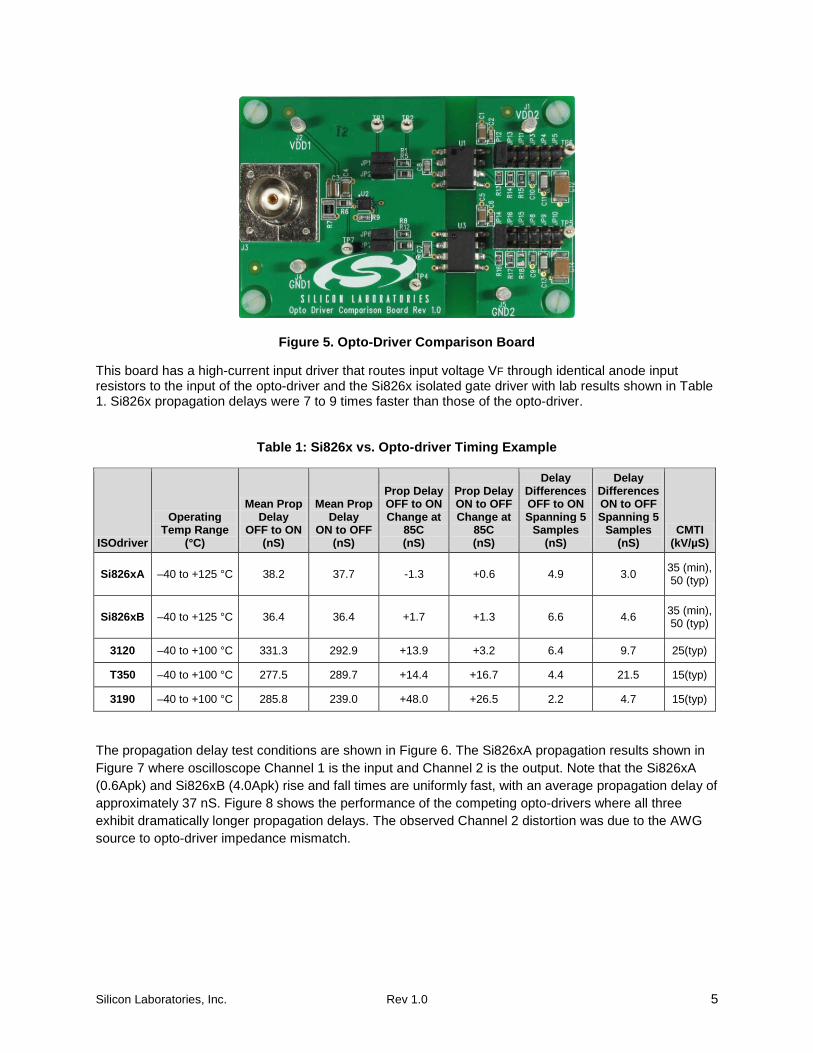
Applications for Si826x Isolated Gate Drivers A side-by-side test between the Silicon Labs’ Si826x opto-driver replacement and the Avago HCPL-3120, ACPL-T350 and ACNW-3190 LED-based gate drive optocouplers, as measured on the Opto-driver Comparison Board of Figure 5.
Silicon Laboratories, Inc. Rev 1.0 5
Figure 5. Opto-Driver Comparison Board
This board has a high-current input driver that routes input voltage VF through identical anode input resistors to the input of the opto-driver and the Si826x isolated gate driver with lab results shown in Table 1. Si826x propagation delays were 7 to 9 times faster than those of the opto-driver.
Table 1: Si826x vs. Opto-driver Timing Example
ISOdriver
Operating Temp Range
(°C)
Mean Prop Delay
OFF to ON (nS)
Mean Prop Delay
ON to OFF (nS)
Prop Delay OFF to ON Change at
85C (nS)
Prop Delay ON to OFF Change at
85C (nS)
Delay Differences OFF to ON Spanning 5
Samples (nS)
Delay Differences ON to OFF Spanning 5
Samples (nS)
CMTI (kV/µS)
Si826xA –40 to +125 °C 38.2 37.7 -1.3 +0.6 4.9 3.0 35 (min), 50 (typ)
Si826xB –40 to +125 °C 36.4 36.4 +1.7 +1.3 6.6 4.6 35 (min), 50 (typ)
3120 –40 to +100 °C 331.3 292.9 +13.9 +3.2 6.4 9.7 25(typ)
T350 –40 to +100 °C 277.5 289.7 +14.4 +16.7 4.4 21.5 15(typ)
3190 –40 to +100 °C 285.8 239.0 +48.0 +26.5 2.2 4.7 15(typ)
The propagation delay test conditions are shown in Figure 6. The Si826xA propagation results shown in Figure 7 where oscilloscope Channel 1 is the input and Channel 2 is the output. Note that the Si826xA (0.6Apk) and Si826xB (4.0Apk) rise and fall times are uniformly fast, with an average propagation delay of approximately 37 nS. Figure 8 shows the performance of the competing opto-drivers where all three exhibit dramatically longer propagation delays. The observed Channel 2 distortion was due to the AWG source to opto-driver impedance mismatch.

Silicon Laboratories, Inc. Rev 1.0 6
DEVICE UNDER TEST
ARBITRARY WAVEFORM GENERATOR
1MHz
IN OUT
24VCH1
CH2
OSCILLOSCOPE
Figure 6. Propagation Delay Measurement Setup
Si826xA Si826xB
Figure 7. Si826xA/B Propagation Delays
Figure 8. Opto-Driver Propagation Delays

Silicon Laboratories, Inc. Rev 1.0 7
A common-mode transient immunity test was performed on all five products to the conditions shown in Figure 9. The results of the Si826x are shown in Figure 10. Figure 11 shows the response of the three opto-drivers. A 670 mV offset was coupled to the output of HCPL-3120, and a 160 mV offset was coupled to the output of the ACNW-3190.
DEVICE UNDER TEST
HV PULSE GENERATOR
1.5kV50nS
IN OUT
5V
SYNC CH2
OSCILLOSCOPE
Figure 9. Propagation Delay Measurement Setup
Figure 10. Si826x Common-Mode Transient Immunity

Silicon Laboratories, Inc. Rev 1.0 8
Figure 11. Opto-Driver Common-Mode Transient Immunity
Summary CMOS-based drop-in gate drive optocoupler replacements offer substantial gains in performance and reliability over traditional opto-drivers. These digital isolation devices are suitable for both new designs and for retrofitting opto-driver sockets without modifications to the PCB, while offering significant increases in performance and reliability with service lifetimes of more than 60 years. Find out more about Silicon Labs’ new Si826x family of digital gate drivers at www.silabs.com/isolation.
# # #
Silicon Labs invests in research and development to help our customers differentiate in the market with innovative low-power, small size, analog intensive, mixed-signal solutions. Silicon Labs' extensive patent portfolio is a testament to our unique approach and world-class engineering team. Patent: www.silabs.com/patent-notice © 2013, Silicon Laboratories Inc. ClockBuilder, DSPLL, Ember, EZMac, EZRadio, EZRadioPRO, EZLink, ISOmodem, Precision32, ProSLIC, QuickSense, Silicon Laboratories and the Silicon Labs logo are trademarks or registered trademarks of Silicon Laboratories Inc. ARM and Cortex-M3 are trademarks or registered trademarks of ARM Holdings. ZigBee is a registered trademark of ZigBee Alliance, Inc. All other product or service names are the property of their respective owners.