pixel-by-pixel local dimming for high- dynamic-range … local dimming for high-dynamic-range liquid...
TRANSCRIPT
Pixel-by-pixel local dimming for high-dynamic-range liquid crystal displays
HAIWEI CHEN,1 RUIDONG ZHU,1 MING-CHUN LI,2 SEOK-LYUL LEE,2 AND
SHIN-TSON WU1,*
1College of Optics and Photonics, University of Central Florida, Orlando, Florida 32816, USA 2AU Optronics Corp., Hsinchu Science Park, Hsinchu 300, Taiwan *[email protected]
Abstract: We propose a high dynamic range (HDR) liquid crystal display (LCD) with pixel-level local dimming. The device structure consists of a pixelated LCD dimming panel to control the backlight intensity entering the master LCD panel. According to our analysis and test cell experiment, this dual-panel display system possesses exceedingly high contrast ratio (> 1,000,000:1) and high bit-depth (> 14 bits) at merely 5 volts. Meanwhile, to mitigate the Moiré effect induced by the cascaded thin-film transistor (TFT) backplanes, we separate the two LCD panels with a polarization-dependent scattering film. The pros and cons of this HDR display are discussed. © 2017 Optical Society of America
OCIS codes: (230.3720) Liquid-crystal devices; (120.2040) Displays; (310.6845) Thin film devices and applications.
References and links
1. H. Seetzen, W. Heidrich, W. Stuerzlinger, G. Ward, L. Whitehead, M. Trentacoste, A. Ghosh, and A. Vorozcovs, “High dynamic range display systems,” ACM Trans. Graph. 23(3), 760–768 (2004).
2. J. U. Kwon, S. Bang, D. Kang, and J. J. Yoo, “The required attribute of displays for high dynamic range,” SID Symp. Dig. Tech. Papers 47(1), 884–887 (2016).
3. S. Daly, T. Kunkel, X. Sun, S. Farrell, and P. Crum, “Viewer preferences for shadow, diffuse, specular, and emissive luminance limits of high dynamic range displays,” SID Symp. Dig. Tech. Papers 44(1), 563–566 (2013).
4. C. H. Oh, H. J. Shin, W. J. Nam, B. C. Ahn, S. Y. Cha, and S. D. Yeo, S.D., “Technological progress and commercialization of OLED TV,” SID Symp. Dig. Tech. Papers 44(1), 239–242 (2013).
5. H. Chen, T. H. Ha, J. H. Sung, H. R. Kim, and B. H. Han, “Evaluation of LCD local-dimming-backlight system,” J. Soc. Inf. Disp. 18(1), 57–65 (2010).
6. F. C. Lin, Y. P. Huang, L. Y. Liao, C. Y. Liao, H. P. D. Shieh, T. M. Wang, and S. C. Yeh, “Dynamic backlight gamma on high dynamic range LCD TVs,” J. Disp. Technol. 4(2), 139–146 (2008).
7. K. Nakajima, H. Tsuchi, Y. Hori, T. Nose, H. Furihata, K. Umeda, and J. Ishii, “A 12-bit LCD source driver IC with point-to-point link interface,” SID Symp. Dig. Tech. Papers 38(1), 1633–1635 (2007).
8. K. J. Kwon, M. B. Kim, C. Heo, S. G. Kim, J. S. Baek, and Y. H. Kim, “Wide color gamut and high dynamic range displays using RGBW LCDs,” Displays 40, 9–16 (2015).
9. D. Lanman, M. Hirsch, Y. Kim, and R. Raskar, “Content-adaptive parallax barriers: optimizing dual-layer 3D displays using low-rank light field factorization,” ACM Trans. Graph. 29(6), 163 (2010).
10. Y. Kitagawa, H. Ikeno, S. Uehara, and T. Yatsushiro, “Dual panel liquid crystal display device,” U.S. Patent 7,916,223 (March 29, 2011).
11. D. Lanman, G. Wetzstein, M. Hirsch, W. Heidrich, and R. Raskar, “Polarization fields: dynamic light field display using multi-layer LCDs,” ACM Trans. Graph. 30(6), 186 (2011).
12. F. C. Huang, K. Chen, and G. Wetzstein, “The light field stereoscope: immersive computer graphics via factored near-eye light field displays with focus cues,” ACM Trans. Graph. 34(4), 60 (2015).
13. M. Schadt and W. Helfrich, “Voltage-dependent optical activity of a twisted nematic liquid crystal,” Appl. Phys. Lett. 18(4), 127–128 (1971).
14. A. Takeda, S. Kataoka, T. Sasaki, H. Chida, H. Tsuda, K. Ohmuro, T. Sasabayashi, Y. Koike, and K. Okamoto, “A super-high image quality multi-domain vertical alignment LCD by new rubbing-less technology,” SID Symp. Dig. Tech. Papers 29(1), 1077–1080 (1998).
15. S. H. Lee, S. L. Lee, and H. Y. Kim, “Electro-optic characteristics and switching principle of a nematic liquid crystal cell controlled by fringe-field switching,” Appl. Phys. Lett. 73(20), 2881–2883 (1998).
16. H. Chen, F. Peng, Z. Luo, D. Xu, S. T. Wu, M. C. Li, S. L. Lee, and W. C. Tsai, “High performance liquid crystal displays with a low dielectric constant material,” Opt. Mater. Express 4(11), 2262–2273 (2014).
17. H. Chen, R. Zhu, J. Zhu, and S. T. Wu, “A simple method to measure the twist elastic constant of a nematic liquid crystal,” Liq. Cryst. 42(12), 1738–1742 (2015).
Vol. 25, No. 3 | 6 Feb 2017 | OPTICS EXPRESS 1973
#282913 http://dx.doi.org/10.1364/OE.25.001973 Journal © 2017 Received 15 Dec 2016; revised 17 Jan 2017; accepted 17 Jan 2017; published 24 Jan 2017

18. A. Chao, K. T. Huang, C. W. Tsai, Y. W. Hung, H. F. Cheng, W. Yeh, C. H. Yu, and H. H. Wu, “The fastest response TN-type TFT LCD of the world likes OCB level,” SID Symp. Dig. Tech. Papers 38(1), 603–606 (2007).
19. H. Chen, Z. Luo, D. Xu, F. Peng, S. T. Wu, M. C. Li, S. L. Lee, and W. C. Tsai, “A fast-response A-film-enhanced fringe field switching liquid crystal display,” Liq. Cryst. 42(4), 537–542 (2015).
20. H. Chen, M. Hu, F. Peng, J. Li, Z. An, and S. T. Wu, “Ultra-low viscosity liquid crystals,” Opt. Mater. Express 5(3), 655–660 (2015).
21. F. Peng, H. Chen, F. Gou, Y. H. Lee, M. Wand, M. C. Li, S. L. Lee, and S. T. Wu, “Analytical equation for the motion picture response time of display devices,” J. Appl. Phys. 121(2), 023108 (2017).
22. H. Chen, F. Peng, F. Gou, Y. H. Lee, M. Wand, and S. T. Wu, “Nematic LCD with motion picture response time comparable to organic LEDs,” Optica 3(9), 1033–1034 (2016).
23. E. Jang, S. Jun, H. Jang, J. Lim, B. Kim, and Y. Kim, “White-light-emitting diodes with quantum dot color converters for display backlights,” Adv. Mater. 22(28), 3076–3080 (2010).
24. R. Zhu, Z. Luo, H. Chen, Y. Dong, and S. T. Wu, “Realizing Rec. 2020 color gamut with quantum dot displays,” Opt. Express 23(18), 23680–23693 (2015).
25. H. Chen, J. He, and S. T. Wu, “Recent Advances on Quantum-Dot-Enhanced Liquid Crystal Displays,” IEEE J. Sel. Top. Quantum Electron. In press (2017).
26. G. Guarnieri, L. Albani, and G. Ramponi, “Minimum-error splitting algorithm for a dual layer LCD display—Part I: Background and theory,” J. Disp. Technol. 4(4), 383–390 (2008).
27. G. Guarnieri, L. Albani, and G. Ramponi, “Minimum-error splitting algorithm for a dual layer LCD display—Part II: Implementation and results,” J. Disp. Technol. 4(4), 391–397 (2008).
28. A. Moheghi, H. Nemati, and D. K. Yang, “Polarizing light waveguide plate from polymer stabilized liquid crystals,” Opt. Mater. Express 5(5), 1217–1223 (2015).
29. A. Moheghi, G. Qin, and D. K. Yang, “Stable polarizing light waveguide plate for edgelit liquid crystal displays,” Opt. Mater. Express 6(2), 429–435 (2016).
1. Introduction
High dynamic range (HDR) is a critical technology for next-generation displays, as it enables the viewer to see supreme image qualities, including higher contrast ratio (CR), darker black state, more gray levels and more vivid colors [1]. To achieve HDR, three basic requirements should be fulfilled: (1) high CR, (2) excellent black state and high peak brightness, and (3) precise control on how and where all these different bright and dark shades be applied to the displayed images [2]. To enlarge CR, both peak brightness and dark state should be improved [3]. For example, the luminance of bright state should be > 1000 nits, while dark state should be < 0.01 nits. In other words, the effective CR is over 100,000:1. For an organic light-emitting diode (OLED) display, it is fairly easy to get true black state, but to obtain a brightness over 1000 nits would lead to compromised lifetime [4]. On the contrary, it is relatively easy to boost an LCD’s peak brightness to 1000 nits, but to lower the dark state to < 0.01 nits is challenging. A typical CR of a multi-domain vertical alignment (MVA) LCD is ~5000:1, which is about 20x lower than what HDR demands. To improve dark state, local dimming technique has been commonly practiced [5, 6].
If a LCD’s CR can be improved by 20x, then more grayscales can be displayed. For a standard dynamic range (SDR) display, 8-bit signal depth is commonly used. However for HDR, at least 10-bit depth is required [2]. The increased bit depth introduces splendid image quality, but may also bring heavier burden to the driving schemes. For thin-film-transistor (TFT) LCDs, the minimal voltage interval between two adjacent gray levels is about 8 mV. Then to achieve 10-bit depth (i.e. 1024 gray levels), the required on-state voltage is 8.19 V. If the signal depth is increased to 12 bits or even 14 bits, then the corresponding on-state voltage is 32.77 V and 131 V, respectively. Such a high operation voltage is beyond what the present TFT can provide. There is an urgent need to increase the bit depth while keeping a low operation voltage [7]. The final requirement of HDR is pixel-level local dimming. For OLED, each pixel is controlled from black state to full bright state easily. But for LCD, the presently employed local dimming is to divide LED backlight into hundreds of segments; it is far from the pixel-level local dimming. With some algorithm optimization, dimming accuracy can be improved [8], but the cost and complexity would also increase. Therefore, how to get HDR LCD with pixel-by-pixel local dimming remains a big challenge.
Vol. 25, No. 3 | 6 Feb 2017 | OPTICS EXPRESS 1974

In this paper, we demonstrate a HDR LCD with two cascaded panels. In fact, dual-layer or even multi-layer LCD has already been widely used in 3D display, volumetric display and light field display [9–12], but few reports are focused on their electro-optical properties. Here, we perform systematic investigations on the dual-panel HDR LCD system, with special emphases on contrast ratio, gray level, operation voltage, response time, viewing angle, and Moiré effect. Our analysis and test cell experimental results indicate that we are able to achieve CR >1,000,000:1 (limited by the noises of our photodiode detector), high bit depth (>14 bits), low operation voltage (~5V), and pixel-level local dimming. To eliminate the Moiré patterns induced by the cascaded TFT backplanes, we introduced a polarization dependent scattering film (PDSF). Potential concerns for the dual-layer system are discussed, such as increased panel thickness, weight, cost, misalignment effect, and reduced optical efficiency. We believe such a HDR LCD would find widespread applications for medical imaging, art designing, movies, and vehicular displays.
2. Design of cascaded LCD panels
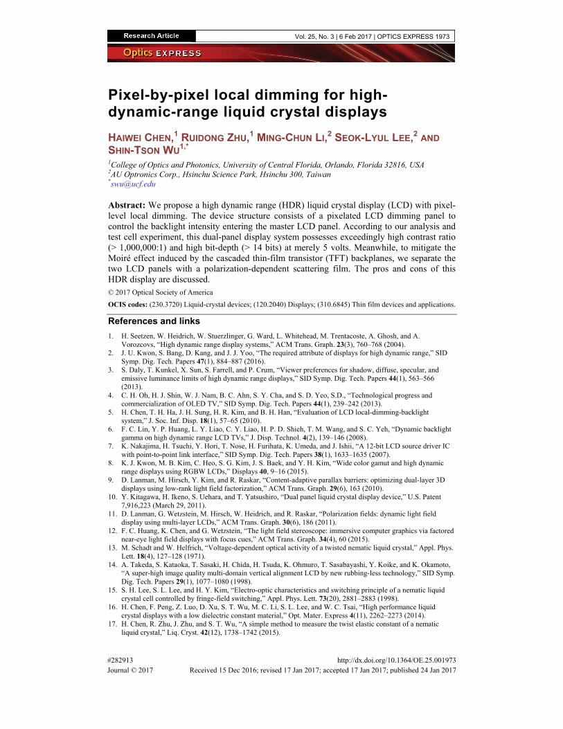
Figure 1 shows the proposed device configuration, consisting of a master display panel (LCD #2) and a pixelated dimming panel (LCD #1). In principle, any two LC modes can be paired up [13–15], e.g. VA and 90° TN (twisted nematic), VA and FFS (fringe-field switching), FFS and TN, two TNs, or two FFSs, just to name a few. However, considering the viewing angle, color shift, and cost, we choose FFS as master display and black-and-white TN (same dimension but without color filters) as local dimmer. TN is a normally-white broadband half-wave plate [14]; that means, at V = 0 the incident white light passes through the TN panel and reaches the master display with high efficiency. If the local dimming is on demand, we can apply different voltages (through TFTs) to those chosen pixels to control their transmittance. While for the FFS panel [15], it shows excellent image quality, including wide viewing angle, unnoticeable color shift, weak gamma shift, and pressure resistance for touch panels. Therefore, we put it in the viewer side. Later, we will use the FFS/TN test cell results to illustrate the operation principles. Let us assume the contrast ratio of the two LCD panels is CR1 and CR2, respectively. Then for the cascaded display system, the effective contrast ratio should be CR1*CR2 [1]. A typical CR for FFS LCD is ~2000:1 and TN is ~800:1, thus ideally the intrinsic CR of dual panels should be 1,600,000:1. Another advantage of this design is pixel-level local dimming, similar to OLED, if two panels are aligned well. Of course, there are some drawbacks, like decreased efficiency, increased cost, and misalignment issue. We will discuss these factors in detail later.
Vol. 25, No. 3 | 6 Feb 2017 | OPTICS EXPRESS 1975
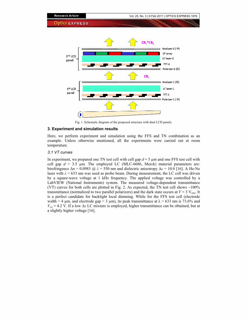
Fig. 1. Schematic diagram of the proposed structure with dual LCD panels.
3. Experiment and simulation results
Here, we perform experiment and simulation using the FFS and TN combination as an example. Unless otherwise mentioned, all the experiments were carried out at room temperature.
3.1 VT curves
In experiment, we prepared one TN test cell with cell gap d = 5 µm and one FFS test cell with cell gap d = 3.5 µm. The employed LC (MLC-6686, Merck) material parameters are: birefringence Δn = 0.0983 @ λ = 550 nm and dielectric anisotropy Δε = 10.0 [16]. A He-Ne laser with λ = 633 nm was used as probe beam. During measurement, the LC cell was driven by a square-wave voltage at 1 kHz frequency. The applied voltage was controlled by a LabVIEW (National Instruments) system. The measured voltage-dependent transmittance (VT) curves for both cells are plotted in Fig. 2. As expected, the TN test cell shows ~100% transmittance (normalized to two parallel polarizers) and the dark state occurs at V = 3 Vrms. It is a perfect candidate for backlight local dimming. While for the FFS test cell (electrode width = 4 µm, and electrode gap = 3 µm), its peak transmittance at λ = 633 nm is 73.6% and Von = 4.2 V. If a low Δε LC mixture is employed, higher transmittance can be obtained, but at a slightly higher voltage [16].
Vol. 25, No. 3 | 6 Feb 2017 | OPTICS EXPRESS 1976

Fig. 2. Measured VT curves for TN and FFS test cells. LC: MLC-6686 with Δε = 10. FFS cell: d = 3.5 µm, electrode width ω = 4 µm, and electrode gap l = 3 µm. λ = 633 nm.
3.2 Contrast ratio
Next, we measured the contrast ratio of these two test cells. Results are CRFFS = 4625:1 and CRTN = 2172:1. When we placed these two cells in sequence (TN is closer to the light source), in principle the CR should reach 9,263,580:1 (CRFFS*CRTN), but in experiment we only obtained CR = 1,102,564:1 when the TN cell was driven at 3 Vrms. This result is 8.4x smaller than the theoretical value, but still much higher than the required 100,000:1 for HDR displays. The reduced CR could be limited by the sensitivity of the photodiode detector we employed. Please note that, here linear polarizers with a high extinction ratio (~18,000:1) were adopted, and the measurement was performed using a He-Ne laser (λ = 633 nm). As a result, the obtained CR would be higher than the traditional value using a white backlight.
3.3 Response time
Figures 3(a) and 3(b) show the measured response time for the FFS cell and TN cell, respectively. Due to the small twist elastic constant [17], FFS cell exhibits a slower response time [rise time: 24.5 ms, decay time: 21.6 ms]; while for TN cell, the measured response time is relatively fast [decay time: 4.4 ms, rise time: 9.7 ms]. Then we combine FFS cell and TN cell together, and investigate the response time of dual-panel system. Results are plotted in Fig. 3(c), where rise time is 19.0 ms, and decay time is 6.4 ms. Interestingly, both rise time and decay time are improved as compared to single FFS cell, especially for decay time (21.6 ms vs. 6.4 ms). It means TN panel helps to accelerate the total transition process effectively. If we use a thinner cell gap with higher Δn yet low viscosity LC, an even faster response time (< 2 ms) can be achieved [18–20]. That way, its motion picture response time would be comparable to that of an OLED display, leading to much suppressed image blurs [21, 22].
Vol. 25, No. 3 | 6 Feb 2017 | OPTICS EXPRESS 1977

Fig. 3. Measured response time for (a) single FFS cell, (b) single TN cell, and (c) combined FFS + TN cell.
3.4 Signal depth
In real applications, two TFT LCD panels are driven independently. That is, TN panel provides pixel-by-pixel dimming, which controls the amount of backlight entering the FFS cell. For example, Fig. 4 shows the transmittance of the FFS/TN combined cell when the TN cell was operated at four different gray levels (25%, 50%, 75% and 100%), while the FFS cell is working normally from dark to bright states continuously.
Fig. 4. Measured VT curves of FFS/TN when the TN cell is at 4 specified transmittance.
Vol. 25, No. 3 | 6 Feb 2017 | OPTICS EXPRESS 1978

As discussed above, the final gray level is jointly determined by both panels. With simple calculations, all the possible gray levels are summarized in Table 1. Deleting the duplicated values, the total number of different gray levels is 17578 by combining two 8-bit LCD panels, which is larger than 14-bit signal depth modulation (214 = 16384). As mentioned above, the required operation voltage for a single-panel LCD with 14-bit grayscales is 131 V. Here, our cascaded LCD panels only requires Von ~5 V to get 14-bit signal depth. The power consumption and design complexity are dramatically reduced.
Table 1. Possible gray levels for two cascaded 8-bit LCD panels.
TN FFS
0 1 2 3 … 253 254 255
0 0 0 0 0 … 0 0 0
1 0 1 2 3 … 253 254 255
2 0 2 4 6 … 506 508 510
3 0 3 6 9 … 759 762 765
… … … … … … … … …
253 0 253 506 759 … 64009 64262 64768
254 0 254 508 762 … 64262 64516 64770
255 0 255 510 765 … 64768 64770 65025
3.5 Viewing angle
Figure 5(a) shows the simulated isocontrast contours for a conventional TN LCD. The highest CR is about 1200:1, and it drops gradually as the viewing cone increases. For some azimuthal angle, say 230°, it is less than 10:1, which means the image quality is degraded greatly. For FFS LCD [Fig. 5(b)], its CR could reach ~2500:1, but still drop to 100:1 at large viewing angles.
Fig. 5. Calculated isocontrast contour for (a) single TN panel and (b) single FFS panel.
When we cascade them together, the CR exceeds 1,000,000:1 within the ~20° viewing cone, as shown in Fig. 6. Even for the entire viewing zone, CR still keeps over 1000:1. If we define the HDR requirement as 100,000:1, then the viewing angle in the horizontal direction is extended to about 60°. Meanwhile, since we use FFS as master display panel, its color shift
Vol. 25, No. 3 | 6 Feb 2017 | OPTICS EXPRESS 1979

and gamma shift are very weak. If we combine with quantum dot backlight, then the color gamut of ~90% Rec.2020 can be obtained [23–25].
Fig. 6. Simulated isocontrast contour for the cascaded FFS and TN panels.
4. Potential concerns
As above mentioned, dual LCD panels show great advantages in contrast ratio, signal depth and viewing angle. However, some challenges remain to be solved. The first one is increased cost, because two panels are used. Fortunately, the portion of panel cost to the total price is not high. For example, in a 5” FHD smartphone, the LCD panel is only $15. Compared to the total price $500 of a smartphone, the display part only occupies ~3%. For large size TVs, this portion increases, but is still acceptable. On the other hand, cost is less a concern for some high-end devices, like medical diagnosis, movie directing, photographers, universe detecting, art designers, etc.
Increased thickness is another potential concern for the dual LCD panels. For a conventional edge-lit LCD, the panel thickness is about 1.6 mm. And for direct-lit backlight with local dimming, the total thickness is ~5 mm. As shown in Fig. 1, in our design, one more LC panel is added, consisting of two polarizers (130 µm * 2), two substrates (200 µm * 2), LC layer (4 µm), and compensation films (150 µm). The increased thickness is ~0.9 mm. Therefore, for the whole device it is 2.5-mm thick, which is still ~2x thinner than the direct-lit display.
The other issue for dual LCD panels is decreased efficiency, which mainly results from the additional polarizers. Because of the absorption of polarizer, in our experiment, the optical efficiency of dual-panel system (i.e. FFS + TN) is reduced by 25% (surface reflection is considered), as compared to that of a single panel (i.e. FFS). Also, the electrical power consumption will also increase as two panels need to be driven independently.
Next issue is misalignment. If two LC panels don’t align precisely, then the image would be distorted. Fortunately, this issue could be mitigated from image processing part. Guarnieri et al. developed a novel splitting algorithm to minimize the errors caused by misalignment [26, 27]. Based on their analysis, the images could still remain in good quality even though there is 3-pixel spatial shift between two LCD panels.
5. Moiré effect
When two LCD panels are laminated together, Moiré effect appears because of the patterned TFT backplanes. To reduce this effect, a strong diffuser is often employed. But if we use such
Vol. 25, No. 3 | 6 Feb 2017 | OPTICS EXPRESS 1980

a diffuser, the output light from the dimming panel will be depolarized and the overall performance degraded significantly. To overcome this problem, here we propose to use a new polarization dependent scattering film (PDSF) [28, 29], as depicted in Fig. 7. The system configuration is quite similar to that shown in Fig. 1; the only difference is that the analyzer in the dimming panel is replaced by a PDSF. This PSDF exhibits a unique property: polarization dependent scattering. For example, PSDF would scatter the s-wave strongly, while transmitting the p-wave. With this unique scattering property, Moiré effect is mitigated while keeping a high CR for the dual LCD panels.
Fig. 7. Schematic diagram for the proposed structure using a PDSF to replace Analyzer-1.
To fabricate PSDF, in experiment we prepared a LC/monomer mixture consisting of BL038 (95.6 wt%), RM257 (4.2 wt%) and Irg651 (0.2 wt%). A homogeneous cell with cell gap d = 12 µm was employed. The LC test cell was first cured using a UV lamp (λ ≈365 nm and intensity 5 mW/cm2) for 30 s. After that we applied 20 V to the cell and cured it again for 1 hour with the same UV intensity. Then a multi-domain structure is obtained, as shown in Fig. 8(a). When the incident light is linearly polarized along x-axis [Fig. 8(b)], it gets scattered due to the non-uniform refractive indices in PDSF. Whereas for y-polarized incident light [Fig. 8(c)], the corresponding refractive index is uniform, i.e. no, therefore, it could traverse through PDSF without scattering.
Vol. 25, No. 3 | 6 Feb 2017 | OPTICS EXPRESS 1981

Fig. 8. (a) Schematic diagrams for the PDSF fabrications. Step 1: homogeneous state before polymerization; Step 2: polymerization without applied voltage; Step 3: polymerization with applied voltage. (b) Scattering state for x-polarized incident light. (c) Transmission state for y-polarized incident light.
Fig. 9. Experimental setup for characterizing PDSF.
The measurement setup is depicted in Fig. 9, where a He-Ne laser was used as probing beam and the acceptance angle of the photodiode detector was 4.5°. When we rotate the PDSF, the incident polarization changes, as a result, the transmitted light intensity after PDSF changes accordingly. Figure 10 depicts the measured result. The peak transmittance for the p-wave is 75%, while in the scattering state (s-wave) the transmittance drops to 2.6%. The measured CR is about 28.6:1.
Vol. 25, No. 3 | 6 Feb 2017 | OPTICS EXPRESS 1982

0 20 40 60 80 100 120 140 160 1800.0
0.1
0.2
0.3
0.4
0.5
0.6
0.7
0.8
Tra
nsm
itta
nce
Angle (o)
Fig. 10. Measured transmittance of PSDF at different polarization angles. λ = 633nm.
In another experiment, we measured the transmittance and scattering spectra of PDSF with a linearly polarized white light. Results are plotted in Fig. 11. As the wavelength decreases, the scattering gets stronger, leading to a decreased transmittance. Please note that even at clear state, the transmittance is still much lower than 100%. That means there is ~25% of the incident backlight is scattered. Such a light diffuser helps to suppress the Moiré effect, although the total optical efficiency is reduced. For practical applications, the transmittance and scattering properties of PSDF need to be optimized in order to eliminate the Moiré effect.
400 450 500 550 600 650 7000.0
0.2
0.4
0.6
0.8
1.0
Inte
nsi
ty
Wavelength (nm)
Transmittance Scattering
Fig. 11. Measured transmission and scattering spectra of the PDSF.
Next, we incorporate this PDSF with a TN cell to constitute the first LCD panel, and the obtained VT curve is plotted in Fig. 12. Clearly, the outgoing light intensity (backlight entering the master LCD panel) can be controlled pixel-by-pixel through the TN LCD. The required voltage is ≤ 3V. When incorporating with our FFS cell, the measured CR is ~116,000:1, which is slightly higher than the desired value (> 100,000:1) for HDR displays. To further improve the overall CR, PDSF should be further optimized, including its recipe, curing condition, and film thickness. Another option to boost the CR is to add the displaced Analyzer-1 back to the first LCD panel. That is, the PDSF film is positioned between Analyzer-1 and Polarizer-2, as Fig. 1 depicts. Under such a condition, an exceedingly high
Vol. 25, No. 3 | 6 Feb 2017 | OPTICS EXPRESS 1983

CR can be restored, but the tradeoffs are increased panel thickness and ~15% lower light efficiency.
Fig. 12. Measured VT curve for PDSF with a TN cell.
6. Conclusion
We proposed a HDR display with two cascaded LCD panels and proved the design concept by using a FFS and a TN LC cells. The device performance is quite promising, including high contrast ratio (> 1,000,000:1), high bit depth (> 14 bits), and pixel-level local dimming. But some technical challenges remain to be addressed, such as pixel misalignment, decreased optical efficiency, increased panel thickness and power consumption. Also, Morié effect is a big problem, which degrades the image quality. To mitigate that, we added a polarization dependent scattering film between two LCD panels. Such a HDR display would find new applications for medical imaging, movies, and vehicular displays.
Funding
AFOSR (FA9550-14-1-0279)
Acknowledgments
The authors would like to thank Fenglin Peng and Guanjun Tan for helpful discussion, and a.u.Vista, Inc. for partial financial support.
Vol. 25, No. 3 | 6 Feb 2017 | OPTICS EXPRESS 1984