placement of thermal vias in 3d ics using various thermal ...localized hot spots directly. despite...
TRANSCRIPT

Placement of Thermal Vias in 3D ICs using Various Thermal Objectives
Brent Goplen, Sachin S. Sapatnekar
Department of Electrical and Computer Engineering
University of Minnesota
200 Union ST SE, Minneapolis, MN 55455
{bgoplen, sachin}@ece.umn.edu
ABSTRACT
As thermal problems become more evident, new physical design paradigms and tools are needed to alleviate
them. Incorporating thermal vias into integrated circuits (ICs) is a promising way of mitigating thermal issues by
lowering the effective thermal resistance of the chip. However, thermal vias take up valuable routing space, and
therefore, algorithms are needed to minimize their usage while placing them in areas where they would make the
greatest impact. With the developing technology of three-dimensional integrated circuits (3D ICs), thermal
problems are expected to be more prominent, and thermal vias can have a larger impact on them than in
traditional 2D ICs. In this paper, thermal vias are assigned to specific areas of a 3D IC and used to adjust their
effective thermal conductivities. The method, which uses finite element analysis (FEA) to calculate temperatures
quickly during each iteration, makes iterative adjustments to these thermal conductivities in order to achieve a
desired thermal objective and is general enough to handle a number of different thermal objectives such as
achieving a desired maximum operating temperature. With this method, 49% fewer thermal vias are needed to
obtain a 47% reduction in the maximum temperatures, and 57% fewer thermal vias are needed to obtain a 68%
reduction in the maximum thermal gradients than would be needed using a uniform distribution of thermal vias to
obtain these same thermal improvements. Similar results were seen for other thermal objectives, and the method
efficiently achieves its thermal objective while minimizing the thermal via utilization.
This work was supported in part by an SRC fellowship and by DARPA under grant N66001-04-1-8909.

2
Categories and Subject Descriptors
B.7.2 [Integrated Circuits]: Design Aids – Placement and routing; B.7.1 [Integrated Circuits]: Types and
Design Styles – Advanced technologies
General Terms
Algorithms, Performance, Design, Experimentation
Keywords
3-D IC, 3-D VLSI, thermal optimization, temperature, thermal gradient, placement, routing, finite element
analysis, thermal via
1. INTRODUCTION
As the technology node progresses, chip areas and wire lengths continue to increase, causing such problems
as increased interconnect delays, power consumption, and temperature, all of which can have serious
implications on reliability, performance, and design effort. Three dimensional technology attempts to overcome
some of these limitations by stacking multiple active layers into a monolithic structure, using special processing
technologies such as silicon-on-insulator (SOI) or wafer bonding [1]. By expanding vertically rather than
spreading out over a larger area, the chip space is better utilized, interconnects are decreased, and transistor
packing densities are increased, leading to better performance and power efficiency [2]. Despite the advantages
that 3D ICs have over 2D ICs, thermal effects are expected to be more pronounced because of higher power
densities and greater thermal resistance along heat dissipation paths. With the advent of better processing
technologies for 3D ICs, design tools are needed to realize their full potential and overcome thermal and
efficiency issues. Current design tools used for 2D ICs can not be easily extended to 3D ICs [2], especially when
taking into account thermal effects.
The idea of using thermal vias to alleviate thermal problems was first utilized in the design of packaging and

3
printed circuit boards (PCBs). Lee et al. studied arrangements of thermal vias in the packaging of multichip
modules (MCMs) and found that as the size of thermal via islands increased, more heat removal was achieved but
less space was available for routing [3]. Li studied the relationships between design parameters and the thermal
resistance of thermal via clusters in PCBs and packaging [4]. These relationships were determined by
simplifying the via cluster into parallel networks using the observation that heat transfer is much more efficient
vertically through the thickness than laterally from heat spreading. Pinjala et al. performed further thermal
characterizations of thermal vias in packaging [5]. Although these papers have limited application for the
placement of thermal vias inside chips, the basic use and properties of thermal via are demonstrated. It is
important to realize that there is a tradeoff between routing space and heat removal, indicating that thermal vias
should be used sparingly. Simplified thermal calculations can be used for thermal vias, and the direction of heat
conduction is primarily in the orientation of the thermal via.
Chiang et al. first suggested that “dummy thermal vias” can be added to the chip substrate as additional
electrically isolated vias to reduce effective thermal resistances and potential thermal problems [6]. A number of
papers have addressed the potential of integrating thermal vias directly inside chips to reduce thermal problems
internally [6,7,8,9]. Because of the insulating effects of numerous dielectric layers, thermal problems are greater
and thermal vias can have a larger impact in 3D ICs than 2D ICs. In addition, interconnect structures can create
efficient thermal conduits and greatly reduce chip temperatures.
It has become of particular interest to design efficient heat conduction paths right into a chip to eliminate
localized hot spots directly. Despite all the work that has been done in evaluating thermal vias, thermal via
placement algorithms are lacking for both 3D and 2D ICs. As circuits and temperature profiles increase in
complexity, efficient algorithms are needed to accurately determine the location and number of internal thermal
vias. The thermal via placement method [10] presented in this paper uses designated thermal via regions to place
thermal vias and efficiently adjusts the density of thermal vias in each of these regions with minimal
perturbations on routing. In the design process, thermal via placement can be applied after placement and before
routing.

4
2. THERMAL VIA REGIONS
Figure 1. Uniform density of thermal vias within a region.
In order to make the placement of thermal vias more manageable, certain areas of the chip are reserved for
placing thermal vias. In a thermal via region as shown in Figure 1, a uniform density of thermal vias is used, and
the thermal via placement algorithm determines the density in each of these regions. In a 3D IC as shown in
Figure 2, these regions are evenly placed between the rows in a standard cell design.
Figure 2. Thermal mesh for a 3D IC, with thermal via regions.
The thermal via regions are composed of electrically isolated vias and are oriented vertically between the
rows. The density of the thermal vias determines the thermal conductivity of the region which in turn determines
the thermal properties of the entire chip. They are generally obstacles to routing except for regions that require
only a low density of thermal vias. Placing thermal vias in specific regions allows for predictable obstacles to
routing, and allows for regularity and uniformity in the entire design process. Moreover, the density of these
y
z
x
Thermal Via Region
Row Region
Inter-Row Region
} Inter-layer
} Layer
z
x
Bulk Substrate
Substrate
Thermal Via

5
routing obstacles is limited in any particular area so that the design does not become unroutable.
The value of the thermal conductivity, K, in any particular direction corresponds to the density of thermal
vias that are arranged in that direction. Increasing the number of thermal vias in one direction does increase the
thermal conductivity in the other directions but at an order of magnitude less. For simplicity, the
interdependence can be considered to be negligible, and the K’s in the x, y, and z directions can be considered to
be independent to a certain extent.
Current integration technologies for producing 3D ICs result in the layers being closely stacked together and
the design space being tightly compressed in the z direction. In addition, the location of the heat sink in relation
to the heat sources produces a heat flux that is primarily downward in direction with very minor lateral
components. Furthermore, with the thermal via regions being oriented vertically, lateral thermal vias would have
little effect. As a result, lateral thermal conductivities (in the x and y directions) are generally unchanged by this
method because the thermal gradients in the vertical (z) direction are almost two orders of magnitude larger than
in the lateral directions. In this paper, the method will be developed for all three directions, but for the reasons
outlined above, only vertically oriented thermal vias will be considered in the implementation and results.
3. TEMPERATURE CALCULATION
At steady state, heat conduction within the chip substrate can be described by the following differential
equation:
( ) 02
2
2
2
2
2
=+∂∂+
∂∂+
∂∂
x,y,zQz
TK
y
TK
x
TK zyx (1)
where T is the temperature, Kx, Ky, and Kz are the thermal conductivities, and Q is the heat generated per unit
volume. A unique solution exists when convective, isothermal, and/or insulating boundary conditions are
appropriately applied. The nature of the packaging and heat sink determines the boundary conditions. The FEA
method from [11] was used for temperature calculations in these experiments. An overview of this method, as
applied to 3D ICs, is presented in the remainder of this section.

6
3.1. FEA Background
In finite element analysis, the design space is first discretized or meshed into elements. An example of an 8-
node hexahedral element is shown in Figure 3. The temperatures are calculated at discrete points (the nodes of
the element), and the temperatures elsewhere within the element are interpolated using a weighted average of the
temperatures at the nodes.
Figure 3. An 8-node hexahedral element.
For an 8-node hexahedral (rectangular prism) element, the following interpolation function is used:
( ) [ ]{ } ∑=
==8
1iiitN tNx,y,zT (2)
where [N ]=[N1 N2 … N8 ], { t}={ t1 t2 … t8}T, ti is the temperature at node i, and Ni is the shape function for
node i. The shape functions are determined by the coordinates of the element’s center, (xc, yc, zc), the coordinates
at the nodes, (xi, yi, zi), the width, w, height, h, and depth, d, of the element.
( ) ( ) ( ) ( ) ( ) ( )
−−
+
−−
+
−−
+= cci
cci
cci
i zzd
zzyy
h
yyxx
w
xxN
222
2
2
12
2
12
2
1 (3)
From the shape functions, the thermal gradient, {g}, can be found as follows:
{ } [ ]{ }tBz
T
y
T
x
Tg =
∂∂
∂∂
∂∂=
T
[ ]
∂∂
∂∂
∂∂
∂∂
∂∂
∂∂
∂∂
∂∂
∂∂
=
z
N
z
N
z
Ny
N
y
N
y
Nx
N
x
N
x
N
B
821
821
821
where
L
L
L
. (4)
z
y
x
1
3 4
2
w
h d
6
8
5

7
Similar to circuit simulation using the modified nodal formulation, stamps are created for each element and
added to the global system of equations. In FEA, these stamps are called element stiffness matrices, [kc], and can
be derived as follows using the variational method for an arbitrary element type [12]:
[ ] [ ] [ ][ ]∫∫∫=V
c dVBDBk T (5)
[ ]
=
z
y
x
K
K
K
D
00
00
00
where and Kx, Ky, and Kz are, respectively, the thermal conductivities in the x, y, and z
directions.
3.2. Application of FEA
For a right prism with a width of w, a height of h, and a depth of d as shown in Figure 3, the element stiffness
matrix is given in Equation (6) as an 8x8 symmetrical matrix with rows and columns corresponding to the nodes
1 through 8 [11].
[ ]
++++++++++++++++++++++++++++++++++++++++++++++++++++++++++++++++
=
ABCDEFGH
BADCFEHG
CDABGHEF
DCBAHGFE
EFGHABCD
FEHGBADC
GHEFCDAB
HGFEDCBA
kc (6)
d
whK
h
wdK
w
hdKH
d
whK
h
wdK
w
hdKG
d
whK
h
wdK
w
hdKF
d
whK
h
wdK
w
hdK
d
whK
h
wdK
w
hdKD
d
whK
h
wdK
w
hdKC
d
whK
h
wdK
w
hdKB
d
whK
h
wdK
w
hdKA
zyxzyx
zyxzyx
zyxzyx
zyxzyx
181836 ,
363636
183618 ,
91818 E
18918 ,
361818
18189 ,
999 where
−−=−−−=
−+−=−+=
+−=+−−=
++−=++=
For the entire mesh, the elements are aligned in a grid pattern with nodes being shared among at most 8
8
different elements. The element stiffness matrices are combined into a global stiffness matrix, [Kglobal], by adding
the components of the element matrices corresponding to the same node together. The global heat vector, {P},
contains power dissipated or heat generation as represented at the nodes. This is produced by distributing the
heat generated by the standard cells among its closest nodes. A linear system of equations is produced,
[K global]{T} = {P} with {T} being a vector of all the nodal temperatures.
3.3. Isothermic Boundary Conditions
Isothermic boundary conditions are applied to the global matrix using the following procedure [12], and this
results in a reduced, nonsingular system of equations. Rows and columns that correspond to fixed temperature
values within the global matrix are eliminated, as are the corresponding values in the power vector, and the
remaining values in the right-hand side vector are modified using the fixed temperature values. For example,
consider the following system:
=
2
1
2
1
2221
1211
P
P
T
T
AA
AA (7)
Here, A11, A12, A21, and A22 represent arrays of elements in the global stiffness matrix, T1 is the vector of
unknown temperatures, T2 is the vector of fixed temperatures, P1 is the vector of the known power values
corresponding to the unknown values, T1, and P2 is the vector of the unknown power values corresponding to the
known values, T2. This system can be reduced as follows:
[ ]{ } { } [ ]{ }2121111 TAPTA −= (8)
A11 is a nonsingular matrix, T1 contain the unknowns, and the right-hand side is vector of constants so this linear
system of equations can now be solved.
3.4. Meshing the 3D IC
In this method, 3D ICs are meshed into regions (elements) as shown in Figure 2. Vertically (in the z
direction), the chip is separated into bulk substrate, layer, and inter-layer elements. The bulk substrate is located

9
at the bottom attached to the heat sink. Above the bulk substrate elements are the layer and inter-layer elements.
In a 3D IC, the inter-layers are composed of inter-layer vias and bonding materials that connect the layers
together, and the layers contain the device and metal levels. Transistors, the primary sources of heat, are located
at the bottom of each layer in the row regions. In standard cell designs, cells are placed into rows with inter-row
spaces between them. These inter-row regions are necessary to accommodate interconnects between different
layers, and some of these areas can serve as thermal via regions. In our method, thermal via regions are
represented as special elements having variable thermal conductivities in the FEA mesh.
4. ITERATIVE THERMAL VIA METHOD
For a given placed 3D circuit, an iterative method was developed in which, during each iteration, the thermal
conductivities of certain FEA elements (thermal via regions) are incrementally modified so that thermal problems
are reduced or eliminated. Thermal vias are generically added to elements to achieve the desired thermal
conductivities. The goal of this method is to satisfy given thermal requirements using as few thermal vias as
possible, i.e., keeping the thermal conductivities as low as possible.
4.1. Updating the Thermal Conductivities
During each iteration, the thermal conductivities of thermal via regions are modified, and these thermal
conductivities reflect the density of thermal vias needed to be utilized within the region. The new thermal
conductivities are derived from the element FEA equations. Using Equation (6), we get:
[ ]{ } { }ptkc = (9)
where {t} are the nodal temperatures in the element and {p} are the fractions of the nodal heat that transverse this
particular element. Under the reasonable assumption that {p} does not change between the old and new values in
an iteration, we get the following expression:
[ ] { } [ ] { }oldoldcnewnewc tktk = (10)
If we multiply Equation (10) by [ ]111111112
−−−−hd
w , [ ]111111112
−−−−wd
h , and

10
[ ]111111112
−−−−wh
d , respectively, we obtain the following equations:
oldx
oldx
newx
newx tKtK ∆=∆ (11)
oldy
oldy
newx
newy tKtK ∆=∆ (12)
oldz
oldz
newz
newz tKtK ∆=∆ (13)
.44
and ,44
44 ,
44
44 ,
44 where
7654321076543210
7632541076325410
6521743065217430
oldoldoldoldoldoldoldoldoldz
newnewnewnewnewnewnewnewnewz
oldoldoldoldoldoldoldoldoldy
newnewnewnewnewnewnewnewnewy
oldoldoldoldoldoldoldoldoldx
newnewnewnewnewnewnewnewnewx
ttttttttt
ttttttttt
ttttttttt
ttttttttt
ttttttttt
ttttttttt
+++−
+++=∆
+++−
+++=∆
+++−
+++=∆
+++−
+++=∆
+++−
+++=∆
+++−
+++=∆
oldz
oldy
oldx KKK and , , are the thermal conductivities in the x, y, and z directions before the iteration.
newz
newy
newx KKK and , , are the thermal conductivities in the x, y, and z directions after the iteration.
oldz
oldy
oldx ttt ∆∆∆ and , , are the change in temperature across the element with respect to the x, y, and z directions
before the iteration. newz
newy
newx ttt ∆∆∆ and , , are the change in temperature across the element with respect to the
x, y, and z directions after the iteration.
The thermal gradients, gnew = {gxnew, gy
new, gznew} and gold = {gx
old, gyold, gz
old}, are functions of the position, (x,
y, z), in the element, and at the center of the element, (xc, yc, zc), they are equal to:
w
tg
w
tg
oldxold
x
newxnew
x
∆=
∆= , (14, 15)
h
tg
h
tg
oldyold
y
newynew
y
∆=
∆= , (16, 17)
d
tg
d
tg
oldzold
z
newznew
z
∆=
∆= , (18, 19)
gnew is the desired new thermal gradient, and gold is the thermal gradient of the element before the iteration. The
new K’s can be found by combining Equations (11)-(19):

11
newx
oldx
oldx
newx
oldx
oldxnew
xg
gK
t
tKK =
∆∆
= (20)
newx
oldy
oldy
newx
oldy
oldynew
yg
gK
t
tKK =
∆
∆= (21)
newz
oldz
oldz
newz
oldz
oldznew
zg
gK
t
tKK =
∆∆
= (22)
{ gxnew, gy
new, gznew} is chosen so that its component magnitudes are closer to some ideal thermal gradient value,
gideal, than {gxold, gy
old, gzold} using the following equations:
α
=
ideal
oldx
idealnewx g
ggg (23)
α
=
ideal
oldy
idealnewy g
ggg (24)
α
=
ideal
oldz
idealnewz g
ggg (25)
where gideal is a nonnegative value and α is a user defined parameter between 0 and 1. If the magnitude of the old
thermal gradient is below gideal, the value is increased toward gideal for the new thermal gradient. If the magnitude
of the old thermal gradient is above gideal, the value is decreased toward gideal. If the magnitude of the old thermal
gradient equals gideal, then the thermal gradient is not modified.
Combining Equations (20)-(25) yields the following formulas that can be used to update the thermal
conductivities during each iteration:
α−
=
1
ideal
oldxold
xnewx g
gKK (26)

12
α−
=
1
ideal
oldyold
ynewy g
gKK (27)
α−
=
1
ideal
oldzold
znewz g
gKK (28)
These formulas decrease the K’s when the thermal gradient is below gideal and increase them when the thermal
gradient is above gideal. In the process, major sources of thermal impedance are eliminated in areas of greatest
heat transfer, but for areas that are not on a critical heat sinking path, the K’s are decreased to eliminate
unnecessary thermal vias.
The ideal thermal gradients, gideal, must be chosen and specifically adjusted to satisfy some desired thermal
objective. This method is flexible enough to handle a number of different thermal objectives, but only one
thermal objective can be used at a time. Each objective type produces a different version of the thermal via
placement method to specifically reach its objective value. For example, six different objective types were
explored in these experiments: maximum thermal gradient, average thermal gradient, maximum temperature,
average temperature, maximum thermal via density, and average thermal via density. Before the first iteration,
the ideal thermal gradient is initialized to the magnitude of the average thermal gradient. Each objective type
uses a different equation to update the ideal thermal gradient during each iteration, and they are listed as follows:
max
idealmax
idealideal g
ggg = for an ideal maximum thermal gradient, ideal
maxg (29)
ave
idealave
idealideal g
ggg = for an ideal average thermal gradient, ideal
aveg (30)
max
idealmax
idealideal T
Tgg = for an ideal maximum temperature, ideal
maxT (31)
ave
idealave
idealideal T
Tgg = for an ideal average temperature, ideal
aveT (32)

13
idealmax
maxidealideal
m
mgg = for an ideal maximum thermal via density, ideal
maxm (33)
idealave
aveidealideal
m
mgg = for an ideal average thermal via density, ideal
avem (34)
For the thermal gradient and temperature objective types, if the value is too low in the previous iteration, gideal
is increased for Equations (29)-(32). Likewise, if the previous value exceeds the desired value, gideal is decreased
to lower the thermal effects. For the thermal via density objective types in Equations (33) and (34), if the
previous iteration’s value is too low, gideal is decreased so more thermal vias will be needed. If the previous
iteration’s value is too high, gideal is increased so fewer thermal vias will be used. Other thermal objectives are
possible with this method as long as an appropriate equation is used to update the ideal thermal gradient and the
value of the objective is reachable.
4.2. Thermal Via Density
As stated earlier, the thermal conductivity of a thermal via region is determined by its density of thermal vias.
After thermal via placement determines the required thermal conductivities, the thermal via densities can be
determined. Individual thermal vias are assumed to be much smaller than the thermal via region, are arranged
uniformly within the thermal via region, and change the effective thermal conductivity of the thermal via region.
The percentage of thermal vias or metalization, m, (also called thermal via density) in a thermal via region is
given by the following equation:
wh
nAm via= (35)
where n is the number of individual thermal vias in the region, Avia is the cross sectional area of each thermal via,
w is the width of the region, and h is the height of the region. The relationship between the percentage of thermal
vias and the effective vertical thermal conductivity is given by:
( ) layerzvia
effz KmmKK −+= 1 (36)
where Kvia is the thermal conductivity of the via material and Kzlayer is the thermal conductivity of the region

14
without any thermal vias. Using this equation, the percentage of thermal vias can be found for any Kznew provided
that Kzlayer ≤ Kz
new ≤ Kvia:
layerzvia
layerz
newz
KK
KKm
−−= (37)
In this implementation, only the vertical thermal conductivities will be optimized using Equation (28).
Equations (26) and (27) will not be used for updating the lateral thermal conductivities because the thermal vias
are only oriented vertically in these experiments. During each iteration, the new vertical thermal conductivity is
used to calculate the thermal via density, m, and the lateral thermal conductivities for each thermal via region.
The effective lateral thermal conductivity can be found using the percentage of thermal vias, m:
( )via
layerlateral
layerlateral
effy
effx
K
m
K
m
mKmKK
+−+−==
11 (38)
Table 1. Thermal Conductivities of Thermal Vias Regions
Layer Interlayer Chip Average Thermal
Conductivity (W·m-1
·K-1)
Thermal Conductivity (W·m-1
·K-1)
Thermal Conductivity (W·m-1
·K-1)
Vertical Lateral
Percent Thermal
Via Vertical Lateral
Percent Thermal
Via Vertical Lateral
Percent Thermal
Via
Minimum 1.11 2.15 0% 1.10 1.10 0% 1.11 2.06 0% Midrange 100.33 3.21 25% 50.71 1.31 12.5% 96.13 3.05 23.9% Maximum 199.55 5.75 50% 100.33 1.65 25% 191.14 5.40 47.9%
Figure 4 and Table 1 show the relationship between the thermal vias densities and the thermal conductivities
in the vertical and lateral directions for thermal via regions having vertically oriented thermal vias. In Figure 4,
Equations (36) and (38) were used to plot the relationship between the percentage of thermal vias in a thermal via
region and its effective thermal conductivities (in units of W·m-1·K-1). It can be seen that the vertically oriented
vias (as shown in Figure 1) produce a much greater effect in the vertical thermal conductivity. In Table 1, the
minimum, midrange, and maximum thermal conductivity values are given. In the midrange case, the average of
the minimum and the maximum thermal via density values of each thermal via region was used.

15
The Relationship between Thermal Via Density and Thermal Conductivity
0
1
2
3
4
5
6
0% 5% 10% 15% 20% 25% 30% 35% 40% 45% 50%
Percent Metallization
Late
ral t
herm
al c
ondu
ctiv
ity
0
50
100
150
200
250
300
Ver
tical
the
rmal
con
duct
ivity
Figure 4. Percentage of thermal vias vs. thermal conductivity.
5. IMPLEMENTATION
THERMAL_VIA_PLACEMENT(objective) { SET gideal TO gave SET K’s TO MININUM CALCULATE TEMPERATURE PROFILE WHILE NOT CONVERGED {
FOR EACH THERMAL VIA REGION { Kz = Kz (| gz|/ gideal)
1- α UPDATE Klateral
} CALCULATE TEMPERATURE PROFILE UPDATE gideal USING objective
} }
Figure 5. Pseudocode of the thermal via placement algorithm.
In the thermal via placement method shown in Figure 5, the thermal gradients are used to update the thermal
conductivities of the thermal via regions. In the process, the thermal gradients are compared to an ideal thermal
gradient value which is modified during each iteration so that a certain objective is reached. In our
implementation, the desired objective value for one of six different objective types is used by the algorithm:
maximum thermal gradient, average thermal gradient, maximum temperature, average temperature, maximum

16
thermal via density, or average thermal via density. Based on the objective type, the ideal thermal gradient is
updated accordingly during each iteration.
The thermal via placement algorithm is initialized by setting the ideal thermal gradient, gideal, to the average
thermal gradient, gave, obtained in the midrange case. In addition, all thermal conductivities (K’s) are set to their
minimum values, and an initial temperature profile is calculated before entering the main loop. Temperature
profiles are calculated using FEA, as described in Section 3, and this gives the temperatures of the nodes and
thermal gradients of the elements.
In each iteration of the main loop, the thermal conductivities of the thermal via regions are modified, and the
temperature profile of the chip is recalculated using the new thermal conductivities. For each thermal via region,
the vertical thermal gradient, gz, at the center of the element is calculated using Equation (19). Using the
magnitude of gz, a new vertical thermal conductivity, Kz, is calculated using Equation (28) (α is set to 0.5 in these
experiments). If the new thermal conductivity exceeds the minimum or maximum value for that element, it is
modified to the value of the bound that it exceeds. Using the new vertical thermal conductivity, the thermal via
density and lateral thermal conductivities, Klateral, are also updated using Equations (37) and (38).
Using the new temperature profile of the chip, the ideal thermal gradient is modifying with the desired
objective value using Equation (29), (30), (31), (32), (33), or (34) depending on which objective type is used.
The algorithm terminates after the 1-norm of the change in the K’s is less than some small ε > 0 and percent
difference between the current value and desired objective value is also within ε.
In choosing a desired objective value to be given to the algorithm, it must be between the values obtained
when all the K’s are minimized and all the K’s are maximized. The algorithm simply finds the configuration of
thermal vias between these two extremes that gives the desired objective value. For example, if an ideal
maximum temperature,idealmaxT , for the chip is desired, it must be less than the maximum temperature obtained
when all the K’s are minimized and greater than the maximum temperature obtained when all the K’s are
maximized in order for this maximum temperature to be realizable. In these experiments, the desired objective

17
values were used from the case where all the thermal via regions were given the midrange values as shown in
Table 1. This gives thermal gradient and temperature values that are greatly reduced from the case when no
thermal vias were used and provides a comparison to the case where all the thermal via regions are given the
same via density. In practice, it would be useful to use some maximum allowable value of the design for the
desired objective value. For example, a maximum allowable operating temperature of the chip could be used
for idealmaxT in order to determine minimum amount of thermal via and configuration needed to achieve this
maximum temperature.
6. RESULTS
The algorithm for thermal via insertion was implemented as a computer program, written in C++ and run on a
Linux workstation with a Pentium 4 3.2GHz CPU and 2GB memory. The conjugate gradient solver with ILU
factorization preconditioning from the LASPack package [13] was used in our program to solve the FEA systems
of equations. The thermal via placement method was tested using benchmark circuits from the MCNC suite [14]
and the IBM-PLACE benchmarks [15].
The bulk substrate thickness was set to 500µm, the layer thicknesses were set to 5.7µm, and the interlayer
thicknesses were set to 0.7µm. Four layers were used, and the chip size was fixed at 2cm x 2cm with the cell
sizes adjusted accordingly. Thermal via regions were even distributed between the rows and given 10% of the
total chip area. The thermal conductivity of the silicon in the bulk substrate was set to 150W/mK, and the
thermal vias were assumed to be copper with a thermal conductivity of 398W/mK. The thermal conductivities
used in the layer and inter-layer elements are shown in Table 1. Thermal via regions had variable thermal
conductivities ranging from the minimum to maximum values given in Table 1. All other elements used the
thermal conductivities corresponding to the lateral midrange values.
A random power distribution was used with 90% of the cells having power densities ranging from 0 to 2 x
106 W/m2 and 10% of the cells having power densities ranging from 2 x 10⁶ to 4 x 10⁶ W/m2. The bottom of the
chip was made isothermic with the ambient temperature to represent the heat sink, and the top and sides of the
18
chip were made insulated in order to simulate the low heat sinking properties of the packaging. The ambient
temperature was set to 0oC for convenience, but the temperatures can be translated by the amount of any other
ambient as desired.
6.1. Using Uniform Thermal Via Densities
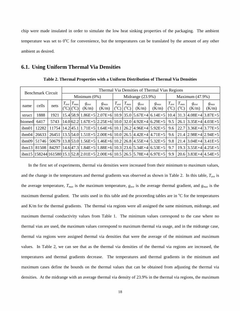
Table 2. Thermal Properties with a Uniform Distribution of Thermal Via Densities
Thermal Via Densities of Thermal Vias Regions Benchmark Circuit
Minimum (0%) Midrange (23.9%) Maximum (47.9%)
name cells nets Tave
(oC) Tmax
(oC) gave
(K/m) gmax
(K/m) Tave
(oC) Tmax
(oC) gave
(K/m)
gmax
(K/m)
Tave
(oC) Tmax
(oC) gave
(K/m)
gmax
(K/m)
struct 1888 1921 15.4 58.9 1.86E+5 2.07E+6 10.9 35.0 5.67E+4 6.14E+5 10.4 31.3 4.08E+4 3.87E+5
biomed 6417 5743 14.0 62.2 1.67E+5 2.25E+6 10.0 32.0 4.92E+4 6.29E+5 9.5 26.1 3.35E+4 4.03E+5
ibm01 12282 11754 14.2 45.1 1.71E+5 1.64E+6 10.1 26.2 4.96E+4 5.92E+5 9.6 22.7 3.36E+4 3.77E+5
ibm04 26633 26451 13.5 54.0 1.51E+5 2.00E+6 10.0 26.5 4.42E+4 4.71E+5 9.6 21.4 2.98E+4 2.94E+5
ibm09 51746 50679 13.8 53.0 1.56E+5 1.46E+6 10.2 26.8 4.55E+4 5.32E+5 9.8 21.4 3.04E+4 3.41E+5
ibm13 81508 84297 14.6 47.3 1.84E+5 1.88E+6 10.3 23.6 5.34E+4 6.53E+5 9.7 19.3 3.55E+4 4.25E+5
ibm15 158244 161580 15.1 52.8 2.01E+5 2.00E+6 10.5 26.5 5.78E+4 6.97E+5 9.9 20.6 3.83E+4 4.54E+5 In the first set of experiments, thermal via densities were increased from their minimum to maximum values,
and the change in the temperatures and thermal gradients was observed as shown in Table 2. In this table, Tave is
the average temperature, Tmax is the maximum temperature, gave is the average thermal gradient, and gmax is the
maximum thermal gradient. The units used in this table and the proceeding tables are in oC for the temperatures
and K/m for the thermal gradients. The thermal via regions were all assigned the same minimum, midrange, and
maximum thermal conductivity values from Table 1. The minimum values correspond to the case where no
thermal vias are used, the maximum values correspond to maximum thermal via usage, and in the midrange case,
thermal via regions were assigned thermal via densities that were the average of the minimum and maximum
values. In Table 2, we can see that as the thermal via densities of the thermal via regions are increased, the
temperatures and thermal gradients decrease. The temperatures and thermal gradients in the minimum and
maximum cases define the bounds on the thermal values that can be obtained from adjusting the thermal via
densities. At the midrange with an average thermal via density of 23.9% in the thermal via regions, the maximum

19
temperatures were 47.3% lower and the average temperatures were 28.3% lower than in the case where no
thermal vias were used.
The previous set of experiments demonstrate the baseline thermal improvements that can be made by using a
simple thermal via placement scheme where thermal via regions are given a uniform distribution of thermal via
densities. However, with the more sophisticated thermal via placement method from Figure 5, larger thermal
improvements can be made with fewer thermal vias and a nonuniform distribution of thermal via densities. As
will be seen in the following experiments, the thermal via placements that are generated by this algorithm lie
along a continuous curve of optimized thermal via placements between the minimum and maximum cases of
Table 2. This stems from the fact that the algorithm converges at a specific value for the internal variable, gideal,
and produces a thermal via placement that corresponds to it. This algorithm finds the point, representing a
specific thermal via placement, along this curve that satisfies the desired thermal objective.
Six objective types were examined in the following experiments: maximum thermal gradient, average
thermal gradient, maximum temperature, average temperature, maximum thermal via density, and average
thermal via density. For each of these experiments, the values obtained in the midrange case from Table 2 were
used as the desired objective values for the algorithm. These values are used only to illustrate the use and
effectiveness of this thermal via placement method, and any other values can be used as the objective as long as
they are between the values obtained at the minimum and maximum cases.
6.2. Thermal Gradient Objectives
In Figure 6, the average and maximum thermal gradients were plotted against the thermal via densities for
thermal via placements obtained using our method and a uniform distribution of thermal vias for the benchmark
circuit struct. The solid curves represent the values obtained using our thermal via placement method, and as can
be seen, these curves are significantly better than the dashed curves obtained using a uniform distribution of
thermal via densities.

20
Thermal Gradient Before and After Thermal Via Placement
3.5
7.0
10.5
14.0
17.5
21.0
24.5
0% 5% 10% 15% 20% 25% 30% 35% 40% 45%
Percent Metalization
Ave
rage
The
rmal
Gra
dien
t
(x10
4 K/m
)
-100
-50
0
50
100
150
200
Max
imum
The
rmal
Gra
dien
t
(x10
4 K/m
)
average thermal gradient with uniform metallizationaverage thermal gradient with our methodmaximum thermal gradient with uniform metallizationmaximum thermal gradient with our method
Figure 6. Thermal gradient optimization curves for struct.
In Table 3, thermal via placements were obtained using the maximum thermal gradients from the midrange
case (in Table 2) as the objectives. In this table, Kave is the average vertical thermal conductivity of the thermal
via regions, and mave is the average density of thermal vias in the thermal via regions. On average, thermal via
placements had a thermal via density of only 10.2% in the thermal via regions in order to obtain the same
maximum thermal gradients as in the midrange case. This means that 57.3% fewer thermal vias were needed
with thermal via placement than in the midrange case to obtain the same maximum thermal gradients. These
maximum thermal gradients were 68.1% lower than in the case where no thermal vias were used. In these
experiments, thermal via regions were assigned to only 10% of the total chip area, and thermal vias require only
10.2% of this area to satisfy this objective so thermal vias would occupy only 1.02% of the total chip area. With
this small amount of blockages, it is expected that routability would be minimally affected.
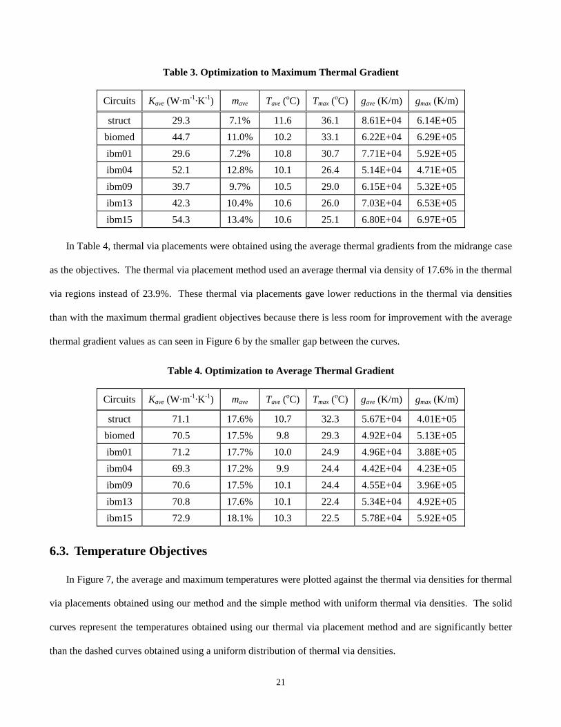
21
Table 3. Optimization to Maximum Thermal Gradient
Circuits Kave (W·m-1·K-1) mave Tave (
oC) Tmax (oC) gave (K/m) gmax (K/m)
struct 29.3 7.1% 11.6 36.1 8.61E+04 6.14E+05
biomed 44.7 11.0% 10.2 33.1 6.22E+04 6.29E+05
ibm01 29.6 7.2% 10.8 30.7 7.71E+04 5.92E+05
ibm04 52.1 12.8% 10.1 26.4 5.14E+04 4.71E+05
ibm09 39.7 9.7% 10.5 29.0 6.15E+04 5.32E+05
ibm13 42.3 10.4% 10.6 26.0 7.03E+04 6.53E+05
ibm15 54.3 13.4% 10.6 25.1 6.80E+04 6.97E+05
In Table 4, thermal via placements were obtained using the average thermal gradients from the midrange case
as the objectives. The thermal via placement method used an average thermal via density of 17.6% in the thermal
via regions instead of 23.9%. These thermal via placements gave lower reductions in the thermal via densities
than with the maximum thermal gradient objectives because there is less room for improvement with the average
thermal gradient values as can seen in Figure 6 by the smaller gap between the curves.
Table 4. Optimization to Average Thermal Gradient
Circuits Kave (W·m-1·K-1) mave Tave (
oC) Tmax (oC) gave (K/m) gmax (K/m)
struct 71.1 17.6% 10.7 32.3 5.67E+04 4.01E+05
biomed 70.5 17.5% 9.8 29.3 4.92E+04 5.13E+05
ibm01 71.2 17.7% 10.0 24.9 4.96E+04 3.88E+05
ibm04 69.3 17.2% 9.9 24.4 4.42E+04 4.23E+05
ibm09 70.6 17.5% 10.1 24.4 4.55E+04 3.96E+05
ibm13 70.8 17.6% 10.1 22.4 5.34E+04 4.92E+05
ibm15 72.9 18.1% 10.3 22.5 5.78E+04 5.92E+05
6.3. Temperature Objectives
In Figure 7, the average and maximum temperatures were plotted against the thermal via densities for thermal
via placements obtained using our method and the simple method with uniform thermal via densities. The solid
curves represent the temperatures obtained using our thermal via placement method and are significantly better
than the dashed curves obtained using a uniform distribution of thermal via densities.

22
Temperature Before and After Thermal Via Placement
10
11
12
13
14
15
16
17
18
0% 5% 10% 15% 20% 25% 30% 35% 40% 45%
Percent Metalization
Ave
rage
Tem
pera
ture
(oC
)
10
15
20
25
30
35
40
45
50
55
60
Max
imum
Tem
pera
ture
(oC
)
average temperature with uniform metallizationaverage temperature with our methodmaximum temperature with uniform metallizationmaximum temperature with our method
Figure 7. Temperature optimization curves for struct.
In Table 5, thermal via placements were obtained using the maximum temperatures from the midrange case
as the objectives. On average, the thermal via placements used only a thermal via density of 12.3% in the
thermal via regions in order to obtain maximum temperatures that are 47.3% lower than in the minimum case.
48.5% fewer thermal vias were needed than in the midrange case to obtain the same maximum temperatures.
With only 10% of the chip area assigned to thermal via regions, thermal vias would occupy only 1.23% of the
total chip area.
Table 5. Optimization to Maximum Temperature
Circuits Kave (W·m-1·K-1) mave Tave (
oC) Tmax (oC) gave (K/m) gmax (K/m)
struct 34.9 8.5% 11.4 35.0 7.97E+04 5.74E+05
biomed 50.1 12.3% 10.1 32.0 5.88E+04 5.94E+05
ibm01 57.1 14.1% 10.1 26.2 5.58E+04 4.20E+05
ibm04 51.6 12.7% 10.1 26.5 5.16E+04 4.72E+05
ibm09 51.1 12.6% 10.3 26.8 5.40E+04 4.72E+05
ibm13 59.8 14.8% 10.3 23.6 5.85E+04 5.43E+05
ibm15 46.0 11.3% 10.8 26.5 7.44E+04 7.55E+05

23
The average temperatures from the midrange case were used as the desired objective values for the results in
Table 6. With this objective, an average thermal via density of 14.3% was needed. Similar to the average
thermal gradient curves, the gap between the average temperature curves in Figure 7 show that little improvement
can be expected with the average temperature.
Table 6. Optimization to Average Temperature
Circuits Kave (W·m-1·K-1) mave Tave (
oC) Tmax (oC) gave (K/m) gmax (K/m)
struct 57.9 14.3% 10.9 32.9 6.27E+04 4.45E+05
biomed 57.0 14.1% 10.0 30.9 5.50E+04 5.64E+05
ibm01 58.0 14.3% 10.1 26.1 5.53E+04 4.16E+05
ibm04 57.2 14.1% 10.0 25.7 4.89E+04 4.55E+05
ibm09 58.2 14.4% 10.2 25.7 5.04E+04 4.41E+05
ibm13 57.7 14.3% 10.3 23.8 5.97E+04 5.54E+05
ibm15 59.1 14.6% 10.5 24.3 6.50E+04 6.67E+05
6.4. Thermal Via Density Objectives
Thermal Via Density Before and After Thermal Via Placement
0%
10%
20%
30%
40%
50%
60%
0% 5% 10% 15% 20% 25% 30% 35% 40% 45%
Percent Metalization
Max
imum
The
rmal
Via
Den
sity
maximum thermal via density with our methodmaximum thermal via density with uniform metallization
Figure 8. Maximum thermal via densities for struct.

24
The maximum thermal via densities produced using our method and the uniform thermal via density method
are plotted in Figure 8. The solid curve was obtained using our thermal via placement method, and it rapidly
increases and plateaus at the maximum value as the average thermal via density increases. The dashed curve was
obtained using a uniform distribution of thermal via densities and increases linearly as a result.
Table 7. Optimization to Maximum Thermal Via Density
Circuits mave mmax Tave (oC) Tmax (
oC) gave (K/m) gmax (K/m)
struct 3.3% 25.0% 12.6 40.9 1.14E+05 8.06E+05
biomed 3.3% 25.0% 11.5 44.8 1.01E+05 1.02E+06
ibm01 5.2% 25.0% 11.2 32.8 8.82E+04 6.85E+05
ibm04 4.1% 25.0% 11.2 36.2 8.61E+04 7.18E+05
ibm09 5.2% 25.0% 11.2 34.6 8.19E+04 6.89E+05
ibm13 4.4% 25.0% 11.6 31.4 1.02E+05 9.26E+05
ibm15 4.0% 25.0% 12.0 35.6 1.17E+05 1.07E+06 Table 7 shows the thermal via placements obtained using a maximum thermal via density of 25% (from the
midrange case) as the objective. The average thermal via densities obtained for this objective were much lower
and had an average of 4.2%. The other thermal properties were not as good as in the midrange case but were
much better than the minimum case where no thermal vias were used. With the value of 25% for the maximum
thermal via density, significant thermal improvements can be made with very little thermal via utilization. At this
point on the optimization curve, thermal via regions use only 4.2% of its area, but the maximum thermal gradient
is reduced by 55.5% and the maximum temperature is reduced by 31.4% as compared to the case where no
thermal vias are present. This objective could also be used to ensure that no thermal via regions use more
thermal vias than some specified amount that is lower than the actual maximum possible utilization.
The average thermal via density of 23.9%, same as the midrange case, was used as the desired objective
value for Table 8. As you can see, with the same average thermal via density, the thermal properties are
improved considerably over the thermal via placements with uniform thermal via densities. The results from this
will be more clearly summarized in the next section.

25
Table 8. Optimization to Average Thermal Via Density
Circuits Kave (W·m-1·K-1) mave Tave (
oC) Tmax (oC) gave (K/m) gmax (K/m)
struct 96.1 23.9% 10.5 31.7 4.89E+04 3.87E+05
biomed 96.1 23.9% 9.6 27.3 4.13E+04 4.08E+05
ibm01 96.1 23.9% 9.8 23.4 4.19E+04 3.77E+05
ibm04 96.1 23.9% 9.7 22.2 3.67E+04 3.34E+05
ibm09 96.1 23.9% 9.9 22.5 3.81E+04 3.41E+05
ibm13 96.1 23.9% 9.9 20.6 4.46E+04 4.25E+05
ibm15 96.1 23.9% 10.0 21.1 4.91E+04 4.66E+05
6.5. Comparing Different Objectives
A number of observations can be obtained from the optimization curves shown in Figures 6, 7, and 8. Not
only can the absolute improvement of thermal via placements be compared with the minimum case where no
thermal vias are present, but also the relative improvement can be seen against the simple method with uniform
thermal via densities. The thermal improvements can be observed at any average thermal via density by
comparing the curves vertically. In addition, the reduction in the average thermal via densities can observed for
any particular thermal objective by comparing the curves horizontally.
Table 9. Summary of Results for Different Objectives
Average percent change from the midrange case Objective
gmax gave Tmax Tave mmax mave
gmax 0.0% 33.5% 5.2% 3.3% 79.6% -57.3%
gave -23.3% 0.0% -8.3% -1.7% 100.0% -26.5%
Tmax -8.6% 20.9% 0.0% 1.4% 100.0% -48.5%
Tave -15.3% 11.3% -3.5% 0.0% 100.0% -40.3%
mmax 40.9% 93.3% 30.7% 12.7% 0.0% -82.4%
mave -34.5% -15.7% -14.3% -3.7% 100.0% 0.0%
The results for these six objective types are summarized in Table 9. The average percent differences between
the thermal via placement and the midrange case values are given in this table. The thermal via placement
method was very accurate in achieved the desired objective values as can be seen by the zero percents in the
diagonal. This is not surprising since ε was set to 0.001 in these experiments. When given the same average

26
thermal via density, the maximum thermal gradient is reduced by 34.5% and the maximum temperatures are
reduced by 14.3%. With the maximum thermal gradient objective, temperature values are increased only slightly,
but the thermal via densities are reduced greatly having an average reduction of 57.3%. The percent difference
between the values obtained with this method and with no thermal vias is shown in Table 10. With each case,
thermal properties are greatly improved at the expense of larger thermal via densities.
Table 10. The Results compared to the Minimum Case
Average percent change from the minimum case Objective
gmax gave Tmax Tave mmax mave
gmax -68.1% -60.8% -44.5% -25.9% 44.9% 10.2%
gave -75.7% -70.7% -51.6% -29.5% 50.0% 17.6%
Tmax -71.1% -64.5% -47.3% -27.3% 50.0% 12.3%
Tave -73.2% -67.4% -49.2% -28.3% 50.0% 14.3%
mmax -55.5% -43.3% -31.4% -19.2% 25.0% 4.2%
mave -79.2% -75.3% -54.7% -31.0% 50.0% 23.9%
6.6. Run Time
Run Time Efficiency of Thermal Via Placement Method
0
50
100
150
200
250
300
0 20000 40000 60000 80000 100000 120000 140000 160000
Number of Cells
Run
Tim
e (s
ec)
maximum temperature objectiveaverage temperature objectivemaximum thermal gradient objectiveaverage thermal gradient objectivemaximum thermal via density objectiveaverage thermal via density objective
Figure 9. Run Time Efficiency of our Method.
27
The run time efficiency of the thermal via placement algorithm was also examined in Figure 9. In this figure
we see that the thermal via placement method has linear time efficiency across a wide range of circuit sizes for all
six thermal objectives used. This is achieved by using an efficient thermal solver and because the thermal via
placement method convergences in roughly the same number of iterations.
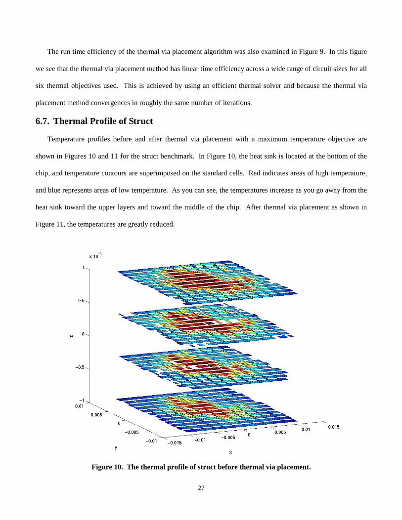
6.7. Thermal Profile of Struct Temperature profiles before and after thermal via placement with a maximum temperature objective are
shown in Figures 10 and 11 for the struct benchmark. In Figure 10, the heat sink is located at the bottom of the
chip, and temperature contours are superimposed on the standard cells. Red indicates areas of high temperature,
and blue represents areas of low temperature. As you can see, the temperatures increase as you go away from the
heat sink toward the upper layers and toward the middle of the chip. After thermal via placement as shown in
Figure 11, the temperatures are greatly reduced.
Figure 10. The thermal profile of struct before thermal via placement.

28
In Figure 11, the thermal via regions are superimposed on the resulting temperature profile after thermal via
placement is performed. Thermal via regions are represented as small squares arranged in a grid pattern. The
percentage of thermal vias in the thermal via regions is represented by its color. A red square represents a
thermal via region with maximum number of thermal vias utilized. A blue square represents a thermal via region
with minimum number of thermal vias utilized. The colored contours around the thermal via regions represent
the temperatures. The heat sink is located at the bottom, and the thermal via regions were of greatest strength at
the bottom of the chip where the thermal gradients are the highest and the most impact can be made in reducing
thermal problems. However, at the top of the chip where the temperatures are the highest, the thermal vias are
minimally used. In these areas, the thermal gradients are quite low and little impact can be made there.
Figure 11. The thermal profile and thermal vias regions of struct after thermal via placement.

29
7. CONCLUSION
An efficient thermal via placement method was presented that attempts to overcome the thermal issues
produced in the design of 3D ICs. The resulting thermal via placements have lower temperatures and thermal
gradients with minimal use of thermal vias. The method is flexible enough to handle different thermal objectives
such as obtaining a specific maximum temperature for the chip. As shown in Figures 6, 7, and 8, thermal via
placements produced by this method lie on a continuous path from the minimum to maximum cases. These
curves show significant improvement over using a uniform distribution of thermal via densities. In these
experiments, the thermal via placement method used 48.5% fewer thermal vias to reach the same 47.3%
reduction in the maximum temperatures that was obtained by given all the thermal via regions the same midrange
thermal via densities.
The method makes iterative improvements to the thermal via placement until the desired objective value is
reached. In the process, the thermal conductivities of the thermal via regions are modified in order to satisfy this
objective. Each thermal conductivity corresponds to a particular percentage of thermal vias in the thermal via
region. There is a tradeoff between thermal effects and thermal via densities as seen in Table 2. There is also a
tradeoff between area used for routing and area used for thermal vias. Consequently, this produces a tradeoff
between thermal problem reduction using thermal vias and routability. An important observation is that thermal
vias placed in areas of high temperature, such as in the upper-most layer, have little impact in reducing thermal
problems. This algorithm places thermal vias where they will have the most impact using the thermal gradient as
a guide. High temperatures can only be reduced by alleviating the high thermal gradients leading up to them.
The thermal resistance of these heat conduction paths is reducing by lowering the thermal conductivities of
elements along it.
8. REFERENCES
[1] M. Chan and P. K. Ko, “Development of a Viable 3D Integrated Circuit Technology,” Science in China, vol. 44, no. 4, pp. 241-248, August 2001.
[2] K. Banerjee, S. J. Souri, P. Kapur, and K. C. Saraswat, “3-D ICs: A Novel Chip Design for Improving Deep

30
Submicrometer Interconnect Performance and Systems-on-Chip Integration,” in Proc. of the IEEE, vol. 89, no. 5, pp. 602-633, May 2001.
[3] S. Lee, T.F. Lemczyk, and M. M. Yovanovich, “Analysis of Thermal Vias in High Density Interconnect Technology,” in 8th IEEE Semi-Therm Symposium, pp. 55-61, Feb. 1992.
[4] R.S. Li, “Optimization of Thermal Via Design Parameters Based on an Analytical Thermal Resistance Model,” in Thermal and Thermomechanical Phenomena in Electronic Systems, pp. 475-480, 1998.
[5] D. Pinjala, M.K. Iyer, Chow Seng Guan, and I.J. Rasiah, “Thermal characterization of vias using compact models,” in Proc. of the Electronics Packaging Technology Conf., pp. 144-147, Dec. 2000.
[6] T-Y Chiang, K. Banerjee, and K. C. Saraswat, “Effect of Via Separation and Low-k Dielectric Materials on the Thermal Characteristics of Cu Interconnects,” in IEEE Int. Electron Devices Meeting Tech. Digest, pp. 261-264, 2000.
[7] T-Y. Chiang, K. Banerjee, and K. C. Saraswat, "Compact Modeling and SPICE-Based Simulation for Electrothermal Analysis of Multilevel ULSI Interconnects," in Proc. of the Int. Conf. on Comput.-Aided Des., pp. 165-172, Nov. 2001.
[8] A. Rahman and R. Reif, “Thermal Analysis of Three-Dimensional (3-D) Integrated Circuits (ICs),” in Proc. of the Interconnect Technology Conf., pp. 157–159, June 2001.
[9] T-Y. Chiang, S.J. Souri, Chi On Chui, and K.C. Saraswat, “Thermal Analysis of Heterogeneous 3D ICs with Various Integration Scenarios,” in IEEE Int. Electron Devices Meeting Tech. Digest, pp. 681-684, Dec. 2001.
[10] B. Goplen and S. S. Sapatnekar, “Thermal Via Placement in 3D ICS,” in Proc. of the ACM Int. Symp. on Physical Design, pp. 167-174, 2005.
[11] B. Goplen and S. S. Sapatnekar, "Efficient Thermal Placement of Standard Cells in 3D ICs using a Force Directed Approach," in Proc. of the Int. Conf. on Comput.-Aided Des., pp. 86 - 89, Nov. 2003.
[12] D. L. Logan, A First Course in the Finite Element Method, 3rd ed., Brooks/Cole Pub. Co., 2002.
[13] www.tu-dresden.de/mwism/skalicky/laspack/laspack.html
[14] www.cbl.ncsu.edu/pub/Benchmark_dirs/LayoutSynth92
[15] http://er.cs.ucla.edu/benchmarks/ibm-place/