plasmonic nano lithography with a high scan speed contact probe
TRANSCRIPT
Plasmonic nano lithography
with a high scan speed contact probe
Yongwoo Kim, Seok Kim, Howon Jung, Eungman Lee and Jae W. Hahn*
Nano Photonics Laboratory, School of Mechanical Engineering, Yonsei University,
262 Seongsanno, Seodaemun-gu, Seoul, 120-749, Republic of Korea
Abstract: We demonstrate plasmonic lithography with an optical contact probe to achieve high speed patterning without external gap distance control between the probe and the photoresist. The bottom surface of the probe is covered with a 10 nm thickness silica glass film for the gap distance control and coated with self-assembled monolayer (SAM) to reduce friction between the probe and the photoresist. We achieve a patterning resolution of ~50 nm and a patterning speed of ~10 mm/s. We obtain the quality of line patterning comparable to that in conventional optical lithography.
©2009 Optical Society of America
OCIS codes: (110.4235) Nanolithography; (220.4241) Nanostructure fabrication; (210.4245) Near-field optical recording; (240.6680) Surface plasmons; (250.5403) Plasmonics.
References and links
1. G. J. Leggett, “Scanning near-field photolithography--surface photochemistry with nanoscale spatial resolution,” Chem. Soc. Rev. 35(11), 1150–1161 (2006).
2. J. Loos, “The Art of SPM: Scanning probe microscopy in materials science,” Adv. Mater. 17(15), 1821–1833 (2005).
3. S. Sun, and G. J. Leggett, “Matching the resolution of electron beam lithography by scanning near-field photolithography,” Nano Lett. 4(8), 1381–1384 (2004).
4. B. W. Muir, A. Fairbrother, T. R. Gengenbach, F. Rovere, M. A. Abdo, K. M. McLean, and P. G. Hartley, “Scanning probe nanolithography and protein patterning of low-fouling plasma polymer multilayer films,” Adv. Mater. 18(23), 3079–3082 (2006).
5. I. Suez, M. Rolandi, S. A. Backer, A. Scholl, A. Doran, D. Okawa, A. Zettl, and J. M. J. Fréchet, “High-field scanning probe lithography in hexadecane: transitioning from field induced oxidation to solvent decomposition through surface modification,” Adv. Mater. 19(21), 3570–3573 (2007).
6. Y. Lin, M. H. Hong, W. J. Wang, Y. Z. Law, and T. C. Chong, “Sub-30 nm lithography with near-field scanning optical microscope combined with femtosecond laser,” Appl. Phys., A Mater. Sci. Process. 80(3), 461–465 (2005).
7. J. W. Kingsley, S. K. Ray, A. M. Adawi, G. J. Leggett, and D. G. Lidzey, “Optical nanolithography using a scanning near-field probe with an integrated light source,” Appl. Phys. Lett. 93(21), 213103 (2008).
8. M. M. Alkaisi, R. J. Blaikie, and S. J. McNab, “Nanolithography in the evanescent near field,” Adv. Mater. 13(12-13), 877–887 (2001).
9. J. G. Goodberlet, and H. Kavak, “Patterning sub-50 nm features with near-field embedded-amplitude masks,” Appl. Phys. Lett. 81(7), 1315–1317 (2002).
10. W. Srituravanich, N. Fang, C. Sun, Q. Luo, and X. Zhang, “Plasmonic nanolithography,” Nano Lett. 4(6), 1085–1088 (2004).
11. E. X. Jin, and X. Xu, “Obtaining super resolution light spot using surface plasmon assisted sharp ridge nanoaperture,” Appl. Phys. Lett. 86(11), 111106 (2005).
12. W. L. Barnes, A. Dereux, and T. W. Ebbesen, “Surface plasmon subwavelength optics,” Nature 424(6950), 824–830 (2003).
13. C. Peng, E. X. Jin, T. W. Clinton, and M. A. Seigler, “Cutoff wavelength of ridge waveguide near field transducer for disk data storage,” Opt. Express 16(20), 16043–16051 (2008).
14. K. Sendur, and W. Challener, “Near-field radiation of bow-tie antennas and apertures at optical frequencies,” J. Microsc. 210(3), 279–283 (2003).
15. X. Shi, and L. Hesselink, “Mechanisms for enhancing power throughput from planar nano-apertures for near-field optical data storage,” Jpn. J. Appl. Phys. 41(Part 1, No. 3B), 1632–1635 (2002).
16. Z. Rao, L. Hesselink, and J. S. Harris, “High-intensity bowtie-shaped nano-aperture vertical-cavity surface-emitting laser for near-field optics,” Opt. Lett. 32(14), 1995–1997 (2007).
#116639 - $15.00 USD Received 2 Sep 2009; revised 30 Sep 2009; accepted 2 Oct 2009; published 13 Oct 2009
(C) 2009 OSA 26 October 2009 / Vol. 17, No. 22 / OPTICS EXPRESS 19476
17. I. P. Radko, V. S. Volkov, J. Beermann, A. B. Evlyukhin, T. Søndergaard, A. Boltasseva, S. I. Bozhevolnyi, “Plasmonic metasurfaces for waveguiding and field enhancement,” Laser Photon. Rev., 1–16 (2009) (to be published).
18. L. Wang, S. M. Uppuluri, E. X. Jin, and X. Xu, “Nanolithography using high transmission nanoscale bowtie apertures,” Nano Lett. 6(3), 361–364 (2006).
19. L. Wang, E. X. Jin, S. M. Uppuluri, and X. Xu, “Contact optical nanolithography using nanoscale C-shaped apertures,” Opt. Express 14(21), 9902–9908 (2006).
20. N. Murphy-DuBay, L. Wang, E. C. Kinzel, S. M. Uppuluri, X. Xu, “Nanopatterning using NSOM probes integrated with high transmission nanoscale bowtie aperture,” Opt. Express 16(4), 2584–2589 (2008).
21. Y. Wang, W. Srituravanich, C. Sun, and X. Zhang, “Plasmonic nearfield scanning probe with high transmission,” Nano Lett. 8(9), 3041–3045 (2008).
22. W. Srituravanich, L. Pan, Y. Wang, C. Sun, D. B. Bogy, and X. Zhang, “Flying plasmonic lens in the near field for high-speed nanolithography,” Nat. Nanotechnol. 3(12), 733–737 (2008).
23. K. Salaita, Y. Wang, J. Fragala, R. A. Vega, C. Liu, and C. A. Mirkin, “Massively parallel dip-pen nanolithography with 55 000-pen two-dimensional arrays,” Angew. Chem. Int. Ed. 45(43), 7220–7223 (2006).
24. F. Huo, Z. Zheng, G. Zheng, L. R. Giam, H. Zhang, and C. A. Mirkin, “Polymer pen lithography,” Science 321(5896), 1658–1660 (2008).
25. E. Lee, and J. W. Hahn, “Modeling of three-dimensional photoresist profiles exposed by localized fields of high-transmission nano-apertures,” Nanotechnology 19(27), 275303 (2008).
26. E. X. Jin, and X. Xu, “Radiation transfer through nanoscale apertures,” J. Quant. Spectrosc. Radiat. Transf. 93(1-3), 163–173 (2005).
27. M. Yan, L. Thylén, M. Qiu, and D. Parekh, “Feasibility study of nanoscaled optical waveguide based on near-resonant surface plasmon polariton,” Opt. Express 16(10), 7499–7507 (2008).
28. N. Marcuvitz, Waveguide handbook (Boston Technical Publishers, Lexington 1964). 29. K. Hattori, K. Ito, Y. Soeno, M. Takai, and M. Matsuzaki, “Fabrication of discrete track perpendicular media for
high recording density,” IEEE Trans. Magn. 40(4), 2510–2515 (2004). 30. K. Wu, T. C. Bailey, C. G. Willson, and J. G. Ekerdt, “Surface hydration and its effect on fluorinated SAM
formation on SiO2 surfaces,” Langmuir 21(25), 11795–11801 (2005). 31. C. D. Lorenz, E. B. Webb III, M. J. Stevens, M. Chandross, and G. S. Grest, “Frictional dynamics of
perfluorinated self-assembled monolayers on amorphous SiO2,” Tribol. Lett. 19(2), 93–98 (2005). 32. H. J. Lee, S. Hyun, H. J. Lee, D. G. Choi, D. I. Lee, and E. S. Lee, “Adhesion promoter and anti-sticking layer
effects on adhesion properties using symmetric AFM probe,” Adv. Mater. Res. 26–28, 1113–1116 (2007). 33. G. Y. Jung, Z. Li, W. Wu, Y. Chen, D. L. Olynick, S. Y. Wang, W. M. Tong, and R. S. Williams, “Vapor-phase
self-assembled monolayer for improved mold release in nanoimprint lithography,” Langmuir 21(4), 1158–1161 (2005).
34. S. Kwon, W. Chang, and S. Jeong, “Shape and size variations during nanopatterning of photoresist using near-field scanning optical microscope,” Ultramicroscopy 105(1-4), 316–323 (2005).
1. Introduction
Optical lithography has played a key role in the progress of the semiconductor industry over the past several decades because of its high productivity. Lithography methods currently used in manufacturing nano-scale devices are mainly based on optical technology using equipment that is widely used in many industrial processes. Optical lithography has progressed by pushing the optical resolution limit to allow production of high-density electronic devices. The optical resolution, which indicates the imaging performance of an optical lithography system, is limited by the intrinsic property of light diffraction. To overcome the diffraction limit, a number of research efforts have been devoted to developing new techniques based on near field lithography [1–10]. Recent discovery of extraordinary transmission of light through a perforated metal film [11–17] has offered new possibilities for optical lithography with a high-intensity near field generated by the metal nano-aperture. Lithography systems using such high-transmission nano-apertures have achieved resolution below the diffraction limit, and have initiated the development of new schemes of plasmonic nanolithography to transfer arbitrary nano-patterns [18–21].
To realize high optical resolution, the gap distance between the aperture and photoresist (PR) should be precisely maintained in the range of a few tens of nanometers, since the coupling of the near field is extremely sensitive to the gap distance. In addition to this difficulty, a main drawback of near-field lithography is low throughput of the patterning.
A pioneering method to improve the throughput was recently reported by Srituravanich et al. [22]. They fabricated a four-by-four plasmonic lens array attached to a hard-disk head
#116639 - $15.00 USD Received 2 Sep 2009; revised 30 Sep 2009; accepted 2 Oct 2009; published 13 Oct 2009
(C) 2009 OSA 26 October 2009 / Vol. 17, No. 22 / OPTICS EXPRESS 19477
aerodynamically floated 20 nm above the rotating disk and demonstrated a patterning speed of 12 m/s. However, we expect that this floating method still has barrier of precise gap distance control with a larger area head for extending to an array probe system.
To rapidly pattern nano-scale, molecule-based features in a contact printing manner, parallel processes with two-dimensional cantilever arrays or with flexible polymer pen arrays for dip-pen lithography have been demonstrated [23,24]. The parallel process with a pen array was only intended for an array pattern of the same structure, since each pen of the array could not be separately activated. In order to produce nano-scale patterns of larger scale, we need a probe array whose elements can be separately activated.
Using an array of nano-aperture probes in a parallel process is a promising way to realize high-throughput, near-field optical lithography. However, it is difficult in practice to implement an optical probe array holding thousands or millions of elements for near field recording, since the gap distance between each probe and the substrate to be patterned should be accurately maintained in the range of tens of nanometers. To solve this issue, we propose an array of optical probes to be scanned in contact mode, which can assure a uniform nano-scale gap distance between each probe and the substrate without any active control unit. Each optical probe has an additional solid thin film layer underneath the aperture so that it can physically contact the substrate, maintaining the gap distance during the scanning.
As a proof of concept, we have designed and fabricated a contact optical probe which has a bowtie-shaped high-transmission nano-aperture in an aluminum thin film. The aperture is covered with a dielectric protection layer which maintains the gap distance between the probe and substrate in the nanometer range. We test the performance of this contact optical probe for near field patterning. Line width and depth are plotted as a function of exposure dose and compared to the corresponding curves calculated by near field pattern modeling. We evaluate the quality of line-width and depth uniformities of the line patterns in order to extend this method to the practical application of plasmonic lithography. Finally, high speed line patterning is demonstrated to test the performance of plasmonic lithography with the contact probe.
2. Design of plasmonic contact probe
For plasmonic lithography in contact mode, we have designed an optical probe holding a high-transmission, bowtie-shaped nano-aperture in a metal film. To protect the aperture from contamination and abrasion, the optical probe is filled with a dielectric material in the hole and covered with a dielectric protection layer whose thickness is governed by the gap distance between the probe and substrate.
We calculate electric field distributions in a bowtie-shape aperture in an aluminum film (for Al, ε = −22.413 + 4.410i, Lorentz-Drude model) at a wavelength of 405 nm with an x-axis polarized incident beam using FDTD (finite differential time domain) program (OptiFDTD ver. 8.0) to simulate the realistic process of patterning on a photoresist (PR). The intensity of incident plane wave is assumed to be 1 (V/m)2. The dielectric medium is silica glass (SiO2, ε = 2.25) which is transparent in the wavelength range and easily coated with by plasma-enhanced chemical vapor deposition (PECVD).
We compare the results of FDTD calculations for the two different designs of the optical apertures, one in air (the aperture and gap material is air) and one in silica glass (the aperture is filled with silica glass and gap is formed by same material) (Fig. 1). We set the ridge gap at 20 nm, which is the fabrication resolution of the focused ion beam (FIB) device. The thickness of the protection layer is 10 nm so that the field distribution can make a smooth, round spot of a minimum size [25]. Compared to the aperture in air, the aperture in silica glass with same dimension shows a shorter guide wavelength and longer cutoff wavelength [26–28]. To fit the TE10 mode, an aperture should be shrunken for dielectric filled design. We therefore adjust the outline dimension of the bowtie aperture from 200 nm to 140 nm to obtain the highest transmission of the aperture and the smallest spot size. The dimensions and
#116639 - $15.00 USD Received 2 Sep 2009; revised 30 Sep 2009; accepted 2 Oct 2009; published 13 Oct 2009
(C) 2009 OSA 26 October 2009 / Vol. 17, No. 22 / OPTICS EXPRESS 19478
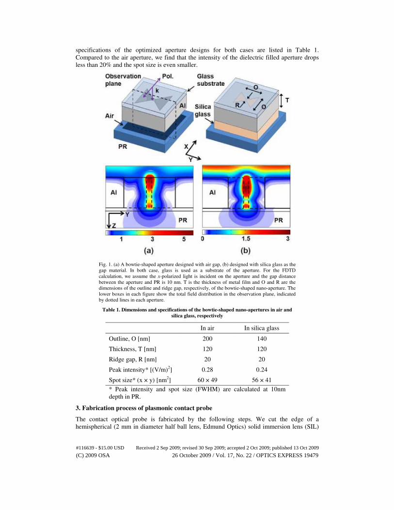
specifications of the optimized aperture designs for both cases are listed in Table 1. Compared to the air aperture, we find that the intensity of the dielectric filled aperture drops less than 20% and the spot size is even smaller.
Fig. 1. (a) A bowtie-shaped aperture designed with air gap, (b) designed with silica glass as the gap material. In both case, glass is used as a substrate of the aperture. For the FDTD calculation, we assume the x-polarized light is incident on the aperture and the gap distance between the aperture and PR is 10 nm. T is the thickness of metal film and O and R are the dimensions of the outline and ridge gap, respectively, of the bowtie-shaped nano-aperture. The lower boxes in each figure show the total field distribution in the observation plane, indicated by dotted lines in each aperture.
Table 1. Dimensions and specifications of the bowtie-shaped nano-apertures in air and
silica glass, respectively
In air In silica glass
Outline, O [nm] 200 140
Thickness, T [nm] 120 120
Ridge gap, R [nm] 20 20
Peak intensity* [(V/m)2] 0.28 0.24
Spot size* (x × y) [nm2] 60 × 49 56 × 41
* Peak intensity and spot size (FWHM) are calculated at 10nm depth in PR.
3. Fabrication process of plasmonic contact probe
The contact optical probe is fabricated by the following steps. We cut the edge of a hemispherical (2 mm in diameter half ball lens, Edmund Optics) solid immersion lens (SIL)
#116639 - $15.00 USD Received 2 Sep 2009; revised 30 Sep 2009; accepted 2 Oct 2009; published 13 Oct 2009
(C) 2009 OSA 26 October 2009 / Vol. 17, No. 22 / OPTICS EXPRESS 19479
to make a conical shape with a diamond turning machine (DTM), leaving a flat surface in 30 µm diameter on top. Additionally, FIB (SII SMI3050) milling is used for a small contact area with 3 µm diameter top surface. To maintain intimate contact with the sample, the surface quality (roughness) of the probe is an important feature. The rms (root-mean-square) roughness of the flat surface measured with an atomic force microscope (AFM, PSIA XE-100) is ~1 nm. An Al film of 120 nm thickness is coated on the flat surface using ion beam assisted thermal evaporation. A thin Cr layer of 2 nm thickness is added to ensure the adhesion of the Al film and the glass substrate. After depositing the Al film, we illuminate the surface of the Al film with the low-energy ion beam in argon to make the rms surface roughness less than 2 nm.
Bowtie nano-apertures designed in this work are formed on the metal film by FIB under 30 kV acceleration voltage, 1 pA current and 5 µs dwell time. To fill the nano-aperture with the dielectric material, we deposit a 300 nm thick silica glass film atop the metal film holding the aperture using PECVD (Oxford Instrument Plasma-lab Plus 80) at 300 °C with gas mixture (SiH4/He: 170 sccm + N2O: 710 sccm) and 670 Å/min deposition rate [29]. To obtain a good quality silica glass film, special care must be taken to maintain constant process conditions of temperature, gas mixture, and deposition rate.
In order to use the silica glass film not only for protection from contamination of the aperture but also for control of the gap between the contact probe and PR, we reduce thickness of the silica glass film from 300 nm to 10 nm using FIB milling. By observing a 10 nm thick tungsten marker which is formed on Al film before the deposition of silica glass, we detect endpoint of the milling process to fit the thickness of remained silica glass. We run the optimized process under the conditions of 30 kV acceleration voltages, 690 pA current and dwell time of 50 µs to avoid the deposition of debris due to secondary sputtering.
Finally, vapor deposition is used to apply a 1H, 1H, 2H, 2H-perfluorooctyltrichlorosilane self-assembled monolayer (SAM) to the bottom of the silica film, which reduces stiction and friction by a factor of ten in the contact between the SiO2 layer and PR [30–33]. We find that 10 nm-depth scratches are produced by the scanning probe when we apply a load of 65 µN on the contact probe without SAM coating. When SAM is applied on the bottom surface of the contact probe, however, no scratches are produced even though we apply a load of 325 µN on the contact probe.
4. Experimental setup
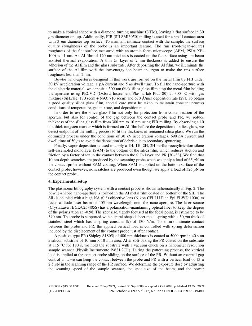
The plasmonic lithography system with a contact probe is shown schematically in Fig. 2. The bowtie-shaped nano-aperture is formed in the Al metal film coated on bottom of the SIL. The SIL is coupled with a high NA (0.8) objective lens (Nikon CFI LU Plan Epi ELWD 100×) to focus a diode laser beam of 405 nm wavelength onto the nano-aperture. The laser source (CrystaLaser, BCL-025-405S) has a polarization-maintaining optical fiber to keep the degree of the polarization at ~0.98. The spot size, tightly focused at the focal point, is estimated to be 340 nm. The probe is supported with a spiral-shaped sheet metal spring with a 50 µm thick of stainless steel which has a spring constant (k) of 130 N/m. To ensure intimate contact between the probe and PR, the applied vertical load is controlled with spring deformation induced by the displacement of the contact probe just after contact.
A positive type PR (Shipley S1805) of 400 nm thickness is coated at 5000 rpm in 40 s on a silicon substrate of 10 mm × 10 mm area. After soft-baking the PR coated on the substrate at 115 °C for 180 s, we hold the substrate with a vacuum chuck on a nanometer resolution sample scanner (Physik Instrumente P-621.2CL). During the patterning process, the vertical load is applied at the contact probe sliding on the surface of the PR. Without an external gap control unit, we can keep the contact between the probe and PR with a vertical load of 13 ± 2.5 µN in the scanning range of the PR surface. We determine the exposure dose by adjusting the scanning speed of the sample scanner, the spot size of the beam, and the power
#116639 - $15.00 USD Received 2 Sep 2009; revised 30 Sep 2009; accepted 2 Oct 2009; published 13 Oct 2009
(C) 2009 OSA 26 October 2009 / Vol. 17, No. 22 / OPTICS EXPRESS 19480
illuminated on the nano-aperture. The exposed patterns are developed in a developing solution (MF CD-26) for 10 s.
Fig. 2. Schematic of the plasmonic lithography system with a contact probe. The contact probe is fabricated in a 120 nm thick aluminum thin film. The aperture hole is filled with silica glass and covered with a 10 nm thick silica glass film for maintaining constant gap distance between the aperture and PR. A SAM is coated on the bottom surface of the silica glass to reduce friction.
5. Experiment results
5.1 High resolution line pattern
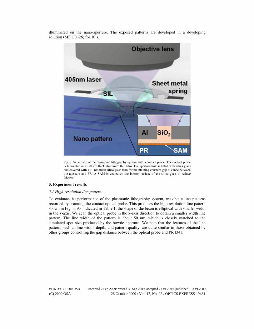
To evaluate the performance of the plasmonic lithography system, we obtain line patterns recorded by scanning the contact optical probe. This produces the high resolution line pattern shown in Fig. 3. As indicated in Table 1, the shape of the beam is elliptical with smaller width in the y-axis. We scan the optical probe in the x-axis direction to obtain a smaller width line pattern. The line width of the pattern is about 50 nm, which is closely matched to the simulated spot size produced by the bowtie aperture. We note that the features of the line pattern, such as line width, depth, and pattern quality, are quite similar to those obtained by other groups controlling the gap distance between the optical probe and PR [34].
#116639 - $15.00 USD Received 2 Sep 2009; revised 30 Sep 2009; accepted 2 Oct 2009; published 13 Oct 2009
(C) 2009 OSA 26 October 2009 / Vol. 17, No. 22 / OPTICS EXPRESS 19481
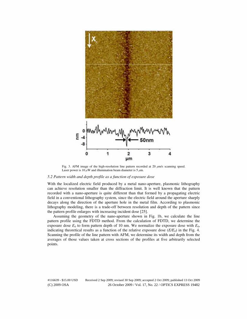
Fig. 3. AFM image of the high-resolution line pattern recorded at 20 µm/s scanning speed. Laser power is 10 µW and illumination beam diameter is 5 µm.
5.2 Pattern width and depth profile as a function of exposure dose
With the localized electric field produced by a metal nano-aperture, plasmonic lithography can achieve resolution smaller than the diffraction limit. It is well known that the pattern recorded with a nano-aperture is quite different than that formed by a propagating electric field in a conventional lithography system, since the electric field around the aperture sharply decays along the direction of the aperture hole in the metal film. According to plasmonic lithography modeling, there is a trade-off between resolution and depth of the pattern since the pattern profile enlarges with increasing incident dose [25].
Assuming the geometry of the nano-aperture shown in Fig. 1b, we calculate the line pattern profile using the FDTD method. From the calculation of FDTD, we determine the exposure dose E0 to form pattern depth of 10 nm. We normalize the exposure dose with E0, indicating theoretical results as a function of the relative exposure dose (E/E0) in the Fig. 4. Scanning the profile of the line pattern with AFM, we determine its width and depth from the averages of those values taken at cross sections of the profiles at five arbitrarily selected points.
#116639 - $15.00 USD Received 2 Sep 2009; revised 30 Sep 2009; accepted 2 Oct 2009; published 13 Oct 2009
(C) 2009 OSA 26 October 2009 / Vol. 17, No. 22 / OPTICS EXPRESS 19482
Fig. 4. Width and depth of line patterns plotted as a function of relative exposure dose (E/E0). In the experiments, we set the scan speed at 20 µm/s with illumination beam diameter of 5 µm and change the laser power from 10 to 40 µW.
In Fig. 4, we plot the width and depth of the line pattern recorded at several different exposure doses. We also calculate width and depth using plasmonic lithography modeling, indicated by the solid and dotted curves, respectively, in the same figure. The width and the depth of the experimental line patterns qualitatively follow the calculated curves, although there are small discrepancies. We presume that small imperfections in the fabrication of the metal nano-aperture may reduce transmission and cause a slightly larger spot size with smaller depth, causing the discrepancies in Fig. 4. Comparing the experimental result with the model, we obtain a threshold dose of 30.6 mJ/cm2 which indicates the minimum dose to form a pattern underneath the contact probe. The threshold dose of PR used in this work is 20 mJ/cm2 (at 405 nm wavelength), which is measured by far-field exposure tool. This means that the probe has transmission efficiency of the order of 1.
5.3 Line pattern quality evaluation
Adequate pattern quality in near-field optical lithography is one of the most important requirements for its practical application. To confirm the feasibility of plasmonic lithography as studied here, we evaluate pattern quality by measuring line width roughness (LWR), an important parameter in conventional optical lithography. Line pattern qualities are evaluated by measuring several cross sections of line patterns. We define the LWR as the standard deviation (σ) of line width and plot it as a function of mean line width in Fig. 5. Since the depth is dependent on the line width as shown in Fig. 4, we determine the depth roughness (DR) as a standard deviation (σ) of depth, also plotted in Fig. 5, in a similar manner. LWR is in the range of 4 ~ 16 nm and DR is in the range of 1 ~ 4 nm, so that LWR to line width and DR to depth are in the range of 0.05 ~ 0.20, which are comparable to those in conventional optical lithography. Figure 5 shows that the line pattern quality obtained in this work is stably maintained over a wide range of exposure doses.
#116639 - $15.00 USD Received 2 Sep 2009; revised 30 Sep 2009; accepted 2 Oct 2009; published 13 Oct 2009
(C) 2009 OSA 26 October 2009 / Vol. 17, No. 22 / OPTICS EXPRESS 19483
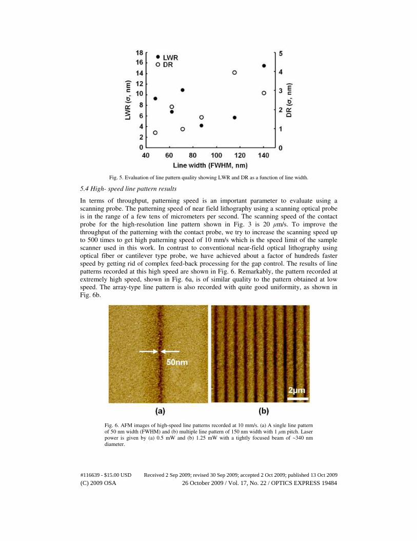
Fig. 5. Evaluation of line pattern quality showing LWR and DR as a function of line width.
5.4 High- speed line pattern results
In terms of throughput, patterning speed is an important parameter to evaluate using a scanning probe. The patterning speed of near field lithography using a scanning optical probe is in the range of a few tens of micrometers per second. The scanning speed of the contact probe for the high-resolution line pattern shown in Fig. 3 is 20 µm/s. To improve the throughput of the patterning with the contact probe, we try to increase the scanning speed up to 500 times to get high patterning speed of 10 mm/s which is the speed limit of the sample scanner used in this work. In contrast to conventional near-field optical lithography using optical fiber or cantilever type probe, we have achieved about a factor of hundreds faster speed by getting rid of complex feed-back processing for the gap control. The results of line patterns recorded at this high speed are shown in Fig. 6. Remarkably, the pattern recorded at extremely high speed, shown in Fig. 6a, is of similar quality to the pattern obtained at low speed. The array-type line pattern is also recorded with quite good uniformity, as shown in Fig. 6b.
Fig. 6. AFM images of high-speed line patterns recorded at 10 mm/s. (a) A single line pattern of 50 nm width (FWHM) and (b) multiple line pattern of 150 nm width with 1 µm pitch. Laser power is given by (a) 0.5 mW and (b) 1.25 mW with a tightly focused beam of ~340 nm diameter.
#116639 - $15.00 USD Received 2 Sep 2009; revised 30 Sep 2009; accepted 2 Oct 2009; published 13 Oct 2009
(C) 2009 OSA 26 October 2009 / Vol. 17, No. 22 / OPTICS EXPRESS 19484

5. Conclusions
We demonstrate plasmonic lithography with a contact probe to achieve high speed patterning without external control of gap distance between the probe and PR. We achieve a patterning resolution of ~50 nm and a patterning speed of ~10 mm/s. Conventional patterning speeds for optical near field recording are generally a few tens of micrometers per second. We have therefore enhanced the patterning speed by a factor of hundreds without loss of patterning resolution. To demonstrate the method’s feasibility, we evaluate the pattern quality in terms of LWR and DR, which are important parameters in the conventional optical lithography. We also demonstrate the stability of the high speed patterning process by recording a multiple line pattern to show the way to realize the high-throughput plasmonic lithography with an array of contact optical probes.
Acknowledgments
This work was supported by the Development Program of Nano Process Equipments of the Korea Ministry of Commerce, Industry and Energy. (Project no. 10030259-2008-02).
#116639 - $15.00 USD Received 2 Sep 2009; revised 30 Sep 2009; accepted 2 Oct 2009; published 13 Oct 2009
(C) 2009 OSA 26 October 2009 / Vol. 17, No. 22 / OPTICS EXPRESS 19485