plasmonics on the slope of enlightenment: the role …...plasmonics on the slope of enlightenment:...
TRANSCRIPT

Faraday DiscussionsCite this: DOI: 10.1039/c4fd00208c
PAPER
Publ
ishe
d on
04
Nov
embe
r 20
14. D
ownl
oade
d by
Pur
due
Uni
vers
ity o
n 13
/03/
2015
20:
40:0
3.
View Article OnlineView Journal
Plasmonics on the slope of enlightenment:the role of transition metal nitrides
Urcan Guler,a Alexander V. Kildishev,ab Alexandra Boltassevaab
and Vladimir M. Shalaev*ab
Received 22nd October 2014, Accepted 4th November 2014
DOI: 10.1039/c4fd00208c
The key problem currently faced by plasmonics is related to material limitations. After
almost two decades of extreme excitement and research largely based on the use of
noble metals, scientists have come to a consensus on the importance of exploring
alternative plasmonic materials to address application-specific challenges to enable the
development of new functional devices. Such a change in motivation will undoubtedly
lead to significant advancements in plasmonics technology transfer and could have a
revolutionary impact on nanophotonic technologies in general. Here, we report on one
of the approaches that, together with other new material platforms, mark an insightful
technology-driven era for plasmonics. Our study focuses on transition metal nitrides as
refractory plasmonic materials that exhibit appealing optical properties in the visible and
near infrared regions, along with high temperature durability. We take heat-assisted
magnetic recording as a case study for plasmonic technology and show that a titanium
nitride antenna satisfies the requirements for an optically efficient, durable near field
transducer paving the way to the next-generation data recording systems.
1 Introduction
It was the pioneering work by Michael Faraday that reported the “great power ofaction”metal nanoparticles have on light and the effect of parameters such as thenanoparticle dimensions on the plasmonic resonance.1 In this quintessentiallecture he described gold (Au) as “especially tted for experiments” for severalreasons mostly based on the ease of observation. Following the same reasoning,noble metals such as Au and silver (Ag) have been widely used over the last fewdecades for a broad range of activities in the eld of plasmonics.2–11 With theadvancement of nanofabrication techniques, the eld of plasmonics experienceda burst in research activities, leading to great expectations on outcomes for dailyapplications mostly associated with optics and photonics. However, between the
aNano-Meta Technologies, Inc., 1281 Win Hentschel Blvd, West Lafayette, IN 47906, USA. E-mail: uguler@
nanometatech.combSchool of Electrical and Computer Engineering and Birck Nanotechnology Center, Purdue University, West
Lafayette, IN 47907, USA. E-mail: [email protected]
This journal is © The Royal Society of Chemistry 2015 Faraday Discuss.

Faraday Discussions PaperPu
blis
hed
on 0
4 N
ovem
ber
2014
. Dow
nloa
ded
by P
urdu
e U
nive
rsity
on
13/0
3/20
15 2
0:40
:03.
View Article Online
pioneering report of Faraday and the hype in the eld, it was the electron beamtechniques that revealed plasmonic resonances of metals. In 1959, Powell andSwan reported the observation of bulk and surface plasmon resonances from analuminium (Al) thin lm via electron energy loss spectroscopy (EELS).12 As a lowcost material with plasmon resonance covering the UV and visible regions, Al isagain attracting the attention of the plasmonics community.13
Although other traditional metals, such as copper and aluminium,14,15 havebeen utilized for plasmonics applications, their room temperature oxidation andstrong dependence of the resonance quality on the oxide remain limitations fortheir widespread adoption. Similarly, Ag has been claimed as the highest qualityplasmonic material that exhibits resonances through the entire visible spectrum,but the use of the material has been hindered due to strong room temperatureoxidation and suldation; both processes are signicantly enhanced when thematerial is nanostructured.16,17 The development of chemically stable and bio-compatible Ag nanostructures is an exciting challenge with intensive ongoingeffort.18,19 Among the widely used plasmonic metals, Au has attracted a signicantamount of attention due to its chemical stability and relatively good plasmonicproperties, despite the fact that the resonance quality of Au is signicantly lowercompared to Ag and Al.20 However, even this comparison of Au against Ag showsthat the parochial approach, which concentrates simply on the resonator strengthwhen evaluating materials, could be misleading in a particular application. Infact, the entire eld of plasmonics has reached a stage where the overall func-tional material properties should be considered instead of plasmonics-onlyevaluations.
2 Assessment
As a research eld that has attracted great attention over the last two decades,giving birth to numerous application proposals, plasmonics is now subject togrand expectations on the deliverables. Relying on the maturity of the eld andthe fact that technology products are soon expected, here we discuss the briefhistory of breakthroughs and the current state of the technology from our inter-pretation of the Gartner Hype Cycle Methodology (HCM). The HCM has beensuccessfully used for a variety of technologies over the last decade and claims tobe an efficient way to adopt them to real industrial problems.21
Fig. 1 shows the authors' view on the main milestones in plasmonics that havegenerated a great deal of attention over the past decade. Although the rstobservations of plasmonic effects are quite old,22 the systematic investigation ofthe interaction of light with nanoscale metallic particles clearly starts with thework performed by Faraday in 19th century.1 Aer a relatively long period oftheoretical studies performed by leading scientists,23,24 the characterization ofelectron-beam-excited plasmons are considered the leading experimental effortsin the eld.12,25 Surface enhanced Raman scattering (SERS), rst observed in 1974by Martin Fleischmann et al.26 and attributed to enhanced electric eld by DavidJeanmaire and Richard Van Duyne in 1977,27 is perhaps the very rst systematicapplication of plasmonic effects. Soon aer the rst experimental results werereported, the clear relation between the localized surface plasmon resonance(LSPR) and the enhanced SERS signal was proposed by Martin Moskovits.28,29
With the advancement of nanofabrication methods and their widespread
Faraday Discuss. This journal is © The Royal Society of Chemistry 2015

Fig. 1 The hype cycle for the field of plasmonics from the authors' point of view. After adecade of high expectations, material limitations are delaying the realization of theproposed concepts and technology transfer. Merging plasmonics with materials scienceand chemistry could provide new solutions and bring technological advances across manyapplication spaces.
Paper Faraday DiscussionsPu
blis
hed
on 0
4 N
ovem
ber
2014
. Dow
nloa
ded
by P
urdu
e U
nive
rsity
on
13/0
3/20
15 2
0:40
:03.
View Article Online
availability, breakthrough results such as the extraordinary transmission of lightthrough plasmonic nanoholes,30 and plasmonic metamaterials created a strongimpact.31
Sensing and biomedical applications have long been the agship of the elddue to the wide range of exciting opportunities offered by bio-compatible, plas-monic nanostructures.32–34 With a solid research record over the past two decades,a wide variety of sensing and biomedical devices based on plasmonic effects wereexpected to enter production lines. However, technology transfer has thus farbeen slow compared to the level of expectations.35 Beyond biomedical applica-tions, interest in the eld was substantially nourished by several recent proposalsto develop sub-wavelength, hybrid nanophotonic components that have opticaland electronic functionalities,4,9,36–49 and plasmonic photovoltaics where metalnanoparticles were used as E-eld concentrators in thin lm devices for enhancedphotocurrent generation.50–54
In our opinion, the peak of expectations in the eld of plasmonics was reachedwith the breakthrough concept of spaser,55 the plasmonic counterpart of a laser atnanoscale, that could potentially be the key towards many nanoscale applicationssuch as all-optical circuitry, lithography, probing and microscopy.56,57 Thecompensation of losses in plasmonic nanostructures with semiconductorquantum dots,58 and a demonstration of a spaser based on sub-wavelengthresonators made of gold nanoparticles surrounded by a dye-doped silica shelloperating in the visible spectrum were reported soon aer the proposal.59
However, despite extensive experimental efforts, losses in metal nanostructuresarising from electron scattering have been the major limiting factor for the spaserand the eld of plasmonics in general.60,61 This absorption of electromagneticenergy due to material losses is inherently affecting technologies relying on the
This journal is © The Royal Society of Chemistry 2015 Faraday Discuss.

Faraday Discussions PaperPu
blis
hed
on 0
4 N
ovem
ber
2014
. Dow
nloa
ded
by P
urdu
e U
nive
rsity
on
13/0
3/20
15 2
0:40
:03.
View Article Online
eld enhancement and lossless propagation of energy, which span the entire listof breakthroughs positioned at the peak of expectations.
The metamaterials research, a eld highly correlated with plasmonics, hasfollowed a similar trend over the last decade. Triggered by the negative indexmaterials and superlens,31,62–64 excitement and expectations peaked with the ideaof cloaking and transformation optics.65,66 In the authors' opinion, aer therecognition of material limitations such as losses and scalability, the eld isexperiencing an enlightenment period with approaches incorporating alternativematerials with realistic design parameters.
We believe the breakthroughs that led to the peak of somewhat inatedexpectations are now evolving and bringing solutions to earlier problems. Forexample, the concept of harvesting solar energy using the enhanced interaction ofplasmonic nanostructures with light has expanded to the generation of hotelectrons for efficient heating, and plasmon induced photocatalysis.67,68 Mubeenet al. recently reported an approach where metal in a plasmonic photovoltaicdevice is not a eld enhancing antenna as in previous concepts, but instead, playsthe role of the light absorber that generates carriers.69 Another approach to beatthe metallic losses is to use high refractive index dielectric nanostructures as lighttrappers.70 Nanophotonic circuitry is now leaning towards the integration ofplasmonics with newly emerging research on 2D materials such as graphene andMoS2 and quantum photonics.71–74 Plasmonic metamaterials research isconcentrated on alternative materials with application specic characteristicssuch as low loss, tunability, refractory properties, and CMOS compatibility.37,75–77
Research into alternative materials for spectral ranges out of the visible are otherexamples of application-specic efforts in the eld of plasmonics.78,79 In thiswork, we consider one of the approaches that, together with other new materialplatforms including semiconductors, 2D materials, phase-changing and ceramicmaterials, marks an insightful technology-driven era for plasmonics on the slopeof enlightenment.
3 Results & discussions
In this paper, we report on a case study for plasmonics technology that couldenable the next-generation of data recording systems. In particular, we focus onthe potential of refractory plasmonic materials as nanoantennas for eldenhancement and local heating. Refractory plasmonic materials provide twounique properties: good plasmonic performance in the visible and near infraredregions, and durability at high temperatures.76 Although the denition varies withthe level of devoutness, we will use the term refractory to describe materials withmelting points above 2000 �C. Mechanical hardness and chemical stability areother common features of refractory materials, while metals with refractoryproperties generally suffer from oxidation at high temperatures.80 Thus, oxidationis considered as an exception to chemical inertness when classifying refractorymetals. Self-passivation of the oxide slows down the process for bulk metals, butnanoscale structures are oen too small to accommodate a protective oxide layer.
In contrast to structural deformations such as melting and creep that areusually encountered in the case of so metals, oxidation of refractory plasmonicmaterials can be avoided with the integration of optically transparent materialswith higher oxidation temperatures. Thus, for applications with extreme
Faraday Discuss. This journal is © The Royal Society of Chemistry 2015
Paper Faraday DiscussionsPu
blis
hed
on 0
4 N
ovem
ber
2014
. Dow
nloa
ded
by P
urdu
e U
nive
rsity
on
13/0
3/20
15 2
0:40
:03.
View Article Online
operational conditions, refractory plasmonic materials with comparable opticalproperties can replace noble metals,81 with the help of optically transparent,oxidation resistant thin layers, and new technologies can be developed.
Refractory metals provide high melting temperatures and hardness along withmetallic properties that imply their potential use for plasmonic applications. Theyhave been the material of choice where metallic optical properties and hightemperature stability are desired such as spectrally selective photonic crystalemitters for thermophotovoltaic devices.82,83 However, for applications whereenhanced interaction of a sub-wavelength structure with electromagnetic radia-tion is essential, the requirements go beyond the metallic behaviour and neces-sitate good plasmonic properties.77 Although the metrics for a good plasmonicmaterial are functions of a variety of parameters mostly depending on theapplication,84 it is usually considered acceptable to reduce the formulation tosimplied terms.77,85 Here, we will limit the discussion to LSPR where nano-particles are employed as sub-wavelength eld enhancers. One such applicationwhich has been quite popular over the last few years is the heat assisted magneticrecording (HAMR).86 In the HAMR approach, magnetic grains made of highcoercivity materials, which require an intense magnetic eld to be written, arelocally heated in order to facilitate the writing process. The requirement of a highcoercivity material is simply a result of the motivation to achieve higher densitydata storage, which causes the use of smaller grains and introduces instabilities.86
Aer the writing is accomplished at an elevated temperature, the grain is cooleddown to lower temperatures where it can retain the data. It was initially proposedthat local heating could be achieved under focused laser illumination.87 Despite asuccessful demonstration, laser heating was naturally limited by the diffractionlimit which resulted in a spot much larger than the sizes imposed by the densestorage motivation.
In order to achieve sub-wavelength focusing of electromagnetic radiation,plasmonic nanostructures can be used in the system as near eld transducers(NFTs).86 In this scenario, the excitation light is guided onto a plasmonic nano-structure with a resonance around 830 nm, where cost-effective diode lasers areavailable, and the enhanced near-eld is used as a concentrated source of energyfor local heating of the magnetic layer. Noble metals are the natural candidatesfor NFTs as they exhibit strong plasmonic oscillations in the visible region of theelectromagnetic spectrum. Although the plasmonic properties of silver (Ag) aresuperior to Au, chemical instability and consequent performance degradation is amajor concern for HAMR and many other applications. Therefore, owing to itschemical stability, Au was used as the plasmonic NFT material in the very rstdemonstrations of HAMR technology where the idea has been successfullydemonstrated.88,89 However, Au is a somaterial with a relatively low bulk meltingtemperature which is further reduced due to the nanostructured geometries andsharpened edges required for better eld connement.90 Although operationaltemperatures around 400 �C are required at the nanoscale near the magneticgrain, NFTs made of pure Au show degradation in their mechanical properties attemperatures around 100 �C.91 The mechanical instability of Au NFTs underconditions imposed by HAMR's operational principles has been one of the majorproblems which has slowed the progress towards a reliable product.92 Amongseveral methods to resolve the problem, alloying and doping of the plasmonicNFT material with a harder dopant, at the expense of lowered optical
This journal is © The Royal Society of Chemistry 2015 Faraday Discuss.

Faraday Discussions PaperPu
blis
hed
on 0
4 N
ovem
ber
2014
. Dow
nloa
ded
by P
urdu
e U
nive
rsity
on
13/0
3/20
15 2
0:40
:03.
View Article Online
performance, have attracted attention.91,93 Although refractory metals can be usedas the hard dopants to improve the mechanical properties of plasmonic metals,their use as the plasmonic NFT material has so far not been possible due to pooroptical properties.
Transition metal nitrides are refractory materials with highmelting points andmechanical hardnesses. They have been widely used as protective coatings inapplications where mechanical strength is desired. In addition to their superiormechanical properties, it has been demonstrated that titanium nitride (TiN) andzirconium nitride (ZrN) exhibit plasmonic properties similar to Au, explainingtheir golden luster.84,94,95 In fact, these materials have been used in imitationjewellery as a cheaper andmore durable replacement for Au.96 As a bio-compatiblematerial, the use of TiN is common in bio-medical implants.97,98 Consequently,TiN has been one of the most frequently used transition metal nitrides which hasresulted in a good understanding of the deposition techniques, including CMOScompatible processes.99,100 The optical properties of transition metal nitridesstrongly depend on the deposition conditions and can be optimized to nearlymatch the optical properties of Au.84,101,102
Fig. 2 shows the real and imaginary parts of the dielectric permittivities ofdifferent metals along with transition metal nitrides. Gold is presented as areference since it has been widely used as the plasmonic material in manyapplications, including in HAMR demonstrations. Here we use permittivitiesexperimentally retrieved from Au thin lms deposited on a sapphire substrate asdescribed elsewhere.95 Although the permittivities reported by Johnson andChristy are frequently used in comparison tables, in practice, thin lms of metalsexhibit optical properties that are inferior to bulk values.103,104 Transition metalnitride lms were also experimentally retrieved from thin lms deposited onsapphire and MgO substrates while the permittivities of refractory metals weretaken from tabulated data.77,95,105 Not surprisingly, the magnitude of the real part(30) is largest for the case of Au. In addition, the imaginary part of the permittivity(30 0) is also one of the smallest among the materials listed. The use of Au as theNFT material would be unquestionable if the plasmonic properties were the only
Fig. 2 Dielectric permittivities of refractory transitionmetal nitrides, refractory metals, andgold. Gold is given as a reference plasmonic material. Transition metal nitrides, which arerefractory materials that are durable at high temperatures, exhibit optical properties similarto gold. Refractory metals, on the other hand, are plasmonic in the near infrared regionand exhibit larger losses.
Faraday Discuss. This journal is © The Royal Society of Chemistry 2015

Paper Faraday DiscussionsPu
blis
hed
on 0
4 N
ovem
ber
2014
. Dow
nloa
ded
by P
urdu
e U
nive
rsity
on
13/0
3/20
15 2
0:40
:03.
View Article Online
concern. However, as stated earlier, the ductility of Au prevents the use of thematerial for a long period without further processing which degrades its opticalproperties. On the other hand, refractory metals, which would naturally resolvemany issues related to material deformations, do not exhibit plasmonic proper-ties in the spectral region of interest. Tungsten (W) and molybdenum (Mo) arebarely plasmonic in the infrared region, however their permittivities are positivein the visible region. Tantalum (Ta), on the other hand, has a permittivity zerocross-over near 610 nm, making the material plasmonic around HAMR opera-tional wavelengths. However, the imaginary part of the permittivity is stillsignicantly higher that Au, although it is much smaller than other refractorymetals. For the case of transition metal nitrides, the optical properties are closerto plasmonic metals – representing a signicant opportunity to resolve thecomplications arising due to the harsh operational environment. Both the 30 and30 0 values of ZrN are very close to Au, especially in the visible region, making it apotential candidate to replace noble metals. Fig. 2 presents three different sets ofTiN data retrieved from samples grown on sapphire and MgO. Sapphire supportslocal epitaxial growth of TiN and reduces the losses in the lm while MgOprovides better lattice matching, leading to an even higher quality epitaxial thinlm. Titanium nitride lms grown on sapphire substrates have a negativepermittivity in the visible region and a loss factor in the same range as the Au lm.Thin lms of TiN deposited on MgO substrates exhibit plasmonic propertiesbetter than the sample grown on sapphire.
The gure of merit (FOM) of a plasmonic nanostructure totally depends on thespecic application in mind.77 The high level of interest in identifying properplasmonic materials has resulted in a comprehensive collection of reportscomparing different material classes for metamaterial, transformation optics,superlens, surface plasmon polariton and LSPR applications.77,106–108 The generalconsensus for LSPR applications is to set the ratio of the real and imaginary parts ofthe dielectric permittivity of a plasmonic material as a FOM.77,106–108 For a nano-particle in the quasistatic limit, when the size of the particle is very small comparedto the wavelength, the FOM can be conveniently dened as 30/30 0 where the real partof permittivity implies a good resonator and the imaginary part represents the lossfactor. However, as the particle size becomes comparable to the wavelength of theincident light, the quasistatic approximation loses its validity, and so does the FOM.A straight modication to increase the accuracy of the FOM is to include the sizefactor which would take into account missing effects such as the existence of thehigher order modes, interference effects arising from the multi-modal system,penetration depth of the excitation light through the nanoparticle, etc. In addition,even for the case of a single eld such as LSPR, there are a variety of operationalmodes which require different features such as maximized absorption in theparticle and subsequent efficient local heating or hot electron generation,11,109
enhanced eld in the near zone for energy connement,59,110 or scattering to the farzone for several other applications.111,112 Previously we have shown that a morecomprehensive, yet still convenient, FOM for LSPR applications is the optical cross-section which can be obtained through theMie formalism.84 A comparison betweenthe scattering efficiencies of transition metal nitrides and Au shows that the eldenhancement at the surface, or at an innite distance from the particle, for TiN andZrN are indeed comparable to Au when the nanoparticles are out of the quasistaticregime.84 Here, we will follow the general consensus and apply the simplied FOM
This journal is © The Royal Society of Chemistry 2015 Faraday Discuss.

Faraday Discussions PaperPu
blis
hed
on 0
4 N
ovem
ber
2014
. Dow
nloa
ded
by P
urdu
e U
nive
rsity
on
13/0
3/20
15 2
0:40
:03.
View Article Online
with the quasistatic approximation to compare the LSPR efficiencies of transitionmetal nitrides, refractory metals, and Au, which is the reference material due to itswide use in the eld. In HAMR technology, an NFT is expected to focus electro-magnetic energy to a conned volume in the magnetic layer with minimal loss inthe plasmonic particle itself. We note that recently reported comparisons betweentransition metal nitrides and Au employed the FOM in the quasistatic approxi-mation and TiN's optical properties that were not yet optimized for plasmonicapplications.85,113,114
Table 1 shows the dielectric permittivity values for gold, refractory metals, andrefractory transition metal nitrides at a wavelength of 830 nm. Dielectricpermittivities retrieved for TiN thin lms deposited on c-sapphire and MgOsubstrates are given to illustrate the variation of the optical properties based onthe deposition parameters, (and hence, crystallinity and the amount of defects)and their effect on the FOM. It should be noted that the comparison of the realpart to the imaginary part is reasonable due to the fact that (i) the real partillustrates the resonator properties which determines the eld enhancement, and(ii) the imaginary part factors in the losses which degrade the resonance andincrease the internal heating of the NFT, an undesired effect.85 Table 1 shows thatthe experimental data retrieved from the Au thin lm deposited on sapphiresubstrate has the best FOM among all samples. The TiN lm deposited onsapphire has a FOM value of 2.14 which is less than half of the Au lm, but stillbetter than the previously reported FOM values for TiN.114 When grown on MgO,TiN lms with enhanced optical properties can be achieved due to the betterlattice matching between the lm and the substrate which promotes epitaxialgrowth.102 The TiN samples deposited on MgO have FOMs signicantly largerthan that of the TiN sample grown on sapphire, values very close to Au. Zirconiumnitride has a large normalized real permittivity, however the FOM value isdegraded due to large losses. Refractory metals, on the other hand, are either notplasmonic in the spectral region of interest, or exhibit very poor properties, rulingthem out for LSPR applications in the visible and near infrared region of theelectromagnetic spectrum.
Table 1 Permittivity values for refractory metals, refractory transition metal nitrides andgold at 830 nm. The figure of merit is defined in the quasistatic regime. Titanium nitridesamples grown on a MgO substrate outperform other refractory materials and becomeprominent for high temperature plasmonic applications in the visible and near infraredspectrum
MaterialPermittivity(real)
Permittivity(imaginary) FOM (|30|/30 0)
Au �23.39 4.67 5.01TiN (Al2O3) �11.73 5.47 2.14TiN (MgO) [1] �15.57 3.68 4.23TiN (MgO) [2] �19.08 4.11 4.64ZrN �21.15 7.64 2.77Mo 1.43 23.16 NAW 4.21 19.41 NATa �12.89 8.15 1.58
Faraday Discuss. This journal is © The Royal Society of Chemistry 2015

Paper Faraday DiscussionsPu
blis
hed
on 0
4 N
ovem
ber
2014
. Dow
nloa
ded
by P
urdu
e U
nive
rsity
on
13/0
3/20
15 2
0:40
:03.
View Article Online
According to the FOM values given in Table 1, TiN thin lms grown on MgOsubstrates exhibit plasmonic properties close to Au, with only 16% and 7%reduction in the optical FOM. However, as a refractory plasmonic material, TiNpossesses material properties such as hardness, a high melting point, CMOS-compatibility, and chemical stability that are of signicant importance forapplications that require extreme operational conditions. Heat assisted magneticrecording, for example, is one such application that employs plasmonic elementssuccessfully, but suffers from ductile material limitations.92
Fig. 3 shows FEM simulation results for a “nanobeak antenna” that waspreviously suggested as an efficient design for near-eld generation for HAMR.115
Here we use this design in order to take a step further in the comparison betweenTiN and Au. Although the TiN lm on a MgO substrate labelled with [2] has abetter FOM, we proceed with the data from the sample [1] in our simulations. Thecalculated absorption efficiencies of the same antenna made of Au and TiN
Fig. 3 (a) Illustration of a “nanobeak antenna” design used in simulations where titaniumnitride and gold are compared. (b) The absorption efficiencies of gold and titanium nitridenanobeak antennas and the corresponding electric field magnitudes |E| confined in a 25�25 � 10 nm3 volume in the dielectric layer 5 nm below the antenna tip. Dashed arrowsindicate the corresponding scale. (c) Electric field magnitudes |E| in the dielectric layer andheat dissipation densities inside the nanoantennas for the peak wavelengths of eachmaterial; 880 nm for TiN and 800 nm for gold. Permittivity values are taken from thesample: TiN on MgO [1], as given in Fig. 2.
This journal is © The Royal Society of Chemistry 2015 Faraday Discuss.

Faraday Discussions PaperPu
blis
hed
on 0
4 N
ovem
ber
2014
. Dow
nloa
ded
by P
urdu
e U
nive
rsity
on
13/0
3/20
15 2
0:40
:03.
View Article Online
(sample on MgO [1]), and the corresponding electric eld enhancements in adielectric layer located 5 nm below the NFT are given in Fig. 3(b). Due to thecompact design of the NFT and magnetic head, overheating of the plasmonicantenna is an undesired side effect of local heating for HAMR devices.116–119
Heat generation inside the plasmonic antenna is a direct result of theabsorption of the electromagnetic energy.120 Thus, for an NFT design, large eldenhancement in the magnetic medium is desired while the absorption inside theantenna should be kept minimal. Calculations show that the identical “nano-beak” design with Au and TiN gives comparable eld enhancement in themagnetic grain and absorption in the antenna. This result is in agreement withthe FOM values given in Table 1 for the quasistatic regime. Fig. 3(c) shows theelectric eld enhancement in a dielectric layer located 5 nm below the tip of the“nanobeak” antenna. The enhanced eld peak is conned within a 25 � 25 nm2
area for both TiN and Au antennas. Power dissipation densities inside theantennas are concentrated at the corners, as expected, which illustrates theimportance of material durability on the nanometer scale. The calculation resultspresented in Fig. 3 clearly indicate that a TiN NFT would generate heating in a verysimilar way that a Au NFT does. In addition to comparable optical properties, TiNoffers hardness and high temperature durability. In fact, TiN is already a materialof interest as a diffusion barrier between the NFT and the magnetic lip.121
Therefore, a TiN NFT is a reliable solution to multiple high temperature basedproblems.
Refractory metals are dened as chemically stable at high temperatures, butthe oxidation at elevated temperatures is always an exception.80 This is a problemfor transition metal nitrides as well.122 A self-passivating thin native oxide ofthickness around 1–2 nm is present at the surface of TiN at room temperature.Two stages of oxidation, designated as initial and normal stages, were observedwith an order of magnitude difference in the rate constants.123 Further investi-gation revealed that the TiO2 changes from amorphous to crystalline in time, andfaster with higher temperatures.124 For the case of plasmonic applications, wheresubwavelength nanostructures are the building blocks, the effects of even a thinoxide layer on the performance of the plasmonic component would be signicant.The temperatures at which oxidation starts to play a signicant role are in therange where plasmonic NFTs in HAMR devices operate (�500 �C).85 Fortunately,the oxidation is easier to handle compared to other structural problems arisingfrom the soness of Au.122Here, we suggest an optically transparent, thin overcoatas an oxidation barrier which provides long term durability at elevated temper-atures.122 Dielectric ceramics are natural candidates as oxidation resistantprotective layers over plasmonic transitionmetal nitrides. Fig. 4 shows reectancemeasurements and numerical simulations for thin TiN lms grown on a c-sapphire substrate. An overcoat layer with 10 nm thickness is applied as anoxidation resistant barrier. Fig. 4(a) shows the reectance measurements of a bareTiN lm and a sample with a dielectric overcoat. The bare lm reectancematches well with the simulation where a 2 nm native oxide is included. Fig. 4(b)shows the reectance data for the protected sample aer exposure to hightemperatures in air for several hours. The sample was cooled down to roomtemperature aer each treatment for optical measurement and heated up to thenext level for further testing. The measurements show that the lm retains itsoptical properties at least up to 525 �C which is at the upper limits of proposed
Faraday Discuss. This journal is © The Royal Society of Chemistry 2015
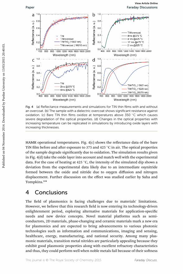
Fig. 4 (a) Reflectance measurements and simulations for TiN thin films with and withoutan overcoat. (b) The sample with a dielectric overcoat shows significant resistance againstoxidation. (c) Bare TiN thin films oxidize at temperatures above 350 �C which causessevere degradation of the optical properties. (d) Changes in the optical properties withincreasing temperature can be replicated in simulations by introducing oxide layers withincreasing thicknesses.
Paper Faraday DiscussionsPu
blis
hed
on 0
4 N
ovem
ber
2014
. Dow
nloa
ded
by P
urdu
e U
nive
rsity
on
13/0
3/20
15 2
0:40
:03.
View Article Online
HAMR operational temperatures. Fig. 4(c) shows the reectance data of the bareTiN lm before and aer exposure to 375 and 425 �C in air. The optical propertiesof the sample degrade signicantly due to oxidation. The simulation results givenin Fig. 4(d) take the oxide layer into account andmatch well with the experimentaldata. For the case of heating at 425 �C, the intensity of the simulated dip shows adeviation from the experimental data likely due to an intermediate oxynitrideformed between the oxide and nitride due to oxygen diffusion and nitrogendisplacement. Further discussion on the effect was studied earlier by Saha andTompkins.124
4 Conclusions
The eld of plasmonics is facing challenges due to materials' limitations.However, we believe that this research eld is now entering its technology-drivenenlightenment period, exploring alternative materials for application-specicneeds and new device concepts. Novel material platforms such as semi-conductors, 2D materials, phase-changing and ceramic materials mark a new erafor plasmonics and are expected to bring advancements to various photonictechnologies such as information and communications, imaging and sensing,healthcare, energy, manufacturing, and national security. Among many plas-monic materials, transition metal nitrides are particularly appealing because theyexhibit good plasmonic properties along with excellent refractory characteristicsand thus, they could perform well when noble metals fail because of their soness
This journal is © The Royal Society of Chemistry 2015 Faraday Discuss.

Faraday Discussions PaperPu
blis
hed
on 0
4 N
ovem
ber
2014
. Dow
nloa
ded
by P
urdu
e U
nive
rsity
on
13/0
3/20
15 2
0:40
:03.
View Article Online
and low melting points. In this work, we take heat assisted magnetic recording asone of the important examples of high temperature plasmonic applications andcompare the properties of refractory transition metal nitrides, refractory metals,and gold. Simulation results show that titanium nitride, in terms of its plasmonicproperties, can perform very similarly to gold but provides indispensableadvantages due to its excellent refractory characteristics. We also show that theoxidation of titanium nitride at high temperatures can be fully avoided throughthe use of optically transparent, thin ceramic overcoats. Therefore, we believe thatrefractory plasmonic transition metal nitrides are the key to next generationdurable, compact photonic devices. Our ndings directly impact the technologyof heat-assisted magnetic recording for data storage and could provide harsh-environment capable solutions for defense, intelligence, information technology,aerospace, energy, and oil & gas industries.
Acknowledgements
The authors acknowledge generous support from NSF SBIR grant IIP-1416232,ONR MURI grant N00014-10-1-0942, and NSF MRSEC grant DMR-1120923. Wewould like to thank Nathaniel Kinsey for his help in the preparation of thismanuscript.
References
1 M. Faraday, Philos. Trans. R. Soc. London, 1857, 147, 145–181.2 W. L. Barnes, A. Dereux and T. W. Ebbesen, Nature, 2003, 424, 824–830.3 E. Ozbay, Science, 2006, 311, 189–193.4 H. A. Atwater, Sci. Am., 2007, 296, 56–63.5 S. A. Maier, Plasmonics: Fundamentals and Applications, Springer, 2007.6 S. Lal, S. Link and N. J. Halas, Nat. Photonics, 2007, 1, 641–648.7 J. A. Schuller, E. S. Barnard, W. Cai, Y. C. Jun, J. S. White andM. L. Brongersma, Nat. Mater., 2010, 9, 193–204.
8 D. K. Gramotnev and S. I. Bozhevolnyi, Nat. Photonics, 2010, 4, 83–91.9 V. J. Sorger, R. F. Oulton, R.-M. Ma and X. Zhang,MRS Bull., 2012, 37, 728–738M723-710.1557/mrs.2012.1170.
10 M. Kauranen and A. V. Zayats, Nat. Photonics, 2012, 6, 737–748.11 G. Baffou and R. Quidant, Laser Photonics Rev., 2013, 7, 171–187.12 C. J. Powell and J. B. Swan, Phys. Rev., 1959, 115, 869–875.13 M. W. Knight, N. S. King, L. Liu, H. O. Everitt, P. Nordlander and N. J. Halas,
ACS Nano, 2013, 8, 834–840.14 G. H. Chan, J. Zhao, E. M. Hicks, G. C. Schatz and R. P. Van Duyne, Nano Lett.,
2007, 7, 1947–1952.15 G. H. Chan, J. Zhao, G. C. Schatz and R. P. V. Duyne, J. Phys. Chem. C, 2008,
112, 13958–13963.16 U. Guler and R. Turan, Opt. Express, 2010, 18, 17322–17338.17 M. D. McMahon, R. Lopez, H. M. Meyer, III, L. C. Feldman and R. F. Haglund,
Jr, Appl. Phys. B, 2005, 80, 915–921.18 A. Desireddy, B. E. Conn, J. Guo, B. Yoon, R. N. Barnett, B. M. Monahan,
K. Kirschbaum, W. P. Griffith, R. L. Whetten, U. Landman andT. P. Bigioni, Nature, 2013, 501, 399–402.
Faraday Discuss. This journal is © The Royal Society of Chemistry 2015

Paper Faraday DiscussionsPu
blis
hed
on 0
4 N
ovem
ber
2014
. Dow
nloa
ded
by P
urdu
e U
nive
rsity
on
13/0
3/20
15 2
0:40
:03.
View Article Online
19 G. A. Sotiriou, G. D. Etterlin, A. Spyrogianni, F. Krumeich, J.-C. Leroux andS. E. Pratsinis, Chem. Commun., 2014, 50, 13559–13562.
20 M. G. Blaber, M. D. Arnold, N. Harris, M. J. Ford and M. B. Cortie, Physica B,2007, 394, 184–187.
21 J. Fenn and M. Raskino, Mastering the Hype Cycle: How to Choose the RightInnovation at the Right Time, Harvard Business Press, 2008.
22 I. Freestone, N. Meeks, M. Sax and C. Higgitt, Gold Bull., 2007, 40, 270–277.23 G. Mie, Ann. Phys., 1908, 330, 377–445.24 J. C. M. Garnett, Philos. Trans. R. Soc., A, 1904, 203, 385–420.25 Y.-Y. Teng and E. A. Stern, Phys. Rev. Lett., 1967, 19, 511–514.26 M. Fleischmann, P. J. Hendra and A. J. McQuillan, Chem. Phys. Lett., 1974, 26,
163–166.27 D. L. Jeanmaire and R. P. Van Duyne, J. Electroanal. Chem. Interfacial
Electrochem., 1977, 84, 1–20.28 M. Moskovits, J. Chem. Phys., 1978, 69, 4159–4161.29 M. Moskovits, Notes Record Roy. Soc. Lond., 2012, 66, 195–203.30 T. W. Ebbesen, H. J. Lezec, H. F. Ghaemi, T. Thio and P. A. Wolff, Nature,
1998, 391, 667–669.31 J. B. Pendry, Phys. Rev. Lett., 2000, 85, 3966–3969.32 L. R. Hirsch, R. J. Stafford, J. A. Bankson, S. R. Sershen, B. Rivera, R. E. Price,
J. D. Hazle, N. J. Halas and J. L. West, Proc. Natl. Acad. Sci. U. S. A., 2003, 100,13549–13554.
33 C. Loo, A. Lin, L. Hirsch, M. H. Lee, J. Barton, N. Halas, J. West and R. Drezek,Technol. Cancer Res. Treat., 2004, 3, 33–40.
34 A. M. Gobin, M. H. Lee, N. J. Halas, W. D. James, R. A. Drezek and J. L. West,Nano Lett., 2007, 7, 1929–1934.
35 P. D. Howes, R. Chandrawati and M. M. Stevens, Science, 2014, 346.36 R. F. Oulton, V. J. Sorger, D. A. Genov, D. F. P. Pile and X. Zhang, Nat.
Photonics, 2008, 2, 496–500.37 A. Boltasseva and H. A. Atwater, Science, 2011, 331, 290–291.38 R. Zia, J. A. Schuller, A. Chandran and M. L. Brongersma,Mater. Today, 2006,
9, 20–27.39 M. L. Brongersma and V. M. Shalaev, Science, 2010, 328, 440–441.40 S. I. Bozhevolnyi, V. S. Volkov, E. Devaux, J.-Y. Laluet and T. W. Ebbesen,
Nature, 2006, 440, 508–511.41 T. W. Ebbesen, C. Genet and S. I. Bozhevolnyi, Phys. Today, 2008, 61, 44.42 R. Charbonneau, C. Scales, I. Breukelaar, S. Fafard, N. Lahoud, G. Mattiussi
and P. Berini, J. Lightwave Technol., 2006, 24, 477.43 A. Silva, F. Monticone, G. Castaldi, V. Galdi, A. Alu and N. Engheta, Science,
2014, 343, 160–163.44 P. Berini and I. De Leon, Nat. Photonics, 2012, 6, 16–24.45 J. R. Krenn, M. Salerno, N. Felidj, B. Lamprecht, G. Schider, A. Leitner,
F. R. Aussenegg, J. C. Weeber, A. Dereux and J. P. Goudonnet, J. Microsc.,2001, 202, 122–128.
46 K. F. MacDonald, Z. L. Samson, M. I. Stockman and N. I. Zheludev, Nat.Photonics, 2009, 3, 55–58.
47 A. G. Curto, G. Volpe, T. H. Taminiau, M. P. Kreuzer, R. Quidant and N. F. vanHulst, Science, 2010, 329, 930–933.
This journal is © The Royal Society of Chemistry 2015 Faraday Discuss.

Faraday Discussions PaperPu
blis
hed
on 0
4 N
ovem
ber
2014
. Dow
nloa
ded
by P
urdu
e U
nive
rsity
on
13/0
3/20
15 2
0:40
:03.
View Article Online
48 M. Abb, P. Albella, J. Aizpurua and O. L. Muskens, Nano Lett., 2011, 11, 2457–2463.
49 M. Staffaroni, J. Conway, S. Vedantam, J. Tang and E. Yablonovitch, PhotonicsNanostruct. Fundam. Appl., 2012, 10, 166–176.
50 H. R. Stuart and D. G. Hall, Appl. Phys. Lett., 1998, 73, 3815–3817.51 D. M. Schaadt, B. Feng and E. T. Yu, Appl. Phys. Lett., 2005, 86, 063106.52 D. Derkacs, S. H. Lim, P. Matheu, W. Mar and E. T. Yu, Appl. Phys. Lett., 2006,
89, 093103.53 H. A. Atwater and A. Polman, Nat. Mater., 2010, 9, 205–213.54 A. Polman and H. A. Atwater, Nat. Mater., 2012, 11, 174–177.55 D. J. Bergman and M. I. Stockman, Phys. Rev. Lett., 2003, 90, 027402.56 M. I. Stockman, Nat. Photonics, 2008, 2, 327–329.57 N. I. Zheludev, S. L. Prosvirnin, N. Papasimakis and V. A. Fedotov, Nat.
Photonics, 2008, 2, 351–354.58 E. Plum, V. A. Fedotov, P. Kuo, D. P. Tsai and N. I. Zheludev, Opt. Express,
2009, 17, 8548–8551.59 M. A. Noginov, G. Zhu, A. M. Belgrave, R. Bakker, V. M. Shalaev,
E. E. Narimanov, S. Stout, E. Herz, T. Suteewong and U. Wiesner, Nature,2009, 460, 1110–1112.
60 J. B. Khurgin and G. Sun, Appl. Phys. Lett., 2010, 96, 181102–181103.61 D. Pile and J. Krenn, Nat. Photonics, 2012, 6, 714–715.62 V. G. Veselago, Sov. Phys. Usp., 1968, 10, 509.63 R. A. Shelby, D. R. Smith and S. Schultz, Science, 2001, 292, 77–79.64 V. M. Shalaev, W. Cai, U. K. Chettiar, H.-K. Yuan, A. K. Sarychev, V. P. Drachev
and A. V. Kildishev, Opt. Lett., 2005, 30, 3356–3358.65 J. B. Pendry, D. Schurig and D. R. Smith, Science, 2006, 312, 1780–1782.66 U. Leonhardt, Science, 2006, 312, 1777–1780.67 O. Neumann, A. S. Urban, J. Day, S. Lal, P. Nordlander and N. J. Halas, ACS
Nano, 2012, 7, 42–49.68 S. Linic, P. Christopher and D. B. Ingram, Nat. Mater., 2011, 10, 911–921.69 S. Mubeen, J. Lee, W.-r. Lee, N. Singh, G. D. Stucky and M. Moskovits, ACS
Nano, 2014, 8, 6066–6073.70 M. L. Brongersma, Y. Cui and S. Fan, Nat. Mater., 2014, 13, 451–460.71 K. M. Goodfellow, R. Beams, C. Chakraborty, L. Novotny and A. N. Vamivakas,
Optica, 2014, 1, 149–152.72 N. P. de Leon, M. D. Lukin and H. Park, IEEE J. Sel. Top. Quantum Electron.,
2012, 18, 1781–1791.73 F. J. Garcıa de Abajo, Science, 2013, 339, 917–918.74 P. Alonso-Gonzalez, A. Y. Nikitin, F. Golmar, A. Centeno, A. Pesquera, S. Velez,
J. Chen, G. Navickaite, F. Koppens, A. Zurutuza, F. Casanova, L. E. Hueso andR. Hillenbrand, Science, 2014, 344, 1369–1373.
75 N. Strohfeldt, A. Tittl, M. Schaferling, F. Neubrech, U. Kreibig, R. Griessenand H. Giessen, Nano Lett., 2014, 14, 1140–1147.
76 U. Guler, A. Boltasseva and V. M. Shalaev, Science, 2014, 344, 263–264.77 G. V. Naik, V. M. Shalaev and A. Boltasseva, Adv. Mater., 2013, 25, 3264–3294.78 C. Langhammer, M. Schwind, B. Kasemo and I. Zoric, Nano Lett., 2008, 8,
1461–1471.79 A. Frolich and M. Wegener, Opt. Mater. Express, 2011, 1, 883–889.
Faraday Discuss. This journal is © The Royal Society of Chemistry 2015

Paper Faraday DiscussionsPu
blis
hed
on 0
4 N
ovem
ber
2014
. Dow
nloa
ded
by P
urdu
e U
nive
rsity
on
13/0
3/20
15 2
0:40
:03.
View Article Online
80 H. O. Pierson, Handbook of Refractory Carbides & Nitrides: Properties,Characteristics, Processing and Apps, William Andrew, incorporated, 1996.
81 W. Li, U. Guler, N. Kinsey, G. V. Naik, A. Boltasseva, J. Guan, V. M. Shalaev andA. V. Kildishev, Adv. Mater., 2014, 26, 7959–7965.
82 V. Rinnerbauer, Y. X. Yeng, W. R. Chan, J. J. Senkevich, J. D. Joannopoulos,M. Soljacic and I. Celanovic, Opt. Express, 2013, 21, 11482–11491.
83 K. A. Arpin, M. D. Losego, A. N. Cloud, H. Ning, J. Mallek, N. P. Sergeant,L. Zhu, Z. Yu, B. Kalanyan, G. N. Parsons, G. S. Girolami, J. R. Abelson,S. Fan and P. V. Braun, Nat. Commun., 2013, 4, 2630.
84 U. Guler, G. V. Naik, A. Boltasseva, V. M. Shalaev and A. V. Kildishev, Appl.Phys. B, 2012, 107, 285–291.
85 N. Zhou, X. Xu, T. Hammack Aaron, C. Stipe Barry, K. Gao, W. Scholz andC. Gage Edward, J. Nanophotonics, 2014, 3, 141–155.
86 M. H. Kryder, E. C. Gage, T. W. McDaniel, W. A. Challener, R. E. Rottmayer,G. Ju, Y.-T. Hsia and M. F. Erden, Proc. IEEE, 2008, 96, 1810–1835.
87 W. Challener, C. Mihalcea, C. Peng and K. Pelhos, Opt. Express, 2005, 13,7189–7197.
88 W. Challener, C. Peng, A. Itagi, D. Karns, W. Peng, Y. Peng, X. Yang, X. Zhu,N. Gokemeijer and Y.-T. Hsia, Nat. Photonics, 2009, 3, 220–224.
89 B. C. Stipe, T. C. Strand, C. C. Poon, H. Balamane, T. D. Boone, J. A. Katine,J.-L. Li, V. Rawat, H. Nemoto, A. Hirotsune, O. Hellwig, R. Ruiz, E. Dobisz,D. S. Kercher, N. Robertson, T. R. Albrecht and B. D. Terris, Nat. Photonics,2010, 4, 484–488.
90 Q. Jiang, S. Zhang and M. Zhao, Mater. Chem. Phys., 2003, 82, 225–227.91 T. Zhao, M. C. Kautzky, W. A. Challener and M. A. Seigler, U.S. Pat.,
US8427925 B2, 2013.92 N. C. Lindquist, J. Jose, S. Cherukulappurath, X. Chen, T. W. Johnson and
S.-H. Oh, Laser Photonics Rev., 2013, 7, 453–477.93 V. P. S. Rawat, B. C. Stipe, U.S. Pat., US20120127839 A1, 2012 .94 G. V. Naik, J. L. Schroeder, X. Ni, A. V. Kildishev, T. D. Sands and
A. Boltasseva, Opt. Mater. Express, 2012, 2, 478–489.95 U. Guler, J. C. Ndukaife, G. V. Naik, A. G. A. Nnanna, A. V. Kildishev,
V. M. Shalaev and A. Boltasseva, Nano Lett., 2013, 13, 6078–6083.96 Y. Nagato, U.S. Pat., 4589917, 1986.97 A. Wisbey, P. J. Gregson and M. Tuke, Biomaterials, 1987, 8, 477–480.98 S. Dong, X. Chen, L. Gu, L. Zhang, X. Zhou, Z. Liu, P. Han, H. Xu, J. Yao,
X. Zhang, L. Li, C. Shang and G. Cui, Biosens. Bioelectron., 2011, 26, 4088–4094.
99 T. E. Tang, W. Che-Chia, R. A. Haken, T. C. Holloway, L. R. Hite andT. G. W. Blake, IEEE Trans. Electron Devices, 1987, 34, 682–688.
100 H. Wakabayashi, Y. Saito, K. Takeuchi, T. Mogami and T. Kunio, IEEE Trans.Electron Devices, 2001, 48, 2363–2369.
101 G. V. Naik, J. Kim and A. Boltasseva, Opt. Mater. Express, 2011, 1, 1090–1099.102 G. V. Naik, B. Saha, J. Liu, S. M. Saber, E. A. Stach, J. M. K. Irudayaraj,
T. D. Sands, V. M. Shalaev and A. Boltasseva, Proc. Natl. Acad. Sci. U. S. A.,2014, 111, 7546–7551.
103 W. Chen, M. D. Thoreson, S. Ishii, A. V. Kildishev and V. M. Shalaev, Opt.Express, 2010, 18, 5124–5134.
This journal is © The Royal Society of Chemistry 2015 Faraday Discuss.

Faraday Discussions PaperPu
blis
hed
on 0
4 N
ovem
ber
2014
. Dow
nloa
ded
by P
urdu
e U
nive
rsity
on
13/0
3/20
15 2
0:40
:03.
View Article Online
104 M. Bosman, L. Zhang, H. Duan, S. F. Tan, C. A. Nijhuis, C. W. Qiu andJ. K. W. Yang, Sci. Rep., 2014, 4, 5537.
105 X. Ni, Z. Liu and A. V. Kildishev, 2008, http://nanohub.org/resources/3692.106 P. R. West, S. Ishii, G. V. Naik, N. K. Emani, V. M. Shalaev and A. Boltasseva,
Laser Photonics Rev., 2010, 4, 795–808.107 M. G. Blaber, M. D. Arnold and M. J. Ford, J. Phys.: Condens. Matter, 2010, 22,
143201.108 M. G. Blaber, M. D. Arnold and M. J. Ford, J. Phys. Chem. C, 2009, 113, 3041–
3045.109 C. Clavero, Nat. Photonics, 2014, 8, 95–103.110 V. M. Shalaev, AIP Conf. Proc., 2001, 560, 237–258.111 E. Stratakis and E. Kymakis, Mater. Today, 2013, 16, 133–146.112 R. Bardhan, S. Lal, A. Joshi and N. J. Halas, Acc. Chem. Res., 2011, 44, 936–946.113 B. X. Xu, Z. H. Cen, J. F. Hu and J. W. H. Tsai, J. Appl. Phys., 2015, 117, 17C112.114 T. Zhao, S. Sahoo, M. C. Kautzky, A. V. Itagi, U.S. Pat., 20130279315, 2013.115 T. Matsumoto, K. Nakamura, T. Nishida, H. Hieda, A. Kikitsu, K. Naito and
T. Koda, Appl. Phys. Lett., 2008, 93, 031108.116 S. Xiong, J. Kim, Y. Wang, X. Zhang and D. Bogy, J. Appl. Phys., 2014, 115,
17B702.117 S. Bhargava and E. Yablonovitch, Proc. SPIE, 2014, 9201.118 X. Baoxi, T. Yeow Teck, C. Cheow Wee, L. Jianming, Z. Jing, Y. Kaidong and
A. Chengwu, IEEE Trans. Magn., 2012, 48, 1789–1793.119 B. X. Xu, Z. J. Liu, R. Ji, Y. T. Toh, J. F. Hu, J. M. Li, J. Zhang, K. D. Ye and
C. W. Chia, J. Appl. Phys., 2012, 111, 07B701.120 A. O. Govorov and H. H. Richardson, Nano Today, 2007, 2, 30–38.121 J. A. Katine, V. P. S. Rawat, N. L. Robertson and B. C. Stipe, Google Patents,
2013, US8351151 B2.122 U. Guler, A. V. Kildishev, V. M. Shalaev, A. Boltasseva, D. Stocks, G. Naik, WO
Pat., PCT/US14/38561, 2014123 H. G. Tompkins, J. Appl. Phys., 1992, 71, 980–983.124 N. C. Saha and H. G. Tompkins, J. Appl. Phys., 1992, 72, 3072–3079.
Faraday Discuss. This journal is © The Royal Society of Chemistry 2015