plasticity in memristive devices for spiking neural...
TRANSCRIPT

REVIEW ARTICLEpublished: 02 March 2015
doi: 10.3389/fnins.2015.00051
Plasticity in memristive devices for spiking neural networksSylvain Saïghi1*, Christian G. Mayr2, Teresa Serrano-Gotarredona3, Heidemarie Schmidt4,
Gwendal Lecerf1, Jean Tomas1, Julie Grollier5, Sören Boyn5, Adrien F. Vincent6, Damien Querlioz6,
Selina La Barbera7, Fabien Alibart7, Dominique Vuillaume7, Olivier Bichler8, Christian Gamrat8 and
Bernabé Linares-Barranco3
1 Laboratoire d’Intégration du Matériau au Système, UMR CNRS 5218, Université de Bordeaux, Talence, France2 Institute of Neuroinformatics, University of Zurich and ETH Zurich, Zurich, Switzerland3 Instituto de Microelectrónica de Sevilla, IMSE-CNM, Universidad de Sevilla and CSIC, Sevilla, Spain4 Faculty of Electrical Engineering and Information Technology, Technische Universität Chemnitz, Chemnitz, Germany5 Unité Mixte de Physique CNRS/Thales, Palaiseau, France Associated to University Paris-Sud, Orsay, France6 Institut d’Electronique Fondamentale, Université Paris-Sud, CNRS, Orsay, France7 Institut d’Electronique, Microelectronique et Nanotechnologies, UMR CNRS 8520, Villeneuve d’Ascq, France8 CEA, LIST, Saclay Nano-INNOV PC 172, Gif sur Yvette, France
Edited by:
Themis Prodromakis, University ofSouthampton, UK
Reviewed by:
Shimeng Yu, Arizona StateUniversity, USADoo Seok Jeong, Korea Institute ofScience and Technology, SouthKoreaRonald Tetzlaff, TU Dresden,Germany
*Correspondence:
Sylvain Saïghi, Laboratoired’Intégration du Matériau auSystème, UMR CNRS 5218,Université de Bordeaux, 351 Coursde la Libération, 33405 Talence,Francee-mail: [email protected]
Memristive devices present a new device technology allowing for the realizationof compact non-volatile memories. Some of them are already in the process ofindustrialization. Additionally, they exhibit complex multilevel and plastic behaviors, whichmake them good candidates for the implementation of artificial synapses in neuromorphicengineering. However, memristive effects rely on diverse physical mechanisms, andtheir plastic behaviors differ strongly from one technology to another. Here, we presentmeasurements performed on different memristive devices and the opportunities thatthey provide. We show that they can be used to implement different learning ruleswhose properties emerge directly from device physics: real time or accelerated operation,deterministic or stochastic behavior, long term or short term plasticity. We then discusshow such devices might be integrated into a complete architecture. These results highlightthat there is no unique way to exploit memristive devices in neuromorphic systems.Understanding and embracing device physics is the key for their optimal use.
Keywords: memristive device, memristor, neuromorphic engineering, plasticity, hardware neural network
INTRODUCTIONIn 1971, Leon Chua indicated the possible existence of a fourthbasic electrical component (Chua, 1971). This component, thememristor, would complement those already known namelyresistance, capacitor, and inductor, and offer new opportunitiesfor system design (Chua and Kang, 1976). In particular, Chuaproposed to use memristors or similar memristive devices tofabricate synapses and neurons following the Hodgkin–Huxleyformalism. From this theoretical work, several publications havecited the memristive phenomenon without naming it as such andwithout linking it to Chua’s theory (Upadhyaya and Chandra,1995; Lau et al., 2004; Waser and Aono, 2007; Wu et al., 2007;Pershin and Di Ventra, 2008). HP labs were the first to recognizea device as a memristor in 2008 (Strukov et al., 2008), and theyhighlighted both the technology and its possible applications.
In parallel, the designers of the neuromorphic communityworked hard on achieving CMOS neurons to reach electri-cal energy consumption of the order of picojoule per spike(Wijekoon and Dudek, 2008; Livi and Indiveri, 2009; Ranganet al., 2010; Merolla et al., 2011; Joubert et al., 2012). However, ifthe neuron implementation still have to face important challengesto match the neurons density and functionality required for
neuromorphic circuits, the most abundant element in a neu-ral network is the synapse. Consequently, most of the effortshave been concentrated on achieving high density memories withembedded synaptic functionalities (i.e., synaptic plasticity) in asingle component. To become functional, the realization of a plas-tic synapse requires three parts: (i) synaptic weight storage, (ii)circuit for updating this weight depending on the network activ-ity, and (iii) circuit for information transmission between twoneurons. The neuromorphic community has developed a stronginterest in memristive devices because these nanodevices and theassociated integration strategies offer potential solutions to realizethese three functions.
Resistive Random Access Memory (ReRAM) technologies inits broad sense have been developed for pure memory applica-tions but can fall into the memristive system classification (Baeket al., 2004; Lee et al., 2008; Wong et al., 2012). These differenttechnologies are mostly used in binary mode and are at the stageof industrialization and commercialization (e.g., ReRAM fromPanasonic and Samsung) with high endurance, low energy, andhigh integration capability performances (Kawahara et al., 2012;Liu et al., 2013). Such performances can be an interesting plat-form for the implementation of synaptic weight storage (even
www.frontiersin.org March 2015 | Volume 9 | Article 51 | 1

Saïghi et al. Plasticity in memristive devices
in binary mode) if integration strategies and specific architec-tures are developed in order to offer a suitable solution to thelarge access required between neuron (i.e., computing node) andsynapses (memory) inherent to parallel computing in neuromor-phic circuits (and unsolved by Von Neumann architectures andassociated bottleneck). In addition, their use in analog mode(or multilevel), is the subject of great attention and could be aneffective solution for the implementation of synaptic functions.
Defining a memristor itself (see Figure 1A) can be debatable.Leon Chua now defines a memristor as any element that has anI(V) curve pinched at 0 V (Figure 1B) (Chua, 2014). This defi-nition is widely used in the literature for characterizing devices,and in this paper we synonymously use the historic word mem-ristor or the more generic “memristive device.” A general featureof memristive devices is to offer a non-volatile modification of itsresistance (or conductance) as a function of the current (charge)or voltage (flux) driving the device. In particular, neuromorphiccircuit designers prefer to think of memristors as resistive com-ponents that have the following properties: (i) the greater theelectrical charge that has passed through the component, themore the resistance value decreases, (ii) the resistance value isstored in the element even after it is turned off. Moreover, thismodification appears if the charge through the memristor goesover a “threshold” (Figure 2D).
Memristors can be realized using several technologies andwe can categorize these technologies in four large families. Thefirst includes anionic and cationic Red-Ox devices operatingon Oxidation–Reduction principles. The second is phase-changememories (PCM), where resistive switching is connected with aphysical phase change. Organic elements represent the third fam-ily. The fourth family finally comprises elements using purelyelectronic effects such as ferroelectric tunnel and spintronicmemristors. These technologies possess different behaviors andtherefore different fields of application. As part of this paper aboutsynaptic plasticity, we also point out that these technologies willlead to different plastic behaviors and learning rules. These differ-ences enrich the palette of possibilities for neuromorphic design.As Jeong et al. (2013), the purpose of this paper is not to presentan exhaustive list of memristive technology and of their associ-ated behavior, but rather to present the different forms of learningthat have been observed. In our paper, all data about memristivedevices have been measured by at least one of the co-authors.
FIGURE 1 | (A) Symbol of memristor; (B) characteristic transport featuresof memristors: pinched iv loops for different values of the maximuminjected current.
If computing and memorization principles in neural networksare not completely understood, it is now widely recognized thatlearning in such systems is associated to synaptic weight mod-ification that tends to reinforce or depress the strength of theconnection between two neurons and grouped into the wide classof synaptic plasticity. The most popular description of learningwas proposed by Hebb with the postulate “who fire together, wiretogether” (Hebb, 1949). In other words, two neurons presenting acorrelated activity will tend to reinforce their synaptic connection.A first requirement is to define what we call neuron activity: twodifferent approaches are commonly used, (i) rate coding strate-gies correspond to the definition of neuron activity as the meanfiring rate estimated on a chosen time window while (ii) temporalcoding corresponds to the assignment of neuron activity to a sin-gle spike event with a given time stamp with respect to the otherspiking neurons considered in the network. Based on this differ-ent coding strategies, variations of Hebbian learning have beenproposed such has Spike Rate Dependent Plasticity (SRDP) orthe very popular Spike Timing Dependent Plasticity (STDP). Inparticular, STDP has attracted a large interest in the memristivedevice community because of its practical implementation basedon overlapping pulses coming from the pre and post neurons.We present in Section STDP Learning Thanks to OverlappingEvents theoretical elements that allow the understanding of theapplication of this basic learning algorithm. Starting from thisideal case, we present practical implementations of STDP in solidstate devices and show how material constraint (i.e., switchingmechanism, operating conditions, . . . ) can be used to realize var-ious form of STDP. Then we present two cases of “ferroelectric”memristors based on thin film semiconductor-metal-metaloxidecompounds. These compounds were some of the first materialsto be used as memristive synapses (see Kuzum et al., 2013 for areview). The first of our ferroelectric memristors is based on sev-eral 100 nm thick BiFeO3 films experiencing resistive switching inthe Schottky barrier formed with one of the contacts. Specifically,the memristive effect in these devices is effected by a change of thedepletion layer of the Schottky diode due to a non-volatile chargetransfer similar to the “moving barrier” of TiO2. The second con-sists of ferroelectric tunnel junctions of very thin (∼1 nm) BiFeO3
films in which tunneling resistance is linked to the polarizationof the barrier. They differ radically by the time scales on whichthey operate and thus by the contexts in which they could beused. A third case based on spin-transfer torque magnetic tun-nel junction is also presented in Section Spin-Transfer TorqueMagnetic Tunnel Junction as a Stochastic Synapse. It presentsa stochastic behavior in learning which is in some ways rem-iniscent of biological neural networks. In Section SRDP withMemristive Devices, we present different form of SRDP observedin biological synapses and of interest for spike rate coding strate-gies. We first show how Short Term Plasticity, correspondingto a temporary modification of the weight that tends to relaxtoward a resting state, can be used to implement rate depen-dent modification of the weight. A second example describes howShort Term/Long Term plasticity transitions can be reproducedby taking advantage of device stability characteristics. Before theconclusion, Section Toward Memristor-CMOS Architectures andCircuits opens the discussion on the characteristics of circuit
Frontiers in Neuroscience | Neuromorphic Engineering March 2015 | Volume 9 | Article 51 | 2

Saïghi et al. Plasticity in memristive devices
FIGURE 2 | (A) Experimentally measured STDP function ξi (�T ) onbiological synapses (data from Bi and Poo, 1998, 2001). (B) Ideal STDPupdate function used in computational models of STDP synaptic
learning. (C) Anti-STDP learning function for inhibitory STDP synapses.(D) Shape of memristor weight update function f (vMR ). (E) Spikeshape waveform.
architectures that will drive memristors following their electricalbehavior.
STDP LEARNING THANKS TO OVERLAPPING EVENTSTHEORETICAL PRINCIPLESSTDP is the ability of natural or artificial synapses to changetheir strength according to the precise timing of individual pre-and/or post-synaptic spikes (Gerstner et al., 1993, 1996; Markramet al., 1997; Bi and Poo, 1998, 2001; Zhang et al., 1998; Feldman,2000; Mu and Poo, 2006; Cassenaer and Laurent, 2007; Jacobet al., 2007; Young, 2007; Finelli et al., 2008; Masquelier et al.,2008, 2009). A comprehensive overview of STDP and of its his-tory can be found elsewhere (Sjöström and Gerstner, 2010).STDP learning in biology is inherently asynchronous and on-line,meaning that synaptic incremental update occurs while neu-rons and synapses transmit spikes and perform computations inparallel. Early proposals of this used artificial time-multiplexingto alternate continuously and synchronously between “perform-ing” and “weight update” phases (Snider, 2008), thus requiringglobal system-wide synchronization. This can become a severehandicap when scaling up systems. Another option is a fullyasynchronous implementation for memristor-based STDP where“performing” and “weight update” phases happen simultane-ously in a natural manner, as in biology (Linares-Barranco andSerrano-Gotarredona, 2009a,b; Zamarreño-Ramos et al., 2011;Bichler et al., 2012b; Kuzum et al., 2012), and where there is noneed for any global synchronization.
Figure 2A shows the change of synaptic strength (in percent)measured experimentally from biological synapses as functionof relative timing �T = tpos − tpre between the arrival time tpre
of a pre-synaptic spike and the time tpos of the generation of apost-synaptic spike. Although the data shows stochasticity, wecan infer an underlying interpolated function ξ(�T) as shownin Figure 2B.
ξ (�T) ={
a+e− �Tτ+ if �T > 0
−a−e− �Tτ− if �T < 0
(1)
For a causal pre- to post-spike timing relation (�T > 0) thestrength of the synapse is increased, while for an anti-causal rela-tion (�T < 0) it is decreased. In the case of synapses with negativesynaptic strength (as in some artificial realizations), the reversedversion shown in Figure 2C can be used. Microchip CMOS cir-cuit implementations of STDP rules that follow the descriptionof Equation (1) have been reported (Indiveri et al., 2006), whichresult in about 30 transistors per plastic synapse, and thus maylead to high costs for their hardware realization. There is, over-all, general thinking that STDP is very expensive to implement inconventional CMOS microchips (Fieres et al., 2008; Khan et al.,2008). However, it can be implemented with just one memristorper synapse if appropriate peripheral signal conditioning neuronsare used in hybrid CMOS/memristor realizations.
For our purpose, we will consider a particular type of memris-tors, named voltage/flux driven memristor, which can be mathe-matically defined by.
i MR = G (w, v MR) v MR
w = f (v MR)(2)
www.frontiersin.org March 2015 | Volume 9 | Article 51 | 3

Saïghi et al. Plasticity in memristive devices
Memristor current and voltage are in general related througha non-linear conductance G (in the iMR vs. vMR plane), whoseshape is tuned by parameter w. Most of the times, however, wemay approximate the conductance as being totally linear iMR =G(w)vMR, where the value of w is dependent on the history of vMR.Parameter w represents some structural property of the memris-tor. This parameter changes non-linearly as a function f ( ) of theevolution of the memristor voltage vMR, so that the derivative ofw is governed by the second equation in (Equation 2). A typicalshape of this function is shown in Figure 2D, where a “dead zone”between two threshold voltages is present. While the memristorvoltage is kept within this dead zone, parameter w will remainconstant, and G will not change. But if the memristor voltage goesout of the dead zone, the (linear or non-linear conductance G)will change.
The STDP learning rule (as modeled by Equation 1) can, intheory, be implemented by (i) using a particular type of volt-age/flux driven memristor (Jo et al., 2010), while (ii) providingappropriately shaped pre- and post-synaptic spikes available atboth synapse (memristor) electrodes (Zamarreño-Ramos et al.,2011). For example, we can consider a pair of identical pre- andpost-synaptic spikes with a shape resembling that of biologicalspikes (see Figure 2E), with an on-set duration |t+ail| and a tail of
duration |t−ail|,
spk (t) =
⎧⎪⎪⎪⎪⎪⎪⎪⎪⎨⎪⎪⎪⎪⎪⎪⎪⎪⎩
A+mp
et
τ+ −e− t+ail
τ+
1−e− t+ail
τ+if − t+ail < t < 0
−A−mp
e− t
τ− −e− t−ail
τ−
1−e− t−ail
τ−if 0 < t < t−ail
0 if otherwise
(3)
Under these circumstances, memristor voltage is vMR(t, �t) =αpos spk(t) – αpre spk(t + �t) and synaptic strength change canbe computed as.
�w (�T) =∫
f (vMR (t,�T)) dt = ξ (�T) (4)
which has been shown to result in the same shape illustratedin Figure 2B (Zamarreño-Ramos et al., 2011). Furthermore, byreshaping the spike waveform, one can fine tune or completelyalter the STDP learning function ξ(�T), as illustrated in Figure 3.This way, by building neurons with a given degree of shape pro-grammability, it is possible to change the STDP learning functionat will, depending on the application, or make it evolve in time aslearning progresses.
Figure 4A shows a way of interconnecting memristors andCMOS neurons for STDP learning. Triangles represent the neu-ron soma, the flat side indicating its input (dendrites) and thesharp side its output (axon). Dark rectangles are memristors,each representing one synaptic junction. Every neuron controlsthe voltage at its input (Vpost in Figure 4B) and output (Vpre inFigure 4B) nodes. When the neuron is not spiking it forces a con-stant voltage at both nodes, while collecting through its inputnode the sum of input synaptic spike currents coming from the
memristors, which contribute to changing the neuron internalstate. When the neuron spikes, it sets a one-spike waveform atboth input and output nodes. This way, they send their outputspikes forward as pre-synaptic spikes for the destination synapticmemristors, but also backward to preceding synaptic memristorsas post-synaptic spikes. Zamarreño et al. showed extensive simu-lations on these concepts, and how one can change from STDPto anti-STDP by switching polarities of spikes or memristors(Zamarreño-Ramos et al., 2011). For example, (Figures 3F1,F2)illustrate the case where forward and backward spikes have oppo-site polarities, resulting in a symmetric STDP update functionξ(�T). Figures 3G1,G2 illustrate an example where forward andbackward spikes are different, with the backward spike such thatits positive part exceeds the positive memristor threshold (vth =1.0). This produces LTD (long term depression) or negative STDPupdate whenever there is a post-synaptic spike sufficiently apartfrom a pre-synaptic one; and produces LTP (long term poten-tiation) if pre- and post-synaptic spikes happen within a giventime window (Bichler et al., 2012a,b). Figures 2H1,H2 illustratea similar STDP update behavior, except that the update (whetherpositive or negative) is restricted to a limited time window.
If the system is structured into neural layers (for exam-ple, Figure 4A shows a 3-neuron-layer system) with memristivesynapses in between, then for each layer all pre-synaptic neuronsshould have the same forward spike shape and all post-synapticneurons should have the same backward shape. This way, allmemristive synapses between these two neural layers will have thesame STDP function ξ(�T).
WAVEFORM-DEFINED PLASTICITY IN FERROELECTRIC RESISTIVESWITCHING MEMRISTORSIn this section, we concentrate on an analysis of resistive switch-ing BiFeO3 (BFO). Our BFO memristors are grown by pulsedlaser deposition on Pt/Ti/SiO2/Si substrate with a circular Au topcontact (Shuai et al., 2013), see Figure 5A. The BFO films havea thickness of some 100 nm. The top contact forms a Schottkydiode, causing the created devices to show resistive switching witha rectifying behavior (Shuai et al., 2011). The devices exhibit acombination of voltage- and charge-driven behavior, and are con-sistent with the requirements of Section Theoretical Principles.When stepping DC voltages across the device, the resistance willfollow an exponential curve (Mayr et al., 2012). The voltage leveldefines the converged resistance value, while the charge passedthrough the device defines the time frame until this convergedvalue is achieved.
Resistive switching in BFO shows a number of characteris-tics which make it well-suited for use as a synapse. For instance,the dependence between voltage level and converged resistancemakes the BFO devices conform closely to the ideal waveform-driven plasticity postulated in Figure 3, as plastic changes in thememristor closely follow the overlapping pre- and post-synapticwaveforms. Up to 8 bit analog resolution can be reliably pro-grammed in the device (Shuai et al., 2013). Due to the Schottkydiode, there is also high-ohmic region up to 1 V. Similar to theparadigm of Linn et al. (2010), this can be used in an array ofBFO devices to define a voltage readout-region where only a sin-gle device in the array is active, eliminating the multiple sneak
Frontiers in Neuroscience | Neuromorphic Engineering March 2015 | Volume 9 | Article 51 | 4

Saïghi et al. Plasticity in memristive devices
FIGURE 3 | Illustration of influence of action potential shapes on the
resulting STDP memristor weight update function ξ (�T ). Memristorupper and lower thresholds are normalized to amplitudes ±1.0. From (A1,A2)
to (E1,E2) the same spike waveform travels forward and backward. In (F1,F2)
the forward and backward waveforms are the same but have opposite
polarity. In (G1,G2) to (H1,H2) the forward and backward waveforms aredifferent. In (G1,G2), the positive pulse of the backward waveform exceedsamplitude +1.0, thus producing negative STDP update whenever there is apost-synaptic spike alone (G2); otherwise if pre- and post-synaptic spikeshappen within a given time window, there will be positive STDP update.
current paths that would otherwise severely limit practical arraysize (Flocke and Noll, 2007). While this characteristic potentiallyenables large crossbar arrays of BFO devices, defect density is onthe order of 30% for an “open circuit” type failure, so a place-ment algorithm (Mayr et al., 2007) would have to be used in amemristive array to map around defect memristors.
The devices also experience a modification threshold at ca.2 V, i.e., starting from the Schottky diode threshold at 1 V up to2 V, the memristance can be measured by the current flow, butthe charge inherent in this current does not change the mem-ristance. If appropriate waveforms are chosen, the 2 V thresholdextracts pre- and post-synaptic activity correlation as memris-tance change, as postulated in Section Theoretical Principles. Allthese voltages are broadly compatible with CMOS logic processes,in contrast to other material choices that need significantly highervoltages (Kuzum et al., 2013).
The waveforms in the upper two curves of Figure 5B are usedas pre- respectively post-synaptic voltage. Those curves have notbeen shown in Figure 3; however their asymmetry is in the spiritof Figures 3G1,H1. These waveforms implement the plasticitymodel of Mayr et al. (2010), which allows for both rate- andspike-based plastic behavior. In the third curve of Figure 5B,which shows the resulting differential voltage across the memris-tor, the modification thresholds at about 2 V are marked. As canbe seen, these are crucial in permitting modification only for truepre-post coincidences (such as at 30 ms), filtering out single pre-or post-synaptic events (such as at 20 ms). The resulting synapticmodification is shown in the last curve of Figure 5B, exhibiting aclose match with the theoretical model (Mayr et al., 2010).
Measured STDP curves using this paradigm are shown inFigure 5C. With their exact reproduction of the waveform-defined exponential time window, they showcase the capability
www.frontiersin.org March 2015 | Volume 9 | Article 51 | 5

Saïghi et al. Plasticity in memristive devices
FIGURE 4 | (A) Example of Memristors and CMOS neuron circuitsarrangement for achieving STDP learning: feed-forward neural system with 3layers of neurons and two fully connecting synapse crossbars. (B) Details of
parts around one post-synaptic neuron. While a neuron is silent, it sets aconstant DC voltage at its input (Vpost ) and output (Vpre) nodes. When aneuron is sending a spike, it sets a voltage spike at both nodes.
FIGURE 5 | (A) Layout/processing of BiFeO3 devices used (Shuai et al.,2013); (B) driving voltage waveforms (from top to bottom): pre-synapticwaveform, post-synaptic waveform, resulting differential voltage acrossmemristor and resulting memristance change shown as percentage changein current through the memristor for a fixed 2 V measurement voltage(Cederstroem et al., 2013); (C) measured STDP curves for two different STDP
time window settings; time windows are adjusted via the time constants ofthe exponentials slopes of pre- and post-synaptic waveform, which changesthe LTP respectively the LTD part of the STDP window; Weight change aschange in current through the memristor; (D) measured spike triplet curves(Froemke and Dan, 2002), weight change as change in current through thememristor (Mayr et al., 2012).
of BFO synapses for fine-grained analog weights. In most cur-rent memristive materials, the STDP curves deviate significantlymore, and their time windows are primarily defined by the physi-cal device characteristics, not the driving waveform (Alibart et al.,2012; Kuzum et al., 2013). In contrast, the voltage-memristancerelationship of the BFO synapses lets them conform nicely tothe waveform-defines-plasticity paradigm postulated in theory
(Zamarreño-Ramos et al., 2011). Through this direct translationof the driving voltage waveforms into the plasticity shape, dif-ferent time windows can be easily configured via the pre- andpost-synaptic waveforms, as can be seen from the two samplecurves in Figure 5C.
By introducing adaptation into the post-synaptic waveform,specifically an exponential dependence of the post-synaptic
Frontiers in Neuroscience | Neuromorphic Engineering March 2015 | Volume 9 | Article 51 | 6

Saïghi et al. Plasticity in memristive devices
action potential duration on the inter-spike interval, the plastic-ity rule of Mayr and Partzsch (2010) is also able to reproducetriplet and rate plasticity (Froemke and Dan, 2002). When explor-ing the triplet paradigm with memristors, a faithful reproductionof biological triplet data can be seen (Figure 5D), due again tothe excellent correlation between driving waveform and evokedmemristive plasticity. The post-synaptic adaptation introducedfor triplet plasticity can be observed in the different pulse widthsin the second curve in Figure 5B (Noack et al., 2010).
Defining the plasticity entirely through the waveform can alsobe used to substantially speed up synapse behavior in BFO upto a 50 μs time scale (You et al., 2014). A switched capacitorsystem such as (Mayr et al., 2014b), if equipped with a scal-able time base (Eisenreich et al., 2009), also offers the intriguingpossibility of operating a high-density, CMOS-memristor hybridneuromorphic system at varying timescales to accommodate dif-ferent tasks, such as real-time interoperation with a visual sensorvs. offline, high-speed classification tasks where an acceleratedtimescale leads to faster classification.
HIGH-SPEED PLASTICITY IN FERROELECTRIC TUNNEL MEMRISTORS“Purely electronic” memristors are nanodevices in which theresistance changes are obtained through electron mediated phe-nomena at interfaces. These memristors promise an increasedendurance and reliability, since the material structure is pre-served, as well as a faster switching speed.
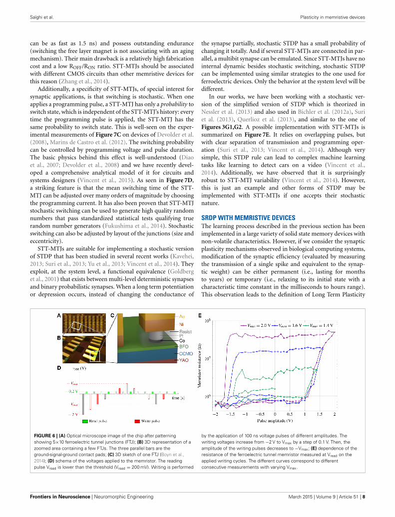
The “ferroelectric tunnel memristor” (Bibes et al., 2010)is based on an emerging digital memory concept, subject ofintense academic and industrial developments, the ferroelec-tric resistive RAM (International Technology Roadmap ForSemiconductors, 2011). Its base is the ferroelectric tunnel junc-tion (FTJ): an insulating ultrathin (several nanometers) fer-roelectric barrier sandwiched between two metallic electrodes(Figure 6A). Strain from the substrate assures that the ferroelec-tric polarization points to one of the electrodes. The polarizationcan be switched upon application of short voltage pulses andresults in resistance changes of up to several orders of mag-nitude (Garcia et al., 2009; Chanthbouala et al., 2012a). Thisresistance contrast is linked to different polarization screen-ing in the electrodes: the effective tunneling barrier heightdependents on the direction of the ferroelectric layer’s polar-ization and therefore strongly influences the tunneling current.Additionally, the strong non-linearity of the ferroelectric tunneljunction allows for a non-destructive resistance reading at low DCvoltage.
By designing the devices in such way that the switching occursthrough non-uniform ferroelectric domain configurations, quasi-analog resistance variations can be obtained (Chanthbouala et al.,2012b). A direct link between these intermediate resistance statesand the ferroelectric domain configuration allows the descriptionof its dynamic behavior through models of domain nucleationand growth in ferroelectric films. Furthermore, the cumulativebehavior upon application of trains of voltage pulses has alreadybeen demonstrated. As the polarization reversal process in theferroelectric film depends on pulse amplitude and duration,these parameters can be adapted to achieve the desired resistancechange in the memristive device—a very promising feature for the
implementation of STDP-based learning with ferroelectric tunnelmemristors (Chanthbouala et al., 2012b).
It has recently been demonstrated that fully-patterned solid-state ferroelectric tunnel memristors based on BiFeO3 (fullypatterned submicron Co/BiFeO3/Ca0.96Ce0.04MnO3 tunnel junc-tions) can be produced with high yield and with low device-to-device variations. They show resistance contrasts of more than3 orders of magnitude, can be commuted with pulses of 100 nsand amplitudes of about 2 V, and have a large endurance of over4 × 106 cycles (Boyn et al., 2014).
In Figure 6, we plot as in Yamada et al. (2013) the multi-level behavior of a ferroelectric tunnel memristor depending onapplied voltages. The curves in Figure 6B show the DC resistancevalue of the device after writing pulses of different amplitudes. Touse this memristor as a plastic synapse we consider −VMR to rep-resent the time difference �T = tpost − tpre. Then �T > 0, i.e.,VMR < 0 in Figure 6B, implies increasing conductance that cor-responds to Hebb’s rule. Conversely, �T < 0 results in a decreaseof the synaptic weight.
Choosing the waveform of Figure 3B1 for pre- and post-synaptic voltage neurons, the width of the positive square pulsecan be as low as 100 ns in the case of the ferroelectric tunnelmemristor. Accordingly, the ramp phase of the waveform will be afew times larger than this. As a result, the time difference betweenspikes for the STDP shown in Figure 3B2 can be less than 1 μs.
SPIN-TRANSFER TORQUE MAGNETIC TUNNEL JUNCTION AS ASTOCHASTIC SYNAPSESpin-Transfer Torque Magnetic Tunnel Junctions (STT-MTJs)constitute another choice to implement plastic non-volatilesynapses. They rely on a different operating mechanism thanthe devices presented in the rest of the paper, and for this rea-son are not always thought as memristive devices. Their specificstochastic behavior, however, can be particularly interesting forsynaptic applications. And as they constitute the basic cell of thesecond generation of Spin Transfer Torque Magnetic RAM (STT-MRAM)—which is currently reaching the market—, they presenta high level of CMOS compatibility and of maturity.
The basic structure of a STT-MTJ is presented in Figure 7Aand is constituted by an ensemble of layers of different materials.The magnetic “fixed” layer is a small magnet whose magnetiza-tion is pinned in one direction. The magnetic “free” layer is athinner magnet whose magnetization can be either parallel (P) orantiparallel (AP) to the one of the fixed layer. Due to the TunnelMagnetoresistance effect, the electrical resistance of the P and APstate is different. And due to the Spin Transfer Torque effect, apositive current can switch the device from AP to P state, and anegative current can switch the device from P to AP state. Thisleads to the I–V curve seen in Figure 7B, which is reminiscentof a memristive device. However, MTJs are truly binary device:AP and P states are the only possible states. Some proposals existto increase the number of states (Lou et al., 2008) or to includeanother physical effect (domain wall motion) in the MTJ toreach multilevel behavior (Wang et al., 2009; Chanthbouala et al.,2011). However, these variations do not exhibit the same degreeof maturity as binary STT-MTJs. In comparison with traditionalmemristive devices, STT-MTJs are fast to write (programming
www.frontiersin.org March 2015 | Volume 9 | Article 51 | 7
Saïghi et al. Plasticity in memristive devices
can be as fast as 1.5 ns) and possess outstanding endurance(switching the free layer magnet is not associating with an agingmechanism). Their main drawback is a relatively high fabricationcost and a low ROFF/RON ratio. STT-MTJs should be associatedwith different CMOS circuits than other memristive devices forthis reason (Zhang et al., 2014).
Additionally, a specificity of STT-MTJs, of special interest forsynaptic applications, is that switching is stochastic. When oneapplies a programming pulse, a STT-MTJ has only a probability toswitch state, which is independent of the STT-MTJ’s history: everytime the programming pulse is applied, the STT-MTJ has thesame probability to switch state. This is well-seen on the exper-imental measurements of Figure 7C on devices of Devolder et al.(2008), Marins de Castro et al. (2012). The switching probabilitycan be controlled by programming voltage and pulse duration.The basic physics behind this effect is well-understood (Diaoet al., 2007; Devolder et al., 2008) and we have recently devel-oped a comprehensive analytical model of it for circuits andsystems designers (Vincent et al., 2015). As seen in Figure 7D,a striking feature is that the mean switching time of the STT-MTJ can be adjusted over many orders of magnitude by choosingthe programming current. It has also been proven that STT-MTJstochastic switching can be used to generate high quality randomnumbers that pass standardized statistical tests qualifying truerandom number generators (Fukushima et al., 2014). Stochasticswitching can also be adjusted by layout of the junctions (size andeccentricity).
STT-MTJs are suitable for implementing a stochastic versionof STDP that has been studied in several recent works (Kavehei,2013; Suri et al., 2013; Yu et al., 2013; Vincent et al., 2014). Theyexploit, at the system level, a functional equivalence (Goldberget al., 2001) that exists between multi-level deterministic synapsesand binary probabilistic synapses. When a long term potentiationor depression occurs, instead of changing the conductance of
the synapse partially, stochastic STDP has a small probability ofchanging it totally. And if several STT-MTJs are connected in par-allel, a multibit synapse can be emulated. Since STT-MTJs have nointernal dynamic besides stochastic switching, stochastic STDPcan be implemented using similar strategies to the one used forferroelectric devices. Only the behavior at the system level will bedifferent.
In our works, we have been working with a stochastic ver-sion of the simplified version of STDP which is theorized inNessler et al. (2013) and also used in Bichler et al. (2012a), Suriet al. (2013), Querlioz et al. (2013), and similar to the one ofFigures 3G1,G2. A possible implementation with STT-MTJs issummarized on Figure 7E. It relies on overlapping pulses, butwith clear separation of transmission and programming oper-ation (Suri et al., 2013; Vincent et al., 2014). Although verysimple, this STDP rule can lead to complex machine learningtasks like learning to detect cars on a video (Vincent et al.,2014). Additionally, we have observed that it is surprisinglyrobust to STT-MTJ variability (Vincent et al., 2014). However,this is just an example and other forms of STDP may beimplemented with STT-MTJs if one accepts their stochasticnature.
SRDP WITH MEMRISTIVE DEVICESThe learning process described in the previous section has beenimplemented in a large variety of solid state memory devices withnon-volatile characteristics. However, if we consider the synapticplasticity mechanisms observed in biological computing systems,modification of the synaptic efficiency (evaluated by measuringthe transmission of a single spike and equivalent to the synap-tic weight) can be either permanent (i.e., lasting for monthsto years) or temporary (i.e., relaxing to its initial state with acharacteristic time constant in the milliseconds to hours range).This observation leads to the definition of Long Term Plasticity
FIGURE 6 | (A) Optical microscope image of the chip after patterningshowing 5×10 ferroelectric tunnel junctions (FTJ); (B) 3D representation of azoomed area containing a few FTJs. The three parallel bars are theground-signal-ground contact pads; (C) 3D sketch of one FTJ (Boyn et al.,2014); (D) schema of the voltages applied to the memristor. The readingpulse Vread is lower than the threshold (Vread = 200 mV). Writing is performed
by the application of 100 ns voltage pulses of different amplitudes. Thewriting voltages increase from −2 V to Vmax by a step of 0.1 V. Then, theamplitude of the writing pulses decreases to −Vmax; (E) dependence of theresistance of the ferroelectric tunnel memristor measured at Vread on theapplied writing cycles. The different curves correspond to differentconsecutive measurements with varying Vmax.
Frontiers in Neuroscience | Neuromorphic Engineering March 2015 | Volume 9 | Article 51 | 8

Saïghi et al. Plasticity in memristive devices
FIGURE 7 | From Vincent et al. (2014, 2015). (A) Cartoon of a Spin TransferTorque Magnetic Tunnel Junction (STT-MTJ). (B) Typical I–V curve of theSTT-MTJ. (C) Experimental measurements of stochastic switching. (D) Model
of mean switching time as a function of programming current. (E) Oursimplified STDP rule and PRE and POST overlapping pulses which implementit naturally with STT-MTJs.
(LTP) and Short Term Plasticity (STP), respectively. We can noticethat the boundary classification into Long Term (LT) and ShortTerm (ST) effects is not well-defined and should be consideredwith respect to the required task. Both STP and LTP can corre-spond to an increase or decrease of the synaptic efficiency thusleading to the definition of Short Term (Long Term) potentia-tion and depression, respectively. In biology, synaptic plasticitycan be attributed to various mechanisms involved in the trans-mission of the signal between a pre- and post-neuron, such asneurotransmitter release modification, neurotransmitter recoveryin the pre-synaptic connection, receptors sensitivity modificationor even structural modification of the synaptic connection (seeBliss and Collingridge, 1993), for a description of the differentmechanisms involved in STP and LTP). Based on this observa-tion, two important points need to be stressed. First, STP andLTP processes are not restricted to a particular learning strategy
(i.e., STDP and SRDP, for example). In this section, we presentexamples of STP and LTP processes based on a particular caseof rate coding strategy but these considerations are still valid forother coding strategies (see Alibart et al., 2012, for STDP withSTP devices). Secondly, if plasticity is intimately linked to thenotion of learning, it is important to notice that there is no one-to-one equivalence between the concepts of STP, LTP and thenotion of Short Term Memory (STM) and Long Term Memory(LTM). Indeed, even if a direct parallel has been proposed basedon the particular concept of memory consolidation (Lamprechtand Ledoux, 2004), which corresponds to accumulation of ShortTerm effect leading to Long Term memory, there are still veryimportant questions to be answered about how learning (andthe associated synaptic plasticity) is related to the memorizationof information that can also present different time scale frommilliseconds to years.
www.frontiersin.org March 2015 | Volume 9 | Article 51 | 9

Saïghi et al. Plasticity in memristive devices
FIGURE 8 | (A) Schematic of the NOMFET in a diode-like configuration. This leaky memory transistor was proposed to implement the Short Term Plasticity (B)
STP measured in biological synapses (Varela et al., 1997) and (C) STP implement in solid state device.
SHORT TERM PLASTICITY (STP)Implementation of STP has been proposed in a variety ofnanoscale memory devices. The first proposition of STP was real-ized in a nanoparticles/organic memory transistor (NOMFET)—Figure 8 (Alibart et al., 2010). The basic principle of thisdevice is equivalent to a floating gate transistor. Charges arestored in the nanoparticles and modify the channel conductiv-ity via Coulombic repulsion between the carriers (holes) andthe charged nanoparticles. The particularity of this device is topresent a leaky memory behavior: charges stored in the nanopar-ticles tend to relax with a characteristic time constant in the1–100 s range. When the NOMFET is connected in a diode likeconfiguration (Figure 8A), each input spike (with a negative volt-age value) charges the nanoparticles and decreases the NOMFETconductivity. Between pulses, charges escape from the nanopar-ticles and the conductivity relaxes toward its resting value. Byanalogy with biology, this device mimics the STP observed indepressing synapses (Figures 8B,C) and described by Abbott et al.(1997). As a matter of comparison, this synaptic functionality isrealized with a single memory transistor when its implementa-tion in Si based technologies (i.e., CMOS) required 7 transistors(Boegerhausen et al., 2003). STP has been also demonstratedin two-terminal devices that would ensure higher device den-sity when integrated into complex systems. Equivalently, STP intwo terminals devices is implemented by taking advantage of thevolatility of the different memory technologies (i.e., low retentionof the state that is often a drawback in pure memory applications).Cationic redox systems based on Electro-Chemical Memory cells(ECM) (Ohno et al., 2011) or anionic Valence Change Memory(Chang et al., 2011; Yang et al., 2013) have demonstrated STPwith a facilitating behavior. In such devices, Short Term Plasticityis ensured by the low stability of the conducting filaments that
tend to dissolve, thus relaxing the device toward the insulatingstate. TiO2 VCM cells have been reported with both facilitat-ing and depressing behavior (Lim et al., 2013) with relaxationrelated to oxidation-reduction counter reaction. Protonic deviceshave demonstrated STP with depressing functionality due toproton recovery latency from atmosphere required to restorethe proton concentration and conductivity (Josberger et al.,2014).
In the case of rate dependent plasticity, STP can be of depress-ing type (i.e., decrease of the synaptic efficiency when synapticactivity increase) or facilitating type (i.e., increase of synapticefficiency when synaptic activity increase). In terms of func-tionality, Abbott et al. (1997) has demonstrated that depressingsynapses with STP act as a gain control device (at high frequency,i.e., high synaptic activity, the synaptic weight is decreased, thusleading to a reduction of the signal when activity becomes tooimportant). More generally, STP (both depressing and facilitat-ing) provides a very important frequency coding property (asdepicted in Figures 8B,C) that could play a major role in theprocessing of spike-rate coded information. Indeed, if a simpleIntegrate and Fire neuron (I&F) is associated with static weight(with no dependence with spike frequency), the computing node(i.e., neuron and synapses) is only a linear filter (linear com-bination of the different input) while STP turns the node tonon-linear. This property can be used to implement reservoircomputing approaches as proposed by Maass (Buonomano andMaass, 2009) with the Liquid State Machine and could be animportant property of biological systems for computation.
CO-EXISTENCE OF STP AND LTP IN THE SAME DEVICEIf the contribution of ST and LT processes to computing isnot completely understood in biological systems, we should
Frontiers in Neuroscience | Neuromorphic Engineering March 2015 | Volume 9 | Article 51 | 10
Saïghi et al. Plasticity in memristive devices
consider that both STP and LTP effects in synaptic connec-tions are required in neuro-inspired computing systems. A firstapproach is to consider that repetition of short term effectsshould lead to Long Term modification in the synaptic connec-tions. This behavior would explain the important hypothesis ofmemory consolidation in the sense of psychology (Lamprechtand Ledoux, 2004). Ohno et al. (2011) reported the coexis-tence of Long Term and Short Term Potentiation in atomicbridge technology (Figure 9). Depending on pre-synaptic activity(associated to spike rate in this case), the synaptic conductiv-ity is increased due to the formation of a Ag filament acrossthe insulating gap. While for low frequency, the bridge tends torelax between pulses, higher frequencies lead to a strong fila-ment that maintains the device in the ON state. These resultssuggest a critical size of the bridging filament in order tomaintain the conductive state (i.e., providing a LTP of the synap-tic connection). Similar results have been obtained in a vari-ety of memory devices where filamentary switching displayedtwo regimes of volatility. Chang et al. (2011) have evidenceda continuous evolution of the volatility as a function of theconductivity level of the device in WO3 oxide cells attributedto the competition between oxygen vacancies drift (creation ofconductive path across the device) and lateral diffusion (dis-ruption of the conducting filaments). Another description ofthese two regimes of volatility could be associated to a compe-tition between surface and volume energies in the conductivefilament.
If this transition between Short Term Plasticity and Long TermPlasticity is intuitively well-associated to the concept of STM toLTM learning in psychology, we can note that it induces somerestriction in term of network functionality. Indeed, in biol-ogy, the facilitating process observed at short time scale andassociated to an increase of neurotransmitter release probabil-ity during a burst of spike (i.e., corresponding to an increaseof synaptic efficiency at high frequency spiking rate) is addi-tive with LTP (Bliss and Collingridge, 1993). In this case thenode (neuron and synapses) maintains its rate coding prop-erty (associated to short term process and described previouslyas a non-linear node) and can also display long term modifi-cation of the synaptic weight. Alternative approaches are stillneeded as proposed by Cantley et al. (2011) where Short Termprocesses and Long Term Processes are realized by two differ-ent devices (leaky floating gate transistor and non-volatile two-terminal devices) in order to match the complexity of biologicalsynapses. One fundamental issue that needs to be explored isthe balance between the device functionality required for properoperation of computing systems (i.e., performances) and opti-mal integration in order to match synaptic density required forcomputing.
TOWARD MEMRISTOR-CMOS ARCHITECTURES ANDCIRCUITSIn order to exploit the plasticity of memristor-based arti-ficial synapses, specific circuit architecture needs to bedeveloped. Indeed, depending on the polarity and electricalcharacteristics of investigated devices, two types of circuitshave been identified which are described in the followingparagraphs.
CIRCUITS FOR BIPOLAR MEMRISTORSMost of the works on memristive devices that have been pub-lished over the last couple of years focus on bipolar resistiveswitching devices (Waser and Aono, 2007; Snider, 2008; Strukovet al., 2008; Jo et al., 2010). This is the case for all the devicespresented in Section STDP Learning Thanks to OverlappingEvents. These devices exhibit characteristics close to the originalMemristor predicted by Chua. Their resistance can be increasedor decreased with opposite polarity voltage pulses and the resis-tance change is cumulative with the previous state of the device,which makes them particularly suitable to implement synaptic-like functionality.
A biologically-inspired spiking NN-based computingparadigm which exploits the specific physics of those devicesis presented in Querlioz et al. (2011, 2013). In this approach,CMOS input and output neurons are connected by bipolarmemristive devices used as synapses. It is natural to lay outthe nanodevices in the widely studied crossbar as illustrated onFigure 10. Learning is competitive thanks to lateral inhibitionand fully unsupervised using a simplified form of STDP.
Using this topology, performance comparable to traditionalsupervised networks has been measured (Querlioz et al., 2013)for the textbook case of character recognition, despite extremevariations of various memristive device parameters. With thesame approach, unsupervised learning of temporally correlatedpatterns from a spiking silicon retina has also been demon-strated. When tested with real-life data, the system is ableto extract complex and overlapping temporally correlated fea-tures such as car trajectories on a freeway (Bichler et al.,2012a).
CIRCUITS FOR UNIPOLAR MEMRISTORSAll that we have discussed in this work can be adapted toanother class of memristive devices—the unipolar devices whereall applied voltages to increase or decrease the resistance valueare positive. Among them, in particular, Phase-Change Memory(PCM) has good maturity, scaling capability, high endurance, andgood reliability (Fantini et al., 2010). PCM resistance can be mod-ified by applying a temporal temperature gradient modifying thematerial organization between an amorphous and a crystallinephase. The amorphous region inside the phase change layer canbe crystallized by applying set pulses, thus increasing device con-ductance. It was shown that the magnitude of the relative increasein conductance can be controlled by the pulse amplitude and bythe equivalent pulse width (Kuzum et al., 2012). Amorphization,on the other hand, is a more power-hungry process and is notprogressive with identical pulses. The current required for amor-phization is typically 5–10 times higher than for crystallization,even for state-of-the art devices.
To overcome these issues, a novel low-power architecture“2-PCM Synapse” was introduced in Bichler et al. (2012b). Theidea is to emulate synaptic functions in large scale neural net-works using two PCM devices constituting one synapse as shownin Figure 11. These two devices have an opposite contribution tothe neuron’s integration. When the synapse needs to be potenti-ated, the Long Term Potentiation (LTP) PCM device undergoesa partial crystallization, increasing the equivalent weight of thesynapse. Similarly, when the synapse must be depressed, the Long
www.frontiersin.org March 2015 | Volume 9 | Article 51 | 11

Saïghi et al. Plasticity in memristive devices
FIGURE 9 | Adapted from Ohno et al. (2011). (A) Schematic of atomicbridge devices that was proposed for Short Term Plasticity, Long TermPlasticty (STP/LTP) transition demonstration. Depending on the spiking
activity, (B) the metallic filament do not bridge the two electrodes and tendsto relax toward the OFF state while it remains (C) in the ON state once itbridges the two electrodes.
FIGURE 10 | Basic crossbar circuit topology. Wires originate from CMOS input layer (horizontal black wires) and from the CMOS output layer (vertical graywires). Memristive nanodevices are located at the cross points of the horizontal and vertical wires.
Frontiers in Neuroscience | Neuromorphic Engineering March 2015 | Volume 9 | Article 51 | 12

Saïghi et al. Plasticity in memristive devices
FIGURE 11 | Left: Experimental LTP characteristics of the unipolar PCM device. Right: Principle of an equivalent bipolar synapse realized with a 2-PCM circuit.Note that the neuron circuit is not represented on the schematic.
Term Depression (LTD) PCM device is crystallized. As the LTDdevice has a negative contribution to the neuron’s integration,the equivalent weight of the synapse is reduced. Furthermore,because gradual crystallization is achieved with successive identi-cal voltage pulses, the pulse generation is greatly simplified. Notehowever that such synaptic circuit will require a slightly morecomplex post-synaptic neuron circuit in order to deal with pulseintegration and generation. This should have a limited impacton the overall neuromorphic circuit given the lower number ofneurons vs. synapses.
DISCUSSIONMemristive devices are an appealing solution to implement plas-tic synapses, if we develop the specific driving signals to emulatedifferent learning rules. The most popular synaptic plasticityimplementation is based on the realization of Hebbian learning,and in particular of STDP. We shall however note that other plas-ticity mechanisms exist that have been studied and modeled assuggested in a recent work (Kornijcuk et al., 2014). In this paper,we focused on different implementations of STDP, by takingadvantage of the device physics of different memristive devices.The functional differences in the behaviors of the devices directlytranslate into differences in the learning rules (real time or accel-erated, deterministic or stochastic). Using other devices, we alsopresented other synaptic ideas, such as short term plasticity, orthose which exploit interactions between short term and longterm plasticity. Finally, we proposed some implementation ideas,offering a large overview of the different possibilities in severalmaterial systems.
As memristors are primarily targeted toward future high-density nanoscale arrays, CMOS driver circuits need to be scaledto these dimensions as well. That is to say, the required neuro-morphic driver circuits need to be moved to deep submicrontechnologies. One recently presented method to achieve this isthe use of switched-capacitor neuromorphic circuits, which areable to implement the required analog waveforms in high den-sity technologies as small as 28 nm (Mayr et al., 2014b). Coupled
with deep submicron CMOS sensors (Henker et al., 2007), theyoffer the possibility of a full image processing pyramid basedon memristive computation in a nanoscale CMOS-memristorhybrid. However, developing appropriate and highly scaled drivercircuits for memristive synapses which do not bring large over-heads is a significant goal for today’s research. This is especiallytrue for proposals that exploit passive crossbar integration. Suchcircuit topology is particularly appealing for neuromorphic engi-neers as it offers a direct equivalent for the neuron/synapse circuitwith high parallelism and high integration density in which a sin-gle device is associated to a single synapse between two neurons(input line and output column). However, it brings circuit chal-lenges (crosstalk, sneak path, impedance mismatch,...) that needto be overcome.
From a more systems’ perspective, the most interesting appli-cations for nanoscale memristors will be those that require alarge number of learned or programmed synaptic weights. It isimportant to already consider such applications, to understandthe true impact of memristive technology. One of these appli-cations is the Neural Engineering Framework (Eliasmith andAnderson, 2004), which can be used to implement straightfor-ward signal computation, sensor fusion (Mayr et al., 2014a), andrecognition (Bichler et al., 2012a), but also models of cognition(Eliasmith et al., 2012). The large number of synapses offered bynanoscale memristive arrays makes the implementation of com-plex cognitive processing of such large-scale models (Eliasmithet al., 2012) on a single CMOS-memristor hybrid IC a realpossibility.
Finally, it is important to understand that there are no absoluteoptimal memristive devices for the implementation of plasticityin hardware neural networks. The variety of behaviors observedin today’s research will be an advantage for neuromorphic chipdesigners and computational neuroscientists since it opens newpaths of implementation of neural computations. In this respect,the plastic behaviors measured on memristive devices and pre-sented in this paper provide the primitive for future neuromor-phic breakthroughs.
www.frontiersin.org March 2015 | Volume 9 | Article 51 | 13

Saïghi et al. Plasticity in memristive devices
ACKNOWLEDGMENTSThis paper was partly supported by funding under the EuropeanUnion Seventh Framework Programme (FP7/2007–2013) undergrant agreement no. 269459 (CORONET), no. 612058 (RAMP),no. 618024 (BAMBI), no. 318597 (SYMONE), no. 259068(NANOBRAIN), no. 604102 (HBP), under the French NationalResearch Agency under grant agreement ANR-11-NANO-0002(MHANN), ANR-13-JS03-0004 (COGNISPIN), ANR-12-PDOC-0027 (DINAMO), ANR-12-BS03-010 (SYNAPTOR),under the Spanish Ministerio de Economía y Competitividadunder ERANET grant PRI-PIMCHI-0768 (PNEUMA), underSpanish research grants (with support from the EuropeanRegional Development Fund) TEC2012-37868-C04-01(BIOSENSE), under Andalusian research grant TIC-6091(NANONEURO).
REFERENCESAbbott, L. F., Varela, J. A., Sen, K., and Nelson, S. B. (1997). Synaptic depression and
cortical gain control. Science 275, 221–224. doi: 10.1126/science.275.5297.221Alibart, F., Pleutin, S., Bichler, O., Gamrat, C., Serrano-Gotarredona, T., Linares-
Barranco, B., et al. (2012). A memristive nanoparticle/organic hybrid synap-stor for neuroinspired computing. Adv. Funct. Mater. 22, 609–616. doi:10.1002/adfm.201101935
Alibart, F., Pleutin, S., Guérin, D., Novembre, C., Lenfant, S., Lmimouni, K., et al.(2010). An organic nanoparticle transistor behaving as a biological spikingsynapse. Adv. Funct. Mater. 19, 330–337. doi: 10.1002/adfm.200901335
Baek, I. G., Lee, M. S., Seo, S., Lee, M. J., Seo, D. H., Suh, D.-S., et al. (2004).Highly scalable nonvolatile resistive memory using simple binary oxide drivenby asymmetric unipolar voltage pulses. Tech. Dig. IEEE Int. Electron DevicesMeet. 587–590. doi: 10.1109/IEDM.2004.1419228
Bi, G., and Poo, M. (1998). Synaptic modifications in cultured hippocampal neu-rons: dependence on spike timing, synaptic strength, and postsynaptic cell type.J. Neurosci. 18, 10464–10472.
Bi, G., and Poo, M. (2001). Synaptic modification by correlated activ-ity: Hebb’s postulate revisited. Annu. Rev. Neurosci. 24, 139–166. doi:10.1146/annurev.neuro.24.1.139
Bibes, M., Grollier, J., Barthélémy, A., and Mage, J.-C. (2010). Ferroelectric Devicewith Adjustable Resistance. Patent WO 2010142762 A1.
Bichler, O., Querlioz, D., Thorpe, S. J., Bourgoin, J.-P., and Gamrat, C.(2012a). Extraction of temporally correlated features from dynamic vision sen-sors with spike-timing-dependent plasticity. Neural Netw. 32, 339–348. doi:10.1016/j.neunet.2012.02.022
Bichler, O., Suri, M., Querlioz, D., Vuillaume, D., DeSalvo, B., and Gamrat, C.(2012b). Visual pattern extraction using energy-efficient “2-PCM synapse”neuromorphic architecture. IEEE Trans. Electron Devices 59, 2206–2214. doi:10.1109/TED.2012.2197951
Bliss, T. V. P., and Collingridge, G. L. (1993). A synaptic model of memory: long-term potentiation in the hippocampus. Nature 361, 31. doi: 10.1038/361031a0
Boegerhausen, M., Suter, P., and Liu, S.-C. (2003). Modeling short-term synaptic depression in silicon. Neural Comput. 15, 331–348. doi:10.1162/089976603762552942
Boyn, S., Girod, S., Garcia, V., Fusil, S., Xavier, S., Deranlot, C., et al. (2014). High-performance ferroelectric memory based on fully patterned tunnel junctions.Appl. Phys. Lett. 104, 052909. doi: 10.1063/1.4864100
Buonomano, D. V., and Maass, W. (2009). State-dependent computations: spa-tiotemporal processing in cortical networks. Nat. Rev. Neurosci. 10, 113–125.doi: 10.1038/nrn2558
Cantley, K. D., Subramaniam, A., Stiegler, H. J., Chapman, R. A., and Vogel, E.M. (2011). Hebbian learning in spiking neural networks with nanocrystallinesilicon TFTs and memristive synapses. IEEE Trans. Nanotechnol. 5, 1066. doi:10.1109/TNANO.2011.2105887
Cassenaer, S., and Laurent, G. (2007). Hebbian STDP in mushroom bodies facil-itates the synchronous flow of olfactory information in locusts. Nature 448,709–713. doi: 10.1038/nature05973
Cederstroem, L., Starke, P., Mayr, C., Shuai, Y., Schmidt, H., and Schüffny,R. (2013). A model based comparison of BiFeO3 device applicability in
neuromorphic hardware. IEEE Int. Symp. Circuits Syst. 2323–2326. doi:10.1109/ISCAS.2013.6572343
Chang, T., Jo, S.-H., and Lu, W. (2011). Short term memory to long termmemory transition in a nanoscale memristor. ACS Nano. 5, 7669–7676. doi:10.1021/nn202983n
Chanthbouala, A., Crassous, A., Garcia, V., Bouzehouane, K., Fusil, S., Moya, X.,et al. (2012a). Solid-state memories based on ferroelectric tunnel junctions.Nature Nano. 7, 101. doi: 10.1038/nnano.2011.213
Chanthbouala, A., Garcia, V., Cherifi, R. O., Bouzehouane, K., Fusil, S., Moya,X., et al. (2012b). A ferroelectric memristor. Nature Mater. 11, 860–864. doi:10.1038/nmat3415
Chanthbouala, A., Matsumoto, R., Grollier, J., Cros, V., Anane, A., Fert, A., et al.(2011). Vertical-current-induced domain-wall motion in MgO-based mag-netic tunnel junctions with low current densities. Nat. Phys. 7, 626–630. doi:10.1038/nphys1968
Chua, L. (1971). Memristor-missing circuit element. IEEE Trans. Circuit Theor. 18,507–519. doi: 10.1109/TCT.1971.1083337
Chua, L. (2014). If it’s pinched it’s a memristor. Semicond. Sci. Technol. 29:104001.doi: 10.1088/0268-1242/29/10/104001
Chua, L. O., and Kang, S. M. (1976). Memristive devices and systems. Proc. IEEE64, 209–223. doi: 10.1109/PROC.1976.10092
Devolder, T., Hayakawa, J., Ito, K., Takahashi, H., Ikeda, S., Crozat, P., et al.(2008). Single-shot time-resolved measurements of nanosecond-scale spin-transfer induced switching: stochastic versus deterministic aspects. Phys. Rev.Lett. 100:057206. doi: 10.1103/PhysRevLett.100.057206
Diao, Z., Li, Z., Wang, S., Ding, Y., Panchula, A., Chen, E., et al. (2007). Spin-transfer torque switching in magnetic tunnel junctions and spin-transfer torquerandom access memory. J. Phys. Condens. Matter. 19:165209. doi: 10.1088/0953-8984/19/16/165209
Eisenreich, H., Mayr, C., Henker, S., Wickert, M., and Schüffny, R. (2009). A novelADPLL design using successive approximation frequency control. Microelectron.J. 40, 1613–1622. doi: 10.1016/j.mejo.2008.12.005
Eliasmith, C., and Anderson, C. C. H. (2004). Neural Engineering: Computation,Representation, and Dynamics. Neurobiological Systems. Cambridge, MA: MITPress.
Eliasmith, C., Stewart, T. C., Choo, X., Bekolay, T., DeWolf, T., Tang, Y., et al.(2012). A large-scale model of the functioning brain. Science 338, 1202–1205.doi: 10.1126/science.1225266
Fantini, A., Sousa, V., Perniola, L., Gourvest, E., Bastien, J. C., Maitrejean, S.,et al. (2010). “N-doped GeTe as performance booster for embedded phase-change memories,” in International Electron Devices Meeting (San Francisco,CA), 29.1.1–29.1.4. doi: 10.1109/IEDM.2010.5703441
Feldman, D. (2000). Timing-based LTP and LTD at vertical inputs to layer II/IIIpyramidal cells in rat barrel cortex. Neuron 27, 45–56. doi: 10.1016/S0896-6273(00)00008-8
Fieres, J., Schemmel, J., and Meier, K. (2008). “Realizing biological spiking networkmodels in a configurable wafer-scale hardware system,” in IEEE InternationalJoint Conference Neural Network (Hong Kong), 969–976. doi: 10.1109/IJCNN.2008.4633916
Finelli, L. A., Haney, S., Bazhenov, M., Stopfer, M., and Sejnowski, T. J. (2008).Synaptic learning rules and sparse coding in a model sensory system. PLoSComput. Biol. 4:e1000062. doi: 10.1371/journal.pcbi.1000062
Flocke, A., and Noll, T. G. (2007). “Fundamental analysis of resistive nanocross-bars for the use in hybrid nano/cmos-memory,” Proceedings of 33rd ESSCIRC.328–331. doi: 10.1109/ESSCIRC.2007.4430310
Froemke, R., and Dan, Y. (2002). Spike-timing-dependent synaptic modificationinduced by natural spike trains. Nature 416, 433–438. doi: 10.1038/416433a
Fukushima, A., Seki, T., Yakushiji, K., Kubota, H., Imamura, H., Yuasa, S., et al.(2014). Spin dice: a scalable truly random number generator based on spin-tronics. Appl. Phys. Express. 7:083001. doi: 10.7567/APEX.7.083001
Garcia, V., Fusil, S., Bouzehouane, K., Enouz-Vedrenne, S., Mathur, N. D.,Barthélémy, A., et al. (2009). Giant tunnel electroresistance for non-destructivereadout of ferroelectric states. Nature 460, 81–84. doi: 10.1038/nature08128
Gerstner, W., Kempter, R., Leo van Hemmen, J., and Wagner, H. (1996). A neuronallearning rule for sub-millisecond temporal coding. Lett. Nat. 383, 76–78. doi:10.1038/383076a0
Gerstner, W., Ritz, R., and Hemmen, J. L. (1993). Why spikes? Hebbian learningand retrieval of time-resolved excitation patterns. Biol. Cybern. 69, 503–515. doi:10.1007/BF00199450
Frontiers in Neuroscience | Neuromorphic Engineering March 2015 | Volume 9 | Article 51 | 14

Saïghi et al. Plasticity in memristive devices
Goldberg, D. H., Cauwenberghs, G., and Andreou, A. G. (2001). Probabilisticsynaptic weighting in a reconfigurable network of VLSI integrate-and-fire neurons. Neural Netw. 14, 781–793. doi: 10.1016/S0893-6080(01)00057-0
Hebb, D. O. (1949). The Organization of Behavior. New York: Wiley and Sons.Henker, S., Mayr, C., Schlüssler, J.-U., Schüffny, R., Ramacher, U., and Heittmann,
A. (2007). “Active pixel sensor arrays in 90/65nm CMOS-technologies with ver-tically stacked photodiodes,” in Proceedings if IEEE International Image SensorWorkshop. 16–19.
Indiveri, G., Chicca, E., and Douglas, R. (2006). A VLSI array of low-power spik-ing neurons and bistable synapses with spike-timing dependent plasticity. IEEETrans. Neural Netw. 17, 211–221. doi: 10.1109/TNN.2005.860850
International Technology Roadmap For Semiconductors (ITRS). (2011). EmergingResearch Devices.
Jacob, V., Brasier, D. J., Erchova, I., Feldman, D., and Shulz, D. E. (2007). Spike-timing-dependent synaptic depression in the in vivo barrel cortex of the rat. J.Neurosci. 27, 1271–1284. doi: 10.1523/JNEUROSCI.4264-06.2007
Jeong, D. S., Kim, I., Ziegler, M., and Kohlstedt, H. (2013). Towards artificialneurons and synapses: a materials point of view. RSC Adv. 3, 3169. doi:10.1039/c2ra22507g
Jo, S. H., Chang, T., Ebong, I., Bhadviya, B. B., Mazumder, P., and Lu, W. (2010).Nanoscale memristor device as synapse in neuromorphic systems. Nano Lett.10, 1297–1301. doi: 10.1021/nl904092h
Josberger, E. E., Deng, Y., Sun, W., Kautz, R., and Rolandi, M. (2014). Two terminalprotonic devices with synaptic like short term depression and device memory.Adv. Mater. 26, 4986–4990. doi: 10.1002/adma.201400320
Joubert, A., Belhadj, B., Temam, O., and Heliot, R. (2012). “Hardware spiking neu-rons design: analog or digital?” in International Joint Conference Neural Network(Brisbane, QLD), 1–5. doi: 10.1109/IJCNN.2012.6252600
Kavehei, O. (2013). Highly scalable neuromorphic hardware with 1-bitstochastic nano-synapses. IEEE Int. Symp. Circuits Syst. 1648–1651. doi:10.1109/ISCAS.2014.6865468
Kawahara, A., Azuma, R., Ikeda, Y., Kawai, K., Katoh, Y., Tanabe, K., et al.(2012). “An 8Mb multi-layered cross-point ReRAM macro with 443MB/s writethroughput,” in IEEE International Solid-State Circuits Conference 432–434. doi:10.1109/ISSCC.2012.6177078
Khan, M., Lester, D., Plana, L., Rast, A., Jin, X., Painkras, E., et al. (2008).“Spinnaker: mapping neural networks onto a massively-parallel chip multipro-cessor,” in IEEE International Joint Conference Neural Network (Hong Kong),2849–2856. doi: 10.1109/IJCNN.2008.46 34199
Kornijcuk, V., Kavehei, O., Lim, H., Seok, J. Y., Kim, S. K., Kim, I., et al.(2014). Multiprotocol-induced plasticity in artificial synapses. Nanoscale 6,15151–15160. doi: 10.1039/c4nr03405h
Kuzum, D., Jeyasingh, R. G. D., Lee, B., and Wong, H.-S. P. (2012). Nanoelectronicprogrammable synapses based on phase change materials for brain-inspiredcomputing. Nanoletters 12, 2179–2186. doi: 10.1021/nl201040y
Kuzum, D., Yu, S., and Wong, H. P. (2013). Synaptic electronics: materi-als, devices and applications. Nanotechnology 24:382001. doi: 10.1088/0957-4484/24/38/382001
Lamprecht, R., and Ledoux, J. (2004). Structural plasticity and memory. Nat. Rev.Neurosci. 5, 45–54. doi: 10.1038/nrn1301
Lau, C. N., Stewart, D. R., Williams, R. S., and Bockrath, M. (2004). Direct obser-vation of nanoscale switching centers in metal/molecule/metal structures. NanoLett. 4, 569–572. doi: 10.1021/nl035117a
Lee, H. Y., Chen, P. S.,Wu, T. Y., Chen, Y. S.,Wang, C. C., Tzeng, P. J., et al. (2008).“Low power and high speed bipolar switching with a thin reactive Ti bufferlayer in robust HfO2 based RRAM,” in Technology Digital IEEE InternationalElectron Devices Meeting (San Francisco, CA), 1–4. doi: 10.1109/IEDM.2008.4796677
Lim, H., Kim, I., Kim, J.-S., Hwang, C. S., and Jeong, D. S. (2013). Short termmemory of TiO2 based electrochemical capacitors: empirical analysis withadoption of a sliding threshold. Nanotechnology 24:384005. doi: 10.1088/0957-4484/24/38/384005
Linares Barranco, B., and Serrano-Gotarredona, T. (2009b). “Exploiting memris-tance in adaptive asynchronous spiking neuromorphic nanotechnology sys-tems,” 9th IEEE Conference Nanotechnology (Genoa), 601–604.
Linares-Barranco, B., and Serrano-Gotarredona, T. (2009a). Memristance canexplain spike-time-dependent-plasticity in neural synapses. Nat. Proc. NPRE.doi: 10101/npre.2009.3010.1
Linn, E., Rosezin, R., Kügeler, C., and Waser, R. (2010). Complementary resis-tive switches for passive nanocrossbar memories. Nat. Mater. 9, 403–406. doi:10.1038/nmat2748
Liu, T.-Y., Yan, T. H., Scheuerlein, R., Chen, Y., Lee, J. K. Y., Balakrishnan,G., et al. (2013). A 130.7 mm2 2-layer 32Gb ReRAM memory device in24nm technology. IEEE Int. Solid-State Circuits Conf. 432–434, 210–212. doi:10.1109/ISSCC.2013.6487703
Livi, P., and Indiveri, G. (2009). A current-mode conductance-based silicon neuronfor address-event neuromorphic systems. Int. Symp. Circuits Syst. 2898–2901.doi: 10.1109/ISCAS.2009.5118408
Lou, X., Gao, Z., Dimitrov, D. V., and Tang, M. X. (2008). Demonstration of multi-level cell spin transfer switching in MgO magnetic tunnel junctions. Appl. Phys.Lett. 93, 242502. doi: 10.1063/1.3049617
Marins de Castro, M., Sousa, R. C., Bandiera, S., Ducruet, C., Chavent, A., Auffret,S., et al. (2012). Precessional spin-transfer switching in a magnetic tunnel junc-tion with a synthetic antiferromagnetic perpendicular polarizer. J. Appl. Phys.111, 07C912–07C912-3. doi: 10.1063/1.3676610
Markram, H., Lübke, J., Frotscher, M., and Sakmann, B. (1997). Regulation ofsynaptic efficacy by coincidence of postsynaptic APS and EPSPS. Science 275,213–215. doi: 10.1126/science.275.5297.213
Masquelier, T., Guyonneau, R., and Thorpe, S. J. (2008). Spike timing dependentplasticity finds the start of repeating patterns in continuous spike trains. PLoSONE 3:e1377. doi: 10.1371/journal.pone.0001377
Masquelier, T., Guyonneau, R., and Thorpe, S. J. (2009). Competitive STDP-basedspike pattern learning. Neural Comp. 21, 1259–1276. doi: 10.1162/neco.2008.06-08-804
Mayr, C., Ehrlich, M., Henker, S., Wendt, K., and Schüffny, R. (2007). Mappingcomplex, large scale spiking networks on neural VLSI. Int. J. Appl. Sci. Eng.Technol. 4, 37–42.
Mayr, C., Noack, M., Partzsch, J., and Schüffny, R. (2010). Replicating experimentalspike and rate based neural learning in CMOS. IEEE Int. Symp. Circuits Systems.105–108. doi: 10.1109/ISCAS.2010.5537009
Mayr, C., and Partzsch, J. (2010). Rate and pulse based plasticity gov-erned by local synaptic state variables. Front. Synaptic Neurosci. 2:33. doi:10.3389/fnsyn.2010.00033
Mayr, C., Partzsch, J., Noack, M., Hänzsche, S., Scholze, S., Höppner, S., et al.(2014b). A biological real time neuromorphic system in 28nm CMOS usinglow leakage switched capacitor circuits. Trans. Biomed. Circuits Syst. doi:10.1109/TBCAS.2014.2379294
Mayr, C., Partzsch, J., Noack, M., and Schüffny, R. (2014a). Configurable analog-digital conversion using the neural engineering framework. Front. Neurosci.8:201. doi: 10.3389/fnins.2014.00201
Mayr, C., Stärke, P., Partzsch, J., Cederstroem, L., Schüffny, R., Shuai, Y., et al.(2012). Waveform driven plasticity in BiFeO3 memristive devices: model andimplementation. Adv. Neural Inf. Process. Syst. 25, 1700–1708.
Merolla, P., Arthur, J., Akopyan, F., Imam, N., Manohar, R., and Modha, D. S.(2011). “A digital neurosynaptic core using embedded crossbar memory with45pJ per spike in 45 nm,” in Custom Integrative Circuits Conference (San Jose,CA), 1–4. doi: 10.1109/CICC.2011.6055294
Mu, Y., and Poo, M. M. (2006). Spike timing-dependent LTP/LTD mediates visualexperience-dependent plasticity in a developing retinotectal system. Neuron 50,115–125. doi: 10.1016/j.neuron.2006.03.009
Nessler, B., Pfeiffer, M., Buesing, L., and Maass, W. (2013). Bayesian computa-tion emerges in generic cortical microcircuits through spike-timing-dependentplasticity. PLoS Comput. Biol. 9:e1003037. doi: 10.1371/journal.pcbi.1003037
Noack, M., Partzsch, J., Mayr, C., and Schüffny, R. (2010). “Biology-derived synap-tic dynamics and optimized system architecture for neuromorphic hardware,” in17th International Conference on Mixed Design of Integrated Circuits and Systems(Warsaw), 219–224.
Ohno, T., Hasegawa, T., Tsuruoka, T., Terabe, K., Gimzewski, J. K., and Aono, M.(2011). Short term plasticity and long term potentiation mimicked in singleinorganic synapses. Nat. Mater. 10, 591–595. doi: 10.1038/nmat3054
Pershin, Y. V., and Di Ventra, M. (2008). Spin memristive systems: spinmemory effects in semiconductor spintronics. Phys. Rev. B 78:113309. doi:10.1103/PhysRevB.78.113309
Querlioz, D., Bichler, O., Dollfus, P., and Gamrat, C. (2013). Immunity to devicevariations in a spiking neural network with memristive nanodevices. IEEETrans. Nanotechnol. 12, 288–295. doi: 10.1109/TNANO.2013.2250995
www.frontiersin.org March 2015 | Volume 9 | Article 51 | 15

Saïghi et al. Plasticity in memristive devices
Querlioz, D., Dollfus, P., Bichler, O., and Gamrat, C. (2011). “Learning withmemristive devices: how should we model their behavior?” in 7th IEEE/ACMInternational Symposium on Nanoscale Architectures (San Diego, CA), 150–156.
Rangan, V., Ghosh, A., Aparin, V., and Cauwenberghs, G. (2010). A subthresholdaVLSI implementation of the Izhikevich simple neuron model. Conf. Proc. IEEEEng. Med. Biol. Soc. 2010, 4164–4167. doi: 10.1109/IEMBS.2010.5627392
Shuai, Y., Ou, X., Luo, W., Du, N., Wu, C., Zhang, W., et al. (2013). Nonvolatilemultilevel resistive switching in Ar+ irradiated BiFeO3 thin films. IEEE ElectronDevice Lett. 34, 54–56. doi: 10.1109/LED.2012.2227666
Shuai, Y., Zhou, S., Wu, C., Zhang, W., Bürger, D., Slesazeck, S., et al. (2011).Control of rectifying and resistive switching behavior in bifeo3 thin films. Appl.Phys. Express 4, 095802. doi: 10.1143/APEX.4.095802
Sjöström, J., and Gerstner, W. (2010). Spike-timing dependent plasticity.Scholarpedia 5:1362. doi: 10.4249/scholarpedia.1362
Snider, G. S. (2008). “Spike-timing-dependent learning in memristive nanode-vices,” in IEEE International Symposium Nano Architecture (Anaheim, CA),85–92. doi: 10.1109/NANOARCH.2008.4585796
Strukov, D. B., Snider, G. S., Stewart, D. R., and Williams, R. S. (2008). The missingmemristor found. Nature 453, 80–83. doi: 10.1038/nature06932
Suri, M., Querlioz, D., Bichler, O., Palma, G., Vianello, E., Vuillaume, D., et al.(2013). Bio-inspired stochastic computing using binary CBRAM synapses. IEEETrans. Electron Devices 60, 2402–2409. doi: 10.1109/TED.2013.2263000
Upadhyaya, H. M., and Chandra, S. (1995). Polarity dependent memory switchingbehavior in Ti/Cd Pb S/Ag system. Semicond. Sci. Technol. 10, 332–338. doi:10.1088/0268-1242/10/3/016
Varela, J., Sen, K., Gibson, J., Fost, J., Abbott, L. F., and Nelson, S. B. (1997). Aquantitative description of short term plasticity at excitatory synapses in layer2/3 of rat visual cortex. J. Neurosci. 17, 7926–7940.
Vincent, A. F., Locatelli, N., Zhao, W. S., Klein, J.-O., Galdin-Retailleau, S., andQuerlioz, D. (2015). Analytical macrospin modeling of the stochastic switchingtime of spin transfer-torque magnetic tunnel junctions. IEEE Trans. ElectronDevices 62, 164–170. doi: 10.1109/TED.2014.2372475
Vincent, A., Larroque, J., Zhao, W. S., Ben Romdhane, N., Bichler, O., Gamrat, C.,et al. (2014). “Spin-transfer torque magnetic memory as a stochastic memristivesynapse,” in IEEE International Symposium Circuits System (Melbourne, VIC),1074–1077. doi: 10.1109/ISCAS.2014.6865325
Wang, X., Chen, Y., Xi, H., Li, H., and Dimitrov, D. (2009). Spintronic memristorthrough spin-torque-induced magnetization motion. IEEE Electron Device Lett.30, 294–297. doi: 10.1109/LED.2008.2012270
Waser, R., and Aono, M. (2007). Nanoionics-based resistive switching memories.Nat. Mater. 6, 833–840. doi: 10.1038/nmat2023
Wijekoon, J., and Dudek, P. (2008). Compact silicon neuron circuitwith spiking and bursting behavior. Neural Netw. 21, 524–534. doi:10.1016/j.neunet.2007.12.037
Wong, H.-S. P., Lee, H.-Y., Yu, S., Chen, Y.-S., Wu, Y., Chen, P.-S., et al. (2012). Metaloxide RRAM. Proc. IEEE 100, 1951–1970. doi: 10.1109/JPROC.2012.2190369
Wu, X., Zhou, P., Li, J., Chen, L. Y., Lu, H. B., Lin, Y. Y., et al. (2007). Reproducibleunipolar resistance switching in stoichiometric ZrO2 films. Appl. Phys. Lett. 90,183507. doi: 10.1063/1.2734900
Yamada, H., Garcia, V., Fusil, S., Boyn, S., Marinova, M., Gloter, A.,et al. (2013). Giant electroresistance of super-tetragonal BiFeO3-based fer-roelectric tunnel junctions. ACS Nano. 7, 5385–5390. doi: 10.1021/nn401378t
Yang, R., Terabe, K., Yao, Y., Tsuruoka, T., Hasegawa, T., Gimzewski, J. K.,et al. (2013). Synaptic plasticity and memory functions achieved in a WO3-x based nanoionics device by using the principle of atomic switch operation.Nanotechnology 24, 384003. doi: 10.1088/0957-4484/24/38/384003
You, T., Du, N., Slesazeck, S., Mikolajick, T., Li, G., Bürger, D., et al. (2014).Bipolar electric-field enhanced trapping and detrapping of mobile donorsin BiFeO3 memristors. ACS Appl Mater Interfaces 6, 19758–19765. doi:10.1021/am504871g
Young, J. M. (2007). Cortical reorganization consistent with spike timing-but not correlation-dependent plasticity. Nat. Neurosci. 10, 887–895. doi:10.1038/nn1913
Yu, S., Gao, B., Fang, Z., Yu, H., Kang, J., and Wong, H.-S. P. (2013). Stochasticlearning in oxide binary synaptic device for neuromorphic computing. Front.Neurosci. 7:186. doi: 10.3389/fnins.2013.00186
Zamarreño-Ramos, C., Camuñas-Mesa, L. A., Pérez-Carrasco, J. A., Masquelier, T.,Serrano-Gotarredona, T., and Linares-Barranco, B. (2011). On spike-timing-dependentplasticity, memristive devices, and building a self-learning visualcortex. Front. Neurosci. 5:26. doi: 10.3389/fnins.2011.00026
Zhang, L., Tao, H., Holt, C., Harris, W., and Poo, M. (1998). A critical window forcooperation and competition among developing retinotectal synapses. Nature395, 37–44. doi: 10.1038/25665
Zhang, Y., Zhao, W., Klein, J.-O., Kang, W., Querlioz, D., Zhang, Y., et al. (2014).“Spintronics for low-power computing,” in Design, Automation and Test inEurope Conference and Exhibition (Dresden), 1–6. doi: 10.7873/DATE.2014.316
Conflict of Interest Statement: The authors declare that the research was con-ducted in the absence of any commercial or financial relationships that could beconstrued as a potential conflict of interest.
Received: 21 October 2014; accepted: 05 February 2015; published online: 02 March2015.Citation: Saïghi S, Mayr CG, Serrano-Gotarredona T, Schmidt H, Lecerf G, TomasJ, Grollier J, Boyn S, Vincent AF, Querlioz D, La Barbera S, Alibart F, Vuillaume D,Bichler O, Gamrat C and Linares-Barranco B (2015) Plasticity in memristive devicesfor spiking neural networks. Front. Neurosci. 9:51. doi: 10.3389/fnins.2015.00051This article was submitted to Neuromorphic Engineering, a section of the journalFrontiers in Neuroscience.Copyright © 2015 Saïghi, Mayr, Serrano-Gotarredona, Schmidt, Lecerf, Tomas,Grollier, Boyn, Vincent, Querlioz, La Barbera, Alibart, Vuillaume, Bichler, Gamratand Linares-Barranco. This is an open-access article distributed under the terms ofthe Creative Commons Attribution License (CC BY). The use, distribution or repro-duction in other forums is permitted, provided the original author(s) or licensor arecredited and that the original publication in this journal is cited, in accordance withaccepted academic practice. No use, distribution or reproduction is permitted whichdoes not comply with these terms.
Frontiers in Neuroscience | Neuromorphic Engineering March 2015 | Volume 9 | Article 51 | 16