pm0223 programming manual · january 2018 docid025763 rev 3 1/110 1 pm0223 programming manual...
TRANSCRIPT
January 2018 DocID025763 Rev 3 1/110
1
PM0223Programming manual
STM32L0 Series Cortex®-M0+ programming manual
Introduction
This programming manual provides information for application and system-level software
developers. It gives a full description of the STM32L0 Cortex®-M0+ processor programming
model, instruction set and core peripherals.
The STM32L0 Cortex®-M0+ processor is a high performance 32-bit processor designed for the microcontroller market. It offers significant benefits to developers, including:
• Outstanding processing performance combined with fast interrupt handling
• Enhanced system debug with extensive breakpoint options
• Efficient processor core, system and memories
• Ultra-low power consumption with integrated sleep modes
• Platform security
www.st.com
Contents PM0223
2/110 DocID025763 Rev 3
Contents
1 About this document . . . . . . . . . . . . . . . . . . . . . . . . . . . . . . . . . . . . . . . . 8
1.1 Typographical conventions . . . . . . . . . . . . . . . . . . . . . . . . . . . . . . . . . . . . . 8
1.2 List of abbreviations for registers . . . . . . . . . . . . . . . . . . . . . . . . . . . . . . . . 8
1.3 About the STM32L0 Cortex-M0+ processor and core peripherals . . . . . . . 9
1.3.1 System-level interface . . . . . . . . . . . . . . . . . . . . . . . . . . . . . . . . . . . . . . 10
1.3.2 Integrated configurable debug . . . . . . . . . . . . . . . . . . . . . . . . . . . . . . . . 10
1.3.3 STM32L0 Cortex-M0+ processor features summary . . . . . . . . . . . . . . . 11
1.3.4 STM32L0 Cortex-M0+ core peripherals . . . . . . . . . . . . . . . . . . . . . . . . . 11
2 The STM32L0 Cortex-M0+ Processor . . . . . . . . . . . . . . . . . . . . . . . . . . 12
2.1 Programmers model . . . . . . . . . . . . . . . . . . . . . . . . . . . . . . . . . . . . . . . . . 12
2.1.1 Processor modes and privilege levels for software execution . . . . . . . . 12
2.1.2 Stacks . . . . . . . . . . . . . . . . . . . . . . . . . . . . . . . . . . . . . . . . . . . . . . . . . . 12
2.1.3 Core registers . . . . . . . . . . . . . . . . . . . . . . . . . . . . . . . . . . . . . . . . . . . . 13
2.1.4 Exceptions and interrupts . . . . . . . . . . . . . . . . . . . . . . . . . . . . . . . . . . . 18
2.1.5 Data types . . . . . . . . . . . . . . . . . . . . . . . . . . . . . . . . . . . . . . . . . . . . . . . 19
2.1.6 The Cortex Microcontroller Software Interface Standard . . . . . . . . . . . . 19
2.2 Memory model . . . . . . . . . . . . . . . . . . . . . . . . . . . . . . . . . . . . . . . . . . . . . 20
2.2.1 Memory regions, types and attributes . . . . . . . . . . . . . . . . . . . . . . . . . . 21
2.2.2 Memory system ordering of memory accesses . . . . . . . . . . . . . . . . . . . 21
2.2.3 Behavior of memory accesses . . . . . . . . . . . . . . . . . . . . . . . . . . . . . . . . 22
2.2.4 Additional memory access constraints for caches and shared memory 23
2.2.5 Software ordering of memory accesses . . . . . . . . . . . . . . . . . . . . . . . . 23
2.2.6 Memory endianness . . . . . . . . . . . . . . . . . . . . . . . . . . . . . . . . . . . . . . . 24
2.3 Exception model . . . . . . . . . . . . . . . . . . . . . . . . . . . . . . . . . . . . . . . . . . . . 26
2.3.1 Exception states . . . . . . . . . . . . . . . . . . . . . . . . . . . . . . . . . . . . . . . . . . 26
2.3.2 Exception types . . . . . . . . . . . . . . . . . . . . . . . . . . . . . . . . . . . . . . . . . . . 26
2.3.3 Exception handlers . . . . . . . . . . . . . . . . . . . . . . . . . . . . . . . . . . . . . . . . 28
2.3.4 Vector table . . . . . . . . . . . . . . . . . . . . . . . . . . . . . . . . . . . . . . . . . . . . . . 29
2.3.5 Exception priorities . . . . . . . . . . . . . . . . . . . . . . . . . . . . . . . . . . . . . . . . 30
2.3.6 Exception entry and return . . . . . . . . . . . . . . . . . . . . . . . . . . . . . . . . . . . 30
2.4 Fault handling . . . . . . . . . . . . . . . . . . . . . . . . . . . . . . . . . . . . . . . . . . . . . . 33
2.4.1 Lockup . . . . . . . . . . . . . . . . . . . . . . . . . . . . . . . . . . . . . . . . . . . . . . . . . . 33
DocID025763 Rev 3 3/110
PM0223 Contents
5
2.5 Power management . . . . . . . . . . . . . . . . . . . . . . . . . . . . . . . . . . . . . . . . . 33
2.5.1 Entering sleep mode . . . . . . . . . . . . . . . . . . . . . . . . . . . . . . . . . . . . . . . 34
2.5.2 Wakeup from sleep mode . . . . . . . . . . . . . . . . . . . . . . . . . . . . . . . . . . . 34
2.5.3 The external event input . . . . . . . . . . . . . . . . . . . . . . . . . . . . . . . . . . . . 35
2.5.4 Power management programming hints . . . . . . . . . . . . . . . . . . . . . . . . 35
3 The STM32L0 Cortex-M0+ instruction set . . . . . . . . . . . . . . . . . . . . . . . 36
3.1 Instruction set summary . . . . . . . . . . . . . . . . . . . . . . . . . . . . . . . . . . . . . . 36
3.2 Intrinsic functions . . . . . . . . . . . . . . . . . . . . . . . . . . . . . . . . . . . . . . . . . . . 39
3.3 About the instruction descriptions . . . . . . . . . . . . . . . . . . . . . . . . . . . . . . 40
3.3.1 Operands . . . . . . . . . . . . . . . . . . . . . . . . . . . . . . . . . . . . . . . . . . . . . . . . 40
3.3.2 Restrictions when using PC or SP . . . . . . . . . . . . . . . . . . . . . . . . . . . . . 40
3.3.3 Shift operations . . . . . . . . . . . . . . . . . . . . . . . . . . . . . . . . . . . . . . . . . . . 40
3.3.4 Address alignment . . . . . . . . . . . . . . . . . . . . . . . . . . . . . . . . . . . . . . . . . 43
3.3.5 PC-relative expressions . . . . . . . . . . . . . . . . . . . . . . . . . . . . . . . . . . . . . 43
3.3.6 Conditional execution . . . . . . . . . . . . . . . . . . . . . . . . . . . . . . . . . . . . . . 43
3.4 Memory access instructions . . . . . . . . . . . . . . . . . . . . . . . . . . . . . . . . . . . 45
3.4.1 ADR . . . . . . . . . . . . . . . . . . . . . . . . . . . . . . . . . . . . . . . . . . . . . . . . . . . . 46
3.4.2 LDR and STR, immediate offset . . . . . . . . . . . . . . . . . . . . . . . . . . . . . . 47
3.4.3 LDR and STR, register offset . . . . . . . . . . . . . . . . . . . . . . . . . . . . . . . . . 48
3.4.4 LDR, PC-relative . . . . . . . . . . . . . . . . . . . . . . . . . . . . . . . . . . . . . . . . . . 49
3.4.5 LDM and STM . . . . . . . . . . . . . . . . . . . . . . . . . . . . . . . . . . . . . . . . . . . . 50
3.4.6 PUSH and POP . . . . . . . . . . . . . . . . . . . . . . . . . . . . . . . . . . . . . . . . . . . 52
3.5 General data processing instructions . . . . . . . . . . . . . . . . . . . . . . . . . . . . 53
3.5.1 ADC, ADD, RSB, SBC, and SUB . . . . . . . . . . . . . . . . . . . . . . . . . . . . . 54
3.5.2 AND, ORR, EOR, and BIC . . . . . . . . . . . . . . . . . . . . . . . . . . . . . . . . . . 56
3.5.3 ASR, LSL, LSR, and ROR . . . . . . . . . . . . . . . . . . . . . . . . . . . . . . . . . . . 57
3.5.4 CMP and CMN . . . . . . . . . . . . . . . . . . . . . . . . . . . . . . . . . . . . . . . . . . . . 59
3.5.5 MOV and MVN . . . . . . . . . . . . . . . . . . . . . . . . . . . . . . . . . . . . . . . . . . . . 60
3.5.6 MULS . . . . . . . . . . . . . . . . . . . . . . . . . . . . . . . . . . . . . . . . . . . . . . . . . . . 61
3.5.7 REV, REV16, and REVSH . . . . . . . . . . . . . . . . . . . . . . . . . . . . . . . . . . . 62
3.5.8 SXT and UXT . . . . . . . . . . . . . . . . . . . . . . . . . . . . . . . . . . . . . . . . . . . . . 63
3.5.9 TST . . . . . . . . . . . . . . . . . . . . . . . . . . . . . . . . . . . . . . . . . . . . . . . . . . . . 64
3.6 Branch and control instructions . . . . . . . . . . . . . . . . . . . . . . . . . . . . . . . . 65
3.6.1 B, BL, BX, and BLX . . . . . . . . . . . . . . . . . . . . . . . . . . . . . . . . . . . . . . . . 66
3.7 Miscellaneous instructions . . . . . . . . . . . . . . . . . . . . . . . . . . . . . . . . . . . . 68
Contents PM0223
4/110 DocID025763 Rev 3
3.7.1 BKPT . . . . . . . . . . . . . . . . . . . . . . . . . . . . . . . . . . . . . . . . . . . . . . . . . . . 69
3.7.2 CPS . . . . . . . . . . . . . . . . . . . . . . . . . . . . . . . . . . . . . . . . . . . . . . . . . . . . 70
3.7.3 DMB . . . . . . . . . . . . . . . . . . . . . . . . . . . . . . . . . . . . . . . . . . . . . . . . . . . . 71
3.7.4 DSB . . . . . . . . . . . . . . . . . . . . . . . . . . . . . . . . . . . . . . . . . . . . . . . . . . . . 72
3.7.5 ISB . . . . . . . . . . . . . . . . . . . . . . . . . . . . . . . . . . . . . . . . . . . . . . . . . . . . . 73
3.7.6 MRS . . . . . . . . . . . . . . . . . . . . . . . . . . . . . . . . . . . . . . . . . . . . . . . . . . . . 74
3.7.7 MSR . . . . . . . . . . . . . . . . . . . . . . . . . . . . . . . . . . . . . . . . . . . . . . . . . . . . 75
3.7.8 NOP . . . . . . . . . . . . . . . . . . . . . . . . . . . . . . . . . . . . . . . . . . . . . . . . . . . . 76
3.7.9 SEV . . . . . . . . . . . . . . . . . . . . . . . . . . . . . . . . . . . . . . . . . . . . . . . . . . . . 77
3.7.10 SVC . . . . . . . . . . . . . . . . . . . . . . . . . . . . . . . . . . . . . . . . . . . . . . . . . . . . 78
3.7.11 WFE . . . . . . . . . . . . . . . . . . . . . . . . . . . . . . . . . . . . . . . . . . . . . . . . . . . . 79
3.7.12 WFI . . . . . . . . . . . . . . . . . . . . . . . . . . . . . . . . . . . . . . . . . . . . . . . . . . . . 80
4 STM32L0 core peripherals . . . . . . . . . . . . . . . . . . . . . . . . . . . . . . . . . . . 81
4.1 About the STM32L0 core peripherals . . . . . . . . . . . . . . . . . . . . . . . . . . . . 81
4.2 Nested vectored interrupt controller . . . . . . . . . . . . . . . . . . . . . . . . . . . . . 82
4.2.1 Accessing the STM32L0 Cortex-M0+ NVIC registers using CMSIS . . . 82
4.2.2 Interrupt Set-enable Register . . . . . . . . . . . . . . . . . . . . . . . . . . . . . . . . . 83
4.2.3 Interrupt Clear-enable Register . . . . . . . . . . . . . . . . . . . . . . . . . . . . . . . 83
4.2.4 Interrupt Set-pending Register . . . . . . . . . . . . . . . . . . . . . . . . . . . . . . . . 84
4.2.5 Interrupt Clear-pending Register . . . . . . . . . . . . . . . . . . . . . . . . . . . . . . 84
4.2.6 Interrupt Priority Registers . . . . . . . . . . . . . . . . . . . . . . . . . . . . . . . . . . . 85
4.2.7 Level-sensitive and pulse interrupts . . . . . . . . . . . . . . . . . . . . . . . . . . . 86
4.2.8 NVIC usage hints and tips . . . . . . . . . . . . . . . . . . . . . . . . . . . . . . . . . . . 87
4.3 System Control Block . . . . . . . . . . . . . . . . . . . . . . . . . . . . . . . . . . . . . . . . 88
4.3.1 The CMSIS mapping of the STM32L0 Cortex-M0+ SCB registers . . . . 88
4.3.2 CPUID Register . . . . . . . . . . . . . . . . . . . . . . . . . . . . . . . . . . . . . . . . . . . 88
4.3.3 Interrupt Control and State Register (ICSR) . . . . . . . . . . . . . . . . . . . . . 89
4.3.4 Vector Table Offset Register . . . . . . . . . . . . . . . . . . . . . . . . . . . . . . . . . 91
4.3.5 Application Interrupt and Reset Control Register . . . . . . . . . . . . . . . . . 91
4.3.6 System Control Register . . . . . . . . . . . . . . . . . . . . . . . . . . . . . . . . . . . . 92
4.3.7 Configuration and Control Register . . . . . . . . . . . . . . . . . . . . . . . . . . . . 93
4.3.8 System Handler Priority Registers . . . . . . . . . . . . . . . . . . . . . . . . . . . . . 94
4.3.9 SCB usage hints and tips . . . . . . . . . . . . . . . . . . . . . . . . . . . . . . . . . . . . 95
4.4 SysTick timer (STK) . . . . . . . . . . . . . . . . . . . . . . . . . . . . . . . . . . . . . . . . . 95
4.4.1 SysTick Control and Status Register (STK_CSR) . . . . . . . . . . . . . . . . . 96
4.4.2 SysTick Reload Value Register (STK_RVR) . . . . . . . . . . . . . . . . . . . . . 96
DocID025763 Rev 3 5/110
PM0223 Contents
5
4.4.3 SysTick Current Value Register (STK_CVR) . . . . . . . . . . . . . . . . . . . . . 97
4.4.4 SysTick Calibration Value Register (STK_CALIB) . . . . . . . . . . . . . . . . . 97
4.4.5 SysTick usage hints and tips . . . . . . . . . . . . . . . . . . . . . . . . . . . . . . . . . 98
4.5 Memory Protection Unit . . . . . . . . . . . . . . . . . . . . . . . . . . . . . . . . . . . . . . 98
4.5.1 MPU Type Register . . . . . . . . . . . . . . . . . . . . . . . . . . . . . . . . . . . . . . . . 99
4.5.2 MPU Control Register . . . . . . . . . . . . . . . . . . . . . . . . . . . . . . . . . . . . . 100
4.5.3 MPU Region Number Register . . . . . . . . . . . . . . . . . . . . . . . . . . . . . . 101
4.5.4 MPU Region Base Address Register . . . . . . . . . . . . . . . . . . . . . . . . . . 102
4.5.5 MPU Region Attribute and Size Register . . . . . . . . . . . . . . . . . . . . . . . 103
4.5.6 MPU access permission attributes . . . . . . . . . . . . . . . . . . . . . . . . . . . 104
4.5.7 MPU mismatch . . . . . . . . . . . . . . . . . . . . . . . . . . . . . . . . . . . . . . . . . . 105
4.5.8 Updating an MPU region . . . . . . . . . . . . . . . . . . . . . . . . . . . . . . . . . . . 105
4.5.9 MPU design hints and tips . . . . . . . . . . . . . . . . . . . . . . . . . . . . . . . . . . 107
4.6 I/O Port . . . . . . . . . . . . . . . . . . . . . . . . . . . . . . . . . . . . . . . . . . . . . . . . . . 108
5 Revision history . . . . . . . . . . . . . . . . . . . . . . . . . . . . . . . . . . . . . . . . . . 109
List of tables PM0223
6/110 DocID025763 Rev 3
List of tables
Table 1. Summary of processor mode, execution privilege level, and stack use options. . . . . . . . . 13Table 2. Core register set summary . . . . . . . . . . . . . . . . . . . . . . . . . . . . . . . . . . . . . . . . . . . . . . . . . 13Table 3. PSR register combinations . . . . . . . . . . . . . . . . . . . . . . . . . . . . . . . . . . . . . . . . . . . . . . . . . 15Table 4. APSR bit assignment . . . . . . . . . . . . . . . . . . . . . . . . . . . . . . . . . . . . . . . . . . . . . . . . . . . . . 15Table 5. IPSR bit assignments . . . . . . . . . . . . . . . . . . . . . . . . . . . . . . . . . . . . . . . . . . . . . . . . . . . . . 16Table 6. EPSR bit assignments . . . . . . . . . . . . . . . . . . . . . . . . . . . . . . . . . . . . . . . . . . . . . . . . . . . . 17Table 7. PRIMASK register bit assignments. . . . . . . . . . . . . . . . . . . . . . . . . . . . . . . . . . . . . . . . . . . 17Table 8. Control register bit assignments . . . . . . . . . . . . . . . . . . . . . . . . . . . . . . . . . . . . . . . . . . . . . 18Table 9. Ordering of memory accesses(1) . . . . . . . . . . . . . . . . . . . . . . . . . . . . . . . . . . . . . . . . . . . . 22Table 10. Memory access behavior . . . . . . . . . . . . . . . . . . . . . . . . . . . . . . . . . . . . . . . . . . . . . . . . . . 22Table 11. Memory region shareability and cache policies . . . . . . . . . . . . . . . . . . . . . . . . . . . . . . . . . 23Table 12. Properties of the different exception types . . . . . . . . . . . . . . . . . . . . . . . . . . . . . . . . . . . . . 27Table 13. Exception return behavior . . . . . . . . . . . . . . . . . . . . . . . . . . . . . . . . . . . . . . . . . . . . . . . . . . 32Table 14. STM32L0 Cortex-M0+ instructions . . . . . . . . . . . . . . . . . . . . . . . . . . . . . . . . . . . . . . . . . . . 36Table 15. CMSIS intrinsic functions to generate some STM32L0 Cortex-M0+ instructions . . . . . . . . 39Table 16. CMSIS intrinsic functions to access the special registers. . . . . . . . . . . . . . . . . . . . . . . . . . 39Table 17. Condition code suffixes. . . . . . . . . . . . . . . . . . . . . . . . . . . . . . . . . . . . . . . . . . . . . . . . . . . . 44Table 18. Memory access instructions . . . . . . . . . . . . . . . . . . . . . . . . . . . . . . . . . . . . . . . . . . . . . . . . 45Table 19. Data processing instructions. . . . . . . . . . . . . . . . . . . . . . . . . . . . . . . . . . . . . . . . . . . . . . . . 53Table 20. ADC, ADD, RSB, SBC and SUB operand restrictions . . . . . . . . . . . . . . . . . . . . . . . . . . . . 55Table 21. Branch and control instructions . . . . . . . . . . . . . . . . . . . . . . . . . . . . . . . . . . . . . . . . . . . . . 65Table 22. Branch ranges . . . . . . . . . . . . . . . . . . . . . . . . . . . . . . . . . . . . . . . . . . . . . . . . . . . . . . . . . . 66Table 23. Miscellaneous instructions . . . . . . . . . . . . . . . . . . . . . . . . . . . . . . . . . . . . . . . . . . . . . . . . . 68Table 24. Core peripheral register regions . . . . . . . . . . . . . . . . . . . . . . . . . . . . . . . . . . . . . . . . . . . . . 81Table 25. NVIC register summary . . . . . . . . . . . . . . . . . . . . . . . . . . . . . . . . . . . . . . . . . . . . . . . . . . . 82Table 26. CMSIS access NVIC functions . . . . . . . . . . . . . . . . . . . . . . . . . . . . . . . . . . . . . . . . . . . . . . 82Table 27. NVIC_IPRx bit assignments . . . . . . . . . . . . . . . . . . . . . . . . . . . . . . . . . . . . . . . . . . . . . . . . 85Table 28. CMSIS functions for NVIC control . . . . . . . . . . . . . . . . . . . . . . . . . . . . . . . . . . . . . . . . . . . 87Table 29. Summary of the SCB registers . . . . . . . . . . . . . . . . . . . . . . . . . . . . . . . . . . . . . . . . . . . . . . 88Table 30. ICSR bit assignments . . . . . . . . . . . . . . . . . . . . . . . . . . . . . . . . . . . . . . . . . . . . . . . . . . . . . 90Table 31. System fault handler priority fields . . . . . . . . . . . . . . . . . . . . . . . . . . . . . . . . . . . . . . . . . . . 94Table 32. System timer registers summary . . . . . . . . . . . . . . . . . . . . . . . . . . . . . . . . . . . . . . . . . . . . 95Table 33. Memory attributes summary . . . . . . . . . . . . . . . . . . . . . . . . . . . . . . . . . . . . . . . . . . . . . . . . 99Table 34. MPU registers summary . . . . . . . . . . . . . . . . . . . . . . . . . . . . . . . . . . . . . . . . . . . . . . . . . . . 99Table 35. Example SIZE field values . . . . . . . . . . . . . . . . . . . . . . . . . . . . . . . . . . . . . . . . . . . . . . . . 104Table 36. C, B, and S encoding . . . . . . . . . . . . . . . . . . . . . . . . . . . . . . . . . . . . . . . . . . . . . . . . . . . . 105Table 37. AP encoding . . . . . . . . . . . . . . . . . . . . . . . . . . . . . . . . . . . . . . . . . . . . . . . . . . . . . . . . . . . 105Table 38. Memory region attributes for a microcontroller . . . . . . . . . . . . . . . . . . . . . . . . . . . . . . . . . 107Table 39. Document revision history . . . . . . . . . . . . . . . . . . . . . . . . . . . . . . . . . . . . . . . . . . . . . . . . 109
DocID025763 Rev 3 7/110
PM0223 List of figures
7
List of figures
Figure 1. STM32L0 Cortex-M0+ implementation . . . . . . . . . . . . . . . . . . . . . . . . . . . . . . . . . . . . . . . . . 9Figure 2. Processor core registers. . . . . . . . . . . . . . . . . . . . . . . . . . . . . . . . . . . . . . . . . . . . . . . . . . . 13Figure 3. APSR, IPSR and EPSR bit assignments . . . . . . . . . . . . . . . . . . . . . . . . . . . . . . . . . . . . . . 15Figure 4. Control bit assignment . . . . . . . . . . . . . . . . . . . . . . . . . . . . . . . . . . . . . . . . . . . . . . . . . . . . 18Figure 5. Memory map. . . . . . . . . . . . . . . . . . . . . . . . . . . . . . . . . . . . . . . . . . . . . . . . . . . . . . . . . . . . 20Figure 6. Little-endian format example . . . . . . . . . . . . . . . . . . . . . . . . . . . . . . . . . . . . . . . . . . . . . . . 25Figure 7. Vector table. . . . . . . . . . . . . . . . . . . . . . . . . . . . . . . . . . . . . . . . . . . . . . . . . . . . . . . . . . . . . 29Figure 8. Stack frame. . . . . . . . . . . . . . . . . . . . . . . . . . . . . . . . . . . . . . . . . . . . . . . . . . . . . . . . . . . . . 31Figure 9. ASR#3 . . . . . . . . . . . . . . . . . . . . . . . . . . . . . . . . . . . . . . . . . . . . . . . . . . . . . . . . . . . . . . . . 41Figure 10. LSR#3. . . . . . . . . . . . . . . . . . . . . . . . . . . . . . . . . . . . . . . . . . . . . . . . . . . . . . . . . . . . . . . . . 41Figure 11. LSL #3 . . . . . . . . . . . . . . . . . . . . . . . . . . . . . . . . . . . . . . . . . . . . . . . . . . . . . . . . . . . . . . . . 42Figure 12. ROR #3. . . . . . . . . . . . . . . . . . . . . . . . . . . . . . . . . . . . . . . . . . . . . . . . . . . . . . . . . . . . . . . . 42Figure 13. Example of SRD use . . . . . . . . . . . . . . . . . . . . . . . . . . . . . . . . . . . . . . . . . . . . . . . . . . . . 106
About this document PM0223
8/110 DocID025763 Rev 3
1 About this document
This document provides the information required for application and system-level software development. It does not provide information on debug components, features, or operation.
This material is for microcontroller software and hardware engineers, including those who have no experience of Arm® products.
1.1 Typographical conventions
The typographical conventions used in this document are:
1.2 List of abbreviations for registers
The following abbreviations are used in register descriptions:
italic Highlights important notes, introduces special terminology, denotes internal cross-references, and citations.
bold Highlights interface elements, such as menu names. Denotes signal names. Also used for terms in descriptive lists, where appropriate.
monospace Denotes text that you can enter at the keyboard, such as commands, file and program names, and source code.
monospace Denotes a permitted abbreviation for a command or option. You can enter the underlined text instead of the full command or option name.
monospace italic
Denotes arguments to monospace text where the argument is to be replaced by a specific value.
monospace bold Denotes language keywords when used outside example code.
< and > Enclose replaceable terms for assembler syntax where they appear in code or code fragments. For example: LDRSB<cond> <Rt>, [<Rn>, #<offset>]
read/write (rw) Software can read and write to these bits.
read-only (r) Software can only read these bits.
write-only (w) Software can only write to this bit. Reading the bit returns the reset value.
read/clear (rc_w) Software can read as well as clear this bit by writing any value.
DocID025763 Rev 3 9/110
PM0223 About this document
35
1.3 About the STM32L0 Cortex-M0+ processor and core peripherals
The STM32L0 Cortex-M0+ processor is an entry-level 32-bit Arm® Cortex processor designed for a broad range of embedded applications. It offers significant benefits to developers, including:
• A simple architecture that is easy to learn and program.
• Ultra-low power, energy-efficient operation.
• Excellent code density.
• Deterministic, high-performance interrupt handling.
• Upward compatibility with Cortex-M processor family.
• Platform security robustness, with optional integrated Memory Protection Unit (MPU).
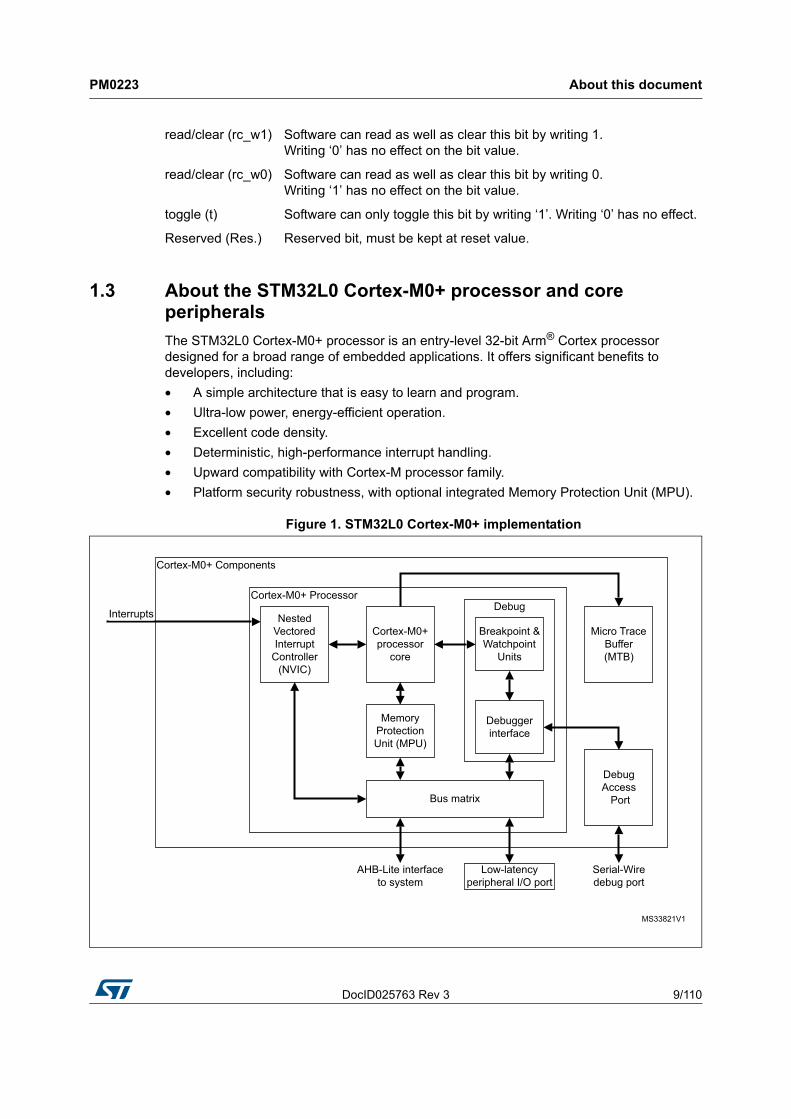
Figure 1. STM32L0 Cortex-M0+ implementation
read/clear (rc_w1) Software can read as well as clear this bit by writing 1. Writing ‘0’ has no effect on the bit value.
read/clear (rc_w0) Software can read as well as clear this bit by writing 0. Writing ‘1’ has no effect on the bit value.
toggle (t) Software can only toggle this bit by writing ‘1’. Writing ‘0’ has no effect.
Reserved (Res.) Reserved bit, must be kept at reset value.
About this document PM0223
10/110 DocID025763 Rev 3
The STM32L0 Cortex-M0+ processor is built on a highly area and power optimized 32-bit processor core, with a 2-stage pipeline Von Neumann architecture. The processor delivers exceptional energy efficiency through a small but powerful instruction set and extensively optimized design, providing high-end processing hardware including a single-cycle multiplier.
The STM32L0 Cortex-M0+ processor implements the ARMv6-M architecture, which is based on the 16-bit Thumb
® instruction set and includes Thumb-2 technology. This provides
the exceptional performance expected of a modern 32-bit architecture, with a higher code density than other 8-bit and 16-bit microcontrollers.
The STM32L0 Cortex-M0+ processor closely integrates a configurable Nested vectored interrupt controller (NVIC), to deliver industry-leading interrupt performance. The NVIC:
• Includes a Non-Maskable Interrupt (NMI).
• Provides zero jitter interrupt option.
• Provides four interrupt priority levels.
The tight integration of the processor core and NVIC provides fast execution of Interrupt Service Routines (ISRs), dramatically reducing the interrupt latency. This is achieved through the hardware stacking of registers, and the ability to abandon and restart load-multiple and store-multiple operations. Interrupt handlers do not require any assembler wrapper code, removing any code overhead from the ISRs. Tail-chaining optimization also significantly reduces the overhead when switching from one ISR to another.
To optimize low-power designs, the NVIC integrates with the sleep modes, that include a deep sleep function that enables the entire device to be rapidly powered down.
1.3.1 System-level interface
The STM32L0 Cortex-M0+ processor provides a single system-level interface using AMBA®
technology to provide high speed, low latency memory accesses.
The STM32L0 Cortex-M0+ processor has an optional Memory Protection Unit (MPU) that provides fine grain memory control, enabling applications to use multiple privilege levels, separating and protecting code, data and stack on a task-by-task basis. Such requirements are becoming critical in many embedded applications such as automotive systems.
1.3.2 Integrated configurable debug
The STM32L0 Cortex-M0+ processor implements a complete hardware debug solution, with extensive hardware breakpoint and watchpoint options. This provides high system visibility of the processor, memory and peripherals through a <2-pin Serial Wire Debug (SWD) port> that is ideal for microcontrollers and other small package devices.
DocID025763 Rev 3 11/110
PM0223 About this document
35
1.3.3 STM32L0 Cortex-M0+ processor features summary
• Thumb instruction set with Thumb-2 Technology.
• High code density with 32-bit performance.
• User and Privileged mode execution.
• Tools and binary upwards compatible with Cortex-M processor family.
• Integrated ultra low-power sleep modes.
• Efficient code execution enabling slower processor clock or increased sleep time.
• Single-cycle 32-bit hardware multiplier.
• Zero jitter interrupt handling.
• Memory Protection Unit (MPU) for safety-critical applications.
• Low latency, high-speed peripheral I/O port.
• A Vector Table Offset Register.
• Extensive debug capabilities.
1.3.4 STM32L0 Cortex-M0+ core peripherals
These are:
Nested vectored interrupt controller (NVIC)
The NVIC is an embedded interrupt controller that supports low latency interrupt processing.
System Control Block
The System Control Block (SCB) is the programmers model interface to the processor. It provides system implementation information and system control, including configuration, control, and reporting of system exceptions.
System timer
The system timer, SysTick, is a 24-bit count-down timer. Use this as a Real Time Operating System (RTOS) tick timer or as a simple counter.
Memory Protection Unit
The Memory Protection Unit (MPU) improves system reliability by defining the memory attributes for different memory regions. It provides up to eight different regions, and an optional predefined background region.
I/O port
The I/O port provides single-cycle loads and stores to tightly-coupled peripherals.
The STM32L0 Cortex-M0+ Processor PM0223
12/110 DocID025763 Rev 3
2 The STM32L0 Cortex-M0+ Processor
2.1 Programmers model
This section describes the STM32L0 Cortex-M0+ programmers model. In addition to the individual core register descriptions, it contains information about the processor modes, privilege levels for software execution, and stacks.
2.1.1 Processor modes and privilege levels for software execution
The processor modes are:
The privilege levels for software execution are:
In Thread mode, the CONTROL register controls whether software execution is privileged or unprivileged, see CONTROL register on page 18. In Handler mode, software execution is always privileged.
Only privileged software can write to the CONTROL register to change the privilege level for software execution in Thread mode. Unprivileged software can use the SVC instruction to make a Supervisor Call to transfer control to privileged software.
2.1.2 Stacks
The processor uses a full descending stack. This means the stack pointer indicates the last stacked item on the stack memory. When the processor pushes a new item onto the stack, it decrements the stack pointer and then writes the item to the new memory location. The processor implements two stacks, the main stack and the process stack, with independent copies of the stack pointer, see Stack Pointer on page 14.
In Thread mode, the CONTROL register controls whether the processor uses the main stack or the process stack, see CONTROL register on page 18. In Handler mode, the processor always uses the main stack. The options for processor operations are:
Thread mode Executes application software. The processor enters Thread mode when it comes out of reset.
Handler mode Handles exceptions. The processor returns to Thread mode when it has finished all exception processing.
Unprivileged The software:
• Has limited access to system registers using the MSR and MRS instructions, and cannot use the CPS instruction to mask interrupts.
• Cannot access the system timer, NVIC, or system control block.
• Might have restricted access to memory or peripherals.
Unprivileged software executes at the unprivileged level.
Privileged The software can use all the instructions and has access to all resources.
Privileged software executes at the privileged level.
DocID025763 Rev 3 13/110
PM0223 The STM32L0 Cortex-M0+ Processor
35
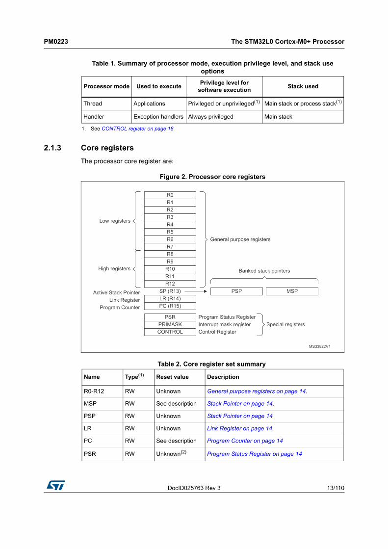
2.1.3 Core registers
The processor core register are:
Figure 2. Processor core registers
Table 1. Summary of processor mode, execution privilege level, and stack use options
Processor mode Used to executePrivilege level for
software executionStack used
Thread Applications Privileged or unprivileged(1)
1. See CONTROL register on page 18
Main stack or process stack(1)
Handler Exception handlers Always privileged Main stack
Table 2. Core register set summary
Name Type(1) Reset value Description
R0-R12 RW Unknown General purpose registers on page 14.
MSP RW See description Stack Pointer on page 14.
PSP RW Unknown Stack Pointer on page 14
LR RW Unknown Link Register on page 14
PC RW See description Program Counter on page 14
PSR RW Unknown(2) Program Status Register on page 14
The STM32L0 Cortex-M0+ Processor PM0223
14/110 DocID025763 Rev 3
General purpose registers
R0-R12 are 32-bit general purpose registers for data operations.
Stack Pointer
The Stack Pointer (SP) is register R13. In Thread mode, bit[1] of the CONTROL register indicates the stack pointer to use:
• 0 = Main Stack Pointer (MSP). This is the reset value.
• 1 = Process Stack Pointer (PSP).
On reset, the processor loads the MSP with the value from address 0x00000000.
Link Register
The Link Register (LR) is register R14. It stores the return information for subroutines, function calls, and exceptions. On reset, the LR value is Unknown.
Program Counter
The Program Counter (PC) is register R15. It contains the current program address. On reset, the processor loads the PC with the value of the reset vector, which is at address 0x00000004. Bit[0] of the value is loaded into the EPSR T-bit at reset and must be 1.
Program Status Register
The Program Status Register (PSR) combines:
• Application Program Status Register (APSR).
• Interrupt Program Status Register (IPSR).
• Execution Program Status Register (EPSR).
These registers are allocated as mutually exclusive bitfields within the 32-bit PSR. The PSR bit assignments are:
APSR RW Unknown Application Program Status Register on page 15
IPSR RO 0x00000000 Interrupt Program Status Register on page 16
EPSR RO Unknown Execution Program Status Register on page 16
PRIMASK RW 0x00000000 Priority Mask Register on page 17
CONTROL RW 0x00000000 CONTROL register on page 18
1. Describes access type during program execution in Thread mode and Handler mode. Debug access can differ.
2. Bit[24] is the T-bit and is loaded from bit[0] of the reset vector.
Table 2. Core register set summary (continued)
DocID025763 Rev 3 15/110
PM0223 The STM32L0 Cortex-M0+ Processor
35
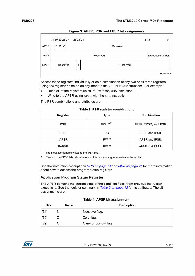
Figure 3. APSR, IPSR and EPSR bit assignments
Access these registers individually or as a combination of any two or all three registers, using the register name as an argument to the MSR or MRS instructions. For example:
• Read all of the registers using PSR with the MRS instruction.
• Write to the APSR using APSR with the MSR instruction.
The PSR combinations and attributes are:
See the instruction descriptions MRS on page 74 and MSR on page 75 for more information about how to access the program status registers.
Application Program Status Register
The APSR contains the current state of the condition flags, from previous instruction executions. See the register summary in Table 2 on page 13 for its attributes. The bit assignments are:
Table 3. PSR register combinations
Register Type Combination
PSR RW(1),(2)
1. The processor ignores writes to the IPSR bits.
2. Reads of the EPSR bits return zero, and the processor ignores writes to these bits.
APSR, EPSR, and IPSR.
IEPSR RO EPSR and IPSR.
IAPSR RW(1) APSR and IPSR.
EAPSR RW(2) APSR and EPSR.
Table 4. APSR bit assignment
Bits Name Description
[31] N Negative flag.
[30] Z Zero flag.
[29] C Carry or borrow flag.
The STM32L0 Cortex-M0+ Processor PM0223
16/110 DocID025763 Rev 3
See The condition flags on page 43 for more information about the APSR negative, zero, carry or borrow, and overflow flags.
Interrupt Program Status Register
The IPSR contains the exception number of the current Interrupt Service Routine (ISR). See the register summary in Table 2 on page 13 for its attributes. The bit assignments are:
Execution Program Status Register
The EPSR contains the Thumb state bit.
See the register summary in Table 2 on page 13 for the EPSR attributes. The bit assignments are:
[28] V Overflow flag.
[27:0] - Reserved.
Table 5. IPSR bit assignments
Bits Name Function
[31:6] - Reserved
[5:0] Exception number This is the number of the current exception:
0 = Thread mode.
1 = Reserved.
2 = NMI.
3 = HardFault.
4-10 = Reserved.
11 = SVCall.
12, 13 = Reserved.
14 = PendSV.
15 = SysTick | Reserved.
16 = IRQ0.
.
.
47 = IRQ31.
48-63 = Reserved.
see Exception types on page 26 for more information.
Table 4. APSR bit assignment (continued)
Bits Name Description
DocID025763 Rev 3 17/110
PM0223 The STM32L0 Cortex-M0+ Processor
35
Attempts by application software to read the EPSR directly using the MRS instruction always return zero. Attempts to write the EPSR using the MRS instruction are ignored. Fault handlers can examine the EPSR value in the stacked PSR to determine the cause of the fault. See Exception entry and return on page 30. The following can clear the T bit to 0:
• Instructions BLX, BX and POP{PC}.
• Restoration from the stacked xPSR value on an exception return.
• Bit[0] of the vector value on an exception entry.
Attempting to execute instructions when the T bit is 0 results in a HardFault or Lockup. See 2.4.1: Lockup on page 33 for more information.
Interruptible-restartable instructions
The interruptible-restartable instructions are LDM and STM, PUSH, POP, and MULS. When an interrupt occurs during the execution of one of these instructions, the processor abandons execution of the instruction. After servicing the interrupt, the processor restarts execution of the instruction from the beginning.
Exception mask register
The exception mask register disables the handling of exceptions by the processor. Disable exceptions where they might impact on timing critical tasks or code sequences requiring atomicity.
To disable or re-enable exceptions, use the MSR and MRS instructions, or the CPS instruction, to change the value of PRIMASK. 3.7.6: MRS on page 74, 3.7.7: MSR on page 75, and 3.7.2: CPS on page 70 for more information.
Priority Mask Register
The PRIMASK register prevents activation of all exceptions with configurable priority. See the register summary in Table 2 on page 13 for its attributes. The bit assignments are:
Table 6. EPSR bit assignments
Bits Name Function
[31:25] - Reserved.
[24] T Thumb state bit.
[23:0] - Reserved.
Table 7. PRIMASK register bit assignments
Bits Name Function
[31:1] - Reserved.
[0] PM Prioritizable interrupt mask:
0 = No effect.
1 = Prevents the activation of all exceptions with configurable priority.
The STM32L0 Cortex-M0+ Processor PM0223
18/110 DocID025763 Rev 3
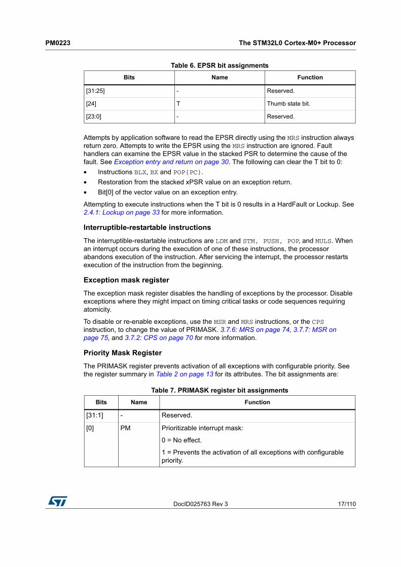
CONTROL register
The CONTROL register controls the stack used, and the privilege level for software execution, when the processor is in Thread mode. See the register summary in Table 2 on page 13 for its attributes. The bit assignments are:
Figure 4. Control bit assignment
Handler mode always uses the MSP, so the processor ignores explicit writes to the active stack pointer bit of the CONTROL register when in Handler mode. The exception entry and return mechanisms automatically update the CONTROL register.
In an OS environment, it is recommended that threads running in Thread mode use the process stack and the kernel and exception handlers use the main stack.
By default, Thread mode uses the MSP. To switch the stack pointer used in Thread mode to the PSP, use the MSR instruction to set the active stack pointer bit to 1, 3.7.6: MRS on page 74
Note: When changing the stack pointer, software must use an ISB instruction immediately after the MSR instruction. This ensures that instructions after the ISB execute using the new stack pointer. See 3.7.5: ISB on page 73.
2.1.4 Exceptions and interrupts
The STM32L0 Cortex-M0+ processor supports interrupts and system exceptions. The processor and the Nested vectored interrupt controller (NVIC) prioritize and handle all exceptions. An interrupt or exception changes the normal flow of software control. The processor uses Handler mode to handle all exceptions except for reset. See Exception entry
Table 8. Control register bit assignments
Bits Name Function
[31:2] - Reserved.
[1] SPSEL
Defines the current stack:
0 = MSP is the current stack pointer.
1 = PSP is the current stack pointer.
In Handler mode this bit reads as zero and ignores writes.
[0] nPRIV
Defines the Thread mode privilege level:
0 = Privileged.
1 = Unprivileged.
DocID025763 Rev 3 19/110
PM0223 The STM32L0 Cortex-M0+ Processor
35
on page 31 and Exception return on page 32 for more information.
The NVIC registers control interrupt handling. See 4.2: Nested vectored interrupt controller on page 82 for more information.
2.1.5 Data types
The processor:
• Supports the following data types:
– 32-bit words.
– 16-bit halfwords.
– 8-bit bytes.
• Manages all data memory accesses as little-endian or big-endian. Instruction memory and Private Peripheral Bus (PPB) accesses are always little-endian. See 2.2.1: Memory regions, types and attributes on page 21 for more information.
2.1.6 The Cortex Microcontroller Software Interface Standard
Arm® provides the Cortex Microcontroller Software Interface Standard (CMSIS) for programming STM32L0 Cortex-M0+ microcontrollers. The CMSIS is an integrated part of the device driver library. For a STM32L0 Cortex-M0+ microcontroller system, CMSIS defines:
• A common way to:
– Access peripheral registers.
– Define exception vectors.
• The names of:
– The registers of the core peripherals.
– The core exception vectors.
• A device-independent interface for RTOS kernels.
The CMSIS includes address definitions and data structures for the core peripherals in the STM32L0 Cortex-M0+ processor. It also includes optional interfaces for middleware components comprising a TCP/IP stack and a Flash file system.
The CMSIS simplifies software development by enabling the reuse of template code, and the combination of CMSIS-compliant software components from various middleware vendors. Software vendors can expand the CMSIS to include their peripheral definitions and access functions for those peripherals.
This document includes the register names defined by the CMSIS, and gives short descriptions of the CMSIS functions that address the processor core and the core peripherals.
Note: This document uses the register short names defined by the CMSIS. In a few cases these differ from the architectural short names that might be used in other documents.
The STM32L0 Cortex-M0+ Processor PM0223
20/110 DocID025763 Rev 3
The following sections give more information about the CMSIS:
• 2.5.4: Power management programming hints on page 35
• 3.2: Intrinsic functions on page 39
• 4.2.1: Accessing the STM32L0 Cortex-M0+ NVIC registers using CMSIS on page 82
• NVIC programming hints on page 87
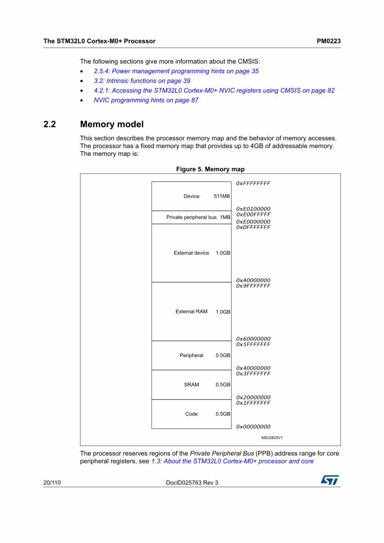
2.2 Memory model
This section describes the processor memory map and the behavior of memory accesses. The processor has a fixed memory map that provides up to 4GB of addressable memory. The memory map is:
Figure 5. Memory map
The processor reserves regions of the Private Peripheral Bus (PPB) address range for core peripheral registers, see 1.3: About the STM32L0 Cortex-M0+ processor and core
DocID025763 Rev 3 21/110
PM0223 The STM32L0 Cortex-M0+ Processor
35
peripherals on page 9.
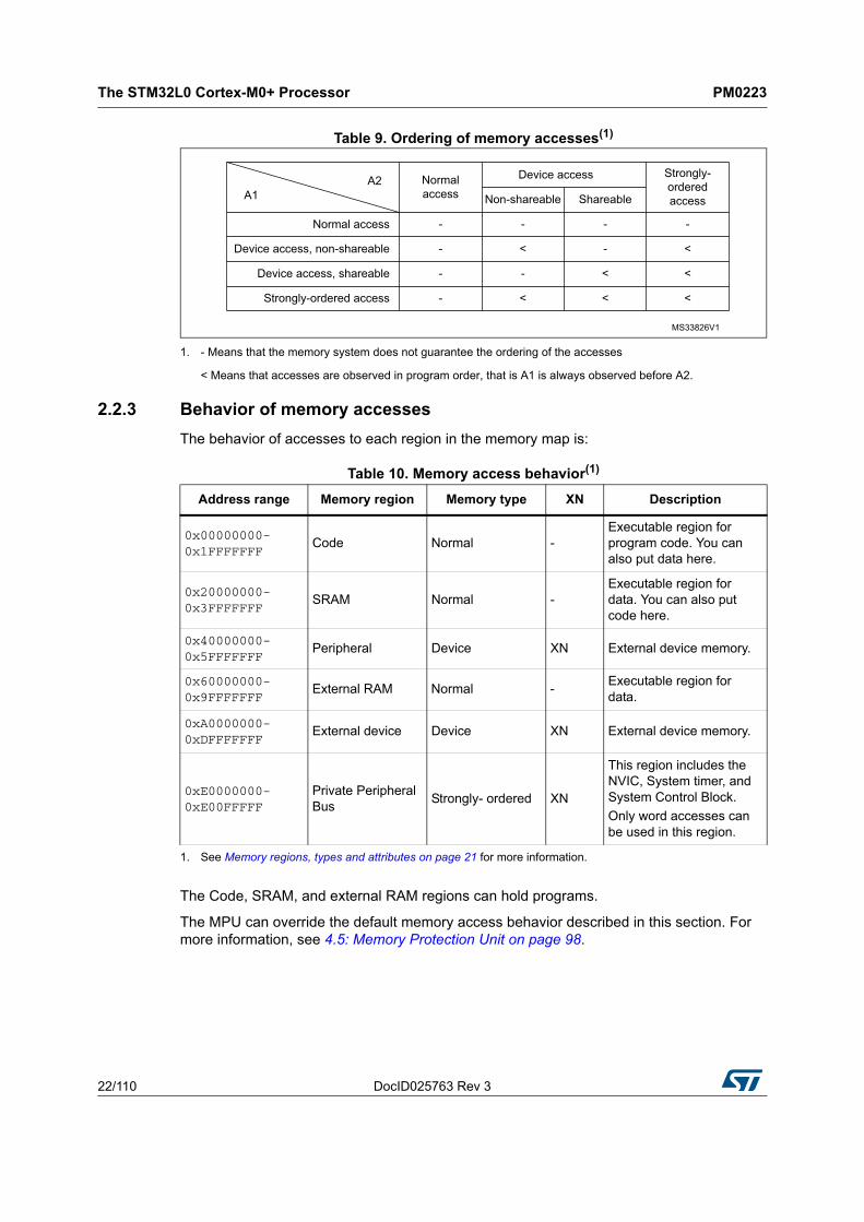
2.2.1 Memory regions, types and attributes
The memory map and the programming of the MPU splits into regions. Each region has a defined memory type, and some regions have additional memory attributes. The memory type and attributes determine the behavior of accesses to the region.
The memory types are:
The different ordering requirements for Device and Strongly-ordered memory mean that the memory system can buffer a write to Device memory, but must not buffer a write to Strongly-ordered memory.
The additional memory attributes include.
2.2.2 Memory system ordering of memory accesses
For most memory accesses caused by explicit memory access instructions, the memory system does not guarantee that the order in which the accesses complete matches the program order of the instructions, providing any re-ordering does not affect the behavior of the instruction sequence. Normally, if correct program execution depends on two memory accesses completing in program order, software must insert a memory barrier instruction between the memory access instructions, see 2.2.2: Memory system ordering of memory accesses on page 21.
However, the memory system does guarantee some ordering of accesses to Device and Strongly-ordered memory. For two memory access instructions A1 and A2, if A1 occurs before A2 in program order, the ordering of the memory accesses caused by two instructions is:
Normal The processor can re-order transactions for efficiency, or perform speculative reads.
Device The processor preserves transaction order relative to other transactions to Device or Strongly-ordered memory.
Strongly-ordered The processor preserves transaction order relative to all other transactions.
Shareable For a shareable memory region, the memory system provides data synchronization between bus masters in a system with multiple bus masters, for example, a processor with a DMA controller.
Strongly-ordered memory is always shareable.
If multiple bus masters can access a non-shareable memory region, software must ensure data coherency between the bus masters.
<This description is required only if the device is likely to be used in systems where memory is shared between multiple processors.>
Execute Never (XN) Means the processor prevents instruction accesses. A HardFault exception is generated on executing an instruction fetched from an XN region of memory.
The STM32L0 Cortex-M0+ Processor PM0223
22/110 DocID025763 Rev 3
Table 9. Ordering of memory accesses(1)
1. - Means that the memory system does not guarantee the ordering of the accesses < Means that accesses are observed in program order, that is A1 is always observed before A2.
2.2.3 Behavior of memory accesses
The behavior of accesses to each region in the memory map is:
The Code, SRAM, and external RAM regions can hold programs.
The MPU can override the default memory access behavior described in this section. For more information, see 4.5: Memory Protection Unit on page 98.
Table 10. Memory access behavior(1)
1. See Memory regions, types and attributes on page 21 for more information.
Address range Memory region Memory type XN Description
0x00000000- 0x1FFFFFFF
Code Normal -Executable region for program code. You can also put data here.
0x20000000- 0x3FFFFFFF
SRAM Normal -Executable region for data. You can also put code here.
0x40000000- 0x5FFFFFFF
Peripheral Device XN External device memory.
0x60000000- 0x9FFFFFFF
External RAM Normal -Executable region for data.
0xA0000000- 0xDFFFFFFF
External device Device XN External device memory.
0xE0000000- 0xE00FFFFF
Private Peripheral Bus
Strongly- ordered XN
This region includes the NVIC, System timer, and System Control Block.
Only word accesses can be used in this region.
DocID025763 Rev 3 23/110
PM0223 The STM32L0 Cortex-M0+ Processor
35
2.2.4 Additional memory access constraints for caches and shared memory
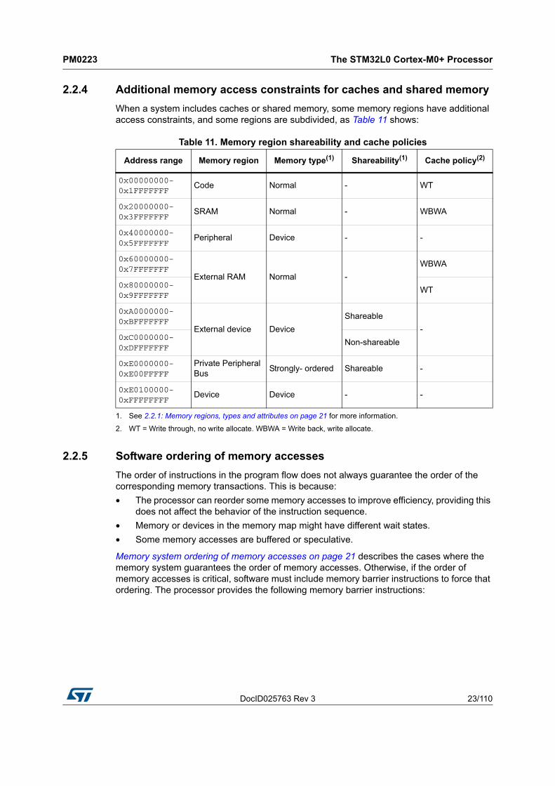
When a system includes caches or shared memory, some memory regions have additional access constraints, and some regions are subdivided, as Table 11 shows:
2.2.5 Software ordering of memory accesses
The order of instructions in the program flow does not always guarantee the order of the corresponding memory transactions. This is because:
• The processor can reorder some memory accesses to improve efficiency, providing this does not affect the behavior of the instruction sequence.
• Memory or devices in the memory map might have different wait states.
• Some memory accesses are buffered or speculative.
Memory system ordering of memory accesses on page 21 describes the cases where the memory system guarantees the order of memory accesses. Otherwise, if the order of memory accesses is critical, software must include memory barrier instructions to force that ordering. The processor provides the following memory barrier instructions:
Table 11. Memory region shareability and cache policies
Address range Memory region Memory type(1)
1. See 2.2.1: Memory regions, types and attributes on page 21 for more information.
Shareability(1) Cache policy(2)
2. WT = Write through, no write allocate. WBWA = Write back, write allocate.
0x00000000- 0x1FFFFFFF
Code Normal - WT
0x20000000- 0x3FFFFFFF
SRAM Normal - WBWA
0x40000000- 0x5FFFFFFF
Peripheral Device - -
0x60000000- 0x7FFFFFFF
External RAM Normal -
WBWA
0x80000000- 0x9FFFFFFF
WT
0xA0000000- 0xBFFFFFFF
External device Device
Shareable
-0xC0000000- 0xDFFFFFFF
Non-shareable
0xE0000000- 0xE00FFFFF
Private Peripheral Bus
Strongly- ordered Shareable -
0xE0100000- 0xFFFFFFFF
Device Device - -
The STM32L0 Cortex-M0+ Processor PM0223
24/110 DocID025763 Rev 3
The following are examples of using memory barrier instructions:
Memory accesses to Strongly-ordered memory, such as the System Control Block, do not require the use of DMB instructions.
2.2.6 Memory endianness
The processor views memory as a linear collection of bytes numbered in ascending order from zero. For example, bytes 0-3 hold the first stored word, and bytes 4-7 hold the second stored word. Little-endian format describes how words of data are stored in memory.
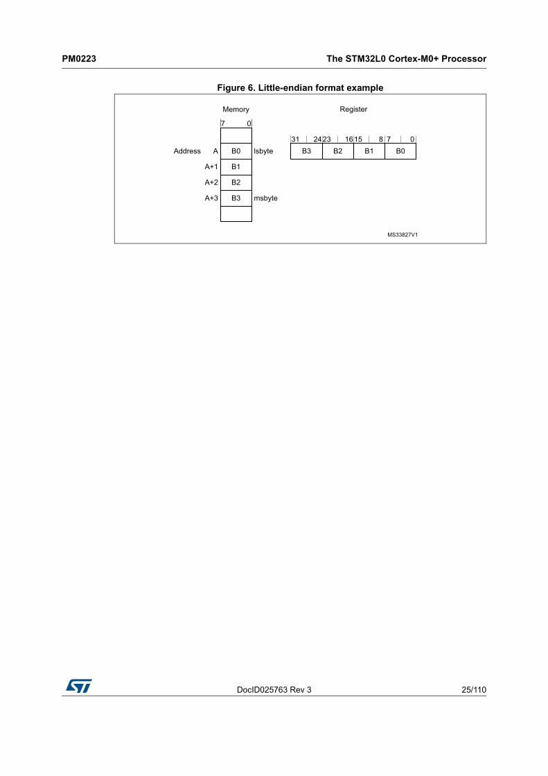
Little-endian format
In little-endian format, the processor stores the least significant byte (lsbyte) of a word at the lowest-numbered byte, and the most significant byte (msbyte) at the highest-numbered byte. For example:
DMB The Data Memory Barrier (DMB) instruction ensures that outstanding memory transactions complete before subsequent memory transactions. See DMB on page 71.
DSB The Data Synchronization Barrier (DSB) instruction ensures that outstanding memory transactions complete before subsequent instructions execute. See DSB on page 72.
ISB The Instruction Synchronization Barrier (ISB) ensures that the effect of all completed memory transactions is recognizable by subsequent instructions. See ISB on page 73.
Vector table If the program changes an entry in the vector table, and then enables the corresponding exception, use a DMB instruction between the operations. This ensures that if the exception is taken immediately after being enabled the processor uses the new exception vector.
Self-modifying code If a program contains self-modifying code, use an ISB instruction immediately after the code modification in the program. This ensures subsequent instruction execution uses the updated program.
Memory map switching If the system contains a memory map switching mechanism, use a DSB instruction after switching the memory map. This ensures subsequent instruction execution uses the updated memory map
MPU programming Use a DSB followed by an ISB instruction or exception return to ensure that the new MPU configuration is used by subsequent instructions.
VTOR programming If the program updates the value of the VTOR, use a DMB instruction to ensure that the new vector table is used for subsequent exceptions.
DocID025763 Rev 3 25/110
PM0223 The STM32L0 Cortex-M0+ Processor
35
Figure 6. Little-endian format example
The STM32L0 Cortex-M0+ Processor PM0223
26/110 DocID025763 Rev 3
2.3 Exception model
This section describes the exception model.
2.3.1 Exception states
Each exception is in one of the following states:
2.3.2 Exception types
The exception types are:
Inactive The exception is not active and not pending.
Pending The exception is waiting to be serviced by the processor.
An interrupt request from a peripheral or from software can change the state of the corresponding interrupt to pending.
Active An exception that is being serviced by the processor but has not completed.Note: An exception handler can interrupt the execution of another exception
handler. In this case both exceptions are in the active state.
Active and pendingThe exception is being serviced by the processor and there is a pending exception from the same source.
Reset Reset is invoked on power up or a warm reset. The exception model treats reset as a special form of exception. When reset is asserted, the operation of the processor stops, potentially at any point in an instruction. When reset is deasserted, execution restarts from the address provided by the reset entry in the vector table. Execution restarts as privileged execution in Thread mode.
NMI A NonMaskable Interrupt (NMI) can be signalled by a peripheral or triggered by software. This is the highest priority exception other than reset. It is permanently enabled and has a fixed priority of -2. NMIs cannot be:
• Masked or prevented from activation by any other exception.
• Preempted by any exception other than Reset.
HardFault A HardFault is an exception that occurs because of an error during normal or exception processing. HardFaults have a fixed priority of -1, meaning they have higher priority than any exception with configurable priority.
SVCall A Supervisor Call (SVC) is an exception that is triggered by the SVC instruction. In an OS environment, applications can use SVC instructions to access OS kernel functions and device drivers.
PendSV PendSV is an interrupt-driven request for system-level service. In an OS environment, use PendSV for context switching when no other exception is active.
DocID025763 Rev 3 27/110
PM0223 The STM32L0 Cortex-M0+ Processor
35
For an asynchronous exception, other than reset, the processor can execute additional instructions between when the exception is triggered and when the processor enters the exception handler.
Privileged software can disable the exceptions that Table 12 on page 27 shows as having configurable priority, see 4.2.3: Interrupt Clear-enable Register on page 83.
For more information about HardFaults, see 2.4: Fault handling on page 33
SysTick A SysTick exception is an exception the system timer generates when it reaches zero. Software can also generate a SysTick exception. In an OS environment, the processor can use this exception as system tick.
Interrupt (IRQ) An interrupt, or IRQ, is an exception signalled by a peripheral, or generated by a software request. All interrupts are asynchronous to instruction execution. In the system, peripherals use interrupts to communicate with the processor.
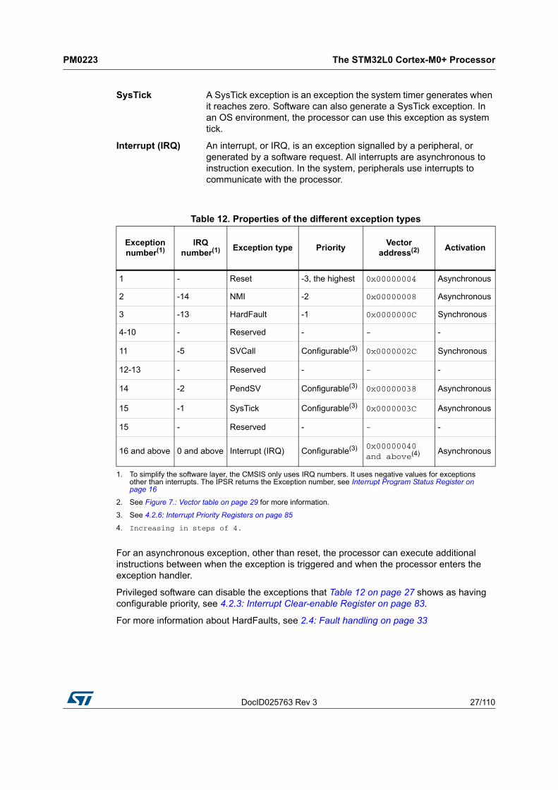
Table 12. Properties of the different exception types
Exception number(1)
1. To simplify the software layer, the CMSIS only uses IRQ numbers. It uses negative values for exceptions other than interrupts. The IPSR returns the Exception number, see Interrupt Program Status Register on page 16
IRQnumber(1) Exception type Priority
Vector address(2)
2. See Figure 7.: Vector table on page 29 for more information.
Activation
1 - Reset -3, the highest 0x00000004 Asynchronous
2 -14 NMI -2 0x00000008 Asynchronous
3 -13 HardFault -1 0x0000000C Synchronous
4-10 - Reserved - - -
11 -5 SVCall Configurable(3)
3. See 4.2.6: Interrupt Priority Registers on page 85
0x0000002C Synchronous
12-13 - Reserved - - -
14 -2 PendSV Configurable(3) 0x00000038 Asynchronous
15 -1 SysTick Configurable(3) 0x0000003C Asynchronous
15 - Reserved - - -
16 and above 0 and above Interrupt (IRQ) Configurable(3) 0x00000040 and above(4)
4. Increasing in steps of 4.
Asynchronous
The STM32L0 Cortex-M0+ Processor PM0223
28/110 DocID025763 Rev 3
2.3.3 Exception handlers
The processor handles exceptions using:
Interrupt Service Routines (ISRs) Interrupts IRQ0 to IRQ31 are the exceptions handled by ISRs
Fault handler HardFault is the only exception handled by the fault handler.
System handlers NMI, PendSV, SVCall SysTick, and HardFault are all system exceptions handled by system handlers.
DocID025763 Rev 3 29/110
PM0223 The STM32L0 Cortex-M0+ Processor
35
2.3.4 Vector table
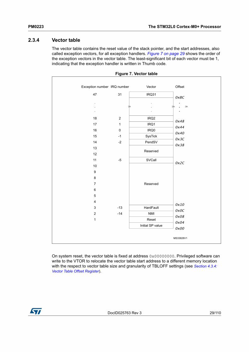
The vector table contains the reset value of the stack pointer, and the start addresses, also called exception vectors, for all exception handlers. Figure 7 on page 29 shows the order of the exception vectors in the vector table. The least-significant bit of each vector must be 1, indicating that the exception handler is written in Thumb code.
Figure 7. Vector table
On system reset, the vector table is fixed at address 0x00000000. Privileged software can write to the VTOR to relocate the vector table start address to a different memory location with the respect to vector table size and granularity of TBLOFF settings (see Section 4.3.4: Vector Table Offset Register).
The STM32L0 Cortex-M0+ Processor PM0223
30/110 DocID025763 Rev 3
2.3.5 Exception priorities
As Table 12 on page 27 shows, all exceptions have an associated priority, with:
• A lower priority value indicating a higher priority.
• Configurable priorities for all exceptions except Reset, HardFault, and NMI.
If software does not configure any priorities, then all exceptions with a configurable priority have a priority of 0. For information about configuring exception priorities see
• 4.3.8: System Handler Priority Registers on page 94
• I4.2.6: Interrupt Priority Registers on page 85.
Note: Configurable priority values are in the range 0-192, in steps of 64. The Reset, HardFault, and NMI exceptions, with fixed negative priority values, always have higher priority than any other exception.
Assigning a higher priority value to IRQ[0] and a lower priority value to IRQ[1] means that IRQ[1] has higher priority than IRQ[0]. If both IRQ[1] and IRQ[0] are asserted, IRQ[1] is processed before IRQ[0].
If multiple pending exceptions have the same priority, the pending exception with the lowest exception number takes precedence. For example, if both IRQ[0] and IRQ[1] are pending and have the same priority, then IRQ[0] is processed before IRQ[1].
When the processor is executing an exception handler, the exception handler is preempted if a higher priority exception occurs. If an exception occurs with the same priority as the exception being handled, the handler is not preempted, irrespective of the exception number. However, the status of the new interrupt changes to pending.
2.3.6 Exception entry and return
Descriptions of exception handling use the following terms:
Preemption When the processor is executing an exception handler, an exception can preempt the exception handler if its priority is higher than the priority of the exception being handled.
When one exception preempts another, the exceptions are called nested exceptions. See Exception entry on page 31 for more information.
Return This occurs when the exception handler is completed, and:
• There is no pending exception with sufficient priority to be serviced.
• The completed exception handler was not handling a late-arriving exception.
The processor pops the stack and restores the processor state to the state it had before the interrupt occurred. See Exception return on page 32 for more information.
DocID025763 Rev 3 31/110
PM0223 The STM32L0 Cortex-M0+ Processor
35
Exception entry
Exception entry occurs when there is a pending exception with sufficient priority and either:
• The processor is in Thread mode.
• The new exception is of higher priority than the exception being handled, in which case the new exception preempts the exception being handled.
When one exception preempts another, the exceptions are nested.
Sufficient priority means the exception has greater priority than any limit set by the mask register, see Exception mask register on page 17. An exception with less priority than this is pending but is not handled by the processor.
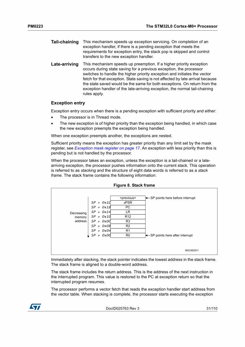
When the processor takes an exception, unless the exception is a tail-chained or a late-arriving exception, the processor pushes information onto the current stack. This operation is referred to as stacking and the structure of eight data words is referred to as a stack frame. The stack frame contains the following information:
Figure 8. Stack frame
Immediately after stacking, the stack pointer indicates the lowest address in the stack frame. The stack frame is aligned to a double-word address.
The stack frame includes the return address. This is the address of the next instruction in the interrupted program. This value is restored to the PC at exception return so that the interrupted program resumes.
The processor performs a vector fetch that reads the exception handler start address from the vector table. When stacking is complete, the processor starts executing the exception
Tail-chaining This mechanism speeds up exception servicing. On completion of an exception handler, if there is a pending exception that meets the requirements for exception entry, the stack pop is skipped and control transfers to the new exception handler.
Late-arriving This mechanism speeds up preemption. If a higher priority exception occurs during state saving for a previous exception, the processor switches to handle the higher priority exception and initiates the vector fetch for that exception. State saving is not affected by late arrival because the state saved would be the same for both exceptions. On return from the exception handler of the late-arriving exception, the normal tail-chaining rules apply.
The STM32L0 Cortex-M0+ Processor PM0223
32/110 DocID025763 Rev 3
handler. At the same time, the processor writes an EXC_RETURN value to the LR. This indicates which stack pointer corresponds to the stack frame and what operation mode the processor was in before the entry occurred.
If no higher priority exception occurs during exception entry, the processor starts executing the exception handler and automatically changes the status of the corresponding pending interrupt to active.
If another higher priority exception occurs during exception entry, the processor starts executing the exception handler for this exception and does not change the pending status of the earlier exception. This is the late arrival case.
Exception return
Exception return occurs when the processor is in Handler mode and execution of one of the following instructions attempts to set the PC to an EXC_RETURN value:
• A POP instruction that loads the PC.
• B PBX instruction using any register.
The processor saves an EXC_RETURN value to the LR on exception entry. The exception mechanism relies on this value to detect when the processor has completed an exception handler. Bits[31:4] of an EXC_RETURN value are 0xFFFFFFF. When the processor loads a value matching this pattern to the PC it detects that the operation is a not a normal branch operation and, instead, that the exception is complete. As a result, it starts the exception return sequence. Bits[3:0] of the EXC_RETURN value indicate the required return stack and processor mode, as Table 13 on page 32 shows.
Table 13. Exception return behavior
EXC_RETURN Description
0xFFFFFF1
Return to Handler mode.
Exception return gets state from the main stack.
Execution uses MSP after return.
0xFFFFFF9
Return to Thread mode.
Exception return gets state from MSP.
Execution uses MSP after return.
0xFFFFFFD
Return to Thread mode.
Exception return gets state from PSP.
Execution uses PSP after return.
All other values Reserved.
DocID025763 Rev 3 33/110
PM0223 The STM32L0 Cortex-M0+ Processor
35
2.4 Fault handling
Faults are a subset of exceptions, see 2.3: Exception model on page 26. All faults result in the HardFault exception being taken or cause Lockup if they occur in the NMI or HardFault handler. The faults are:
• Execution of an SVC instruction at a priority equal or higher than SVCall.
• Execution of a BKPT instruction without a debugger attached.
• A system-generated bus error on a load or store.
• Execution of an instruction from an XN memory address.
• Execution of an instruction from a location for which the system generates a bus fault.
• A system-generated bus error on a vector fetch.
• Execution of an Undefined instruction.
• Execution of an instruction when not in Thumb state as a result of the T-bit being previously cleared to 0.
• An attempted load or store to an unaligned address.
• An MPU fault because of a privilege violation or an attempt to access an unmanaged region.
Note: Only Reset and NMI can preempt the fixed priority HardFault handler. A HardFault can preempt any exception other than Reset, NMI, or another HardFault.
2.4.1 Lockup
The processor enters a Lockup state if a fault occurs when executing the NMI or HardFault handlers, or if the system generates a bus error when unstacking the PSR on an exception return using the MSP. When the processor is in Lockup state it does not execute any instructions. The processor remains in Lockup state until one of the following occurs:
• It is reset.
• A debugger halts it.
• An NMI occurs and the current Lockup is in the HardFault handler.
Note: If Lockup state occurs in the NMI handler a subsequent NMI does not cause the processor to leave Lockup state.
2.5 Power management
The STM32L0 Cortex-M0+ processor sleep modes reduce power consumption:
• A sleep mode, that stops the processor clock.
• A deep sleep mode, that enters ultra low-power modes.
The SLEEPDEEP bit of the SCR selects which sleep mode is used, see 4.3.6: System Control Register on page 92. When entering the deep sleep mode, the PDSS bit in
The STM32L0 Cortex-M0+ Processor PM0223
34/110 DocID025763 Rev 3
PWR_CR register will select entry in Stop or Standby mode, see the reference manual chapter "low-power modes" for details.
This section describes the mechanisms for entering sleep mode, and the conditions for waking up from sleep mode.
2.5.1 Entering sleep mode
This section describes the mechanisms software can use to put the processor into sleep mode.
The system can generate spurious wakeup events, for example a debug operation wakes up the processor. For this reason, software must be able to put the processor back into sleep mode after such an event. A program might have an idle loop to put the processor back in to sleep mode.
Wait for interrupt
The Wait For Interrupt instruction, WFI, causes immediate entry to sleep mode. When the processor executes a WFI instruction it stops executing instructions and enters sleep mode. See 3.7.12: WFI on page 80 for more information.
Wait for event
The Wait For Event instruction, WFE, causes entry to sleep mode conditional on the value of a one-bit event register. When the processor executes a WFE instruction, it checks the value of the event register:
See 3.7.11: WFE on page 79 for more information.
If the event register is 1, this indicates that the processor must not enter sleep mode on execution of a WFE instruction. Typically, this is because of the assertion of an external event, or because another processor in the system has executed a SEV instruction, see 3.7.9: SEV on page 77. Software cannot access this register directly.
Sleep-on-exit
If the SLEEPONEXIT bit of the SCR is set to 1, when the processor completes the execution of an exception handler and returns to Thread mode it immediately enters sleep mode. Use this mechanism in applications that only require the processor to run when an interrupt occurs.
2.5.2 Wakeup from sleep mode
The conditions for the processor to wakeup depend on the mechanism that caused it to enter sleep mode.
Wakeup from WFI or sleep-on-exit
Normally, the processor wakes up only when it detects an exception with sufficient priority to cause exception entry.
0 The processor stops executing instructions and enters sleep mode.
1 The processor sets the register to zero and continues executing instructions without entering sleep mode.
DocID025763 Rev 3 35/110
PM0223 The STM32L0 Cortex-M0+ Processor
35
Some embedded systems might have to execute system restore tasks after the processor wakes up, and before it executes an interrupt handler. To achieve this set the PRIMASK.PM bit to 1. If an interrupt arrives that is enabled and has a higher priority than current exception priority, the processor wakes up but does not execute the interrupt handler until the processor sets PRIMASK.PM to zero. For more information about PRIMASK, see Exception mask register on page 17.
Wakeup from WFE
The processor wakes up if:
• It detects an exception with sufficient priority to cause exception entry.
• It detects an external event signal, see 2.5.3: The external event input on page 35.
• In a multiprocessor system, another processor in the system executes a SEV instruction.
In addition, if the SEVONPEND bit in the SCR is set to 1, any new pending interrupt triggers an event and wakes up the processor, even if the interrupt is disabled or has insufficient priority to cause exception entry. For more information about the SCR, see 4.3.6: System Control Register on page 92.
2.5.3 The external event input
The processor provides an external event input signal. This signal can be generated by peripherals. Tie this signal LOW if it is not used.
This signal can wakeup the processor from WFE, or set the internal WFE event register to one to indicate that the processor must not enter sleep mode on a later WFE instruction, see Wait for event on page 34.
2.5.4 Power management programming hints
ISO/IEC C cannot directly generate the WFI, WFE, and SEV instructions. The CMSIS provides the following intrinsic functions for these instructions:
void __WFE(void) // Wait for Event void __WFI(void) // Wait for Interrupt void __SEV(void) // Send Event
The STM32L0 Cortex-M0+ instruction set PM0223
36/110 DocID025763 Rev 3
3 The STM32L0 Cortex-M0+ instruction set
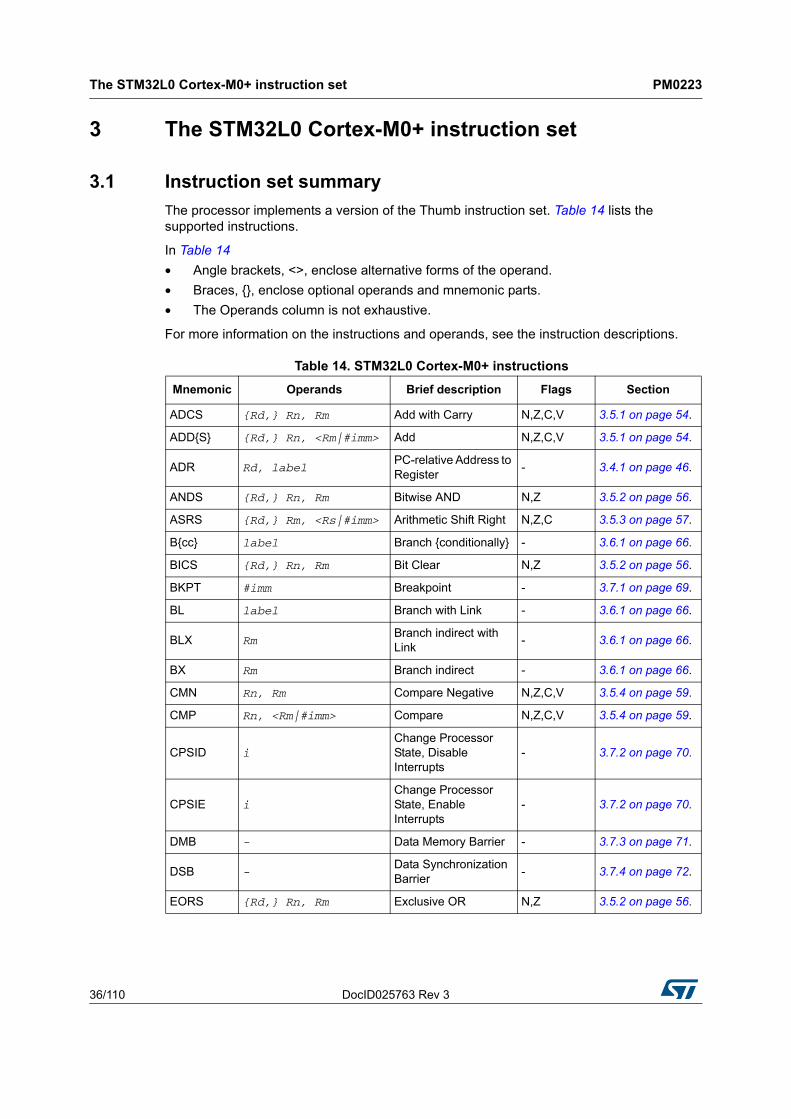
3.1 Instruction set summary
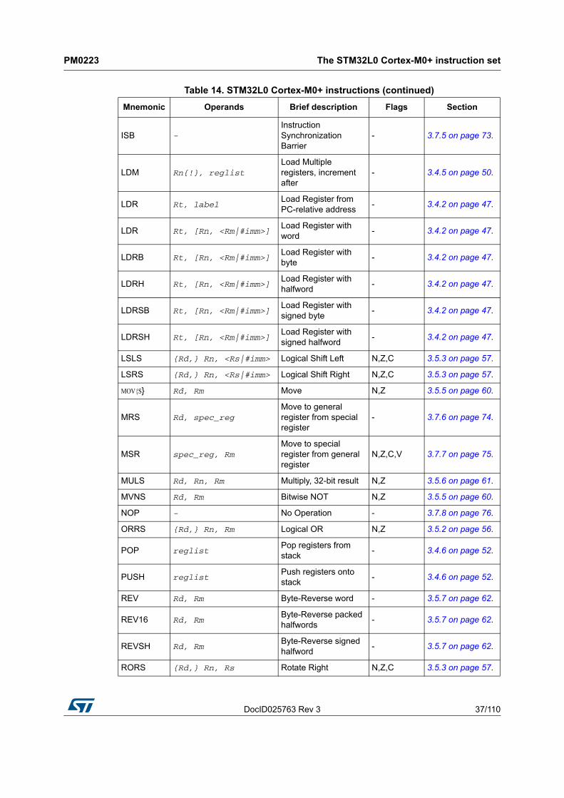
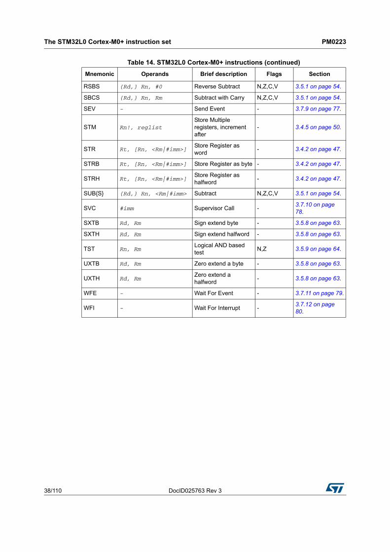
The processor implements a version of the Thumb instruction set. Table 14 lists the supported instructions.
In Table 14
• Angle brackets, <>, enclose alternative forms of the operand.
• Braces, {}, enclose optional operands and mnemonic parts.
• The Operands column is not exhaustive.
For more information on the instructions and operands, see the instruction descriptions.
Table 14. STM32L0 Cortex-M0+ instructions
Mnemonic Operands Brief description Flags Section
ADCS {Rd,} Rn, Rm Add with Carry N,Z,C,V 3.5.1 on page 54.
ADD{S} {Rd,} Rn, <Rm|#imm> Add N,Z,C,V 3.5.1 on page 54.
ADR Rd, labelPC-relative Address to Register
- 3.4.1 on page 46.
ANDS {Rd,} Rn, Rm Bitwise AND N,Z 3.5.2 on page 56.
ASRS {Rd,} Rm, <Rs|#imm> Arithmetic Shift Right N,Z,C 3.5.3 on page 57.
B{cc} label Branch {conditionally} - 3.6.1 on page 66.
BICS {Rd,} Rn, Rm Bit Clear N,Z 3.5.2 on page 56.
BKPT #imm Breakpoint - 3.7.1 on page 69.
BL label Branch with Link - 3.6.1 on page 66.
BLX RmBranch indirect with Link
- 3.6.1 on page 66.
BX Rm Branch indirect - 3.6.1 on page 66.
CMN Rn, Rm Compare Negative N,Z,C,V 3.5.4 on page 59.
CMP Rn, <Rm|#imm> Compare N,Z,C,V 3.5.4 on page 59.
CPSID iChange Processor State, Disable Interrupts
- 3.7.2 on page 70.
CPSIE iChange Processor State, Enable Interrupts
- 3.7.2 on page 70.
DMB - Data Memory Barrier - 3.7.3 on page 71.
DSB -Data Synchronization Barrier
- 3.7.4 on page 72.
EORS {Rd,} Rn, Rm Exclusive OR N,Z 3.5.2 on page 56.
DocID025763 Rev 3 37/110
PM0223 The STM32L0 Cortex-M0+ instruction set
80
ISB -Instruction Synchronization Barrier
- 3.7.5 on page 73.
LDM Rn{!}, reglistLoad Multiple registers, increment after
- 3.4.5 on page 50.
LDR Rt, labelLoad Register from PC-relative address
- 3.4.2 on page 47.
LDR Rt, [Rn, <Rm|#imm>]Load Register with word
- 3.4.2 on page 47.
LDRB Rt, [Rn, <Rm|#imm>]Load Register with byte
- 3.4.2 on page 47.
LDRH Rt, [Rn, <Rm|#imm>]Load Register with halfword
- 3.4.2 on page 47.
LDRSB Rt, [Rn, <Rm|#imm>]Load Register with signed byte
- 3.4.2 on page 47.
LDRSH Rt, [Rn, <Rm|#imm>]Load Register with signed halfword
- 3.4.2 on page 47.
LSLS {Rd,} Rn, <Rs|#imm> Logical Shift Left N,Z,C 3.5.3 on page 57.
LSRS {Rd,} Rn, <Rs|#imm> Logical Shift Right N,Z,C 3.5.3 on page 57.
MOV{S} Rd, Rm Move N,Z 3.5.5 on page 60.
MRS Rd, spec_regMove to general register from special register
- 3.7.6 on page 74.
MSR spec_reg, RmMove to special register from general register
N,Z,C,V 3.7.7 on page 75.
MULS Rd, Rn, Rm Multiply, 32-bit result N,Z 3.5.6 on page 61.
MVNS Rd, Rm Bitwise NOT N,Z 3.5.5 on page 60.
NOP - No Operation - 3.7.8 on page 76.
ORRS {Rd,} Rn, Rm Logical OR N,Z 3.5.2 on page 56.
POP reglistPop registers from stack
- 3.4.6 on page 52.
PUSH reglistPush registers onto stack
- 3.4.6 on page 52.
REV Rd, Rm Byte-Reverse word - 3.5.7 on page 62.
REV16 Rd, RmByte-Reverse packed halfwords
- 3.5.7 on page 62.
REVSH Rd, RmByte-Reverse signed halfword
- 3.5.7 on page 62.
RORS {Rd,} Rn, Rs Rotate Right N,Z,C 3.5.3 on page 57.
Table 14. STM32L0 Cortex-M0+ instructions (continued)
Mnemonic Operands Brief description Flags Section
The STM32L0 Cortex-M0+ instruction set PM0223
38/110 DocID025763 Rev 3
RSBS {Rd,} Rn, #0 Reverse Subtract N,Z,C,V 3.5.1 on page 54.
SBCS {Rd,} Rn, Rm Subtract with Carry N,Z,C,V 3.5.1 on page 54.
SEV - Send Event - 3.7.9 on page 77.
STM Rn!, reglistStore Multiple registers, increment after
- 3.4.5 on page 50.
STR Rt, [Rn, <Rm|#imm>]Store Register as word
- 3.4.2 on page 47.
STRB Rt, [Rn, <Rm|#imm>] Store Register as byte - 3.4.2 on page 47.
STRH Rt, [Rn, <Rm|#imm>]Store Register as halfword
- 3.4.2 on page 47.
SUB{S} {Rd,} Rn, <Rm|#imm> Subtract N,Z,C,V 3.5.1 on page 54.
SVC #imm Supervisor Call -3.7.10 on page 78.
SXTB Rd, Rm Sign extend byte - 3.5.8 on page 63.
SXTH Rd, Rm Sign extend halfword - 3.5.8 on page 63.
TST Rn, RmLogical AND based test
N,Z 3.5.9 on page 64.
UXTB Rd, Rm Zero extend a byte - 3.5.8 on page 63.
UXTH Rd, RmZero extend a halfword
- 3.5.8 on page 63.
WFE - Wait For Event - 3.7.11 on page 79.
WFI - Wait For Interrupt -3.7.12 on page 80.
Table 14. STM32L0 Cortex-M0+ instructions (continued)
Mnemonic Operands Brief description Flags Section
DocID025763 Rev 3 39/110
PM0223 The STM32L0 Cortex-M0+ instruction set
80
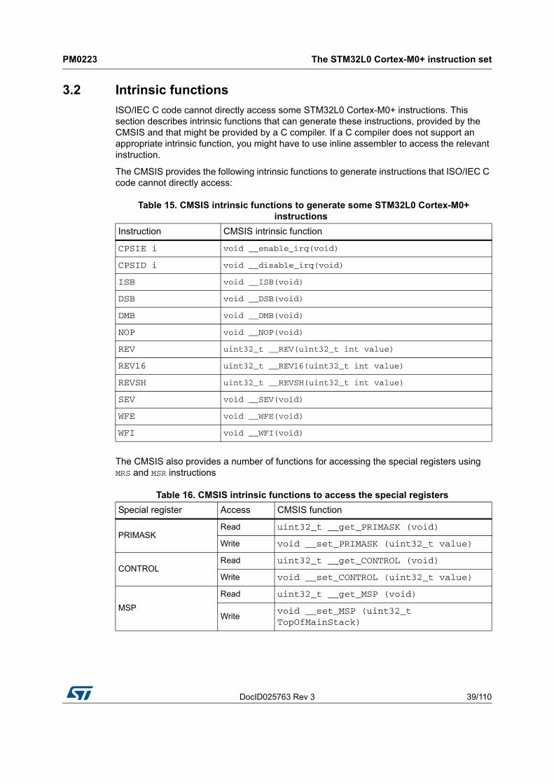
3.2 Intrinsic functions
ISO/IEC C code cannot directly access some STM32L0 Cortex-M0+ instructions. This section describes intrinsic functions that can generate these instructions, provided by the CMSIS and that might be provided by a C compiler. If a C compiler does not support an appropriate intrinsic function, you might have to use inline assembler to access the relevant instruction.
The CMSIS provides the following intrinsic functions to generate instructions that ISO/IEC C code cannot directly access:
The CMSIS also provides a number of functions for accessing the special registers using MRS and MSR instructions
:
Table 15. CMSIS intrinsic functions to generate some STM32L0 Cortex-M0+ instructions
Instruction CMSIS intrinsic function
CPSIE i void __enable_irq(void)
CPSID i void __disable_irq(void)
ISB void __ISB(void)
DSB void __DSB(void)
DMB void __DMB(void)
NOP void __NOP(void)
REV uint32_t __REV(uint32_t int value)
REV16 uint32_t __REV16(uint32_t int value)
REVSH uint32_t __REVSH(uint32_t int value)
SEV void __SEV(void)
WFE void __WFE(void)
WFI void __WFI(void)
Table 16. CMSIS intrinsic functions to access the special registers
Special register Access CMSIS function
PRIMASKRead uint32_t __get_PRIMASK (void)
Write void __set_PRIMASK (uint32_t value)
CONTROLRead uint32_t __get_CONTROL (void)
Write void __set_CONTROL (uint32_t value)
MSP
Read uint32_t __get_MSP (void)
Writevoid __set_MSP (uint32_t TopOfMainStack)
The STM32L0 Cortex-M0+ instruction set PM0223
40/110 DocID025763 Rev 3
3.3 About the instruction descriptions
The following sections give more information about using the instructions:
• Operands.
• Restrictions when using PC or SP.
• Shift operations.
• Address alignment.
• PC-relative expressions.
• Conditional execution.
3.3.1 Operands
An instruction operand can be an Arm® register, a constant, or another instruction-specific parameter. Instructions act on the operands and often store the result in a destination register. When there is a destination register in the instruction, it is usually specified before the other operands.
3.3.2 Restrictions when using PC or SP
Many instructions are unable to use, or have restrictions on whether you can use, the Program Counter (PC) or Stack Pointer (SP) for the operands or destination register. See instruction descriptions for more information.
Note: When you update the PC with a BX, BLX, or POP instruction, bit[0] of any address must be 1 for correct execution. This is because this bit indicates the destination instruction set, and the STM32L0 Cortex-M0+ processor only supports Thumb instructions. When a BL or BLX instruction writes the value of bit[0] into the LR it is automatically assigned the value 1.
3.3.3 Shift operations
Register shift operations move the bits in a register left or right by a specified number of bits, the shift length. Register shift can be performed directly by the instructions ASR, LSR, LSL, and ROR and the result is written to a destination register.
The permitted shift lengths depend on the shift type and the instruction, see the individual instruction description. If the shift length is 0, no shift occurs. Register shift operations update the carry flag except when the specified shift length is 0. The following sub-sections describe the various shift operations and how they affect the carry flag. In these descriptions, Rm is the register containing the value to be shifted, and n is the shift length.
ASR
Arithmetic shift right by n bits moves the left-hand 32-n bits of the register Rm, to the right by n places, into the right-hand 32-n bits of the result, and it copies the original bit[31] of the
PSP
Read uint32_t __get_PSP (void)
Writevoid __set_PSP (uint32_t TopOfProcStack)
Table 16. CMSIS intrinsic functions to access the special registers (continued)
Special register Access CMSIS function
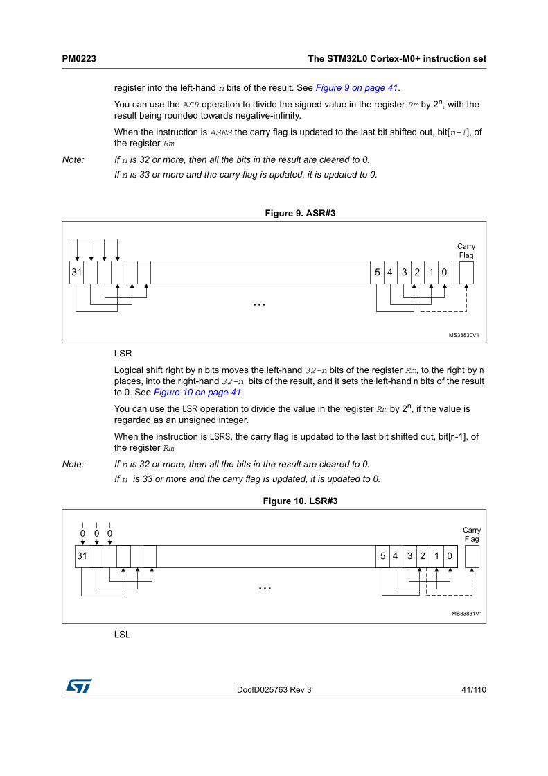
DocID025763 Rev 3 41/110
PM0223 The STM32L0 Cortex-M0+ instruction set
80
register into the left-hand n bits of the result. See Figure 9 on page 41.
You can use the ASR operation to divide the signed value in the register Rm by 2n, with the result being rounded towards negative-infinity.
When the instruction is ASRS the carry flag is updated to the last bit shifted out, bit[n-1], of the register Rm
Note: If n is 32 or more, then all the bits in the result are cleared to 0.
If n is 33 or more and the carry flag is updated, it is updated to 0.
Figure 9. ASR#3
LSR
Logical shift right by n bits moves the left-hand 32-n bits of the register Rm, to the right by n places, into the right-hand 32-n bits of the result, and it sets the left-hand n bits of the result to 0. See Figure 10 on page 41.
You can use the LSR operation to divide the value in the register Rm by 2n, if the value is regarded as an unsigned integer.
When the instruction is LSRS, the carry flag is updated to the last bit shifted out, bit[n-1], of the register Rm.
Note: If n is 32 or more, then all the bits in the result are cleared to 0.
If n is 33 or more and the carry flag is updated, it is updated to 0.
Figure 10. LSR#3
LSL
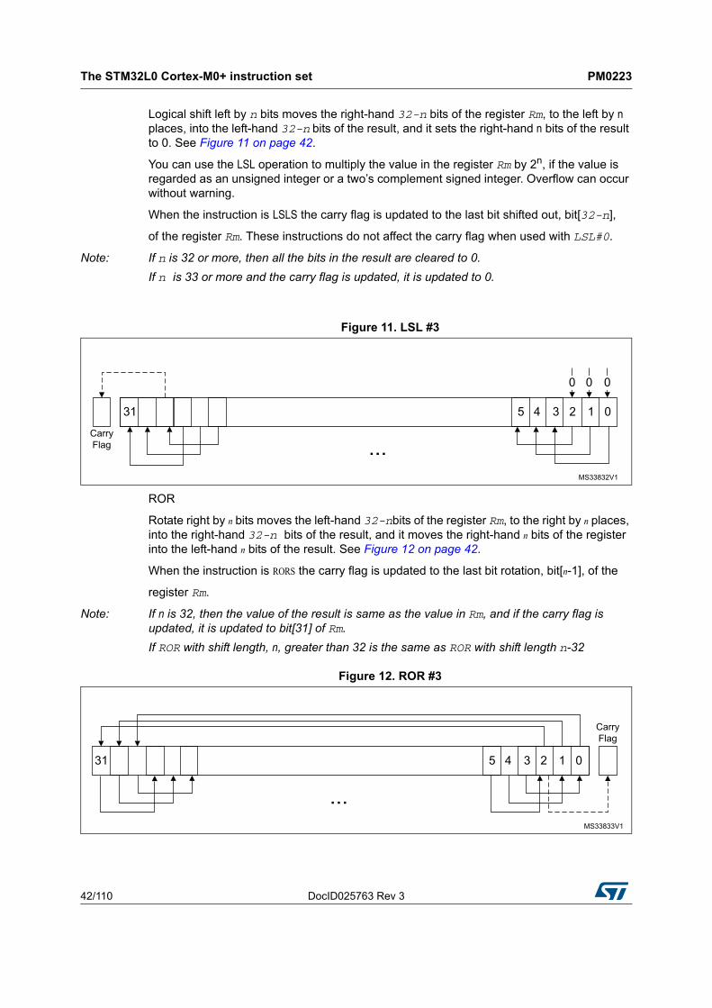
The STM32L0 Cortex-M0+ instruction set PM0223
42/110 DocID025763 Rev 3
Logical shift left by n bits moves the right-hand 32-n bits of the register Rm, to the left by n places, into the left-hand 32-n bits of the result, and it sets the right-hand n bits of the result to 0. See Figure 11 on page 42.
You can use the LSL operation to multiply the value in the register Rm by 2n, if the value is regarded as an unsigned integer or a two’s complement signed integer. Overflow can occur without warning.
When the instruction is LSLS the carry flag is updated to the last bit shifted out, bit[32-n],
of the register Rm. These instructions do not affect the carry flag when used with LSL#0.
Note: If n is 32 or more, then all the bits in the result are cleared to 0.
If n is 33 or more and the carry flag is updated, it is updated to 0.
Figure 11. LSL #3
ROR
Rotate right by n bits moves the left-hand 32-nbits of the register Rm, to the right by n places, into the right-hand 32-n bits of the result, and it moves the right-hand n bits of the register into the left-hand n bits of the result. See Figure 12 on page 42.
When the instruction is RORS the carry flag is updated to the last bit rotation, bit[n-1], of the
register Rm.
Note: If n is 32, then the value of the result is same as the value in Rm, and if the carry flag is updated, it is updated to bit[31] of Rm.
If ROR with shift length, n, greater than 32 is the same as ROR with shift length n-32
Figure 12. ROR #3
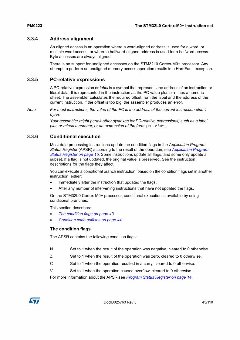
DocID025763 Rev 3 43/110
PM0223 The STM32L0 Cortex-M0+ instruction set
80
3.3.4 Address alignment
An aligned access is an operation where a word-aligned address is used for a word, or multiple word access, or where a halfword-aligned address is used for a halfword access. Byte accesses are always aligned.
There is no support for unaligned accesses on the STM32L0 Cortex-M0+ processor. Any attempt to perform an unaligned memory access operation results in a HardFault exception.
3.3.5 PC-relative expressions
A PC-relative expression or label is a symbol that represents the address of an instruction or literal data. It is represented in the instruction as the PC value plus or minus a numeric offset. The assembler calculates the required offset from the label and the address of the current instruction. If the offset is too big, the assembler produces an error.
Note: For most instructions, the value of the PC is the address of the current instruction plus 4 bytes.
Your assembler might permit other syntaxes for PC-relative expressions, such as a label plus or minus a number, or an expression of the form [PC,#imm].
3.3.6 Conditional execution
Most data processing instructions update the condition flags in the Application Program Status Register (APSR) according to the result of the operation, see Application Program Status Register on page 15. Some instructions update all flags, and some only update a subset. If a flag is not updated, the original value is preserved. See the instruction descriptions for the flags they affect.
You can execute a conditional branch instruction, based on the condition flags set in another instruction, either:
• Immediately after the instruction that updated the flags.
• After any number of intervening instructions that have not updated the flags.
On the STM32L0 Cortex-M0+ processor, conditional execution is available by using conditional branches.
This section describes:
• The condition flags on page 43.
• Condition code suffixes on page 44.
The condition flags
The APSR contains the following condition flags:
For more information about the APSR see Program Status Register on page 14.
N Set to 1 when the result of the operation was negative, cleared to 0 otherwise
Z Set to 1 when the result of the operation was zero, cleared to 0 otherwise.
C Set to 1 when the operation resulted in a carry, cleared to 0 otherwise.
V Set to 1 when the operation caused overflow, cleared to 0 otherwise.
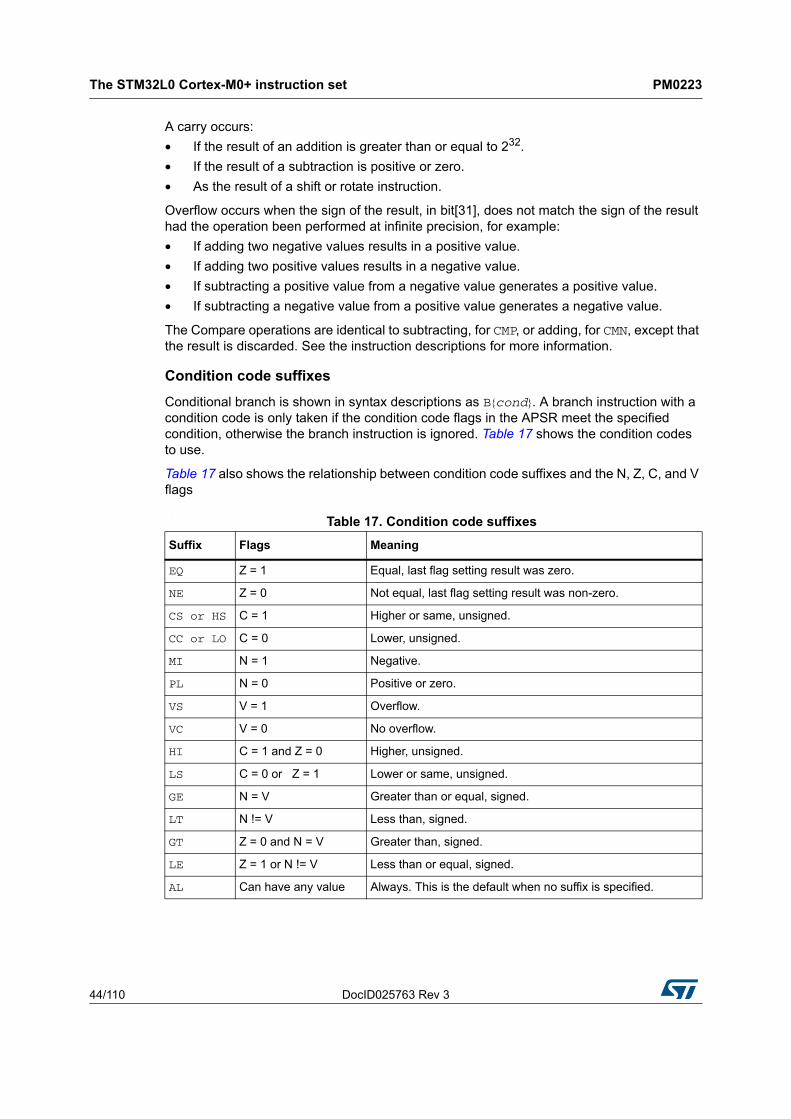
The STM32L0 Cortex-M0+ instruction set PM0223
44/110 DocID025763 Rev 3
A carry occurs:
• If the result of an addition is greater than or equal to 232.
• If the result of a subtraction is positive or zero.
• As the result of a shift or rotate instruction.
Overflow occurs when the sign of the result, in bit[31], does not match the sign of the result had the operation been performed at infinite precision, for example:
• If adding two negative values results in a positive value.
• If adding two positive values results in a negative value.
• If subtracting a positive value from a negative value generates a positive value.
• If subtracting a negative value from a positive value generates a negative value.
The Compare operations are identical to subtracting, for CMP, or adding, for CMN, except that the result is discarded. See the instruction descriptions for more information.
Condition code suffixes
Conditional branch is shown in syntax descriptions as B{cond}. A branch instruction with a condition code is only taken if the condition code flags in the APSR meet the specified condition, otherwise the branch instruction is ignored. Table 17 shows the condition codes to use.
Table 17 also shows the relationship between condition code suffixes and the N, Z, C, and V flags
.
Table 17. Condition code suffixes
Suffix Flags Meaning
EQ Z = 1 Equal, last flag setting result was zero.
NE Z = 0 Not equal, last flag setting result was non-zero.
CS or HS C = 1 Higher or same, unsigned.
CC or LO C = 0 Lower, unsigned.
MI N = 1 Negative.
PL N = 0 Positive or zero.
VS V = 1 Overflow.
VC V = 0 No overflow.
HI C = 1 and Z = 0 Higher, unsigned.
LS C = 0 or Z = 1 Lower or same, unsigned.
GE N = V Greater than or equal, signed.
LT N != V Less than, signed.
GT Z = 0 and N = V Greater than, signed.
LE Z = 1 or N != V Less than or equal, signed.
AL Can have any value Always. This is the default when no suffix is specified.
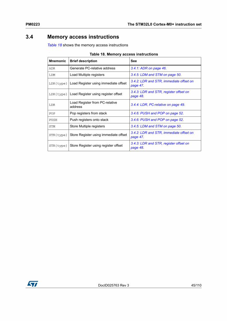
DocID025763 Rev 3 45/110
PM0223 The STM32L0 Cortex-M0+ instruction set
80
3.4 Memory access instructions
Table 18 shows the memory access instructions
:
Table 18. Memory access instructions
Mnemonic Brief description See
ADR Generate PC-relative address 3.4.1: ADR on page 46.
LDM Load Multiple registers 3.4.5: LDM and STM on page 50.
LDR{type} Load Register using immediate offset3.4.2: LDR and STR, immediate offset on page 47.
LDR{type} Load Register using register offset3.4.3: LDR and STR, register offset on page 48.
LDRLoad Register from PC-relative address
3.4.4: LDR, PC-relative on page 49.
POP Pop registers from stack 3.4.6: PUSH and POP on page 52.
PUSH Push registers onto stack 3.4.6: PUSH and POP on page 52.
STM Store Multiple registers 3.4.5: LDM and STM on page 50.
STR{type} Store Register using immediate offset3.4.2: LDR and STR, immediate offset on page 47.
STR{type} Store Register using register offset3.4.3: LDR and STR, register offset on page 48.
The STM32L0 Cortex-M0+ instruction set PM0223
46/110 DocID025763 Rev 3
3.4.1 ADR
Generates a PC-relative address.
Syntax
ADR Rd, label
where:
Operation
ADR generates an address by adding an immediate value to the PC, and writes the result to the destination register.
ADR facilitates the generation of position-independent code, because the address is PC-relative.
If you use ADR to generate a target address for a BX or BLX instruction, you must ensure that bit[0] of the address you generate is set to 1 for correct execution.
Restrictions
In this instruction Rd must specify R0-R7. The data-value addressed must be word aligned and within 1020 bytes of the current PC.
Condition flags
This instruction does not change the flags.
Examples
ADR R1, TextMessage ; Write address value of a location labelled as;
TextMessage to R1
ADR R3, [PC,#996] ; Set R3 to value of PC + 996.
Rd Is the destination register.
label Is a PC-relative expression. See 3.3.5: PC-relative expressions on page 43.
DocID025763 Rev 3 47/110
PM0223 The STM32L0 Cortex-M0+ instruction set
80
3.4.2 LDR and STR, immediate offset
Load and Store with immediate offset.
Syntax
LDR Rt, [<Rn | SP> {, #imm}]
LDR<B|H> Rt, [Rn {, #imm}]
STR Rt, [<Rn | SP>, {,#imm}]
STR<B|H> Rt, [Rn {,#imm}]
where:
Operation
LDR, LDRB and LDRH instructions load the register specified by Rt with either a word, byte or halfword data value from memory. Sizes less than word are zero extended to 32-bits before being written to the register specified by Rt.
STR, STRB and STRH instructions store the word, least-significant byte or lower halfword contained in the single register specified by Rt in to memory. The memory address to load from or store to is the sum of the value in the register specified by either Rn or SP and the immediate value imm.
Restrictions
In these instructions:
• Rt and Rn must only specify R0-R7.
• imm must be between:
– 0 and 1020 and an integer multiple of four for LDR and STR using SP as the base register.
– 0 and 124 and an integer multiple of four for LDR and STR using R0-R7 as the base register.
– 0 and 62 and an integer multiple of two for LDRH and STRH.
– 0 and 31 for LDRB and STRB.
• The computed address must be divisible by the number of bytes in the transaction, see 3.3.4: Address alignment on page 43.
Condition flags
These instructions do not change the flags.
Examples
LDR R4, [R7 ; Loads R4 from the address in R7.
STR R2,[R0,#const-struc] ; const-struc is an expression evaluating
; to a constant in the range 0-1020.
Rt Is the register to load or store.
Rn Is the register on which the memory address is based
imm Is an offset from Rn. If imm is omitted, it is assumed to be zero.
The STM32L0 Cortex-M0+ instruction set PM0223
48/110 DocID025763 Rev 3
3.4.3 LDR and STR, register offset
Load and Store with register offset.
Syntax
LDR Rt, [Rn, Rm]
LDR<B|H> Rt, [Rn, Rm]
LDR<SB|SH> Rt, [Rn, Rm]
STR Rt, [Rn, Rm]
STR<B|H> Rt, [Rn, Rm]
where:
Operation
LDR, LDRB, LDRH, LDRSB and LDRSH load the register specified by Rt with either a word, zero extended byte, zero extended halfword, sign extended byte or sign extended halfword value from memory.
STR, STRB and STRH store the word, least-significant byte or lower halfword contained in the single register specified by Rt into memory.
The memory address to load from or store to is the sum of the values in the registers specified by Rn and Rm.
Restrictions
In these instructions:
• Rt, Rn, and Rm must only specify R0-R7.
• The computed memory address must be divisible by the number of bytes in the load or store, see 3.3.4: Address alignment on page 43.
Condition flags
These instructions do not change the flags.
Examples
STR R0, [R5, R1] ; Store value of R0 into an address equal to ; sum of R5 and R1 LDRSH R1, [R2, R3] ; Load a halfword from the memory address ; specified by (R2 + R3), sign extend to 32-bits ; and write to R1.
Rt Is the register to load or store.
Rn Is the register on which the memory address is based
Rm s a register containing a value to be used as the offset
DocID025763 Rev 3 49/110
PM0223 The STM32L0 Cortex-M0+ instruction set
80
3.4.4 LDR, PC-relative
Load register (literal) from memory.
Syntax
LDR Rt, label
where:
Operation
Loads the register specified by Rt from the word in memory specified by label.
Restrictions
In these instructions, label must be within 1020 bytes of the current PC and word aligned.
Condition flags
These instructions do not change the flags.
Examples
LDR R0, LookUpTable ; Load R0 with a word of data from an address ; labelled as LookUpTable. LDR R3, [PC, #100] ; Load R3 with memory word at (PC + 100).
Rt Is the register to load
label Is a PC-relative expression. See 3.3.5: PC-relative expressions on page 43.
The STM32L0 Cortex-M0+ instruction set PM0223
50/110 DocID025763 Rev 3
3.4.5 LDM and STM
Load and Store Multiple registers.
Syntax
LDM Rn{!}, reglist
STM Rn!, reglist
where:
LDMIA and LDMFD are synonyms for LDM. LDMIA refers to the base register being Incremented After each access. LDMFD refers to its use for popping data from Full Descending stacks.
STMIA and STMEA are synonyms for STM. STMIA refers to the base register being Incremented After each access. STMEA refers to its use for pushing data onto Empty Ascending stacks.
Operation
LDM instructions load the registers in reglist with word values from memory addresses based on Rn.
STM instructions store the word values in the registers in reglist to memory addresses based on Rn.
The memory addresses used for the accesses are at 4-byte intervals ranging from the value in the register specified by Rn to the value in the register specified by Rn + 4 * (n-1), where n is the number of registers in reglist. The accesses happens in order of increasing register numbers, with the lowest numbered register using the lowest memory address and the highest number register using the highest memory address. If the writeback suffix is specified, the value in the register specified by Rn + 4 *n is written back to the register specified by Rn.
Restrictions
In these instructions:
• reglist and Rn are limited to R0-R7.
• The writeback suffix must always be used unless the instruction is an LDM where reglist also contains Rn, in which case the writeback suffix must not be used.
• The value in the register specified by Rn must be word aligned. See 3.3.4: Address alignment on page 43 for more information.
• For STM, if Rn appears in reglist, then it must be the first register in the list.
Condition flags
These instructions do not change the flags.
Rn Is the register on which the memory addresses are based.
! Writeback suffix.
reglist Is a list of one or more registers to be loaded or stored, enclosed in braces. It can contain register ranges. It must be comma separated if it contains more than one register or register range, see Examples on page 51.
DocID025763 Rev 3 51/110
PM0223 The STM32L0 Cortex-M0+ instruction set
80
Examples
LDM R0,{R0,R3,R4} ; LDMIA is a synonym for LDM STMIA R1!,{R2-R4,R6}
Incorrect examples
STM R5!,{R4,R5,R6} ;Value stored for R5 is unpredictable LDM R2,{} ;There must be at least one register in the list
The STM32L0 Cortex-M0+ instruction set PM0223
52/110 DocID025763 Rev 3
3.4.6 PUSH and POP
Push registers onto, and pop registers off a full-descending stack.
Syntax
PUSH reglist
POP reglist
where:
Operation
PUSH stores registers on the stack, with the lowest numbered register using the lowest memory address and the highest numbered register using the highest memory address.
POP loads registers from the stack, with the lowest numbered register using the lowest memory address and the highest numbered register using the highest memory address.
PUSH uses the value in the SP register minus four as the highest memory address, POP uses the value in the SP register as the lowest memory address, implementing a full-descending stack. On completion, PUSH updates the SP register to point to the location of the lowest store value, POP updates the SP register to point to the location above the highest location loaded.
If a POP instruction includes PC in its reglist, a branch to this location is performed when the POP instruction has completed. Bit[0] of the value read for the PC is used to update the APSR T-bit. This bit must be 1 to ensure correct operation.
Restrictions
In these instructions:
• reglist must use only R0-R7.
• The exception is LR for a PUSH and PC for a POP.
Condition flags
These instructions do not change the flags.
Examples
PUSH {R0,R4-R7} ; Push R0,R4,R5,R6,R7 onto the stack PUSH {R2,LR} ; Push R2 and the link-register onto the stack POP {R0,R6,PC} ; Pop r0,r6 and PC from the stack, then branch to ; the new PC.
reglist Is a non-empty list of registers, enclosed in braces. It can contain register ranges. It must be comma separated if it contains more than one register or register range.
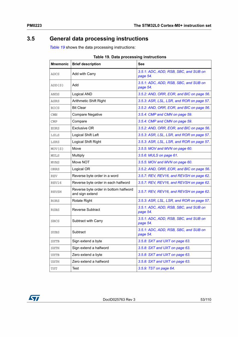
DocID025763 Rev 3 53/110
PM0223 The STM32L0 Cortex-M0+ instruction set
80
3.5 General data processing instructions
Table 19 shows the data processing instructions:
Table 19. Data processing instructions
Mnemonic Brief description See
ADCS Add with Carry3.5.1: ADC, ADD, RSB, SBC, and SUB on page 54.
ADD{S} Add3.5.1: ADC, ADD, RSB, SBC, and SUB on page 54.
ANDS Logical AND 3.5.2: AND, ORR, EOR, and BIC on page 56.
ASRS Arithmetic Shift Right 3.5.3: ASR, LSL, LSR, and ROR on page 57.
BICS Bit Clear 3.5.2: AND, ORR, EOR, and BIC on page 56.
CMN Compare Negative 3.5.4: CMP and CMN on page 59.
CMP Compare 3.5.4: CMP and CMN on page 59.
EORS Exclusive OR 3.5.2: AND, ORR, EOR, and BIC on page 56.
LSLS Logical Shift Left 3.5.3: ASR, LSL, LSR, and ROR on page 57.
LSRS Logical Shift Right 3.5.3: ASR, LSL, LSR, and ROR on page 57.
MOV{S} Move 3.5.5: MOV and MVN on page 60.
MULS Multiply 3.5.6: MULS on page 61.
MVNS Move NOT 3.5.5: MOV and MVN on page 60.
ORRS Logical OR 3.5.2: AND, ORR, EOR, and BIC on page 56.
REV Reverse byte order in a word 3.5.7: REV, REV16, and REVSH on page 62.
REV16 Reverse byte order in each halfword 3.5.7: REV, REV16, and REVSH on page 62.
REVSHReverse byte order in bottom halfword and sign extend
3.5.7: REV, REV16, and REVSH on page 62.
RORS Rotate Right 3.5.3: ASR, LSL, LSR, and ROR on page 57.
RSBS Reverse Subtract3.5.1: ADC, ADD, RSB, SBC, and SUB on page 54.
SBCS Subtract with Carry3.5.1: ADC, ADD, RSB, SBC, and SUB on page 54.
SUBS Subtract3.5.1: ADC, ADD, RSB, SBC, and SUB on page 54.
SXTB Sign extend a byte 3.5.8: SXT and UXT on page 63.
SXTH Sign extend a halfword 3.5.8: SXT and UXT on page 63.
UXTB Zero extend a byte 3.5.8: SXT and UXT on page 63.
UXTH Zero extend a halfword 3.5.8: SXT and UXT on page 63.
TST Test 3.5.9: TST on page 64.
The STM32L0 Cortex-M0+ instruction set PM0223
54/110 DocID025763 Rev 3
3.5.1 ADC, ADD, RSB, SBC, and SUB
Add with carry, Add, Reverse Subtract, Subtract with carry, and Subtract.
Syntax
ADCS {Rd,} Rn, Rm
ADD{S} {Rd,} Rn, <Rm|#imm>
RSBS {Rd,} Rn, Rm, #0
SBCS {Rd,} Rn, Rm
SUB{S} {Rd,} Rn, <Rm|#imm>
Where:
When the optional Rd register specifier is omitted, it is assumed to take the same value as Rn, for example ADDS R1,R2 is identical to ADDS R1,R1,R2.
Operation
The ADCS instruction adds the value in Rn to the value in Rm, adding another one if the carry flag is set, places the result in the register specified by Rd and updates the N, Z, C, and V flags.
The ADD instruction adds the value in Rn to the value in Rm or an immediate value specified by imm and places the result in the register specified by Rd.
The ADDS instruction performs the same operation as ADD and also updates the N, Z, C and V flags.
The RSBS instruction subtracts the value in Rn from zero, producing the arithmetic negative of the value, and places the result in the register specified by Rd and updates the N, Z, C and V flags.
The SBCS instruction subtracts the value of Rm from the value in Rn, if the carry flag is clear, the result is reduced by one. It places the result in the register specified by Rd and updates the N, Z, C and V flags.
The SUB instruction subtracts the value in Rm or the immediate specified by imm. It places the result in the register specified by Rd.
The SUBS instruction performs the same operation as SUB and also updates the N, Z, C and V flags.
Use ADC and SBC to synthesize multiword arithmetic, see Examples on page 55.
See also 3.4.1: ADR on page 46.
Restrictions
Table 20 lists the legal combinations of register specifiers and immediate values that can be used with each instruction.
S Causes an ADD or SUB instruction to update flags.
Rd Specifies the result register.
reglist Specifies the first source register.
Imm Specifies a constant immediate value.
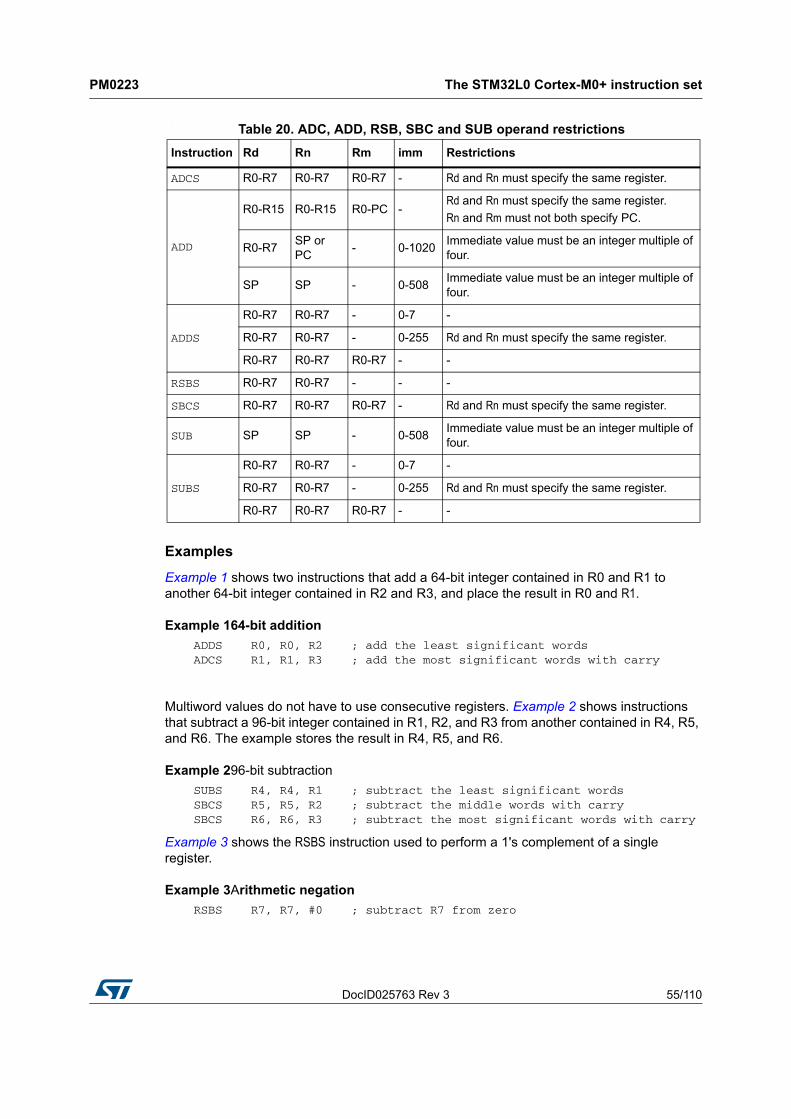
DocID025763 Rev 3 55/110
PM0223 The STM32L0 Cortex-M0+ instruction set
80
.
Examples
Example 1 shows two instructions that add a 64-bit integer contained in R0 and R1 to another 64-bit integer contained in R2 and R3, and place the result in R0 and R1.
Example 164-bit addition
ADDS R0, R0, R2 ; add the least significant words ADCS R1, R1, R3 ; add the most significant words with carry
Multiword values do not have to use consecutive registers. Example 2 shows instructions that subtract a 96-bit integer contained in R1, R2, and R3 from another contained in R4, R5, and R6. The example stores the result in R4, R5, and R6.
Example 296-bit subtraction
SUBS R4, R4, R1 ; subtract the least significant words SBCS R5, R5, R2 ; subtract the middle words with carry SBCS R6, R6, R3 ; subtract the most significant words with carry
Example 3 shows the RSBS instruction used to perform a 1's complement of a single register.
Example 3Arithmetic negation
RSBS R7, R7, #0 ; subtract R7 from zero
Table 20. ADC, ADD, RSB, SBC and SUB operand restrictions
Instruction Rd Rn Rm imm Restrictions
ADCS R0-R7 R0-R7 R0-R7 - Rd and Rn must specify the same register.
ADD
R0-R15 R0-R15 R0-PC -Rd and Rn must specify the same register.
Rn and Rm must not both specify PC.
R0-R7SP or PC
- 0-1020Immediate value must be an integer multiple of four.
SP SP - 0-508Immediate value must be an integer multiple of four.
ADDS
R0-R7 R0-R7 - 0-7 -
R0-R7 R0-R7 - 0-255 Rd and Rn must specify the same register.
R0-R7 R0-R7 R0-R7 - -
RSBS R0-R7 R0-R7 - - -
SBCS R0-R7 R0-R7 R0-R7 - Rd and Rn must specify the same register.
SUB SP SP - 0-508Immediate value must be an integer multiple of four.
SUBS
R0-R7 R0-R7 - 0-7 -
R0-R7 R0-R7 - 0-255 Rd and Rn must specify the same register.
R0-R7 R0-R7 R0-R7 - -
The STM32L0 Cortex-M0+ instruction set PM0223
56/110 DocID025763 Rev 3
3.5.2 AND, ORR, EOR, and BIC
Logical AND, OR, Exclusive OR, and Bit Clear.
Syntax
ANDS {Rd,} Rn, Rm
ORRS {Rd,} Rn, Rm
EORS {Rd,} Rn, Rm
BICS {Rd,} Rn, Rm
where:
Operation
The AND, EOR, and ORR instructions perform bitwise AND, exclusive OR, and inclusive OR operations on the values in Rn and Rm.
The BIC instruction performs an AND operation on the bits in Rn with the logical negation of the corresponding bits in the value of Rm.
The condition code flags are updated on the result of the operation, see Condition flags on page 47.
Restrictions
In these instructions, Rd, Rn, and Rm must only specify R0-R7.
Condition flags
These instructions:
Update the N and Z flags according to the result.
Do not affect the C or V flag.
Examples
ANDS R2, R2, R1 ORRS R2, R2, R5 ANDS R5, R5, R8 EORS R7, R7, R6 BICS R0, R0, R1
Rd Is the destination register.
Rn Is the register holding the first operand and is the same as the destination register.
Rm Second register
DocID025763 Rev 3 57/110
PM0223 The STM32L0 Cortex-M0+ instruction set
80
3.5.3 ASR, LSL, LSR, and ROR
Arithmetic Shift Right, Logical Shift Left, Logical Shift Right, and Rotate Right.
Syntax
ASRS {Rd,} Rm, Rs
ASRS {Rd,} Rm, #imm
LSLS {Rd,} Rm, Rs
LSLS {Rd,} Rm, #imm
LSRS {Rd,} Rm, Rs
LSRS {Rd,} Rm, #imm
RORS {Rd,} Rm, Rs
where:
Note: MOVS Rd, Rm is a pseudonym for LSLS Rd, Rm, #0.
Operation
ASR, LSL, LSR, and ROR perform an arithmetic-shift-left, logical-shift-left, logical-shift-right or a right-rotation of the bits in the register Rm by the number of places specified by the immediate imm or the value in the least-significant byte of the register specified by Rs.
For details on what result is generated by the different instructions, see 3.3.3: Shift operations on page 40.
Restrictions
In these instructions, Rd, Rm, and Rs must only specify R0-R7. For non-immediate instructions, Rd and Rm must specify the same register.
Condition flags
These instructions update the N and Z flags according to the result.
The C flag is updated to the last bit shifted out, except when the shift length is 0, see 3.3.3: Shift operations on page 40. The V flag is left unmodified.
Rd Is the destination register. If Rd is omitted, it is assumed to take the same value as Rm.
Rm Is the register holding the value to be shifted.
Rs Is the register holding the shift length to apply to the value in Rm
Imm Is the shift length. The range of shift length depends on the instruction:
ASR shift length from 1 to 32
LSL shift length from 0 to 31
LSR shift length from 1 to 32.
The STM32L0 Cortex-M0+ instruction set PM0223
58/110 DocID025763 Rev 3
Examples
ASRS R7, R5, #9 ; Arithmetic shift right by 9 bits LSLS R1, R2, #3 ; Logical shift left by 3 bits with flag update LSRS R4, R5, #6 ; Logical shift right by 6 bits RORS R4, R4, R6 ; Rotate right by the value in the bottom byte of R6.
DocID025763 Rev 3 59/110
PM0223 The STM32L0 Cortex-M0+ instruction set
80
3.5.4 CMP and CMN
Compare and Compare Negative.
Syntax
CMN Rn, Rm
CMP Rn, #imm
CMP Rn, Rm
where:
Operation
These instructions compare the value in a register with either the value in another register or an immediate value. They update the condition flags on the result, but do not write the result to a register.
The CMP instruction subtracts either the value in the register specified by Rm, or the immediate imm from the value in Rn and updates the flags. This is the same as a SUBS instruction, except that the result is discarded.
The CMN instruction adds the value of Rm to the value in Rn and updates the flags. This is the same as an ADDS instruction, except that the result is discarded.
Restrictions
For the:
• CMN instruction Rn, and Rm must only specify R0-R7.
• CMP instruction:
– Rn and Rm can specify R0-R14.
– Immediate must be in the range 0-255.
Condition flags
These instructions update the N, Z, C and V flags according to the result.
Examples
CMP R2, R9 CMN R0, R2
Rn Is the register holding the first operand.
Rm Is the register to compare with.
Imm Is the immediate value to compare with.
The STM32L0 Cortex-M0+ instruction set PM0223
60/110 DocID025763 Rev 3
3.5.5 MOV and MVN
Move and Move NOT.
Syntax
MOV{S} Rd, Rm
MOVS Rd, #imm
MVNS Rd, Rm
where:
Operation
The MOV instruction copies the value of Rm into Rd.
The MOVS instruction performs the same operation as the MOV instruction, but also updates the N and Z flags.
The MVSN instruction takes the value of Rm, performs a bitwise logical negate operation on the value, and places the result into Rd.
Restrictions
In these instructions, Rd, and Rm must only specify R0-R7.
When Rd is the PC in a MOV instruction:
• Bit[0] of the result is discarded.
• A branch occurs to the address created by forcing bit[0] of the result to 0. The T-bit remains unmodified.
Note: Though it is possible to use MOV as a branch instruction, Arm® strongly recommends the use of a BX or BLX instruction to branch for software portability.
Condition flags
If S is specified, these instructions:
• update the N and Z flags according to the result
• do not affect the C or V flags.
Example
MOVS R0, #0x000B ; Write value of 0x000B to R0, flags get updated MOVS R1, #0x0 ; Write value of zero to R1, flags are updated MOV R10, R12 ; Write value in R12 to R10, flags are not updated MOVS R3, #23 ; Write value of 23 to R3 MOV R8, SP ; Write value of stack pointer to R8 MVNS R2, R0 ; Write inverse of R0 to the R2 and update flags
S Is an optional suffix. If S is specified, the condition code flags are updated on the result of the operation, see 3.3.6: Conditional execution on page 43.
Rd Is the destination register.
Rm Is a register.
Imm Is any value in the range 0-255.
DocID025763 Rev 3 61/110
PM0223 The STM32L0 Cortex-M0+ instruction set
80
3.5.6 MULS
Multiply using 32-bit operands, and producing a 32-bit result.
Syntax
MULS Rd, Rn, Rm
where:
Operation
The MUL instruction multiplies the values in the registers specified by Rn and Rm, and places the least significant 32 bits of the result in Rd. The condition code flags are updated on the result of the operation, see 3.3.6: Conditional execution on page 43.
The results of this instruction does not depend on whether the operands are signed or unsigned.
Restrictions
In this instruction:
• Rd, Rn, and Rm must only specify R0-R7.
• Rd must be the same as Rm.
Condition flags
This instruction:
• Updates the N and Z flags according to the result.
• Does not affect the C or V flags.
Examples
MULS R0, R2, R0 ; Multiply with flag update, R0 = R0 x R2
Rd Is the destination register.
Rn, Rm Ire registers holding the values to be multiplied.
The STM32L0 Cortex-M0+ instruction set PM0223
62/110 DocID025763 Rev 3
3.5.7 REV, REV16, and REVSH
Reverse bytes.
Syntax
REV Rd, Rn
REV16 Rd, Rn
REVSH Rd, Rn
where:
Operation
Use these instructions to change endianness of data:
RER
Restrictions
In these instructions, Rd, and Rn must only specify R0-R7.
Condition flags
These instructions do not change the flags.
Examples
REV R3, R7 ; Reverse byte order of value in R7 and write it to R3 REV16 R0, R0 ; Reverse byte order of each 16-bit halfword in R0 REVSH R0, R5 ; Reverse signed halfword
Rd Is the destination register.
Rn Is the source register.
REV Converts 32-bit big-endian data into little-endian data or 32-bit little-endian data into big-endian data.
REV16 Converts two packed 16-bit big-endian data into little-endian data or two packed 16-bit little-endian data into big-endian data.
REVSH Converts 16-bit signed big-endian data into 32-bit signed little-endian data or 16-bit signed little-endian data into 32-bit signed big-endian data.
DocID025763 Rev 3 63/110
PM0223 The STM32L0 Cortex-M0+ instruction set
80
3.5.8 SXT and UXT
Sign extend and Zero extend.
Syntax
SXTB Rd, Rm
SXTH Rd, Rm
UXTB Rd, Rm
UXTH Rd, Rm
where:
Operation
• These instructions extract bits from the resulting value:
• SXTB extracts bits[7:0] and sign extends to 32 bits.
• UXTB extracts bits[7:0] and zero extends to 32 bits.
• SXTH extracts bits[15:0] and sign extends to 32 bits.
• UXTH extracts bits[15:0] and zero extends to 32 bits.
Restrictions
In these instructions, Rd and Rm must only specify R0-R7.
Condition flags
These instructions do not affect the flags.
Examples
SXTH R4, R6 ; Obtain the lower halfword of the ; value in R6 and then sign extend to ; 32 bits and write the result to R4. UXTB R3, R1 ; Extract lowest byte of the value in R10 and zero ; extend it, and write the result to R3
Rd Is the destination register.
Rm Is the register holding the value to be extended.
The STM32L0 Cortex-M0+ instruction set PM0223
64/110 DocID025763 Rev 3
3.5.9 TST
Test bits.
Syntax
TST Rn, Rm
where:
Operation
This instruction tests the value in a register against another register. It updates the condition flags based on the result, but does not write the result to a register.
The TST instruction performs a bitwise AND operation on the value in Rn and the value in Rm. This is the same as the ANDS instruction, except that it discards the result.
To test whether a bit of Rn is 0 or 1, use the TST instruction with a register that has that bit set to 1 and all other bits cleared to 0.
Restrictions
In these instructions, Rn and Rm must only specify R0-R7.
Condition flags
This instruction:
• updates the N and Z flags according to the result
• does not affect the C or V flags.
Examples
TST R0, R1 ; Perform bitwise AND of R0 value and R1 value, ; condition code flags are updated but result is discarded
Rn Is the register holding the first operand.
Rm The register to test against.
DocID025763 Rev 3 65/110
PM0223 The STM32L0 Cortex-M0+ instruction set
80
3.6 Branch and control instructions
Table 21 shows the branch and control instructions:
Table 21. Branch and control instructions
Mnemonic Brief description See
B{cc} Branch {conditionally} 3.6.1: B, BL, BX, and BLX on page 66.
BL Branch with Link 3.6.1: B, BL, BX, and BLX on page 66.
BLX Branch indirect with Link 3.6.1: B, BL, BX, and BLX on page 66.
BX Branch indirect 3.6.1: B, BL, BX, and BLX on page 66.
The STM32L0 Cortex-M0+ instruction set PM0223
66/110 DocID025763 Rev 3
3.6.1 B, BL, BX, and BLX
Branch instructions.
Syntax
B{cond} label
BL label
BX Rm
BLX Rm
where:
Operation
All these instructions cause a branch to the address indicated by label or contained in the register specified by Rm. In addition:
• the BL and BLX instructions write the address of the next instruction to LR, the link register R14.
• the BX and BLX instructions result in a HardFault exception if bit[0] of Rm is 0.
BL and BLX instructions also set bit[0] of the LR to 1. This ensures that the value is suitable for use by a subsequent POP {PC} or BX instruction to perform a successful return branch.
Table 22 shows the ranges for the various branch instructions
.
Restrictions
In these instructions:
• Do not use SP or PC in the BX or BLX instruction.
• For BX and BLX, bit[0] of Rm must be 1 for correct execution. Bit[0] is used to update the EPSR T-bit and is discarded from the target address.
Note: Bcond is the only conditional instruction on the STM32L0 Cortex-M0+ processor.
Cond Is an optional condition code, see 3.3.6: Conditional execution on page 43.
label Is a PC-relative expression. See 3.3.5: PC-relative expressions on page 43.
Rm Is a register providing the address to branch to.
Table 22. Branch ranges
Instruction Branch range
B label −2 KB to +2 KB.
Bcond label −256 bytes to +254 bytes.
BL label −16 MB to +16 MB.
BX Rm Any value in register.
BLX Rm Any value in register.
DocID025763 Rev 3 67/110
PM0223 The STM32L0 Cortex-M0+ instruction set
80
Condition flags
These instructions do not change the flags.
Examples
B loopA ; Branch to loopA BL funC ; Branch with link (Call) to function funC, return address ; stored in LR BX LR ; Return from function call BLX R0 ; Branch with link and exchange (Call) to a address stored ; in R0 BEQ labelD ; Conditionally branch to labelD if last flag setting ; instruction set the Z flag, else do not branch.
The STM32L0 Cortex-M0+ instruction set PM0223
68/110 DocID025763 Rev 3
3.7 Miscellaneous instructions
Table 23 shows the remaining STM32L0 Cortex-M0+ instructions
:
Table 23. Miscellaneous instructions
Mnemonic Brief description See
BKPT Breakpoint 3.7.1: BKPT on page 69.
CPSID Change Processor State, Disable Interrupts 3.7.2: CPS on page 70.
CPSIE Change Processor State, Enable Interrupts 3.7.2: CPS on page 70.
DMB Data Memory Barrier 3.7.3: DMB on page 71.
DSB Data Synchronization Barrier 3.7.4: DSB on page 72.
ISB Instruction Synchronization Barrier 3.7.5: ISB on page 73.
MRS Move from special register to register 3.7.6: MRS on page 74.
MSR Move from register to special register 3.7.7: MSR on page 75.
NOP No Operation 3.7.7: MSR on page 75.
SEV Send Event 3.7.9: SEV on page 77.
SVC Supervisor Call 3.7.10: SVC on page 78.
WFE Wait For Event 3.7.11: WFE on page 79.
WFI Wait For Interrupt 3.7.12: WFI on page 80.
DocID025763 Rev 3 69/110
PM0223 The STM32L0 Cortex-M0+ instruction set
80
3.7.1 BKPT
Breakpoint.
Syntax
BKPT #imm
where:
Operation
The BKPT instruction causes the processor to enter Debug state. Debug tools can use this to investigate system state when the instruction at a particular address is reached.
Imm is ignored by the processor. If required, a debugger can use it to store additional information about the breakpoint.
The processor might also produce a HardFault or go in to Lockup if a debugger is not attached when a BKPT instruction is executed. See 2.4.1: Lockup on page 33 for more information.
Restrictions
There are no restrictions.
Condition flags
This instruction does not change the flags.
Examples
BKPT #0 ; Breakpoint with immediate value set to 0x0.
Imm Is an integer in the range 0-255.
The STM32L0 Cortex-M0+ instruction set PM0223
70/110 DocID025763 Rev 3
3.7.2 CPS
Change Processor State.
Syntax
CPSID i
CPSIE i
Operation
CPS changes the PRIMASK special register values. CPSID causes interrupts to be disabled by setting PRIMASK. CPSIE cause interrupts to be enabled by clearing PRIMASK. See Exception mask register on page 17 for more information about these registers.
Restrictions
If the current mode of execution is not privileged, then this instruction behaves as a NOP and does not change the current state of PRIMASK.
Condition flags
This instruction does not change the condition flags.
Examples
CPSID i ; Disable all interrupts except NMI (set PRIMASK.PM) CPSIE i ; Enable interrupts (clear PRIMASK.PM)
DocID025763 Rev 3 71/110
PM0223 The STM32L0 Cortex-M0+ instruction set
80
3.7.3 DMB
Data Memory Barrier.
Syntax
DMB
Operation
DMB acts as a data memory barrier. It ensures that all explicit memory accesses that appear in program order before the DMB instruction are observed before any explicit memory accesses that appear in program order after the DMB instruction. DMB does not affect the ordering of instructions that do not access memory.
Restrictions
There are no restrictions.
Condition flags
This instruction does not change the flags.
Examples
DMB ; Data Memory Barrier
The STM32L0 Cortex-M0+ instruction set PM0223
72/110 DocID025763 Rev 3
3.7.4 DSB
Data Synchronization Barrier.
Syntax
DSB
Operation
DSB acts as a special data synchronization memory barrier. Instructions that come after the DSB, in program order, do not execute until the DSB instruction completes. The DSB instruction completes when all explicit memory accesses before it complete.
Restrictions
There are no restrictions.
Condition flags
This instruction does not change the flags.
Examples
DSB ; Data Synchronisation Barrier
DocID025763 Rev 3 73/110
PM0223 The STM32L0 Cortex-M0+ instruction set
80
3.7.5 ISB
Instruction Synchronization Barrier.
Syntax
ISB
Operation
ISB acts as an instruction synchronization barrier. It flushes the pipeline of the processor, so that all instructions following the ISB are fetched from cache or memory again, after the ISB instruction has been completed.
Restrictions
There are no restrictions.
Condition flags
This instruction does not change the flags.
Examples
ISB ; Instruction Synchronisation Barrier
The STM32L0 Cortex-M0+ instruction set PM0223
74/110 DocID025763 Rev 3
3.7.6 MRS
Move the contents of a special register to a general-purpose register.
Syntax
MRS Rd, spec_reg
where:
Operation
MSR stores the contents of a special-purpose register to a general purpose register. The MSR instruction can be combined with the MSR instruction to produce read-modify-write sequences, which are suitable for modifying a specific flag in the PSR.
See 3.7.7: MSR on page 75.
Restrictions
In this instruction, Rd must not be SP or PC.
If the current mode of execution is not privileged, then the values of all registers other than the APSR read as zero.
Condition flags
This instruction does not change the flags.
Examples
MRS R0, PRIMASK ; Read PRIMASK value and write it to R0
Rd Is the general purpose destination register.
spec_reg Is one of the special purpose registers: APSR, IPSR, EPSR, IEPSR, IAPSR, EAPSR, PSR, MSP, PSP, PRIMASK, or CONTROL.
DocID025763 Rev 3 75/110
PM0223 The STM32L0 Cortex-M0+ instruction set
80
3.7.7 MSR
Move the contents of a general-purpose register into the specified special register.
Syntax
MSR spec_reg, Rn
where:
Operation
MSR updates one of the special registers with the value from the register specified by Rn.
See 3.7.6: MRS on page 74.
Restrictions
In this instruction, Rn must not be SP and must not be PC.
If the current mode of execution is not privileged, then all attempts to modify any register other than the APSR are ignored.
Condition flags
This instruction updates the flags explicitly based on the value in Rn.
Examples
MSR CONTROL, R1 ; Read R1 value and write it to the CONTROL register
Rn Is the general-purpose source register.
spec_reg Is the special-purpose destination register: APSR, IPSR, EPSR, IEPSR, IAPSR, EAPSR, PSR, MSP, PSP, PRIMASK, or CONTROL.
The STM32L0 Cortex-M0+ instruction set PM0223
76/110 DocID025763 Rev 3
3.7.8 NOP
No Operation.
Syntax
NOP
Operation
NOP performs no operation and is not guaranteed to be time consuming. The processor might remove it from the pipeline before it reaches the execution stage.
Restrictions
There are no restrictions.
Condition flags
This instruction does not change the flags.
Examples
NOP ; No operation
DocID025763 Rev 3 77/110
PM0223 The STM32L0 Cortex-M0+ instruction set
80
3.7.9 SEV
Send Event.
Syntax
SEV
Operation
SEV causes an event to be signaled to all processors within a multiprocessor system. It also sets the local event register, see2.5: Power management on page 33.
See also 3.7.11: WFE on page 79.
Restrictions
There are no restrictions.
Condition flags
This instruction does not change the flags.
Examples
SEV ; Send Event
The STM32L0 Cortex-M0+ instruction set PM0223
78/110 DocID025763 Rev 3
3.7.10 SVC
Supervisor Call.
Syntax
SVC #imm
where:
Operation
The SVC instruction causes the SVC exception.
Imm is ignored by the processor. If required, it can be retrieved by the exception handler to determine what service is being requested.
Restrictions
Executing the SVC instruction, while the current execution priority level is greater than or equal to that of the SVCall handler, results in a fault being generated.
Condition flags
This instruction does not change the flags.
Examples
SVC #0x32 ; Supervisor Call (SVC handler can extract the immediate value ; by locating it through the stacked PC)
Imm Is an integer in the range 0-255.
DocID025763 Rev 3 79/110
PM0223 The STM32L0 Cortex-M0+ instruction set
80
3.7.11 WFE
Wait For Event.
Syntax
WFE
Operation
If the event register is 0, WFE suspends execution until one of the following events occurs:
• An exception, unless masked by the exception mask registers or the current priority level.
• An exception enters the Pending state, if SEVONPEND in the System Control Register is set.
• A Debug Entry request, if debug is enabled.
• An event signaled by a peripheral or another processor in a multiprocessor system using the SEV instruction.
If the event register is 1, WFE clears it to 0 and completes immediately.
For more information see 2.5: Power management on page 33.
Note: WFE is intended for power saving only. When writing software assume that WFE might behave as NOP.
Restrictions
There are no restrictions.
Condition flags
This instruction does not change the flags.
Examples
WFE ; Wait for event
The STM32L0 Cortex-M0+ instruction set PM0223
80/110 DocID025763 Rev 3
3.7.12 WFI
Wait for Interrupt.
Syntax
WFI
Operation
WFI suspends execution until one of the following events occurs:
• An exception.
• An interrupt becomes pending which would preempt if PRIMASK.PM was clear.
• A Debug Entry request, regardless of whether debug is enabled.
Note: WFI is intended for power saving only. When writing software assume that WFI might behave as a NOP operation.
Restrictions
There are no restrictions.
Condition flags
This instruction does not change the flags.
Examples
WFI ; Wait for interrupt
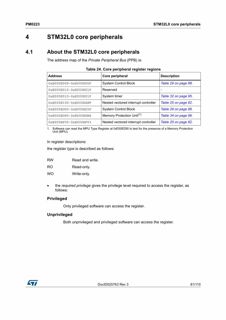
DocID025763 Rev 3 81/110
PM0223 STM32L0 core peripherals
108
4 STM32L0 core peripherals
4.1 About the STM32L0 core peripherals
The address map of the Private Peripheral Bus (PPB) is:
In register descriptions:
the register type is described as follows:
• the required privilege gives the privilege level required to access the register, as follows:
Privileged
Only privileged software can access the register.
Unprivileged
Both unprivileged and privileged software can access the register.
Table 24. Core peripheral register regions
Address Core peripheral Description
0xE000E008-0xE000E00F System Control Block Table 29 on page 88.
0xE000E010-0xE000E01F Reserved -
0xE000E010-0xE000E01F System timer Table 32 on page 95.
0xE000E100-0xE000E4EF Nested vectored interrupt controller Table 25 on page 82.
0xE000ED00-0xE000ED3F System Control Block Table 29 on page 88.
0xE000ED90-0xE000EDB8 Memory Protection Unit(1)
1. Software can read the MPU Type Register at 0xE000ED90 to test for the presence of a Memory Protection Unit (MPU).
Table 34 on page 99.
0xE000EF00-0xE000EF03 Nested vectored interrupt controller Table 25 on page 82.
RW Read and write.
RO Read-only.
WO Write-only.

STM32L0 core peripherals PM0223
82/110 DocID025763 Rev 3
4.2 Nested vectored interrupt controller
This section describes the Nested vectored interrupt controller (NVIC) and the registers it uses. The NVIC supports:
• 32 interrupts.
• A programmable priority level of 0-192 in steps of 64 for each interrupt. A higher level corresponds to a lower priority, so level 0 is the highest interrupt priority.
• Level and pulse detection of interrupt signals.
• Interrupt tail-chaining.
• An external Non-Maskable Interrupt (NMI).
The processor automatically stacks its state on exception entry and unstacks this state on exception exit, with no instruction overhead. This provides low latency exception handling. The hardware implementation of the NVIC registers is
:
4.2.1 Accessing the STM32L0 Cortex-M0+ NVIC registers using CMSIS
CMSIS functions enable software portability between different Cortex-M profile processors.
To access the NVIC registers when using CMSIS, use the following functions:
Table 25. NVIC register summary
Address Name Type Reset value Description
0xE000E100 NVIC_ISER RW 0x00000000Interrupt Set-enable Register on page 83.
0xE000E180 NVIC_ICER RW 0x00000000Interrupt Clear-enable Register on page 83.
0xE000E200 NVIC_ISPR RW 0x00000000Interrupt Set-pending Register on page 84.
0xE000E280 NVIC_ICPR RW 0x00000000Interrupt Clear-pending Register on page 84.
0xE000E400-0xE000E4EF NVIC_IPR0-7 RW 0x00000000Interrupt Priority Registers on page 85.
Table 26. CMSIS access NVIC functions
CMSIS function Description
void NVIC_EnableIRQ(IRQn_Type IRQn)(1) Enables an interrupt or exception.
void NVIC_DisableIRQ(IRQn_Type IRQn)(1) Disables an interrupt or exception.
void NVIC_SetPendingIRQ(IRQn_Type IRQn)(1)Sets the pending status of interrupt or exception to 1.
void NVIC_ClearPendingIRQ(IRQn_Type IRQn)(1)Clears the pending status of interrupt or exception to 0.
uint32_t NVIC_GetPendingIRQ(IRQn_Type IRQn)(1)Reads the pending status of interrupt or exception. This function returns non-zero value if the pending status is set to 1.
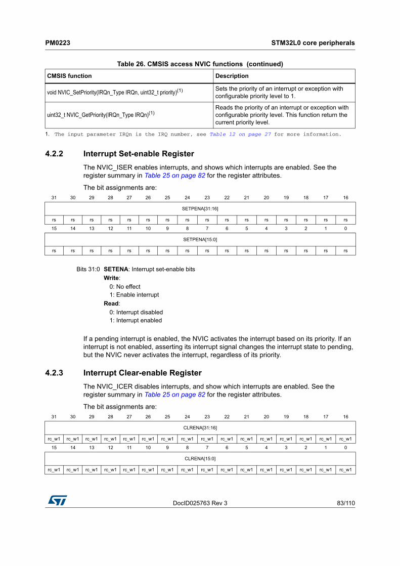
DocID025763 Rev 3 83/110
PM0223 STM32L0 core peripherals
108
4.2.2 Interrupt Set-enable Register
The NVIC_ISER enables interrupts, and shows which interrupts are enabled. See the register summary in Table 25 on page 82 for the register attributes.
The bit assignments are:
If a pending interrupt is enabled, the NVIC activates the interrupt based on its priority. If an interrupt is not enabled, asserting its interrupt signal changes the interrupt state to pending, but the NVIC never activates the interrupt, regardless of its priority.
4.2.3 Interrupt Clear-enable Register
The NVIC_ICER disables interrupts, and show which interrupts are enabled. See the register summary in Table 25 on page 82 for the register attributes.
The bit assignments are:
void NVIC_SetPriority(IRQn_Type IRQn, uint32_t priority)(1) Sets the priority of an interrupt or exception with configurable priority level to 1.
uint32_t NVIC_GetPriority(IRQn_Type IRQn)(1)Reads the priority of an interrupt or exception with configurable priority level. This function return the current priority level.
1. The input parameter IRQn is the IRQ number, see Table 12 on page 27 for more information.
Table 26. CMSIS access NVIC functions (continued)
CMSIS function Description
31 30 29 28 27 26 25 24 23 22 21 20 19 18 17 16
SETPENA[31:16]
rs rs rs rs rs rs rs rs rs rs rs rs rs rs rs rs
15 14 13 12 11 10 9 8 7 6 5 4 3 2 1 0
SETPENA[15:0]
rs rs rs rs rs rs rs rs rs rs rs rs rs rs rs rs
Bits 31:0 SETENA: Interrupt set-enable bits
Write:
0: No effect1: Enable interrupt
Read:
0: Interrupt disabled1: Interrupt enabled
31 30 29 28 27 26 25 24 23 22 21 20 19 18 17 16
CLRENA[31:16]
rc_w1 rc_w1 rc_w1 rc_w1 rc_w1 rc_w1 rc_w1 rc_w1 rc_w1 rc_w1 rc_w1 rc_w1 rc_w1 rc_w1 rc_w1 rc_w1
15 14 13 12 11 10 9 8 7 6 5 4 3 2 1 0
CLRENA[15:0]
rc_w1 rc_w1 rc_w1 rc_w1 rc_w1 rc_w1 rc_w1 rc_w1 rc_w1 rc_w1 rc_w1 rc_w1 rc_w1 rc_w1 rc_w1 rc_w1
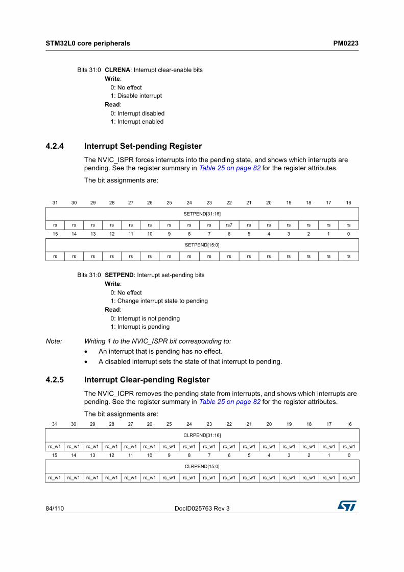
STM32L0 core peripherals PM0223
84/110 DocID025763 Rev 3
4.2.4 Interrupt Set-pending Register
The NVIC_ISPR forces interrupts into the pending state, and shows which interrupts are pending. See the register summary in Table 25 on page 82 for the register attributes.
The bit assignments are:
Note: Writing 1 to the NVIC_ISPR bit corresponding to:
• An interrupt that is pending has no effect.
• A disabled interrupt sets the state of that interrupt to pending.
4.2.5 Interrupt Clear-pending Register
The NVIC_ICPR removes the pending state from interrupts, and shows which interrupts are pending. See the register summary in Table 25 on page 82 for the register attributes.
The bit assignments are:
Bits 31:0 CLRENA: Interrupt clear-enable bits
Write:
0: No effect1: Disable interrupt
Read:
0: Interrupt disabled1: Interrupt enabled
31 30 29 28 27 26 25 24 23 22 21 20 19 18 17 16
SETPEND[31:16]
rs rs rs rs rs rs rs rs rs rs7 rs rs rs rs rs rs
15 14 13 12 11 10 9 8 7 6 5 4 3 2 1 0
SETPEND[15:0]
rs rs rs rs rs rs rs rs rs rs rs rs rs rs rs rs
Bits 31:0 SETPEND: Interrupt set-pending bits
Write:
0: No effect1: Change interrupt state to pending
Read:
0: Interrupt is not pending1: Interrupt is pending
31 30 29 28 27 26 25 24 23 22 21 20 19 18 17 16
CLRPEND[31:16]
rc_w1 rc_w1 rc_w1 rc_w1 rc_w1 rc_w1 rc_w1 rc_w1 rc_w1 rc_w1 rc_w1 rc_w1 rc_w1 rc_w1 rc_w1 rc_w1
15 14 13 12 11 10 9 8 7 6 5 4 3 2 1 0
CLRPEND[15:0]
rc_w1 rc_w1 rc_w1 rc_w1 rc_w1 rc_w1 rc_w1 rc_w1 rc_w1 rc_w1 rc_w1 rc_w1 rc_w1 rc_w1 rc_w1 rc_w1
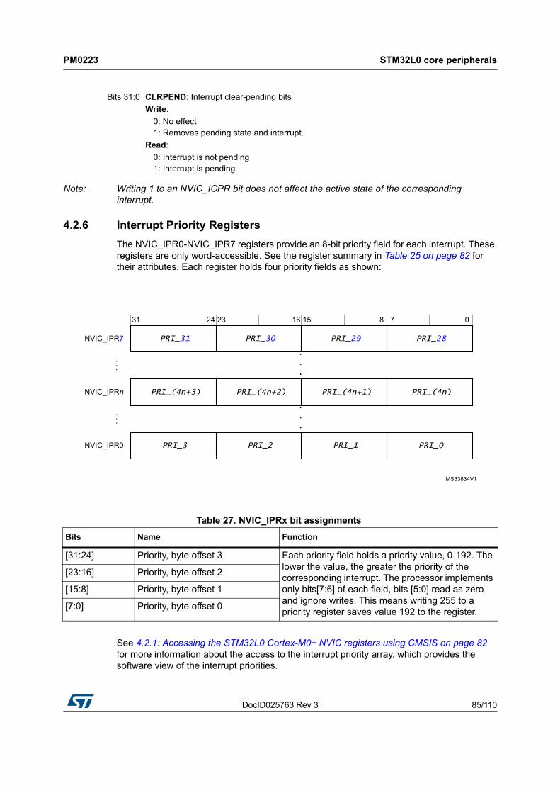
DocID025763 Rev 3 85/110
PM0223 STM32L0 core peripherals
108
Note: Writing 1 to an NVIC_ICPR bit does not affect the active state of the corresponding interrupt.
4.2.6 Interrupt Priority Registers
The NVIC_IPR0-NVIC_IPR7 registers provide an 8-bit priority field for each interrupt. These registers are only word-accessible. See the register summary in Table 25 on page 82 for their attributes. Each register holds four priority fields as shown:
See 4.2.1: Accessing the STM32L0 Cortex-M0+ NVIC registers using CMSIS on page 82 for more information about the access to the interrupt priority array, which provides the software view of the interrupt priorities.
Bits 31:0 CLRPEND: Interrupt clear-pending bits
Write:
0: No effect1: Removes pending state and interrupt.
Read:
0: Interrupt is not pending1: Interrupt is pending
Table 27. NVIC_IPRx bit assignments
Bits Name Function
[31:24] Priority, byte offset 3 Each priority field holds a priority value, 0-192. The lower the value, the greater the priority of the corresponding interrupt. The processor implements only bits[7:6] of each field, bits [5:0] read as zero and ignore writes. This means writing 255 to a priority register saves value 192 to the register.
[23:16] Priority, byte offset 2
[15:8] Priority, byte offset 1
[7:0] Priority, byte offset 0
STM32L0 core peripherals PM0223
86/110 DocID025763 Rev 3
Find the NVIC_IPR number and byte offset for interrupt M as follows:
• The corresponding NVIC_IPR number, N, is given by N = N DIV 4.
• The byte offset of the required Priority field in this register is M MOD 4, where:
– Byte offset 0 refers to register bits[7:0].
– Byte offset 1 refers to register bits[15:8].
– Byte offset 2 refers to register bits[23:16].
– Byte offset 3 refers to register bits[31:24].
4.2.7 Level-sensitive and pulse interrupts
STM32L0 interrupts are both level-sensitive and pulse-sensitive. Pulse interrupts are also described as edge-triggered interrupts.
A level-sensitive interrupt is held asserted until the peripheral deasserts the interrupt signal. Typically this happens because the ISR accesses the peripheral, causing it to clear the interrupt request. A pulse interrupt is an interrupt signal sampled synchronously on the rising edge of the processor clock. To ensure the NVIC detects the interrupt, the peripheral must assert the interrupt signal for at least one clock cycle, during which the NVIC detects the pulse and latches the interrupt.
When the processor enters the ISR, it automatically removes the pending state from the interrupt, see Hardware and software control of interrupts on page 86. For a level-sensitive interrupt, if the signal is not deasserted before the processor returns from the ISR, the interrupt becomes pending again, and the processor must execute its ISR again. This means that the peripheral can hold the interrupt signal asserted until it no longer requires servicing.
Hardware and software control of interrupts
The STM32L0 Cortex-M0+ latches all interrupts. A peripheral interrupt becomes pending for one of the following reasons:
• The NVIC detects that the interrupt signal is active and the corresponding interrupt is not active.
• The NVIC detects a rising edge on the interrupt signal.
• Software writes to the corresponding interrupt set-pending register bit, see 4.2.4: Interrupt Set-pending Register on page 84.
A pending interrupt remains pending until one of the following:
• The processor enters the ISR for the interrupt. This changes the state of the interrupt from pending to active. Then:
– For a level-sensitive interrupt, when the processor returns from the ISR, the NVIC samples the interrupt signal. If the signal is asserted, the state of the interrupt changes to pending, which might cause the processor to immediately re-enter the ISR. Otherwise, the state of the interrupt changes to inactive.
– For a pulse interrupt, the NVIC continues to monitor the interrupt signal, and if this is pulsed the state of the interrupt changes to pending and active. In this case, when the processor returns from the ISR the state of the interrupt changes to pending, which might cause the processor to immediately re-enter the ISR. If the interrupt signal is not pulsed while the processor is in the ISR, when the processor returns from the ISR the state of the interrupt changes to inactive.
• Software writes to the corresponding interrupt clear-pending register bit.
DocID025763 Rev 3 87/110
PM0223 STM32L0 core peripherals
108
For a level-sensitive interrupt, if the interrupt signal is still asserted, the state of the interrupt does not change. Otherwise, the state of the interrupt changes to inactive.
For a pulse interrupt, state of the interrupt changes to:
– Inactive, if the state was pending.
– Active, if the state was active and pending.
4.2.8 NVIC usage hints and tips
Ensure software uses correctly aligned register accesses. The processor does not support unaligned accesses to NVIC registers.
An interrupt can enter pending state even if it is disabled. Disabling an interrupt only prevents the processor from taking that interrupt.
Before programming VTOR to relocate the vector table, ensure the vector table entries of the new vector table are set up for fault handlers, NMI and all enabled exception like interrupts. For more information, see 4.3.4: Vector Table Offset Register on page 91.
NVIC programming hints
Software uses the CPSIE i and CPSIDi instructions to enable and disable interrupts. The CMSIS provides the following intrinsic functions for these instructions:
void __disable_irq(void) // Disable Interrupts void __enable_irq(void) // Enable Interrupts
In addition, the CMSIS provides a number of functions for NVIC control, including:
The input parameter IRQn is the IRQ number, see Table 12 on page 27 for more information. For more information about these functions, see the CMSIS documentation.
Table 28. CMSIS functions for NVIC control
CMSIS interrupt control function Description
void NVIC_EnableIRQ(IRQn_t IRQn) Enable IRQn.
void NVIC_DisableIRQ(IRQn_t IRQn) Disable IRQn
uint32_t NVIC_GetPendingIRQ (IRQn_t IRQn) Return true (1) if IRQn is pending.
void NVIC_SetPendingIRQ (IRQn_t IRQn) Set IRQn pending.
void NVIC_ClearPendingIRQ (IRQn_t IRQn) Clear IRQn pending status.
void NVIC_SetPriority (IRQn_t IRQn, uint32_t priority)
Set priority for IRQn.
uint32_t NVIC_GetPriority (IRQn_t IRQn) Read priority of IRQn.
void NVIC_SystemReset (void) Reset the system.
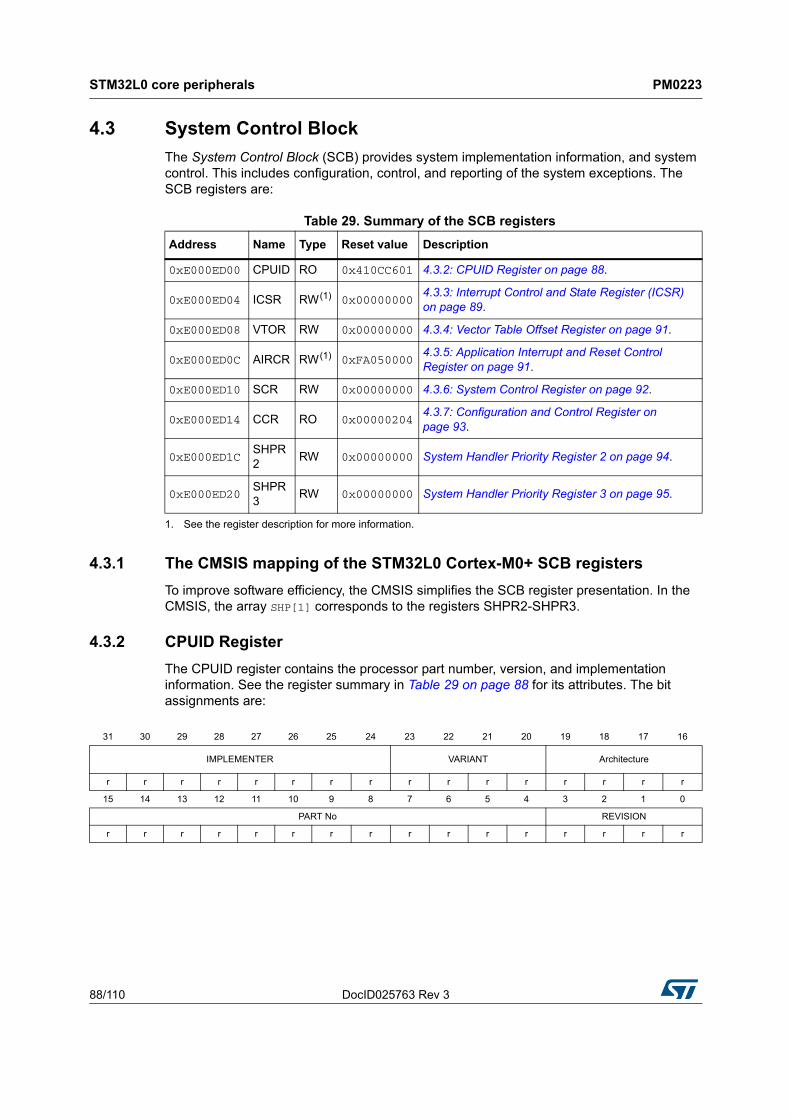
STM32L0 core peripherals PM0223
88/110 DocID025763 Rev 3
4.3 System Control Block
The System Control Block (SCB) provides system implementation information, and system control. This includes configuration, control, and reporting of the system exceptions. The SCB registers are:
4.3.1 The CMSIS mapping of the STM32L0 Cortex-M0+ SCB registers
To improve software efficiency, the CMSIS simplifies the SCB register presentation. In the CMSIS, the array SHP[1] corresponds to the registers SHPR2-SHPR3.
4.3.2 CPUID Register
The CPUID register contains the processor part number, version, and implementation information. See the register summary in Table 29 on page 88 for its attributes. The bit assignments are:
Table 29. Summary of the SCB registers
Address Name Type Reset value Description
0xE000ED00 CPUID RO 0x410CC601 4.3.2: CPUID Register on page 88.
0xE000ED04 ICSR RW (1)
1. See the register description for more information.
0x000000004.3.3: Interrupt Control and State Register (ICSR) on page 89.
0xE000ED08 VTOR RW 0x00000000 4.3.4: Vector Table Offset Register on page 91.
0xE000ED0C AIRCR RW (1) 0xFA0500004.3.5: Application Interrupt and Reset Control Register on page 91.
0xE000ED10 SCR RW 0x00000000 4.3.6: System Control Register on page 92.
0xE000ED14 CCR RO 0x000002044.3.7: Configuration and Control Register on page 93.
0xE000ED1CSHPR2
RW 0x00000000 System Handler Priority Register 2 on page 94.
0xE000ED20SHPR3
RW 0x00000000 System Handler Priority Register 3 on page 95.
31 30 29 28 27 26 25 24 23 22 21 20 19 18 17 16
IMPLEMENTER VARIANT Architecture
r r r r r r r r r r r r r r r r
15 14 13 12 11 10 9 8 7 6 5 4 3 2 1 0
PART No REVISION
r r r r r r r r r r r r r r r r
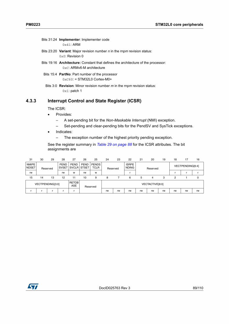
DocID025763 Rev 3 89/110
PM0223 STM32L0 core peripherals
108
4.3.3 Interrupt Control and State Register (ICSR)
The ICSR:
• Provides:
– A set-pending bit for the Non-Maskable Interrupt (NMI) exception.
– Set-pending and clear-pending bits for the PendSV and SysTick exceptions.
• Indicates:
– The exception number of the highest priority pending exception.
See the register summary in Table 29 on page 88 for the ICSR attributes. The bit assignments are
Bits 31:24 Implementer: Implementer code
0x41: ARM
Bits 23:20 Variant: Major revision number n in the rnpm revision status:
0x0: Revision 0
Bits 19:16 Architecture: Constant that defines the architecture of the processor:
0xC: ARMv6-M architecture
Bits 15:4 PartNo: Part number of the processor
0xC60: = STM32L0 Cortex-M0+
Bits 3:0 Revision: Minor revision number m in the rnpm revision status:
0x1: patch 1
31 30 29 28 27 26 25 24 23 22 21 20 19 18 17 16
NMIPENDSET Reserved
PENDSVSET
PENDSVCLR
PENDSTSET
PENDSTCLR Reserved
ISRPENDING Reserved
VECTPENDING[6:4]
rw rw w rw w r r r r
15 14 13 12 11 10 9 8 7 6 5 4 3 2 1 0
VECTPENDING[3:0] RETOBASE Reserved
VECTACTIVE[8:0]
r r r r r rw rw rw rw rw rw rw rw rw
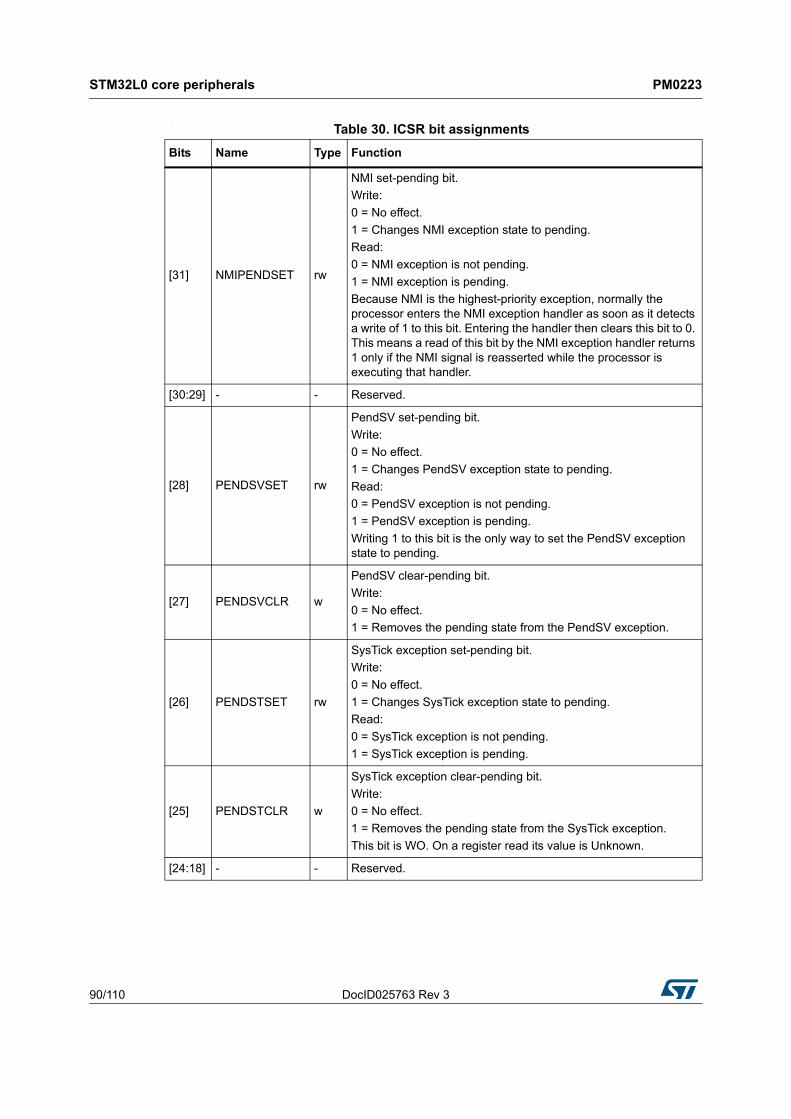
STM32L0 core peripherals PM0223
90/110 DocID025763 Rev 3
:
Table 30. ICSR bit assignments
Bits Name Type Function
[31] NMIPENDSET rw
NMI set-pending bit.
Write:
0 = No effect.
1 = Changes NMI exception state to pending.
Read:
0 = NMI exception is not pending.
1 = NMI exception is pending.
Because NMI is the highest-priority exception, normally the processor enters the NMI exception handler as soon as it detects a write of 1 to this bit. Entering the handler then clears this bit to 0. This means a read of this bit by the NMI exception handler returns 1 only if the NMI signal is reasserted while the processor is executing that handler.
[30:29] - - Reserved.
[28] PENDSVSET rw
PendSV set-pending bit.
Write:
0 = No effect.
1 = Changes PendSV exception state to pending.
Read:
0 = PendSV exception is not pending.
1 = PendSV exception is pending.
Writing 1 to this bit is the only way to set the PendSV exception state to pending.
[27] PENDSVCLR w
PendSV clear-pending bit.
Write:
0 = No effect.
1 = Removes the pending state from the PendSV exception.
[26] PENDSTSET rw
SysTick exception set-pending bit.
Write:
0 = No effect.
1 = Changes SysTick exception state to pending.
Read:
0 = SysTick exception is not pending.
1 = SysTick exception is pending.
[25] PENDSTCLR w
SysTick exception clear-pending bit.
Write:
0 = No effect.
1 = Removes the pending state from the SysTick exception.
This bit is WO. On a register read its value is Unknown.
[24:18] - - Reserved.
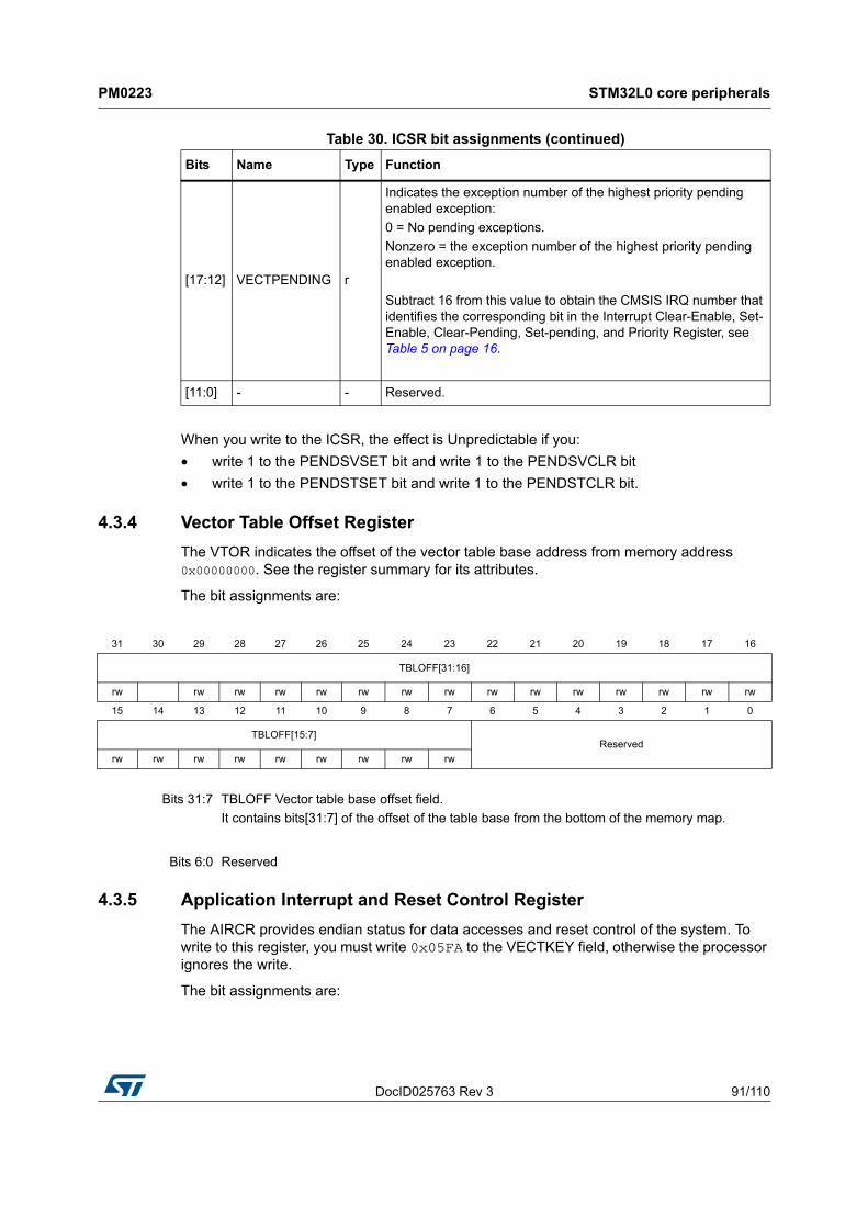
DocID025763 Rev 3 91/110
PM0223 STM32L0 core peripherals
108
When you write to the ICSR, the effect is Unpredictable if you:
• write 1 to the PENDSVSET bit and write 1 to the PENDSVCLR bit
• write 1 to the PENDSTSET bit and write 1 to the PENDSTCLR bit.
4.3.4 Vector Table Offset Register
The VTOR indicates the offset of the vector table base address from memory address 0x00000000. See the register summary for its attributes.
The bit assignments are:
4.3.5 Application Interrupt and Reset Control Register
The AIRCR provides endian status for data accesses and reset control of the system. To write to this register, you must write 0x05FA to the VECTKEY field, otherwise the processor ignores the write.
The bit assignments are:
[17:12] VECTPENDING r
Indicates the exception number of the highest priority pending enabled exception:
0 = No pending exceptions.
Nonzero = the exception number of the highest priority pending enabled exception.
Subtract 16 from this value to obtain the CMSIS IRQ number that identifies the corresponding bit in the Interrupt Clear-Enable, Set-Enable, Clear-Pending, Set-pending, and Priority Register, see Table 5 on page 16.
[11:0] - - Reserved.
Table 30. ICSR bit assignments (continued)
Bits Name Type Function
31 30 29 28 27 26 25 24 23 22 21 20 19 18 17 16
TBLOFF[31:16]
rw rw rw rw rw rw rw rw rw rw rw rw rw rw rw
15 14 13 12 11 10 9 8 7 6 5 4 3 2 1 0
TBLOFF[15:7]Reserved
rw rw rw rw rw rw rw rw rw
Bits 31:7 TBLOFF Vector table base offset field.
It contains bits[31:7] of the offset of the table base from the bottom of the memory map.
Bits 6:0 Reserved
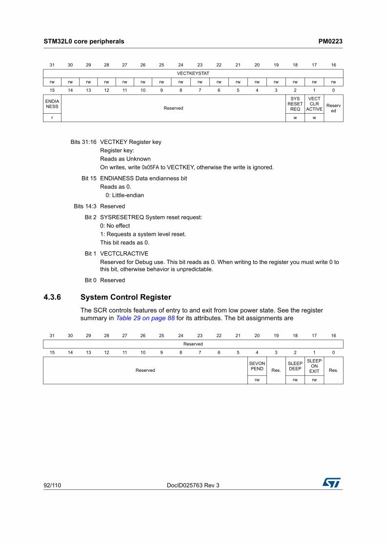
STM32L0 core peripherals PM0223
92/110 DocID025763 Rev 3
4.3.6 System Control Register
The SCR controls features of entry to and exit from low power state. See the register summary in Table 29 on page 88 for its attributes. The bit assignments are
31 30 29 28 27 26 25 24 23 22 21 20 19 18 17 16
VECTKEYSTAT
rw rw rw rw rw rw rw rw rw rw rw rw rw rw rw rw
15 14 13 12 11 10 9 8 7 6 5 4 3 2 1 0
ENDIANESS Reserved
SYS RESET
REQ
VECT CLR
ACTIVEReserv
ed
r w w
Bits 31:16 VECTKEY Register key
Register key:
Reads as Unknown
On writes, write 0x05FA to VECTKEY, otherwise the write is ignored.
Bit 15 ENDIANESS Data endianness bit
Reads as 0.
0: Little-endian
Bits 14:3 Reserved
Bit 2 SYSRESETREQ System reset request:
0: No effect
1: Requests a system level reset.
This bit reads as 0.
Bit 1 VECTCLRACTIVE
Reserved for Debug use. This bit reads as 0. When writing to the register you must write 0 to this bit, otherwise behavior is unpredictable.
Bit 0 Reserved
31 30 29 28 27 26 25 24 23 22 21 20 19 18 17 16
Reserved
15 14 13 12 11 10 9 8 7 6 5 4 3 2 1 0
Reserved
SEVONPEND Res.
SLEEPDEEP
SLEEP ON
EXIT Res.
rw rw rw
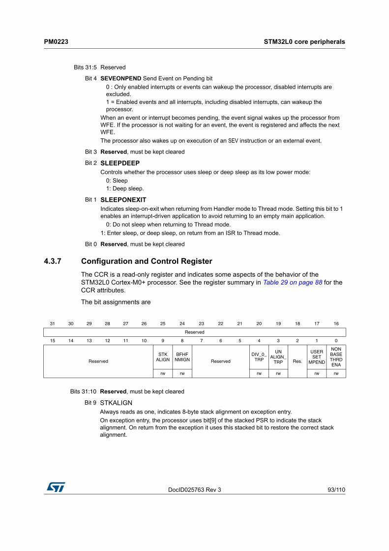
DocID025763 Rev 3 93/110
PM0223 STM32L0 core peripherals
108
4.3.7 Configuration and Control Register
The CCR is a read-only register and indicates some aspects of the behavior of the STM32L0 Cortex-M0+ processor. See the register summary in Table 29 on page 88 for the CCR attributes.
The bit assignments are
Bits 31:5 Reserved
Bit 4 SEVEONPEND Send Event on Pending bit
0 : Only enabled interrupts or events can wakeup the processor, disabled interrupts are excluded.1 = Enabled events and all interrupts, including disabled interrupts, can wakeup the processor.
When an event or interrupt becomes pending, the event signal wakes up the processor from WFE. If the processor is not waiting for an event, the event is registered and affects the next WFE.
The processor also wakes up on execution of an SEV instruction or an external event.
Bit 3 Reserved, must be kept cleared
Bit 2 SLEEPDEEP Controls whether the processor uses sleep or deep sleep as its low power mode:
0: Sleep1: Deep sleep.
Bit 1 SLEEPONEXIT Indicates sleep-on-exit when returning from Handler mode to Thread mode. Setting this bit to 1 enables an interrupt-driven application to avoid returning to an empty main application.
0: Do not sleep when returning to Thread mode.
1: Enter sleep, or deep sleep, on return from an ISR to Thread mode.
Bit 0 Reserved, must be kept cleared
31 30 29 28 27 26 25 24 23 22 21 20 19 18 17 16
Reserved
15 14 13 12 11 10 9 8 7 6 5 4 3 2 1 0
Reserved
STK ALIGN
BFHF NMIGN Reserved
DIV_0_TRP
UN ALIGN_
TRP Res.
USER SET
MPEND
NON BASE THRD ENA
rw rw rw rw rw rw
Bits 31:10 Reserved, must be kept cleared
Bit 9 STKALIGNAlways reads as one, indicates 8-byte stack alignment on exception entry.
On exception entry, the processor uses bit[9] of the stacked PSR to indicate the stack alignment. On return from the exception it uses this stacked bit to restore the correct stack alignment.
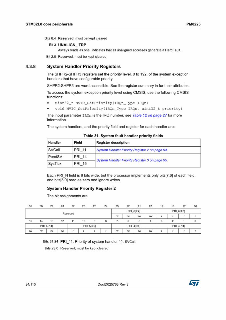
STM32L0 core peripherals PM0223
94/110 DocID025763 Rev 3
4.3.8 System Handler Priority Registers
The SHPR2-SHPR3 registers set the priority level, 0 to 192, of the system exception handlers that have configurable priority.
SHPR2-SHPR3 are word accessible. See the register summary in for their attributes.
To access the system exception priority level using CMSIS, use the following CMSIS functions:
• uint32_t NVIC_GetPriority(IRQn_Type IRQn)
• void NVIC_SetPriority(IRQn_Type IRQn, uint32_t priority)
The input parameter IRQn is the IRQ number, see Table 12 on page 27 for more information.
The system handlers, and the priority field and register for each handler are:
Each PRI_N field is 8 bits wide, but the processor implements only bits[7:6] of each field, and bits[5:0] read as zero and ignore writes.
System Handler Priority Register 2
The bit assignments are:
Bits 8:4 Reserved, must be kept cleared
Bit 3 UNALIGN_ TRP Always reads as one, indicates that all unaligned accesses generate a HardFault.
Bit 2:0 Reserved, must be kept cleared
Table 31. System fault handler priority fields
Handler Field Register description
SVCall PRI_11 System Handler Priority Register 2 on page 94.
PendSV PRI_14System Handler Priority Register 3 on page 95.
SysTick PRI_15
31 30 29 28 27 26 25 24 23 22 21 20 19 18 17 16
ReservedPRI_6[7:4] PRI_6[3:0]
rw rw rw rw r r r r
15 14 13 12 11 10 9 8 7 6 5 4 3 2 1 0
PRI_5[7:4] PRI_5[3:0] PRI_4[7:4] PRI_4[7:4]
rw rw rw rw r r r r rw rw rw rw r r r r
Bits 31:24 PRI_11: Priority of system handler 11, SVCall.
Bits 23:0 Reserved, must be kept cleared
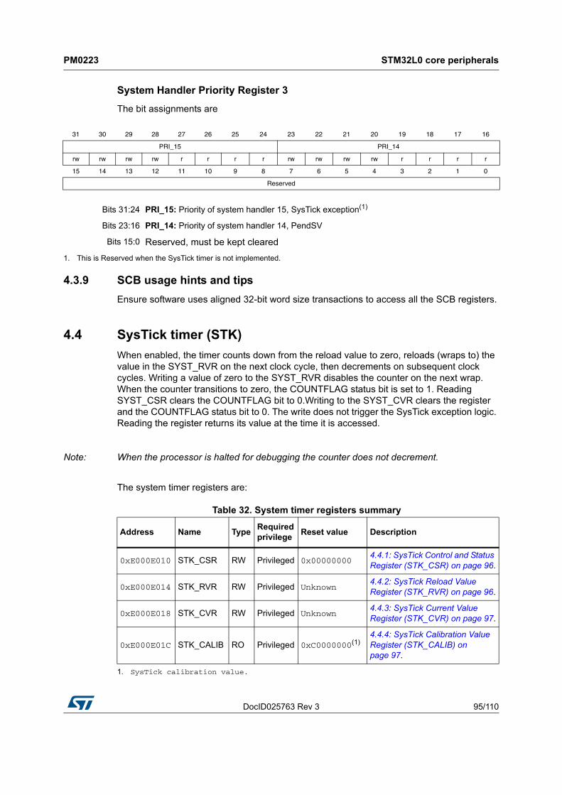
DocID025763 Rev 3 95/110
PM0223 STM32L0 core peripherals
108
System Handler Priority Register 3
The bit assignments are
4.3.9 SCB usage hints and tips
Ensure software uses aligned 32-bit word size transactions to access all the SCB registers.
4.4 SysTick timer (STK)
When enabled, the timer counts down from the reload value to zero, reloads (wraps to) the value in the SYST_RVR on the next clock cycle, then decrements on subsequent clock cycles. Writing a value of zero to the SYST_RVR disables the counter on the next wrap. When the counter transitions to zero, the COUNTFLAG status bit is set to 1. Reading SYST_CSR clears the COUNTFLAG bit to 0.Writing to the SYST_CVR clears the register and the COUNTFLAG status bit to 0. The write does not trigger the SysTick exception logic. Reading the register returns its value at the time it is accessed.
Note: When the processor is halted for debugging the counter does not decrement.
The system timer registers are:
31 30 29 28 27 26 25 24 23 22 21 20 19 18 17 16
PRI_15 PRI_14
rw rw rw rw r r r r rw rw rw rw r r r r
15 14 13 12 11 10 9 8 7 6 5 4 3 2 1 0
Reserved
Bits 31:24 PRI_15: Priority of system handler 15, SysTick exception(1)
Bits 23:16 PRI_14: Priority of system handler 14, PendSV
Bits 15:0 Reserved, must be kept cleared
1. This is Reserved when the SysTick timer is not implemented.
Table 32. System timer registers summary
Address Name TypeRequired privilege
Reset value Description
0xE000E010 STK_CSR RW Privileged 0x000000004.4.1: SysTick Control and Status Register (STK_CSR) on page 96.
0xE000E014 STK_RVR RW Privileged Unknown4.4.2: SysTick Reload Value Register (STK_RVR) on page 96.
0xE000E018 STK_CVR RW Privileged Unknown4.4.3: SysTick Current Value Register (STK_CVR) on page 97.
0xE000E01C STK_CALIB RO Privileged 0xC0000000(1)
1. SysTick calibration value.
4.4.4: SysTick Calibration Value Register (STK_CALIB) on page 97.
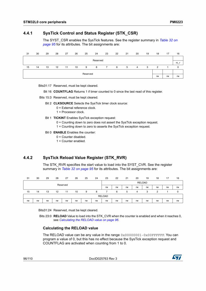
STM32L0 core peripherals PM0223
96/110 DocID025763 Rev 3
4.4.1 SysTick Control and Status Register (STK_CSR)
The SYST_CSR enables the SysTick features. See the register summary in Table 32 on page 95 for its attributes. The bit assignments are:
4.4.2 SysTick Reload Value Register (STK_RVR)
The STK_RVR specifies the start value to load into the SYST_CVR. See the register summary in Table 32 on page 95 for its attributes. The bit assignments are:
Calculating the RELOAD value
The RELOAD value can be any value in the range 0x00000001-0x00FFFFFF. You can program a value of 0, but this has no effect because the SysTick exception request and COUNTFLAG are activated when counting from 1 to 0.
31 30 29 28 27 26 25 24 23 22 21 20 19 18 17 16
Reservedrc_r
15 14 13 12 11 10 9 8 7 6 5 4 3 2 1 0
Reservedrw rw rw
Bits31:17 Reserved, must be kept cleared.
Bit 16 COUNTFLAG Returns 1 if timer counted to 0 since the last read of this register.
Bits 15:3 Reserved, must be kept cleared.
Bit 2 CLKSOURCE Selects the SysTick timer clock source:
0 = External reference clock.1 = Processor clock.
Bit 1 TICKINT Enables SysTick exception request:
0 = Counting down to zero does not assert the SysTick exception request.1 = Counting down to zero to asserts the SysTick exception request.
Bit 0 ENABLE Enables the counter:
0 = Counter disabled.1 = Counter enabled.
31 30 29 28 27 26 25 24 23 22 21 20 19 18 17 16
ReservedRELOAD
rw rw rw rw rw rw rw rw
15 14 13 12 11 10 9 8 7 6 5 4 3 2 1 0
RELOAD
rw rw rw rw rw rw rw rw rw rw rw rw rw rw rw rw
Bits31:24 Reserved, must be kept cleared.
Bits 23:0 RELOAD Value to load into the STK_CVR when the counter is enabled and when it reaches 0, see Calculating the RELOAD value on page 96.
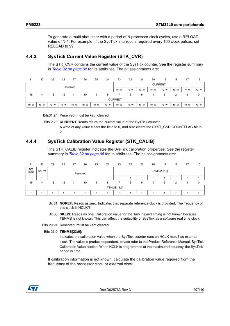
DocID025763 Rev 3 97/110
PM0223 STM32L0 core peripherals
108
To generate a multi-shot timer with a period of N processor clock cycles, use a RELOAD value of N-1. For example, if the SysTick interrupt is required every 100 clock pulses, set RELOAD to 99.
4.4.3 SysTick Current Value Register (STK_CVR)
The STK_CVR contains the current value of the SysTick counter. See the register summary in Table 32 on page 95 for its attributes. The bit assignments are:
4.4.4 SysTick Calibration Value Register (STK_CALIB)
The STK_CALIB register indicates the SysTick calibration properties. See the register summary in Table 32 on page 95 for its attributes. The bit assignments are:
If calibration information is not known, calculate the calibration value required from the frequency of the processor clock or external clock.
31 30 29 28 27 26 25 24 23 22 21 20 19 18 17 16
ReservedCURRENT
rc_w rc_w rc_w rc_w rc_w rc_w rc_w rc_w
15 14 13 12 11 10 9 8 7 6 5 4 3 2 1 0
CURRENT
rc_w rc_w rc_w rc_w rc_w rc_w rc_w rc_w rc_w rc_w rc_w rc_w rc_w rc_w rc_w rc_w
Bits31:24 Reserved, must be kept cleared.
Bits 23:0 CURRENT Reads return the current value of the SysTick counter.
A write of any value clears the field to 0, and also clears the SYST_CSR.COUNTFLAG bit to 0.
31 30 29 28 27 26 25 24 23 22 21 20 19 18 17 16
NO REF SKEW
ReservedTENMS[23:16]
r r r r r r r r r r
15 14 13 12 11 10 9 8 7 6 5 4 3 2 1 0
TENMS[15:0]
r r r r r r r r r r r r r r r r
Bit 31 NOREF: Reads as zero. Indicates that separate reference clock is provided. The frequency of this clock is HCLK/8.
Bit 30 SKEW: Reads as one. Calibration value for the 1ms inexact timing is not known because TENMS is not known. This can affect the suitability of SysTick as a software real time clock.
Bits 29:24 Reserved, must be kept cleared.
Bits 23:0 TENMS[23:0]:
Indicates the calibration value when the SysTick counter runs on HCLK max/8 as external
clock. The value is product dependent, please refer to the Product Reference Manual, SysTick
Calibration Value section. When HCLK is programmed at the maximum frequency, the SysTick period is 1ms.
STM32L0 core peripherals PM0223
98/110 DocID025763 Rev 3
4.4.5 SysTick usage hints and tips
The interrupt controller clock updates the SysTick counter. If this clock signal is stopped for low power mode, the SysTick counter stops.
Ensure software uses word accesses to access the SysTick registers.
If the SysTick counter reload and current value are undefined at reset, the correct initialization sequence for the SysTick counter is:
1. Program reload value.
2. Clear current value.
3. Program Control and Status register.
4.5 Memory Protection Unit
This section describes the Memory Protection Unit (MPU).
The MPU can divide the memory map into a number of regions, and defines the location, size, access permissions, and memory attributes of each region. It supports:
• Independent attribute settings for each region.
• Overlapping regions.
• Export of memory attributes to the system.
The memory attributes affect the behavior of memory accesses to the region. The STM32L0 Cortex-M0+ MPU defines:
• Eight separate memory regions, 0-7.
• A background region.
When memory regions overlap, a memory access is affected by the attributes of the region with the highest number. For example, the attributes for region 7 take precedence over the attributes of any region that overlaps region 7.
The background region has the same memory access attributes as the default memory map, but is accessible from privileged software only.
The STM32L0 Cortex-M0+ MPU memory map is unified. This means instruction accesses and data accesses have same region settings.
If a program accesses a memory location that is prohibited by the MPU, the processor generates a HardFault exception.
In an OS environment, the kernel can update the MPU region setting dynamically based on the process to be executed. Typically, an embedded OS uses the MPU for memory protection.
Configuration of MPU regions is based on memory types, see 2.2.1: Memory regions, types and attributes on page 21.
Table 33 on page 99 shows the possible MPU region attributes. These include Shareability and cache behavior attributes that are not relevant to most microcontroller implementations. See MPU configuration for a microcontroller on page 107 for guidelines for programming such an implementation.
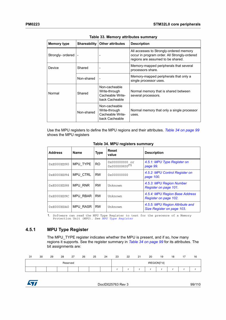
DocID025763 Rev 3 99/110
PM0223 STM32L0 core peripherals
108
Use the MPU registers to define the MPU regions and their attributes. Table 34 on page 99 shows the MPU registers
4.5.1 MPU Type Register
The MPU_TYPE register indicates whether the MPU is present, and if so, how many regions it supports. See the register summary in Table 34 on page 99 for its attributes. The bit assignments are:
Table 33. Memory attributes summary
Memory type Shareability Other attributes Description
Strongly- ordered - -All accesses to Strongly-ordered memory occur in program order. All Strongly-ordered regions are assumed to be shared.
Device Shared -Memory-mapped peripherals that several processors share.
Non-shared -Memory-mapped peripherals that only a single processor uses.
Normal Shared
Non-cacheable Write-through Cacheable Write-back Cacheable
Normal memory that is shared between several processors.
Non-shared
Non-cacheable Write-through Cacheable Write-back Cacheable
Normal memory that only a single processor uses.
Table 34. MPU registers summary
Address Name TypeReset value
Description
0xE000ED90 MPU_TYPE RO0x00000000 or 0x00000800(1)
1. Software can read the MPU Type Register to test for the precence of a Memory Protection Unit (MPU). See MPU Type Register
4.5.1: MPU Type Register on page 99.
0xE000ED94 MPU_CTRL RW 0x000000004.5.2: MPU Control Register on page 100.
0xE000ED98 MPU_RNR RW Unknown4.5.3: MPU Region Number Register on page 101.
0xE000ED9C MPU_RBAR RW Unknown4.5.4: MPU Region Base Address Register on page 102.
0xE000EDA0 MPU_RASR RW Unknown4.5.5: MPU Region Attribute and Size Register on page 103.
31 30 29 28 27 26 25 24 23 22 21 20 19 18 17 16
Reserved IREGION[7:0]
r r r r r r r r
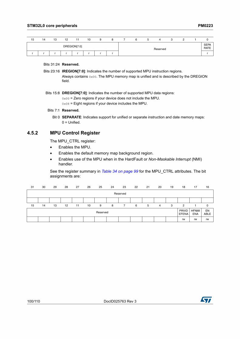
STM32L0 core peripherals PM0223
100/110 DocID025763 Rev 3
4.5.2 MPU Control Register
The MPU_CTRL register:
• Enables the MPU.
• Enables the default memory map background region.
• Enables use of the MPU when in the HardFault or Non-Maskable Interrupt (NMI) handler.
See the register summary in Table 34 on page 99 for the MPU_CTRL attributes. The bit assignments are:
15 14 13 12 11 10 9 8 7 6 5 4 3 2 1 0
DREGION[7:0]Reserved
SEPA RATE
r r r r r r r r r
Bits 31:24 Reserved.
Bits 23:16 IREGION[7:0]: Indicates the number of supported MPU instruction regions.
Always contains 0x00. The MPU memory map is unified and is described by the DREGION field.
Bits 15:8 DREGION[7:0]: Indicates the number of supported MPU data regions:
0x00 = Zero regions if your device does not include the MPU.
0x08 = Eight regions if your device includes the MPU.
Bits 7:1 Reserved.
Bit 0 SEPARATE: Indicates support for unified or separate instruction and date memory maps:
0 = Unified.
31 30 29 28 27 26 25 24 23 22 21 20 19 18 17 16
Reserved
15 14 13 12 11 10 9 8 7 6 5 4 3 2 1 0
Reserved PRIVDEFENA
HFNMIENA
EN ABLE
rw rw rw
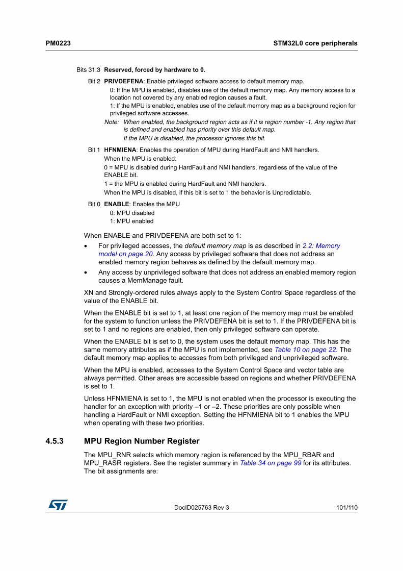
DocID025763 Rev 3 101/110
PM0223 STM32L0 core peripherals
108
When ENABLE and PRIVDEFENA are both set to 1:
• For privileged accesses, the default memory map is as described in 2.2: Memory model on page 20. Any access by privileged software that does not address an enabled memory region behaves as defined by the default memory map.
• Any access by unprivileged software that does not address an enabled memory region causes a MemManage fault.
XN and Strongly-ordered rules always apply to the System Control Space regardless of the value of the ENABLE bit.
When the ENABLE bit is set to 1, at least one region of the memory map must be enabled for the system to function unless the PRIVDEFENA bit is set to 1. If the PRIVDEFENA bit is set to 1 and no regions are enabled, then only privileged software can operate.
When the ENABLE bit is set to 0, the system uses the default memory map. This has the same memory attributes as if the MPU is not implemented, see Table 10 on page 22. The default memory map applies to accesses from both privileged and unprivileged software.
When the MPU is enabled, accesses to the System Control Space and vector table are always permitted. Other areas are accessible based on regions and whether PRIVDEFENA is set to 1.
Unless HFNMIENA is set to 1, the MPU is not enabled when the processor is executing the handler for an exception with priority –1 or –2. These priorities are only possible when handling a HardFault or NMI exception. Setting the HFNMIENA bit to 1 enables the MPU when operating with these two priorities.
4.5.3 MPU Region Number Register
The MPU_RNR selects which memory region is referenced by the MPU_RBAR and MPU_RASR registers. See the register summary in Table 34 on page 99 for its attributes. The bit assignments are:
Bits 31:3 Reserved, forced by hardware to 0.
Bit 2 PRIVDEFENA: Enable privileged software access to default memory map.
0: If the MPU is enabled, disables use of the default memory map. Any memory access to a location not covered by any enabled region causes a fault.1: If the MPU is enabled, enables use of the default memory map as a background region for privileged software accesses.
Note: When enabled, the background region acts as if it is region number -1. Any region that is defined and enabled has priority over this default map. If the MPU is disabled, the processor ignores this bit.
Bit 1 HFNMIENA: Enables the operation of MPU during HardFault and NMI handlers.
When the MPU is enabled:
0 = MPU is disabled during HardFault and NMI handlers, regardless of the value of the ENABLE bit.
1 = the MPU is enabled during HardFault and NMI handlers.
When the MPU is disabled, if this bit is set to 1 the behavior is Unpredictable.
Bit 0 ENABLE: Enables the MPU
0: MPU disabled1: MPU enabled
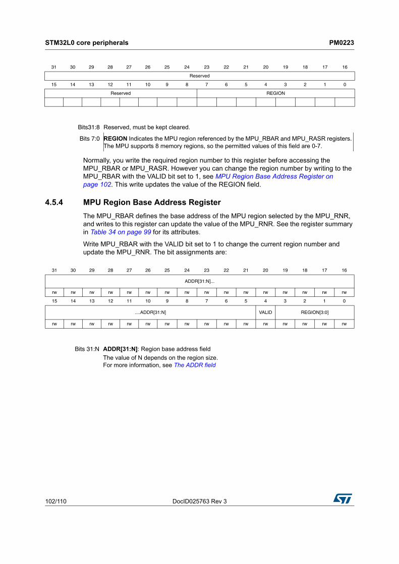
STM32L0 core peripherals PM0223
102/110 DocID025763 Rev 3
Normally, you write the required region number to this register before accessing the MPU_RBAR or MPU_RASR. However you can change the region number by writing to the MPU_RBAR with the VALID bit set to 1, see MPU Region Base Address Register on page 102. This write updates the value of the REGION field.
4.5.4 MPU Region Base Address Register
The MPU_RBAR defines the base address of the MPU region selected by the MPU_RNR, and writes to this register can update the value of the MPU_RNR. See the register summary in Table 34 on page 99 for its attributes.
Write MPU_RBAR with the VALID bit set to 1 to change the current region number and update the MPU_RNR. The bit assignments are:
31 30 29 28 27 26 25 24 23 22 21 20 19 18 17 16
Reserved
15 14 13 12 11 10 9 8 7 6 5 4 3 2 1 0
Reserved REGION
Bits31:8 Reserved, must be kept cleared.
Bits 7:0 REGION Indicates the MPU region referenced by the MPU_RBAR and MPU_RASR registers. The MPU supports 8 memory regions, so the permitted values of this field are 0-7.
31 30 29 28 27 26 25 24 23 22 21 20 19 18 17 16
ADDR[31:N]...
rw rw rw rw rw rw rw rw rw rw rw rw rw rw rw rw
15 14 13 12 11 10 9 8 7 6 5 4 3 2 1 0
....ADDR[31:N] VALID REGION[3:0]
rw rw rw rw rw rw rw rw rw rw rw rw rw rw rw rw
Bits 31:N ADDR[31:N]: Region base address field
The value of N depends on the region size. For more information, see The ADDR field
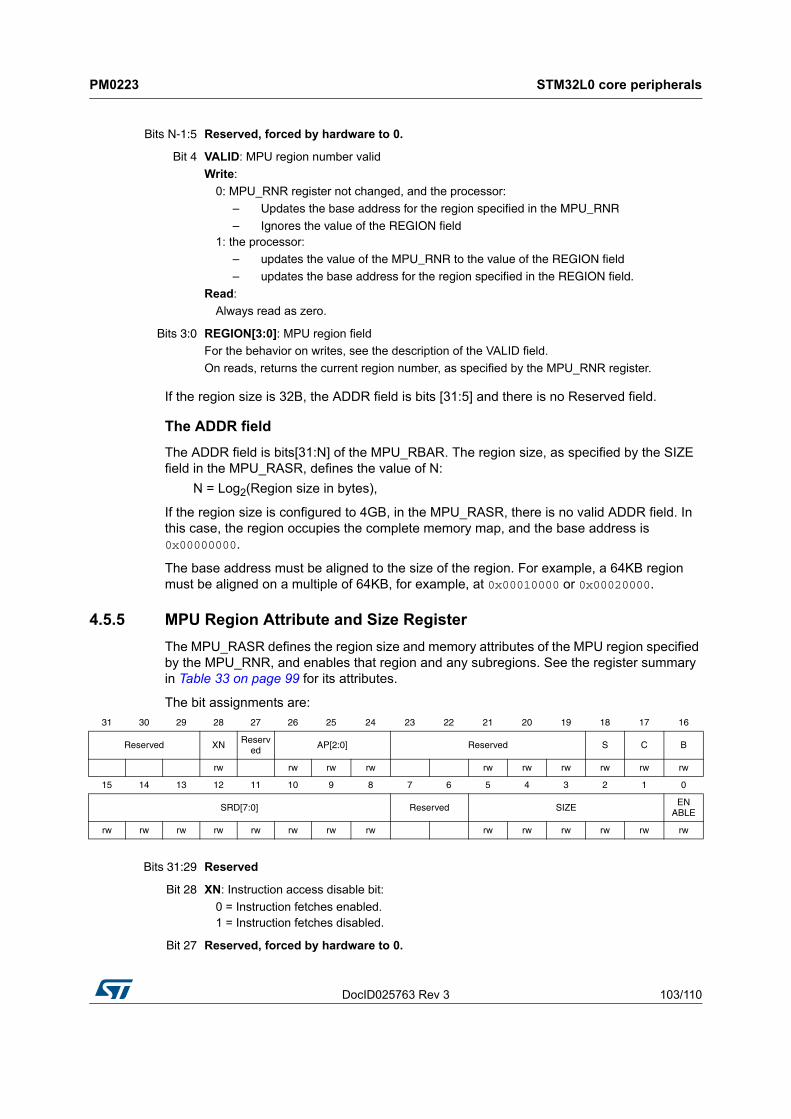
DocID025763 Rev 3 103/110
PM0223 STM32L0 core peripherals
108
If the region size is 32B, the ADDR field is bits [31:5] and there is no Reserved field.
The ADDR field
The ADDR field is bits[31:N] of the MPU_RBAR. The region size, as specified by the SIZE field in the MPU_RASR, defines the value of N:
N = Log2(Region size in bytes),
If the region size is configured to 4GB, in the MPU_RASR, there is no valid ADDR field. In this case, the region occupies the complete memory map, and the base address is 0x00000000.
The base address must be aligned to the size of the region. For example, a 64KB region must be aligned on a multiple of 64KB, for example, at 0x00010000 or 0x00020000.
4.5.5 MPU Region Attribute and Size Register
The MPU_RASR defines the region size and memory attributes of the MPU region specified by the MPU_RNR, and enables that region and any subregions. See the register summary in Table 33 on page 99 for its attributes.
The bit assignments are:
Bits N-1:5 Reserved, forced by hardware to 0.
Bit 4 VALID: MPU region number valid
Write:
0: MPU_RNR register not changed, and the processor:
– Updates the base address for the region specified in the MPU_RNR
– Ignores the value of the REGION field1: the processor:
– updates the value of the MPU_RNR to the value of the REGION field
– updates the base address for the region specified in the REGION field.
Read:
Always read as zero.
Bits 3:0 REGION[3:0]: MPU region field
For the behavior on writes, see the description of the VALID field.
On reads, returns the current region number, as specified by the MPU_RNR register.
31 30 29 28 27 26 25 24 23 22 21 20 19 18 17 16
Reserved XN Reserved AP[2:0] Reserved S C B
rw rw rw rw rw rw rw rw rw rw
15 14 13 12 11 10 9 8 7 6 5 4 3 2 1 0
SRD[7:0] Reserved SIZE EN ABLE
rw rw rw rw rw rw rw rw rw rw rw rw rw rw
Bits 31:29 Reserved
Bit 28 XN: Instruction access disable bit:
0 = Instruction fetches enabled.1 = Instruction fetches disabled.
Bit 27 Reserved, forced by hardware to 0.
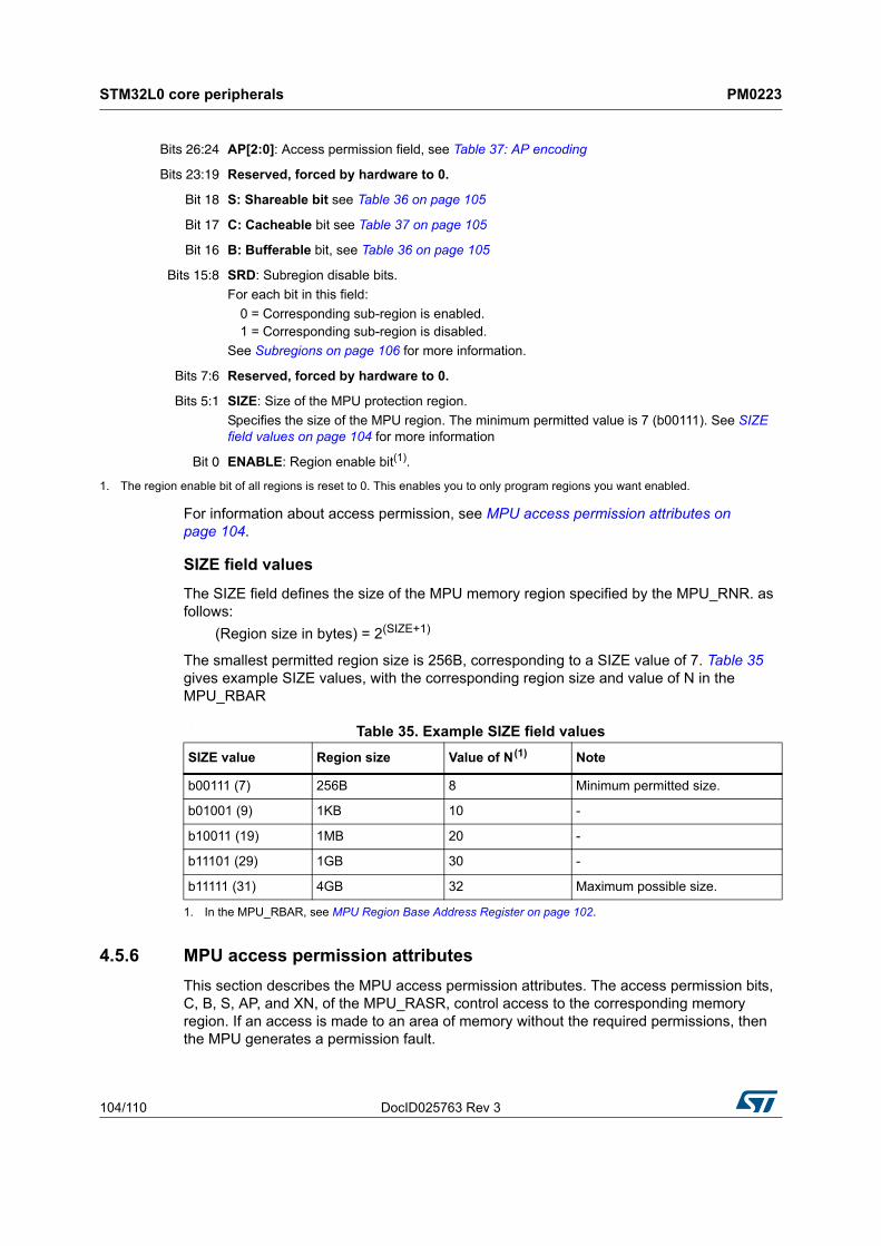
STM32L0 core peripherals PM0223
104/110 DocID025763 Rev 3
For information about access permission, see MPU access permission attributes on page 104.
SIZE field values
The SIZE field defines the size of the MPU memory region specified by the MPU_RNR. as follows:
(Region size in bytes) = 2(SIZE+1)
The smallest permitted region size is 256B, corresponding to a SIZE value of 7. Table 35 gives example SIZE values, with the corresponding region size and value of N in the MPU_RBAR
.
4.5.6 MPU access permission attributes
This section describes the MPU access permission attributes. The access permission bits, C, B, S, AP, and XN, of the MPU_RASR, control access to the corresponding memory region. If an access is made to an area of memory without the required permissions, then the MPU generates a permission fault.
Bits 26:24 AP[2:0]: Access permission field, see Table 37: AP encoding
Bits 23:19 Reserved, forced by hardware to 0.
Bit 18 S: Shareable bit see Table 36 on page 105
Bit 17 C: Cacheable bit see Table 37 on page 105
Bit 16 B: Bufferable bit, see Table 36 on page 105
Bits 15:8 SRD: Subregion disable bits.
For each bit in this field:
0 = Corresponding sub-region is enabled.1 = Corresponding sub-region is disabled.
See Subregions on page 106 for more information.
Bits 7:6 Reserved, forced by hardware to 0.
Bits 5:1 SIZE: Size of the MPU protection region.
Specifies the size of the MPU region. The minimum permitted value is 7 (b00111). See SIZE field values on page 104 for more information
Bit 0 ENABLE: Region enable bit(1).
1. The region enable bit of all regions is reset to 0. This enables you to only program regions you want enabled.
Table 35. Example SIZE field values
SIZE value Region size Value of N (1)
1. In the MPU_RBAR, see MPU Region Base Address Register on page 102.
Note
b00111 (7) 256B 8 Minimum permitted size.
b01001 (9) 1KB 10 -
b10011 (19) 1MB 20 -
b11101 (29) 1GB 30 -
b11111 (31) 4GB 32 Maximum possible size.
DocID025763 Rev 3 105/110
PM0223 STM32L0 core peripherals
108
Table 36 shows the encodings for the C, B, and S access permission bits
.
Table 37 shows the AP encodings that define the access permissions for privileged and unprivileged software
.
4.5.7 MPU mismatch
When an access violates the MPU permissions, the processor generates a HardFault.
4.5.8 Updating an MPU region
To update the attributes for an MPU region, update the MPU_RNR, MPU_RBAR and MPU_RASR registers.
Updating an MPU region
Simple code to configure one region:
; R1 = region number ; R2 = size/enable ; R3 = attributes ; R4 = address LDR R0,=MPU_RNR ; 0xE000ED98, MPU region number register
Table 36. C, B, and S encoding
C B S Memory type Shareability Other attributes
0 0 - (1)
1. The MPU ignores the value of this bit.
Strongly-ordered Shareable -
1 -(1) Device Shareable -
1
0 0
NormalNot shareable
Outer and inner write-through. No write allocate.1 Shareable
1 0
NormalNot shareable
Outer and inner write-back. No write allocate.1 Shareable
Table 37. AP encoding
AP[2:0]Privileged
permissions
Unprivileged
permissionsDescription
000 No access No access All accesses generate a permission fault.
001 RW No access Access from privileged software only.
010 RW ROWrites by unprivileged software generate a permission fault.
011 RW RW Full access.
100 Unpredictable Unpredictable Reserved.
101 RO No access Reads by privileged software only.
110 RO RO Read only, by privileged or unprivileged software.
111 RO RO Read only, by privileged or unprivileged software.
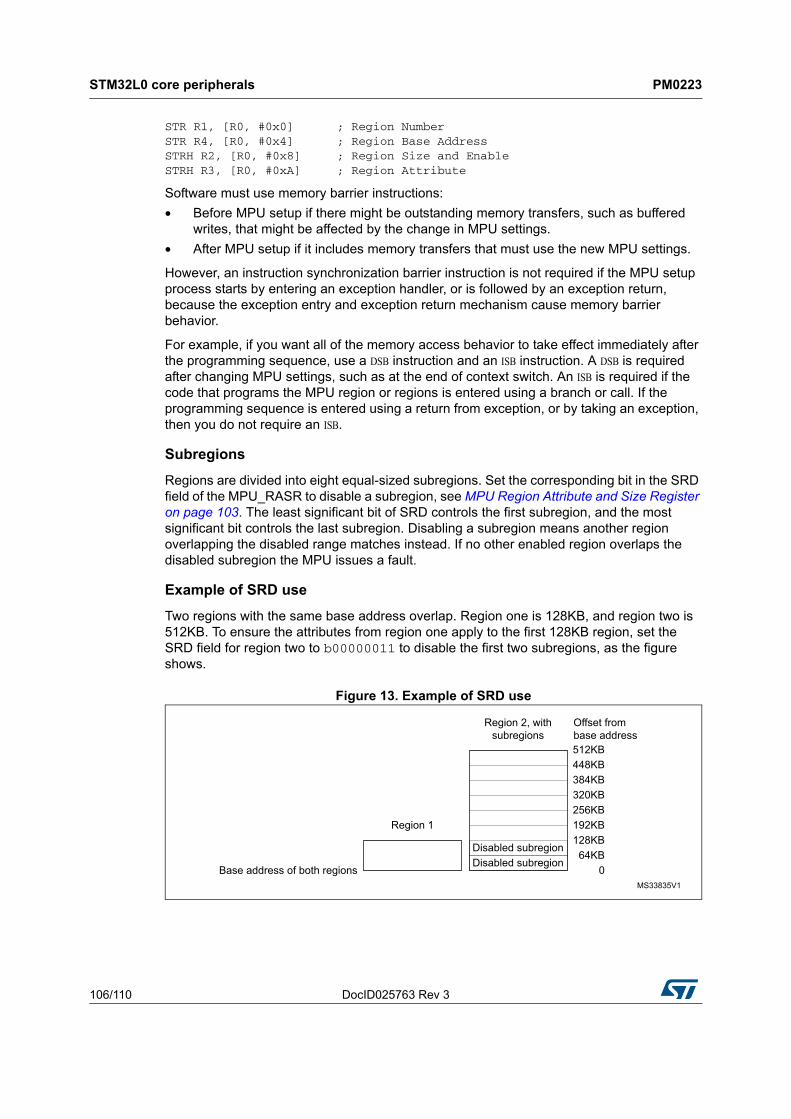
STM32L0 core peripherals PM0223
106/110 DocID025763 Rev 3
STR R1, [R0, #0x0] ; Region Number STR R4, [R0, #0x4] ; Region Base Address STRH R2, [R0, #0x8] ; Region Size and Enable STRH R3, [R0, #0xA] ; Region Attribute
Software must use memory barrier instructions:
• Before MPU setup if there might be outstanding memory transfers, such as buffered writes, that might be affected by the change in MPU settings.
• After MPU setup if it includes memory transfers that must use the new MPU settings.
However, an instruction synchronization barrier instruction is not required if the MPU setup process starts by entering an exception handler, or is followed by an exception return, because the exception entry and exception return mechanism cause memory barrier behavior.
For example, if you want all of the memory access behavior to take effect immediately after the programming sequence, use a DSB instruction and an ISB instruction. A DSB is required after changing MPU settings, such as at the end of context switch. An ISB is required if the code that programs the MPU region or regions is entered using a branch or call. If the programming sequence is entered using a return from exception, or by taking an exception, then you do not require an ISB.
Subregions
Regions are divided into eight equal-sized subregions. Set the corresponding bit in the SRD field of the MPU_RASR to disable a subregion, see MPU Region Attribute and Size Register on page 103. The least significant bit of SRD controls the first subregion, and the most significant bit controls the last subregion. Disabling a subregion means another region overlapping the disabled range matches instead. If no other enabled region overlaps the disabled subregion the MPU issues a fault.
Example of SRD use
Two regions with the same base address overlap. Region one is 128KB, and region two is 512KB. To ensure the attributes from region one apply to the first 128KB region, set the SRD field for region two to b00000011 to disable the first two subregions, as the figure shows.
Figure 13. Example of SRD use
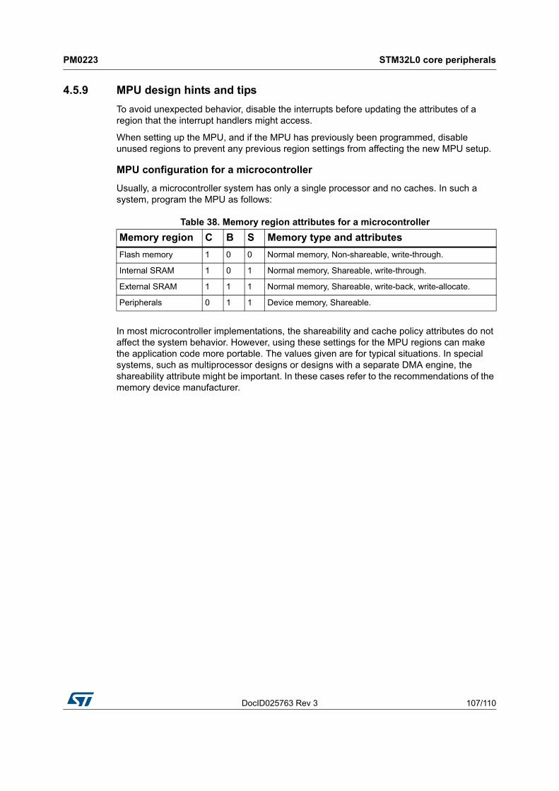
DocID025763 Rev 3 107/110
PM0223 STM32L0 core peripherals
108
4.5.9 MPU design hints and tips
To avoid unexpected behavior, disable the interrupts before updating the attributes of a region that the interrupt handlers might access.
When setting up the MPU, and if the MPU has previously been programmed, disable unused regions to prevent any previous region settings from affecting the new MPU setup.
MPU configuration for a microcontroller
Usually, a microcontroller system has only a single processor and no caches. In such a system, program the MPU as follows:
In most microcontroller implementations, the shareability and cache policy attributes do not affect the system behavior. However, using these settings for the MPU regions can make the application code more portable. The values given are for typical situations. In special systems, such as multiprocessor designs or designs with a separate DMA engine, the shareability attribute might be important. In these cases refer to the recommendations of the memory device manufacturer.
Table 38. Memory region attributes for a microcontroller
Memory region C B S Memory type and attributes
Flash memory 1 0 0 Normal memory, Non-shareable, write-through.
Internal SRAM 1 0 1 Normal memory, Shareable, write-through.
External SRAM 1 1 1 Normal memory, Shareable, write-back, write-allocate.
Peripherals 0 1 1 Device memory, Shareable.
STM32L0 core peripherals PM0223
108/110 DocID025763 Rev 3
4.6 I/O Port
STM32L0 Cortex-M0+ implements a dedicated I/O port for high-speed, low-latency access to peripherals. The I/O port is memory mapped and supports all the load and store instructions given in Memory access instructions on page 45. The I/O port does not support code execution.
The STM32L0 general-purpose I/Os are accessed through the I/O port.
The I/O port can be protected by the MPU.
DocID025763 Rev 3 109/110
PM0223 Revision history
109
5 Revision history
Table 39. Document revision history
Date Revision Changes
15-Apr-2014 1 Initial release.
16-Jun-2017 2 Updated Section 2.3.4: Vector table
19-Jan-2018 3 Updated Section 3.5.1: ADC, ADD, RSB, SBC, and SUB
PM0223
110/110 DocID025763 Rev 3
IMPORTANT NOTICE – PLEASE READ CAREFULLY
STMicroelectronics NV and its subsidiaries (“ST”) reserve the right to make changes, corrections, enhancements, modifications, and improvements to ST products and/or to this document at any time without notice. Purchasers should obtain the latest relevant information on ST products before placing orders. ST products are sold pursuant to ST’s terms and conditions of sale in place at the time of order acknowledgement.
Purchasers are solely responsible for the choice, selection, and use of ST products and ST assumes no liability for application assistance or the design of Purchasers’ products.
No license, express or implied, to any intellectual property right is granted by ST herein.
Resale of ST products with provisions different from the information set forth herein shall void any warranty granted by ST for such product.
ST and the ST logo are trademarks of ST. All other product or service names are the property of their respective owners.
Information in this document supersedes and replaces information previously supplied in any prior versions of this document.
© 2018 STMicroelectronics – All rights reserved