pn junction diode - technology innovation and incubation...
TRANSCRIPT
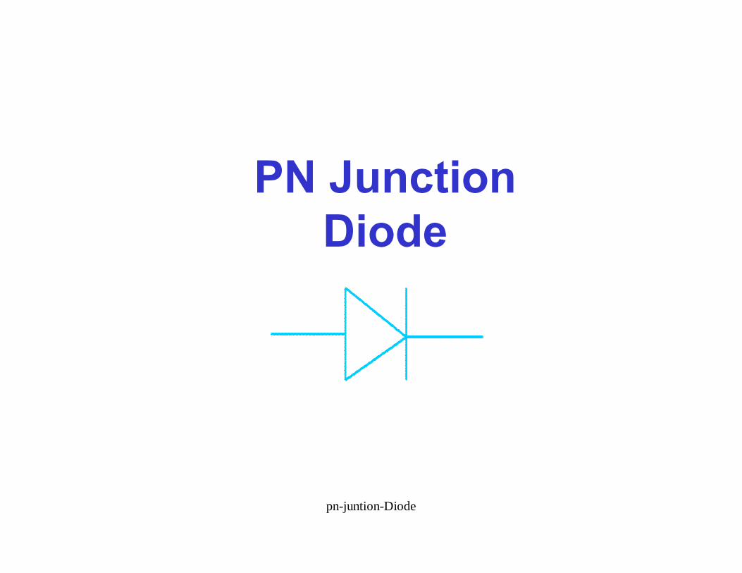
PN Junction Diode
pn-juntion-Diode
A p-n junction is the metallurgical boundary between the n and p-regions of a semiconductor crystal.
P-n junctions consist of two semiconductor regions of oppositetype. Such junctions show a pronounced rectifying behavior.They are also called p-n diodes in analogy with vacuum diodes.
The p-n junction is a versatile element, which can be used as arectifier, as an isolation structure and as a voltage-dependentcapacitor. In addition, they can be used as solar cells,photodiodes, light emitting diodes and even laser diodes. Theyare also an essential part of Metal-Oxide-Silicon Field-Effects-Transistors (MOSFETs) and Bipolar Junction Transistors (BJTs).
Basics of p-n junction?

A p-n junction consists of two semiconductor regions with oppositedoping type as shown in Figure. The region on the left is p-type withan acceptor density Na, while the region on the right is n-type with adonor density Nd. The dopants are assumed to be shallow, so thatthe electron (hole) density in the n-type (p-type) region isapproximately equal to the donor (acceptor) density.
Cross-section of a p-n junctionpn-juntion-Diode

We will assume, unless stated otherwise, that the dopedregions are uniformly doped and that the transition betweenthe two regions is abrupt. We will refer to this structure asan abrupt p-n junction.
Frequently we will deal with p-n junctions in which one side isdistinctly higher-doped than the other. We will find that insuch a case only the low-doped region needs to beconsidered, since it primarily determines the devicecharacteristics. We will refer to such a structure as a one-sided abrupt p-n junction.
The junction is biased with a voltage Va as shown in Figure.We will call the junction forward-biased if a positive voltageis applied to the p-doped region and reversed-biased if anegative voltage is applied to the p-doped region. Thecontact to the p-type region is also called the anode, whilethe contact to the n-type region is called the cathode, inreference to the anions or positive carriers and cations ornegative carriers in each of these regions.

Flatband diagram The principle of operation will be explained using a gedanken experiment, anexperiment, which is in principle possible but not necessarily executable inpractice. We imagine that one can bring both semiconductor regions together,aligning both the conduction and valence band energies of each region. Thisyields the so-called flatband diagram shown in Figure.
Energy band diagram of a p-n junction (a) before and (b) after merging the n-type and p-type regions

Note that this does not automatically align the Fermienergies, EF,n and EF,p. Also, note that this flatband diagramis not an equilibrium diagram since both electrons andholes can lower their energy by crossing the junction.
A motion of electrons and holes is therefore expectedbefore thermal equilibrium is obtained. The diagram shownin Figure (b) is called a flatband diagram. This name refersto the horizontal band edges. It also implies that there is nofield and no net charge in the semiconductor.
pn-juntion-Diode

At Thermal EquilibriumA short time after the junction is
established and thermal equilibrium isachieved, charge carriers in the vicinity ofthe junction will neutralize each other(electrons combining with holes), leavingthe unneutralized negatively ionizedacceptors, Na
- , in the p-region andunneutralized positively ionized donors,Nd
+ , in the n-region. This region ofionized donors and acceptors creates aspace charge and its region is called thedepletion region.
The edge of the depletion region given by -xp on the p-side and +xn on the n-side.the ionized donors and acceptors are located in substitutional lattice sites andCannot move in the electric field. The concentration of these donors andacceptors are selected to give the p-n junction desired device properties
pn-juntion-Diode

i.e. the Fermi level in the p- and n- typesemiconductors must be equal. Thisrequirement for constant Fermi levelpushesthe n-type semiconductor Fermi leveldown to be constant with the p-typesemiconductor Fermi level, as shown inthe diagram. The amount the bands arebent is the difference In work function.
The depletion width xd, where xd = xp + xn maybe calculated from
Drift
Diffusion
Drift
Diffusion
biad
d VNNq
x
+=
−+
112ε
0=dx
dE f
Energy Band Diagram at Thermal EquilibriumAt thermal equilibrium
Energy band diagram of a p-n junction in thermal equilibrium
While in thermal equilibrium no external voltage is appliedbetween the n-type and p-type material, there is an internalpotential, φ, which is caused by the workfunction differencebetween the n-type and p-type
pn-juntion-Diode

Impurity distribution illustrating the space charge region
Electric field variation
with distance, x
Potential variation
with distance, x
The build-in potential may
be expressed as:
2lni
dabi n
NNq
kTV+−
=
Where,
mVVq
kTT 26==
K – Boltzman constant
VT = Thermal voltage
At T=300K
Junction Potential
pn-juntion-Diode

The built-in potential in a semiconductor equals the potential across thedepletion region in thermal equilibrium. Since thermal equilibrium impliesthat the Fermi energy is constant throughout the p-n diode, the built-inpotential equals the difference between the Fermi energies, EFn and EFp,divided by the electronic charge.
It also equals the sum of the bulk potentials of each region, φn and φp,since the bulk potential quantifies the distance between the Fermi energyand the intrinsic energy. This yields the following expression for the built-in potential.
The built-in potential
pn-juntion-Diode

No Applied VoltageA semiconductor diode is created by joining the n-type semiconductor to a p-type semiconductor.
In the absence of a
bias voltage across
the diode, the net
flow of charge is one
direction is zero. Bias is
the term used when an
external DC voltage
is applied
Semiconductor Diode
pn-juntion-Diode
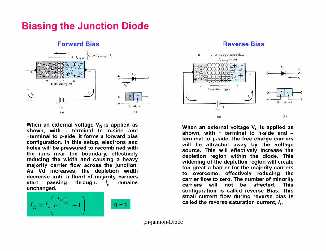
When an external voltage VD is applied asshown, with - terminal to n-side and+terminal to p-side, it forms a forward biasconfiguration. In this setup, electrons andholes will be pressured to recombined withthe ions near the boundary, effectivelyreducing the width and causing a heavymajority carrier flow across the junction.As Vd increases, the depletion widthdecrease until a flood of majority carriersstart passing through. Is remainsunchanged.
Forward Bias
n ~ 1
When an external voltage VD is applied asshown, with + terminal to n-side and –terminal to p-side, the free charge carrierswill be attracted away by the voltagesource. This will effectively increase thedepletion region within the diode. Thiswidening of the depletion region will createtoo great a barrier for the majority carriersto overcome, effectively reducing thecarrier flow to zero. The number of minoritycarriers will not be affected. Thisconfiguration is called reverse Bias. Thissmall current flow during reverse bias iscalled the reverse saturation current, Is.
Reverse Bias
−= 1T
DnV
V
sD eII
Biasing the Junction Diode
pn-juntion-Diode

We now consider a p-n diode with an applied bias voltage, Va. A forward biascorresponds to applying a positive voltage to the anode (the p-type region)relative to the cathode (the n-type region). A reverse bias corresponds to anegative voltage applied to the cathode. Both bias modes are illustrated withFigure. The applied voltage is proportional to the difference between theFermi energy in the n-type and p-type quasi-neutral regions.
As a negative voltage is applied,the potential across thesemiconductor increases and sodoes the depletion layer width. Asa positive voltage is applied, thepotential across thesemiconductor decreases andwith it the depletion layer width.The total potential across thesemiconductor equals the built-inpotential minus the appliedvoltage, or: Energy band diagram of a p-n junction under reverse and forward
bias
pn-juntion-Diode

The electrostatic analysis of a p-n diode is of interest since it providesknowledge about the charge density and the electric field in the depletionregion. It is also required to obtain the capacitance-voltage characteristics ofthe diode. The analysis is very similar to that of a metal-semiconductorjunction. A key difference is that a p-n diode contains two depletion regionsof opposite type.
Electrostatic analysis of a p-n diode
pn-juntion-Diode

What Are Diodes Made Out Of?
• Silicon (Si) and Germanium (Ge) are the two mostcommon single elements that are used to make Diodes.A compound that is commonly used is GalliumArsenide (GaAs), especially in the case of LEDsbecause of it’s large bandgap.
• Silicon and Germanium are both group 4 elements,meaning they have 4 valence electrons. Theirstructure allows them to grow in a shape called thediamond lattice.
• Gallium is a group 3 element while Arsenide is a group5 element. When put together as a compound, GaAscreates a zincblend lattice structure.
• In both the diamond lattice and zincblend lattice, eachatom shares its valence electrons with its four closestneighbors. This sharing of electrons is what ultimatelyallows diodes to be build. When dopants from groups3 or 5 (in most cases) are added to Si, Ge or GaAs itchanges the properties of the material so we are ableto make the P- and N-type materials that become thediode.
Si+4
Si+4
Si+4
Si +4
Si+4
Si+4
Si+4
Si+4
Si+4
The diagram above shows the2D structure of the Si crystal.The light green linesrepresent the electronicbonds made when the valenceelectrons are shared. Each Siatom shares one electron witheach of its four closestneighbors so that its valenceband will have a full 8electrons.
pn-juntion-Diode

N-Type Material:When extra valence electrons are introduced intoa material such as silicon an n-type material isproduced. The extra valence electrons areintroduced by putting impurities or dopants intothe silicon. The dopants used to create an n-typematerial are Group V elements. The mostcommonly used dopants from Group V arearsenic, antimony and phosphorus.
The 2D diagram to the left shows the extraelectron that will be present when a Group Vdopant is introduced to a material such as silicon.This extra electron is very mobile.
+4+4
+5
+4
+4+4+4
+4+4
pn-juntion-Diode

P-Type Material:P-type material is produced when the dopant thatis introduced is from Group III. Group IIIelements have only 3 valence electrons andtherefore there is an electron missing. Thiscreates a hole (h+), or a positive charge that canmove around in the material. Commonly usedGroup III dopants are aluminum, boron, andgallium.
The 2D diagram to the left shows the hole thatwill be present when a Group III dopant isintroduced to a material such as silicon. Thishole is quite mobile in the same way the extraelectron is mobile in a n-type material.
+4+4
+3
+4
+4+4+4
+4+4
pn-juntion-Diode

The PN JunctionSteady State1
P n
- - - - - -
- - - - - -
- - - - - -
- - - - - -
- - - - - -
+ + + + + +
+ + + + + +
+ + + + + +
+ + + + + +
+ + + + + +
Na NdMetallurgical
Junction
Space Charge Regionionized
acceptorsionized donors
E-Field
++ _ _
h+ drift h+ diffusion e- diffusion e- drift= =pn-juntion-Diode

The PN JunctionSteady State
P n
- - - - -
- - - - -
- - - - -
- - - - -
+ + + + +
+ + + + +
+ + + + +
+ + + + +
Na NdMetallurgical
Junction
Space Charge Regionionized
acceptorsionized donors
E-Field++ _ _
h+ drift h+ diffusion e- diffusion e- drift= == =
When no external source is connected to the pn junction, diffusion and drift balance each other out for both the holes
and electrons
Space Charge Region: Also called the depletion region. This region includes the net positively and negatively charged regions. The space charge region does not have any free carriers. The width of the space charge region is denoted by W in pn junction formula’s.
Metallurgical Junction: The interface where the p- and n-type materials meet.
Na & Nd: Represent the amount of negative and positive doping in number of carriers per centimeter cubed. Usually in the range of 1015 to 1020.
pn-juntion-Diode

The Biased PN Junction
P n+_
Applied Electric Field
Metal Contact
“Ohmic Contact”
(Rs~0)
+ _
Vapplied
I
The pn junction is considered biased when an external voltage is applied. There are two types of biasing: Forward bias and Reverse bias.
These are described on then next slide.pn-juntion-Diode

The Biased PN Junction
Forward Bias: In forward bias the depletion region shrinks slightly in width. Withthis shrinking the energy required for charge carriers to cross thedepletion region decreases exponentially. Therefore, as theapplied voltage increases, current starts to flow across thejunction. The barrier potential of the diode is the voltage at whichappreciable current starts to flow through the diode. The barrierpotential varies for different materials.
Reverse Bias: Under reverse bias the depletion region widens. This causes theelectric field produced by the ions to cancel out the appliedreverse bias voltage. A small leakage current, Is (saturationcurrent) flows under reverse bias conditions. This saturationcurrent is made up of electron-hole pairs being produced in thedepletion region. Saturation current is sometimes referred to asscale current because of it’s relationship to junction temperature.
Vapplied > 0
Vapplied < 0
pn-juntion-Diode

Properties of DiodesFigure 1.10 – The Diode Transconductance Curve2
• VD = Bias Voltage
• ID = Current through Diode. ID is Negative for Reverse Bias and Positive for Forward Bias
• IS = Saturation Current
• VBR = Breakdown Voltage
• Vφ = Barrier Potential Voltage
VD
ID (mA)
(nA)
VBR
~Vφ
IS
pn-juntion-Diode

Properties of DiodesThe Shockley Equation
• The transconductance curve on the previous slide is characterized by the following equation:
ID = IS(eVD/ηVT – 1)• As described in the last slide, ID is the current through the diode, IS is the
saturation current and VD is the applied biasing voltage.
• VT is the thermal equivalent voltage and is approximately 26 mV at room temperature. The equation to find VT at various temperatures is:
VT = kTq
k = 1.38 x 10⁻²³ J/K T = temperature in Kelvin q = 1.6 x 10⁻¹⁹ C
• η is the emission coefficient for the diode. It is determined by the way the diode is constructed. It somewhat varies with diode current. For a silicon diode η is around 2 for low currents and goes down to about 1 at higher currents
pn-juntion-Diode

Diode Circuit ModelsThe Ideal Diode
ModelThe diode is designed to allow current to flow in only one direction. The perfect diode would be a perfect conductor in one direction (forward bias) and a perfect insulator in the other direction (reverse bias). In many situations, using the ideal diode approximation is acceptable.
Example: Assume the diode in the circuit below is ideal. Determine the value of ID if a) VA = 5 volts (forward bias) and b) VA = -5 volts (reverse bias)
+
_VA
ID
RS = 50 Ω a) With VA > 0 the diode is in forward bias and is acting like a perfect conductor so:
ID = VA/RS = 5 V / 50 Ω = 100 mA
b) With VA < 0 the diode is in reverse bias and is acting like a perfect insulator, therefore no current can flow and ID = 0.
pn-juntion-Diode

Diode Circuit ModelsThe Ideal Diode with
Barrier PotentialThis model is more accurate than the simple ideal diode model because it includes the approximate barrier potential voltage. Remember the barrier potential voltage is the voltage at which appreciable current starts to flow.
Example: To be more accurate than just using the ideal diode model include the barrier potential. Assume Vφ = 0.3 volts (typical for a germanium diode) Determine the value of ID if VA = 5 volts (forward bias).
+
_VA
ID
RS = 50 Ω With VA > 0 the diode is in forward bias and is acting like a perfect conductor so write a KVL equation to find ID:0 = VA – IDRS - Vφ
ID = VA - Vφ = 4.7 V = 94 mA RS 50 Ω
Vφ
+
Vφ+
pn-juntion-Diode
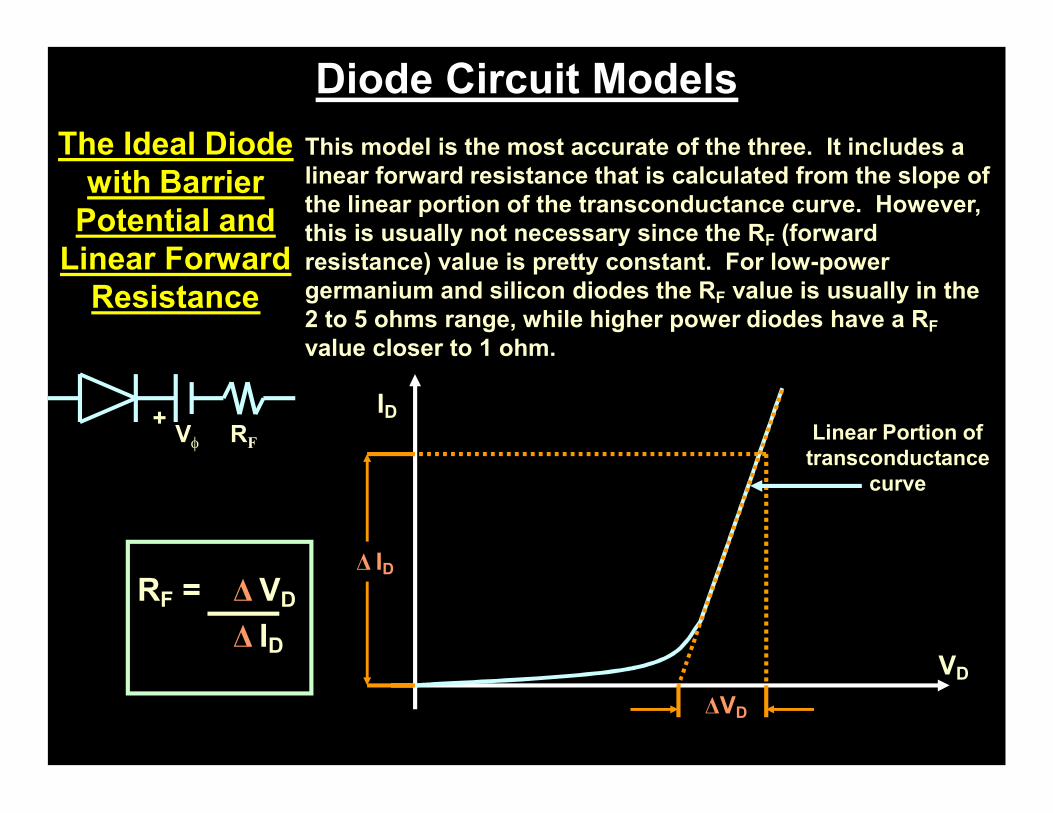
Diode Circuit ModelsThe Ideal Diode
with Barrier Potential and
Linear Forward Resistance
This model is the most accurate of the three. It includes a linear forward resistance that is calculated from the slope of the linear portion of the transconductance curve. However, this is usually not necessary since the RF (forward resistance) value is pretty constant. For low-power germanium and silicon diodes the RF value is usually in the 2 to 5 ohms range, while higher power diodes have a RFvalue closer to 1 ohm.
Linear Portion of transconductance
curve
VD
ID
ΔVD
Δ IDRF = Δ VD
Δ ID
+ Vφ RF
pn-juntion-Diode

Diode Circuit ModelsThe Ideal Diode
with Barrier Potential and
Linear Forward Resistance
Example: Assume the diode is a low-power diode with a forward resistance value of 5 ohms. The barrier potential voltage is still: Vφ = 0.3 volts (typical for a germanium diode) Determine the value of ID if VA = 5 volts.
+
_VA
ID
RS = 50 Ω
Vφ+
RF
Once again, write a KVL equation for the circuit:
0 = VA – IDRS - Vφ - IDRF
ID = VA - Vφ = 5 – 0.3 = 85.5 mARS + RF 50 + 5
pn-juntion-Diode

Diode Circuit ModelsValues of ID for the Three Different Diode Circuit Models
Ideal Diode Model
Ideal Diode Model with
Barrier Potential Voltage
Ideal Diode Model with
Barrier Potential and
Linear Forward Resistance
ID 100 mA 94 mA 85.5 mA
These are the values found in the examples on previous slideswhere the applied voltage was 5 volts, the barrier potential was0.3 volts and the linear forward resistance value was assumed tobe 5 ohms. pn-juntion-Diode
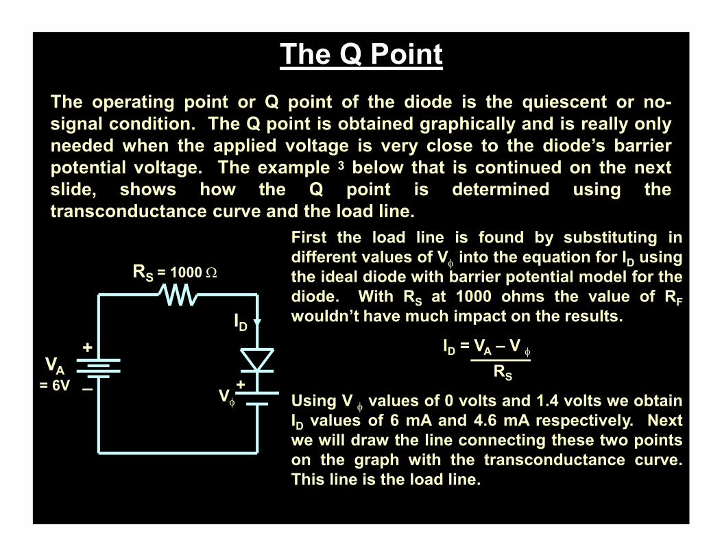
The Q PointThe operating point or Q point of the diode is the quiescent or no-signal condition. The Q point is obtained graphically and is really onlyneeded when the applied voltage is very close to the diode’s barrierpotential voltage. The example 3 below that is continued on the nextslide, shows how the Q point is determined using thetransconductance curve and the load line.
+
_VA
= 6V
ID
RS = 1000 Ω
Vφ+
First the load line is found by substituting indifferent values of Vφ into the equation for ID usingthe ideal diode with barrier potential model for thediode. With RS at 1000 ohms the value of RFwouldn’t have much impact on the results.
ID = VA – V φ
RS
Using V φ values of 0 volts and 1.4 volts we obtainID values of 6 mA and 4.6 mA respectively. Nextwe will draw the line connecting these two pointson the graph with the transconductance curve.This line is the load line.
pn-juntion-Diode

The Q PointID (mA)
VD (Volts)
2
4
6
8
10
12
0.2 0.4 0.6 0.8 1.0 1.2 1.4
The transconductance
curve below is for a Silicon diode. The
Q point in this example is located at 0.7 V and 5.3 mA.
4.6
0.7
5.3
Q Point: The intersection of the load line and the transconductance curve.
pn-juntion-Diode

Dynamic ResistanceThe dynamic resistance of the diode is mathematically determinedas the inverse of the slope of the transconductance curve.Therefore, the equation for dynamic resistance is:
rF = ηVT
IDThe dynamic resistance is used in determining the voltage dropacross the diode in the situation where a voltage source issupplying a sinusoidal signal with a dc offset.
The ac component of the diode voltage is found using thefollowing equation:
vF = vac rF
rF + RSThe voltage drop through the diode is a combination of the ac anddc components and is equal to:
VD = Vφ + vFpn-juntion-Diode

Dynamic Resistance
Example: Use the same circuit used for the Q point example but change the voltage source so it is an ac source with a dc offset. The source voltage is now, vin = 6 + sin(wt) Volts. It is a silicon diode so the barrier potential voltage is still 0.7 volts.
+vin
ID
RS = 1000 Ω
Vφ+
The DC component of the circuit is the same as the previous example and therefore ID = 6V – 0.7 V = 5.2 mA
1000 ΩrF = ηVT = 1 * 26 mV = 4.9 Ω
ID 5.3 mA
η = 1 is a good approximation if the dc current is greater than 1 mA as it is in this
example.vF = vac rF = sin(wt) V 4.9 Ω = 4.88 sin(wt) mV
rF + RS 4.9 Ω + 1000 Ω
Therefore, VD = 700 + 4.9 sin (wt) mV (the voltage drop across the diode)
pn-juntion-Diode

Types of Diodes and Their Uses
PN Junction Diodes:
Are used to allow current to flow in one direction while blocking current flow in the opposite direction. The pn junction diode is the typical diode that has been used in the previous circuits.
A K
Schematic Symbol for a PN Junction Diode
P n
Representative Structure for a PN Junction Diode
Zener Diodes: Are specifically designed to operate under reverse breakdown conditions. These diodes have a very accurate and specific reverse breakdown voltage.
A K
Schematic Symbol for a Zener Diode pn-juntion-Diode

Types of Diodes and Their Uses
Schottky Diodes:
These diodes are designed to have a very fast switching time which makes them a great diode for digital circuit applications. They are very common in computers because of their ability to be switched on and off so quickly. A K
Schematic Symbol for a Schottky Diode
Shockley Diodes:
The Shockley diode is a four-layer diode while other diodes are normally made with only two layers. These types of diodes are generally used to control the average power delivered to a load.
A K
Schematic Symbol for a four-layer Shockley Diode
pn-juntion-Diode

Types of Diodes and Their Uses
Light-Emitting Diodes:
Light-emitting diodes are designed with a very large bandgap so movement of carriers across their depletion region emits photons of light energy. Lower bandgap LEDs (Light-Emitting Diodes) emit infrared radiation, while LEDs with higher bandgap energy emit visible light. Many stop lights are now starting to use LEDs because they are extremely bright and last longer than regular bulbs for a relatively low cost.
A K
Schematic Symbol for a Light-Emitting Diode
The arrows in the LED representation indicate
emitted light.
pn-juntion-Diode

Types of Diodes and Their Uses
Photodiodes: While LEDs emit light, Photodiodes are sensitive to received light. They are constructed so their pn junction can be exposed to the outside through a clear window or lens.
In Photoconductive mode the saturation current increases in proportion to the intensity of the received light. This type of diode is used in CD players.
In Photovoltaic mode, when the pn junction is exposed to a certain wavelength of light, the diode generates voltage and can be used as an energy source. This type of diode is used in the production of solar power.
A K
A K
Schematic Symbols for Photodiodes
λ
pn-juntion-Diode

ReferencesDailey, Denton. Electronic Devices and Circuits, Discrete and Integrated. Prentice Hall, New
Jersey: 2001. (pp 2-37, 752-753)2 Figure 1.10. The diode transconductance curve, pg. 7Figure 1.15. Determination of the average forward resistance of a diode, pg 113 Example from pages 13-14
Liou, J.J. and Yuan, J.S. Semiconductor Device Physics and Simulation. Plenum Press, New York: 1998.
Neamen, Donald. Semiconductor Physics & Devices. Basic Principles. McGraw-Hill, Boston: 1997. (pp 1-15, 211-234)1 Figure 6.2. The space charge region, the electric field, and the forces acting on
the charged carriers, pg 213.
pn-juntion-Diode