politecnico di milano · politecnico di milano ... siti sono stati tradotti nella realizzazione del...
TRANSCRIPT

POLITECNICO DI MILANO Scuola di Ingegneria dell’informazione
POLO TERRITORIALE DI COMO
Master of Science in Computer Engineering
Design of an optimized audio framework
for portable digital MEMS microphones
evaluation
Supervisor: Prof. Augusto Sarti
Assistant Supervisor: Marco Brugora
Master Graduation Thesis by: Riccardo Canta
Student ID Number: 754573
Academic year 2011/12
POLITECNICO DI MILANO Scuola di Ingegneria dell’informazione
POLO TERRITORIALE DI COMO
Corso di Laurea Specialistica in Ingegneria Informatica
Design di un framework audio ottimizzato
per la valutazione di microfoni digitali
MEMS
Relatore: Prof. Augusto Sarti
Correlatore: Marco Brugora
Tesi di laurea di: Riccardo Canta
Matricola:754573
Anno Accademico 2011/12
Sommario
I sistemi audio, nel corso della loro evoluzione, stanno modificando i modelli per
il trasferimento e l’acquisizione di dati. Questo implica una necessità di metodo-
logie di test e strumenti capaci di misurarne le prestazioni. Le limitazioni degli
strumenti odierni sono principalmente legate a fattori di costo e dimensioni. I mi-
crocontrollori, con la loro adattabilità e flessibilità, possono essere adottati per
questo utilizzo con vantaggi in termini di portabilità. Un dispositivo di acquisizio-
ne/emissione che comunica tramite USB con un PC permette di ottenere un siste-
ma stabile e senza le limitazioni legate ad architetture fisse e agli svantaggi
dell’analogico. Le sue funzionalità sono la valutazione di microfoni digitali
MEMS, la comunicazione I2C via HID, l’aggiornamento DFU e la possibilità di
memorizzare le configurazioni su NVM. Questo lavoro copre l’intero flusso della
progettazione dello strumento partendo dalla definizione delle specifiche. I requi-
siti sono stati tradotti nella realizzazione del framework ed il sistema è stato testa-
to. Sviluppi futuri sono principalmente connessi all’ampliamento del lato software
del framework per migliorarne ed estenderne le funzionalità e incrementarne la
precisione di misura ottenendo una piattaforma più completa e versatile.

Abstract
Modern audio systems are moving toward novel communication paradigms and
these results in testing methodologies and tools able to demonstrate them. Limita-
tions related to nowadays equipment mainly concern with costs and dimension
factors. Microcontrollers, with their adaptability and flexibility, can be adopted
for this functioning with extreme advantages for portability. An acquisi-
tion/emission device communicating over USB with a host allows a stable and
multi-purpose system for stereo I2S digital audio stream without limits due to
fixed architecture or to analog disadvantages. PDM MEMS microphone evalua-
tion, I2C communication over HID, device firmware upgrade and re-bootable
configurations with non-volatile memory are its functionalities. This work covers
the whole design flow of the tool starting with device specification and require-
ments statement. Afterwards, the requirements are translated to the application de-
sign and the evaluation board has been implemented and tested in its quality and
robustness. As for future work, could be incremented the software-side tool effi-
ciency and precision with the purpose of further optimized and complete platform.

Acknowledgment
This work has been done as part of a project in ST Microelectronics s.r.l. I would
like to thank my co-supervisor there, Mr. Marco Brugora, and all my colleagues
for helping me through the work. I am deeply indebted to my supervisor, Profes-
sor Augusto Sarti for his supervision. And finally, I wish to thank my mother and
my father for their unending love and support.
Contents Sommario ............................................................................................................... I
Abstract ................................................................................................................. II Acknowledgment ................................................................................................. III Contents .............................................................................................................. IV List of Figures ..................................................................................................... VI List of Tables .................................................................................................... VIII
List of Acronyms ................................................................................................ IX Chapter 1 ................................................................................................................ 1 Introduction ............................................................................................................ 1
Chapter 2 ................................................................................................................ 4 State of the Art ....................................................................................................... 4 Chapter 3 ................................................................................................................ 7 Development platform ........................................................................................... 7
3.1 Microcontrollers .................................................................................... 7
3.1.1 ARM M3 ...................................................................................... 10
3.1.2 STM32 ......................................................................................... 11 3.2 Host ..................................................................................................... 14 3.3 Device Under Test ............................................................................... 14
Chapter 4 .............................................................................................................. 15 Protocols & Coding algorithms ........................................................................... 15
4.1 Protocols .............................................................................................. 15 4.1.1 I2C ................................................................................................ 16
4.1.2 I2S ................................................................................................ 18 4.1.3 USB .............................................................................................. 18
4.2 Coding algorithms ............................................................................... 23 4.2.1 PDM - Pulse Density Modulation ................................................ 24 4.2.2 PCM - Pulse Code Modulation .................................................... 24
Chapter 5 .............................................................................................................. 26 Specification & Requirements ............................................................................. 26
5.1 Portability ............................................................................................ 27 5.2 Scalability ............................................................................................ 27
5.3 Reliability & Performance .................................................................. 29 5.4 Cost...................................................................................................... 29
Chapter 6 .............................................................................................................. 31
Implementation .................................................................................................... 31 6.1 Device Design ..................................................................................... 31 6.2 Firmware Design ................................................................................. 33
6.2.1 Clock Tree .................................................................................... 34
6.2.2 Audio State Machine .................................................................... 38 6.2.3 Audio USB synchronization ........................................................ 39 6.2.4 PDM acquisition .......................................................................... 43 6.2.5 USB HID/audio IAD .................................................................... 45 6.2.6 Eeprom/RAM reboot .................................................................... 46
6.2.7 DFU .............................................................................................. 46 6.3 Software Design .................................................................................. 47

6.4 Firmware Development ....................................................................... 50
6.4.1 I2C Init ......................................................................................... 50 6.4.2 SPI3 Remap .................................................................................. 51 6.4.3 USB HID parser ........................................................................... 51 6.4.4 EXTI trigger ................................................................................. 53 6.4.5 PDM crystal-dependent artefacts ................................................. 53
6.4.6 USB supply .................................................................................. 54 6.4.7 I2S macro-cell .............................................................................. 56 6.4.8 DFU/Application subdivision ...................................................... 58
6.5 Software Development ........................................................................ 60 6.5.1 HID communication ..................................................................... 60
Chapter 7 .............................................................................................................. 63
Tool Test .............................................................................................................. 63
7.1 PDM .................................................................................................... 63 7.2 I2S stream ............................................................................................ 64 7.3 HID/FTDI ............................................................................................ 68 7.4 HID robustness .................................................................................... 70
Chapter 8 .............................................................................................................. 73 Conclusion and future work ................................................................................. 73
8.1 Future Work ........................................................................................ 74
Appendix .............................................................................................................. 75 MEMS Microphone - MP34DT01 ............................................................... 75
APWorkbench............................................................................................... 75 APWLink ...................................................................................................... 76 APWLink+ .................................................................................................... 76
STA326/8/9 .................................................................................................. 76 STA321MPL ................................................................................................ 77
STLINK – V2 ............................................................................................... 78 SWD cable .................................................................................................... 78
Bibliography ........................................................................................................ 80
List of Figures
Figure 1 – Audio Precision .......................................................................................... 5 Figure 2 – MAX98089 EVKIT map ............................................................................ 6 Figure 3 – Cortex-M3 processor ................................................................................ 10 Figure 4 – System Architecture.................................................................................. 11 Figure 5 - STM32F10xxx Family .............................................................................. 12
Figure 6 - STM32F107RC pinout .............................................................................. 13 Figure 7 – I2C Write command/ack for Master Tx - Slave Rx .................................. 16 Figure 8 – I2C Read command/ack for Master Tx - Slave Rx................................... 17
Figure 9 – I2S WS and 16-bit SDA lines ................................................................... 18 Figure 10 – HID class descriptor structure. ............................................................... 21 Figure 11 – IAD descriptor ........................................................................................ 22 Figure 12 – PDM coded sinusoid ............................................................................... 24 Figure 13 – PAM sampling ........................................................................................ 25
Figure 14 - APWLink+ schematic diagram ............................................................... 32
Figure 15 - APWLink+ .............................................................................................. 33 Figure 16 - clock tree 8MHz scheme ......................................................................... 34 Figure 17 - table 8MHz quartz ................................................................................... 35
Figure 18 - table 14.7456MHz quartz ........................................................................ 36 Figure 19 - clock tree 14.7456MHz scheme .............................................................. 37
Figure 20 - clock tree 12.288MHz scheme ................................................................ 38 Figure 21 - state machine approach scheme .............................................................. 39
Figure 22 – Under-run condition................................................................................ 40 Figure 23 – Over-run condition.................................................................................. 41
Figure 24 – PDM acquisition ..................................................................................... 43 Figure 25 – SPI1 DMA interrupt handler .................................................................. 44 Figure 26 – Eeprom vs Emulated Eeprom ................................................................. 46
Figure 27 – APW Mems Microphones Demo Kit startup.......................................... 48 Figure 28 – APW ST Smart Voice Demo Kit ............................................................ 49
Figure 29 – HID parser .............................................................................................. 52 Figure 30 – MCO selector .......................................................................................... 54
Figure 31 – LM317 PSRR ......................................................................................... 55 Figure 32 – LD1086DT25 PSRR ............................................................................... 55 Figure 33 – Audio HUB schematic diagram .............................................................. 56
Figure 34 – STM32 I2S Macro-cell ........................................................................... 57 Figure 35 – Memory location map ............................................................................. 58 Figure 36 – Flash memory offset ............................................................................... 59 Figure 37 – HID software interface ........................................................................... 61
Figure 38 – HID APWLnk+ testing Framework ....................................................... 62 Figure 39 – 16-bit SDA, WS 48kHz and SCK .......................................................... 65 Figure 40 – I2S SCK bit-clock ................................................................................... 65 Figure 41 – Over-run artefacts ................................................................................... 66 Figure 42 – Audio Precision 500Hz acquisition ........................................................ 67
Figure 43 – proposed tool 500Hz acquisition ............................................................ 67 Figure 44 – Screenshot FTDI I2C performances ....................................................... 68
Figure 45 – Screenshot HID I2C performances ......................................................... 69
Figure 46 – Screenshot HID I2C overlapped performances ...................................... 70 Figure 47 – Screenshot HID I2C overlapped performances ...................................... 71 Figure 48 – Screenshot single HID I2C transaction .................................................. 72 Figure 49 – MEMS Microphone - MP34DT01 ......................................................... 75 Figure 50 – STA321MPL .......................................................................................... 77
Figure 51 – STLINK – V2 ......................................................................................... 78 Figure 52 – SWD cable _STLINK – V2 .................................................................... 79

List of Tables
Table 1 - Audio HUB Specifications ......................................................................... 28 Table 2 – Endpoints subdivision by USB classes ...................................................... 45
List of Acronyms
MCU: Micro Controller Unit
HID: Human Interface Device
IAD: Interface Association Descriptor
USB: Universal Serial Bus
PDM: Pulse Density Modulation
PCM: Pulse Code Modulation
VCP: Virtual Com Port
MEMS: Micro Electro Mechanical System
DFU: Device Firmware Upgrade
I2S: Integrated Inter-chip Sound
SD: Serial Data
WS: Word Select
SCK: Continuous Serial Clock
MSB: Most Significant Bit
LSB: Least Significant Bit
I2C: Inter Integrated Circuit
HSE: External High Speed Clock
EEPROM: Electrically Erasable Programmable Read Only Memory
GPIO: General Purpose Input Output
SPI: Serial Peripheral Interface
ISA: Instruction Set Architecture
SCL: Serial Clock Line
SDA: Serial Data Line
SWD: Serial Wire Debugging
NVM: Non-Volatile Memory
DUT: Device Under Test
MEMS: Micro Electronic Motion Sensor
NVIC: Nested Vector Interrupt Controller
DMA: Direct Memory Access
ICode: Instruction Code
DCode: Data Code
PSRR: Power Supply Rejection Ratio
PCB: Print Circuit Board
ASIC: Application Specific Integrated Circuit
ICP: In Circuit Programming
IAP: In Application Programming

1
Chapter 1
Introduction
This chapter proposes a general description of the project objectives. The work is about
the design of an audio framework for the evaluation and demonstration of digital MEMS
microphones.
Micro Electro-Mechanical Systems (MEMS) are broadly diffused in nowadays devices
such as smart phones and tablets. They provide sensors and actuators for a wide range of
applications, such as accelerometers, gyroscopes, and pressure sensors.
A particular application that is gaining importance is the use of MEMS as pressure sen-
sors for digital microphones. The source acquisition in such microphones is directly pro-
cessed by an internal component, which performs the Analog to Digital conversion in
Pulse Density Modulation (PDM) format. Today the characterization of MEMS micro-
phones requires expensive equipment with huge physical size.
The main goal of this work is to create a complete digital stream from the AD converter
of the MEMS microphone to the host and back to the microphone. This solution enables a
2
quasi-full-digital audio chain that is perceptively lossless, with a low-level of channel
noise. The channel with minimal distortion allows building a portable and cheap method-
ology for a qualitative evaluation of digital MEMS microphones, elaborating the signal at
the host side with ad-hoc software.
The proposed framework is organized in three blocks: the host, the microcontroller and
the Device Under Test (equipped with the microphone to evaluate). The audio chain is
composed by a microcontroller as a bridge to connect the host with the DUT. The choice
of a microcontroller is due to the compactness and the reliability of this technology for
real-time applications. The protocol adopted for host-side digital connection is the USB.
This protocol has been chosen for its wide diffusion and also because it has a dedicated
class for audio streaming. The microcontroller is connected to the DUT with the I2S au-
dio protocol. This protocol is a standard for digital audio applications and enables an ex-
act data transmission from/to the USB channel. USB transmission for real-time audio ap-
plications is lossy, but the error is acceptable because it can be handled by interpolation
algorithms and therefore removable in the presented application.
The proposed audio framework provides a digital audio streaming directed from the host
to a speaker directed to the digital MEMS microphone. The signal is then acquired by the
microphone and streamed back to the host. The microphone is placed in anechoic envi-
ronment in order to reduce ambient noise. The host side elaboration allows audio pro-
cessing such as Graphic equalizer, Filter design, Frequency analyzer (FFT), Scope and
waveform monitors, Waveform generator, and Sound recorder/playback.
The use of a dual socket approach is needed for a reliable characterization of digital
MEMS microphones. Dual socket approach means that the set-up is composed by a refer-
ence microphone called Golden Sample and the microphone under test.
The unknown sensitivity of the DUT can be characterized knowing the reference sensitiv-
ity and visualizing the two microphones FFTs in anechoic environment. This is only one
of the features of the proposed solution.
The audio framework is configurable in four modes of use. The first is the PDM capture
mode for the acquisition of the signal coming from the digital microphone by the micro-
controller in PDM format, followed by the software PDM to PCM conversion. The se-
cond is the acquisition of digital audio from a device equipped with digital MEMS micro-

3
phones with the ability of dynamic configurability of the device under test for hardware
filtering. The third mode is based on the first one and it enables the output stream for the
on board microphones. The fourth is the full digital I2S solution where the output signal
is acquired without background channel noise. The only constraint, as already mentioned,
is related to USB channel that does not allow a completely lossless communication.
The document is organized in these areas. Chapter 2 exposes the State of the Art of test-
ing and evaluation technologies in literature. The research has been conducted mainly on
commercial products or prototypes related to the field of application because of the lack
of literature related to digital MEMS microphones testing methodologies. Chapter 3 ex-
plains the development platform elements chose for the proposed solution. In Chapter 4
are introduced the protocols and coding algorithms involved in this work. The chosen
protocols and coding models are a standard in IT applications and therefore a quasi-
obliged choice for compatibility with the device under testing. Chapter 5 points out Speci-
fications & Requirements. It defines implementation constraints and clearly highlights the
platform features. The proposed solution, as already mentioned, mainly focus on perspec-
tive evaluation with high advantages in terms of cost and dimension. The Chapter 6 is
completely dedicated to Implementation divided in two stages (Design and Development)
and three implementation environments (Hardware, Firmware and Software). Chapter 7
regards the Test of the proposed framework. It illustrates the features reliability and con-
firms the expected performances. Chapter 8 is related to Conclusion and Future Work.
Perspectives suggest the possibility of a gradual switch from a qualitative to a quantitative
measuring of digital MEMS microphones characteristics. The proposed solution is there-
fore a hybrid in testing/evaluation worlds and therefore a novel approach in this context.
The novel audio framework is constituted by three main physical blocks related to the ac-
tual elements involved in the platform.
4
Chapter 2
State of the Art
The research about the state of the art has been conducted with a different approach than
the traditional one. The developed audio framework is an applicative solution and there-
fore it is not attributable to university research. It uses known protocols and algorithms in
a novel way. The research has been focused on tools for digital MEMS microphone char-
acterization and demonstration. Microphones in general can be characterized in detail
with measurement related to directionality, sensitivity in anechoic environment, power
consumption and robustness to extreme conditions. These tests are performed on a per-
centage of produced samples. A digital MEMS microphone is also valuable in its practi-
cal usage and in commerce are present evaluation boards which allow host acquisition.
The study is therefore mainly subdivides the tool typologies into two families: testing
tools and evaluation boards.
Testing tools are well equipped machines with many features and, among others, the
MEMS characterization. This is performed with PDM acquisition and detailed analysis.
These tools are complete and precise but have drawbacks in terms of portability and cost.
5
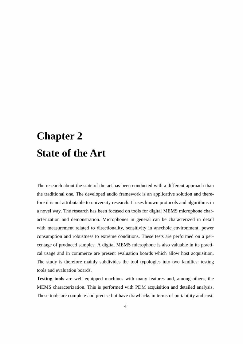
The portability is constrained by the necessity of an external device combined with a host
used for data elaboration. An example is constituted by the Audio Precision. It is a ma-
chine for audio data elaboration and has been recently equipped with PDM acquisition. Its
dimensions are 44.5x46x14 cm and it is therefore a not portable solution. Its calculus ca-
pacity is not required for the evaluation context. The cost of such complex device is obvi-
ously high, in the order of magnitude of millions dollars. The figure visually explains the
equipment structure. It is clear that many functionalities are not related to digital MEMS
microphones and therefore the product cannot be considered an optimized platform.
Figure 1 – Audio Precision
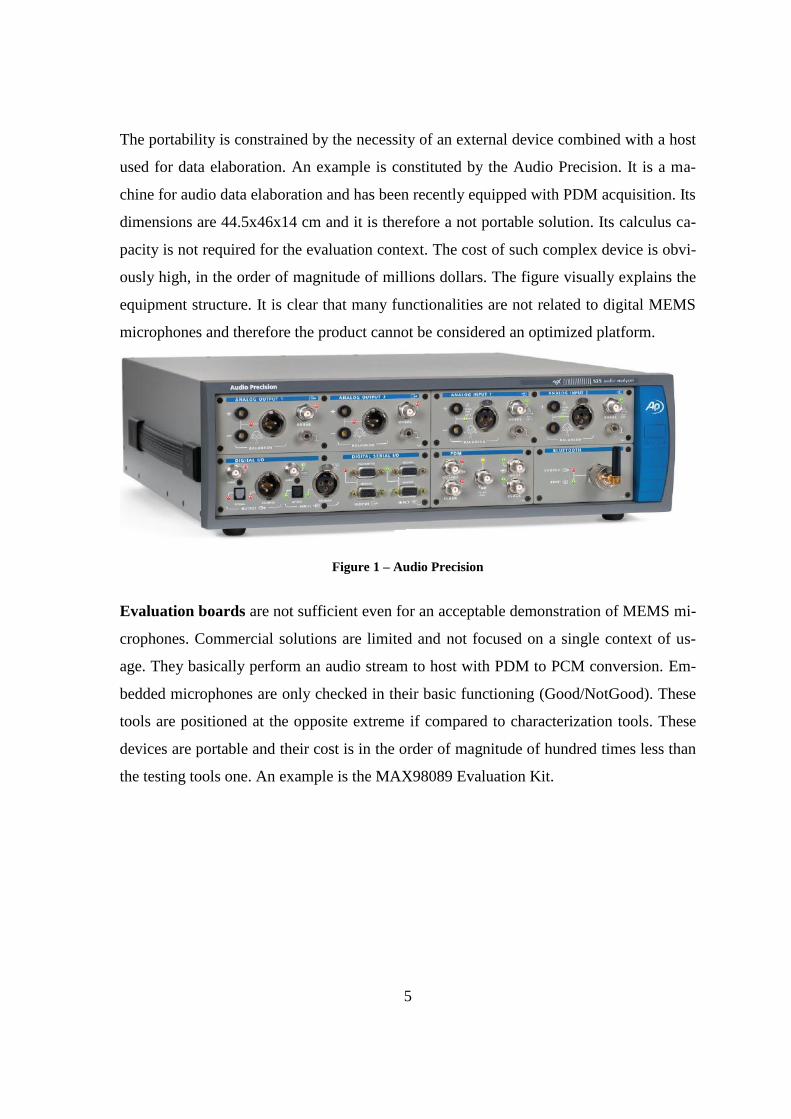
Evaluation boards are not sufficient even for an acceptable demonstration of MEMS mi-
crophones. Commercial solutions are limited and not focused on a single context of us-
age. They basically perform an audio stream to host with PDM to PCM conversion. Em-
bedded microphones are only checked in their basic functioning (Good/NotGood). These
tools are positioned at the opposite extreme if compared to characterization tools. These
devices are portable and their cost is in the order of magnitude of hundred times less than
the testing tools one. An example is the MAX98089 Evaluation Kit.
6
Figure 2 – MAX98089 EVKIT map
This tool has functionalities whose permit a complete audio stream also from a digital mi-
crophone source but no host processing is performed. This is simply a dummy stream for
Good/Not Good microphone test.
The proposed solution starts from an idea which is related to the evaluation context but its
aims is to obtain a quality comparable to testing device tools for functionalities related to
MEMS microphone processing. The host platforms a processing with ad-hoc scenarios
dedicated to each product feature. This is a novel hybrid tool for basic tests and evalua-
tion optimized for digital MEMS microphones.
7
Chapter 3
Development platform
This chapter proposes an overview of the principal framework components characteristics
and their usage in audio applications. Initially is presented a brief introduction about mi-
crocontrollers history, evolution and equipment followed by a focus on STM32F107RC
achievements and reasons connected to its choice in this project.
3.1 Microcontrollers
A Microcontroller is an electronic programmable device that can perform different func-
tionalities autonomously. Essentially it controls a multiplicity of configurable in-
put/output lines in relation with the code which implements. Differently from micropro-
cessors, in MCUs the program code is stored inside a memory area (non-volatile) and it is
run cyclically; inside the same device are present: RAM for volatile data and optionally a
data zone non-volatile and erasable (EEPROM - Electrically Erasable Programmable
Read Only Memory). The input/output stage it is already implemented and some MCUs
have interface for analog signals, comparator or serial communications. A distinctive tract

8
between a MCU and a microprocessor is the autonomy; in fact the first is independent in
its functioning while the second needs external peripherals to work properly (to be com-
pletely operative). MCUs are used especially in applications where computational com-
plexity is not a priority. Moreover a bridge between a single controller and a more power-
ful controller permits to perform the elaboration of information coming from the MCU.
Microcontroller's applications are multiple. MCUs have been used for monitoring and da-
ta recording where the most important features are low power consumption (in idle state)
and the auto-re-activation by interrupts, easily implementable. MCUs are born under the
philosophy of the first model of PLC: integration of a processor core, in an environment
different from that used for general-purpose machine, for resolution of specialized prob-
lems (mainly in Boolean logic). Proto-MCUs structure can be found in microprocessor
such as Zilog Z80, Intel 8088 and the Motorola 6809. Reducing dimensions, all the com-
ponents needed for a controller have been integrated on a single chip giving birth to mod-
ern microcontrollers. The most diffuse construction model is the CMOS which permits
low power usage and battery supply. CMOS chips are quasi-statics, that enable to slow
down the clock frequency (or stop it) until reaching the sleep mode. They are also highly
immune to electro-magnetic noise (supply fluctuation and current peak). MCU, often de-
fined as single-chip solution, is composed by the following components:
Microprocessor at 4, 8, 16, 24 or 32 bit
RAM memory of small dimension, used only for memorize intermediate variables
or input/output variables
EEPROM memory for memorizing the executable program code
I/O peripheral for read or generate signals for which the micro-controller is al-
ready specialized by production (by design).
Added EEPROM memory to memorize non-volatile variables and to preserve
them also after reset
Timers
Module for interrupts control
Other added modules, such as A/D converters, D/A converters, module for serial commu-
nication on bus, and so on
9
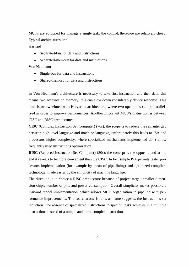
MCUs are equipped for manage a single task: the control, therefore are relatively cheap.
Typical architectures are:
Harvard
Separated-bus for data and instructions
Separated-memory for data and instructions
Von Neumann
Single-bus for data and instructions
Shared-memory for data and instructions
In Von Neumann's architecture is necessary to take first instruction and then data; this
means two accesses on memory: this can slow down considerably device response. This
limit is overwhelmed with Harvard’s architecture, where two operations can be parallel-
ized in order to improve performances. Another important MCU's distinction is between
CISC and RISC architectures:
CISC (Complex Instruction Set Computer) (70s): the scope is to reduce the semantic gap
between high-level language and machine language, unfortunately this leads to ISA and
processors higher complexity, where specialized mechanisms implemented don't allow
frequently used instructions optimization.
RISC (Reduced Instruction Set Computer) (80s): the concept is the opposite and at the
end it reveals to be more convenient than the CISC. In fact simple ISA permits faster pro-
cessors implementation (for example by mean of pipe-lining) and optimized compilers
technology, made easier by the simplicity of machine language.
The direction is to choice a RISC architecture because of project target: smaller dimen-
sion chips, number of pins and power consumption. Overall simplicity makes possible a
Harvard model implementation, which allows MCU organization in pipeline with per-
formance improvements. The last characteristic is, as name suggests, the instructions set
reduction. The absence of specialized instructions to specific tasks achieves in a multiple
instructions instead of a unique and more complex instruction.

10
3.1.1 ARM M3
System-on-chip solutions based on ARM embedded processors address many different
market segments including enterprise applications, automotive systems, home network-
ing, wireless technologies and audio devices. The ARM Cortex™ family of processors
provides a standard architecture to address the broad performance spectrum required by
these diverse technologies. The family includes processors based on the three distinct pro-
files of the ARMv7 architecture; the A profile for sophisticated, high-end applications
running open and complex operating systems; the R profile for real-time systems; and the
M profile optimized for cost-sensitive and microcontroller applications.
Figure 3 – Cortex-M3 processor
The Cortex-M3 processor is the first ARM processor based on the ARMv7-M architec-
ture and has been specifically designed to achieve high system performance in power-
and cost-sensitive embedded applications, such as microcontrollers, automotive body sys-
tems, industrial control systems and wireless networking, while significantly simplifying
programmability to make the ARM architecture an option for even the simplest applica-
tions.
11
3.1.2 STM32
The STM32 is a 32 bit microcontroller family based on ARM Cortex - M3 core. It uses
Harvard architecture for parallel management of instructions as other arm core processors
that allows low power operations and hard real time tasks. These characteristics fit for
audio application based on computationally un-expansive processes where synchroniza-
tion is the priority. The detailed exposition of project requirements is presented at chapter
5.
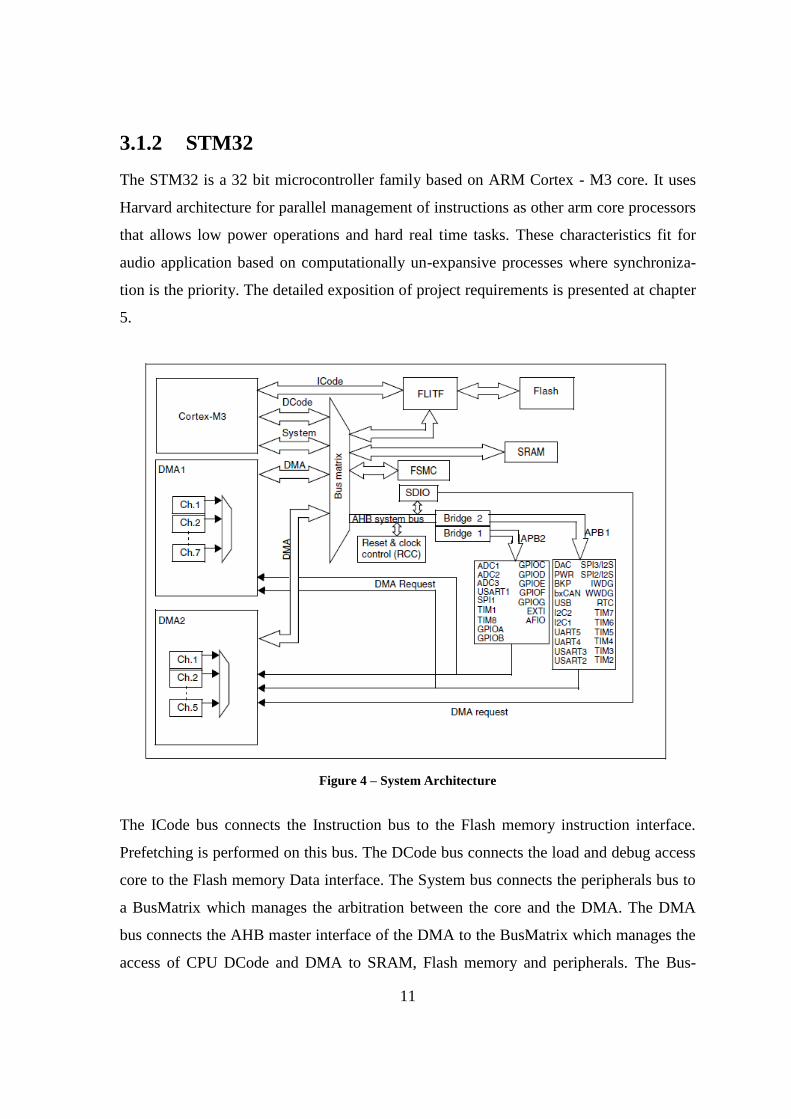
Figure 4 – System Architecture
The ICode bus connects the Instruction bus to the Flash memory instruction interface.
Prefetching is performed on this bus. The DCode bus connects the load and debug access
core to the Flash memory Data interface. The System bus connects the peripherals bus to
a BusMatrix which manages the arbitration between the core and the DMA. The DMA
bus connects the AHB master interface of the DMA to the BusMatrix which manages the
access of CPU DCode and DMA to SRAM, Flash memory and peripherals. The Bus-

12
Matrix manages the access arbitration between the core system bus and the DMA master
bus. The arbitration uses a Round Robin algorithm. In connectivity line devices, the
BusMatrix is composed of five masters (CPU DCode, System bus, Ethernet DMA,
DMA1 and DMA2 bus) and three slaves (FLITF, SRAM and AHB2APB bridges). In
other devices, the BusMatrix is composed of four masters (CPU DCode, System bus,
DMA1 bus and DMA2 bus) and four slaves (FLITF, SRAM, FSMC and AHB2APB
bridges). AHB peripherals are connected on system bus through a BusMatrix to allow
DMA access. The two AHB/APB bridges provide full synchronous connections between
the AHB and the 2 APB buses. APB1 is limited to 36 MHz, APB2 operates at full speed
(up to 72 MHz depending on the device). Differently from first arm architecture, ARM
M3 data access is un-aligned assuring a more efficient usage of internal SRAM. A key
component of STM32 MCU family is the NVIC. The Nested Vector Interrupt Controller
is organized in an interrupt standard structure for microcontroller and exceptional based
interrupt.
Each NVIC dedicated interrupt can be individually prioritized for a maximum number of
240 peripherals. This is a fast system: time elapsed between received interrupt and first
code line execution is 12 cycles. Successive interrupts are performed with 6 cycles thanks
to Tail Chaining feature. STM32 can also be configured to enter in a low power mode af-
ter the interrupt handling routine.
Figure 5 - STM32F10xxx Family
13
STM32 family is subdivided in four different variants, here listed configurations and their
system clock frequency:
Performance line – 72MHz
Access line – 36 MHz
USB Access line – 48MHz
Connectivity line – 72MHz
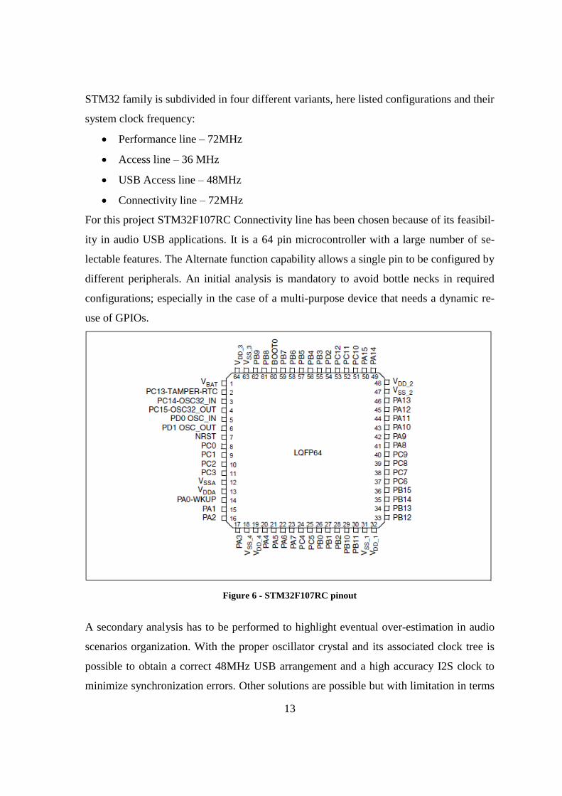
For this project STM32F107RC Connectivity line has been chosen because of its feasibil-
ity in audio USB applications. It is a 64 pin microcontroller with a large number of se-
lectable features. The Alternate function capability allows a single pin to be configured by
different peripherals. An initial analysis is mandatory to avoid bottle necks in required
configurations; especially in the case of a multi-purpose device that needs a dynamic re-
use of GPIOs.
Figure 6 - STM32F107RC pinout
A secondary analysis has to be performed to highlight eventual over-estimation in audio
scenarios organization. With the proper oscillator crystal and its associated clock tree is
possible to obtain a correct 48MHz USB arrangement and a high accuracy I2S clock to
minimize synchronization errors. Other solutions are possible but with limitation in terms

14
of GPIO configurability and computational power.STM32F103xx hasn’t I2S peripheral
except for high-density line. No relevant differences between connectivity line devices for
the utilization in this project.
3.2 Host
The host is the physical block which performs the elaboration on the acquired data. It is
equipped with a visual feedback interface and human interface devices. This allows a
high level of user personalization. Its computational capacity enables features for differ-
ent use cases. Nowadays the host is broadly diffused in any context because of its porta-
bility and reduced costs. For this application there is no need for an excessive computa-
tional capacity. A medium performances host is feasible for all the features that are re-
quired in a real-time audio application. In the proposed project the host will be connected
to a STM32 via USB. It can be seen as a step for the acquisition chain. It is the host which
enables a significant interpretation of the data acquired and a successive perceptual evalu-
ation for the audio framework user.
3.3 Device Under Test
Device Under Test (DUT) means any device connected to the microcontroller bridge in
the audio framework. In order to exploit completely the functionalities of the proposed
platform is needed a compatibility of the device. It has to stream audio with the I2S pro-
tocol from digital MEMS microphones and needs also an I2C communication protocol for
registers configuration. Each ST’s DUT is equipped with a dedicated 16 pins connector
which facilitates and unifies the hardware connection. A DUT example is the
STA321MPL, a processor for digital MEMS microphones acquisition and processing.

15
Chapter 4
Protocols & Coding algorithms
This chapter is an introductive explanation of the standard protocols and coding algo-
rithms implemented. It shows only functionalities which has been relevance in the appli-
cation. This argument will be deepened in the implementation chapter. Adopted protocols
are involved mainly in two operative actions: audio stream and device registers
read/write. Coding algorithms only regard the audio stream digitalization and transporta-
tion, being the tasks with more restrictions in term of synchronization and data loss.
4.1 Protocols
A Communication between two or more electronic devices is achievable with a multiplic-
ity of lines called bus. In order to achieve a correct interaction, a specific communication
protocol becomes necessary. In this paragraph are detailed the selected standards, whose
diffusion in nowadays architecture imply a constraint in their choice for this tool. It fol-
lows I2C, I2S and USB protocols definition.
16
4.1.1 I2C
I2C is a Philips standard which allows information exchange between devices intercon-
nected with a bus composed by two lines, defined SCL and SDA, associated respectively
to clock and data line. Line signals can assume binary values related with supply or
ground voltage. The two lines are set as floating and connected to the supply voltage with
a pull-up resistor. In this way they remain in a state of “weak-high”, easily modifiable by
another device. Each device connected to these lines has a univocal address and is able to
set itself master or slave, according to its capabilities. Master is the transmission starter,
slave is the request receiver. Both two configurations can be arranged as transmitter or re-
ceiver. Transfer mode can be:
A transmits data to B:
A (master) send its address to B (slave) on the bus
A (master-transmitter) transmits data to B (slave-receiver)
A terminates the transfer
A receives data from B:
A (master) sends the B(slave) address on the bus
B (slave-transmitter) transmits data to A (master-receiver)
A terminates the transfer
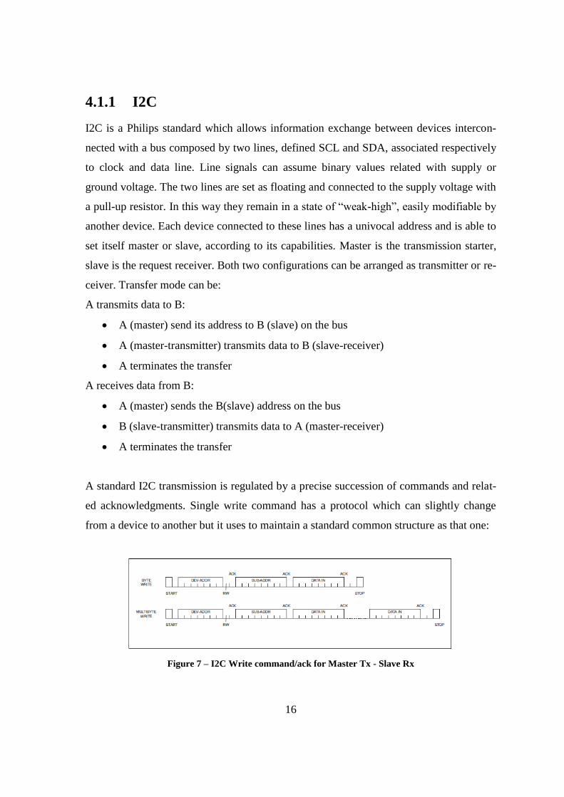
A standard I2C transmission is regulated by a precise succession of commands and relat-
ed acknowledgments. Single write command has a protocol which can slightly change
from a device to another but it uses to maintain a standard common structure as that one:
Figure 7 – I2C Write command/ack for Master Tx - Slave Rx
17
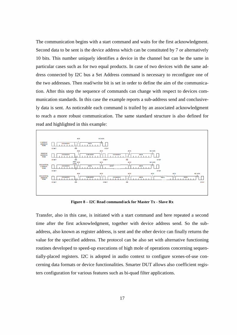
The communication begins with a start command and waits for the first acknowledgment.
Second data to be sent is the device address which can be constituted by 7 or alternatively
10 bits. This number uniquely identifies a device in the channel but can be the same in
particular cases such as for two equal products. In case of two devices with the same ad-
dress connected by I2C bus a Set Address command is necessary to reconfigure one of
the two addresses. Then read/write bit is set in order to define the aim of the communica-
tion. After this step the sequence of commands can change with respect to devices com-
munication standards. In this case the example reports a sub-address send and conclusive-
ly data is sent. As noticeable each command is trailed by an associated acknowledgment
to reach a more robust communication. The same standard structure is also defined for
read and highlighted in this example:
Figure 8 – I2C Read command/ack for Master Tx - Slave Rx
Transfer, also in this case, is initiated with a start command and here repeated a second
time after the first acknowledgment, together with device address send. So the sub-
address, also known as register address, is sent and the other device can finally returns the
value for the specified address. The protocol can be also set with alternative functioning
routines developed to speed-up executions of high mole of operations concerning sequen-
tially-placed registers. I2C is adopted in audio context to configure scenes-of-use con-
cerning data formats or device functionalities. Smarter DUT allows also coefficient regis-
ters configuration for various features such as bi-quad filter applications.
18
4.1.2 I2S
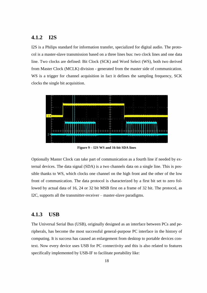
I2S is a Philips standard for information transfer, specialized for digital audio. The proto-
col is a master-slave transmission based on a three lines bus: two clock lines and one data
line. Two clocks are defined: Bit Clock (SCK) and Word Select (WS), both two derived
from Master Clock (MCLK) division - generated from the master side of communication.
WS is a trigger for channel acquisition in fact it defines the sampling frequency, SCK
clocks the single bit acquisition.
Figure 9 – I2S WS and 16-bit SDA lines
Optionally Master Clock can take part of communication as a fourth line if needed by ex-
ternal devices. The data signal (SDA) is a two channels data on a single line. This is pos-
sible thanks to WS, which clocks one channel on the high front and the other of the low
front of communication. The data protocol is characterized by a first bit set to zero fol-
lowed by actual data of 16, 24 or 32 bit MSB first on a frame of 32 bit. The protocol, as
I2C, supports all the transmitter-receiver – master-slave paradigms.
4.1.3 USB
The Universal Serial Bus (USB), originally designed as an interface between PCs and pe-
ripherals, has become the most successful general-purpose PC interface in the history of
computing. It is success has caused an enlargement from desktop to portable devices con-
text. Now every device uses USB for PC connectivity and this is also related to features
specifically implemented by USB-IF to facilitate portability like:
19
Micro-USB
On-The-Go
Battery Charging
Embedded Host
The USB is a polled bus. Each transaction begins when the Host Controller, on a sched-
uled basis, sends a USB packet describing the type and direction of transaction, the USB
device address, and endpoint number. This packet is referred to as the “token packet”.
The USB device that is addressed selects itself by decoding the appropriate address fields.
In a given transaction, data is transferred either from the host to a device or from a device
to the host. The direction of data transfer is specified in the token packet. The source of
the transaction then sends a data packet or indicates it has no data to transfer. The destina-
tion, in general, responds with a handshake packet indicating whether the transfer was
successful. The USB data transfer model between a source or destination on the host and
an endpoint on a device is referred to as a pipe. There are two types of pipes: stream and
message. Stream data has no USB-defined structure, while message data does. Addition-
ally, pipes have associations of data bandwidth, transfer service type, and endpoint char-
acteristics like directionality and buffer sizes. Most pipes come into existence when a
USB device is configured. One message pipe, the Default Control Pipe, always exists
once a device is powered, in order to provide access to the device’s configuration, status,
and control information. The transaction schedule allows flow control for some stream
pipes. At the hardware level, this prevents buffers from under-run or over-run situations
by using a NAK handshake to throttle the data rate. If NAK-ed, a transaction is retried
when bus time is available. The flow control mechanism permits the construction of flex-
ible schedules that accommodate concurrent servicing of a heterogeneous mix of stream
pipes. Thus, multiple stream pipes can be serviced at different intervals and with packets
of different sizes. USB data transfers take place between host software and a particular
endpoint on a USB device. Such associations between the host software and a USB de-
vice endpoint are called pipes. In general, data movement though one pipe is independent
from the data flow in any other pipe. A given USB device may have many pipes. As an
example, a given USB device could have an endpoint that supports a pipe for transporting

20
data to the USB device and another endpoint that supports a pipe for transporting data
from the USB device. The USB architecture comprehends four basic types of data trans-
fers:
Control Transfers Used to configure a device at attach time and can be used for other
device-specific purposes, including control of other pipes on the device.
Bulk Data Transfers Generated or consumed in relatively large and bursty quantities and
have wide dynamic latitude in transmission constraints.
Interrupt Data Transfers Used for timely but reliable delivery of data, for example,
characters or coordinates with human-perceptible echo or feedback response characteris-
tics.
Isochronous Data Transfers Occupy a pre-negotiated amount of USB bandwidth with a
pre-negotiated delivery latency, (also called streaming real time transfers).
Devices connected via USB are logically differentiated by interface classes and associat-
ed functions. Every USB peripheral is configurable with respect to its usage. The de-
scriptor is a declaration method that the device uses to show its interface class, and con-
sequentially related features, to the host side. Let’s now introduce the classes concerning
this activity.
Audio Class
The Audio Device Class Definition applies to all devices or functions embedded in com-
posite devices that are used to manipulate audio, voice, and sound-related functionality.
This includes both audio data and the functionality that is used to directly control the au-
dio environment, such as volume and tone control. Audio data descriptors for audio
streaming are composed of minimum two interfaces. One is the standard interface which
operates as a controller for the audio streaming, the other actually performs audio data
stream. The audio streaming interface configures endpoint directions for each simultane-
ous stream required. For a complete audio stream one endpoint is necessary, in fact each
endpoint is defined for two directions. Audio endpoints are shaped as isochronous end-
points which can be further configured with respect to synchronization policy.
21
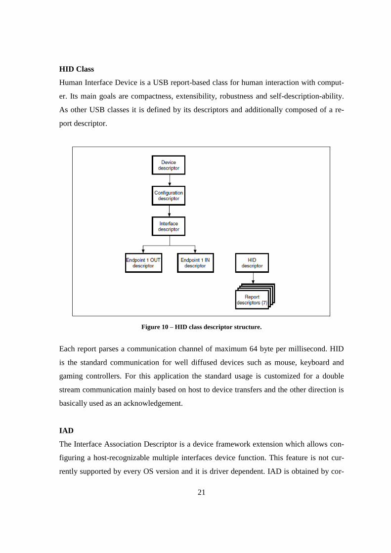
HID Class
Human Interface Device is a USB report-based class for human interaction with comput-
er. Its main goals are compactness, extensibility, robustness and self-description-ability.
As other USB classes it is defined by its descriptors and additionally composed of a re-
port descriptor.
Figure 10 – HID class descriptor structure.
Each report parses a communication channel of maximum 64 byte per millisecond. HID
is the standard communication for well diffused devices such as mouse, keyboard and
gaming controllers. For this application the standard usage is customized for a double
stream communication mainly based on host to device transfers and the other direction is
basically used as an acknowledgement.
IAD
The Interface Association Descriptor is a device framework extension which allows con-
figuring a host-recognizable multiple interfaces device function. This feature is not cur-
rently supported by every OS version and it is driver dependent. IAD is obtained by cor-

22
rectly configuring the multi interface device descriptors on a host. This additional de-
scriptor is mandatory for each device function requiring more than one interface.
Figure 11 – IAD descriptor
Interface association descriptor includes function class, subclass and protocol fields. Val-
ues in these fields can be the same as the interface class, subclass and protocol values
from any one of the associated interfaces. A preferable implementation, for existing de-
vice classes, is to use the interface class, subclass and protocol field values from the first
interface in the list of associated interfaces.
DFU Class
The DFU class uses USB as a communication channel between the microcontroller and
the programming tool, generally a PC host. The DFU class specification states that, all the
commands, status and data exchanges have to be performed through Control Endpoint
0.The command set, as well as the basic protocol are also defined, but the higher level
protocol (data format, error message etc.) remain vendor-specific. This means that the
DFU class does not define the format of the data transferred (.s19, .hex, pure binary
etc.).Because it is impractical for a device to concurrently perform both DFU operations
and its normal runtime activities, those normal activities must cease for the duration of
the DFU operations. Doing so means that the device must change its operating mode; that
is, a printer is not a printer while it is undergoing a firmware upgrade; it is a
Flash/Memory programmer. However, a device that supports DFU is not capable of
changing its mode of operation on its own volition. External (human or host operating
system) intervention is required. There are four distinct phases required to accomplish a
firmware upgrade:
23
Enumeration The device informs the host of its capabilities. A DFU class-interface de-
scriptor and associated functional descriptor embedded within the device’s normal run-
time descriptors serve this purpose and provide a target for class-specific requests over
the control pipe.
DFU Enumeration The host and the device agree to initiate a firmware upgrade. The
host issues a USB reset to the device, and the device then exports a second set of de-
scriptors in preparation for the Transfer phase. This deactivates the run-time device driv-
ers associated with the device and allows the DFU driver to reprogram the device’s firm-
ware unhindered by any other communications traffic targeting the device.
Transfer The host transfers the firmware image to the device. The parameters specified
in the functional descriptor are used to ensure correct block sizes and timing for pro-
gramming the non-volatile memories. Status requests are employed to maintain synchro-
nization between the host and the device.
Manifestation Once the device reports to the host that it has completed the reprogram-
ming operations, the host issues a USB reset to the device. The device re-enumerates and
executes the upgraded firmware. To ensure that only the DFU driver is loaded, it is con-
sidered necessary to change the id-Product field of the device when it enumerates the
DFU descriptor set. This ensures that the DFU driver will be loaded in cases where the
operating system simply matches the vendor ID and product ID to a specific driver.
4.2 Coding algorithms
This paragraph concerns about coding algorithms adopted in the device digital audio
stream. Audio digital solution requires avoiding loss of information, in particular if per-
ceivable by human ear. In this project digital MEMS microphones acquisition is per-
formed with a PDM coding and a successive conversion to PCM. Another possibility
concerns I2S acquisition of a PCM audio stream over USB: PCM signal is acquired loss-
less, synchronization of USB channel is lossy. USB synchronization issue will be faced in
the implementation chapter.

24
4.2.1 PDM - Pulse Density Modulation
Pulse density modulation, or PDM, is a coding algorithm used to represent an analog sig-
nal in the digital domain. In a PDM signal, specific amplitude values are not encoded into
pulses as they would be in PCM. Instead it is the relative density of the pulses that corre-
sponds to the analog signal's amplitude. To get the framed data from the PDM bit stream,
decimation filters are usually used. The first stage of decimation is used to reduce the
sampling frequency, followed by a high pass filter to remove the signal DC offset.
Figure 12 – PDM coded sinusoid
The figure represents an example of how PDM quantizes an analog sinusoidal signal to
digital binary data. With a binary decisional level the amplitude discretization is exploited
also in the time domain.
4.2.2 PCM - Pulse Code Modulation
The majority of digital recording systems have essentially the same function mechanism:
An audio signal is acquired by an Analog-to-Digital converter which samples the source
signal at fixed time interval and memorizes it as a number. The numbers sequence is then

25
stored in a support and become available for playback. The Pulse Code Modulation is a
technique to code an analog signal in a digital form. A digital representation of an analog
signal passes through a discretization stage that is performed in time and amplitude. Time
discretization is performed by sampling. Amplitude discretization is performed by quanti-
zation.
Figure 13 – PAM sampling

26
Chapter 5
Specification & Requirements
This chapter explains the main idea behind this work, born from a real need related to au-
dio analysis context, and consequentially the characteristics derived from its prototyping.
It is now important to define basic differences between a testing/characterization and a
demonstration/evaluation tool. Evaluation is a qualitative and not detailed analysis of a
device. It yields to direct vast-scale appreciable evidences and focuses on a particular as-
pect or on a standard functionality. Characterization is a detailed and quantitative analysis
of a device. Its numerically-based test evidences necessary and sufficient conditions for a
device to be completely defined in all its usage aspects. The project target is the creation
of an audio framework focused on perspective analysis aspects. From requirements is not
equipped with fine measurement functionalities but its host-device approach allows flexi-
bility and future work can be the creation of an optimized tool. This evidences a hybrid
utilization which cannot be easily compared with audio interfaces present in literature. A
research about the state of the art of characterization and evaluation devices put in evi-
dence fundamental points that became useful for focus on needed capabilities. Four main
27
aspects emerge between the others for the definition of the system: portability, scalability,
reliability and cost are the abstract characteristics that fit the project requirements. Here
follows an elucidation regarding the novel prototype specifications.
5.1 Portability
Starting from fundamental, hardware is the first constraint and dimension is a priority.
The planned tool is required to explore others scenarios if compared to its predecessors.
Advanced audio testing solutions have not been optimized in dimensions but only in test-
ing quality: Evaluation devices are not specialized on a single context of use. They are
equipped with lot of peripherals and therefore not optimized in their portability. The tar-
get of this project is a multi-purpose easily-transportable device with digital performances
and usable in contexts such as customer demonstrations, exhibitions or congresses.
MEMS microphones are, in this way, valuable in their qualitative behavior, a sufficient
condition to demonstrate their practical usage capabilities.
5.2 Scalability
Scalability is an imperative in a multi-purpose tool realization. The presented device is
focused in audio streaming and, starting from this scenario, it opens a multiplicity use
cases and configurations. Scalability is related to different ambits of this project:
OS Compatibility cannot be leaved out consideration. The system is requested to be usa-
ble on a diffused operative system. Due to the USB multi-function descriptor policy cho-
sen, only Microsoft OSs family compatibility is assured. This is related to IAD de-
scriptors whose driver predispositions are present in Windows versions from Service
Pack 3. Other OSs compatibility is not requested and unnecessary for its actual usage.
Supported sampling frequencies The Framework supports stereo acquisition/emission
of different frequencies and data formats. Acquisition specification defines the following
sampling frequencies for stream in:
16kHz
44.1kHz
48kHz

28
For stream out only 48kHz has been implemented in this framework version and exten-
sion to other frequencies is feasible. This output configuration has been chosen because it
is a standard in audio and, differently from 44.1kHz, has less synchronization constraint.
Boot configurations Hardware and Firmware structure has to permit switching to differ-
ent scenarios for each reboot. Different configurations are better explained in firmware
design chapter. This target is achieved through a dedicated initialization structure which
refers itself to an external memory used to configure the firmware at each reset. The audio
configurations are visible on the following table:
Configuration Name Configuration Features
PDM Capture PDM on-board microphones acquisition
I2S Control I2S Stream-in Slave Receiver
I2C bridge via HID
PDM - I2S Control
PDM on-board microphones acquisition
I2S Stream-out Master Transmitter
I2C bridge via HID
I2S Full-Digital Control
I2S Stream-out Master Transmitter
I2S Stream-in Slave/Master Receiver
I2C bridge via HID
Table 1 - Audio HUB Specifications
As noticeable the suffix Control underlined the presence of the I2C bridge via HID to al-
low dynamic configuration of DUT registers and increment the firmware scalability.
Firmware upgrade via USB. To look forward at future implementations a DFU based
upgradable firmware solution has been chosen. This is obtained thanks to a friendly user
interface used to upload new firmware versions without effort or specialized tools. A
mandatory equipment for in-circuit programming.
Standard Protocols. The multiplicity of connectable audio devices imposes the usage of
standard protocols. In this case the requirement is over-imposed and not debatable. For
digital audio stream I2S has been chosen with 16 bit data. I2C is the selected standard,

29
from the 80s, for devices communication. USB is more than a standard for device-host
data exchange.
DUT compatibility. The board is required to be equipped with a standard 8x2 pins con-
nector which is adopted by a large quantity of ST’s DUT . In fact a practical plug-and-
play connector avoids personalized hardware modifications and allows a smart utilization.
This standard regards only ST Microelectronics board for amplification and microphone
evaluation and processing.
5.3 Reliability & Performance
Mandatory characteristics of an evaluation tool are reliability and performance. A mean
to obtain an high quality stream without error proliferation or expansive and complex
equipment is digitalization. Digital conversion in MEMS microphone is based on PDM
coding acquisition which takes place in the ASIC, an ADC integrated inside the micro-
phone structure. This acquisition guarantees a quasi-digital-quality chain if the signal
emitted for acquisition is digital and ideally streamed by linear response speakers in ane-
choic environment. Therefore the quality purpose is to obtain a perceptively lossless data
stream to suppress unnecessary channel noise. A Digital stream is differentiable by the
channel transfer protocol. The specification has defined I2S because it represents a stand-
ard in this field, influenced by hub compatibility with other devices.
Full Digital The actual realization of the above requirement is expressed by the Full Digi-
tal feature. Such capability allows a device to be generation and acquisition tool in a sin-
gle solution. This implies double audio stream supportability and a complete synchroniza-
tion between the two directions streams.
5.4 Cost
Cost is always a parameter to be considered for actual prototype realization. In the partic-
ular case, this requirement is a consequence of the previous ones. The initial choice of a
microcontroller pulls down material costs in favor to a higher cost/performance ratio. As
highlighted by the Chapter 2 there is an enormous gap in terms of price between a testing
tool compared and an evaluation board. The singularity of the proposed audio framework

30
is related to an actual testing behavior created in an evaluation environment. It is not pos-
sible to sustain that the audio framework is equal to a testing machine but the platform
can substitute it partially in this context of use.
31
Chapter 6
Implementation
As every realizable project imposes the definition of requirements is followed by imple-
mentation. Priority here becomes the design and the choice of right technologies to put
into practice the work specifications. This chapter is subdivided in design and develop-
ment of the project structures. The design introduces the hardware prototype from which
the whole system realization starts. The second step is represented by the firmware design
strictly connected to the device limitation and capabilities. Finally the host-side definition
of software tool to complete the framework composition. The development phase focuses
principally on the actual blocking points and their resolution policies.
6.1 Device Design
The STM32F107RC connectivity line, as previously described, well suits requirements
for this project thanks to its performances and adaptability.
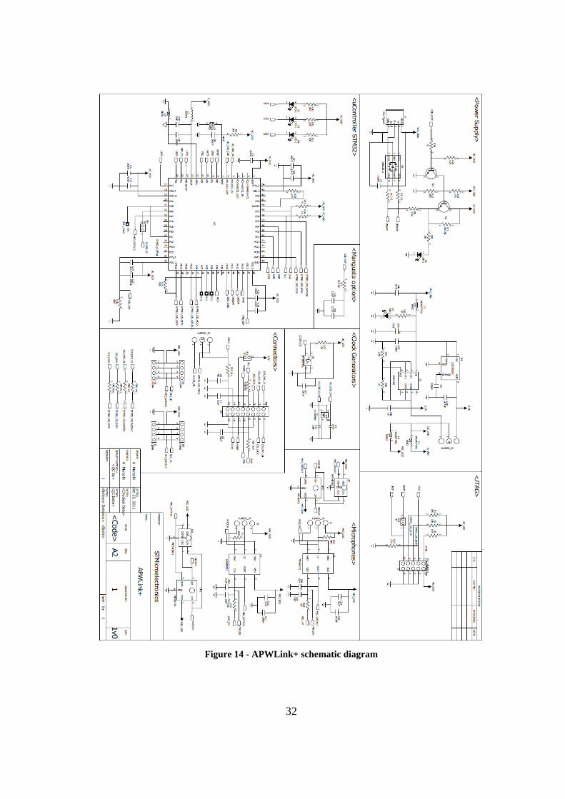
32
Figure 14 - APWLink+ schematic diagram
33
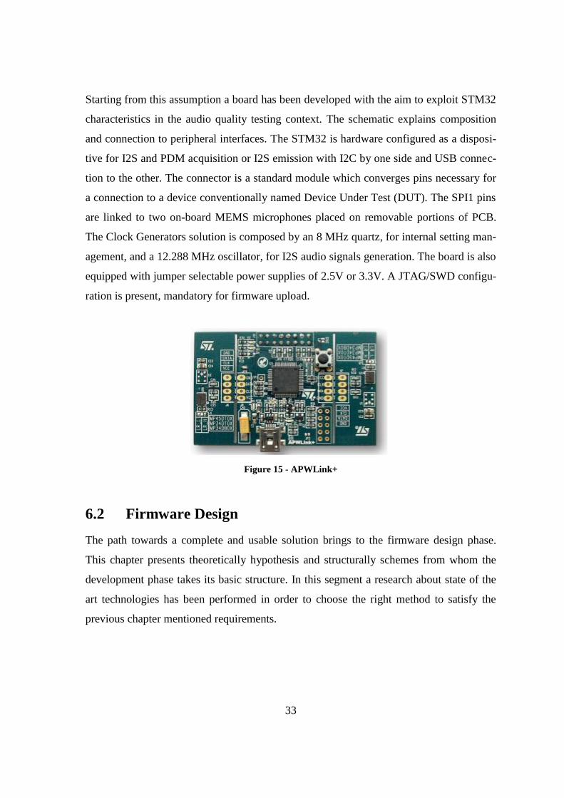
Starting from this assumption a board has been developed with the aim to exploit STM32
characteristics in the audio quality testing context. The schematic explains composition
and connection to peripheral interfaces. The STM32 is hardware configured as a disposi-
tive for I2S and PDM acquisition or I2S emission with I2C by one side and USB connec-
tion to the other. The connector is a standard module which converges pins necessary for
a connection to a device conventionally named Device Under Test (DUT). The SPI1 pins
are linked to two on-board MEMS microphones placed on removable portions of PCB.
The Clock Generators solution is composed by an 8 MHz quartz, for internal setting man-
agement, and a 12.288 MHz oscillator, for I2S audio signals generation. The board is also
equipped with jumper selectable power supplies of 2.5V or 3.3V. A JTAG/SWD configu-
ration is present, mandatory for firmware upload.
Figure 15 - APWLink+
6.2 Firmware Design
The path towards a complete and usable solution brings to the firmware design phase.
This chapter presents theoretically hypothesis and structurally schemes from whom the
development phase takes its basic structure. In this segment a research about state of the
art technologies has been performed in order to choose the right method to satisfy the
previous chapter mentioned requirements.

34
6.2.1 Clock Tree
The choice of the clock tree is fundamental for firmware implementation. It can limit the
possibility of STM32 usage. For this project three implementations have been analyzed.
Initially STM32 was equipped with two clock generators. An 8MHz quartz and a
12.288MHz oscillator. The first is essentially a frequency which permits multiple config-
urations; the second one is an audio frequency: a standard for I2S master clock, suitable
to generate a stable audio acquisition/emission in slave mode.
Figure 16 - clock tree 8MHz scheme
The above setting doesn't fit well for USB audio stream if the STM32 it is configured as a
master generator. An 8MHz quartz doesn't allow to configure a clock tree with sufficient
accuracy on the I2S side. As emphasized by the table below the 8MHz reaches a low lev-
el of accuracy in the generation of the communication clocks with consequently draw-
backs in USB synchronization. Standard audio sampling frequencies, such as 48kHz or
44,1kHz are not represented with the adequate level of precision. This problem can be
overwhelmed with the synchronization policies presented in the third paragraph but it
brings inevitably to a higher rate of rejected samples.

35
Figure 17 - table 8MHz quartz
For an optimal I2S audio + USB connection, the STM32 data-sheet recommends
14.7456MHz quartz solution. In fact in this case is possible to reach an higher range of
frequencies with better accuracy improving firmware scalability.
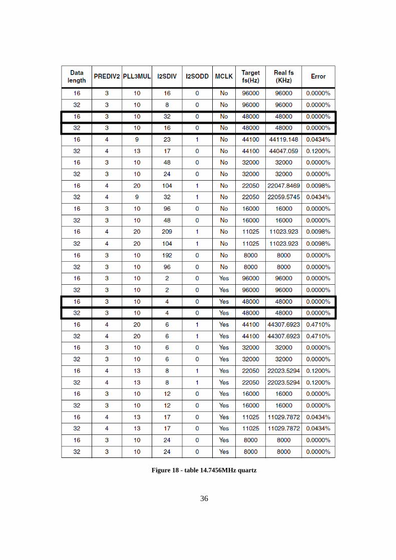
36
Figure 18 - table 14.7456MHz quartz
37
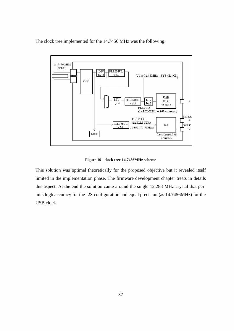
The clock tree implemented for the 14.7456 MHz was the following:
Figure 19 - clock tree 14.7456MHz scheme
This solution was optimal theoretically for the proposed objective but it revealed itself
limited in the implementation phase. The firmware development chapter treats in details
this aspect. At the end the solution came around the single 12.288 MHz crystal that per-
mits high accuracy for the I2S configuration and equal precision (as 14.7456MHz) for the
USB clock.

38
Figure 20 - clock tree 12.288MHz scheme
6.2.2 Audio State Machine
As lots of other control embedded systems, functionalities and architecture of this firm-
ware let themselves easily to a reactive system based on state machine modeling. The de-
vice has a number of defined states and based on events which are input commands it
changes its state to another. As already introduced, the most complex task in the project is
related to the audio streaming and in order to reduce its complexity, a state machine ap-
proach has been implemented. Solution provided is based on two state machines transver-
sally operative on different levels.
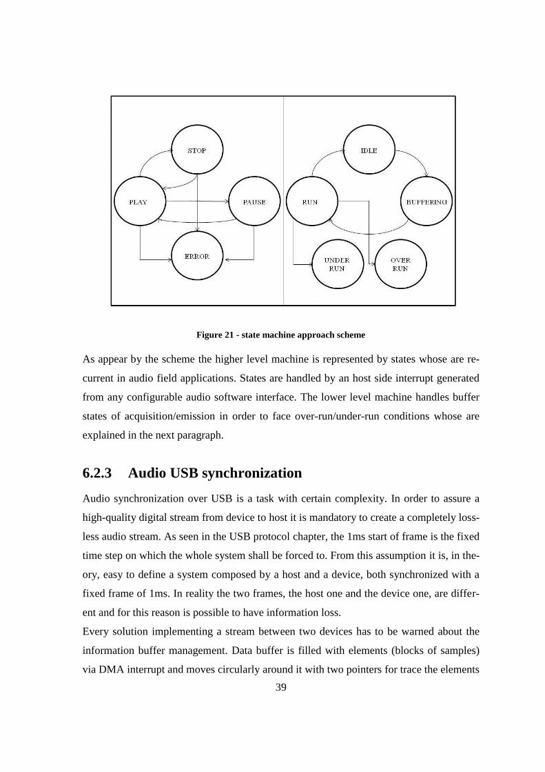
39
Figure 21 - state machine approach scheme
As appear by the scheme the higher level machine is represented by states whose are re-
current in audio field applications. States are handled by an host side interrupt generated
from any configurable audio software interface. The lower level machine handles buffer
states of acquisition/emission in order to face over-run/under-run conditions whose are
explained in the next paragraph.
6.2.3 Audio USB synchronization
Audio synchronization over USB is a task with certain complexity. In order to assure a
high-quality digital stream from device to host it is mandatory to create a completely loss-
less audio stream. As seen in the USB protocol chapter, the 1ms start of frame is the fixed
time step on which the whole system shall be forced to. From this assumption it is, in the-
ory, easy to define a system composed by a host and a device, both synchronized with a
fixed frame of 1ms. In reality the two frames, the host one and the device one, are differ-
ent and for this reason is possible to have information loss.
Every solution implementing a stream between two devices has to be warned about the
information buffer management. Data buffer is filled with elements (blocks of samples)
via DMA interrupt and moves circularly around it with two pointers for trace the elements
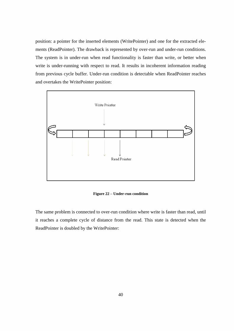
40
position: a pointer for the inserted elements (WritePointer) and one for the extracted ele-
ments (ReadPointer). The drawback is represented by over-run and under-run conditions.
The system is in under-run when read functionality is faster than write, or better when
write is under-running with respect to read. It results in incoherent information reading
from previous cycle buffer. Under-run condition is detectable when ReadPointer reaches
and overtakes the WritePointer position:
Figure 22 – Under-run condition
The same problem is connected to over-run condition where write is faster than read, until
it reaches a complete cycle of distance from the read. This state is detected when the
ReadPointer is doubled by the WritePointer:

41
Figure 23 – Over-run condition
Plus-Minus. The plus-minus algorithm fronts the above described problem with a host-
side correction approach. USB protocol is natively implemented with this defined and not
configurable routine. The only way to active/deactivate plus-minus algorithm is by de-
scriptor endpoint declaration. USB isochronous endpoints can be set with four different
synchronization policies:
0x01: No Synchronization
0x05: Asynchronous
0x09: Adaptive
0x0D: Synchronous
In synchronous configuration host awaits to receive a fixed number of data packet for
each transaction. In no synchronization or adaptive method host is able to receive plus or
minus one sample with respect to the average packet dimension. It results in a effective
correction of buffer over-run/under-run blocking point. This algorithm is mandatory for
un-precise frequencies, for example in 44.1kHz streaming management. The drawback is
constituted by its black block approach. In fact host accepts one sample more/less but for
a correct sampling has to actually acquire a fixed number of samples; this implies a not

42
modifiable data interpolation. In order to get round of this limitation a firmware side algo-
rithm is developed.
Add-Remove. The idea behind add/remove algorithm is a device-side preventive correc-
tion with the aim of limit the distance between the two pointers. The solution acts on the
ReadPointer position. The pointer is moved by a step over/under of one sample in order to
be not perceivable. The algorithm is activated by a threshold limit composed by the dis-
tance between the two pointers linearly unrolled. This threshold is related to the single
USB packet dimension:
It is equal to three times the single packet for the activation of the step over and two times
for the step under. In order to make the response smoother an adaptive action is adopted
which starts with a slow correction that can become stronger for distances near to the crit-
ical state. Sample removing with low recurrence is theoretically expected to be not per-
ceivable by human ear. This is not true in practice, so a sharper removing mechanism
based on zero detection has been implemented and documented in the development and
testing paragraphs related to this point.
Feedback Pipe. Feedback pipe is a USB synchronization method related to stream out.
The cost in term of device resources is higher than other methodologies previously faced.
In fact it needs an additional endpoint configured as isochronous feedback to operate cor-
rectly. The choice affects the USB class configuration selected for I2C bridge as deep-
ened in USB HID/Audio IAD paragraph. Additional endpoint necessity is clear: the num-
ber of samples transferred from host to device cannot be manipulated at the device side
because of constraints in time and computation. So, as in plus/minus algorithm, the host
manages this complication. Feedback endpoint communicates the channel samples num-
ber in order to prevent over/under-run critical conditions detected at device-side.
43
6.2.4 PDM acquisition
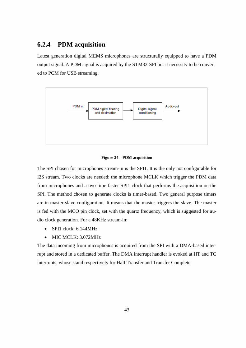
Latest generation digital MEMS microphones are structurally equipped to have a PDM
output signal. A PDM signal is acquired by the STM32-SPI but it necessity to be convert-
ed to PCM for USB streaming.
Figure 24 – PDM acquisition
The SPI chosen for microphones stream-in is the SPI1. It is the only not configurable for
I2S stream. Two clocks are needed: the microphone MCLK which trigger the PDM data
from microphones and a two-time faster SPI1 clock that performs the acquisition on the
SPI. The method chosen to generate clocks is timer-based. Two general purpose timers
are in master-slave configuration. It means that the master triggers the slave. The master
is fed with the MCO pin clock, set with the quartz frequency, which is suggested for au-
dio clock generation. For a 48KHz stream-in:
SPI1 clock: 6.144MHz
MIC MCLK: 3.072MHz
The data incoming from microphones is acquired from the SPI with a DMA-based inter-
rupt and stored in a dedicated buffer. The DMA interrupt handler is evoked at HT and TC
interrupts, whose stand respectively for Half Transfer and Transfer Complete.
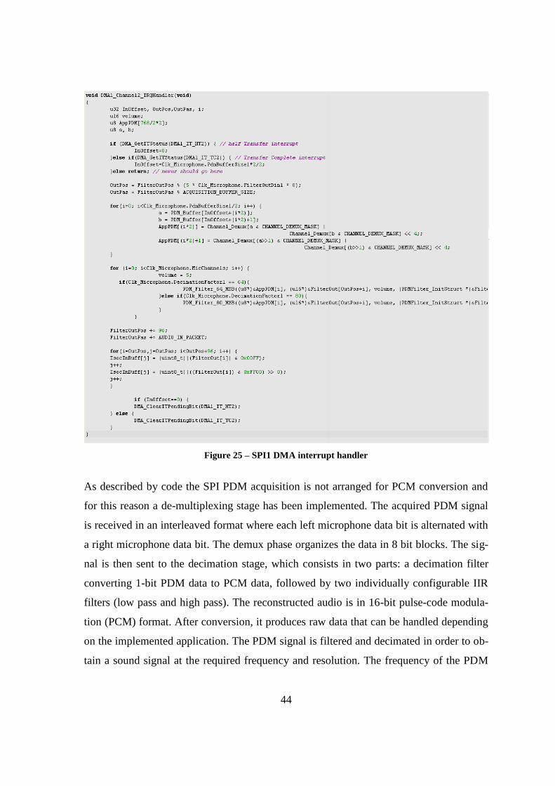
44
Figure 25 – SPI1 DMA interrupt handler
As described by code the SPI PDM acquisition is not arranged for PCM conversion and
for this reason a de-multiplexing stage has been implemented. The acquired PDM signal
is received in an interleaved format where each left microphone data bit is alternated with
a right microphone data bit. The demux phase organizes the data in 8 bit blocks. The sig-
nal is then sent to the decimation stage, which consists in two parts: a decimation filter
converting 1-bit PDM data to PCM data, followed by two individually configurable IIR
filters (low pass and high pass). The reconstructed audio is in 16-bit pulse-code modula-
tion (PCM) format. After conversion, it produces raw data that can be handled depending
on the implemented application. The PDM signal is filtered and decimated in order to ob-
tain a sound signal at the required frequency and resolution. The frequency of the PDM
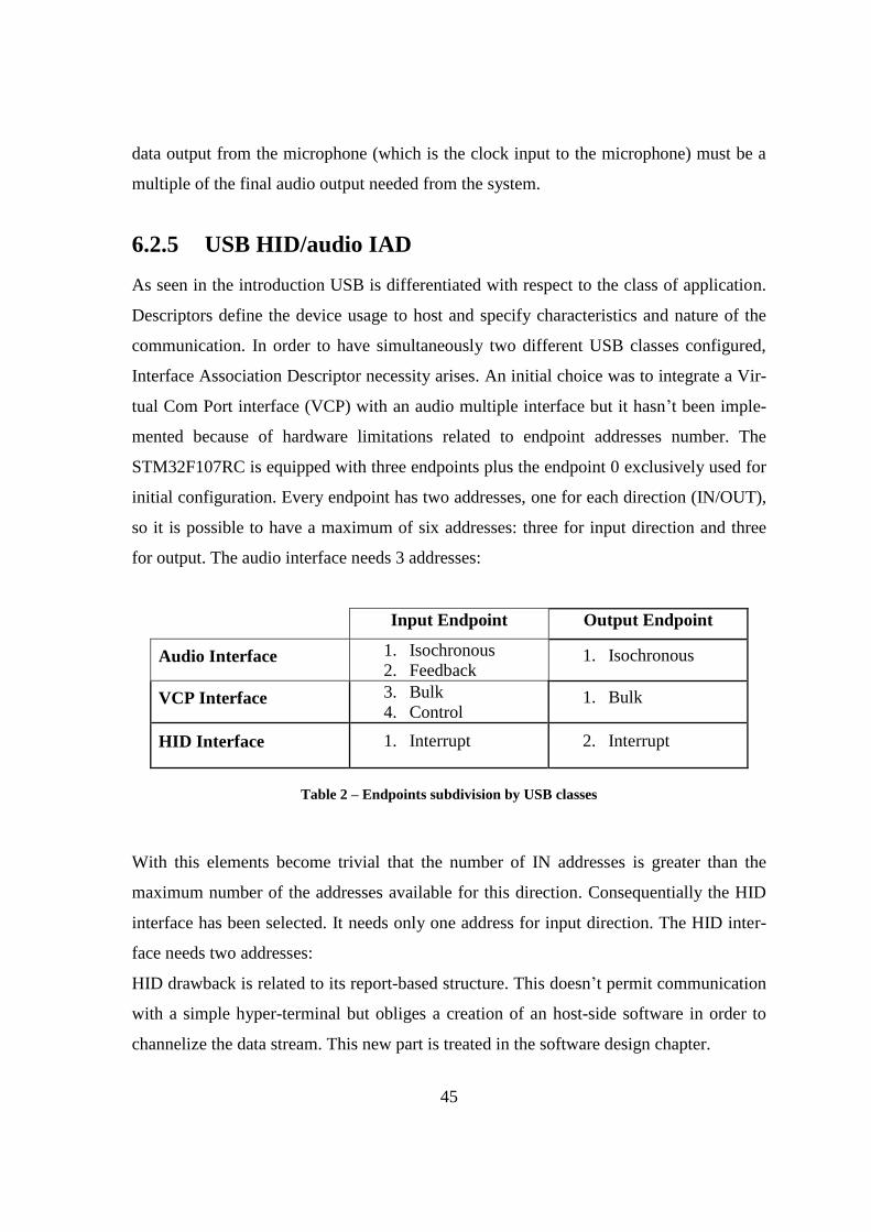
45
data output from the microphone (which is the clock input to the microphone) must be a
multiple of the final audio output needed from the system.
6.2.5 USB HID/audio IAD
As seen in the introduction USB is differentiated with respect to the class of application.
Descriptors define the device usage to host and specify characteristics and nature of the
communication. In order to have simultaneously two different USB classes configured,
Interface Association Descriptor necessity arises. An initial choice was to integrate a Vir-
tual Com Port interface (VCP) with an audio multiple interface but it hasn’t been imple-
mented because of hardware limitations related to endpoint addresses number. The
STM32F107RC is equipped with three endpoints plus the endpoint 0 exclusively used for
initial configuration. Every endpoint has two addresses, one for each direction (IN/OUT),
so it is possible to have a maximum of six addresses: three for input direction and three
for output. The audio interface needs 3 addresses:
Input Endpoint Output Endpoint
Audio Interface 1. Isochronous
2. Feedback 1. Isochronous
VCP Interface 3. Bulk
4. Control 1. Bulk
HID Interface 1. Interrupt 2. Interrupt
Table 2 – Endpoints subdivision by USB classes
With this elements become trivial that the number of IN addresses is greater than the
maximum number of the addresses available for this direction. Consequentially the HID
interface has been selected. It needs only one address for input direction. The HID inter-
face needs two addresses:
HID drawback is related to its report-based structure. This doesn’t permit communication
with a simple hyper-terminal but obliges a creation of an host-side software in order to
channelize the data stream. This new part is treated in the software design chapter.

46
6.2.6 Eeprom/RAM reboot
A single firmware to be multi-purpose needs a re-use of peripherals and GPIOs. Re-
configuration can be arranged by rebooting via software handled reset. This approach is
usable only in contexts that allow memory for previous information storage. Eeprom
memory is used for this scope but STM32 is not equipped with it because of low-cost
purposes. Instead, it is equipped with a Flash memory. The concept is to create an
Eeprom emulator on the Flash to store and recover the firmware configuration at every
start-up.
Figure 26 – Eeprom vs Emulated Eeprom
For single feature modifications is possible to perform changes in firmware and store
them in an un-initialized zone of RAM to obtain a reboot for the following current-
supplied reset. The different bootable configurations are selected from an init-structure.
At every boot an interrogation is performed and firmware redirects its path extracting
from a dedicated marker the RAM, NVM or default configuration.
6.2.7 DFU
For a complete scalability the target is to obtain a solution based on a USB upgradable
firmware, where normally SWD/JTAG-link is required. DFU is the needed interface. In
fact the same USB connector can be used for both the standard operating mode and the

47
reprogramming process. The DFU process, like any other IAP process, is based on the
execution of firmware located in one small portion of the Flash memory. DFU manages
erase and program operations of others Flash memory modules depending on the device
capabilities.
6.3 Software Design
Software has a key role in the project because its function is to exploit information pro-
vided by the device, which actually acts as a communication bridge. Software design has
been planned with a divide-et-impera approach where each system block is developed for
a different device feature. The structure converges then in a unique solution which col-
lects all the framework functionalities.
The three main blocks defined to use audio framework features are:
HID communication
Audio generation/acquisition
DFU management
HID. Communication at host side is exploited with a software structure composed of
three layers. The graphic layer called Report View acts as a front end to trigger user ac-
tions. The USB layer presents APIs to configure USB communication and functions for
read/write operations. The middle layer implements functions used for communication
between the other two in order to facilitate the successive migration/integration.
Audio generation/acquisition. It can be performed by any feasible audio streaming
software. During firmware testing phase Audacity has been used as audio streaming tool,
a well-equipped freeware tool. For audio, the target is to create a personal interface dif-
ferentiate for each DUT, different from usual audio acquisition/generation tool.
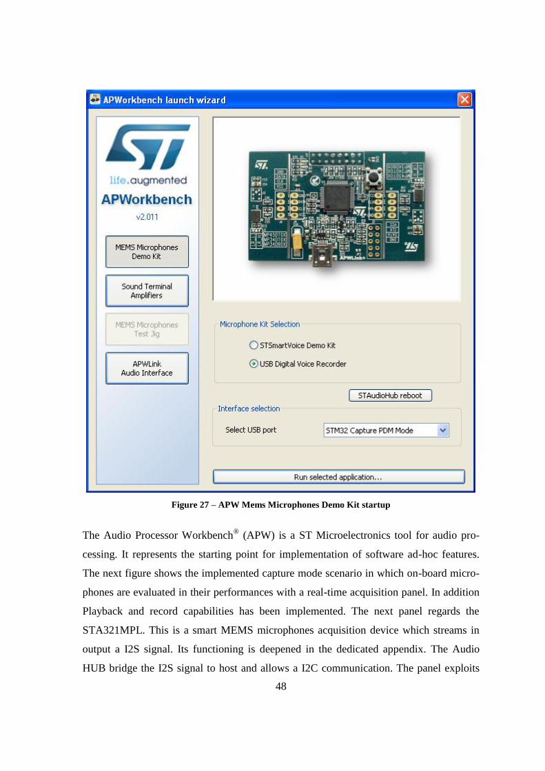
48
Figure 27 – APW Mems Microphones Demo Kit startup
The Audio Processor Workbench® (APW) is a ST Microelectronics tool for audio pro-
cessing. It represents the starting point for implementation of software ad-hoc features.
The next figure shows the implemented capture mode scenario in which on-board micro-
phones are evaluated in their performances with a real-time acquisition panel. In addition
Playback and record capabilities has been implemented. The next panel regards the
STA321MPL. This is a smart MEMS microphones acquisition device which streams in
output a I2S signal. Its functioning is deepened in the dedicated appendix. The Audio
HUB bridge the I2S signal to host and allows a I2C communication. The panel exploits

49
this particular scenario with bi-quadratic based filtering and acquisition up to 6 micro-
phone channels.
Figure 28 – APW ST Smart Voice Demo Kit
A spectrum analyzer, for example, can visualize MEMS microphones characteristics and
highlights dynamic filtering performed.
DFU. The DFU upload needs a correct device configuration and a software which actual-
ly performs the data transfer. In order to test the device capabilities, has been used a ST
software called dfuSe. In its Demonstrator is possible to verify the correct functioning of
the device and to perform upload/download actions. The implementation code of this tool
has been successively imported inside APW to create a panel dedicated to the firmware
upgrade.
50
6.4 Firmware Development
This paragraph reports the steps and the blocking points encountered in put-in-play the
design stage objectives. Some of the tasks have been solved; others turn out in a partial
firmware or hardware re-design.
IAR EmbeddedWorkbench has been chosen as the development environment for the de-
vice. It consists of a combination of development tools for building and debugging em-
bedded applications. It supports many micro-controller families from different manufac-
turers. It is possible to develop applications in C, C++ or assembly language of the specif-
ic micro-controller. For debugging issues, it is possible to use the simulator in the envi-
ronment or using an emulator, a hardware debugger.
For the audio framework, C language for embedded systems has been used. It is also pos-
sible to write the code in a mixed way, i.e. using both C and assembly. Although this
might be necessary in some specific conditions it is not a good practice in general as it
does not let the compiler optimize the complied code. As special optimizations were not
needed for the device, this scheme has not been used.
6.4.1 I2C Init
The protocol I2C, as already explained with an adequate level of detail, has fixed routines
ruled by acknowledgements, or their absence. In this code the role of the SMT32 has been
defined to be master for the communication. The implementation of this protocol has
been facilitated by the ST I2C Peripheral Library which collects functions and flags for
every record. Inconsistency in this execution has been connected to initialization phase.
The first command at the execution-start failed because of the open drain output configu-
ration of the GPIOs involved. GPIO are configurable in three different output state. In
open-drain mode the communication, to be effectively started, needs a transient period in
order to achieve the “high-weak” state of the lines. This is related to this GPIO mode RC
structure. To be effectively set, differently from other modalities, current has to charge
the capacitor with a time expressed by RC. The fix is simply performed with a delay of
one millisecond between initialization phase and actual I2C read/write command execu-
tion.
51
6.4.2 SPI3 Remap
The STM32 F107RC provides three SPI, two furnished I2S configurability. In Full Digi-
tal solution the idea is to utilize simultaneously two I2S SPI, one for each direction of
stream, linking together two data lines and obtaining a totally digital stream host-device-
host. The SPIs, as the circuit scheme of APWLINK+ put in evidence, have WSCLK and
BITCLK linked appositely for this usage and for this reason is sufficient to perform a
hardware short-circuit between data to reach the desired configuration. In practice the
blocking point has been related to the SPI3 pins, also configurable for the SWD/JTAG
ones. The singularity regards different behaviors in linked clock lines: in fact hardware
linked GPIOs, both properly configured, have to manifest the same signals in input, as in
output. The task has been fixed with an enable/disable SWD remapping which, according
to host audio stream commands, manages the two interested GPIOs.
6.4.3 USB HID parser
Information exchange needs primarily a low level protocol for actual communication, in
this work HID has been chosen for host-device data flow. Secondly an higher level proto-
col is necessary to exploit the functionalities implemented by the device from the host
side. Continued an explicative scheme of parser commands implemented in this project
and the features associated.

52
Figure 29 – HID parser

53
The parser has been implemented with a switch and subdivided into command classes dif-
ferentiated also by the reports used for USB communication. The figure evidences defines
used inside parser implementation.
6.4.4 EXTI trigger
Stream IN I2S, as documented in protocols chapter, is configurable in four modalities.
The main actor of this paragraph is the slave receiver. Several under-test-devices are con-
figured as master out I2S clocks in their standard mode; some others have neither the pos-
sibility of a slave mode configuration (see Appendix STA321MPL). This implies a neces-
sity of a slave receiver configuration. The implementation of this feature highlights a mal-
functioning mechanism inside the STM32 which is related to the LR clock trigger at ac-
quisition start. In fact without synchronization between the two lines is not possible to
perform a correct acquisition. In this case solution comes from a control apparatus con-
figurable on the STM32 GPIO pins. It is a detector enabled to trigger events happened on
a pin and to perform actions according to its interrupt handler. When the event happens,
that means on LR clock detection, the SPI I2S is set active and acquisition takes place. In
order to allow this configuration, hardware has been modified. Pin PC8 has been linked
with the LR clock line as visible on the schematic figure.
6.4.5 PDM crystal-dependent artefacts
In a timer-based PDM acquisition implementation due to peripheral limits is not possible
to obtain a precise master clock. Trim occurs but ideally it not influences stream behav-
iour because it floats between acquisition specified limits and is aligned, due to the fact
that a clock is triggered by the other. In actual implementation the drawback is constituted
by precise frequencies artefacts that are presents in PDM acquisition and changes with re-
spect to alimentation voltage and quartz frequency adopted. This is the motivation behind
the usage of a 12.288 MHz crystal. In 14.7456MHz configuration the master timer gener-
ation has been performed via the external oscillator. This results in a not precise synchro-
nization between the crystal system clock which actually performs SPI acquisition and the
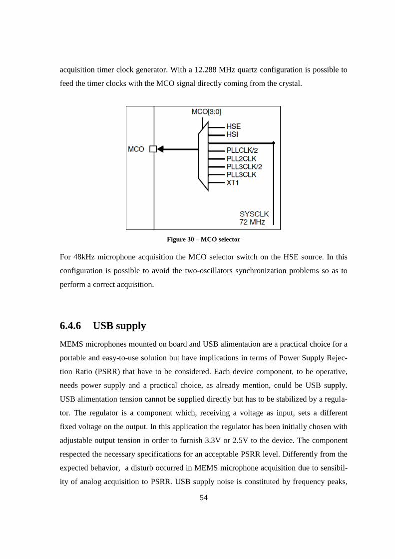
54
acquisition timer clock generator. With a 12.288 MHz quartz configuration is possible to
feed the timer clocks with the MCO signal directly coming from the crystal.
Figure 30 – MCO selector
For 48kHz microphone acquisition the MCO selector switch on the HSE source. In this
configuration is possible to avoid the two-oscillators synchronization problems so as to
perform a correct acquisition.
6.4.6 USB supply
MEMS microphones mounted on board and USB alimentation are a practical choice for a
portable and easy-to-use solution but have implications in terms of Power Supply Rejec-
tion Ratio (PSRR) that have to be considered. Each device component, to be operative,
needs power supply and a practical choice, as already mention, could be USB supply.
USB alimentation tension cannot be supplied directly but has to be stabilized by a regula-
tor. The regulator is a component which, receiving a voltage as input, sets a different
fixed voltage on the output. In this application the regulator has been initially chosen with
adjustable output tension in order to furnish 3.3V or 2.5V to the device. The component
respected the necessary specifications for an acceptable PSRR level. Differently from the
expected behavior, a disturb occurred in MEMS microphone acquisition due to sensibil-
ity of analog acquisition to PSRR. USB supply noise is constituted by frequency peaks,
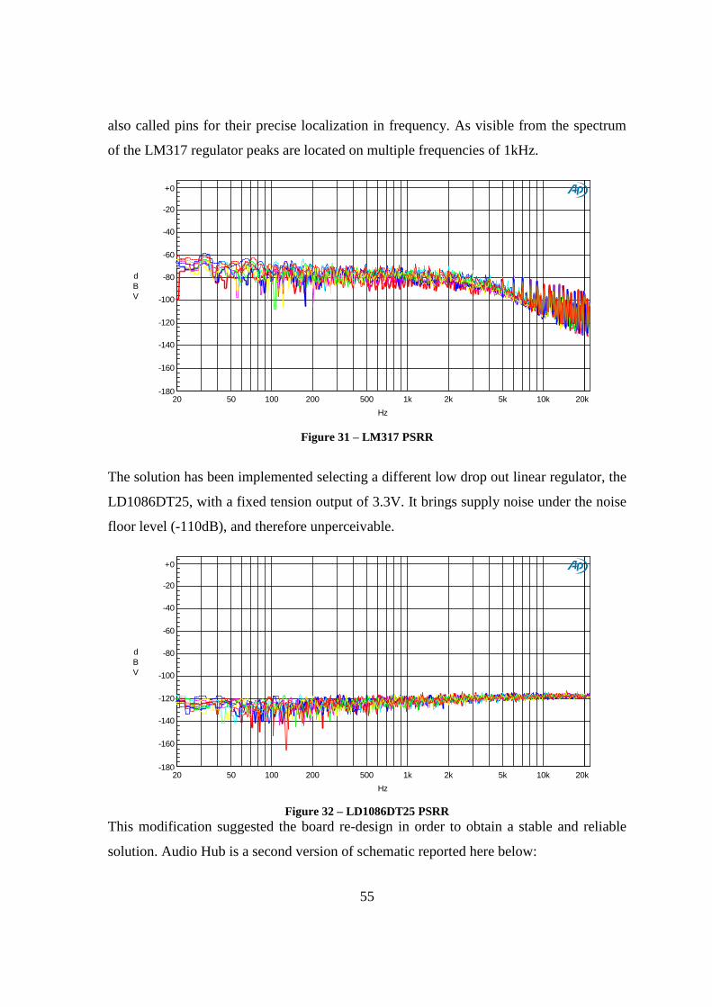
55
also called pins for their precise localization in frequency. As visible from the spectrum
of the LM317 regulator peaks are located on multiple frequencies of 1kHz.
ColorSweep Trace Line Style Thick Data Axis Comment
1 1 Red Solid 2 Fft.Ch.1 Ampl Left
2 1 Blue Solid 2 Fft.Ch.1 Ampl Left
3 1 Yellow Solid 1 Fft.Ch.1 Ampl Left
4 1 Red Solid 1 Fft.Ch.1 Ampl Left
5 1 Magenta Solid 1 Fft.Ch.1 Ampl Left
6 1 Blue Solid 1 Fft.Ch.1 Ampl Left
7 1 Cyan Solid 1 Fft.Ch.1 Ampl Left
-180
+0
-160
-140
-120
-100
-80
-60
-40
-20
d
B
V
20 20k50 100 200 500 1k 2k 5k 10k
Hz
Figure 31 – LM317 PSRR
The solution has been implemented selecting a different low drop out linear regulator, the
LD1086DT25, with a fixed tension output of 3.3V. It brings supply noise under the noise
floor level (-110dB), and therefore unperceivable.
ColorSweep Trace Line Style Thick Data Axis Comment
1 1 Red Solid 2 Fft.Ch.1 Ampl Left
2 1 Blue Solid 2 Fft.Ch.1 Ampl Left
3 1 Yellow Solid 1 Fft.Ch.1 Ampl Left
4 1 Red Solid 1 Fft.Ch.1 Ampl Left
5 1 Magenta Solid 1 Fft.Ch.1 Ampl Left
6 1 Blue Solid 1 Fft.Ch.1 Ampl Left
7 1 Cyan Solid 1 Fft.Ch.1 Ampl Left
-180
+0
-160
-140
-120
-100
-80
-60
-40
-20
d
B
V
20 20k50 100 200 500 1k 2k 5k 10k
Hz
Figure 32 – LD1086DT25 PSRR
This modification suggested the board re-design in order to obtain a stable and reliable
solution. Audio Hub is a second version of schematic reported here below:
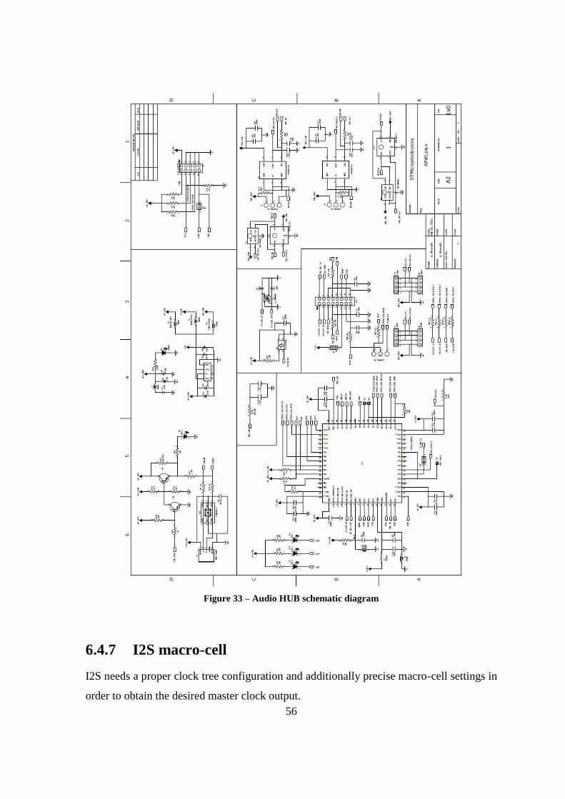
56
Figure 33 – Audio HUB schematic diagram
6.4.7 I2S macro-cell
I2S needs a proper clock tree configuration and additionally precise macro-cell settings in
order to obtain the desired master clock output.

57
Figure 34 – STM32 I2S Macro-cell
ST Standard Libraries for I2S allows a high-level configuration for macro-cell initializa-
tion. Basically is not possible to modify parameters in order to reach every possible set-
ting. The function implemented for this behaviour is:
I2SInit(SPIx,&I2SInitStructure);
This configuration limit was sufficient for the solution with 14.7456MHz crystal (see
chapter audio configuration clock tree) but adaptation to 12.288 MHz quartz bring to the
necessity of a lower level of detail. The function implemented for this usage it is been the
following:
I2SInitExt(SPIx,&InitStructure,ExtClock);
The added input parameter represents the effectively clock which will be divided by the
I2S macro-cell and used for audio streaming. Inside the function is possible to define the
divisor and add bits (I2SDIV and I2SODD) for all possible configurations according to
this equation:
Where Fs is the sampling frequency, I2SxClk is the I2S input-clock and Dbit is the data
bits.

58
6.4.8 DFU/Application subdivision
The DFU implementation has been organized in an actual split of the firmware frame-
work. In fact the code has been divided in two IAR project: one dedicated to DFU and the
other for the application and future upgrades. This choice has been related to the fact that
the DFU, to be adoptable, has to define different flash memory zones for each of the two
configurations. In case of upgrade the previous application has to be overwritten while the
DFU side has to remain unmodified. If a single project has to be implemented each DFU-
related file should be placed in the initial zone of memory and the others in a sufficient
distant area. The registers of flash memory are placed from the address 0x08000000 to
the address 0x0803FFFF as visible from the memory location map:
Figure 35 – Memory location map
With the project split the subdivision becomes practical thanks to a modifiable start ad-
dress. The DFU project has been leaved at the preset start address register configuration
while the application start register, as all the other successive upgradable versions, has
been moved with a fixed offset of 0x00008000. The offset regards the internal project
flash base address define and other defines related to actual flash memory usage, such as
the Eeprom Emulation. Also the external project file stm32f10x_flash.icf has to be modi-
fied in order to obtain the actual register offset.
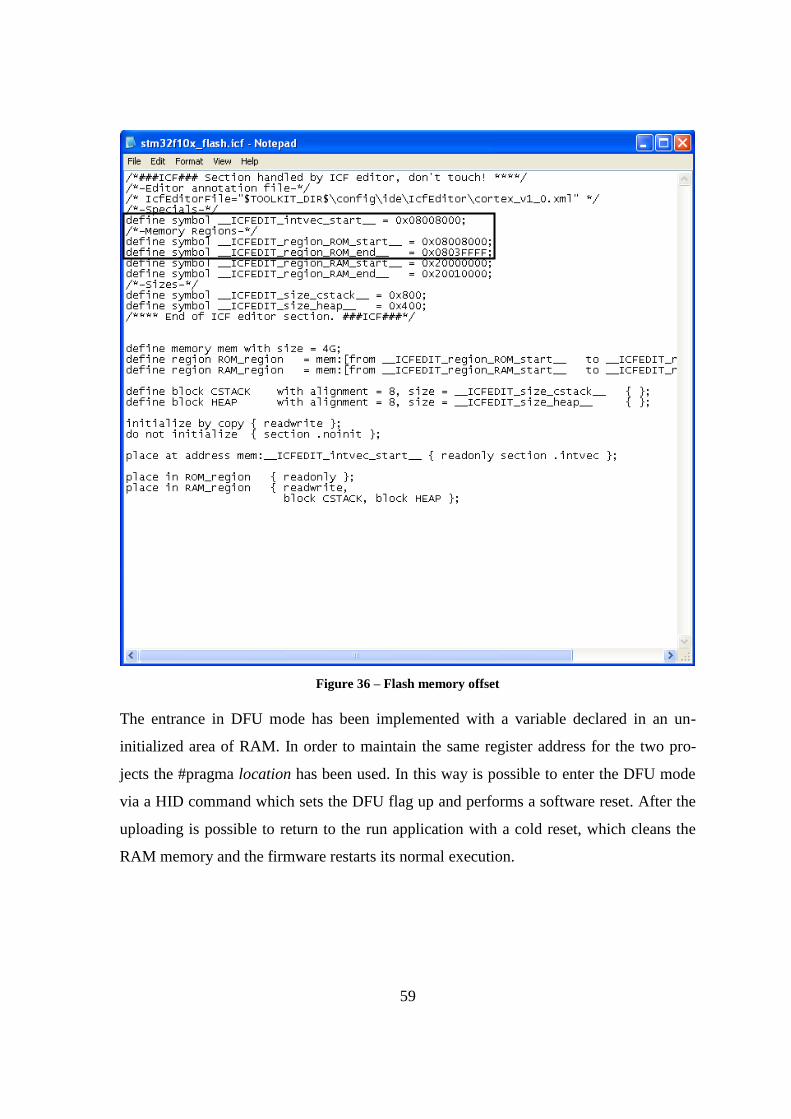
59
Figure 36 – Flash memory offset
The entrance in DFU mode has been implemented with a variable declared in an un-
initialized area of RAM. In order to maintain the same register address for the two pro-
jects the #pragma location has been used. In this way is possible to enter the DFU mode
via a HID command which sets the DFU flag up and performs a software reset. After the
uploading is possible to return to the run application with a cold reset, which cleans the
RAM memory and the firmware restarts its normal execution.

60
6.5 Software Development
This phase has been hardly connected to the device test. Software is the main core of the
framework and it has represented also a useful tool for testing firmware capabilities. In
fact firmware implementation including a USB stream does not permit debug run mode. It
limits step-by-step tracing and problem solving of not-syntax errors. Host controls each
firmware implementation phase and after HID bridge has been completed also a numeric
feedback of execution becomes available, feasible for self-made debugging.
The tool chosen for software development has been Microsoft Visual Studio. The prefer-
ence has been dictated due to facilities in graphical interfaces programming, language
similarities with the firmware development environment. In fact the language has been
C++ which is basically an extension of its predecessor which introduces class utilization.
Another influence factor has been related to the final host-side target which is based on
already existing tool: the Audio P Workbench also known as APWorkbench. As already
introduced in Software Design paragraph the actual implementation regards three differ-
ent software tools for HID communication, Audio evaluation and DFU management.
6.5.1 HID communication
As planned in design stage, the HID tool has been organized in a three layers structure.
Implementation started from a rude interface constituted by two hexadecimal tables
whose allow to operatively check the USB-side APIs for send and receive HID reports.
So initially just the lower level functioning has been tested.

61
Figure 37 – HID software interface
After this phase has been consolidated, development moved to higher level functionalities
such as I2C write, read and successively multi-write and multi-read. The screenshot be-
low shows functionalities implemented. These are not only related to the I2C communica-
tion bridge. The panel on the right regards firmware configurations and is subdivided in:
EEprom emulation configurations, whose are stored in a portion of the embedded flash
and recalled after a reset command, and Dynamic configurations, whose change configu-
ration in the actual on-going application.

62
Figure 38 – HID APWLnk+ testing Framework
Also a custom function derived from the single I2C write has been implemented: the mul-
ti-single-write. It has been developed to reduce performance gap between FTDI, the pre-
vious technology implemented for dynamic host-based I2C communication, and HID.
Multi-single-write acts as a multi-write but without constraints regarding addresses con-
sequentiality. It is possible to define a series of couples address-data up to the maximum
size of single HID transfer (64 byte). With this method the time direction limit is balanced
by a space direction optimization. This implementation is necessary particularly in initial-
ization phase, when the software sets all the DUT registers and coefficients, if configura-
ble, at default value. Successively the parser has been defined and implemented with a lit-
tle interface for boot capabilities. This functionality allows saving a booting configuration
from host directly to the init-structure stored in an un-initialized portion of RAM. After a
reset command, performed by software, the configuration is effectively ran by the
STM32.The successive implemented feature has been related to system commands. Each
DUT has standard communication lines for its monitoring and to handle critical phases.
Such lines presented on device schematic are: reset, standby, fail, master clock and mute.

63
Chapter 7
Tool Test
The following chapter deals with device test as another stage of the design flow. That is
because, as pointed out before, the design flow stages are evidently related to this phase.
In fact after a small step in the development then was implemented a local test to ensure a
behaviour in line with the requirements. These tests are mainly structured in quality tests
for audio stream and robustness/performance tests for HID channel.
7.1 PDM
To evaluate a microphone acquisition is not possible to choice a pure test-signal. Envi-
ronmental noise is always present and the source signal is normally exposed to non-
linearity. It is also true that digital microphone artefacts deeply differ from on-source
noise and, if observed carefully, the two can be discerned with drawbacks in terms of
time loss. For this reason the Acoustic Coupler tool has been adopted. It helps to feed the
source with an assessable signal minimizing its degrees of freedom. This instrument is an
64
anechoic pipette connector with a mini-jack output. It allows to choice a meaningful sig-
nal test which can be confronted to the recorded one.
PDM acquisition testing has been performed with this host-device solution: Acoustic
Coupler is connected to host analog headphones output and a generated sinusoid is
played. The STM32 configured in capture mode acquires the played signal from the
acoustic coupled microphones and directly streams data to USB. A bit-to-bit confronta-
tion is not realizable due to the analog stage so it is performed a waveform visual check in
order to evidence possible artefact occurrences. Example figures better explain the meth-
odologies and show the error typologies.
7.2 I2S stream
A digital I2S audio stream, as seen in the protocol chapter, is basically a three lines sig-
nal. In order to evaluate its coherency with respect to the protocol is sufficient to perform
a control based on its digital behavior. Using an oscilloscope is possible to evaluate signal
integrity highlighting eventually occurred errors. I2S protocol, differently from other
standards such as USB, is made by visual characteristics. WS clock has a periodicity
which reveals the actual I2S frequency of acquisition.

65
Figure 39 – 16-bit SDA, WS 48kHz and SCK
I2S data line is characterized by a single step bit before the actual data and the possibility,
using the bit clock, of number of data bits verification for each word selected frame.
Figure 40 – I2S SCK bit-clock
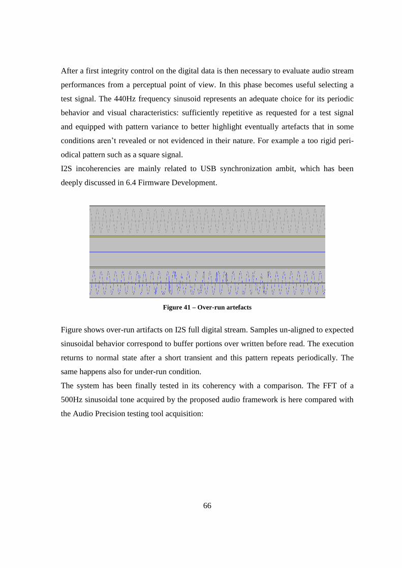
66
After a first integrity control on the digital data is then necessary to evaluate audio stream
performances from a perceptual point of view. In this phase becomes useful selecting a
test signal. The 440Hz frequency sinusoid represents an adequate choice for its periodic
behavior and visual characteristics: sufficiently repetitive as requested for a test signal
and equipped with pattern variance to better highlight eventually artefacts that in some
conditions aren’t revealed or not evidenced in their nature. For example a too rigid peri-
odical pattern such as a square signal.
I2S incoherencies are mainly related to USB synchronization ambit, which has been
deeply discussed in 6.4 Firmware Development.
Figure 41 – Over-run artefacts
Figure shows over-run artifacts on I2S full digital stream. Samples un-aligned to expected
sinusoidal behavior correspond to buffer portions over written before read. The execution
returns to normal state after a short transient and this pattern repeats periodically. The
same happens also for under-run condition.
The system has been finally tested in its coherency with a comparison. The FFT of a
500Hz sinusoidal tone acquired by the proposed audio framework is here compared with
the Audio Precision testing tool acquisition:
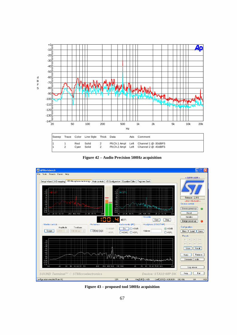
67
Audio Precision 11/26/12 17:57:19
coupon test.at2c
ColorSweep Trace Line Style Thick Data Axis Comment
1 1 Red Solid 2 Fft.Ch.1 Ampl Left Channel 1 @ -30dBFS
1 2 Cyan Solid 2 Fft.Ch.2 Ampl Left Channel 2 @ -40dBFS
-140
+0
-130
-120
-110
-100
-90
-80
-70
-60
-50
-40
-30
-20
-10
d
B
F
S
20 20k50 100 200 500 1k 2k 5k 10k
Hz
Figure 42 – Audio Precision 500Hz acquisition
Figure 43 – proposed tool 500Hz acquisition
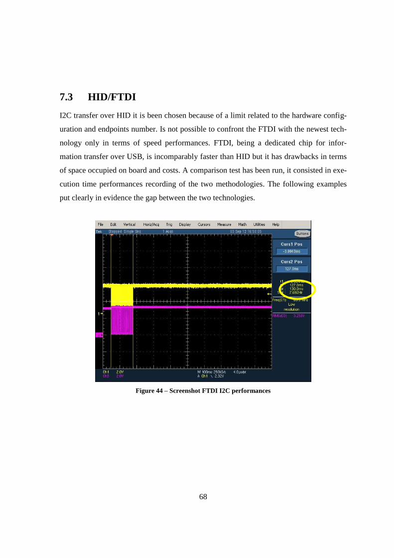
68
7.3 HID/FTDI
I2C transfer over HID it is been chosen because of a limit related to the hardware config-
uration and endpoints number. Is not possible to confront the FTDI with the newest tech-
nology only in terms of speed performances. FTDI, being a dedicated chip for infor-
mation transfer over USB, is incomparably faster than HID but it has drawbacks in terms
of space occupied on board and costs. A comparison test has been run, it consisted in exe-
cution time performances recording of the two methodologies. The following examples
put clearly in evidence the gap between the two technologies.
Figure 44 – Screenshot FTDI I2C performances
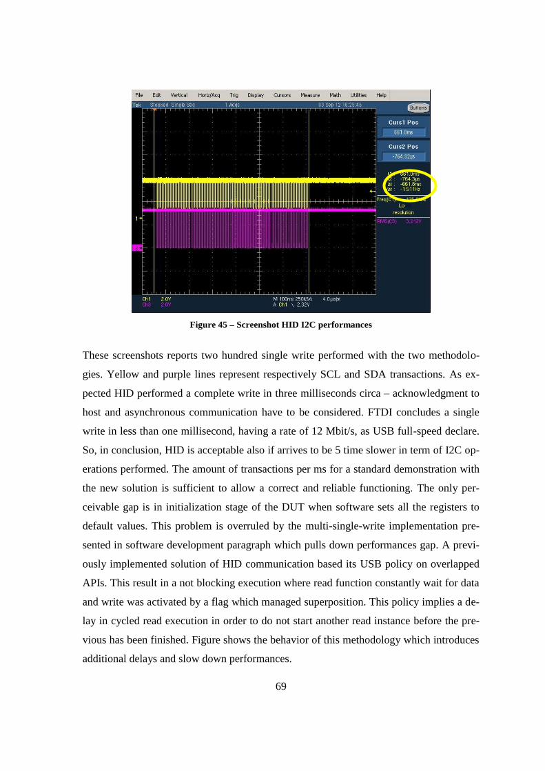
69
Figure 45 – Screenshot HID I2C performances
These screenshots reports two hundred single write performed with the two methodolo-
gies. Yellow and purple lines represent respectively SCL and SDA transactions. As ex-
pected HID performed a complete write in three milliseconds circa – acknowledgment to
host and asynchronous communication have to be considered. FTDI concludes a single
write in less than one millisecond, having a rate of 12 Mbit/s, as USB full-speed declare.
So, in conclusion, HID is acceptable also if arrives to be 5 time slower in term of I2C op-
erations performed. The amount of transactions per ms for a standard demonstration with
the new solution is sufficient to allow a correct and reliable functioning. The only per-
ceivable gap is in initialization stage of the DUT when software sets all the registers to
default values. This problem is overruled by the multi-single-write implementation pre-
sented in software development paragraph which pulls down performances gap. A previ-
ously implemented solution of HID communication based its USB policy on overlapped
APIs. This result in a not blocking execution where read function constantly wait for data
and write was activated by a flag which managed superposition. This policy implies a de-
lay in cycled read execution in order to do not start another read instance before the pre-
vious has been finished. Figure shows the behavior of this methodology which introduces
additional delays and slow down performances.
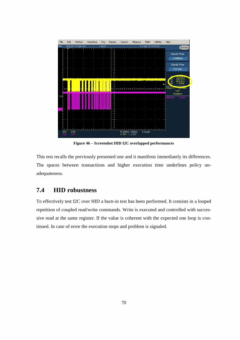
70
Figure 46 – Screenshot HID I2C overlapped performances
This test recalls the previously presented one and it manifests immediately its differences.
The spaces between transactions and higher execution time underlines policy un-
adequateness.
7.4 HID robustness
To effectively test I2C over HID a burn-in test has been performed. It consists in a looped
repetition of coupled read/write commands. Write is executed and controlled with succes-
sive read at the same register. If the value is coherent with the expected one loop is con-
tinued. In case of error the execution stops and problem is signaled.
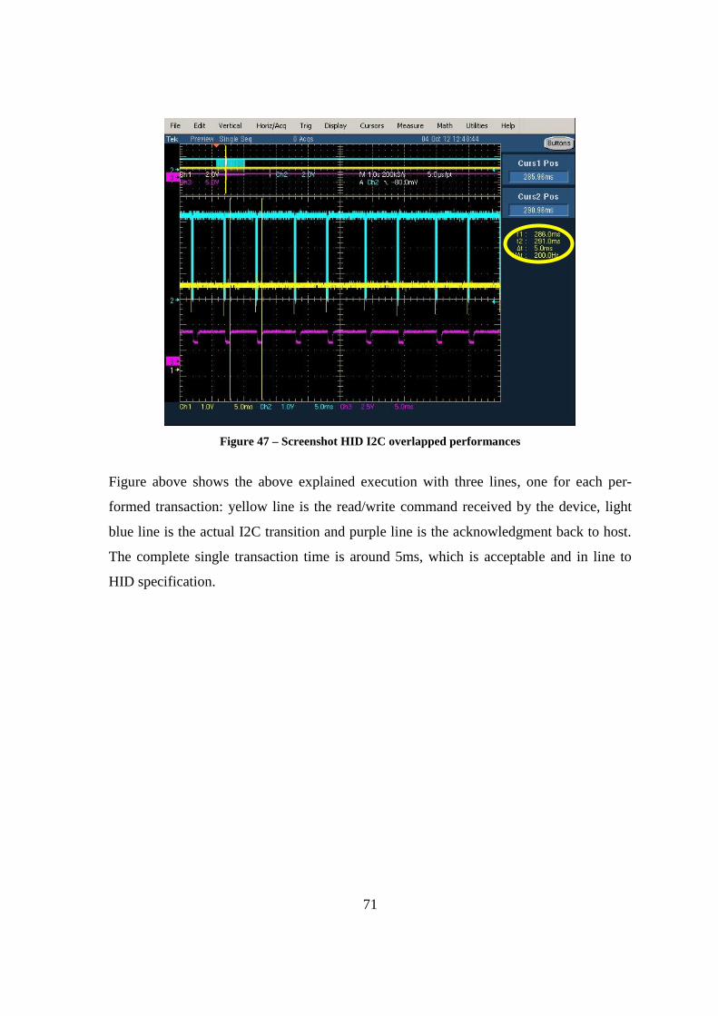
71
Figure 47 – Screenshot HID I2C overlapped performances
Figure above shows the above explained execution with three lines, one for each per-
formed transaction: yellow line is the read/write command received by the device, light
blue line is the actual I2C transition and purple line is the acknowledgment back to host.
The complete single transaction time is around 5ms, which is acceptable and in line to
HID specification.
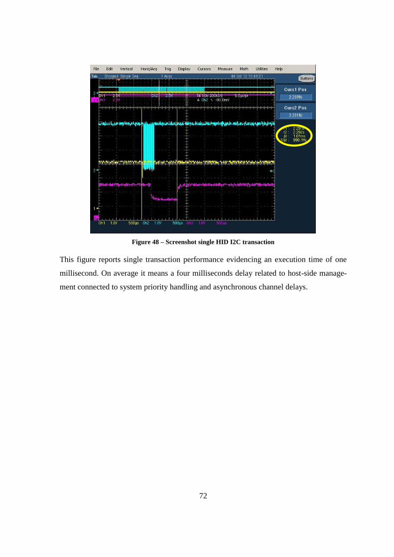
72
Figure 48 – Screenshot single HID I2C transaction
This figure reports single transaction performance evidencing an execution time of one
millisecond. On average it means a four milliseconds delay related to host-side manage-
ment connected to system priority handling and asynchronous channel delays.
73
Chapter 8
Conclusion and future work
The proposed platform reaches performances comparable to other solutions described in
literature with dimension and cost advantages. It is equipped with all the capabilities de-
fined in the Specifications and Requirements chapter. The solution is therefore a visual-
based test sufficient to obtain reliable results in digital MEMS microphones evaluation.
The entire digital audio chain has been tested with a high precision testing tool in order to
verify the data channel coherency. Its flexibility allows other usage contexts related to
audio systems, such as characterization of non-MEMS microphones, or evaluation of
sound terminals. In the chapter 2 the State of the Art of testing/evaluation tools has been
analyzed, in order to contextualize the proposed solution in its field of application. In
chapter 3 the environment chosen for the development of the audio framework has been
described. Chapter 4 has been an excursus on the technologies adopted for the proposed
solution. These are optimized for the audio digital stream from the device to the host. In
chapter 5 the Specifications & Requirements defined from the analysis about the state of
the art have been listed. Chapter 6 has focused on the Implementation, facing the practical
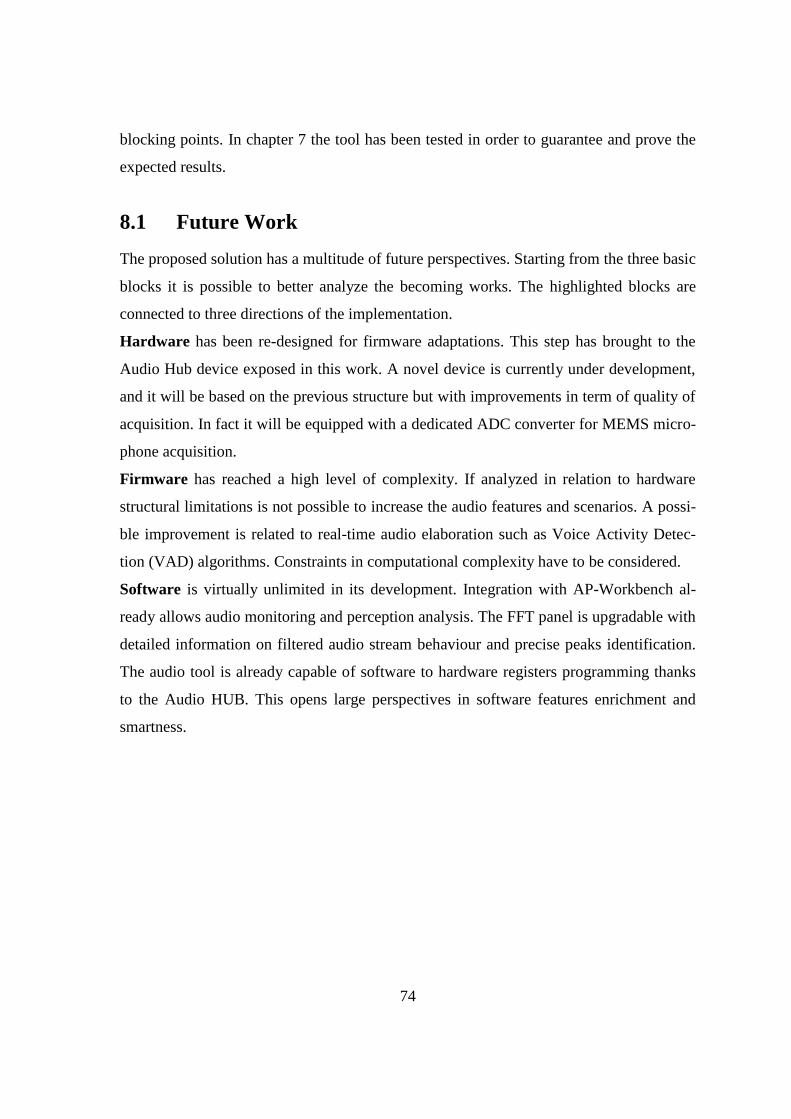
74
blocking points. In chapter 7 the tool has been tested in order to guarantee and prove the
expected results.
8.1 Future Work
The proposed solution has a multitude of future perspectives. Starting from the three basic
blocks it is possible to better analyze the becoming works. The highlighted blocks are
connected to three directions of the implementation.
Hardware has been re-designed for firmware adaptations. This step has brought to the
Audio Hub device exposed in this work. A novel device is currently under development,
and it will be based on the previous structure but with improvements in term of quality of
acquisition. In fact it will be equipped with a dedicated ADC converter for MEMS micro-
phone acquisition.
Firmware has reached a high level of complexity. If analyzed in relation to hardware
structural limitations is not possible to increase the audio features and scenarios. A possi-
ble improvement is related to real-time audio elaboration such as Voice Activity Detec-
tion (VAD) algorithms. Constraints in computational complexity have to be considered.
Software is virtually unlimited in its development. Integration with AP-Workbench al-
ready allows audio monitoring and perception analysis. The FFT panel is upgradable with
detailed information on filtered audio stream behaviour and precise peaks identification.
The audio tool is already capable of software to hardware registers programming thanks
to the Audio HUB. This opens large perspectives in software features enrichment and
smartness.
Appendix
MEMS Microphone - MP34DT01
The MP34DT01 is an ultra-compact, low-power, omnidirectional, digital MEMS
microphone built with a capacitive sensing element and an IC interface. The sens-
ing element, capable of detecting acoustic waves, is manufactured using a special-
ized silicon micromachining process dedicated to produce audio sensors.
Figure 49 – MEMS Microphone - MP34DT01
The IC interface is manufactured using a CMOS process that allows designing a
dedicated circuit able to provide a digital signal externally in PDM format.
The MP34DT01 has an acoustic overload point of 120 dBSPL with a 63 dB sig-
nal-to-noise ratio and –26 dBFS sensitivity. The MP34DT01 is available in a top-
port, SMD compliant, EMI-shielded package and is guaranteed to operate over an
extended temperature range from -40 °C to +85 °C.
APWorkbench
The Audio Processor Workbench is a software tool of ST Microelectronics. It per-
forms elaboration and audio processing. It is actually compatible with any device
to host audio streaming but the features combined with the hardware link (AP-
WLink – APWLink+) enables an higher level of DUT configurability. In fact with
the I2C communication protocol allows a configuration personalization related to
the device features. It can be, for example, a software handler for sound terminal
initialization.
APWLink
The APWLink is the first bridge device associated to the APWorkbench. It has
been created mainly for ST Sound Terminals family. It is equipped with audio
protocol for input/output. It does not actually generate itself an audio stream but
acts as a bridge. The formats available are: I2S to I2S, Analog to I2S, SPDIF to
I2S. A Full Speed dedicated USB channel for I2C from host via FTDI is used for
a combined usage with the APWorkbench suite allowing a high level interface for
register configurations.
APWLink+
APWlink+ hosts the microcontroller STM32F107RC and either the MP45DT02
or MP34DT01 (top-port digital microphones) and the MP34DB01 (bottom-port
digital microphone). Microphones are analog-to-digital transducers, in other
words, they are able to sense sound pressure and convert this signal to a digital
signal using the PDM technique. The STM32 microcontroller decodes the PDM
signal coming from the microphones and streams the audio via the USB. This
document will provide a brief description of the software that decodes the PDM
signal and also information about the hardware as well as simple steps to use the
board.
STA326/8/9
The STA326 comprises digital audio processing, digital amplifier control and
DDX® power output stage to create a high-power single-chip DDX® solution for
high-quality, high-efficiency, all-digital amplification. The STA326 power section
consists of four independent half-bridges. These can be configured via digital con-
trol to operate in different modes. 2.1 channels can be provided by two half-
bridges and a single full-bridge to give up to 2 x 40 W plus 1 x 80 W of power
output. Two channels can be provided by two full-bridges to give up to 2 x 80 W
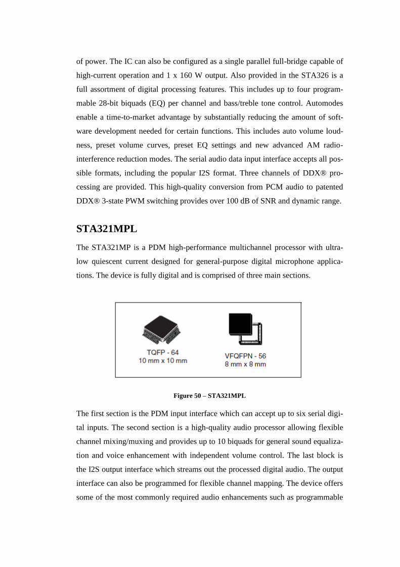
of power. The IC can also be configured as a single parallel full-bridge capable of
high-current operation and 1 x 160 W output. Also provided in the STA326 is a
full assortment of digital processing features. This includes up to four program-
mable 28-bit biquads (EQ) per channel and bass/treble tone control. Automodes
enable a time-to-market advantage by substantially reducing the amount of soft-
ware development needed for certain functions. This includes auto volume loud-
ness, preset volume curves, preset EQ settings and new advanced AM radio-
interference reduction modes. The serial audio data input interface accepts all pos-
sible formats, including the popular I2S format. Three channels of DDX® pro-
cessing are provided. This high-quality conversion from PCM audio to patented
DDX® 3-state PWM switching provides over 100 dB of SNR and dynamic range.
STA321MPL
The STA321MP is a PDM high-performance multichannel processor with ultra-
low quiescent current designed for general-purpose digital microphone applica-
tions. The device is fully digital and is comprised of three main sections.
Figure 50 – STA321MPL
The first section is the PDM input interface which can accept up to six serial digi-
tal inputs. The second section is a high-quality audio processor allowing flexible
channel mixing/muxing and provides up to 10 biquads for general sound equaliza-
tion and voice enhancement with independent volume control. The last block is
the I2S output interface which streams out the processed digital audio. The output
interface can also be programmed for flexible channel mapping. The device offers
some of the most commonly required audio enhancements such as programmable
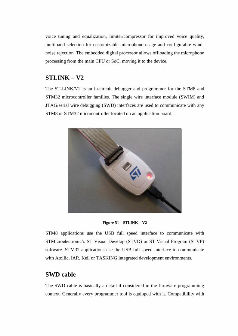
voice tuning and equalization, limiter/compressor for improved voice quality,
multiband selection for customizable microphone usage and configurable wind-
noise rejection. The embedded digital processor allows offloading the microphone
processing from the main CPU or SoC, moving it to the device.
STLINK – V2
The ST-LINK/V2 is an in-circuit debugger and programmer for the STM8 and
STM32 microcontroller families. The single wire interface module (SWIM) and
JTAG/serial wire debugging (SWD) interfaces are used to communicate with any
STM8 or STM32 microcontroller located on an application board.
Figure 51 – STLINK – V2
STM8 applications use the USB full speed interface to communicate with
STMicroelectronic’s ST Visual Develop (STVD) or ST Visual Program (STVP)
software. STM32 applications use the USB full speed interface to communicate
with Atollic, IAR, Keil or TASKING integrated development environments.
SWD cable
The SWD cable is basically a detail if considered in the firmware programming
context. Generally every programmer tool is equipped with it. Compatibility with
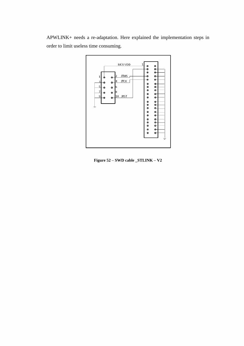
APWLINK+ needs a re-adaptation. Here explained the implementation steps in
order to limit useless time consuming.
Figure 52 – SWD cable _STLINK – V2
Bibliography
[1]. Philips Semiconductor. I2C specification, 1995.
[2]. Philips Semiconductor, I2S specification, 1996
[3]. ST, STM32F105xx/107xx Datasheet, 2011
[4]. ST, Reference Manual STM32F10xxx advanced ARM-based 32-bit MCUs,
2011
[5]. Shyam Sadasivan. Introduction to the ARM Cortex-M3 Processor, 2006.
[6]. ARM, Cortex™-M3 Devices, 2010
[7]. Ronald E. Crochiere, Interpolation and Decimation of Digital Signals, 1981
[8]. Intel Corporation, Universal Serial Bus Common Class Specification, 1997
[9]. USB, Universal Serial Bus Specification, 2007
[10]. USB IF, Universal Serial Device Class Definition for Audio Data Formats,
1998
[11]. ST, MP34DT01 MEMS audio sensor omnidirectional digital microphone,
July 2012
[12]. ST, AN4146 STSmartVoice demonstration board STEVAL - MKI126Vx
October 2012
[13]. Maxim, MAX98089 Evaluation Kit Available 2011
[14]. Silicon Labs, CP2114 Single-chip USB Audio to I2S Digital Bridge, 2012
[15]. Analog Devices, EVAL - ADMP441 I2S MEMS Microphone, 2012
[16]. Audio Precision, PDM option for APx, 2012
[17]. ST, AN4118 APWLink USB interface board
[18]. ST, AN3998 PDM audio software decoding on STM32 microcontrollers,
October 2011
[19]. USB, Interface Association Descriptors, 2012
[20]. ST, STM32F10xxx Flash memory microcontrollers, August 2012
[21]. ST, AN2824 STM32F10xxx I2C optimized examples, June 2010
[22]. ST, STA321MP Scalable digital microphone processor, February 2012
[23]. USB, USB Interface Association Descriptor Device Class Code and Use
Model, July 2003