polyethylene glycol diacrylate (pegda) resin development
TRANSCRIPT

Brigham Young University Brigham Young University
BYU ScholarsArchive BYU ScholarsArchive
Theses and Dissertations
2015-05-01
Polyethylene Glycol Diacrylate (PEGDA) Resin Development for Polyethylene Glycol Diacrylate (PEGDA) Resin Development for
3D-Printed Microfluidic Devices 3D-Printed Microfluidic Devices
Kamran Qaderi Brigham Young University - Provo
Follow this and additional works at: https://scholarsarchive.byu.edu/etd
Part of the Electrical and Computer Engineering Commons
BYU ScholarsArchive Citation BYU ScholarsArchive Citation Qaderi, Kamran, "Polyethylene Glycol Diacrylate (PEGDA) Resin Development for 3D-Printed Microfluidic Devices" (2015). Theses and Dissertations. 5555. https://scholarsarchive.byu.edu/etd/5555
This Thesis is brought to you for free and open access by BYU ScholarsArchive. It has been accepted for inclusion in Theses and Dissertations by an authorized administrator of BYU ScholarsArchive. For more information, please contact [email protected], [email protected].

Polyethylene Glycol Diacrylate (PEGDA) Resin Development for 3D-Printed Microfluidic
Devices
Kamran Qaderi
A thesis submitted to the faculty ofBrigham Young University
in partial fulfillment of the requirements for the degree of
Master of Science
Gregory P. Nordin, ChairAdam T. WoolleyBrian A. Mazzeo
Department of Electrical and Computer Engineering
Brigham Young University
May 2015
Copyright © 2015 Kamran Qaderi
All Rights Reserved

ABSTRACT
Polyethylene Glycol Diacrylate (PEGDA) Resin Development for 3D-Printed MicrofluidicDevices
Kamran QaderiDepartment of Electrical and Computer Engineering, BYU
Master of Science
In this thesis, the successful fabrication of 3D-printed microfluidic devices will be dis-cussed. Fabrication is performed with a low-cost commercially available stereolithographic 3Dprinter utilizing a custom PEGDA resin formulation tailored for low non-specific protein adsorp-tion based on my colleagues’ work [Rogers et al., Anal. Chem. 83, 6418 (2011)]. Horizontalmicrofluidic channels with designed rectangular cross sectional dimensions as small as 300 µmwide and 150 µm tall are printed with 100% yield, as are cylindrical vertical microfluidic channelswith 300 µm designed (334 µm actual) diameters. Moreover, two different resins developed byour group are utilized in the process of 3D-printing which is the novel aspect about this thesis sinceother groups have not done research on this aspect of 3D-printing.
Keywords: Microfluidics, polyethylene glycol diacrylate (PEGDA), stereolithography, 3D-printing

ACKNOWLEDGMENTS
Foremost, I would like to express my sincere gratitude to my advisor Prof. Greg Nordin
for the continuous support of my study and research, for his patience, motivation, enthusiasm, and
immense knowledge. His guidance helped me in all the time of research and writing of this thesis.
Besides my advisor, I would like to thank the rest of my thesis committee: Prof. Adam
Woolley and Prof. Brian Mazzeo.
I thank my fellow labmates: Ben Tsai, Dr. Chad Rogers, Gong Hua, Mike Beauchamp,
Katie Jones, and Steven Perry for the stimulating discussions, and for all the fun we have had in
the last two years. I also thank my friend Rashid Mehmood for his helpful ideas and comments
during these two years and my Iranian friends as well.
Last but not the least, I would like to thank my parents, for giving birth to me in the first
place and supporting me spiritually throughout my life. I owe my deepest thanks to my lovely
fiancee, Shiva, who has cheered me through the good times and especially the bad. She has been
the source of energy during the dull moments and shown remarkable patience with me.
TABLE OF CONTENTS
LIST OF TABLES . . . . . . . . . . . . . . . . . . . . . . . . . . . . . . . . . . . . . . . vi
LIST OF FIGURES . . . . . . . . . . . . . . . . . . . . . . . . . . . . . . . . . . . . . . vii
Chapter 1 Introduction . . . . . . . . . . . . . . . . . . . . . . . . . . . . . . . . . . . 1
Chapter 2 Background . . . . . . . . . . . . . . . . . . . . . . . . . . . . . . . . . . . 3
2.1 Microfluidics in General . . . . . . . . . . . . . . . . . . . . . . . . . . . . . . . 3
2.1.1 Why Microfluidics? . . . . . . . . . . . . . . . . . . . . . . . . . . . . . 3
2.1.2 Applications of Microfluidics . . . . . . . . . . . . . . . . . . . . . . . . 3
2.1.3 Internal Microfluidic Elements . . . . . . . . . . . . . . . . . . . . . . . . 5
2.1.4 Fabrication Methods of Microfluidic Devices . . . . . . . . . . . . . . . . 6
2.1.5 Rapid Prototyping . . . . . . . . . . . . . . . . . . . . . . . . . . . . . . 7
2.2 3D-Printing for Microfluidics . . . . . . . . . . . . . . . . . . . . . . . . . . . . . 9
2.2.1 Different 3D-Printers, Price and Resolution (X-Y/Z) . . . . . . . . . . . . 11
2.3 Resin Formulation . . . . . . . . . . . . . . . . . . . . . . . . . . . . . . . . . . 12
2.3.1 Monomer . . . . . . . . . . . . . . . . . . . . . . . . . . . . . . . . . . . 12
2.3.2 Photoinitiator (PI) . . . . . . . . . . . . . . . . . . . . . . . . . . . . . . 13
2.3.3 Absorber . . . . . . . . . . . . . . . . . . . . . . . . . . . . . . . . . . . 15
Chapter 3 Asiga 3D-Printer . . . . . . . . . . . . . . . . . . . . . . . . . . . . . . . . 16
3.1 Asiga Pico27 3D-Printer . . . . . . . . . . . . . . . . . . . . . . . . . . . . . . . 16
3.1.1 Calibration . . . . . . . . . . . . . . . . . . . . . . . . . . . . . . . . . . 16
3.1.2 Operation of Printer . . . . . . . . . . . . . . . . . . . . . . . . . . . . . 16
3.2 Die Design . . . . . . . . . . . . . . . . . . . . . . . . . . . . . . . . . . . . . . 17
3.3 Die Fabrication . . . . . . . . . . . . . . . . . . . . . . . . . . . . . . . . . . . . 18
iv

Chapter 4 Resin Formulation I . . . . . . . . . . . . . . . . . . . . . . . . . . . . . . 21
4.1 Chemicals Present in the Resin Formulation . . . . . . . . . . . . . . . . . . . . . 21
4.1.1 Monomer . . . . . . . . . . . . . . . . . . . . . . . . . . . . . . . . . . . 21
4.1.2 Photoinitiator . . . . . . . . . . . . . . . . . . . . . . . . . . . . . . . . . 21
4.1.3 UV Absorber . . . . . . . . . . . . . . . . . . . . . . . . . . . . . . . . . 22
4.2 Resin Formulation . . . . . . . . . . . . . . . . . . . . . . . . . . . . . . . . . . 23
4.3 Results . . . . . . . . . . . . . . . . . . . . . . . . . . . . . . . . . . . . . . . . . 24
4.4 Discussion . . . . . . . . . . . . . . . . . . . . . . . . . . . . . . . . . . . . . . . 27
Chapter 5 Resin Formulation II . . . . . . . . . . . . . . . . . . . . . . . . . . . . . . 31
5.1 Materials . . . . . . . . . . . . . . . . . . . . . . . . . . . . . . . . . . . . . . . 31
5.1.1 Photoinitiator . . . . . . . . . . . . . . . . . . . . . . . . . . . . . . . . . 31
5.1.2 UV Absorber . . . . . . . . . . . . . . . . . . . . . . . . . . . . . . . . . 31
5.2 Quantitative Analysis of Polymerization Depth as a Function of Layer Exposure
Time . . . . . . . . . . . . . . . . . . . . . . . . . . . . . . . . . . . . . . . . . . 32
5.2.1 Definitions . . . . . . . . . . . . . . . . . . . . . . . . . . . . . . . . . . 32
5.2.2 Relationship Between Depth and Exposure Time for a Given Critical Dose 33
5.3 Results from Experiments . . . . . . . . . . . . . . . . . . . . . . . . . . . . . . . 36
5.4 Discussion . . . . . . . . . . . . . . . . . . . . . . . . . . . . . . . . . . . . . . . 37
Chapter 6 Conclusions and Future Work . . . . . . . . . . . . . . . . . . . . . . . . . 39
6.1 Conclusions . . . . . . . . . . . . . . . . . . . . . . . . . . . . . . . . . . . . . . 39
6.2 Future Work . . . . . . . . . . . . . . . . . . . . . . . . . . . . . . . . . . . . . . 39
REFERENCES . . . . . . . . . . . . . . . . . . . . . . . . . . . . . . . . . . . . . . . . . 41
v
LIST OF TABLES
2.1 Potential Applications of Microfluidic Devices. . . . . . . . . . . . . . . . . . . . 4
2.2 Comparison of Desktop Stereolithography Systems. . . . . . . . . . . . . . . . . . 12
2.3 Important Terminology for Photoinitiators. . . . . . . . . . . . . . . . . . . . . . . 14
4.1 Different Solution Concentrations. . . . . . . . . . . . . . . . . . . . . . . . . . . 24
vi

LIST OF FIGURES
2.1 Microfluidic Devices. . . . . . . . . . . . . . . . . . . . . . . . . . . . . . . . . . 5
2.2 General Process of Soft Lithography. . . . . . . . . . . . . . . . . . . . . . . . . . 6
2.3 Major Process Steps of Microinjection Molding . . . . . . . . . . . . . . . . . . . 8
2.4 Principles of Stereolithographic 3D-Printing . . . . . . . . . . . . . . . . . . . . . 10
2.5 Comparison Between (a) PDMS/Plastic Molding and (b) Stereolithography Show-
ing the Path to Commercialization. . . . . . . . . . . . . . . . . . . . . . . . . . . 11
2.6 Molecular Structure of PEGDA . . . . . . . . . . . . . . . . . . . . . . . . . . . . 13
3.1 Valve Schematic. . . . . . . . . . . . . . . . . . . . . . . . . . . . . . . . . . . . 18
3.2 Complete Design and Device Image. . . . . . . . . . . . . . . . . . . . . . . . . . 19
3.3 Device Fabrication Process. . . . . . . . . . . . . . . . . . . . . . . . . . . . . . . 20
4.1 Spectrum of the UV Absorber, the PI, and the UV LED. . . . . . . . . . . . . . . . 22
4.2 PEGDA Molecular Structure . . . . . . . . . . . . . . . . . . . . . . . . . . . . . 22
4.3 TMDPO Molecular Structure . . . . . . . . . . . . . . . . . . . . . . . . . . . . . 23
4.4 BLS-99 Molecular Structure . . . . . . . . . . . . . . . . . . . . . . . . . . . . . 23
4.5 Printed Device Using 6% TMDPO and 1% BLS-99 Concentrations. . . . . . . . . 25
4.6 Printed Device Using 10% TMDPO and 1% BLS-99 Concentrations . . . . . . . . 26
4.7 Printed Device Using 8% TMDPO and 1% BLS-99 Concentrations . . . . . . . . . 27
4.8 Horizontal Channel Fabrication, Repeatability, and Yield. . . . . . . . . . . . . . . 28
4.9 Vertical Cylindrical Channel Fabrication, Repeatability, and Yield. . . . . . . . . . 29
4.10 Test Design. . . . . . . . . . . . . . . . . . . . . . . . . . . . . . . . . . . . . . . 30
5.1 Spectrum of the UV Absorber, the PI, and the UV LED. . . . . . . . . . . . . . . . 32
5.2 Normalized Irradiance as a Function of Depth. . . . . . . . . . . . . . . . . . . . . 33
5.3 Dose as a Function of Depth for Different Layer Exposure Times. . . . . . . . . . 34
5.4 Polymerization Depth as a Function of Normalized Layer Exposure Time. . . . . . 35
vii

5.5 Designed Single-Layer Membranes . . . . . . . . . . . . . . . . . . . . . . . . . 37
5.6 Successfully Printed Device with 50 µm Membrane. . . . . . . . . . . . . . . . . 38
viii

CHAPTER 1. INTRODUCTION
Microfluidic device prototyping for proof-of-concept demonstration typically utilizes hot
embossed or injection molded plastics [1] or polydimethylsiloxane (PDMS) [1, 2]. In either case,
two or more individually fabricated layers are bonded together to form a completed device. The
fabrication process typically involves cleanroom microfabrication of molds using photolithography
for one or more of the individual layers, followed by molding and release of each layer and then
careful layer alignment and bonding. This sequence of steps can usually lead to a delay of a
week or more between completing the design of a device and actually having one in hand to test,
especially taking into account the inevitable problems that crop up for various fabrication steps in
a university environment and the turn-around time to design and procure photolithographic masks.
3D printing of microfluidics offers the opportunity to shrink the time from design to first device to
an hour or less because the device is created directly in a single step with no need for layer-by-layer
fabrication and assembly as with PDMS.
This promise that 3D printed microfluidics can dramatically lower the barrier for fabricating
sophisticated microfluidic devices, is not yet been completely realized. [3] However, there are
numerous works done in this direction. For instance, Kitson et al. [4, 5] demonstrated fluidic
devices 3D printed by extruding plastic through a heated nozzle. However, this fabrication method
is inherently unable to produce feature sizes and flow channel dimensions needed for microfluidic
(as opposed to macrofluidic or millifluidic) device fabrication. For the reported devices, the flow
channels had very large cross sections (4 mm diameter).
Another group showed that flow channels with cross sectional features down to 400 µm are
possible. However, this approach is still limited to using commercially available resins, and only
passive microfluidic components have been demonstrated. [6]
Alternatively, Shallan et al. [7] reported the use of an inexpensive commercially avail-
able stereolithographic printer (MiiCraft) to fabricate microfluidic devices with flow channel cross
1
sectional dimensions <500 µm. Unfortunately, the two available resin formulations (blue and
transparent) are proprietary and supplied by the printer manufacturer. Additionally, the transpar-
ent resin exhibits only 60% transmission for a 500 µm thick layer at wavelengths <430 nm and
exhibits absorption of small hydrophobic molecules such as rhodamine 6G.
The Fang group and collaborators have built several custom stereolithographic 3D printers
that achieve submicron feature sizes for microfluidic devices and use their own resin formulations.
[8–10] The small feature sizes are realized by photoreduction of an image projected by a UV-
illuminated dynamic mask (i.e., digital light projector or liquid crystal on silicon microdisplay).
However, the required photoreduction reduces the exposed area to only a millimeter or two on a
side. To obtain reasonable part sizes (tens of millimeters in each lateral dimension), the image
must be stepped many times across each layer using precise translation stages (250 nm positional
repeatability). The end result is a complicated and expensive system that does not lend itself to
low-cost microfluidic rapid prototyping.
The successful fabrication and testing of 3D printed microfluidic devices with integrated
membrane-based valves are reported in this thesis. Fabrication is performed with a low-cost com-
mercially available stereolithographic 3D printer. Horizontal microfluidic channels with designed
rectangular cross sectional dimensions as small as 300 µm wide and 150 µm tall are printed with
100% yield, as are cylindrical vertical microfluidic channels with 300 µm designed (334 µm ac-
tual) diameters. I use two different custom resin formulation tailored for low nonspecific protein
adsorption which is the novel aspect about this thesis since other groups have not done research on
this aspect of 3D-printing.
In this thesis, first background information is discussed (Chapter 2), including microfluidcs
in general. Stereolithographic 3D printing and resin formulation for the 3D printer is also analyzed
in detail. Next, the formulation for the resin used in my work is studied in Chapters 4 and 5.
Finally, a summary of my research on stereolithographic 3D printing will be given in Chapter 6.
2
CHAPTER 2. BACKGROUND
2.1 Microfluidics in General
The capability of fabricating patterns and structures in microscale and even smaller sizes
has lead the scientists to a wide range of investigations. One of these investigations is to manipulate
the control of fluids. The created field is called microfluidics for which the word is misleading
because the microscopic amount of samples (10−6 to 10−9 liters) are handled regardless of the size
of devices. These small volume samples are handled in channels with dimensions on the order
of hundreds of microns or less. Basically microfluidics enables to control the concentration of
molecules in space and time. Scientists care about small volumes because some live samples are
so valuable and rare to work with, therefore, small amount of them is available for experiments.
2.1.1 Why Microfluidics?
The very basic capabilities of microfluidic technologies are: the ability to handle very
small volumes of samples and reagents, and having high resolution and sensitivity in carrying out
separation and detection, low cost, quick in analysis and less hazardous compared to the traditional
engineering technologies in large volume, the possibility of parallel operation, and integration of
an entire laboratory on a single chip (lab-on-a-chip). [11, 12] These are the main reasons which
make microfluidics very important and useful.
2.1.2 Applications of Microfluidics
Utilization of microfluidic devices for fluid manipulation has a number of applications,
ranging from pharmaceuticals and biomedicine (drug design, delivery and detection, diagnostic
devices) to industrial applications of rapid chemical analyses, chemical synthesis and high through-
3

Table 2.1: Potential applications of microfluidic devices.
Area ApplicationMiniaturized analytical systemsGenomics and proteomics
Rapid and high density sequencing, DNAfingerprinting, combinatorial analysis, forensics ,gene expression assays, integration offluidics with DNA arrays
Chemical/biological warfare defense Early detection and identification of pathogensand toxins; early diagnosis; triage
Clinical analysis Rapid analysis of blood and bodily fluids, pointof care diagnostics based on immunological orenzymatic assays, electrochemical detection,and cell counting
High throughput screening Combinatorial synthesis and assaying for drugsToxicological assays
Environmental testing In situ analysis of environmental contaminationBiomedical devicesImplantable devices
Devices for in vivo drug delivery, in vivomonitoring for disease and conditions
Tools for chemistry and biochemistrySmall-scale organic synthesisSample preparationAmplification of nucleic acids/sequences
Combinatorial synthesisPurification of biological samples for furtheranalysis PCR, RT-PCR
Systems for fundamental researchSystems to study the flow of fluidsStudy of chemical reactionsBiomimetic systemsSystems to study small amounts of sample
Study on electro-osmotic flow (EOF) in small channelsStudy of diffusionEnzyme-substrateStudy of machines that mimic biological functionsDetection of single molecules
put screening. [13] Microfluidics also has the potential to influence subject areas from chemical
synthesis and biological analysis to optics and information technology. [14]
As seen in Table 2.1 [15], polymerase chain reaction (PCR) is one of the most important
applications of microfluidics which Kary Mullis and Michael Smith were awarded Nobel prize for
their work on PCR in 1993. The PCR process is widely used as a molecular medical/biological
instrument to replicate DNA, and can produce several copies of a piece of DNA in a cycle of three
temperature stages in which stage the DNA piece is doubled and so 20-30 cycles can produce
millions of DNA fragments. [16–18] Another important application of microfluidics is western
blotting which is also called protein immunoblotting. Western blotting is widely used as an an-
alytical technique in applications ranging from clinical diagnostics to life sciences. [19–21] One
4

Figure 2.1: Microfluidic devices ranging from nanoscale devices to conventional fluidic devices.
application of blotting is that it reports physicochemical characteristics such as molecular mass
and immunoaffinity. As a result it is used in detection and measurements of protein, RNA, and
also biomolecular interactions. [20, 22, 23]
2.1.3 Internal Microfluidic Elements
There are a stack of review articles which have focused on specific microdevices such
as the design of valves, pumps, sensors, actuators, mixers and reactors, and three-dimensional
networks of channels. [24] These designs are important in developing the concept of lab-on-a-chip
where processes such as transporting, pumping, mixing, reactions, separations, and manipulation
of particles are applied to small volumes of samples.
Figure 2.1 [25] shows the important microfluidic devices and major microfluidics research
fields based on their length and volume scales.
5

Figure 2.2: General process of soft lithography. (a) First the master is fabricated through pho-tolithography, (b) then prepolymer is poured on the master and is cured, and (c) once the polymeris cured, it can be peeled off the master (the structure is called mold or stamp).
2.1.4 Fabrication Methods of Microfluidic Devices
There are several techniques in microfluidic in which microscale elements can be manu-
factured. Some of these useful techniques used by scientists are micromachining [26], soft lithog-
raphy [27], in situ construction [28], injection micromolding [29], and laser ablation. [30]
Soft Lithography
Photolithography in the fabrication of microfluidic devices has several disadvantages in-
cluding: (a) it is intrinsically expensive, (b) the time to make a prototype is long, (c) the control
over surface properties is limited, and (d) diffraction is a restriction in projection photolithogra-
phy. [31] On the other hand soft lithography represents a non-photolithographic method based on
replica molding and it has some unique properties in microfabrication such as: (a) it can be carried
out conveniently, rapidly, and inexpensively relative to photolithography, (b) it uses elastomeric
materials in order to fabricate patterns by molding with feature sizes ranging from 30 nm to 100
µm, and (c) it also provides the control over surface properties at the molecular scale. [31, 32]
6
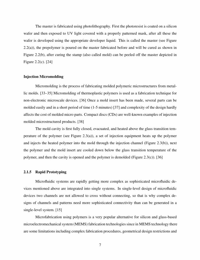
The master is fabricated using photolithography. First the photoresist is coated on a silicon
wafer and then exposed to UV light covered with a properly patterned mask, after all these the
wafer is developed using the appropriate developer liquid. This is called the master (see Figure
2.2(a)), the prepolymer is poured on the master fabricated before and will be cured as shown in
Figure 2.2(b), after curing the stamp (also called mold) can be peeled off the master depicted in
Figure 2.2(c). [24]
Injection Micromolding
Micromolding is the process of fabricating molded polymeric microstructures from metal-
lic molds. [33–35] Micromolding of thermoplastic polymers is used as a fabrication technique for
non-electronic microscale devices. [36] Once a mold insert has been made, several parts can be
molded easily and in a short period of time (1-5 minutes) [37] and complexity of the design hardly
affects the cost of molded micro parts. Compact discs (CDs) are well-known examples of injection
molded microstructured products. [38]
The mold cavity is first fully closed, evacuated, and heated above the glass transition tem-
perature of the polymer (see Figure 2.3(a)), a set of injection equipment heats up the polymer
and injects the heated polymer into the mold through the injection channel (Figure 2.3(b)), next
the polymer and the mold insert are cooled down below the glass transition temperature of the
polymer, and then the cavity is opened and the polymer is demolded (Figure 2.3(c)). [36]
2.1.5 Rapid Prototyping
Microfluidic systems are rapidly getting more complex as sophisticated microfluidic de-
vices mentioned above are integrated into single systems. In single-level design of microfluidic
devices two channels are not allowed to cross without connecting, so that is why complex de-
signs of channels and patterns need more sophisticated connectivity than can be generated in a
single-level system. [15]
Microfabrication using polymers is a very popular alternative for silicon and glass-based
microelectromechanical system (MEMS) fabrication technologies since in MEMS technology there
are some limitations including complex fabrication procedures, geometrical design restrictions and
7
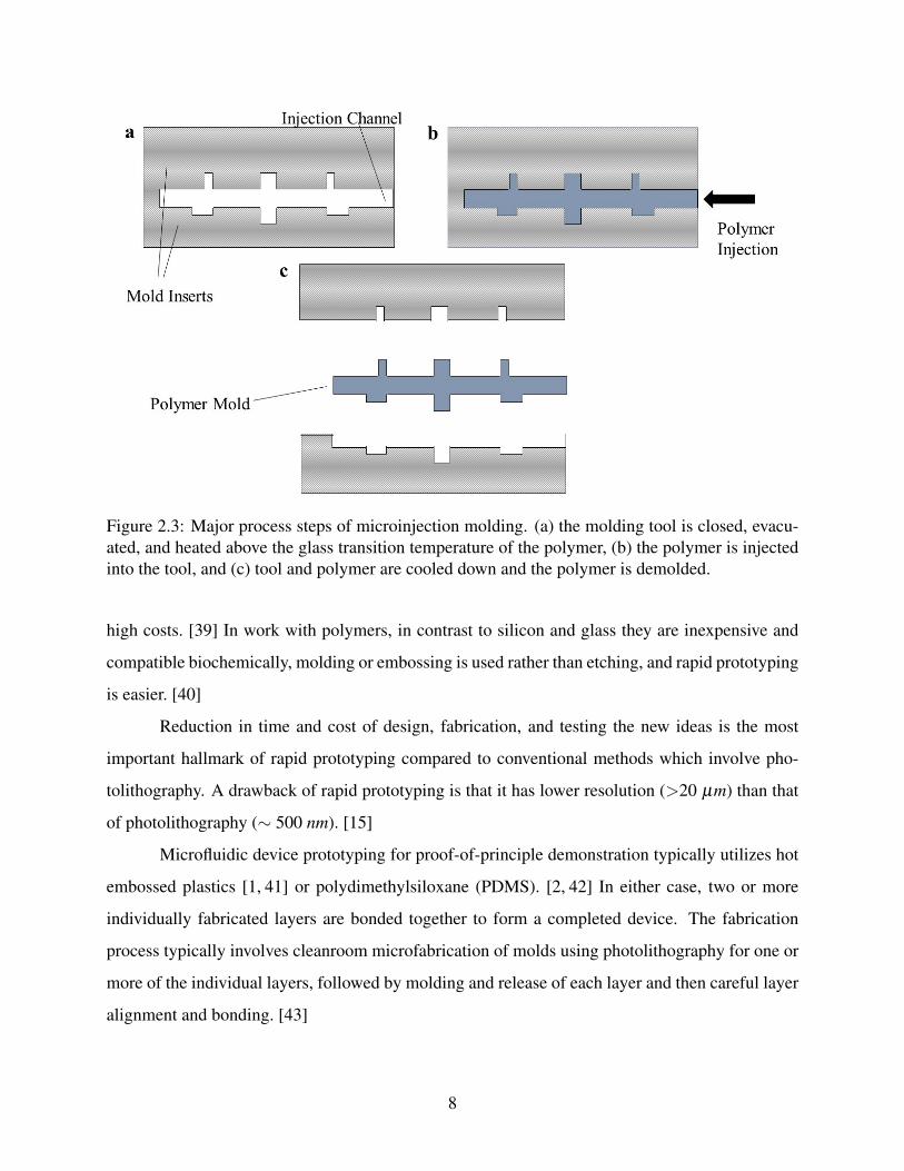
Figure 2.3: Major process steps of microinjection molding. (a) the molding tool is closed, evacu-ated, and heated above the glass transition temperature of the polymer, (b) the polymer is injectedinto the tool, and (c) tool and polymer are cooled down and the polymer is demolded.
high costs. [39] In work with polymers, in contrast to silicon and glass they are inexpensive and
compatible biochemically, molding or embossing is used rather than etching, and rapid prototyping
is easier. [40]
Reduction in time and cost of design, fabrication, and testing the new ideas is the most
important hallmark of rapid prototyping compared to conventional methods which involve pho-
tolithography. A drawback of rapid prototyping is that it has lower resolution (>20 µm) than that
of photolithography (∼ 500 nm). [15]
Microfluidic device prototyping for proof-of-principle demonstration typically utilizes hot
embossed plastics [1, 41] or polydimethylsiloxane (PDMS). [2, 42] In either case, two or more
individually fabricated layers are bonded together to form a completed device. The fabrication
process typically involves cleanroom microfabrication of molds using photolithography for one or
more of the individual layers, followed by molding and release of each layer and then careful layer
alignment and bonding. [43]
8

PDMS is easy to pattern by soft lithography, optically transparent, flexible, gas-permeable,
and cheap enough to be used in copious quantities. These properties make PDMS an excellent
material for the rapid prototyping of microfluidic devices.
The sequence of steps in the fabrication process of microfluidic devices using PDMS often
leads to a delay of one to several weeks between completing the design of a device and actually
having one in hand to test, particularly taking into account the turn-around time to design and
procure photolithographic masks and the inevitable problems that crop up for various steps. [43]
Moreover, limitations in terms of the number of available materials for the prototyping of microflu-
idic systems also hinders their broad development, as problems such as non-specific adsorption that
plague PDMS and other polymers [44, 45], prevent many potential applications from being tested.
2.2 3D-Printing for Microfluidics
Stereolithography (SLA) is an established fabrication technique in manufacturing devices
using a liquid photopolymer resin by means of a focused laser or UV LED light source (Figure
2.4). Microchannels are defined by polymerizing the walls of the channel cavities and subse-
quently draining the residual uncured resin. [46] Note that no alignment or bonding is necessary
to produce 3D structures, which substantially simplifies the processing with respect to soft lithog-
raphy (especially for complex devices). [6] Low manufacturing cost, short fabrication time, and
high aspect ratio (x:y) are the most important characteristics of SLA. Due to dead volume in the
microfluidic devices using conventional fabrication, more materials are used and more space is
occupied, but SLA decreases the dead volume as well as manufacturing time and assembly time.
Investigations on alignment, cleaning, and dicing have shown that microfluidic devices are feasible
to be integrated with SLA. [47, 48] Note that researchers so far have used the commercial resins
provided for the 3D-Printers but we have developed our resin using appropriate materials discussed
in Chapters 4 and 5.
Figure 2.4 depicts a schematic outline of how a structure is printed using stereolithographic
3D printing. First the resin is dumped onto a designed build tray for the printer shown in Figure
2.4(a), after setting up the printer the build table approaches the bottom of the build tray and then
the UV LED turns on for a specific exposure time and is exposed on the build table patterned by a
9

Figure 2.4: Principles of stereolithographic 3D printing. (a) the resin is poured in the build trayand the build table starts to approach the build tray, and (b) the UV LED is turned on for a specificexposure time on the build table, and (c) again it moves upward to its first position in the first step.
CAD software (see Figure 2.4(b)), then the build table moves upward and a layer of the structure
is printed (Figure 2.4(c)).
Comparison between (a) PDMS/plastic molding and (b) stereolithography depicted in Fig-
ure 2.5 shows the path to commercialization. [6]
In the case of PDMS soft lithography is used as the fabrication method for microfluidic
devices which was explained in Figure 2.5 in the previous section, then a startup company that
is interested in producing the commercial form of a PDMS or glass prototype (see Figure 2.5(a))
will have to develop a plastic-molding process that is entirely different than the original soft litho-
graphic one, as depicted schematically in Figure 2.2. This issue is not a big deal for the basic
one-layer devices but it can be a major challenge for more complex and multi-layer devices with
many design features. Therefore the costs for producing such complex commercial form of PDMS
will rise and as a result the potential investors are not convinced whether the profits obtained from
future sales can recover the initial investment in a reasonable time. As opposed to plastic microflu-
idic devices produced by soft lithography or other methods, with SLA the design process is directly
initiated in plastic, optimized in plastic, and can directly be transferred to the licensing company
once it is suitable for production, as shown schematically in Figure 2.5(b). [6]
10

Figure 2.5: Comparison between (a) PDMS/plastic molding and (b) stereolithography showing thepath to commercialization.
2.2.1 Different 3D-Printers, Price and Resolution (X-Y/Z)
Table 2.2 shows the resolution and price of different desktop stereolithography systems.
The mechanism of their light source is also given in the table. [6]
In my previous research B9Creator was used as the printer to print the microdevices due to
decent resolution and lower expenses. It worked perfect for our work in terms of having functional
valves and my first paper was published on that. B9Creators lamp was a projector which gave out
white light. It brought about so many problems in terms of having all the colors in the spectrum
and due to the materials using in our resin (to be discussed in the next chapter) the products were
colored as orange. Obviously printing orange products can lead to bulk fluorescence and it influ-
ences the experiment with biomaterial samples. In order to eliminate that issue we bought an Asiga
11

Table 2.2: Comparison of desktop stereolithography systems. The properties for the printers areup to January 2014.
Technology X-Y resolution Open-source PriceAsiga Pico systems DLP 27-39 µm No $6990-$8990EnvisionTEC Micro DLP 31 µm No 12 999
B9Creator DLP 50-100 µm Yes $2990-$4995MiiCraft DLP 56 µm Yes $1999
3D Systems ProJet 1200 DLP 56 µm No $4900Formlabs Form 1 LASER 300 µm No $3299
Pico 3D-Printer which has a UV LED projector instead of a consumer projector with a white light
source. The downside about Asiga is that it is not open-source compared to B9Creator.
2.3 Resin Formulation
Resins utilized in stereolithography are typically composed of 3 main components: (1)
monomer, (2) photoinitiator, and (3) absorber. They need to be mixed properly in order to achieve
consistent device printing. In terms of concentration, the formulation must be adjusted to produce
the optimum polymerization and ideal feature properties. For instance if the photoinitiator concen-
tration is too low there will not be enough free radicals (to be explained in Section 2.3.2) to excite
the monomer, and as a result the polymerization will not take place. Conversely, if the photoinitia-
tor concentration is too high this may cause the free radicals to react with each other and terminate
the polymerization so the product may not be polymerized completely, may polymerize in shorter
chains terminating prematurely, or even overpolymerize.
2.3.1 Monomer
Monomers are generally small organic molecules that can join with other similar molecules
to form very large chains, or polymers. All monomers have the capacity to form chemical bonds
to at least two other monomer molecules. Polymerization of monomers is initiated through a
photoinitiator (to be discussed in the next section) which creates a radical monomer. The radical
site of one monomer reacts with a different monomer molecule to form a chemical bond, creating a
new radical in the second monomer unit. This process continues until two radicals come together at
12

Figure 2.6: Molecular structure of polyethylene glycol diacrylate (PEGDA)
which point the polymerization stops. Polymerization typically occurs through the double bonds in
the monomer [49] with methacrylate functional groups being one of the most common monomers.
[50] In my work polyethylene glycol diacrylate (PEGDA) (depicted in Figure 2.6) is used as the
monomer.
2.3.2 Photoinitiator (PI)
There are some important terms related to polymerization and photoinitiators which need
to be defined properly in order to fully understand the process of photoinitiators. Some of the most
essential terms are defined in Table 2.3.
The polymerization process begins with PI absorbing light (typically UV light) to form a
free radical. [51] These free radicals react with the monomer to create a monomer free radical.
The monomer free radical then comes in contact with non-radical monomer molecule and they
react to start the curing (polymerization) process. [52] This curing continues through free radicals
reacting with double bonds of monomer causing chain reactions and polymerization and continues
until two free radicals come in contact together. [53] It is already known that different PIs absorb
UV light at different wavelengths. Here in order to have a chain reaction and polymerization PIs
λmax should be similar (within a few nanometers) to the UV lamp’s emission spectrum maximum
in order to have optimal absorbance of light leading to optimal polymerization.
Having the correct amount of PI in the solution is critical. The correct amount leads to
chain reactions and polymerization as desired. As discussed the PI begins the curing process in
a step called initiation. Too much PI could result in premature polymer termination reactions.
Initiation and termination processes are described here.
13
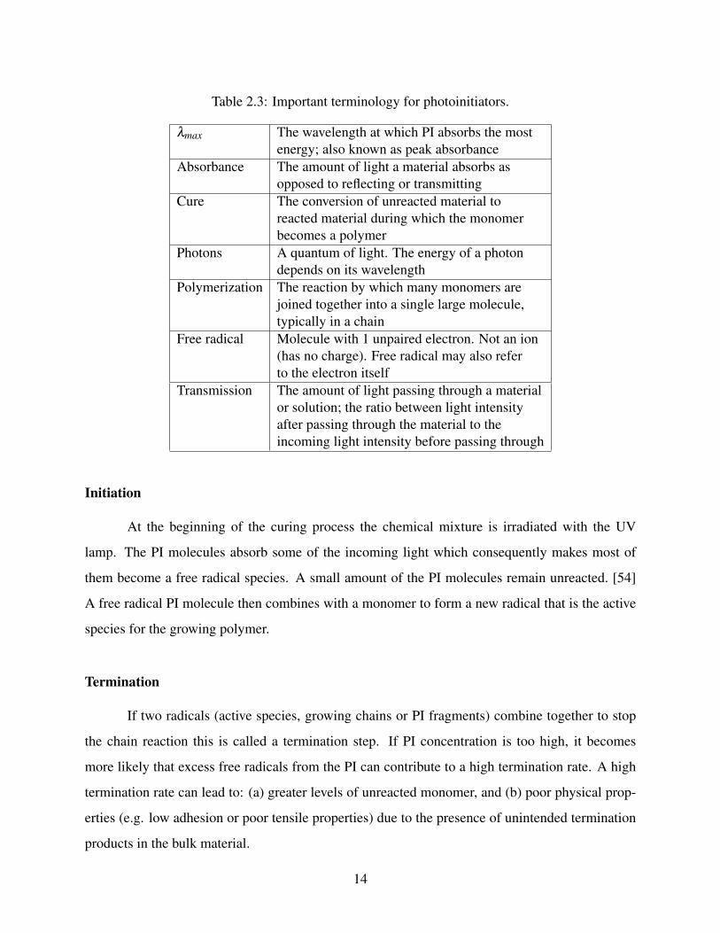
Table 2.3: Important terminology for photoinitiators.
λmax The wavelength at which PI absorbs the mostenergy; also known as peak absorbance
Absorbance The amount of light a material absorbs asopposed to reflecting or transmitting
Cure The conversion of unreacted material toreacted material during which the monomerbecomes a polymer
Photons A quantum of light. The energy of a photondepends on its wavelength
Polymerization The reaction by which many monomers arejoined together into a single large molecule,typically in a chain
Free radical Molecule with 1 unpaired electron. Not an ion(has no charge). Free radical may also referto the electron itself
Transmission The amount of light passing through a materialor solution; the ratio between light intensityafter passing through the material to theincoming light intensity before passing through
Initiation
At the beginning of the curing process the chemical mixture is irradiated with the UV
lamp. The PI molecules absorb some of the incoming light which consequently makes most of
them become a free radical species. A small amount of the PI molecules remain unreacted. [54]
A free radical PI molecule then combines with a monomer to form a new radical that is the active
species for the growing polymer.
Termination
If two radicals (active species, growing chains or PI fragments) combine together to stop
the chain reaction this is called a termination step. If PI concentration is too high, it becomes
more likely that excess free radicals from the PI can contribute to a high termination rate. A high
termination rate can lead to: (a) greater levels of unreacted monomer, and (b) poor physical prop-
erties (e.g. low adhesion or poor tensile properties) due to the presence of unintended termination
products in the bulk material.
14
2.3.3 Absorber
A UV absorber is introduced to the resin mixture as the final component. An appropriate
UV absorber is chosen by looking at the absorbance spectrum for the UV absorber and photoini-
tiator, and the emission spectrum of the light source. The UV absorber should have considerable
absorbance in the regions where the PI and light source overlap. Typically the absorbance of the
PI is usually less than that of UV absorber in the region of their mutual absorbance. Therefore by
adding a small amount of UV absorber to the mixture I can decrease the amount of byproducts in
the polymerization process. The UV absorber will absorb some of the light that would have created
photoinitiator free radicals which in turn means fewer free radicals will be in the polymerization
mixture leading to fewer termination steps. Otherwise the unintended termination products can
cause bulk material problems such as undesired device fluorescence or improper curing. The un-
desired device fluorescence can be problematic because it may influence the fluorescence measured
when the devices are used with actual samples.
In the next Chapter, the 3D-Printer used for my research will be discussed and then in
Chapter 4 and 5 the resin formulations utilized for the 3D- Printer will be presented.
15

CHAPTER 3. ASIGA 3D-PRINTER
In this chapter, I outline the set of equipment used in my research. I then discuss design
fabrication procedures of the device.
3.1 Asiga Pico27 3D-Printer
Asiga Pico27 is the 3D printer I used in order to complete this thesis. The light source is
a UV LED lamp working at 385 nm, and the mechanism for this LED is digital light processing
(DLP) as given in Table 2.2. The emission spectrum of the LED will be discussed in next chapter.
UV LED, slider, Teflon build tray, and build table are the main components of the printer. The
purpose of each part will be discussed briefly here in Sections 3.1.1 and 3.1.2.
3.1.1 Calibration
The slider is placed under the build tray to level the bottom of the tray with the top of the
build table. The purpose of the slider will be discussed in the next section. Using the instruction
provided along with the printer, the slider should be calibrated and leveled properly with the build
table. Z-axis should also be calibrated in order to set the zero point position.
3.1.2 Operation of Printer
Here the operation of the printer will be briefly described. Once the printer is turned on, the
slider should be calibrated and z-axis zero position should be set properly using the instructions
given above. After the calibrations are done, the design prepared in an automatic STL & SLC
support and build preparation package called Asiga Composer will be uploaded on the hard drive
of the printer and then the print will be started. First the resin is poured in the Teflon film tray, the
print command is given and the build table then approaches the tray and the slider moves to the
16

other side to level out the bottom of the tray with the build table. Next after the resin is exposed for
a specified exposure time causing a polymerized layer on the build table, it separates from the tray
and rises for about 7 mm. There is a delay called wait time in which the build table stops at the
top so that the polymerized device cools down and then approaches the build tray for printing the
next layer. This can be specified in the Asiga composer software. A cube with 5 mm height takes
18 minutes to be printed completely with 10 seconds exposure time for the 2 initial layers and 0.2
seconds for subsequent layers.
3.2 Die Design
As seen in Figure 3.1 a designed microvalve consists of several important parts which are
integrated in OpenSCAD a 3D computer-aided design (CAD) software useful in designing com-
plex 3D structures. The device is designed with a simple suspended membrane over a valve cham-
ber as depicted in Figures 3.1(a) and 3.1(b). The control chamber is located above the membrane
and two cross channel lines connect the two external ports to this chamber. The reason for having
two ports is once the structure is printed it can be drained more easily through these two ports.
Another two ports one called inlet and other called outlet are placed to enable introducing fluid
into the valve chamber. The operating mechanism for the valve is, once the sample is introduced
into the fluid channel, the valve can be closed by applying pressure to both control ports to deflect
the membrane down which seals the fluid channel. Alternatively, one can seal one of the control
ports and apply pressure to the other for the similar effect.
Figure 3.2 shows the complete design getting printed each time I run the printer. There are
four major components in the design as depicted in Figure 3.2(a). Components 1, 2, and 3 are the
microvalves designed with different membrane sizes as schematically shown in Figure 3.2. The
left valve, middle valve, and right valve are respectively 1.5 mm, 2 mm, and 3 mm diameter valve
membranes. Component 4 is the design number for each device. Once a design is changed, the
number is updated. Components 5 and 6 are the horizontal cross channels placed in the design
to determine the minimum flow channel sizes. The vertical cylinders are put there so that the
channels can be flushed properly immediately after 3D printing. Component 7 is also a different
kind of resolution pattern which can help find the minimum feature size between each two vertical
17

Figure 3.1: Valve schematic. (a) Top view and (b) side view schematics of test valve design.The control chamber and fluidic chamber regions are voids in the 3D printed device. The controlchamber has two access ports to enable it to be drained after printing. Pressure can be appliedthrough both ports to actuate the valve, or one channel can be sealed and pressure can be appliedthrough the other to actuate the valve. Pressurized membrane (black dotted line) shows valveclosure.
walls. Figure 3.2(b) shows a finished device printed using Asiga. The left and right valves are
printed but the middle valve is not properly printed.
3.3 Die Fabrication
Figure 3.3 depicts the steps in fabrication of the device schematically. In brief, the printer is
set up first and the design is uploaded on the printer’s hard drive. The build table is then prepared to
approach the build tray (Figure 3.3(a)), next the resin is added to the Teflon build tray and the build
table approaches and stops above the bottom of the build table (Figure 3.3(b)). The projector image
is then focused on the bottom surface of the build table (Figure 3.3(c)), which polymerizes the resin
in the exposed region (Figure 3.3(d)). The projector image is varied layer-by-layer to create the
desired 3D structure uploaded on the printers hard drive (Figure 3.3(e)). When the device is pulled
from the resin bath after all layers are exposed and printed as given in the design, the channels
contain unpolymerized resin (Figure 3.3(f)). Flushing out of the structure with isopropyl alcohol
(IPA) leaves a finished device (see Figure 3.2).
18
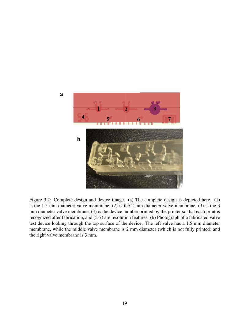
Figure 3.2: Complete design and device image. (a) The complete design is depicted here. (1)is the 1.5 mm diameter valve membrane, (2) is the 2 mm diameter valve membrane, (3) is the 3mm diameter valve membrane, (4) is the device number printed by the printer so that each print isrecognized after fabrication, and (5-7) are resolution features. (b) Photograph of a fabricated valvetest device looking through the top surface of the device. The left valve has a 1.5 mm diametermembrane, while the middle valve membrane is 2 mm diameter (which is not fully printed) andthe right valve membrane is 3 mm.
19

Figure 3.3: Fabrication process. (a) The printer is set up and the build table is prepared to approachthe build tray. (b) Resin is added to the build tray and the build table approaches above the bottomof the build table. (c) The projector image is focused on the bottom surface of the build table,which (d) polymerizes the resin in the exposed region. (e) The projector image is varied layer-by-layer to create the desired 3D structure. (f) When the device is pulled from the bath after all layersare printed, the channels contain unpolymerized resin; this must be drained from the structure,resulting in a finished device (see Figure 3.2(b)).
20

CHAPTER 4. RESIN FORMULATION I
4.1 Chemicals Present in the Resin Formulation
In this chapter I discuss the resin formulation that I utilized in my research. There are
three main components including monomer, UV absorber, and photoinitiator (PI) that I defined in
Chapter 2. These components are combined to cause polymerization once exposed to UV light.
Before I discuss the materials used in this research, I introduce the UV LED that I used as
the light source for initiating the polymerization process. Unfortunately I have not been able to
measure the spectrum of the UV LED since our spectrometer was not working, but a typical UV
LED like Thorlabs M385L2 LED has a peak wavelength of 385 nm. Figure 4.1 shows the emission
spectrum of the LED in which the vertical axis is normalized intensity.
4.1.1 Monomer
Polyethylene glycol diacrylate (PEGDA) with a molecular weight of 258 g/mol (see Figure
4.2) is present as the monomer and it is polymerized once combined with the photoinitiator and
exposed to UV light as discussed in Chapter 3.
4.1.2 Photoinitiator
The first photoinitiator used in this thesis is diphenyl(2,4,6-trimethylbenzoyl)phosphine
oxide (TMDPO) with a molecular structure depicted in Figure 4.3. The absorption spectrum for
TMDPO is given in Figure 4.1. I used this PI because it absorbs well at 385 nm although it has
higher absorption at short wavelengths.
21

Figure 4.1: Spectrum of the UV absorber, the PI, and the UV LED.
Figure 4.2: PEGDA molecular structure
4.1.3 UV Absorber
Liquid hydroxyphenyl-benzotriazole commercially called BLS-99 is added to the solution
as the UV absorber. Figure 4.4 shows the molecular structure of BLS- 99. The absorption spectrum
for BLS-99 (depicted in Figure 4.1) shows that this absorber is absorptive at 385 nm, although it
has higher absorption at shorter wavelengths. The absorption spectrum of BLS-99 has been plotted
for 20 mg/L in ethyl acetate.
22

Figure 4.3: TMDPO molecular structure
Figure 4.4: BLS-99 molecular structure
4.2 Resin Formulation
The first prepolymer resin was prepared by mixing 1% (w/w) TMDPO and 0.18% (w/w)
BLS-99 in PEGDA (M.W. 258) and sonicated in an ultrasound bath for 35 minutes. Table 4.1
shows different solution concentrations which were used as the resin formulation for Asiga. The
reason 1% TMDPO and 0.18% BLS-99 were chosen as a starting point because we had used
23

Table 4.1: Different solution concentrations used for this research.
Solution Number TMDPO (%) BLS-99 (%) Exposure times (s)1 1.0 0.18 0.6, 0.3, 0.152 2.0 0.18 0.4, 0.3, 0.2, 0.15, 0.13 3.5 0.18 0.6, 0.3, 0.2, 0.154 3.1 1.00 0.15, 0.13, 0.125 3.1 1.50 0.15, 0.126 4.0 1.50 0.2, 0.15, 0.12, 0.17 5.1 2.00 0.15, 0.12, 0.18 6 1.00 0.13, 0.19 10 1.00 0.11, 0.1
10 8 1.00 0.1, 0.09, 0.08, 0.07
these solution concentrations in the previous work using a B9creator 3D printer. [43] Sudan I and
Phenylbis (2,4,6-trimethylbenzoyl) phosphine oxide (Irgacure 819) were used respectively as the
UV absorber and the PI for that work.
According to Table 4.1, high concentrations of TMDPO and BLS-99 were tested with
different exposure times as well as low concentrations. Based on results and observations It turned
out that higher concentrations of TMDPO and BLS-99 in PEGDA are more suitable in terms of
printing functional valves and internal resolution features. The reason is higher concentrations of
photoinitiator and UV absorber prevents the light to penetrate deeper in the solution. This results in
printing successful voids and chambers inside the device. Therefore, solutions with (6% TMDPO,
1% BLS-99 concentrations), (10% TMDPO, 1% BLS-99 concentrations), and (8% TMDPO, 1%
BLS-99 concentrations) were made and tested. In Section 4.3 the results are discussed.
4.3 Results
Figure 4.5 shows the image for the printed device with (6% TMDPO, 1% BLS-99 concen-
trations). None of the valves are functional since the control lines are sealed and not connected to
the control chambers. But in Figure 4.6 in which (10% TMDPO, 1% BLS-99 concentrations) are
used in printing this finished device, it is observed that two of the valves are completely printed.
The valves were tested if the membranes were deflecting once control pressure was applied and
they were functional. Although the left part of the device was not printed due to termination steps.
24
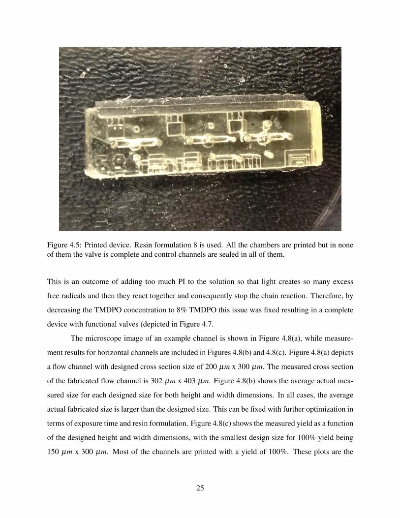
Figure 4.5: Printed device. Resin formulation 8 is used. All the chambers are printed but in noneof them the valve is complete and control channels are sealed in all of them.
This is an outcome of adding too much PI to the solution so that light creates so many excess
free radicals and then they react together and consequently stop the chain reaction. Therefore, by
decreasing the TMDPO concentration to 8% TMDPO this issue was fixed resulting in a complete
device with functional valves (depicted in Figure 4.7.
The microscope image of an example channel is shown in Figure 4.8(a), while measure-
ment results for horizontal channels are included in Figures 4.8(b) and 4.8(c). Figure 4.8(a) depicts
a flow channel with designed cross section size of 200 µm x 300 µm. The measured cross section
of the fabricated flow channel is 302 µm x 403 µm. Figure 4.8(b) shows the average actual mea-
sured size for each designed size for both height and width dimensions. In all cases, the average
actual fabricated size is larger than the designed size. This can be fixed with further optimization in
terms of exposure time and resin formulation. Figure 4.8(c) shows the measured yield as a function
of the designed height and width dimensions, with the smallest design size for 100% yield being
150 µm x 300 µm. Most of the channels are printed with a yield of 100%. These plots are the
25
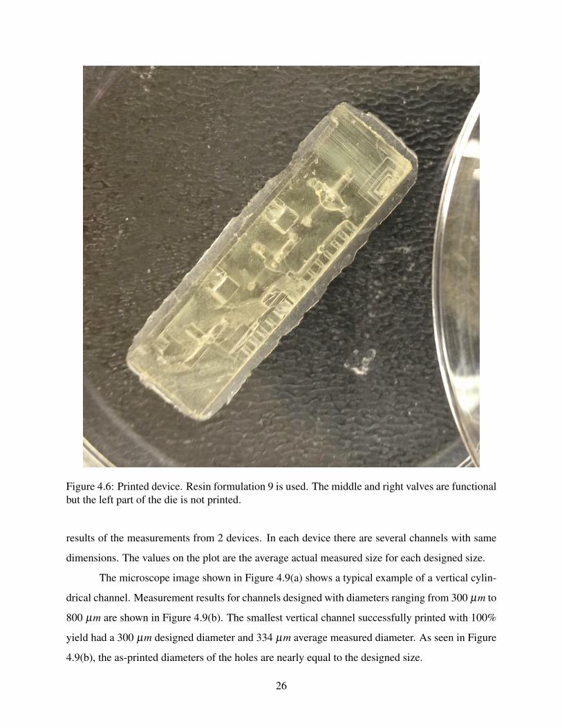
Figure 4.6: Printed device. Resin formulation 9 is used. The middle and right valves are functionalbut the left part of the die is not printed.
results of the measurements from 2 devices. In each device there are several channels with same
dimensions. The values on the plot are the average actual measured size for each designed size.
The microscope image shown in Figure 4.9(a) shows a typical example of a vertical cylin-
drical channel. Measurement results for channels designed with diameters ranging from 300 µm to
800 µm are shown in Figure 4.9(b). The smallest vertical channel successfully printed with 100%
yield had a 300 µm designed diameter and 334 µm average measured diameter. As seen in Figure
4.9(b), the as-printed diameters of the holes are nearly equal to the designed size.
26

Figure 4.7: Printed device. Resin formulation 10 is used. The left and right valves are functional.
4.4 Discussion
TMDPO was not a good choice because too much of it is required in order to print func-
tional valves and have acceptable internal and exterior resolution features. Too much PI in the
resin produces lots of byproduct once exposed to UV light. These byproducts can cause undesired
device fluorescence which is problematic because it will influence the background fluorescence of
27

Figure 4.8: Horizontal channel fabrication, repeatability, and yield. (a) Side view of a flow channelwith designed cross section size of 200 µm x 300 µm. The measured cross section of the fabricatedflow channel is 302 µm x 403 µm. (b) Average actual (measured) flow channel size as a functionof the designed size (error bars show standard deviation based on measurement of 2 samples). (c)Yield as a function of the designed height and width dimension sizes for 2 devices (a couple ofchannels with same dimensions are present in each device) where yield represents the frequencyof a successfully printed open channel.
the device when the device is used with the actual samples. Moreover too much TMDPO makes
the printed devices tend to be more yellowish.
BLS-99 was also not ideally suited to the purposes of this printed device due to low ab-
sorption at 385 nm, even though it works fine for wavelengths ranging from 280 nm to 360 nm as
seen in Figure 4.1. Low absorption causes deeper penetration of light and as a result the chambers
will be sealed.
The second problem is chambers in a designed device are not printed completely and they
are sealed. This makes BLS-99 a bad choice because it does not absorb light above 400 nm as
depicted in Figure 4.1 but TMDPO absorbs light up to 420 nm and the UV LED emits light ap-
proximately up to 410 nm. Since the LED does not emit light above 410 nm, the wavelengths above
28

Figure 4.9: Vertical cylindrical channel fabrication, repeatability, and yield. (a) Top view of adesigned 550 µm cylindrical channel. The measured diameter of the channel is 564 µm. (b)Actual (measured) cylindrical channel size as a function of the designed size. Successfully printedopen channels (yield) as a function of the designed cylinder diameters. Error bars denote standarddeviation based on measurement of four channels (300-450 µm holes) and eight channels (500-800µm holes).
410 nm are not important. The range between 400 nm and 410 nm causes the second problem since
in this range the UV absorber does not absorb light but TMDPO has a decent absorption seen in
Figure 4.1. Imagine there is a design like Figure 4.10. There are two chambers separated by a
membrane. Two ports are added to the design so that at the end of the print the unpolymerized
resin can be flushed out. Once the bottom chamber is printed, the light is exposed on the device
and it forms the membrane. According to the emission spectrum of UV LED, it emits light around
400 nm-410 nm too. The UV absorber does not absorb light around these wavelengths so light
penetrates deeper and makes the bottom chamber get polymerized. The same process takes place
to the top chamber and it will be sealed. Eventually a sealed device is printed. This could be
adjusted by decreasing exposure time which has been done a lot in this thesis but on the other hand
the external features and some internal features will be misshaped.
Based on what I discussed and concluded, I decided to look for better choices of PI and
UV absorber. In the next chapter the second resin formulation used in this project will be studied.
29

Figure 4.10: Two designed chambers separated by a membrane and two ports to flush the unpoly-merized design out of the chambers at the end of the print.
30
CHAPTER 5. RESIN FORMULATION II
5.1 Materials
In Chapter 4, I concluded that the PI (TMDPO) and the UV absorber (BLS-99) were not
well-suited for my research due to several reasons. In brief, too much TMDPO in the solution
results in a finished device with lots of unintended byproducts. Moreover absorption spectrum of
BLS-99 does not match with that of the UV LED and the PI for wavelengths over 400 nm and at
385 nm its absorption is too low causing deeper penetration of light. These were the main reasons
I changed the materials in order to get better external and internal features with reasonably small
concentrations of UV absorber and PI.
5.1.1 Photoinitiator
In our previous work [43] phenylbis (2,4,6-trimethylbenzoyl) phosphine oxide (Irgacure
819) was used as the PI. The purple curve in Figure 5.1 shows the absorption spectrum for PI.
At 385 nm the absorption for Irgacure 819 is higher than absorption of TMDPO for the same
concentration in PEGDA (see Figure 4.1). The only downside about Irgacure 819 is its absorption
in visible light region. Therefore all the experiments using uncured resin with Irgacure 819 have
been done in darkened room.
5.1.2 UV Absorber
After an extensive search for a new UV absorber, one was found which more closely
matched the UV LED emission spectrum. The blue curve in Figure 5.1 shows the absorption
spectrum for 2-(2’-Hydroxy-3’-tert-butyl-5’-methylphenyl)-5-chlorobenzortriazole (UV 326). It
is also observed that at 385 nm the absorption for UV 326 is greater than the absorption of BLS-99
31

Figure 5.1: Spectrum of the UV absorber, the PI, and the UV LED.
approximately with a factor of 4. The absorption spectrum of UV 326 has been plotted for 10 mg/L
in chloroform.
5.2 Quantitative Analysis of Polymerization Depth as a Function of Layer Exposure Time
5.2.1 Definitions
Irradiance, I(z),(W/cm2) as a function of depth, z:
I(z) = I0e−αz, (5.1)
Dose, D(z, t),(J/cm2) as a function of depth, z, and exposure time per layer, tl:
D(z, t) = tlI(z) (5.2)
= tlI0e−αz. (5.3)
32

Figure 5.2: Normalized irradiance as a function of depth.
Let’s examine several arbitrary absorption coefficients, α1 and α2 in units of µm−1. Fig-
ure 5.2 depicts the normalized irradiance as a function of depth for α1 =1
100µm and α2 =1
25µm .
Now look at what happens to the dose as a function of depth for different layer exposure
times in Figure 5.3. Since dose is irradiance multiplied by layer exposure time, the higher the
exposure time, the higher the dose. For an arbitrary critical dose shown as a black dashed horizontal
line, the polymerization depth for the α = 125µm case and tl = 1s and tl = 2s is less than 50 µm, and
as a result the layers do not stick together since the layer thickness is designed to be 50 µm, but for
the α = 125µm case and tl = 4s the depth is slightly higher than 50 µm, therefore, the layers stick
together resulting in a solid polymerized device. For the α = 1100µm case and tl = 1s for the same
critical dose the depth is around 75 µm. This also results in a solid polymerized device but since
the depth is higher than 50 µm, the light will penetrate deeper. Consequently the unpolymerized
resin inside the chambers becomes solidified so the chambers will be almost sealed.
5.2.2 Relationship Between Depth and Exposure Time for a Given Critical Dose
The critical dose, Dc, at which polymerization has proceeded far enough to result in a solid
material can be written as
Dc = tlI0e−αzd , (5.4)
33
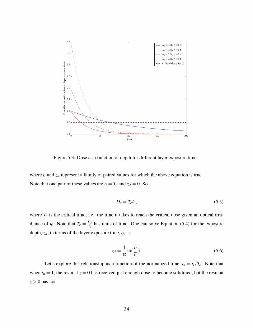
Figure 5.3: Dose as a function of depth for different layer exposure times.
where tl and zd represent a family of paired values for which the above equation is true.
Note that one pair of these values are tl = Tc and zd = 0. So
Dc = TcI0, (5.5)
where Tc is the critical time, i.e., the time it takes to reach the critical dose given an optical irra-
diance of I0. Note that Tc =DcI0
has units of time. One can solve Equation (5.4) for the exposure
depth, zd , in terms of the layer exposure time, tl , as
zd =1α
ln(tlTc). (5.6)
Let’s explore this relationship as a function of the normalized time, tn = tl/Tc. Note that
when tn = 1, the resin at z = 0 has received just enough dose to become solidified, but the resin at
z > 0 has not.
34
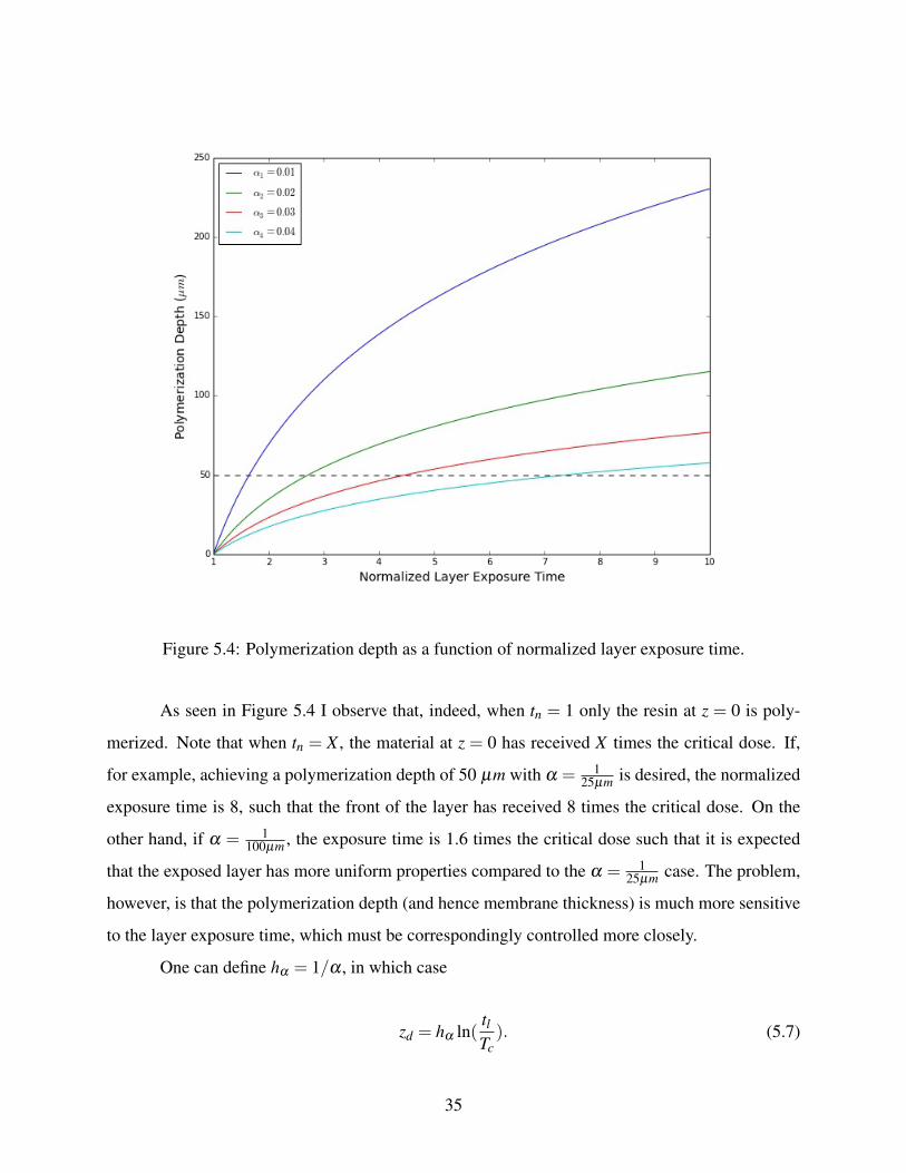
Figure 5.4: Polymerization depth as a function of normalized layer exposure time.
As seen in Figure 5.4 I observe that, indeed, when tn = 1 only the resin at z = 0 is poly-
merized. Note that when tn = X , the material at z = 0 has received X times the critical dose. If,
for example, achieving a polymerization depth of 50 µm with α = 125µm is desired, the normalized
exposure time is 8, such that the front of the layer has received 8 times the critical dose. On the
other hand, if α = 1100µm , the exposure time is 1.6 times the critical dose such that it is expected
that the exposed layer has more uniform properties compared to the α = 125µm case. The problem,
however, is that the polymerization depth (and hence membrane thickness) is much more sensitive
to the layer exposure time, which must be correspondingly controlled more closely.
One can define hα = 1/α , in which case
zd = hα ln(tlTc). (5.7)
35

Moreover,
αz =z
hα
(5.8)
= zn, (5.9)
where zn is the normalized distance into the resin. One can rewrite the polymerization depth as
zn = ln(tn). (5.10)
Note that when zn = 1 (i.e., z = hα ) the dose is such that the polymerization depth is hα . It’s clear
that when a dose is applied that results in polymerization to a depth of hα , the normalized exposure
time is
tn = ezn=1 (5.11)
= e, (5.12)
such that the z = 0 layer of resin has received a dose that is e = 2.72 times bigger than the critical
dose.
5.3 Results from Experiments
In the following experiments I have used a solution with 1% Irgacure 819 based on previ-
ous work with the B9 creator 3D printer and 1% UV 326. Figure 5.5 depicts the design which is
printed to determine the effect of exposure time on membrane thickness while Figure 5.6(a) shows
a successfully printed device with 50 µm membrane. Figure 5.6(b) shows the measured membrane
thickness as a function of layer exposure time. As expected, longer layer exposure time results
in greater membrane thickness because the empty space behind the membrane is filled with un-
exposed resin. The longer the exposure time, the deeper into this region the polymerization front
advances. Note that this will make the membrane thicker (and therefore stiffer). These experi-
36

Figure 5.5: Designed single-layer membranes (yellow) supported by posts (red) on a 1.5 mm slab(green). (a) Top view, (b) Side view.
ments indicate an exposure time in the range of 0.3 to 0.5 sec/layer works well. Exposures less
than 0.3 sec failed to successfully print due to weak bonding between print layers, and at 0.3 sec
the print layers were easily damaged. On the other hand, exposures greater than 0.5 sec resulted in
overpolymerized devices. With a range of 0.3 to 0.5 sec exposure times, the total 3D printer build
time for a typical 3.1 mm tall x 9.5 mm x 6 mm device is only 10-12 minutes.
From Figure 5.6(b), it can be seen that the straight line with a slope of 280 µm and 0.244
seconds interception with vertical axis fits the points. Comparing these values to Equation (5.7), it
is concluded that hα = 280 µm and Tc = 0.244 seconds.
5.4 Discussion
At the beginning when I started to make solutions, I made some random solutions with dif-
ferent UV 326 concentrations based on my experiences and observations from several experiments
and looking at the spectrums. I kept Irgacure 819 fixed at 1% since it was an appropriate choice
for previous work. I made four solutions with 0.5%, 1%, 2%, and 4% UV 326 and 1% Irgacure
819 concentration. I noticed that 0.5% and 1% UV 326 in PEGDA were soluble but 2% and 4%
37

Figure 5.6: (a) Successfully printed device with 50 µm membrane. (b) Measured membrane thick-ness as a function of layer exposure time. In the design, the membrane thickness is specifiedas a single 3D printed layer. Error bars for data points for all exposure times represent standarddeviation based on measurement of 6 membranes.
were not soluble in PEGDA even after placing the solutions in ultrasound bath for 4 hours. That
was the downside about UV 326. Therefore, better choices of UV absorber is needed with a decent
amount of absorbance at the range of 385 nm. It also needs to be soluble in PEGDA.
38

CHAPTER 6. CONCLUSIONS AND FUTURE WORK
6.1 Conclusions
In this thesis PEGDA is utilized in 3D printing using an Asiga 3D printer. Chapter 3 con-
tains the operation of Asiga and fabrication process of 3D printed valves in microfluidic systems.
In Chapter 4, TMDPO and BLS-99 were used respectively as the photoinitiator and the UV ab-
sorber. Devices up to 5-mm-tall, containing 3D printed microfluidic channels with valves ≤ 1.5
mm diameter, were printed in under 20 minutes. Horizontal flow channels with cross sections
down to 150 µm x 300 µm and vertical cylindrical channels as small as 300 µm in diameter were
printed with a 100% yield. In Chapter 5, Irgacure 819 and UV 326 were used respectively as the
photoinitiator and the UV absorber. Membrane thickness was studied as a function of layer expo-
sure time; the membrane thickness increased as exposure was lengthened due to polymerization
of resin in the void underneath the membrane. Under-exposure of the polymer layers resulted in
brittle, unbound layers, whereas over-exposure caused overpolymerization and thicker membrane.
6.2 Future Work
Due to TMDPO chosen for the 3D printing resin in Chapter 4, since its absorption is too
low at 385 nm once mixed with PEGDA, the fabricated devices have lots of unintended byproducts
which affect the fluorescence out of the device once used with actual samples. To solve this issue,
TMDPO was replaced by Irgacure 819 which had been used in our previous work. It has a higher
absorption at 385 nm but it also has absorption at visible light region, so fabrication should be done
in a dark room. Therefore, these should be adjusted for later works by providing a PI with high
absorption at 385 nm and no absorption in visible light region.
The BLS-99 working as UV absorber in Chapter 4 was not appropriate mostly due to low
absorption at 385 nm and also no absorption from 400-410 nm. This caused deeper penetration
39

of light and consequently smaller or sealed chambers. UV 326 used in Chapter 5 had higher
absorption at 385 nm but it was insoluble in PEGDA for concentrations higher than 1%. As a
result, another appropriate UV absorber should be chosen in which the absorption is higher than
the previous ones and it is also soluble in PEGDA for concentrations higher than 1%.
In Chapter 4 and 5, 3D printed valves were designed and printed but they were not tested
although I printed some successful devices. The problem with those devices was, the metal pins
placed in the inlets and outlets were so loose that they could not stay there by themselves. This
made it impossible to test the valves since they needed to tolerate 10-30 PSI control pressure. Valve
pressure tests need to be done as future research in which the fluid pressure should be studied as a
function of control pressure.
Resin development is the novel aspect of this thesis and once an appropriate set of UV
absorber and photoinitiator are found, it enables us to print microfluidic devices and use them in
applications such as biosensing.
40
REFERENCES
[1] Q. Mei, Z. Xia, F. Xu, S. A. Soper, and Z. H. Fan, “Fabrication of microfluidic reactors andmixing studies for luciferase detection,” Analytical chemistry, vol. 80, no. 15, pp. 6045–6050,2008. 1, 8
[2] S. K. Sia and G. M. Whitesides, “Microfluidic devices fabricated in poly (dimethylsiloxane)for biological studies,” Electrophoresis, vol. 24, no. 21, pp. 3563–3576, 2003. 1, 8
[3] B. C. Gross, J. L. Erkal, S. Y. Lockwood, C. Chen, and D. M. Spence, “Evaluation of 3dprinting and its potential impact on biotechnology and the chemical sciences,” Analyticalchemistry, vol. 86, no. 7, pp. 3240–3253, 2014. 1
[4] P. J. Kitson, M. H. Rosnes, V. Sans, V. Dragone, and L. Cronin, “Configurable 3d-printed mil-lifluidic and microfluidic lab on a chipreactionware devices,” Lab on a chip, vol. 12, no. 18,pp. 3267–3271, 2012. 1
[5] P. J. Kitson, M. D. Symes, V. Dragone, and L. Cronin, “Combining 3d printing and liq-uid handling to produce user-friendly reactionware for chemical synthesis and purification,”Chemical Science, vol. 4, no. 8, pp. 3099–3103, 2013. 1
[6] A. K. Au, W. Lee, and A. Folch, “Mail-order microfluidics: evaluation of stereolithographyfor the production of microfluidic devices,” Lab on a Chip, vol. 14, no. 7, pp. 1294–1301,2014. 1, 9, 10, 11
[7] A. I. Shallan, P. Smejkal, M. Corban, R. M. Guijt, and M. C. Breadmore, “Cost-effectivethree-dimensional printing of visibly transparent microchips within minutes,” Analyticalchemistry, vol. 86, no. 6, pp. 3124–3130, 2014. 1
[8] C. Xia and N. X. Fang, “3d microfabricated bioreactor with capillaries,” Biomedical microde-vices, vol. 11, no. 6, pp. 1309–1315, 2009. 2
[9] C. Sun, N. Fang, D. Wu, and X. Zhang, “Projection micro-stereolithography using digitalmicro-mirror dynamic mask,” Sensors and Actuators A: Physical, vol. 121, no. 1, pp. 113–120, 2005. 2
[10] X. Zheng, J. Deotte, M. P. Alonso, G. R. Farquar, T. H. Weisgraber, S. Gemberling, H. Lee,N. Fang, and C. M. Spadaccini, “Design and optimization of a light-emitting diode projec-tion micro-stereolithography three-dimensional manufacturing system,” Review of ScientificInstruments, vol. 83, no. 12, p. 125001, 2012. 2
[11] A. Manz, D. J. Harrison, E. M. Verpoorte, J. C. Fettinger, A. Paulus, H. Ludi, and H. M. Wid-mer, “Planar chips technology for miniaturization and integration of separation techniques
41

into monitoring systems: capillary electrophoresis on a chip,” Journal of Chromatography A,vol. 593, no. 1, pp. 253–258, 1992. 3
[12] D. Figeys and D. Pinto, “Lab-on-a-chip: a revolution in biological and medical sciences.”Analytical Chemistry, vol. 72, no. 9, pp. 330–A, 2000. 3
[13] H. Stone and S. Kim, “Microfluidics: basic issues, applications, and challenges,” AIChEJournal, vol. 47, no. 6, pp. 1250–1254, 2001. 4
[14] G. M. Whitesides, “The origins and the future of microfluidics,” Nature, vol. 442, no. 7101,pp. 368–373, 2006. 4
[15] J. R. Anderson, D. T. Chiu, H. Wu, O. J. Schueller, and G. M. Whitesides, “Fabrication ofmicrofluidic systems in poly (dimethylsiloxane),” Electrophoresis, vol. 21, pp. 27–40, 2000.4, 7, 8
[16] C. Zhang, J. Xu, W. Ma, and W. Zheng, “Pcr microfluidic devices for dna amplification,”Biotechnology advances, vol. 24, no. 3, pp. 243–284, 2006. 4
[17] P. Belgrader, C. J. Elkin, S. B. Brown, S. N. Nasarabadi, R. G. Langlois, F. P. Milanovich,B. W. Colston, and G. D. Marshall, “A reusable flow-through polymerase chain reaction in-strument for the continuous monitoring of infectious biological agents,” Analytical chemistry,vol. 75, no. 14, pp. 3446–3450, 2003. 4
[18] Y. Matsubara, K. Kerman, M. Kobayashi, S. Yamamura, Y. Morita, and E. Tamiya, “Mi-crochamber array based dna quantification and specific sequence detection from a single copyvia pcr in nanoliter volumes,” Biosensors and Bioelectronics, vol. 20, no. 8, pp. 1482–1490,2005. 4
[19] U. K. Laemmli et al., “Cleavage of structural proteins during the assembly of the head ofbacteriophage t4,” nature, vol. 227, no. 5259, pp. 680–685, 1970. 4
[20] H. Towbin, T. Staehelin, and J. Gordon, “Electrophoretic transfer of proteins from polyacry-lamide gels to nitrocellulose sheets: procedure and some applications,” Proceedings of theNational Academy of Sciences, vol. 76, no. 9, pp. 4350–4354, 1979. 4, 5
[21] B. T. Kurien and R. H. Scofield, “Protein blotting and detection,” Methods in molecularbiology, vol. 536, no. 356, p. 357, 2009. 4
[22] E. Southern, “Southern blotting,” Nature Protocols, vol. 1, no. 2, pp. 518–525, 2006. 5
[23] Y. Wu, Q. Li, and X. Chen, “Detecting protein–protein interactions by far western blotting,”Nature protocols, vol. 2, no. 12, pp. 3278–3284, 2007. 5
[24] G. M. Whitesides, E. Ostuni, S. Takayama, X. Jiang, and D. E. Ingber, “Soft lithographyin biology and biochemistry,” Annual review of biomedical engineering, vol. 3, no. 1, pp.335–373, 2001. 5, 7
[25] N. Nguyen and S. T. Wereley, Fundamentals and applications of microfluidics. ArtechHouse, 2002. 5
42
[26] M. J. Madou, Fundamentals of microfabrication: the science of miniaturization. CRC press,2002. 6
[27] G. Aumiller, E. Chandross, W. Tomlinson, and H. Weber, “Submicrometer resolution repli-cation of relief patterns for integrated optics,” Journal of Applied Physics, vol. 45, no. 10, pp.4557–4562, 1974. 6
[28] D. J. Beebe, J. S. Moore, Q. Yu, R. H. Liu, M. L. Kraft, B.-H. Jo, and C. Devadoss, “Microflu-idic tectonics: a comprehensive construction platform for microfluidic systems,” Proceedingsof the National Academy of Sciences, vol. 97, no. 25, pp. 13 488–13 493, 2000. 6
[29] J. Choi, S. Kim, R. Trichur, H. J. Cho, A. Puntambekar, R. L. Cole, J. R. Simkins, S. Muruge-san, K. Kim, J.-B. J. Lee et al., “A plastic micro injection molding technique using replace-able mold-disks for disposable microfluidic systems and biochips,” in Micro Total AnalysisSystems 2001. Springer, 2001, pp. 411–412. 6
[30] M. A. Roberts, J. S. Rossier, P. Bercier, and H. Girault, “Uv laser machined polymer sub-strates for the development of microdiagnostic systems,” Analytical Chemistry, vol. 69,no. 11, pp. 2035–2042, 1997. 6
[31] Y. Xia and G. M. Whitesides, “Soft lithography,” Annual review of materials science, vol. 28,no. 1, pp. 153–184, 1998. 6
[32] D. Qin, Y. Xia, and G. M. Whitesides, “Soft lithography for micro-and nanoscale patterning,”Nature protocols, vol. 5, no. 3, pp. 491–502, 2010. 6
[33] M. Niggemann, W. Ehrfeld, and L. Weber, “Fabrication of miniaturized biotechnical devices,”in Micromachining and Microfabrication. International Society for Optics and Photonics,1998, pp. 204–213. 7
[34] L. Weber and W. Ehrfeld, “Micro-moulding-processes, moulds, applications.” Kunststoffe-Plast Europe, vol. 88, no. 10, pp. 1791–1797, 1998. 7
[35] U. M. Attia, S. Marson, and J. R. Alcock, “Micro-injection moulding of polymer microfluidicdevices,” Microfluidics and nanofluidics, vol. 7, no. 1, pp. 1–28, 2009. 7
[36] M. Heckele and W. Schomburg, “Review on micro molding of thermoplastic polymers,” Jour-nal of Micromechanics and Microengineering, vol. 14, no. 3, p. R1, 2004. 7
[37] R. Chien, “Micromolding of biochip devices designed with microchannels,” Sensors andActuators A: Physical, vol. 128, no. 2, pp. 238–247, 2006. 7
[38] V. Piotter, T. Hanemann, R. Ruprecht, and J. Hausselt, “Injection molding and related tech-niques for fabrication of microstructures,” Microsystem Technologies, vol. 3, no. 3, pp. 129–133, 1997. 7
[39] H. Becker and U. Heim, “Hot embossing as a method for the fabrication of polymer highaspect ratio structures,” Sensors and Actuators A: Physical, vol. 83, no. 1, pp. 130–135,2000. 8
43

[40] J. Narasimhan and I. Papautsky, “Polymer embossing tools for rapid prototyping of plasticmicrofluidic devices,” Journal of Micromechanics and Microengineering, vol. 14, no. 1, p. 96,2004. 8
[41] P. N. Nge, C. I. Rogers, and A. T. Woolley, “Advances in microfluidic materials, functions,integration, and applications,” Chemical reviews, vol. 113, no. 4, pp. 2550–2583, 2013. 8
[42] J. Friend and L. Yeo, “Fabrication of microfluidic devices using polydimethylsiloxane,”Biomicrofluidics, vol. 4, no. 2, p. 026502, 2010. 8
[43] C. I. Rogers, K. Qaderi, A. T. Woolley, and G. P. Nordin, “3d printed microfluidic deviceswith integrated valves,” Biomicrofluidics, vol. 9, no. 1, p. 016501, 2015. 8, 9, 24, 31
[44] B. Huang, H. Wu, S. Kim, and R. N. Zare, “Coating of poly (dimethylsiloxane) with n-dodecyl-β -d-maltoside to minimize nonspecific protein adsorption,” Lab Chip, vol. 5, no. 10,pp. 1005–1007, 2005. 9
[45] J. J. Shah, J. Geist, L. E. Locascio, M. Gaitan, M. V. Rao, and W. N. Vreeland, “Surfacemodification of poly (methyl methacrylate) for improved adsorption of wall coating polymersfor microchip electrophoresis,” Electrophoresis, vol. 27, no. 19, pp. 3788–3796, 2006. 9
[46] H. Kang, I. H. Lee, and D. Cho, “Development of an assembly-free process based on virtualenvironment for fabricating 3d microfluidic systems using microstereolithography technol-ogy,” Journal of manufacturing science and engineering, vol. 126, no. 4, pp. 766–771, 2004.9
[47] D. W. Rosen, “Stereolithography and rapid prototyping,” in BioNanoFluidic MEMS.Springer, 2008, pp. 175–196. 9
[48] L. Tse, P. Hesketh, D. Rosen, and J. Gole, “Stereolithography on silicon for microfluidics andmicrosensor packaging,” Microsystem Technologies, vol. 9, no. 5, pp. 319–323, 2003. 9
[49] G. Tan, Y. Wang, J. Li, and S. Zhang, “Synthesis and characterization of injectable pho-tocrosslinking poly (ethylene glycol) diacrylate based hydrogels,” Polymer bulletin, vol. 61,no. 1, pp. 91–98, 2008. 13
[50] C. Nason, T. Roper, C. Hoyle, and J. A. Pojman, “Uv-induced frontal polymerization ofmultifunctional (meth) acrylates,” Macromolecules, vol. 38, no. 13, pp. 5506–5512, 2005. 13
[51] P. Gottschalk, D. C. Neckers, and G. B. Schuster, “As photoinitiators capable of absorbingvisible light and producing free radicals,” Jan. 23 1990, uS Patent 4,895,880. 13
[52] J. Moon, Y. Shul, H. Han, S. Hong, Y. Choi, and H. Kim, “A study on uv-curable adhesives foroptical pick-up: I. photo-initiator effects,” International journal of adhesion and adhesives,vol. 25, no. 4, pp. 301–312, 2005. 13
[53] V. Georges and H. Kazmeier, “Free radical polymerization,” Macromolecules, vol. 26, p.5316, 1993. 13
[54] M. Bae, R. A. Gemeinhart, R. Divan, K. J. Suthar, and D. C. Mancini, “Fabrication of poly(ethylene glycol) hydrogel structures for pharmaceutical applications using electron beam
44

and optical lithography,” Journal of Vacuum Science & Technology B, vol. 28, no. 6, pp.C6P24–C6P29, 2010. 14
45