polymer optical waveguide with multiple graded- index … optical waveguide with multiple...
TRANSCRIPT

Polymer optical waveguide with multiple graded-index cores for on-board interconnects
fabricated using soft-lithography
Takaaki Ishigure* and Yosuke Nitta
Department of Applied Physics and Physico-Informatics, Faculty of Science and Technology, Keio University, 3-14-1, Hiyoshi, Kohoku-ku, Yokohama 223-8522, Japan
Abstract: We successfully fabricate a polymer optical waveguide with multiple graded-index (GI) cores directly on a substrate utilizing the soft-lithography method. A UV-curable polymer (TPIR-202) supplied from Tokyo Ohka Kogyo Co., Ltd. is used, and the GI cores are formed during the curing process of the core region, which is similar to the preform process we previously reported. We experimentally confirm that near parabolic refractive index profiles are formed in the parallel cores (more than 50 channels) with 40 µm x 40 µm size at 250-µm pitch. Although the loss is still as high as 0.1 ~0.3 dB/cm at 850 nm, which is mainly due to scattering loss inherent to the polymer matrix, the scattering loss attributed to the waveguide’s structural irregularity could be sufficiently reduced by a graded refractive index profile. For comparison, we fabricate step-index (SI)-core waveguides with the same materials by means of the same process. Then, we evaluate the inter-channel crosstalk in the SI- and GI-core waveguides under almost the same conditions. It is noteworthy that remarkable crosstalk reduction (5 dB and beyond) is confirmed in the GI-core waveguides, since the propagating modes in GI-cores are tightly confined near the core center and less optical power is found near the core cladding boundary. This significant improvement in the inter-channel crosstalk allows the GI-core waveguides to be utilized for extra high-density on-board optical interconnections.
©2010 Optical Society of America
OCIS codes: (250.5460) Polymer waveguides; (200.4650) Optical interconnects.
References and links
1. A. F. Benner, M. Ignatowski, J. Kash, D. M. Kuchta, and M. Ritter, “Exploitation of optical interconnects in future server architectures,” IBM J. Res. Develop. 49(4), 755–773 (2005).
2. D. M. Kuchta, Y. H. Kwark, C. Schuster, C. Baks, C. Haymes, J. Schaub, P. Pepeljugoski, L. Shan, R. John, D. Kucharski, D. Rogers, M. Ritter, J. Jewell, L. A. Graham, K. Schrödinger, A. Schild, and H.-M. Rein, “120-Gb/s VCSEL-based parallel-optical interconnect and custom 120-Gb/s testing station,” J. Lightwave Technol. 22(9), 2200–2212 (2004).
3. N. Hendrickx, J. Van Erps, G. Van Steenberge, H. Thienpont, and P. Van Daele, “Laser ablated micromirrors for printed circuit board integrated optical interconnections,” IEEE Photon. Technol. Lett. 19(11), 822–824 (2007).
4. S. Kopetz, D. Cai, E. Rabe, and A. Neyer, “PDMS-based optical waveguide layer for integration in electrical–optical circuit boards,” AEU, Int. J. Electron. Commun. 61(3), 163–167 (2007).
5. M. Karppinen, T. Alajoki, A. Tanskanen, K. Kataja, J.-T. Mäkinen, K. Kautio, P. Karioja, M. Immonen, and J. Kivilahti, “Parallel optical interconnect between ceramic BGA packages on FR4 board using embedded waveguides and passive optical alignments,” in Proceedings of IEEE Conference on the 56th Electronic Components and Technology Conference, (IEEE 2006), pp. 219–225.
6. S. Nakagawa, Y. Taira, H. Numata, K. Kobayashi, K. Terada, and M. Fukui, “High-bandwidth, chip-based optical interconnects on waveguide-integrated SLC for optical off-chip I/O,” in Proceedings of IEEE Conference on the 59th Electronic Components and Technology Conference, (IEEE 2009) pp. 2086–2091.
7. T. Ishigure, and Y. Takeyoshi, “Polymer waveguide with 4-channel graded-index circular cores for parallel optical interconnects,” Opt. Express 15(9), 5843–5850 (2007), http://www.opticsinfobase.org/oe/abstract.cfm?id=134364.
#128238 - $15.00 USD Received 11 May 2010; revised 10 Jun 2010; accepted 11 Jun 2010; published 16 Jun 2010(C) 2010 OSA 21 June 2010 / Vol. 18, No. 13 / OPTICS EXPRESS 14191

8. Y. Takeyoshi, and T. Ishigure, “High-density 2 x 4 channel polymer optical waveguide with graded-index circular cores,” J. Lightwave Technol. 27(14), 2852–2861 (2009).
9. X. Wang, L. Wang, W. Jiang, and R. T. Chen, “Hard-molded 51 cm long waveguide array with a 150 GHz bandwidth for board-level optical interconnects,” Opt. Lett. 32(6), 677–679 (2007).
10. T. Ishigure, A. Horibe, E. Nihei, and Y. Koike, “High-bandwidth, high-numerical aperture graded-index polymer optical fiber,” J. Lightwave Technol. 13(8), 1686–1691 (1995).
11. D. Marcuse, Principles of Optical Fiber Measurements, (Academic, 1981). 12. T. Ishigure, S. Tanaka, E. Kobayashi, and Y. Koike, E. Kobayashi, Y. Koike, “Accurate refractive index
profiling in a graded-index plastic optical fiber exceeding gigabit transmission rates,” J. Lightwave Technol. 20(8), 1449–1456 (2002).
13. T. Kosugi, and T. Ishigure, “Polymer parallel optical waveguide with graded-index rectangular cores and its dispersion analysis,” Opt. Express 17(18), 15959–15968 (2009), http://www.opticsinfobase.org/oe/abstract.cfm?uri=oe-17-18-15959.
14. H. Tsushima, E. Watanabe, S. Yoshimatsu, S. Okamoto, T. Oka, and K. Imoto, “Novel manufacturing process of waveguide using selective photobleaching of polysilane films by UV light irradiation,” Proc. SPIE 5246, 119–130 (2003).
15. Y. Kokubun, and M. Koshiba, “Novel multi-core fibers for mode division multiplexing: proposal and design principle,” IEICE Electron. Express 6(8), 522–528 (2009), http://www.jstage.jst.go.jp/article/elex/6/8/6_522/_article.
16. I. Papakonstantinou, D. R. Selviah, R. C. A. Pitwon, and D. Milward, “Low-cost, precision, self-alignment technique for coupling laser and photodiode arrays to polymer waveguide arrays on multilayer PCBs,” Trans. Adv. Packag. 31(3), 502–511 (2008).
17. N. Bamiedakis, J. Beals IV, R. V. Penty, I. H. White, J. V. DeGroot, Jr., and T. V. Clapp, “Cost-effective multimode polymer waveguides for high-speed on-board optical interconnects,” J. Quantum. Electron. 45(4), 415–424 (2009).
18. H. H. Hsu, and T. Ishigure, “High-density channel alignment of graded index core polymer optical waveguide and its crosstalk analysis with ray tracing method,” Opt. Express 18(13), 13368 (2010), http://www.opticsinfobase.org/oe/abstract.cfm?uri=oe-18-13-13368.
1. Introduction
As computing performance has continued to evolve rapidly, optical interconnections including on-board communications have been drawing much attention [1,2]. In particular, multimode polymer optical waveguides integrated on printed circuit boards (PCBs) have been one of the potential candidates for feasible, low-cost interconnection media. Hence, intensive efforts have been made for realizing the on-board integration of polymer optical waveguides [3–6]. In most cases, the polymer optical waveguides have rectangular-shaped cores with step refractive index (SI) profile, because they have been fabricated by means of the conventional photo lithography or imprinting processes.
On the other hand, we have reported to apply polymer optical waveguides with multiple graded-index (GI) cores to on-board optical interconnections [7,8]. In our previous papers, we demonstrated that the parabolic refractive index profiles (GI cores) led to excellent optical properties: reduction of the scattering loss due to the imperfection on the core-cladding boundary, high-speed transmission capability, and low inter-channel crosstalk under very
narrow pitch (−37 dB in 120 µm pitch). However, the polymer optical waveguides with GI cores were fabricated by means of the “preform method,” and thus, the waveguides were obtained independently of PCBs. The preform method itself is essentially a cost-effective fabrication process compared to the other methods, because the waveguides that are hundreds of meters long are obtained from one preform. The waveguides have to be integrated on PCBs after the waveguides are fabricated, and consequently, the alignment cost of the waveguides has been of great concern. Furthermore, three-dimensionally cross-linked polymer is difficult to use for comprising the waveguide because it has to be heat-drawn from a preform. Hence, the high-temperature resistance of the waveguide has been of another concern. In the case of poly methyl methacrylate (PMMA)-based polymer waveguides, heat-drawing is carried out at a temperature of 200 to 250 °C, which means that the PMMA-based waveguides obtained would be unstable for the lamination and solder reflow processes of PCBs carried out at 200 to 260 °C.
In order to address these problems, in this paper, we utilize a UV-curable and cross-linkable monomer applicable to the imprinting process, from which the GI-core waveguides can be directly fabricated on-board. In the following sections, the fabrication process and
#128238 - $15.00 USD Received 11 May 2010; revised 10 Jun 2010; accepted 11 Jun 2010; published 16 Jun 2010(C) 2010 OSA 21 June 2010 / Vol. 18, No. 13 / OPTICS EXPRESS 14192
characteristics of the waveguides obtained are discussed in detail. As it is also possible to fabricate a normal step-index (SI)-core waveguide with the same material system by adjusting the fabrication process, the advantages of GI-core waveguides over their SI-core counterparts are demonstrated.
2. Fabrication of polymer optical waveguides
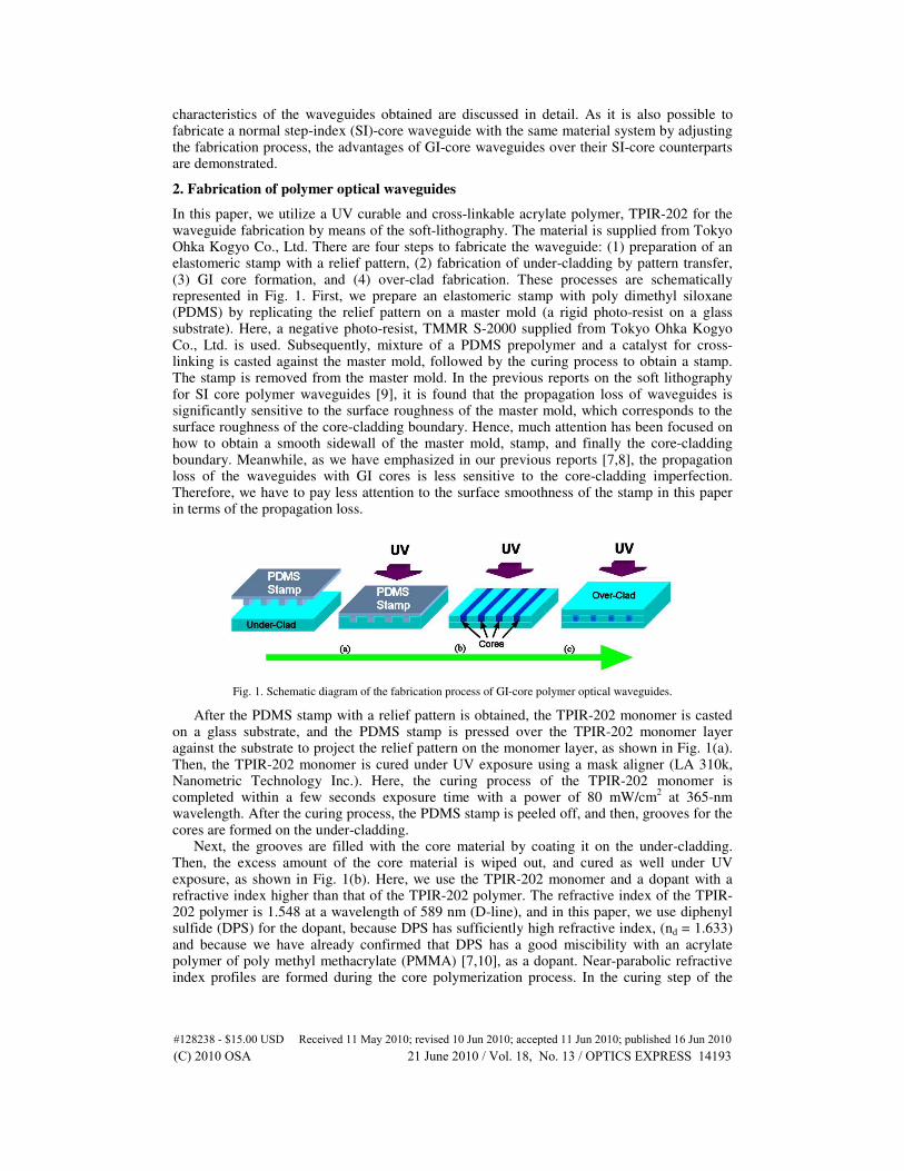
In this paper, we utilize a UV curable and cross-linkable acrylate polymer, TPIR-202 for the waveguide fabrication by means of the soft-lithography. The material is supplied from Tokyo Ohka Kogyo Co., Ltd. There are four steps to fabricate the waveguide: (1) preparation of an elastomeric stamp with a relief pattern, (2) fabrication of under-cladding by pattern transfer, (3) GI core formation, and (4) over-clad fabrication. These processes are schematically represented in Fig. 1. First, we prepare an elastomeric stamp with poly dimethyl siloxane (PDMS) by replicating the relief pattern on a master mold (a rigid photo-resist on a glass substrate). Here, a negative photo-resist, TMMR S-2000 supplied from Tokyo Ohka Kogyo Co., Ltd. is used. Subsequently, mixture of a PDMS prepolymer and a catalyst for cross-linking is casted against the master mold, followed by the curing process to obtain a stamp. The stamp is removed from the master mold. In the previous reports on the soft lithography for SI core polymer waveguides [9], it is found that the propagation loss of waveguides is significantly sensitive to the surface roughness of the master mold, which corresponds to the surface roughness of the core-cladding boundary. Hence, much attention has been focused on how to obtain a smooth sidewall of the master mold, stamp, and finally the core-cladding boundary. Meanwhile, as we have emphasized in our previous reports [7,8], the propagation loss of the waveguides with GI cores is less sensitive to the core-cladding imperfection. Therefore, we have to pay less attention to the surface smoothness of the stamp in this paper in terms of the propagation loss.
Fig. 1. Schematic diagram of the fabrication process of GI-core polymer optical waveguides.
After the PDMS stamp with a relief pattern is obtained, the TPIR-202 monomer is casted on a glass substrate, and the PDMS stamp is pressed over the TPIR-202 monomer layer against the substrate to project the relief pattern on the monomer layer, as shown in Fig. 1(a). Then, the TPIR-202 monomer is cured under UV exposure using a mask aligner (LA 310k, Nanometric Technology Inc.). Here, the curing process of the TPIR-202 monomer is completed within a few seconds exposure time with a power of 80 mW/cm
2 at 365-nm
wavelength. After the curing process, the PDMS stamp is peeled off, and then, grooves for the cores are formed on the under-cladding.
Next, the grooves are filled with the core material by coating it on the under-cladding. Then, the excess amount of the core material is wiped out, and cured as well under UV exposure, as shown in Fig. 1(b). Here, we use the TPIR-202 monomer and a dopant with a refractive index higher than that of the TPIR-202 polymer. The refractive index of the TPIR-202 polymer is 1.548 at a wavelength of 589 nm (D-line), and in this paper, we use diphenyl sulfide (DPS) for the dopant, because DPS has sufficiently high refractive index, (nd = 1.633) and because we have already confirmed that DPS has a good miscibility with an acrylate polymer of poly methyl methacrylate (PMMA) [7,10], as a dopant. Near-parabolic refractive index profiles are formed during the core polymerization process. In the curing step of the
#128238 - $15.00 USD Received 11 May 2010; revised 10 Jun 2010; accepted 11 Jun 2010; published 16 Jun 2010(C) 2010 OSA 21 June 2010 / Vol. 18, No. 13 / OPTICS EXPRESS 14193

under-cladding, we do not cure the monomer completely by adjusting the UV exposure time. Even if the under-cladding is less than half cured, the cladding layer maintains the relief pattern on it, because the TPIR-202 has a cross-linking structure. While the TPIR-202 monomer and DPS molecules filled in the grooves are able to diffuse into the cladding layer. Finally, a concentration distribution of DPS is formed in the core region, which corresponds to the graded refractive index profile. The core layer is not cured completely, since we also need to form a gradual refractive index distribution at the boundary of core and the over-cladding.
In the final step, the over-cladding is formed using the TPIR-202 monomer, as shown in Fig. 1(c), and whole the waveguide is completely cured under sufficient UV exposure.
On the other hand, the soft lithography utilized in this paper is capable of fabricating both GI- and SI-core waveguides with the same material system. The way to control the index profile would be quite simple: just adjusting the curing condition of the under-cladding and core region. Hence, we fabricate a waveguide with SI-cores using the same TPIR-202 and DPS system.
3. Characterization of polymer optical waveguides
3.1 Waveguide structure and refractive index profile
The core-cladding structure is confirmed by observing cross-sections of the fabricated waveguides using a digital optical microscope (VHX-500F, Keyence Corp.). Figure 2 shows examples of a cross-sectional view of the waveguides. Here, the core size is deliberately varied from 110 µm to 40 µm, by utilizing PDMS stamps with different pattern sizes. We confirm that multiple rectangular-shaped cores are aligned in parallel in all the waveguides. The PDMS stamps used for fabrication are 3 cm wide and 5 cm long, in which the periodic relief pattern is formed. Although only several cores are seen in Fig. 2, more than 50 channels are simultaneously obtained at one time using this method.
Fig. 2. Cross-sections of polymer parallel optical waveguides fabricated using the soft lithography (a):110 µm x 110 µm GI core (b): 80 µm x 80 µm SI core (c):40 µm x 40 µm GI core
When we completely cure the under-cladding layer, DPS in the core monomer barely diffuses into the cladding layer, and thus, near SI-cores are obtained, as shown in Fig. 2(b). Compared with the cross-sections of the GI cores shown in Figs. 2(a) and 2(c), we can visually confirm the clear boundary between core and cladding, as the abrupt change of the refractive index at the boundary. From the interference fringe pattern measurement described below, we can still find a slight gradation of refractive index at the boundary of the SI-core, but a quantitative analysis of the index profiles shows that the waveguides can be approximated as SI.
The refractive index profiles formed in the core regions are measured using an interferometric microscope (Mizojiri Optics Co.). A very thin slab sample is prepared, and the interferometric slab method is used [11]. Figure 3 shows photographs of the interference fringe pattern observed on a cross-section of the waveguides actually fabricated. As shown in
(a) (b)
(c)
#128238 - $15.00 USD Received 11 May 2010; revised 10 Jun 2010; accepted 11 Jun 2010; published 16 Jun 2010(C) 2010 OSA 21 June 2010 / Vol. 18, No. 13 / OPTICS EXPRESS 14194

Fig. 3, a contour map-like fringe pattern is observed in each core area, which indicates the existence of a gradual refractive index variation. The waveguides shown in Fig. 3 are fabricated using the same PDMS stamp with 50-µm line width, while the dopant concentration in the core is varied. The under-cladding layer of all the samples is cured under the same condition (1 sec. UV exposure time), to confirm the capability of index profile formation through this fabrication process. With increasing the dopant concentration, the number of dark fringes also increases, as shown in Fig. 3. This indicates the large difference of the refractive index between the core and cladding in the waveguide with a high dopant concentration. From the interference fringe patterns shown in Fig. 3, the refractive index profiles are calculated in the horizontal direction, and the results are shown in Fig. 4(a). Here, we focus only on one core, but we find almost the same index profiles are formed in the other cores. As estimated from Fig. 3, the index difference between the core center and cladding strongly depends on the dopant concentration, and even at a concentration of 23 wt.%, the numerical aperture of the waveguide is calculated to be as high as 0.191 from Fig. 4(a). Therefore, the dopant concentration should be at least 25 wt. % for obtaining an NA of 0.2 and beyond. In the case of polymer materials with no cross-linking structure like PMMA, a dopant concentration as high as 25 wt. % may deteriorate the thermal stability and mechanical strength. However, we can adopt this concentration for the TPIR 202 polymer with cross-linking structure.
Fig. 3. Interference fringe pattern observed on a cross-section of slab sample.
Figure 4(b) shows the normalized refractive index profiles shown in Fig. 4(a). It is noteworthy that the normalized index profiles are almost identical even if the dopant concentration is different. Since this normalized index profile is determined by the diffusivity of dopant, we conclude that the curing condition of the under-cladding layer would be the dominant effect on the refractive index profile. Next, we evaluate the refractive index profile dependence on the curing condition of the under-cladding. We fabricate three waveguides samples under different curing condition. The UV exposure conditions for these waveguides are summarized in Table 1. The index profiles of the waveguides are measured and the results are shown in Fig. 5. In the case of the circular-shaped GI-core waveguides previously we reported, the refractive index profiles could be approximated using the power-law form, as a function of the normalized core radius [12]. Therefore, only a one-time measurement in the radial direction was sufficient.
(a) (b)
Fig. 4. (a): Refractive index profile in one core of fabricated polymer waveguides with different dopant concentration (b) and the normalized profiles shown in Fig. 4(a).
#128238 - $15.00 USD Received 11 May 2010; revised 10 Jun 2010; accepted 11 Jun 2010; published 16 Jun 2010(C) 2010 OSA 21 June 2010 / Vol. 18, No. 13 / OPTICS EXPRESS 14195
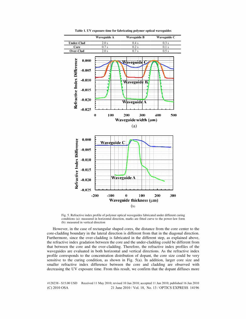
Table 1. UV exposure time for fabricating polymer optical waveguides
Waveguide A Waveguide B Waveguide C
Under-Clad 2.0 s 0.4 s 0.3 s Core 0.7 s 0.2 s 0.1 s
Over-Clad 2.0 s 0.7 s 0.5 s
Fig. 5. Refractive index profile of polymer optical waveguides fabricated under different curing conditions (a): measured in horizontal direction, marks are fitted curve to the power-law form (b): measured in vertical direction
However, in the case of rectangular shaped cores, the distance from the core center to the core-cladding boundary in the lateral direction is different from that in the diagonal direction. Furthermore, since the over-cladding is fabricated in the different step, as explained above, the refractive index gradation between the core and the under-cladding could be different from that between the core and the over-cladding. Therefore, the refractive index profiles of the waveguides are evaluated in both horizontal and vertical directions. As the refractive index profile corresponds to the concentration distribution of dopant, the core size could be very sensitive to the curing condition, as shown in Fig. 5(a). In addition, larger core size and smaller refractive index difference between the core and cladding are observed with decreasing the UV exposure time. From this result, we confirm that the dopant diffuses more
(a)
(b)
#128238 - $15.00 USD Received 11 May 2010; revised 10 Jun 2010; accepted 11 Jun 2010; published 16 Jun 2010(C) 2010 OSA 21 June 2010 / Vol. 18, No. 13 / OPTICS EXPRESS 14196
easily into the less-cured under-cladding, and thus, refractive index profile can be controlled by the curing condition.
Meanwhile, as shown in Fig. 5(a), the refractive index profiles measured in the horizontal direction are almost symmetric, while asymmetric index profiles are found in the vertical direction (Fig. 5(b)). In Fig. 5(b), 0 µm of the horizontal axis (waveguide width) corresponds to the boundary of core and over-cladding area. We observe the steep index variation in the vicinity of the boundary between core and over-cladding in all waveguides compared to that of core and under-cladding. In the case of Waveguide B, the profile in the vertical direction could not be measured because of the abrupt increment of the refractive index. Although the core region is not completely polymerized before the over-cladding layer is casted on it, the dopant cannot diffuse easily from mostly solidified core to the over-cladding. In the following sections, we evaluate the effect of the refractive index profiles on the other optical characteristics of the waveguides.
In order to evaluate the difference in the refractive index profiles in Fig. 5(a), we approximate the measured index profiles by the power-law form described by Eq. (1).
( )
1
2
11 2 0
gr
n r n r aa
= − ∆ ≤ ≤
(1)
where, r is the distance from the core center to the measuring point, n1 is the refractive index at the core center (r = 0), a is the distance from the core center to the core edge, and g is the index exponent. This approximation is generally utilized for circular GI cores, but we already showed in [13] that the refractive index profile in square or rectangular shaped cores also may be approximated by the power law, when the waveguide was fabricated by means of the preform method. Although the index profile formation mechanism is slightly different in the case of the soft-lithography process, the power-law form approximation would also be applicable to the symmetric profiles shown in Fig. 5(a). The best-fit power-law profile to the measured curve is shown by the green and orange points for waveguide A (g = 2.2) and waveguide B (g = 2.7), respectively in Fig. 5(a). For waveguide C, it is difficult to fit a power-law profile.
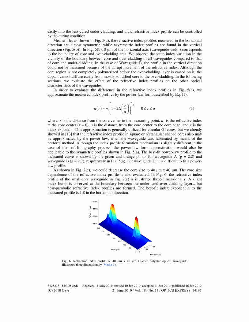
As shown in Fig. 2(c), we could decrease the core size to 40 µm x 40 µm. The core size dependence of the refractive index profile is also evaluated. In Fig. 6, the refractive index profile of the small-core waveguide in Fig. 2(c) is illustrated three-dimensionally. A slight index bump is observed at the boundary between the under- and over-cladding layers, but near-parabolic refractive index profiles are formed. The best-fit index exponent g to the measured profile is 1.8 in the horizontal direction.
Fig. 6. Refractive index profile of 40 µm x 40 µm GI-core polymer optical waveguide illustrated three dimensionally (Media 1).
#128238 - $15.00 USD Received 11 May 2010; revised 10 Jun 2010; accepted 11 Jun 2010; published 16 Jun 2010(C) 2010 OSA 21 June 2010 / Vol. 18, No. 13 / OPTICS EXPRESS 14197
As an index exponent g of 2.0 indicates a perfectly parabolic profile, the index exponent of 1.8 in Fig. 6 is low enough to realize the characteristics expected for GI-core waveguides. Thus, we found a fabrication condition to obtain near-parabolic index profiles, and once the curing condition is optimized, the obtained index profiles show relatively good reproducibility with good core-size uniformity. In addition, in the case of GI-core, the output optical field is more important than the slight amount of core size variation. Therefore, in the next section, we discuss about the relationship between the output near-field pattern (NFP) and the index profile.
3.2 Output near-field pattern
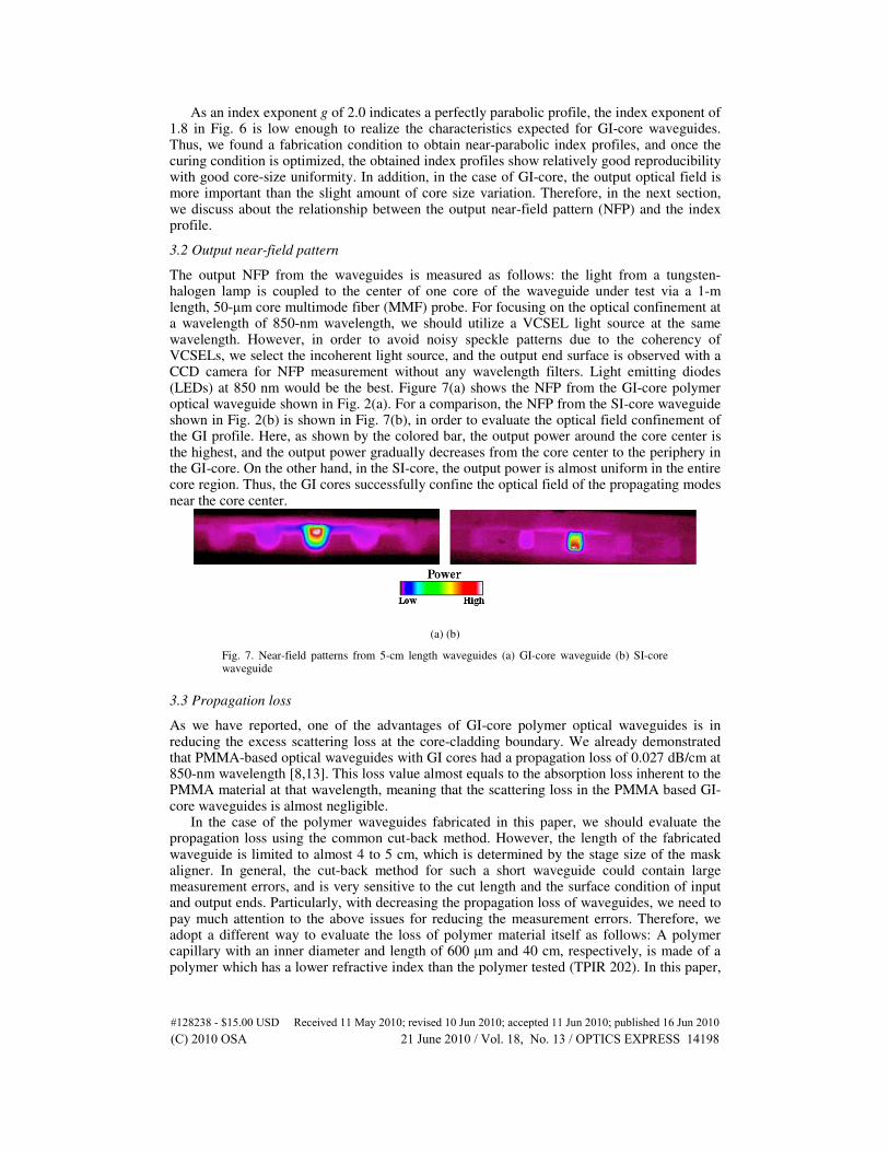
The output NFP from the waveguides is measured as follows: the light from a tungsten-halogen lamp is coupled to the center of one core of the waveguide under test via a 1-m length, 50-µm core multimode fiber (MMF) probe. For focusing on the optical confinement at a wavelength of 850-nm wavelength, we should utilize a VCSEL light source at the same wavelength. However, in order to avoid noisy speckle patterns due to the coherency of VCSELs, we select the incoherent light source, and the output end surface is observed with a CCD camera for NFP measurement without any wavelength filters. Light emitting diodes (LEDs) at 850 nm would be the best. Figure 7(a) shows the NFP from the GI-core polymer optical waveguide shown in Fig. 2(a). For a comparison, the NFP from the SI-core waveguide shown in Fig. 2(b) is shown in Fig. 7(b), in order to evaluate the optical field confinement of the GI profile. Here, as shown by the colored bar, the output power around the core center is the highest, and the output power gradually decreases from the core center to the periphery in the GI-core. On the other hand, in the SI-core, the output power is almost uniform in the entire core region. Thus, the GI cores successfully confine the optical field of the propagating modes near the core center.
(a) (b)
Fig. 7. Near-field patterns from 5-cm length waveguides (a) GI-core waveguide (b) SI-core waveguide
3.3 Propagation loss
As we have reported, one of the advantages of GI-core polymer optical waveguides is in reducing the excess scattering loss at the core-cladding boundary. We already demonstrated that PMMA-based optical waveguides with GI cores had a propagation loss of 0.027 dB/cm at 850-nm wavelength [8,13]. This loss value almost equals to the absorption loss inherent to the PMMA material at that wavelength, meaning that the scattering loss in the PMMA based GI-core waveguides is almost negligible.
In the case of the polymer waveguides fabricated in this paper, we should evaluate the propagation loss using the common cut-back method. However, the length of the fabricated waveguide is limited to almost 4 to 5 cm, which is determined by the stage size of the mask aligner. In general, the cut-back method for such a short waveguide could contain large measurement errors, and is very sensitive to the cut length and the surface condition of input and output ends. Particularly, with decreasing the propagation loss of waveguides, we need to pay much attention to the above issues for reducing the measurement errors. Therefore, we adopt a different way to evaluate the loss of polymer material itself as follows: A polymer capillary with an inner diameter and length of 600 µm and 40 cm, respectively, is made of a polymer which has a lower refractive index than the polymer tested (TPIR 202). In this paper,
#128238 - $15.00 USD Received 11 May 2010; revised 10 Jun 2010; accepted 11 Jun 2010; published 16 Jun 2010(C) 2010 OSA 21 June 2010 / Vol. 18, No. 13 / OPTICS EXPRESS 14198

we use PMMA for the capillary. The capillary is filled with the TPIR 202 monomer using the capillary effect, and then the monomer inside the capillary is cured under UV exposure. Finally, we obtain a polymer optical fiber (POF) with a length of approximately 20 ~30 cm for a loss evaluation, which is suitable for the cut-back method with higher accuracy. However, as the POF does not have a GI profile but an SI structure, the loss reduction effect due to GI core cannot be evaluated.
The light from a tungsten-halogen lamp is coupled to the POF under test via a 1-m silica based multimode fiber with a 400-µm core diameter, and the output end is butt-coupled to an 800-µm core multimode fiber probe to guide all the output light into an optical spectrum analyzer (ANDO, AQ-6328B). The result of the cut-back process at a wavelength of 850 nm is shown in Fig. 8(a). In the case of the TPIR 202 polymer, the loss is calculated to be 0.36 dB/cm from the slope in Fig. 8(a), which is too large even for short-range on-board applications. Here, the TPIR 202 polymer initially had a yellow color attributed to the color of the photo initiator. Therefore, the concentration of the initiator was optimized for reducing the yellow color. A POF was fabricated using the TPIR 202 by adding the optimized concentration of initiator, and then the propagation loss of the POF was also evaluated. As shown by the blue marks in Fig. 8(a), the propagation loss at 850 nm is remarkably reduced to 0.12 dB/cm.
Generally, it is believed that the absorption loss due to a slight yellow color in a polymer would not influence the propagation loss particularly at a wavelength of 850 nm, because the absorption peak of the yellow-colored polymer is at 450 nm and shorter. Therefore, some polymer materials such as polyimide and poly silane are utilized for conventional polymer waveguides, despite having a slight yellow color. In fact, those waveguides exhibit low propagation loss at 850 nm [14]. On the other hand, the results shown in Fig. 8 indicate that reduction of yellow color from polymer waveguides is effective for decreasing the propagation loss to the level of 0.1 dB/cm at 850-nm wavelength. It I also recognized that the effect of yellow color is extremely reduced in the TPIR 202 with optimized initiator by comparing the propagation losses at a wavelength shorter than 900 nm shown in Fig. 8(b). Since the POFs fabricated in this paper have an SI profile as mentioned above, the loss reduction by the GI-profile is not involved in the results shown in Fig. 8. Therefore, it is anticipated that the loss in the GI-core waveguides would be lower than the results of SI-core POF in Fig. 8.
(a) (b)
Fig. 8. Propagation loss of SI-core polymer optical waveguides (a): Results of cut-back process (b): Loss spectra of waveguides fabricated under different conditions
3.4 Inter-channel crosstalk
The origin of the inter-channel crosstalk observed in multimode polymer optical waveguides could be divided into two categories: mode coupling and mode conversion. Power transition due to mode coupling is well utilized in 3 dB couplers in which the inter-core pitch of two cores is so small that the evanescent wave of the mode in one core could interact with the other core. Recently, the inter-channel crosstalk due to mode coupling has been discussed in designing a new multi-core single-mode fiber [15]. On the other hand, the crosstalk in current
#128238 - $15.00 USD Received 11 May 2010; revised 10 Jun 2010; accepted 11 Jun 2010; published 16 Jun 2010(C) 2010 OSA 21 June 2010 / Vol. 18, No. 13 / OPTICS EXPRESS 14199

multimode polymer optical waveguides is mainly caused by the mode conversion, because their pitch is generally as wide as 250 µm. Here, the mode conversion could be from the cladding modes to propagating modes in the core, due to the light scattering inherent to the polymer material or structural imperfections. However, little attention had been paid to the inter-channel crosstalk in polymer parallel optical waveguides. Meanwhile, some recent reports focus on the crosstalk in SI-core waveguides [16,17] in order to evaluate the capability of smaller core and narrower pitch design, but the relationship between the crosstalk and scattering loss is still unclear. As mentioned above, the scattering loss of the TPIR 202-based waveguides fabricated in this paper is higher than that of PMMA, and thus, the influence of the scattering loss on the crosstalk could be investigated using the new waveguides.
The inter-channel crosstalk in both GI-core and SI-core waveguides is experimentally measured as follows: One channel of the waveguides is launched via a single-mode fiber (SMF) probe or a 50-µm core GI-MMF probe, and then the output light from the core of the 5-cm long waveguide is coupled to another 50-µm core GI-MMF probe to guide it to an optical power meter. Here, a VCSEL light source at 850 nm is used, hence the SMF probe with an approximately 10-µm diameter is supposed to correspond to a direct butt-coupling of a waveguide and a VCSEL chip. The MMF probe for the detection is scanned horizontally on the cross-section and the output power is monitored at each position. The output-power difference from the centers of the neighboring core and the launched core is defined as the crosstalk. In the case of the waveguide with 27-wt.% DPS doped, the NA of MMF detection probe could be lower than that of the waveguide, by which output power filtration due to the lower NA would be of concern. However, the case of a waveguide-MMF-ribbon connection would actually exist for board-to-board interconnection. Therefore, the crosstalk is evaluated with this setup despite the NA mismatch.
Figure 9 compares the results of GI-core and SI-core waveguides in which 21 wt. % of DPS is doped. The crosstalk values obtained from Fig. 9 are summarized in Table 2, where the NA dependence of the crosstalk in GI-core waveguides is also shown by evaluating the waveguides with 27-wt.% DPS. When we dope 21 wt. % of DPS, the NA reaches 0.19, while an NA of 0.23 is realized for 27 wt. %. As shown in Fig. 9 and Table 2, we observe a distance dependence of the crosstalk: the nearest cores show larger crosstalk than the other cores apart from the launched core.
We were able to compare the crosstalk in the SI- and GI-core waveguides fabricated by the same process with the same material system, for the first time to the best of our knowledge.
Fig. 9. Inter-channel crosstalk measurement results of 1-m length GI- and SI-core waveguides.
#128238 - $15.00 USD Received 11 May 2010; revised 10 Jun 2010; accepted 11 Jun 2010; published 16 Jun 2010(C) 2010 OSA 21 June 2010 / Vol. 18, No. 13 / OPTICS EXPRESS 14200

Although the crosstalk values in all the channels are higher than those of GI-core waveguides previously evaluated [8], we observe a noticeable trend that the crosstalk values in the SI-core waveguides are 5~10 dB higher than those in the GI-core waveguides, as shown in Table 2. In particular, it is interesting that the launch-condition dependence (SMF or MMF) of the crosstalk is more obvious in the GI-core waveguide. Furthermore, lower crosstalk is observed in high-NA GI-core waveguide (27 wt.% DPS doped), than in the 21 wt.% DPS doped counterpart. These results are attributed to the optical field confinement by the GI-core, as mentioned in section 3.2. As we mentioned in section 3.3, the propagation los of the TPIR-202 based waveguides are currently as low as 0.12 dB at 850-nm wavelength, which is mainly attributed to the excess scattering loss inherent to the TPIR-202 polymer. Hence, such a high scattering loss increases the crosstalk value compared to those in PMMA-based waveguides we previously reported. Therefore, in order to decrease the crosstalk, reduction of the excess scattering loss not only from the core-cladding boundary but inherent to the polymer material would be the key issue. Currently we are theoretically estimating the relationship between the scattering loss and the inter-channel crosstalk in polymer optical waveguides. The preliminary results are described in [18].
Table 2. Comparison of crosstalk value in GI-core and SI-core waveguides under different launch conditions.
Waveguide Probe Ch. 1 Ch. 2 Ch. 4 Ch. 5 SI Core
SMF −19.1 dB −16.3 dB −12.6 dB −17.5 dB
GI Core −32.0 dB −23.2 dB −22.3 dB −29.2 dB
SI Core GI MMF
−17.4 dB −15.3 dB −14.8 dB −16.8 dB GI Core −25.9 dB −20.7 dB −19.2 dB −23.7 dB
GI Core (27wt.%)
SMF −40.1 dB −29.2 dB −29.8 dB −41.9 dB GI MMF −25.1 dB −20.5 dB −20.9 dB −25.0 dB
4. Conclusion
We succeeded in fabricating a polymer parallel waveguide with GI cores by means of the soft-lithography method. Although the propagation loss of the fabricated waveguide is still as high as 0.1 ~0.3 dB/cm at a wavelength of 850 nm, the waveguides show the unique optical properties of GI-cores, such as optical confinement of propagating mode fields, and low inter-channel crosstalk. In terms of the propagation loss, optimization of the photo initiator concentration for lowering the yellow color led to a remarkable loss decrease even at 850-nm wavelength. Further improvement in the polymer material and photo initiator would make it possible to decrease the loss to less than 0.1 dB/cm.
The polymer optical waveguides with GI cores fabricated on-board directly would be a promising solution for chip-to-chip optical interconnections.
Acknowledgments
The authors would like to acknowledge Mr. Toshiya Takagi, Mr. Shoji Ohtaka, and Ms. Rie Matsumoto of Tokyo Ohka Kogyo Co., Ltd., for material supply and fruitful technical discussions. The authors also would like to acknowledge Prof. Yoshinori Matsumoto of Keio University for valuable advice on the soft lithography process.
#128238 - $15.00 USD Received 11 May 2010; revised 10 Jun 2010; accepted 11 Jun 2010; published 16 Jun 2010(C) 2010 OSA 21 June 2010 / Vol. 18, No. 13 / OPTICS EXPRESS 14201