porous silicon sensors- elusive and erudites2is.org/issues/v1/n1/papers/paper3.pdf · porous...
TRANSCRIPT
Porous Silicon Sensors- Elusive and Erudite
Prof. H. Saha IC Design & Fabrication Centre
Electronics & Telecommunication Engineering Department Jadavpur University, Kolkata – 700032, India
Telephone: +91 33 24146833 Telefax: +91 33 24146217
E-mail: [email protected]
Abstract: Porous Silicon Sensors have been fabricated and tested successfully over the last
few years as humidity sensors, vapour sensors, gas sensors, piezoresistive pressure sensors
and bio- sensors. In each case it has displayed remarkably sensitivity, relatively low
temperature operation and ease of fabrication. Brief description of fabrication and properties
of all these types of different sensors is reported in this paper. The barriers of porous silicon
like contact, non- uniformity, instability etc. are also discussed.
Keywords: Porous Silicon , Sensing application, Barriers of porous silicon
1.Introduction
Porous silicon is one of the most attractive host platforms for fabrication of large variety of
sensors [1]. Its widely different structures (from macroporous of mesoporous to nanoporous)
having very large surface to volume ratio, ease of fabrication, distributed nature of resistive
capacitance network, natural nanocrystalline quantum wire like behavior and compatibility to
silicon IC technology leading to smart sensors have been fascinating the sensor researchers of
all over the world for more than a decade [2-6]. Extensive work has been reported on
humidity sensors, organic vapour sensors and gas sensors with porous silicon as host material
[5-12]. Porous silicon has also been used as a sacrificial material for the fabrication of inertial
sensors like pressure sensors [13]. Recently it is reported that nanocrystalline porous silicon
exhibits a very high piezoresistivity that can be utilized for the fabrication of high sensitivity
pressure sensors[14-15]. Macroporous silicon based biosensors have been drawing serious
attention of the researchers over the last few years [16-20]. Instantaneous detection and
quantification of bacteria and other organic materials including DNA measured through the
change of the electrical impedance of porous silicon sensor have been reported by several
groups [21].
Inspite of the demonstrated high potential of porous silicon as an excellent host platform for
sensing applications, commercial availability of porous silicon sensors are yet to be realized.
34
INTERNATIONAL JOURNAL ON SMART SENSING AND INTELLIGENT SYSTEMS, VOL. 1, NO. 1, MARCH 2008
The secondary limitations of porous silicon like nonlinearity, temperature sensitivity, drift,
hysteresis etc. can be overcome through ingenious and intelligent electronics that may be
hybridized or integrated with the porous silicon sensor as desired [22-23]. But the primary
limitations of porous silicon originate from the problems of (a) stable ohmic contact (b)
instability of porous silicon material characteristics (c) lack of reproducibility. In this
presentation fabrication of porous silicon and its applications as different types of sensors are
first reported. Various problems associated with porous silicon are then discussed and the
directions of work towards their solutions are pointed out.
2.Formation of Porous Silicon
Porous Silicon can be formed either nanoporous or mesoporous or macroporous structures
depending on the formation parameters and the forming solution. The experimental details for
forming both nanoporous and macroporous porous silicon are reported here.
2.1Nanoporous Silicon
On a p-type monocrystalline silicon wafer of resistivity 1-2Ωcm, porous silicon is formed by
anodic etching method [1]. The anodic bath is composed of a mixture of HF (48%) and
ethanol. The formation current density and time of formation used for anodic etching are 10-
50mA/cm2 and 10-30 minutes respectively. A porosity (P) of around 40- 80% and a thickness
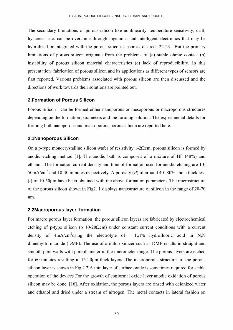
(t) of 10-50μm have been obtained with the above formation parameters. The microstructure
of the porous silicon shown in Fig2. 1 displays nanostructure of silicon in the range of 20-70
nm.
2.2Macroporous layer formation
For macro porous layer formation the porous silicon layers are fabricated by electrochemical
etching of p-type silicon (ρ 10-20Ωcm) under constant current conditions with a current
density of 4mA/cm2using the electrolyte of 4wt% hydrofluoric acid in N,N
dimethylformamide (DMF). The use of a mild oxidizer such as DMF results in straight and
smooth pore walls with pore diameter in the micrometer range. The porous layers are etched
for 60 minutes resulting in 15-20μm thick layers. The macroporous structure of the porous
silicon layer is shown in Fig.2.2 A thin layer of surface oxide is sometimes required for stable
operation of the devices For the growth of conformal oxide layer anodic oxidation of porous
silicon may be done. [16]. After oxidation, the porous layers are rinsed with deionized water
and ethanol and dried under a stream of nitrogen. The metal contacts in lateral fashion on
35
H.SAHA, POROUS SILICON SENSORS- ELUSIVE AND ERUDITE
porous silicon are then deposited by vacuum evaporation followed by gold contacts for wire
bonding.
Fig.2.1 Nanoporous Structure
Fig.2.2 Macroporous structure
3.Vapour Sensors
One of the earliest applications of porous silicon sensors is vapour sensors including humidity
sensors. PS based vapour sensors must fulfill a number of requirements: they have to respond
quickly, sensitively and accurately, their temperature ranges should be as large as possible and
they should have desired selectivity with respect to other vapours or gases. It is well known
that both capacitance and conductance variation of a porous ceramic layer depends very much
on the porosity of the layer. The size and distribution of pores of the ceramic sensors also play
very important role in determining the sensitivity and response time [1]. The porosity and
pore morphology of PS can be varied from mesopores to micropores and to nanopores by
simply controlling its formation parameters like concentration of electrolyte, etching current
density, etching time, bulk doping of the silicon wafer and intensity and wavelength of
illumination [2]. Thus, in PS based vapour sensors, different vapours can be sensed
selectively and sensitively by tailoring the morphology and the corresponding adsorbing
properties of PS sensing layer.
36
INTERNATIONAL JOURNAL ON SMART SENSING AND INTELLIGENT SYSTEMS, VOL. 1, NO. 1, MARCH 2008
3.1Principle of vapour sensing
The working principle of a PS based capacitive vapour sensor is straightforward: vapour
molecules are first adsorbed at the surface of PS transducing layer and then diffuse into the
porous bulk. Condensation of the diffused vapour may occur inside the pores having radii less
than a critical value called Kelvin radius [5]. Due to the differences in permittivity, the
capacitance of the layer changes as a function of the vapour uptake, which is directly related
to the vapour concentration level in the environment [6].
In order to explain the change in dielectric constant of PS layer and provide a theoretical basis
for optimizing the porosity and pore morphology of the PS transducer for sensing a particular
vapour selectively, a theoretical model has been proposed [3]. This model considers PS as a
three-phase (silicon nano-particles, silicon oxides and voids) mixture of dispersed spherical
particles. The sensitivity of PS layer to a particular vapour is due to the adsorption of the
vapour molecules on its surface as well as condensation inside the pores. Thus, the
adsorption-diffusion-condensation kinetics of the vapour molecules inside the porous bulk
and consequently the change in dielectric constant of the porous layer has been modeled with
a generalized effective medium approximation (GEMA )
3.2Fabrication of humidity sensor
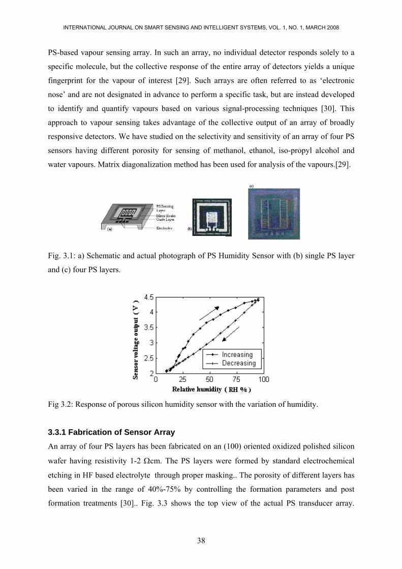
Fig. 3.1 (a), (b) show respectively the schematic and actual photograph of PS humidity
sensor. PS layer of 1cm X 1cm area has been fabricated on a p-type (100) (1-2 .cm resistivity)
oxidized and polished silicon wafer by standard electrochemical etching method [1]. The
formation current density and HF concentration in electrolyte were 10 mA/cm2 and 24%
respectively and the sample was anodized for 3 minutes to achieve a porosity of the order of
75% [6]. Top metal contacts and micro heater were developed by vacuum evaporation of
aluminium through a patterned shadow mask developed by standard photolithography [5].
Width of each IDE and the spacing between them were 1mm and 0.5mm respectively
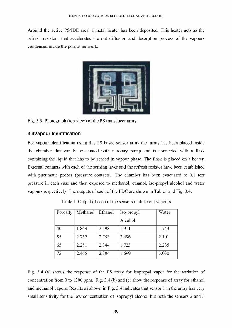
(Fig.3.1a, b, c). The output voltage of humidity sensors for different humidity is shown in Fig.
3.2.
3.3Principle of multiple vapour sensing
The sensitivity of PS capacitive sensors for different vapours depends significantly on the
pore dimensions and pore morphology of the porous structure as well as various physical
parameters of the vapours like molecular dimension, molecular weight, surface tension in the
liquid phase etc. [3]. This structure dependent sensitivity of PS sensor leads to the concept of
37
H.SAHA, POROUS SILICON SENSORS- ELUSIVE AND ERUDITE
PS-based vapour sensing array. In such an array, no individual detector responds solely to a
specific molecule, but the collective response of the entire array of detectors yields a unique
fingerprint for the vapour of interest [29]. Such arrays are often referred to as ‘electronic
nose’ and are not designated in advance to perform a specific task, but are instead developed
to identify and quantify vapours based on various signal-processing techniques [30]. This
approach to vapour sensing takes advantage of the collective output of an array of broadly
responsive detectors. We have studied on the selectivity and sensitivity of an array of four PS
sensors having different porosity for sensing of methanol, ethanol, iso-propyl alcohol and
water vapours. Matrix diagonalization method has been used for analysis of the vapours.[29].
Fig. 3.1: a) Schematic and actual photograph of PS Humidity Sensor with (b) single PS layer
and (c) four PS layers.
Fig 3.2: Response of porous silicon humidity sensor with the variation of humidity.
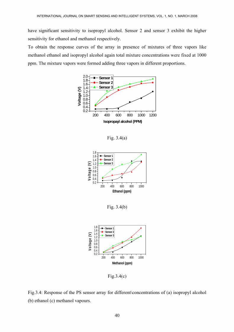
3.3.1 Fabrication of Sensor Array An array of four PS layers has been fabricated on an (100) oriented oxidized polished silicon
wafer having resistivity 1-2 Ωcm. The PS layers were formed by standard electrochemical
etching in HF based electrolyte through proper masking.. The porosity of different layers has
been varied in the range of 40%-75% by controlling the formation parameters and post
formation treatments [30].. Fig. 3.3 shows the top view of the actual PS transducer array.
38
INTERNATIONAL JOURNAL ON SMART SENSING AND INTELLIGENT SYSTEMS, VOL. 1, NO. 1, MARCH 2008
Around the active PS/IDE area, a metal heater has been deposited. This heater acts as the
refresh resistor that accelerates the out diffusion and desorption process of the vapours
condensed inside the porous network.
Fig. 3.3: Photograph (top view) of the PS transducer array.
3.4Vapour Identification
For vapour identification using this PS based sensor array the array has been placed inside
the chamber that can be evacuated with a rotary pump and is connected with a flask
containing the liquid that has to be sensed in vapour phase. The flask is placed on a heater.
External contacts with each of the sensing layer and the refresh resistor have been established
with pneumatic probes (pressure contacts). The chamber has been evacuated to 0.1 torr
pressure in each case and then exposed to methanol, ethanol, iso-propyl alcohol and water
vapours respectively. The outputs of each of the PDC are shown in Table1 and Fig. 3.4.
Table 1: Output of each of the sensors in different vapours
Porosity Methanol Ethanol Iso-propyl
Alcohol
Water
40 1.869 2.198 1.911 1.743
55 2.767 2.753 2.496 2.101
65 2.281 2.344 1.723 2.235
75 2.465 2.304 1.699 3.030
Fig. 3.4 (a) shows the response of the PS array for isopropyl vapor for the variation of
concentration from 0 to 1200 ppm. Fig. 3.4 (b) and (c) show the response of array for ethanol
and methanol vapors. Results as shown in Fig. 3.4 indicates that sensor 1 in the array has very
small sensitivity for the low concentration of isopropyl alcohol but both the sensors 2 and 3
39
H.SAHA, POROUS SILICON SENSORS- ELUSIVE AND ERUDITE
have significant sensitivity to isopropyl alcohol. Sensor 2 and sensor 3 exhibit the higher
sensitivity for ethanol and methanol respectively.
To obtain the response curves of the array in presence of mixtures of three vapors like
methanol ethanol and isopropyl alcohol again total mixture concentrations were fixed at 1000
ppm. The mixture vapors were formed adding three vapors in different proportions.
200 400 600 800 1000 12000.20.40.60.81.01.21.41.61.82.0
Sensor 1 Sensor 2 Sensor 3
Volta
ge (V
)
Isopropayl alcohol (PPM)
Fig. 3.4(a)
200 400 600 800 10000.20.40.60.81.01.21.41.61.8
Sensor 1 Sensor 2 Sensor 3
Vo
ltage
(V)
Ethanol (ppm)
Fig. 3.4(b)
200 400 600 800 10000.20.40.60.81.01.21.41.61.8 Sensor 1
Sensor 2 Sensor 3
Volta
ge (V
)
Methanol (ppm)
Fig.3.4(c)
Fig.3.4: Response of the PS sensor array for different\concentrations of (a) isopropyl alcohol
(b) ethanol (c) methanol vapours.
40
INTERNATIONAL JOURNAL ON SMART SENSING AND INTELLIGENT SYSTEMS, VOL. 1, NO. 1, MARCH 2008
Fig. 3.5 shows the dynamic response of the sensor 2 of the array for the mixture of the three
vapors.
0 500 1000 15000
0.5
1
1.5
2
2 .5
Tim e(S )
Vo
lta
ge
(V)
m = 300 ppme = 400 ppmi = 300 ppm
m = 400 ppm e = 300 ppm i = 300 ppm
m = 300 ppm e = 100 ppm i = 600 ppm
m = 100 ppm e = 300 ppm i = 600 ppm
Fig.3.5 dynamic response of here vapours
4.Gas sensors
Porous silicon has been used as gas sensors, particularly for a number of gases like
hydrogen,NO2, CO etc
Hydrogen detection by porous silicon has been reported in [31]. The basic principle of
operation of PS based hydrogen sensor is as follows:
Thin layer of Pd is deposited on the surface of the porous silicon layer consisting of silicon
islands. As Pd on top of the high impedance PS layer adsorbs hydrogen, its volume expands
bringing it in contact with neighboring Pd, dramatically reducing this impedance. The change
in impedance is correlated to hydrogen concentration. The large surface to volume ratio in Pd
nanoparticles in this sensor maximize the hydrogen adsorption area, while minimizing the
diffusion of hydrogen due to reduced thickness of the particles.This results in higher
sensitivity, faster response and shorter desorption times.
4.1 Hydrogen Sensor fabrication and Characterization[31].
The porous silicon layer was fabricated from a p-type (1 0 0) silicon wafer of low resistivity
(0.001–0.004 ohmcm) by etching at a current density of 25 mA/cm2 for an hour. Pd is
deposited by evaporation and annealed which oxidizes partly Pd to PdO. While the Pd
directly absorbs hydrogen, PdO gets reduced by hydrogen and may return to Pd and
contribute to the sensing of the hydrogen. Processes for the reduction of PdO to Pd takes
place at 1000C. The present sensor is operated at room temperature and the possibility of
room temperature conversion is small. The sensors baseline resistivity was measured to be
41
H.SAHA, POROUS SILICON SENSORS- ELUSIVE AND ERUDITE
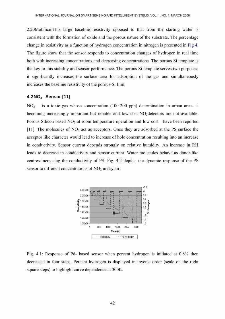
2.20MohmcmThis large baseline resistivity opposed to that from the starting wafer is
consistent with the formation of oxide and the porous nature of the substrate. The percentage
change in resistivity as a function of hydrogen concentration in nitrogen is presented in Fig 4.
The figure show that the sensor responds to concentration changes of hydrogen in real time
both with increasing concentrations and decreasing concentrations. The porous Si template is
the key to this stability and sensor performance. The porous Si template serves two purposes;
it significantly increases the surface area for adsorption of the gas and simultaneously
increases the baseline resistivity of the porous-Si film.
4.2 NO2 Sensor [11]
NO2 is a toxic gas whose concentration (100-200 ppb) determination in urban areas is
becoming increasingly important but reliable and low cost NO2detectors are not available.
Porous Silicon based NO2 at room temperature operation and low cost have been reported
[11]. The molecules of NO2 act as acceptors. Once they are adsorbed at the PS surface the
acceptor like character would lead to increase of hole concentration resulting into an increase
in conductivity. Sensor current depends strongly on relative humidity. An increase in RH
leads to decrease in conductivity and sensor current. Water molecules behave as donor-like
centres increasing the conductivity of PS. Fig. 4.2 depicts the dynamic response of the PS
sensor to different concentrations of NO2 in dry air.
Fig. 4.1: Response of Pd- based sensor when percent hydrogen is initiated at 0.8% then
decreased in four steps. Percent hydrogen is displayed in inverse order (scale on the right
square steps) to highlight curve dependence at 300K.
42
INTERNATIONAL JOURNAL ON SMART SENSING AND INTELLIGENT SYSTEMS, VOL. 1, NO. 1, MARCH 2008
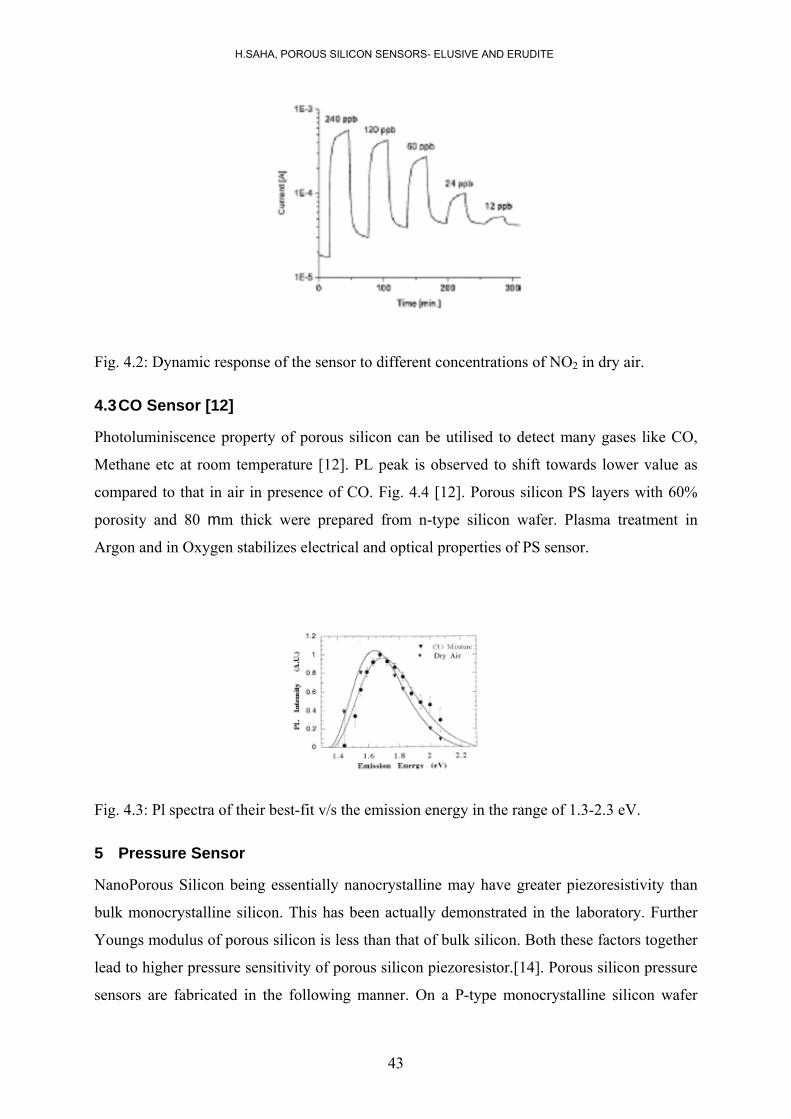
Fig. 4.2: Dynamic response of the sensor to different concentrations of NO2 in dry air.
4.3 CO Sensor [12]
Photoluminiscence property of porous silicon can be utilised to detect many gases like CO,
Methane etc at room temperature [12]. PL peak is observed to shift towards lower value as
compared to that in air in presence of CO. Fig. 4.4 [12]. Porous silicon PS layers with 60%
porosity and 80 mm thick were prepared from n-type silicon wafer. Plasma treatment in
Argon and in Oxygen stabilizes electrical and optical properties of PS sensor.
Fig. 4.3: Pl spectra of their best-fit v/s the emission energy in the range of 1.3-2.3 eV.
5 Pressure Sensor
NanoPorous Silicon being essentially nanocrystalline may have greater piezoresistivity than
bulk monocrystalline silicon. This has been actually demonstrated in the laboratory. Further
Youngs modulus of porous silicon is less than that of bulk silicon. Both these factors together
lead to higher pressure sensitivity of porous silicon piezoresistor.[14]. Porous silicon pressure
sensors are fabricated in the following manner. On a P-type monocrystalline silicon wafer
43
H.SAHA, POROUS SILICON SENSORS- ELUSIVE AND ERUDITE
(100) of resistivity 1-3 ohm-cm, oxidation is done in a dry-wet –dry sequence to form a thick
oxide (0.6 μm) layer. The sample is next micromachined by wet etchant at room temperature
to the desired thickness. This is followed by porous silicon formation by anodic etching
method in a two-pond cell. The area of the porous silicon layer is 2mm x 2mm.. Contacts on
top of porous silicon layer are formed by vacuum evaporation of aluminium and its
subsequent heat treatment at around 500°C for about 40-45 seconds. Contact area is 1mm x
1mm. The back contact metallisation is done by screen-printing of silver aluminium paste and
its subsequent firing at 700°C for 45 secs. The thickness of the porous silicon layer has been
restricted at 20μm on a p-type wafer since it has been found that on increasing the thickness
further, the porosity increases and fabrication of ohmic and stable metal contacts becomes
difficult. Thus the bulk silicon gives mechanical support to the structure. Also it provides the
desired porous silicon-silicon heterojunction needed for integrated temperature sensing and
compensation. Fig. 5.1 through Fig. 5.5 displays the pressure sensitivity of PS pressure
sensors.
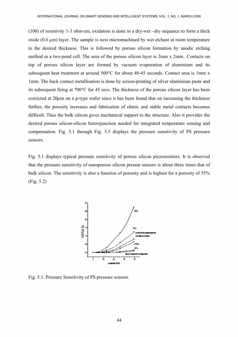
Fig. 5.1 displays typical pressure sensitivity of porous silicon piezoresistors. It is observed
that the pressure sensitivity of nanoporous silicon pressur sensors is about three times that of
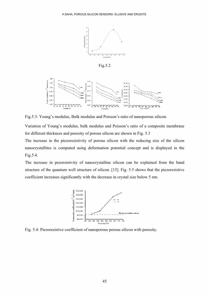
bulk silicon. The sensitivity is also a function of porosity and is highest for a porosity of 55%
(Fig. 5.2)
Fig. 5.1: Pressure Sensitivity of PS pressure sensors.
44
INTERNATIONAL JOURNAL ON SMART SENSING AND INTELLIGENT SYSTEMS, VOL. 1, NO. 1, MARCH 2008
35 40 45 50 55 60 65 70 75
0
5
10
15
20
25
30
Sen
sitiv
ity(m
V/V
/bar
)
porosity(%)
Fig.5.2
Fig.5.3: Young’s modulus, Bulk modulus and Poisson’s ratio of nanoporous silicon.
Variation of Young’s modulus, bulk modulus and Poisson’s ratio of a composite membrane
for different thickness and porosity of porous silicon are shown in Fig. 5.3
The increase in the piezoresistivity of porous silicon with the reducing size of the silicon
nanocrystallites is computed using deformation potential concept and is displayed in the
Fig.5.4.
The increase in pezorsistivity of nanocrystalline silicon can be explained from the band
structure of the quantum well structure of silicon. [15]. Fig. 5.5 shows that the piezoresistive
coefficient increases significantly with the decrease in crystal size below 5 nm.
Fig. 5.4: Piezoresistive coefficient of nanoporous porous silicon with porosity.
45
H.SAHA, POROUS SILICON SENSORS- ELUSIVE AND ERUDITE
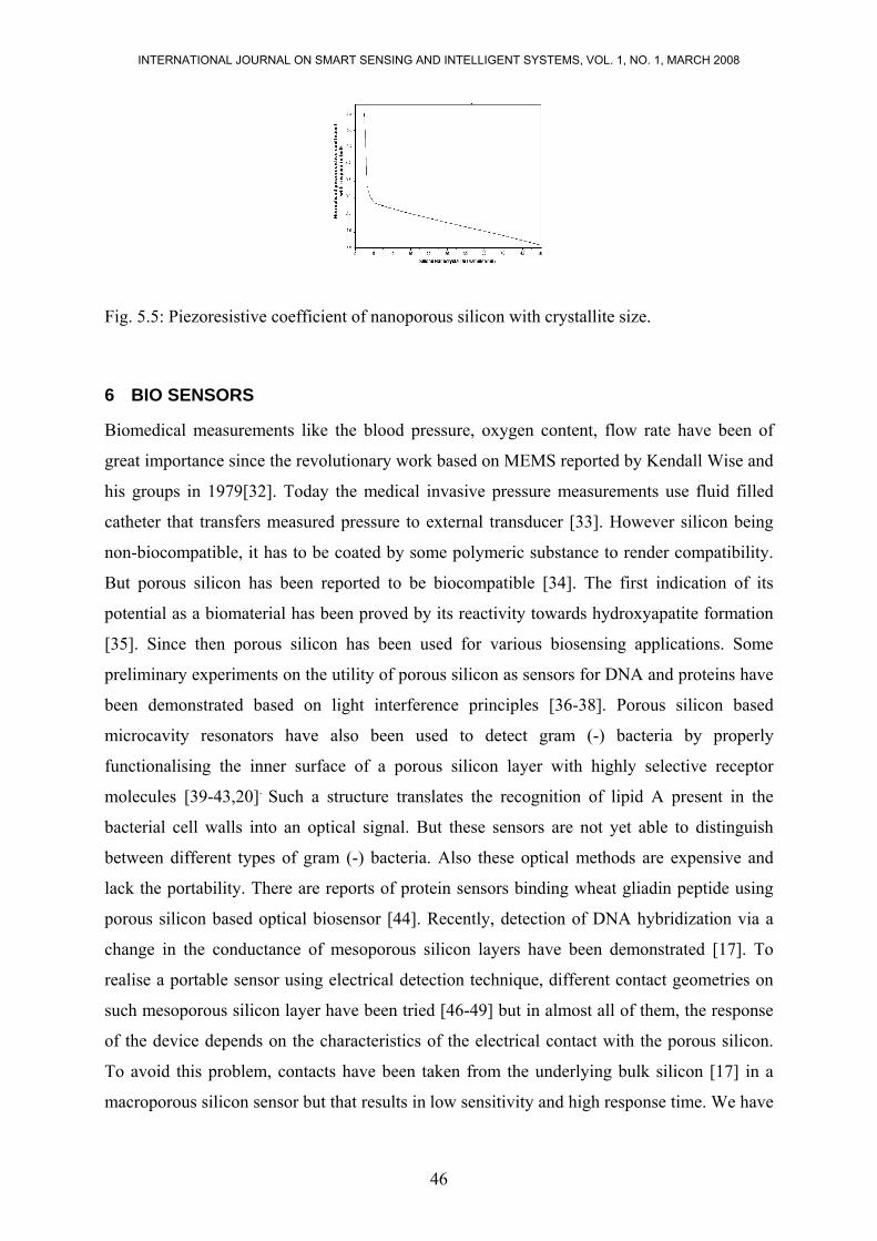
Fig. 5.5: Piezoresistive coefficient of nanoporous silicon with crystallite size.
6 BIO SENSORS
Biomedical measurements like the blood pressure, oxygen content, flow rate have been of
great importance since the revolutionary work based on MEMS reported by Kendall Wise and
his groups in 1979[32]. Today the medical invasive pressure measurements use fluid filled
catheter that transfers measured pressure to external transducer [33]. However silicon being
non-biocompatible, it has to be coated by some polymeric substance to render compatibility.
But porous silicon has been reported to be biocompatible [34]. The first indication of its
potential as a biomaterial has been proved by its reactivity towards hydroxyapatite formation
[35]. Since then porous silicon has been used for various biosensing applications. Some
preliminary experiments on the utility of porous silicon as sensors for DNA and proteins have
been demonstrated based on light interference principles [36-38]. Porous silicon based
microcavity resonators have also been used to detect gram (-) bacteria by properly
functionalising the inner surface of a porous silicon layer with highly selective receptor
molecules [39-43,20]. Such a structure translates the recognition of lipid A present in the
bacterial cell walls into an optical signal. But these sensors are not yet able to distinguish
between different types of gram (-) bacteria. Also these optical methods are expensive and
lack the portability. There are reports of protein sensors binding wheat gliadin peptide using
porous silicon based optical biosensor [44]. Recently, detection of DNA hybridization via a
change in the conductance of mesoporous silicon layers have been demonstrated [17]. To
realise a portable sensor using electrical detection technique, different contact geometries on
such mesoporous silicon layer have been tried [46-49] but in almost all of them, the response
of the device depends on the characteristics of the electrical contact with the porous silicon.
To avoid this problem, contacts have been taken from the underlying bulk silicon [17] in a
macroporous silicon sensor but that results in low sensitivity and high response time. We have
46
INTERNATIONAL JOURNAL ON SMART SENSING AND INTELLIGENT SYSTEMS, VOL. 1, NO. 1, MARCH 2008
reported the use of macroporous silicon as a platform for electrical sensing of biochemical
solutions where stable electrical contacts have been fabricated on porous silicon layer itself
after oxidation both by thermal method and by hydrogen peroxide. The reason for using
macroporous silicon as a platform is that it can be used to sense a wide variety of chemicals
ranging from polar to organic molecules. The value of the capacitance of the sensor is found
to be significantly large thus reducing the effects of parasitic capacitance in sensing. The
capacitance can also be changed considerably by tailoring the dimensions of the lateral
contacts on porous silicon layer. Macroporous silicon with such contact geometry also results
in a very high change in capacitance on exposure to solvents which facilitates the design of
the detection electronics. The solvents which have been used for sensing in this work are
different concentrations of glucose, potassium chloride and sodium chloride. The sensor has
been characterised in the presence of the biochemical solutions with both the different types
of oxides. The porous silicon layer with thermally grown oxide shows a significant difference
in response with solvents depending on their dielectric constant, dipole moment and
molecular dimension.
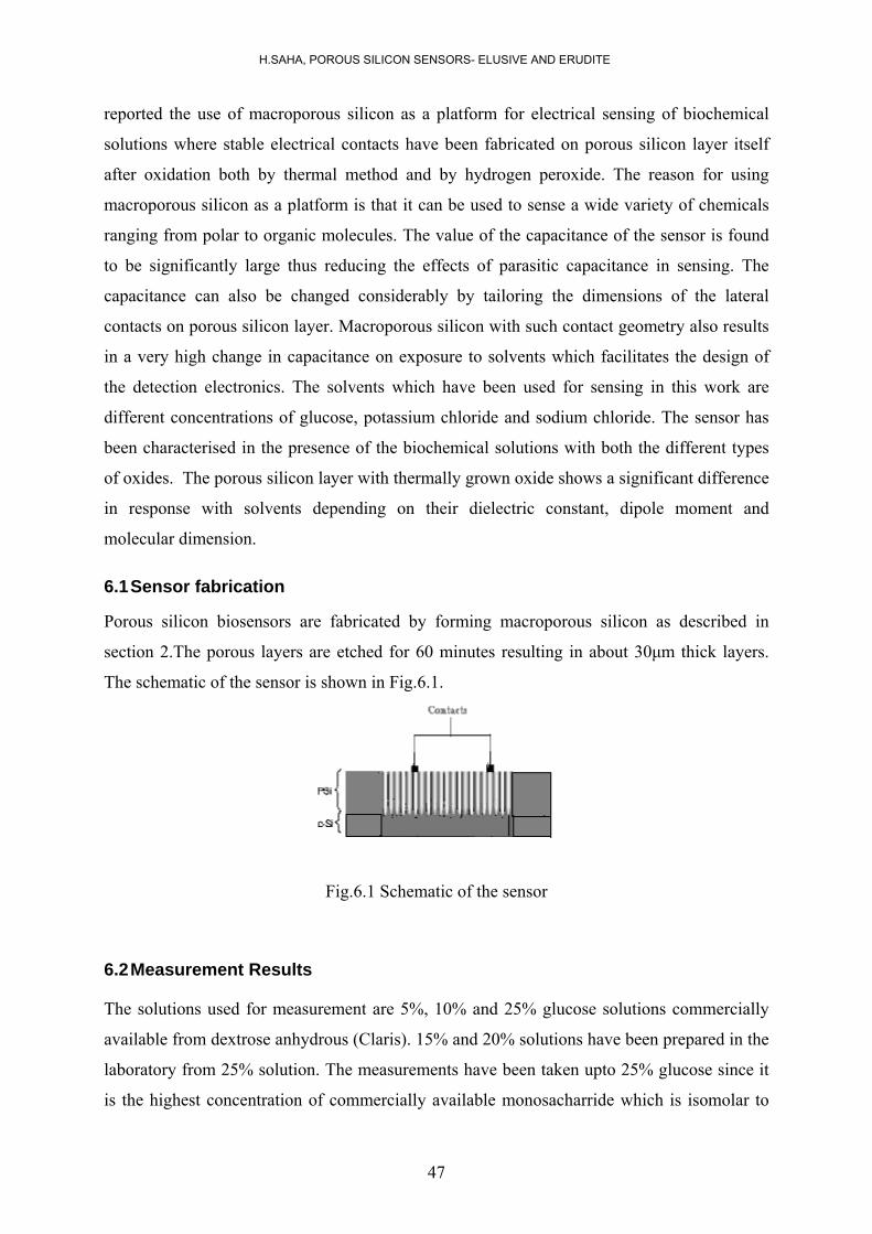
6.1 Sensor fabrication
Porous silicon biosensors are fabricated by forming macroporous silicon as described in
section 2.The porous layers are etched for 60 minutes resulting in about 30μm thick layers.
The schematic of the sensor is shown in Fig.6.1.
Fig.6.1 Schematic of the sensor
6.2 Measurement Results
The solutions used for measurement are 5%, 10% and 25% glucose solutions commercially
available from dextrose anhydrous (Claris). 15% and 20% solutions have been prepared in the
laboratory from 25% solution. The measurements have been taken upto 25% glucose since it
is the highest concentration of commercially available monosacharride which is isomolar to
47
H.SAHA, POROUS SILICON SENSORS- ELUSIVE AND ERUDITE
human plasma. Measurements have also been taken with potassium chloride solution
available in the form of Potchlor solution (Claris). Each ml of the solution contains 150mg of
potassium chloride. Five sets of solutions have been prepared by dilution with deionise water
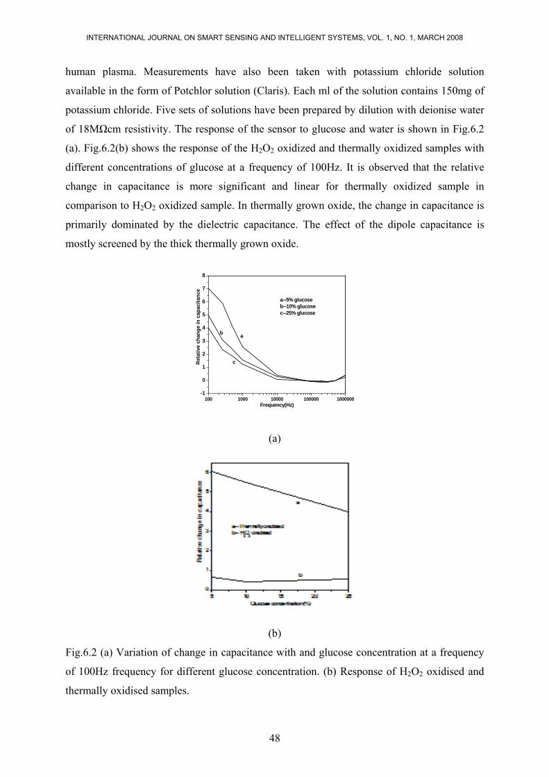
of 18MΩcm resistivity. The response of the sensor to glucose and water is shown in Fig.6.2
(a). Fig.6.2(b) shows the response of the H2O2 oxidized and thermally oxidized samples with
different concentrations of glucose at a frequency of 100Hz. It is observed that the relative
change in capacitance is more significant and linear for thermally oxidized sample in
comparison to H2O2 oxidized sample. In thermally grown oxide, the change in capacitance is
primarily dominated by the dielectric capacitance. The effect of the dipole capacitance is
mostly screened by the thick thermally grown oxide.
100 1000 10000 100000 1000000-1
0
1
2
3
4
5
6
7
8
a--5% glucoseb--10% glucose c--25% glucose
c
b a
Rel
ativ
e ch
ange
in c
apac
itanc
e
Frequency(Hz)
(a)
(b)
Fig.6.2 (a) Variation of change in capacitance with and glucose concentration at a frequency
of 100Hz frequency for different glucose concentration. (b) Response of H2O2 oxidised and
thermally oxidised samples.
48
INTERNATIONAL JOURNAL ON SMART SENSING AND INTELLIGENT SYSTEMS, VOL. 1, NO. 1, MARCH 2008
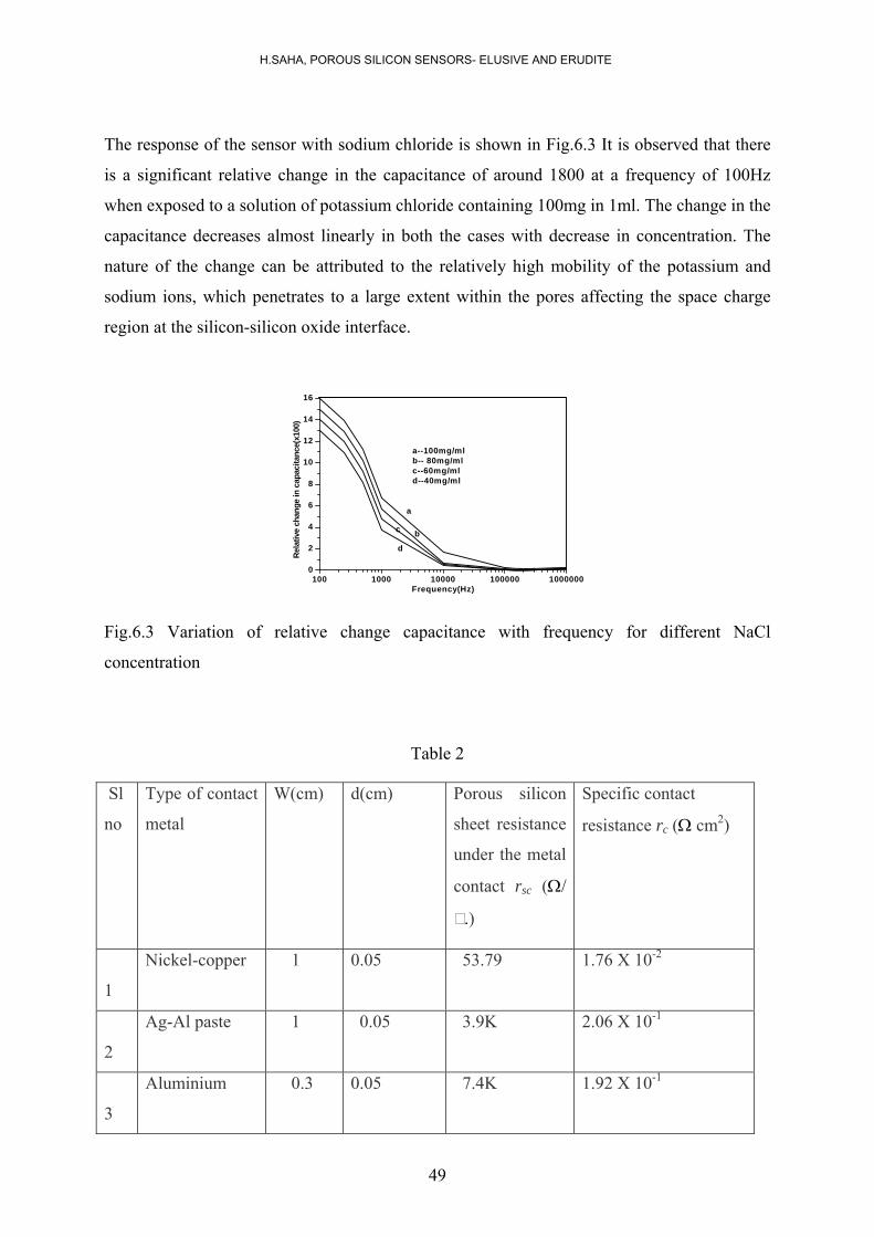
The response of the sensor with sodium chloride is shown in Fig.6.3 It is observed that there
is a significant relative change in the capacitance of around 1800 at a frequency of 100Hz
when exposed to a solution of potassium chloride containing 100mg in 1ml. The change in the
capacitance decreases almost linearly in both the cases with decrease in concentration. The
nature of the change can be attributed to the relatively high mobility of the potassium and
sodium ions, which penetrates to a large extent within the pores affecting the space charge
region at the silicon-silicon oxide interface.
100 1000 10000 100000 10000000
2
4
6
8
10
12
14
16
a--100mg/mlb-- 80mg/mlc--60mg/mld--40mg/ml
d
c b
a
Rela
tive
chan
ge in
cap
acita
nce(
x100
)
Frequency(Hz)
Fig.6.3 Variation of relative change capacitance with frequency for different NaCl
concentration
Table 2
Sl
no
Type of contact
metal
W(cm) d(cm) Porous silicon
sheet resistance
under the metal
contact rsc (Ω/
.)
Specific contact
resistance rc (Ω cm2)
1
Nickel-copper 1 0.05 53.79 1.76 X 10⁻²
2
Ag-Al paste 1 0.05 3.9K 2.06 X 10⁻¹
3
Aluminium 0.3 0.05 7.4K 1.92 X 10⁻¹
49
H.SAHA, POROUS SILICON SENSORS- ELUSIVE AND ERUDITE
6.3 Challenges of PS sensor
It is to be noted that no commercial sensors based on porous silicon have been developed so
far due to the lack of its stability and reproducibility. This is mainly because of the
uncontrolled growth of pores on the silicon surface. Intensive research on ordered porous
silicon formation by template transfer technology is required to apply the immense sensing
potential of porous silicon commercial purposes.
(a) Contact: Making ohmic contact to any semiconductor is in general not so easy but for PS
it is really a challenging task. The high resistivity ( tens of kilo-ohms to tens of mega-ohms),
presence of SiO at the surface, doping difficulty , micropore to nanopore distribution and
localised nonuniformity – all join together to realise ohmic contact on PS a real problem.
Vacuum evaporation or sputtering of suitable metals followed by short heat treatments have
not been always successful although most commonly practiced. Metal plating by
electrochemical or electroless techniques need to be further improved. The problem is much
more serious for p PS. Most commonly contact is formed on PS layer by evaporating
Aluminium and then annealing it subsequently. However Al contact usually is not ohmic in
nature and displays rectifying characteristics. Further it undergoes ageing when exposed to
atmosphere for a prolonged time.
2
+
Low resistance contacts on porous silicon have been
realized by electroless nickel deposition from a very weakly alkaline solution followed by
copper thickening. Nickel is deposited over porous silicon by electroless deposition
technique. 0.0038 M nickel sulphate solution is mixed with 0.242M ammonium fluoride
solution at room temperature and PH adjusted to 7.5 Copper has been deposited over the
nickel layer by electrochemical plating process to increase the metal layer thickness and to
decrease the sheet resistance further. The specific contact resistance as measured by the above
mentioned technique for three different metals like nickel, Ag-Al paste, aluminium with
porous silicon is given in Table1.It is observed that the specific contact resistance for Nickel –
copper plated porous silicon is better in comparison with other two. Similar values of contact
resistance of silver on p-type silicon has been reported in [19]. Also on comparing the contact
resistance of nickel on porous silicon with gold reported in [20] shows that contact resistance
of nickel is around 10ohm while that of gold is around 20-100ohm.A low value of the sheet
resistance for nickel compared to other metals is perhaps due to the formation of nickel
silicide with porous silicon.
50
INTERNATIONAL JOURNAL ON SMART SENSING AND INTELLIGENT SYSTEMS, VOL. 1, NO. 1, MARCH 2008
(b) High Resistivity: Porous Silicon is an effective media of Silicon, SiO and void. The pore
size and pore distribution and morphology as well as the volume fraction of Si/SiO greatly
affects the resistivity of PS. Besides a large number of traps and recombination centres are
present at the Si/SiO interfaces which capture the mobile carriers and increase the resistivity
of PS very significantly. This is particularly important in p+ PS where a p+ Si attains a very
high resistivity(>100 megohm-cm) after PS anodisation although the porosity is rather low (<
30%) . The probable quantum confinement of carriers in high porosity PS may contribute to
its increased resistivity. Exposure to ambient and subsequent oxidation of Si changing the
Si/SiO volume fraction enhances the resistivity further. Metal, organic materials or
polysilicon capping have been tried to prevent the oxidation caused by ambient exposure
surface.
2
2
2
2
(c) Non-uniformity: It is well known that PS suffers from both vertical and lateral non-
uniformity during its formation. This would lead to non-uniform distribution of resistivity,
dielectric constant, refractive index and photoluminescence properties of PS which is
undesirable for device functioning. Efforts to improve uniformity both vertical and lateral
have been made by controlling the formation parameters and techniques but much more need
to be done in this regard. Use of Alumina templates formed by depositing thin film of Al on
silicon and then anodizing Al to form an ordered structure of Alumina may be tried for
regular and ordered structure of PS. For removing vertical non-uniformity pore branching
during formation of PS layer is to be avoided. Use of DMF based electrolyte solution during
PS formation leads to vertical pores without pore branching. However the pore morphology is
affected by the change of the composition of electrolyte, which needs to be optimisd for the
purpose.
(d) Doping Difficulty: Doping of PS by thermal diffusion or ion implantation is rather
difficult and very little work has been carried out in this regard. The presence of very high
surface state density at Si/SiO2 interface, passivation of nano or micro-structured Silicon
skeletons cause diffusion of desirable dopants rather difficult. Surface passivation of the pore
walls by hydrogen treatment at high temperature are reported to lead to considerable
reduction in surface state densities.
(e) Instability: One of the principal limitations of PS is its high surface activity leading to
adsorption of moisture, oxygen and other contaminants in the ambient which subsequently
change the composition of PS and cause its “aging”. Lot of work has been done to prevent or
51
H.SAHA, POROUS SILICON SENSORS- ELUSIVE AND ERUDITE
minimise aging of PS including capping of PS with metals, organic polymers and polysilicon.
Oxidising PS intentionally right in the beginning is another approach for improving its
stability. Oxidising of PS can be done by thermal oxidation, or by H O treatment, or by
anodic oxidation. 2 2
(f) Local formation and patterning of PS: For device fabrication it is essential to form
locally porous silicon layers on a silicon substrate to a predefined pattern. This can be
achieved in a number of ways: (a) by local anodisation of patterned crystalline Si surfaces
through a mask, (b) selective anodisation using etch stops and (c) by patterning uniform PS
through photolithographic and etching techniques. Lot of work needs to be done in this area.
Attempts are being made to realize wheatstone bridge structure of PS piezoresistors for
fabrication of a PS pressure sensor by lithographic technique.
(g) Freestanding Porous Silicon: Most of the PS devices are fabricated on PS/Si
heterojunction but sometimes it is essential to have a freestanding PS layer. However the
fabrication of freestanding PS and pasting on a suitable substrate with front and back contacts
is still in aninfantile state. Freestanding PS layer has been fabricated in connection with solar
cell fabrication but its use as sensors is yet to be explored.
7 Conclusions
Porous Silicon is an excellent platform for various types of sensors. Humidity sensors,
Vapour sensors,Gas sensors,Pressure sensors and also BioSensors have been fabricated and
tested in the laboratories. All of them have displayed very high sensitivity, room or relatively
low temperature operation, desirable selectivity and also fast response time as compared to
their conventional counterparts. Moreover porous silicon sensors are compatible to silicon IC
technology. However their largescale commercial use has been prevented due to a number of
limitations. These limitations are not fundamental but need to be overcome through ingenous
engineering. Intensive research is called for this purpose.
8 REFERENCES
1] H. Saha, S. Dey, C. Pramanik, J. Das and T. Islam, Porous Silicon-Based Smart Sensors,
Encyclopedia of Sensors, ed. C.A. Grimes, E.C. Dickey and M.V. Pisako, Vol.8, pages
163-196, 2006. Americal Scientific Publishers.
2] C. Baratto, G. Faglia, G. Sberveglieri, Z. Galurro, L. Panchesi, C. Olon and L. Pavesi,
Sensors 2, 121 (2002).
52
INTERNATIONAL JOURNAL ON SMART SENSING AND INTELLIGENT SYSTEMS, VOL. 1, NO. 1, MARCH 2008
3] H. Saha, J. Das and S.M. Hossain, Asian J. Physics, 12 (283), 323 (2003).
4] T. Taliercio et.al. Sensors Actuators A, 46-47, 43 (1995).
5] T. Das, S. Dey, S.M. Hossain, Z.M. Rittersme and H. Saha, IEEE Sensors, Journal 3(4),
414 (2004).
6] J. Das, S.M. Hossain, S. Chakraborty and H. Saha, Sensors and Actuators, A 94, 44
(2001).
7] Z. M. Rittersme, Humidity Sensors – Review, Sensors and Actuators.
8] S. J. Kim, S. H. Lee, C. J. Lee, organic vapour sensing by current response of porous
silicon layer, J. Phys. D., Appl. Phys. 34, (2002), 3505-3509.
9] K. Watanabe, T. Okada, L. Choe, Y. Sato, organic vapour sensitivity in a porous silicon
device, Sensors and Actuators B, 33 (1996), 194-197.
10] A. Motohashi, M. Rinike, M. Kawakami, H. Aoyagi, A. Kinoshita, A. Saton,
Identification of water molecules in low humidity and possibility of quantitative gas
analysis using porous silicon gas sensor, Jpn. J. Appl. Phys. Part-I, 35 (1996) 4253-56.
11] L. Pavesi, PS NO2 has sensors, sensors & Actuators A.
12] C. Baratto, E. Comini, G. Faglia, G. Sberveglieri, G. Di Francia, F.De Filippo, V. La
Ferrara, L. Quercia, L. Lanullotti, Gas Detection with a porous silicon based sensors,
Sensors and Actuators B, Vol. 65, 2000, pp. 257-259.
13] T.E. Bell, P.T. Genissen, D. DeMunter and M. Kuhl, Porous Silicon as a Sacrificial
Material, J. Micromech. Microeng, Vol. 6, pp. 361-369, 1996.
14] C. Pramanik and H. Saha, Piezoresistive Pressure sensing by Porous Silicon Membrane,
IEEE Sensors Journal, Vol. 6, No.2, April 2006, pp. 301-309.
15] C. Pramanik, S. Banerjee, H. Saha and C.K. Sarkar “Piezoresistivity of Silicon Quantum
well wire” – Nanotechnology, 17, (2006) 3209-3214.
16] C.A. Betty, R. Lal, D.K. Sharma, J. V. Yakhimi, J. P. Mittal, Macroporous Silicon based
Capacitive affinity sensor – fabrication and electrochemical studies, sensors and
actuators B 97 (2004), pp. 334-343.
17] M. Archer, M. Christophersen, P. M. Fauchet, Electrical Porous Silicon Chemical
sensor for detection of organic solvents, sensors and actuators, B 106 (2005) 347-357.
18] Finny P. Mathew and Evangelyn C. Alocilja, Fabrication of Porous Silicon Based
Biosensors, ‘0-780 3-8133-5/03/$ 15.00 2003 IEEE.
19] Porous Silicon based biosensor for pathogenor detection, Biosensor Bioelectronics, Vol.
20 (8), pp. 1656-61 (2005).
53
H.SAHA, POROUS SILICON SENSORS- ELUSIVE AND ERUDITE
20] Lisa A. Delonise and Benjamin L. Miller, Quantitative Assessment of Enzyme
Immobilisation capacity in porous silicon, Analytical chemistry A-H, 2004.
21] M. Archer and PM Fanchet, Electrical Sensing of DNA hybridization in porous silicon
layers, Phys. Status Solidi a 198, 503-7.
22] ISAMA – IIT Kgp paper on contact.
23] R. J. Martin – Palna, J. Perez – Rigueiro, R. Guerrero – Lemus, J.D. Moreno and J. M.
Martinez – Duart, Aging of aluminium electrical contacts to porous silicon, J. Appl.
Phys. 85, January (1991), 583-586.
24] J. Kanungo, C. Pramanik. S. Bandopadhyay, U. Gangopadhyay, L. Das, H. Saha and
Rober TT Gettens, Improved contacts on a porous silicon layer by electroless nickel
plating and copper thicknessing, semiconductor Science and Technology, 21, (2006)
964-970.
25] S. Dhar and S. Chakraborti, Electroless Nickel Matel contacts on porous silicon App;.
Phys, Letter 68, 1392-3.
26] F.A. Harraz, T. Sukka and Y Holga, Immersion plating of nickel onto a porous silicon
layer from fluoride solutions physics status solidi a 197 p. 51-56 (2003).
27] S. M. Hossain, S. Chakraborty, S. K. Dutta, J. Das and H. Saha, J. Luminescence, 91,
195 (2000).
28] B. Gellowz, T. Nakagawn and N. Koshide, Enhancement of the quantum efficiency and
suitability of electroluminescence from porous silicon by anodic passivation, B. Gelloz,
T. Makagawa and N. Koshide, Appl. Phys. Letts., 73 (1998) pp 2021-2023.
29] Tarikul Islam, PhD thesis, Developmentof Porous Silicon Based Humidity Sensor and
Organic Vapor Sensor Array with Integrated Signal Processing Systems,2007, Jadavpur
University
30] T.Islam,J.Das,H.Saha,Porous silicon based organic vapour sensors array
for e-nose applications,5th IEEE Senor Conf, Oct 22-25,2006,Daegue,Korea
31] K.Luong,A.Sine,S.Bhansali,Devlopmen of a highl sensitive poroussi-based hydrogen
snsor using Pd nanostructures, Sensors and Actuators, B,111-112(2005),125-129
32] J.M.Borky, K.D.Wise, Integrated Signal Conditioning for Silicon Pressure Sensors, IEEE
Transactions on Electron Devices, vol.ED-26, no.12,p.1906(1979).
54
INTERNATIONAL JOURNAL ON SMART SENSING AND INTELLIGENT SYSTEMS, VOL. 1, NO. 1, MARCH 2008
33] A. Druzhinin, E. Lavitska, I. Maryamova, "Medical pressure sensors on the basis of
silicon microcrystals and SOI layers", Sensors and Actuators B, vol. 58,pp. 415-
419,1999.
34]. Properties of porous silicon, ed Canham L.T.INSPEC: The institution of Electrical En
gineers, London, UK, 1997.
35] Lorraine Buckberry, Sue Bayliss, Materials World, vol.7, no.4, pp.213-15,1999.
36] Chan S.,fauchet P.M., Li Y.,Rothberg L.J., Proc.SPIE, vol.23,p.3912,2000.37] Janshoff
A., Dancil K.P..S.,Steinem C.,Greiner D.P., Lin V.S.Y., Gurtner C., Motesharei K., Sailor
M.J., Ghadiri M.R., J. Am Chem Soc.,vol.120, p.12108, 1998.
38]. Lin V.S.Y.,Motesherai K.,Dancil K.P.S., Sailor M.J., Ghadiri M.R., Science, vol.278,
p.840,1997.
39] Selena Chen, Scott R.Horner,P.M.Fauchet, B.Miller, “Identification of gram negative
bacteria using Nanoscale silicon microcavities”, J. Am. Chem Soc., vol.133,pp.11797-
11798,2001.
40] DeLouise, L. A.; Miller, B. L. Proc. SPIE 2004, 5357, 111-125.
41] DeLouise, L. A.;P.M.Fauchet, Miller, B. L, Alice Pentland, “Hydrogel supported optical
microcavity sensors”, Advanced Materials, vol.17, pp.2199-2203(2005).
42] Lisa A. DeLouise, Peng Meng Kou, and Benjamin L. Miller, “Cross-Correlation of
Optical Microcavity Biosensor Response with Immobilized Enzyme Activity.Insights into
Biosensor Sensitivity”, Analytical Chemistry A-H, 2005
43]. Lisa A. DeLouise and Benjamin L. Miller, “Enzyme Immobilization in Porous
Silicon:Quantitative Analysis of the Kinetic Parameters for Glutathione-S-transferases”,
Anal. Chem.2005, 77,1950-1956.
44] Mathew FP, Alocilja EC, “Porous silicon based biosensor for pathogen detection”,
Biosensor Bioelectronics, vol.20(8),pp.1656-61(2005).
45].L.D.Stefano, M.Rossi, M.Staiano, G.Mamone, A.Parracino, L.Rotiroti, I.Rendina,
M.Rossi, S.D.Auria, “Glutamine Binding Protein from Escherichia coli specifically binds
a wheat gliadin peptide allowing the deisgn of a new porous silicon based optical
biosensor”, J. of Americal Chemical Society, available online from March 2006.
46].A.Motohashi, M.Ruike, M.Kawakami, H.Aoyagi, A.Kinoshita, A.Satou, “Identification of
water molecules in low humidity and possibility of quantitative gas analysis using porous
silicon gas sensor”, Jpn. J. Appl. Phys.,1996, p.4253
55
H.SAHA, POROUS SILICON SENSORS- ELUSIVE AND ERUDITE

47]. A.Motohashi, M.Kawakami, H.Aoyagi, A.Kinoshita, A.Satou, “Gas identification by a
single gas sensor using porous silicon as the sensitive material”, Jpn. J. Appl. Phys.,1995,
p.5840
48] K.Watanabe, T.Okada, I.Choe, Y.Sato, “Organic vapour sensitivity in a porous silicon
device”, Sens. Actuat. B, 1996, p.194
49] S.J.Kim, S.H.Lee,C.J.Lee, “Organic vapour sensing by current response of porous silicon
layer”, J.Phys.D: Appl. Phys., 2002, p.3505.
56
INTERNATIONAL JOURNAL ON SMART SENSING AND INTELLIGENT SYSTEMS, VOL. 1, NO. 1, MARCH 2008