portable and foldable magnetic loop antenna - yo3ggx
TRANSCRIPT

IOSR Journal of Electronics and Communication Engineering (IOSR-JECE)
e-ISSN: 2278-2834,p- ISSN: 2278-8735. Volume 6, Issue 5 (Jul. - Aug. 2013), PP 01-11 www.iosrjournals.org
www.iosrjournals.org 1 | Page
Design, Validation and Correlation of Characterized SODIMM
Modules Supporting DDR3 Memory Interface
Vemula Harini, Sandiri Rajendar
(Department of ECE, Vardhaman College of Engineering, Hyderabad, A.P, India)
Abstract : In any computing environment, it is necessary for the processor to have fast accessible RAM that
allows temporary storage of data. DDR3- SODIMM module is a key component in the memory interface and is
becoming increasingly important in enabling higher speeds. Considering higher bandwidths and speeds more
than 1GHz, DDR3 is enabling poses more and more high speed signaling and design challenges. Characterized
SODIMM module need to be designed to understand and analyze the impact of SODIMM parameters at higher
speeds and thereby define more robust memory interface. This will include simulation, board design, validation
and results correlation and involves high speed simulation and validation methodologies.
Keywords – Validation, Correlation, DDR3, Characterized SODIMM, Signal Integrity.
I. Introduction
In this paper we are discussing about the design, validation and correlation of Characterized SODIMM
module supporting DDR3 memory interface.
1.1 To define SODIMM variables more accurately Based on simulations, SODIMM variables are one of the top contributors towards memory SI (Signal
Integrity) parameters. Usually for those SODIMM variables (Z, RLC, buffer characteristics, ODT values etc), a
fixed number is accounted in timing and spreadsheets while calculating overall system margin. Lab data from
Skewed SODIMM based on Skewed SDRAM, should give us more insight into most of these parameters; its
value and how much they vary across devices. Effort will be to quantify each of these parameters and its impact;
try to understand which parameter is prominent in determining SI. At higher speeds , this effort should make
timing allocations more meaningful.
1.2 For better Correlation between Simulation data and Lab data If there is a deviation, it will enable further analysis and optimization of simulation methodology. To
optimize the SDRAM simulation models. More data available for vendor specific high density raw cards and
how well they correlate with JEDEC specs. End goal is to have more accurate simulation models.
1.3 Try to hit worse case corner in DDR3 Electrical Validation (EV) As of now most of the SODIMM available for EV are typical corner. As speeds are getting higher and
margins are shrinking, this may help us to cover worst case corners.
1.4 Better probing solutions for high density Raw Cards With bigger packages and higher density its tough to probe a signal on SODIMM (Close to the ball).
This leads to analysis of distorted waveforms .Skewed SODIMM will have test points for better data collection.
The rest of this paper is organized as follows Section 2 describing about the memory interface and related work . Section 3 presents the SODIMM design part. Section 4 gives the lab measured data. Section 5 verifies the
results using simulation. Section 6 gives the correlation of lab data with simulated data. The paper concludes
with Section 7.
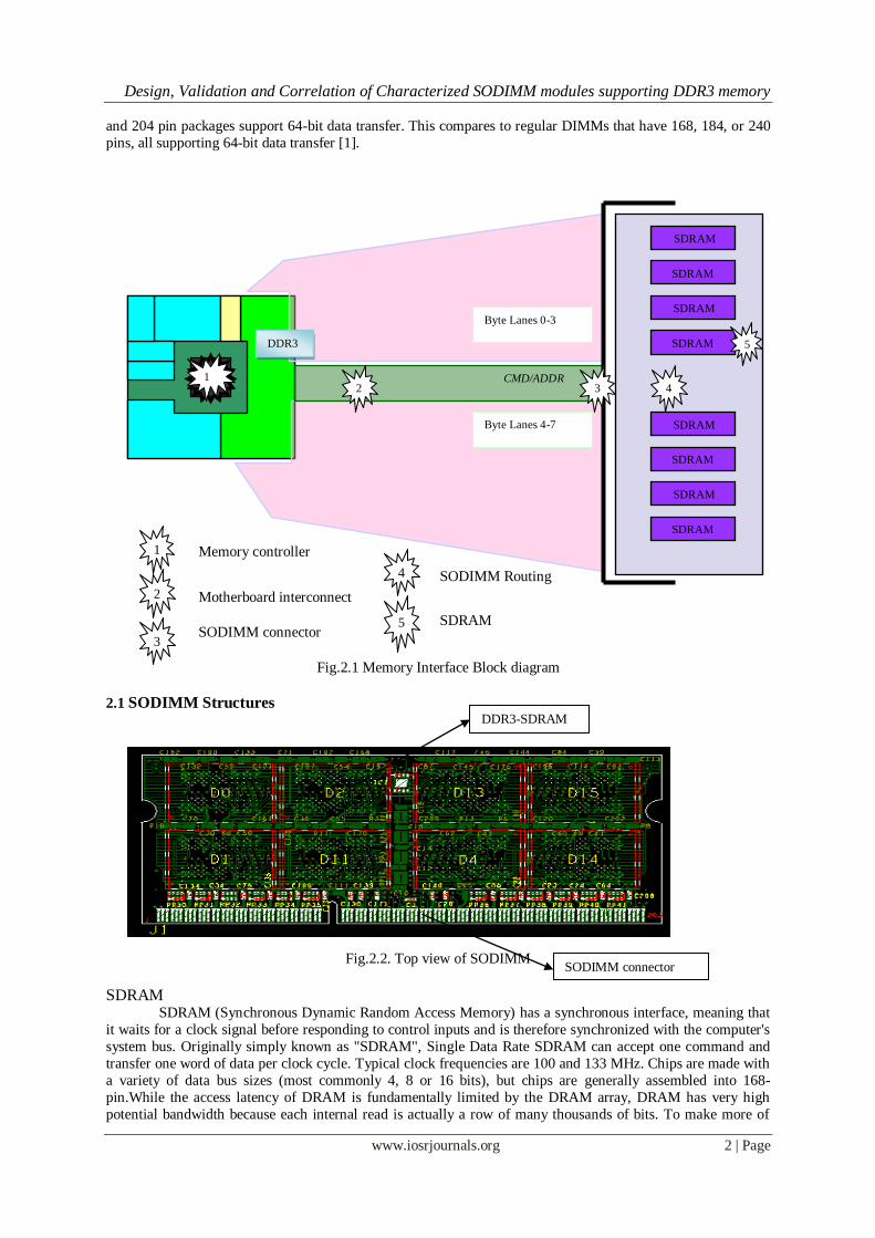
II. Memory Interface Let’s examine in detail, each component in the memory interface. The memory interface diagram is as
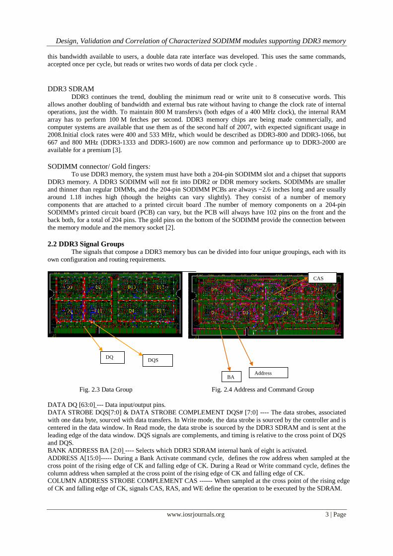
shown in the Fig.2.1.A SO-DIMM, or small outline dual in-line memory module, is a type of computer memory
built using integrated circuits. SO-DIMMs have 72, 100, 144, 200 or 204 pins. The top view of the SODIMM
structure is shown in the Fig.2.2. The 72 and 100 pin packages supports 32-bit data transfer, while the 144, 200
Submitted Date 19 June 2013 Accepted Date: 24 June 2013
Design, Validation and Correlation of Characterized SODIMM modules supporting DDR3 memory
www.iosrjournals.org 2 | Page
and 204 pin packages support 64-bit data transfer. This compares to regular DIMMs that have 168, 184, or 240
pins, all supporting 64-bit data transfer [1].
Fig.2.1 Memory Interface Block diagram
2.1 SODIMM Structures
Fig.2.2. Top view of SODIMM
SDRAM SDRAM (Synchronous Dynamic Random Access Memory) has a synchronous interface, meaning that
it waits for a clock signal before responding to control inputs and is therefore synchronized with the computer's
system bus. Originally simply known as "SDRAM", Single Data Rate SDRAM can accept one command and
transfer one word of data per clock cycle. Typical clock frequencies are 100 and 133 MHz. Chips are made with
a variety of data bus sizes (most commonly 4, 8 or 16 bits), but chips are generally assembled into 168-
pin.While the access latency of DRAM is fundamentally limited by the DRAM array, DRAM has very high
potential bandwidth because each internal read is actually a row of many thousands of bits. To make more of
DDR3-SDRAM
SODIMM connector
Motherboard interconnect 2
Memory controller 1
3 SODIMM connector
SODIMM Routing
SDRAM
4
5
1
SDRAM
SDRAM
CMD/ADDR
SDRAM
SDRAM
SDRAM
SDRAM
SDRAM
SDRAM
Byte Lanes 0-3
Byte Lanes 4-7
2 3 4
5
1
DDR3
Design, Validation and Correlation of Characterized SODIMM modules supporting DDR3 memory
www.iosrjournals.org 3 | Page
this bandwidth available to users, a double data rate interface was developed. This uses the same commands,
accepted once per cycle, but reads or writes two words of data per clock cycle .
DDR3 SDRAM DDR3 continues the trend, doubling the minimum read or write unit to 8 consecutive words. This
allows another doubling of bandwidth and external bus rate without having to change the clock rate of internal operations, just the width. To maintain 800 M transfers/s (both edges of a 400 MHz clock), the internal RAM
array has to perform 100 M fetches per second. DDR3 memory chips are being made commercially, and
computer systems are available that use them as of the second half of 2007, with expected significant usage in
2008.Initial clock rates were 400 and 533 MHz, which would be described as DDR3-800 and DDR3-1066, but
667 and 800 MHz (DDR3-1333 and DDR3-1600) are now common and performance up to DDR3-2000 are
available for a premium [3].
SODIMM connector/ Gold fingers:
To use DDR3 memory, the system must have both a 204-pin SODIMM slot and a chipset that supports
DDR3 memory. A DDR3 SODIMM will not fit into DDR2 or DDR memory sockets. SODIMMs are smaller
and thinner than regular DIMMs, and the 204-pin SODIMM PCBs are always ~2.6 inches long and are usually
around 1.18 inches high (though the heights can vary slightly). They consist of a number of memory
components that are attached to a printed circuit board .The number of memory components on a 204-pin
SODIMM's printed circuit board (PCB) can vary, but the PCB will always have 102 pins on the front and the
back both, for a total of 204 pins. The gold pins on the bottom of the SODIMM provide the connection between
the memory module and the memory socket [2].
2.2 DDR3 Signal Groups The signals that compose a DDR3 memory bus can be divided into four unique groupings, each with its
own configuration and routing requirements.
Fig. 2.3 Data Group Fig. 2.4 Address and Command Group
DATA DQ [63:0] --- Data input/output pins.
DATA STROBE DQS[7:0] & DATA STROBE COMPLEMENT DQS# [7:0] ---- The data strobes, associated
with one data byte, sourced with data transfers. In Write mode, the data strobe is sourced by the controller and is
centered in the data window. In Read mode, the data strobe is sourced by the DDR3 SDRAM and is sent at the
leading edge of the data window. DQS signals are complements, and timing is relative to the cross point of DQS
and DQS.
BANK ADDRESS BA [2:0] ---- Selects which DDR3 SDRAM internal bank of eight is activated.
ADDRESS A[15:0]----- During a Bank Activate command cycle, defines the row address when sampled at the
cross point of the rising edge of CK and falling edge of CK. During a Read or Write command cycle, defines the
column address when sampled at the cross point of the rising edge of CK and falling edge of CK. COLUMN ADDRESS STROBE COMPLEMENT CAS ------ When sampled at the cross point of the rising edge
of CK and falling edge of CK, signals CAS, RAS, and WE define the operation to be executed by the SDRAM.
DQS DQ
BA Address
CAS

Design, Validation and Correlation of Characterized SODIMM modules supporting DDR3 memory
www.iosrjournals.org 4 | Page
Fig. 2.5 Control Group Fig. 2.6 Clock Group
CHIP SELECT COMPLEMENT CS# [1:0] ------ Enables the associated DDR3 SDRAM command decoder
when low and disables the command decoder when high. When the command decoder is disabled, new commands are ignored but previous operations continue. Rank 0 is selected by S0; Rank 1 is selected by S1.
CLOCK ENABLE CKE [1:0] ------ Activates the DDR3 SDRAM CK signal when high and deactivates the CK
signal when low. By deactivating the clocks, CKE low initiates the Power Down mode or the Self Refresh
mode.
Clock and Clock complement CK0/CK0#, CK1/CK1# ------- The system clock inputs. All address and
command lines are sampled on the cross point of the rising edge of CK and falling edge of CK. A Delay Locked
Loop (DLL) circuit is driven from the clock inputs and output timing for read operations is synchronized to the
input clock [3].
III. SODIMM Design Board design has become more complex as device pin density and system frequency increase. A
successful high-speed board must effectively integrate devices and other elements while avoiding signal
transmission problems associated with high-speed I/O standards. Board design process is same as the
conventional design process only but it uses the different stack up details. The stack up details will discussed as
follows. The DDR3 SO-DIMM printed circuit board design uses multi-layers of glass epoxy material.The
reference planes can be divided so adjacent signal layers maintain a constant Vss or Vdd reference. All data is
referenced to Vss and all address/command and clocks are referenced to Vdd.The Mechanical parameters of
SODIMM are shown in the Fig.3.1 and Fig 3.2. The present SODIMM uses 8 layer stack up [4] which is shown in the TABLE.1and geometry and target impedances of single ended and differential ended layers is presented
in the TABLE.2.
3.1 Mechanical Parameters
Fig.3.1 Front view of SODIMM
CK0
CKE CS
RESET
30.0 mm nom 20mm
Voltage key
67.6mm
nom
SPD
Design, Validation and Correlation of Characterized SODIMM modules supporting DDR3 memory
www.iosrjournals.org 5 | Page
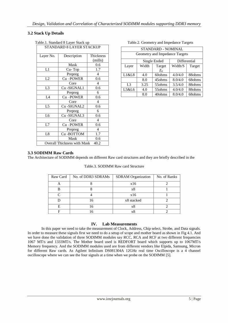
3.2 Stack Up Details
Table.1. Standard 8 Layer Stack up Table.2. Geometry and Impedance Targets
STANDARD 8 LAYER STACKUP
Layer No. Description Thickness
(mills)
Mask 0.6
L1 Cu- Top 1.7
Prepreg 4
L2 Cu –POWER 0.6
Core 4
L3 Cu -SIGNAL1 0.6
Prepreg 6
L4 Cu –POWER 0.6
Core 4
L5 Cu -SIGNAL2 0.6
Prepreg 6
L6 Cu -SIGNAL3 0.6
Core 4
L7 Cu –POWER 0.6
Prepreg 4
L8 Cu -BOTTOM 1.7
Mask 0.6
Overall Thickness with Mask 40.2
3.3 SODIMM Raw Cards The Architecture of SODIMM depends on different Raw card structures and they are briefly described in the
Table.3. SODIMM Raw card Structure
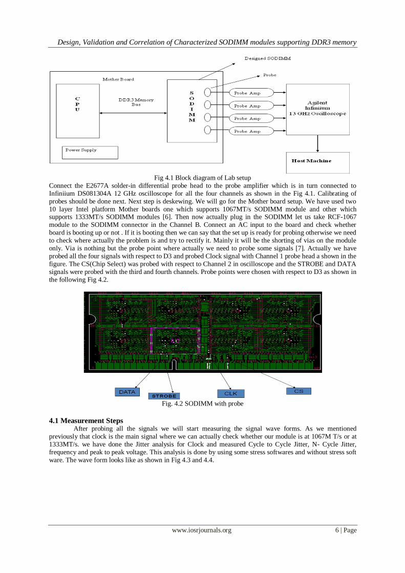
IV. Lab Measurements In this paper we need to take the measurement of Clock, Address, Chip select, Strobe, and Data signals.
In order to measure these signals first we need to do a setup of scope and mother board as shown in Fig 4.1. And
we have done the validation of three SODIMM modules say RCC, RCA and RCF at two different frequencies
1067 MT/s and 1333MT/s. The Mother board used is REDFORT board which supports up to 1067MT/s
Memory frequency. And the SODIMM modules used are from different vendors like Elpida, Samsung, Micron
for different Raw cards. As Agilent Infiniium DS081304A 12GHz real time Oscilloscope is a 4 channel
oscilloscope where we can see the four signals at a time when we probe on the SODIMM [5].
STANDARD - NOMINAL
Geometry and Impedance Targets
Single Ended Differential
Layer Width Target Z0
Width/S Target
L1&L8 4.0 60ohms 4.0/4.0 88ohms
8.0 45ohms 8.0/4.0 68ohms
L3 3.25 55ohms 3.5/4.0 88ohms
L5&L6 4.0 55ohms 4.0/4.0 88ohms
8.0 40ohms 8.0/4.0 68ohms
Raw Card No. of DDR3 SDRAMs SDRAM Organization No. of Ranks
A 8 x16 2
B 8 x8 1
C 4 x16 1
D 16 x8 stacked 2
E 16 x8 2
F 16 x8 2 DQ
Design, Validation and Correlation of Characterized SODIMM modules supporting DDR3 memory
www.iosrjournals.org 6 | Page
Fig 4.1 Block diagram of Lab setup
Connect the E2677A solder-in differential probe head to the probe amplifier which is in turn connected to
Infiniium DS081304A 12 GHz oscilloscope for all the four channels as shown in the Fig 4.1. Calibrating of
probes should be done next. Next step is deskewing. We will go for the Mother board setup. We have used two
10 layer Intel platform Mother boards one which supports 1067MT/s SODIMM module and other which supports 1333MT/s SODIMM modules [6]. Then now actually plug in the SODIMM let us take RCF-1067
module to the SODIMM connector in the Channel B. Connect an AC input to the board and check whether
board is booting up or not . If it is booting then we can say that the set up is ready for probing otherwise we need
to check where actually the problem is and try to rectify it. Mainly it will be the shorting of vias on the module
only. Via is nothing but the probe point where actually we need to probe some signals [7]. Actually we have
probed all the four signals with respect to D3 and probed Clock signal with Channel 1 probe head a shown in the
figure. The CS(Chip Select) was probed with respect to Channel 2 in oscilloscope and the STROBE and DATA
signals were probed with the third and fourth channels. Probe points were chosen with respect to D3 as shown in
the following Fig 4.2.
Fig. 4.2 SODIMM with probe
4.1 Measurement Steps After probing all the signals we will start measuring the signal wave forms. As we mentioned
previously that clock is the main signal where we can actually check whether our module is at 1067M T/s or at
1333MT/s. we have done the Jitter analysis for Clock and measured Cycle to Cycle Jitter, N- Cycle Jitter,
frequency and peak to peak voltage. This analysis is done by using some stress softwares and without stress soft
ware. The wave form looks like as shown in Fig 4.3 and 4.4.

Design, Validation and Correlation of Characterized SODIMM modules supporting DDR3 memory
www.iosrjournals.org 7 | Page
Fig. 4.3 Clock signal using RCF@ 1067MT/s
DDR3 signal definitions
tCK (avg) is calculated as the average clock period across any consecutive 200 cycle window, where each clock period is calculated from rising edge to rising edge.
tJIT(cc) is defined as the absolute difference in clock period between two consecutive clock cycles.
tJIT(cc) = Max of |{tCKi +1 - tCKi}|.
tJIT(N-Cycle) is defined as the difference in clock peiod when N number of Clock cycles are taken in
account.
Vp-p is the peak to peak voltage.
Next we will see how the clock wave forms look at RCF@1333 MT/s.
In the next step we have measured the Set up and Hold times for DATA and STROBE at 1067MT/s for RCC and RCF. But in this paper we are presenting the waveforms for RCF as shown in the Fig 4.5 and 4.6. This Data
pattern can be given by us using some software like MARS. For DDR3 we will be seeing worst case pattern for
AA, A0, 0A, F0, 0F and 88 in hex representation. When we give the Data pattern as AA(10101010), we can’t
see the pattern as it is an oscilloscope as it follows the little Endian criteria. So we will see the pattern as
(01010101).

Design, Validation and Correlation of Characterized SODIMM modules supporting DDR3 memory
www.iosrjournals.org 8 | Page
Fig. 4.4 Clock signal using RCF@ 1333 MT/s
Fig. 4.5 RCF_1067_DATA&STROBE _AA_RISE_SETUP
Fig.4.6 RCF_1067_DATA&STROBE_AA_FALL_HOLD

Design, Validation and Correlation of Characterized SODIMM modules supporting DDR3 memory
www.iosrjournals.org 9 | Page
V. Simulation Setup In order to correlate our Lab data with simulation data we need to do the simulations using HSPICE in
UNIX environment. In the deck, we are using the following full channel topology [8].The full channel topology
is shown in the Fig. 5.1.
Fig 5.1 Full Channel Topology
5.1 Analysis Setup Tools: HSPICE and JMP.
Base platform - Intel Huron River.
RCF- 2 Rank / 16 x8 SDRAM devices.
Speed- 1067MT/s.
All transmission line models are 10 line coupled models.
Models :
Clock – 26ohms/3.5V-nS used as driver.
RLC lumped model used as Receiver.
2D and 3D models used for different segments.
Clock is modeled as differential signal with two aggressors.
Data Strobe is differential and Data bits single ended in a 10 line coupled model [9].
Some of the Simulated Clock waveform (preliminary) for RCF is as shown below
Some of the simulated waveform of DATA and STROBE of AA and F0 for RCF is as shown below
Fig 5.2 RCF_1067_DATA&STROBE _AA
CPU Buffer
CPU Package Mother Board
S
O
D
I
M
M
D2

Design, Validation and Correlation of Characterized SODIMM modules supporting DDR3 memory
www.iosrjournals.org 10 | Page
Fig 5.3 RCF_1067_DATA&STROBE _F0
VI. Correlation Setup In the correlation part we will see that how the DDR3 signal groups like Clock, Data and Strobe Simulation
data matches with the Lab data. We have done the correlation part for the Clock of RCF at 1067MT/s and
1333MT/. And this correlation is done by taking the Lab csv file and simulation csv file into a new excel sheet
and plotted the following Fig. 6.1 and 6.2 using chart. And the time difference between the two points in the
data is 50pS.
RCF_1067_CLK
-1.00E+00
-8.00E-01
-6.00E-01
-4.00E-01
-2.00E-01
0.00E+00
2.00E-01
4.00E-01
6.00E-01
8.00E-01
1.00E+00
TIME(p
s)350
7501150
15501950
23502750
31503550
39504350
47505150
55505950
Lab Voltage
SIM Voltage
Fig 6.1 Correlated RCF_1067_CLK
RCF_1333_CLK
-1.00E+00
-8.00E-01
-6.00E-01
-4.00E-01
-2.00E-01
0.00E+00
2.00E-01
4.00E-01
6.00E-01
8.00E-01
1.00E+00
TIME 50
110170
230290
350410
470530
590650
710770
830890
LAB Voltage
SIM Voltage
Fig 6.2 Correlated RCF_1333_CLK
Next we have done the correlation part for the Strobe (DQS) and Data(DQ) of RCF at 1067MT/s for the pattern
AA which are shown below in Fig. 6.3 and 6.4.
STROBE
DATA

Design, Validation and Correlation of Characterized SODIMM modules supporting DDR3 memory
www.iosrjournals.org 11 | Page
RCF_AA_DQS
-8.00E-01
-6.00E-01
-4.00E-01
-2.00E-01
0.00E+00
2.00E-01
4.00E-01
6.00E-01
8.00E-01
0
450
900
1350
1800
2250
2700
3150
3600
4050
4500
4950
5400
5850
6300
6750
7200
LAB DQS
SIM DQS
Fig 6.3 Correlated RCF_1067_AA_STROBE
RCF_AA_DQ
0.00E+00
2.00E-01
4.00E-01
6.00E-01
8.00E-01
1.00E+00
1.20E+00
1.40E+00
TIM
E
350
750
1150
1550
1950
2350
2750
3150
3550
3950
4350
4750
5150
5550
5950
6350
6750
7150
LAB DQ
SIM DQ
Fig 6.4 Correlated RCF_1067_AA_DATA
VII. Conclusion Overall memory interface speeds are going up and in order to design and achieve next generation
memory performances, we need to understand SODIMM modules more closely.
To achieve the objective , we started with module design which involved
Selecting the relevant SODIMM module and speeds of operation.
Schematic design of the SODIMM module.
Carefully selecting the stack up details for the board design.
Completing necessary footprint creation and component placement in line with standard JEDEC
recommendations.
SODIMM board layout design with needed tools.
Manufacturing the module – by external vendor.
Validating the module with standard Intel mobile platform.
Understanding the measurements.
Simulating the same lab electrical case and correlating the results.
If we analyze the data in section 6, we can see that voltage level miscorrelation exists between lab data and simulation data. At the same time we have good correlation in rising and falling edge of signals which will
account for timing relationships between signals. This miscorrelation needs to be closely examined and rectified
to enable higher speed bins and performance levels of memory interface.
REFERENCES [1] Li, P. ; Martinez, J. ; Tang, J. ; Priore, S. ; Hubbard, K. ;Jie Xue ; Poh, E. ; Ong MeiLin ; Chok KengYin ; Hallmark, C. ;Mendez, D.
Development and evaluation of a high performance fine pitch SODIMM socket package, 1161 - 1166 Vol.1, IEEE,2004.
[2] PC3-6400/PC3-8500/PC3-10600/PC3-12800 DDR3 Un buffered SO-DIMM Reference Design Specification, Revision 0.71 draft.
[3] JEDEC STANDARD DDR3 SDRAM Specification (Revision of JESD79-3A, September 2007).
[4] PCB design tutorial and Orcad capture user guide.
[5] Infiniium DSO80000B Series Oscilloscopes and InfiniiMax Series Probes 2 GHz to 13 GHz Real-time Oscilloscope Measurement
Systems data sheet.
[6] Infiniium Series Oscilloscope Probes, Accessories, and Options Selection Guide Data Sheet.
[7] 1168A and 1169A InfiniiMax Differential and Single-ended Probes user guide.
[8] HSPICE® Simulation and Analysis User Guide Version Z-2007.03, March 2007.
[9] HSPICE Signal Integrity Guide U-2003.03-PA, March 2003.