porting the digital radio mondiale receiver on the...
TRANSCRIPT
Porting the Digital Radio MondialeReceiver on the Ericsson M7400
platform
By
Yang Liu
Final Project ThesisEindhoven University of TechnologyDepartment of Mathematics and Computer Science
Student:Yang Liu (0804638)[email protected]
Supervisor:Prof. Dr. ir. C.H.van BerkelEindhoven University of [email protected]
Tutor:Dr. ir. Peter de JagerSenior Software EngineerEricsson [email protected]

ii

iii
Abstract
Software Defined Radio (SDR) is a modern wireless communication tech-nology. In SDR, the software is implemented on general-purpose processorsto handle the communication tasks. Digital Radio Mondiale (DRM) is anew digital broadcasting standard using the SDR technology. This thesisconcerns the development of an embedded DRM receiver on the Ericssonplatform. The C++ code of the DRM receiver is from the Open Source PCsoftware, Dream DRM receiver. The Ericsson platform M7400 is selected asthe hardware to implement the embedded DRM receiver. The DRM code isported on the MSS (Modem Subsystem) of the M7400 platform to achievea DRM receiver program of the multi-core version. The MSS contains twoARM Cortex R4 processors and one EVP (Embedded Vector Processor) core.The EVP is a new generation DSP (Digital signal processor) of Ericsson.
The DRM code was firstly simplified and isolated in order to obtain a sim-ple, independent, compatible program running on PC and the program onlycontained the main DRM receiving process. Before porting the DRM pro-gram on the target platform, an intermediate step of porting the code on theCortex A8 Real-Time System Model(RTSM) was performed. The programwas then optimized based on the profile report of the program on CortexA8. After that it was ported on the Cortex R4 of the M7400 to achieve asingle-core version which cannot reach the real-time requirement. The multi-core version of the program was analyzed with the help of the analysis tool,Pareon from Vector Fabrics. Finally we ported Viterbi decoder function onEVP and developed the DMA communication between the ARM and EVPcore. Thus a embedded DRM receiver of the multi-core version was accom-plished on the M7400. It provided a speed up of 1.7X comparing with thesingle core version on the Cortex R4 and it could deliver a real-time service.
This project also shows that the ARM and EVP’s cooperating architectureon M7400 is suitable to process the SDR receiving task. And Pareon fromVector Fabrics is an appropriate tool in the analysis of the multi-core version.
Keywords: SDR DRM ARM EVP Multi-core Pareon DMA

iv

v
Abbreviations
DRM Digital Radio MondialeMSS Modem Sub SystemARM Advanced RISC MachineEVP Embedded Vector ProcessorRTSM Real-Time System ModelSDR Software Defined RadioOFDM Orthogonal Frequency-Division MultiplexingACC Advanced Audio CodingQoS Quality of ServiceCR Cognitive RadioSoC System on ChipNoC Network on ChipMLC Multi Level CodingSDC Service Description ChannelFAC Fast Access ChannelMSC Main Service ChannelRISC Reduced Instruction Set ComputingCISC Complex Instruction Set ComputingDMA Direct Memory AccessVA Viterbi AlgorithmHD Hamming DistanceBM Branch MetricPM Path MetricMCAPI Multi-core Application Programming InterfaceAXI Advanced eXtensible InterfaceAPB Advanced Peripheral Bus

vi

Contents
1 Introduction 1
1.1 Background of the Project . . . . . . . . . . . . . . . . . . . . . . . . . . . 1
1.2 Introduction of the Dream DRM Receiver . . . . . . . . . . . . . . . . . . 3
1.3 Introduction of the Ericsson M7400 platform . . . . . . . . . . . . . . . . 3
1.4 Problem Description . . . . . . . . . . . . . . . . . . . . . . . . . . . . . . 3
1.5 Outline of the thesis . . . . . . . . . . . . . . . . . . . . . . . . . . . . . . 4
2 Analysis of the DRM Receiver 7
2.1 DRM Receiver Outline . . . . . . . . . . . . . . . . . . . . . . . . . . . . . 7
2.2 Analysis and Isolation of the DRM receiver processing flow . . . . . . . . 10
2.3 DRM receiver’s benchmark . . . . . . . . . . . . . . . . . . . . . . . . . . 12
3 Background of the M7400 platform hardware 17
3.1 ARM . . . . . . . . . . . . . . . . . . . . . . . . . . . . . . . . . . . . . . . 17
3.2 EVP . . . . . . . . . . . . . . . . . . . . . . . . . . . . . . . . . . . . . . 19
3.3 On-Chip Communication . . . . . . . . . . . . . . . . . . . . . . . . . . . 21
4 Porting the DRM Receiver program on ARM 25
4.1 Porting the DRM receiver program on Cortex A8 . . . . . . . . . . . . . 25
4.2 Comparison of Cortex A8 and Cortex R4 . . . . . . . . . . . . . . . . . . 31
4.3 Porting the DRM receiver program on Cortex R4 . . . . . . . . . . . . . 33
4.3.1 Modifications of the DRM receiver program . . . . . . . . . . . . . 33
4.3.2 Profile results on Cortex R4 . . . . . . . . . . . . . . . . . . . . . 33
5 Analysis and Realization of the multi-core version 37
5.1 MLC and Viterbi Decoder’s working principles . . . . . . . . . . . . . . . 37
5.1.1 MLC encoder and decoder . . . . . . . . . . . . . . . . . . . . . . . 37
5.1.2 Viterbi Decoder . . . . . . . . . . . . . . . . . . . . . . . . . . . . . 40
5.2 Modification on the Viterbi decoder . . . . . . . . . . . . . . . . . . . . . 44
5.3 Pareon’s analysis in the multi-core version . . . . . . . . . . . . . . . . . . 46
5.4 Achieving the Viterbi decoder on EVP . . . . . . . . . . . . . . . . . . . . 56
6 Communication between the ARM and the EVP 63

viii
6.1 Programming on the DMA . . . . . . . . . . . . . . . . . . . . . . . . . . 636.2 Communication between the ARM and EVP with the DMA . . . . . . . . 66
7 Multi-core version Performance’s Estimation and Verification 717.1 Estimation of the Multi-core version Performance . . . . . . . . . . . . . 717.2 Profile results on the M7400 platform . . . . . . . . . . . . . . . . . . . . 77
8 Conclusion 818.1 Conclusion . . . . . . . . . . . . . . . . . . . . . . . . . . . . . . . . . . . 818.2 Future Work . . . . . . . . . . . . . . . . . . . . . . . . . . . . . . . . . . 82
Appendix A. ARM Linker configuration on Cortex R4 85
Appendix B. Multicore Communications API’s implementation 89

Chapter 1
Introduction
1.1 Background of the Project
As various wireless networks make up an increasing part of our daily lives, there is a bigdesire for the optimization in wireless communication systems. To begin with, moderncommunication technology standards define an extremely high transmission rate, whichis a challenge to the hardware to support a high data rate while minimizing the powerconsumption of the platform. Therefore, the hardware is required to perform well, bothin processing speed and power. Besides, another trend of the wireless communicationis to provide a seamless service over various wireless networks in a single device [1].However, the support of multiple protocols of various networks significantly increasesthe complexity of the communication task. This can be solved by using the software.The platform uses the general-purpose processor rather than the specific-purpose hard-ware. The software processing complex tasks of different services is implemented on thegeneral-purpose processor to support the communication. In short, a fully optimizedcommunication software and a well-performed platform are necessary for the implemen-tation of the wireless communication.
Software defined radio (SDR) is a modern software-based wireless communication tech-nology. It realizes modulation, encoding, filtering and other radio communication pro-cesses which are traditionally implemented by circuits, by means of the software on PC,cell phone or other computer systems [2]. The SDR supports multiple communicationprotocols including multi-band, multi-standard, multi-service and multi-channel. Thissoftware based implementation has some obvious advantages including ease of adaptationand flexibility over the traditional hardware based analogue radio [3]. Firstly, it is recon-figurable to provide a high adaptable service. The SDR can easily switch within modesaccording to the environment or user requirements [4]. In the transmitter end, it notonly transmits the signal but also configures settings according to the environment. Ifthe Cognitive radio (CR) is applied, which senses the environment and tracks changes,

2 CHAPTER 1. INTRODUCTION
the SDR automatically reacts on CR’s finds to characterize all possible transmissionchannels, propagation paths as well as modulation methods, and finds the best mode totransmit. Otherwise, the user can configure the transmitter by himself, motivated byhis own knowledge or detection of the environment. In the receiver end, it detects thetransmission mode and corrects possible errors. What’s more, some software tools areused to improve the quality of service (QoS) [5]. Secondly, in terms of the flexibility,the SDR can be easily redesigned for a new or changed protocol and the redesign costis obviously less than the traditional analogue radio.
In 2001, the European Telecommunications Standards Institute (ETSI) defined an Or-thogonal frequency-division multiplexing (OFDM) based SDR, known as Digital RadioMondiale (DRM). The working frequency of DRM is the same as the analogue radiosystem and it is divided into 2 modes, DRM30 and DRM+ [6]. DRM30 mode is de-signed to utilize AM broadcast bands below 30 MHz and DRM+ mode works above30 MHz, which is the FM band. The analogue radio system working on this frequencyrange has advantages of a large coverage area and relatively little interference caused bythe environment [7]. But it also has some disadvantages, low flexibility, service qualitylimitations as well as sensitive to interferences from the long-distance propagation. DRMinherits the advantages of the traditional radio and implements the digital technology,various transmission modes and different bandwidths to overcome the analogue system’sdrawbacks.
DRM’s main processes include OFDM modulation/demodulation, mapping/de-mapping,cell interleaving/de-interleaving and so on. DRM achieves these processing routines bysoftware. It has 4 transmission modes, namely Mode A, Mode B, Mode C and ModeD. These 4 modes are various robustness modes which suit different channel conditionsand the details can be seen in Table 1.1 from [7]. The ability to select from a range oftransmission modes is a key and revolutionary feature of DRM. This allows the broad-casters to balance or exchange bit-rate capacity, signal robustness, transmission powerand coverage [6]. The CR technology, as discussed above, has not been applied in DRMyet. Therefore, in response to any local changes in the environment, the DRM user candynamically changes robustness transmission mode without disturbing the audience.
Table 1.1: DRM’s 4 robustness transmission modes [7]Robustness Mode Typical Propagation Conditions
A Gaussian channels, with minor fading
B Time and frequency selective channels, with longer delay spread
C As robustness mode B, but with higher Doppler spread
D As robustness mode B, but with severe delay and Doppler spread

1.2. INTRODUCTION OF THE DREAM DRM RECEIVER 3
1.2 Introduction of the Dream DRM Receiver
In our project, the Dream DRM receiver is chosen as the implementation software target,which is an Open-Source software under the GNU General Public License (GPL). TheDRM software is a C++ program running on the personal computer (PC). It is designedto run under Mac OSX, Microsoft Windows and Linux. The start time of the projectwas June 2001 by the Institute of Communication Technology, Darmstadt University ofTechnology.
This software project implements a working software receiver with the basic featuresof DRM. The receiver runs in two modes, DRM and Analogue. In the DRM mode,it receives the DRM signals and provides the service which can be an audio service,possiblly with associated data or a data service. The audio service supports AdvancedAudio Coding (ACC) audio and AAC+ audio. The data service supports Electronicprogram guides (EPG), Multimedia Object Transfer (MOT) Slide Show, Broadcast WebSite and Journaline. In the analogue mode, it can only process the AM, FM analoguesignals.
1.3 Introduction of the Ericsson M7400 platform
The Ericsson M7400 is chosen as the target platform to port the Dream DRM receiver.The M7400 is one of the productions of the Thorium Modem Solution which aims toprovide modem platforms for smartphones, tablets and connected devices for the LTE(long-term evolutio), HSPA (High Speed Packet Access) market. It is chosen to port theDRM implantation on the Modem Sub System (MSS) of the platform. The MSS con-tains two ARM (Advanced RISC Machine) processors and one EVP (Embedded Vectorprocessor) processor. The ARM core is expected to process tasks with high complexitybut low data rate, for instance, protocol stack handling, user interfaces and applicationframeworks. High data rate tasks with generic parallel processing, especially vectoriz-able tasks are assigned to the EVP core. A good task scheduling on the platform, forsoftware which means a good multi-core version, will significantly increase the software’sperformance and greatly decrease the platform power consumption.
1.4 Problem Description
This project aims to map the DRM Dream receiver on the Ericsson M7400 platformincluding partitioning C/C++ code into ARM and EVP. In addition, the interface needsto be developed to achieve the communication between processors.
Previous researches of the multi-core DRM receiver’s implementation on embedded hard-ware platforms, provides us useful experiences in the project. The Hijdra project of NXP

4 CHAPTER 1. INTRODUCTION
contained a work of a DRM program mapping in the Hijdra architecture [8]. The DRMreceiver was executed on TriMedia and the Viterbi decoder took up 10% of the wholeexecution time. In order to improve the performance, the Viterbi decoder was sepa-rated from the receiver and mapped on a Viterbi accelerator. A 5% improvement inthe speed performance was achieved. Paper [9] also concerned the DRM program map-ping. It achieved a run-time mapping of a DRM program to a heterogeneous Systemon Chip (SoC). The platform consisted of multiple tiles of different types (e.g. ARM,FPGA, DSP, FPGA) interconnected by a Network-on-Chip (NoC). Partitioning a DRMreceiver into smaller independent blocks was done and tasks were mapped into differenthardware tiles.
The project is started with the DRM implementation’s source code downloaded from theDream DRM’s website and the System-C model of the target M7400 platform providedby Ericsson. Finally it is expected to achieve a embedded multi-core version of the DRMreceiver implementation on M7400. The main scope of this project is to port the DRMreceiver’s main processing code on the M7400 platform. Comparing to the related works,an additional goal of this project is to evaluate the EVP and ARM’s cooperating perfor-mance. The Vector Fabrics tool, Pareon is also involved in the analysis of the program’smulti-core version. Vector Fabrics [10] is a company which specializes in developingtools for the design and implementation of multicore, multi-threaded applications andembedded systems.
The project consists of these steps. An analysis and isolation work of the DRM receiverprogram is done at the beginning. Then an intermediate step of porting the DRM code onan ARM virtual processor with a fast simulation speed, is achieved. On the basis of theprofile report delivered in the intermediate step, some modifications must be done to thesource code. Afterwards, the modified DRM receiver is ported on the ARM core of thetarget M7400 platform. Based on the profile report on the target platform, a research ofthe multi-core version of the DRM program is done with the help of the software Pareon.It is excepted that a similar conclusion as in [8] can be delivered that the Viterbi decodershould be moved to another processor. The Ericsson company provides an EVP versionViterbi decoder. Based on the provided EVP code, a modified Viterbi decoding programsuiting the DRM receiver is created. After developing the communication between theEVP and ARM core with the DMA controller, the performance of the DRM receivermulti-core version is estimated and compared with the actual profile report running onthe target platform.
1.5 Outline of the thesis
Chapter 1 provides an introduction to the project and relative concepts including thesoftware and the target platform. In Chapter 2, an analysis of the target software, DRMreceiver is achieved. A detailed background of the hardware including the ARM CortexR4, EVP and on-chip communication is discussed in Chapter 3. The mapping work and

1.5. OUTLINE OF THE THESIS 5
profile report on the ARM Cortex A8 and Cortex R4 are presented in Chapter 4. Thisis followed by the description of Multi Level Coding (MLC), Viterbi decoder workingprinciples, analysis of the multi-core version by Pareon as well as implementation ofViterbi decoder on EVP in Chapter 5. The development of the communication can beseen in Chapter 6. The calculation process of the multi-core improving performanceestimation and the actual profile report are in Chapter 7. Finally the study ends withconclusions and future works in Chapter 8.

6 CHAPTER 1. INTRODUCTION

Chapter 2
Analysis of the DRM Receiver
In this chapter, the outline of the DRM receiver is shown and the functionality of eachmodule is described in 2.1. Subsequently, 2.2 presents the DRM isolation steps anddiscusses the data flow of the DRM main processing. Finally, the creation and usage ofthe benchmarks to check functional correctness and to analyze the real-time performanceare given in 2.3.
2.1 DRM Receiver Outline
As the DRM receiver’s main running target is the computer or the mobile device, low en-ergy consumption and easy implementation are required for these platforms. Therefore,there should be some constraint on the DRM signal. The bandwidth of a DRM passbandsignal is less than 20 kHz so that there won’t be a big pressure on the filtering process inthe DRM receiver. What is more, the number of carriers used in the OFDM-modulationis relatively small (max 460). In the OFDM-modulation process of the transmitter, theencoded data are modulated into OFDM symbols. Each OFDM symbol is constitutedby a set of carriers and these closely spaced orthogonal sub-carrier signals are used tocarry data. Thus the small amount of carriers result in a less heavy computational loadof de-modulation an OFDM symbol in the receiver [11].
The outline of the DRM receiver is given in Figure 2.1. There are 6 modules, namelyRF-reception, A/D-converter, OFDM demodulation, De-mapping, Channel decodingand Source decoding.
The antenna and RF-reception can use the same modules as the analogue radio.
The A/D-converter converts the analog signal from the RF-reception into the digitalsignal.
The OFDM demodulation involves a series of complex processing steps including Sam-

8 CHAPTER 2. ANALYSIS OF THE DRM RECEIVER
RF-recep
tion
A/D
con
verter
OFD
M
de
mo
du
lation
De-m
app
ing
Ch
ann
el d
ecod
ing
Sou
rce de
cod
ing
Audio
Service
Data
Figure 2.1: DRM receiver outline structure
ple Rate Correction, Synchronization, Channel Estimation and Demodulation. Thedetailed processing steps are as following [11], the first step is to correct the samplerate and then acquire a coarse frequency offset estimation without the detection of therobustness mode. Based on the received signal, the receiver detects the robustness modeand achieves the timing acquisition which means getting the position of OFDM signals.With the knowledge of the robustness mode and timing, the useful part of OFDM signalscan be extracted and demodulated. The first OFDM symbol of each frame contains ad-ditional pilots for frame synchronization. After obtaining frequency pilots, the receivercan call the frequency offset tracking to achieve the frame synchronization and get theframe from the signal. Now the beginning of the frame is obtained, so channel estimationand timing tracking can be called. With timing tracking, the obtained frame in framesynchronization is corrected. Thus the receiver obtains all the transmitter parameters,channel parameter and uses them to obtain demodulated signals. The dataflow chart ofthe OFDM demodulation can be seen in Figure 2.2.
The De-mapping processing stage follows the OFDM demodulation and it divides de-modulated signals into 3 channels, Main Service Channel (MSC), Fast Access Channel(FAC) and Service Description Channel (SDC), based on the cell mapping of the trans-mission frame. The detailed transmission frame structure can be seen in [7]. MSC is thechannel of the multiplex data stream which occupies the major part of the transmissionframe and it carries all the digital audio services, together with possible supporting andadditional data services. FAC is the channel of the multiplex data stream containing theinformation that is necessary to find services and begin to decode the multiplex. SDC isthe channel of the multiplex data stream which gives information to decode the servicesincluded in the multiplex and information to enable a receiver to find alternative sourcesof the same data [7].
A cell de-interleaving function is applied to MSC in the receiver. Because MSC is trans-ferred in a higher protection level than the other two channels by locating an additionalcell interleaving processing after the MSC channel encoding process in the transmit-ter. The cell interleaving routine is aimed at changing the possible burst error into therandom error which can be corrected by the receiver’s channel decoding routine. Theburst error means error occurs in contiguous sequence of symbols while for random er-

2.1. DRM RECEIVER OUTLINE 9
Sample rate correction
Start
Coarse Frequency Estimation
Detection of Robustness mode
Timing Acquisition
Know the frequency
Frequency offset correction
NO YES
Know the mode
NOYES
OFDM demodulation
Frame synchronization using pilots
Timing trackingChannel Estimation
Frame synchronizationSucessful?
Frame synchronization detection
NO
YES
Figure 2.2: OFDM demodulation’s dataflow chart

10 CHAPTER 2. ANALYSIS OF THE DRM RECEIVER
ror, error symbols are randomly located in the sequence. After interleaving, the adjacentcode blocks scatter. So adjacent error blocks are also separated and the burst error isconverted into the random error.
The Channel decoding processes MSC, FAC and SDC separately. The Channel decodingin DRM is multi level decoding including QAM de-mapping, Viterbi decoding and soon. In MSC, FAC and SDC, the decoding parameters are all different.
In the last stage Source decoding, the output bits of the Channel decoding are decodedinto audio, data or other services.
2.2 Analysis and Isolation of the DRM receiver processingflow
All the work and result of the DRM on PC is achieved on the Linux OS of a workstationusing an Intel i7 processor. Since the DRM receiver program has to be ported from thePC to an embedded system, it is not wise to port the whole original program. It is betterto delete some functions unnecessary on the target platform, to simplify the main DRMprocess for the purpose of achieving a minimal version of DRM receiver. Furthermore,an isolation work of the code related to the main DRM processing flow is finished onthe minimal DRM receiver in order to get a simple, independent and compatible DRMreceiver program. The structure of the expected DRM receiver program can be seen inFigure 2.3.
OFD
M
de
mo
du
lation
De-m
app
ing
Ch
ann
el d
ecod
ing
Decoded signal
Benchmark Source
Figure 2.3: DRM Receiver expected minimal structure
These steps have been done to achieve a minimal version of DRM receiver. Firstly,the Dream DRM receiver is built on our own PC’s Linux environment with supportedexternal libraries and building tools. An analysis of external libraries is done and itcomes to a conclusion that for the minimal version, the only external library neededis Libfftw, which is a library to provide the function of ”Fastest Fourier Transform”,and other libraries can be ignored. The details of the FFTW library can be referred to[12]. The relevant code of the Libfftw library is extracted and embedded into the mainfunction so that the main program can call the required functions of FFTW easily.

2.2. ANALYSIS AND ISOLATION OF THE DRM RECEIVER PROCESSINGFLOW 11
Secondly, the main program is simplified to isolate the DRM receiver function. Manyfunctions like GPS, DRMLogger, Graphical User Interface (GUI) and so on which runon PC, are not useful on the target platform. The original program has the code tosupport the function of the DRM transmitter, receiver and simulation of the wholeprocess from the sender via the channel to the receiver. In the receiver part, there arealso routines to support the analogue mode to receive and demodulate AM and FMsignals. These functionalities are not relevant to the main scope of the project, so theyare removed.
Finally, a further-simplification step on the main signal processing routine is imple-mented. The modules reading from the sound interface including audio file, soundcard, as well as decoding source and playing the decoded audio are removed from theflow.
A full image of the DRM receiver processing flow after these simplification steps ispresented in Figure 2.4.
In the part of OFDM demodulation, there are 6 stages, namely Input Resample, Fre-quency Synchronization Acquire, Time Synchronization, OFDM Demodulation, Syn-chronization using pilots and Channel estimation. OFDM cells are demodulated at theoutput of the OFDM demodulation. In the part of de-mapping, there is one processingstage, OFDM cell De-mapping. It separates the MSC, FAC and SDC off the carriers.The next part is Channel decoding, it decodes MSC, FAC and SDC separately. De-pending on the different importances of information channels, the decoding function ofvarious level complexity is applied to MSC, SDC and FAC separately. The decodingprocess of MSC is extremely complicated and costs much more time comparing with theroutine of FAC and SDC. The detailed working principle of decoding is discussed in sec-tion 5.1. What’s more, two more stages, De-multiplexer and De-interleave for cells areapplied for MSC channel decoding. The decoded SDC and FAC contain the informationon how to decode the MSC and how to find alternative sources of the same data, andgive attributes to the services within the multiplex [7]. Therefore, SDC and FAC areimported into the Utilization Stage to change the setting of the receiver.
Since the DRM receiver has to process the continuous real-time input and output datastream, the program uses the input driven processing sequence which means the processroutine is called when enough input data is delivered to the processing stage. There arebuffers between processing stages and they act as the input or output of the stage. Theprocessing stage checks its input buffer whether data is enough to call one routine. If so,it calls the processing function and exports the output data to the output buffer whichalso acts as the input of the next stage. Otherwise, the stage keeps on waiting. Twokinds of buffers are used in the program, namely single buffer and circular buffer. Thesingle buffer is used when the input block size of the buffer equals to the output blocksize. However sometimes the buffer needs a different input size and output size. In thiscase, the circular buffer is applied.

12 CHAPTER 2. ANALYSIS OF THE DRM RECEIVER
Figure 2.4: The minimal version of DRM receiver and its benchmark files
2.3 DRM receiver’s benchmark
The DRM dream project website provides some benchmarks to help developers andusers to check the functional correctness of the receiver. These benchmarks are antenna-received modulated digitized signals recording from the sound card interface of an inte-grated DRM receiver. The received signals are packed in the Wav file. Here the bench-marks containing audio services are chosen, because the audio service is the main serviceof the DRM and there is a strict processing time requirement on such service.
The received signals cannot be directly imported into DRM receiver processing stages.

2.3. DRM RECEIVER’S BENCHMARK 13
They must be processed in the stage of Read Data before demodulation. In the ReadData stage, it reads the signal recording file in the buffer in the type of 16-bit int andchecks the sample rate of the file from its header to see whether it is equal to the receiver’ssupporting rate 48000Hz. If unsupported, an additional resample has to be done. Thenaccording to the sound file’s audio channel setting, namely stereo and mono, an audiochannel process is used to produce a two channel signal stream. If the channel is mono,it extends the mono channel into a stereo channel by copying the values of the singlechannel to another channel. If the channel is stereo, it just copies the data. At last,the receiver handles the stereo channel data based on the receiver’s setting, the defaultsetting is mix channel. For the setting of mix channel, it converts stereo channeldata from 16-bit int type to 64-bit double type and then mix two channels by averagingtheir values. There are also other settings like left channel, right channel, I/Q inputand so on. Thus all the pre-processing routines are finished and the achieving data arestored in buffer DemodDataBuf. The DRM main processing function reads the data inbuffer DemodDataBuf and starts the main DRM processing.
At the output of the main DRM processing routine, information channels, MSC, FACand SDC, are obtained. It utilizes the information in FAC and SDC to change parametersand demodulation methods in the receiver and it decodes the MSC information into theaudio file and plays the audio. Using the GUI the information of the audio qualitycan be seen including signal-to-noise ratio (SNR) and weighted modulation error ratio(WMER) and delay. From paper [13], it can be concluded that audio dropouts detectableby non-professional listeners do not occur if the signal-to-noise ratio is greater than 17dB.
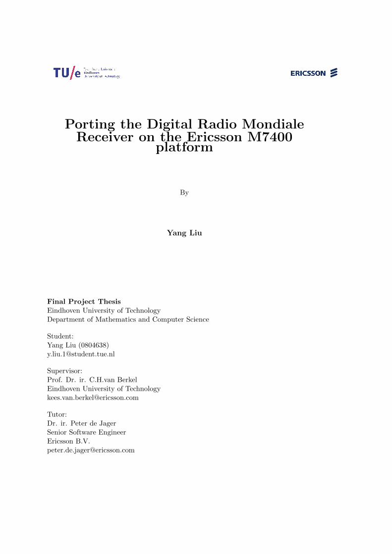
Three benchmark of received signals in different robustness modes, are chosen to test theoriginal receiver. The parameters of them can be seen in Table 2.1. These benchmarkfiles are used to test the receiver and all SNRs are larger than 17 dB. The detailed resultcan be observed in the evaluation dialog window. The detailed result including SNR,WMER and delay can be seen in Table 2.2. The delays which indicate the time periodbetween the launch of the software and the start of the audio service, are also acceptable.
Table 2.1: Benchmarks for the DRM receiverFile name Bandwidth sample rate Robustness Mode
received signals recording1 10kHz 48000Hz Mode B
received signals recording2 10kHz 48000Hz Mode A
received signals recording3 10kHz 48000Hz Mode C
Our minimal version of the DRM receiver only contains the main DRM process. Theinterface with different source inputs, decoding MSC and playing the audio are excluded.The chosen benchmarks cannot be directly processed to do the functional check of theprogram. The new benchmarks are created for the main DRM signal processing programbased on the original received signal benchmarks using the default setting in the Read
14 CHAPTER 2. ANALYSIS OF THE DRM RECEIVER
Table 2.2: Benchmark results for the DRM receiverFile name SNR WMER Delay
received signals recording1 31.8db 28.5db 0.82ms
received signals recording2 17.4db 17.7db 0.58ms
received signals recording3 21.2db 19.9db 0.82ms
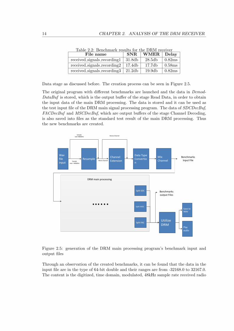
Data stage as discussed before. The creation process can be seen in Figure 2.5.
The original program with different benchmarks are launched and the data in Demod-DataBuf is stored, which is the output buffer of the stage Read Data, in order to obtainthe input data of the main DRM processing. The data is stored and it can be used asthe test input file of the DRM main signal processing program. The data of SDCDecBuf,FACDecBuf and MSCDecBuf, which are output buffers of the stage Channel Decoding,is also saved into files as the standard test result of the main DRM processing. Thusthe new benchmarks are created.
Wav file input
ResampleSample
rate≠48000Hz
Channel Extension
Sample rate=48000Hz
Mono Channel
Data Type Convertion
Stereo Channel
Mix Channel
Benchmarks Input File
Split SDC
Split FACUtilize DRM
Save to WAV
Play audio
Split MSC
…...
DRM main processing
Benchmarks output Files
Figure 2.5: generation of the DRM main processing program’s benchmark input andoutput files
Through an observation of the created benchmarks, it can be found that the data in theinput file are in the type of 64-bit double and their ranges are from -32168.0 to 32167.0.The content is the digitized, time domain, modulated, 48kHz sample rate received radio

2.3. DRM RECEIVER’S BENCHMARK 15
signal stream. In output files, there are 3 files for MSC, SDC and FAC separately anddata in files are binary in the type of 8-bit char. The DRM sends the information in theunit of frame and MSC, SDC and FAC bits are mixed in the frame. The program firstlydivides bits belonging to different information channels and then writes the divided bitsof one frame into output files for MSC, SDC and FAC. The details of benchmark filescan be seen in Table 2.3.
Table 2.3: Benchmarks for the DRM receiver’s main processing programFilename
type datatype
file size(byte)
framenum-ber
bit number perframe
original benchmark file
mytest1 input 64-bitdouble
28794880 - -
received signals recording11MSC output 8-bit
char4888800 175 6984
1FAC output 8-bitchar
52416 182 72
1SDC output 8-bitchar
158760 63 630
mytest2 input 64-bitdouble
13051656 - -
received signals recording22MSC output 8-bit
char2834400 75 9448
2FAC output 8-bitchar
22752 79 72
2SDC output 8-bitchar
81852 29 630 to 798
mytest3 input 64-bitdouble
22400368 - -
received signals recording33MSC output 8-bit
char506736 138 3672
3FAC output 8-bitchar
40608 141 72
3SDC output 8-bitchar
57792 49 282 to 630
In order to evaluate the modified DRM processing program’s demodulation and decod-ing quality, a tiny testing program is created to compare the MSC output with thebenchmark MSC output, frame by frame to measure the bit error and error rate in eachframe.
Besides functional correctness, it is also required to test the timing performance of theDRM program. The DRM receiver is a real time system and it is required to provide a

16 CHAPTER 2. ANALYSIS OF THE DRM RECEIVER
lasting audio service which means that the audio service will not be interrupted becauseof the unfinished processing of an audio frame. The DRM processing execution timeshould be less than its produced audio duration time so that a new audio stream isproduced before the end of the current playing audio stream.
One transmission frame contains one MSC frame and other SDC, FAC frames and theseSDC, FAC frames contain the information of how to obtain the MSC frame in the sametransmission frame. Thus, only the whole transmission frame is processed, the receivercan obtain the MSC frame. Each MSC frame is in the same size for each benchmark.After decoding, it generates the audio of the same time period. Therefore, based on theaudio stream duration and the MSC frame number, the audio stream duration per framecan be calculated, which can be seen in Table 2.4. It can concluded that audio streamduration per MSC frame is more than 400 ms. Considering the real time requirement, itmeans that the processing time of each MSC frame (equalling to the processing time ofthe whole transmission frame) should be less than 400 ms. However, for the first frame,there is no such requirement because the processing time of the first frame only resultsin a latency before the start of the service and will not influence the lasting audio.
Table 2.4: The audio stream duration per MSC framebenchmark input audio stream dura-
tionnumber of MSCframes
duration per MSCframe
mytest1 73420 ms 175 420 ms
mytest2 30814 ms 75 411 ms
mytest3 55629 ms 138 403 ms
In conclusion this chapter mainly describes the software. The background of the DRMsoftware is introduced and the detailed analysis, isolation work of the program and thecreation of the benchmarks are discussed. The introduction of the hardware is presentedin next chapter.

Chapter 3
Background of the M7400platform hardware
The background of the target M7400 platform hardware is introduced here. Since it ischosen to port the implementation on the MSS system, the structure MSS system of theM7400 is presented in Figure 3.1. The ARM processor (section 3.1), the DSP processorEVP (section 3.2) as well as the on-chip communication (section 3.3) are presentedrespectively in this chapter.
Figure 3.1: The MSS system of the M7400 platform
3.1 ARM
ARM architecture processors are a family of Reduced Instruction Set Computing (RISC)-based computer processors which are designed and licensed by the company ARM Hold-

18 CHAPTER 3. BACKGROUND OF THE M7400 PLATFORM HARDWARE
ings. Now ARM architecture processors are widely used in the electronic market. TheARM based product’s market share is more than 75% in mobile phone market, 25% inmobile computers and digital TVs, 50% in enterprise applications and less than 5% inMicrocontrollers/Smartcards in 2009 according to [14].
The original DRM software is aimed at personal computer which contains the proces-sor in X86 architecture rather than ARM. X86 is based on Complex Instruction SetComputing (CISC) which leads to the most essential difference comparing with ARM ofRISC.
The different instruction sets result in various characteristics of ARM and X64 proces-sors. On one hand, the ARM core has a simple hardware architecture, as a result theARM core has an obvious advantage in energy performance. The power saving advan-tage makes the ARM core suitable in embedded systems like the smart phone or TabletPC. On the other hand, the X86 processor especially Intel core’s complex hardware hasthe strength of execution speed so it is always used in computers and servers. A per-formance comparison between typical ARM and X86 processors is provided in paper[15]and [16]. In the first paper, the ARM Cortex A8 and Atom N330 are used to testbenchmarks . They are both aimed at embedded system, especially mobile processormarkets. With integer benchmarks, the Cortex A8 is slightly slower than the Atom N330in the benchmark performance per Mhz. However, the Cortex A8 performance is even100 times slower than the Atom N330 in double precision floating point benchmarks.The Cortex A8 deliveries a big advantage over the Atom N330 in power consumptionranging from 1 to 8 times power saving in most integer and double precision floatingpoint benchmarks. In paper [16], comparisons of Cortex A8 to Atom N450 and CortexA9 to Intel i7 are made. Considering the execution time, the A8 is about 4 times slowerthan the Atom and the A9 is approximately 7 times slower than the i7. But the A8 onlyconsumes one third power comparing with the Atom and A9 costs 20 times less powerthan i7.
In the target M7400 platform, the ARM core is Cortex R4. The Cortex R4 is aimedat deeply embedded system, which means the system is of big constraints in terms ofmemory, time and power consumption [17]. In a deeply embedded system the function-ality or the behaviour normally is not altered very often and the end user is not able tomodify, add or remove functionality to it.
The Cortex R4 was released in 2006 and is designed for semiconductor processes fromthe 90 nm node onward. The advanced semiconductor technology enables the Cortex R4to achieve a high performance with a limited clock frequency and power consumption.Besides the semiconductor technology, there are also many other features enhancing theCortex R4. It supports two instruction sets, ARM and Thumb-2. The ARM instructionset has comprehensive data-processing, control functions and a high performance. Onthe contrary, the Thumb-2 instruction set provides a higher code density, lower memorysize and cost but sacrificing the performance. Consequently, the ARM core can alter-nately use two instruction sets to execution different parts. Critical parts like handling

3.2. EVP 19
interrupts use ARM instruction sets to ensure the performance and insignificance partsare executed by the Thumb-2 instruction to reduce the cost [18]. The Cortex-R4 is alsohighly configurable. The configuration includes clock frequency, cache, Tightly-CoupledMemory Interface and so on. Therefore the hardware can be minimized according to therunning software to save the energy. The Cortex R4 also enables a quick response to aninterrupt ranging from 20 cycles to 30 cycles [19].
The Cortex R4 provides another version called Cortex R4F, which includes a FloatingPoint Unit (FPU) extension. The Cortex R4’s FPU is based on VFPv3-D16 (VectorFloating Point) architecture, which gives a full support of single-precision and double-precision arithmetic operations. It includes a register bank to support floating pointoperations. There are 2 views of the register bank, 16 double-precision 64-bit doubleword registers, D0-D15 and 32 single-precision 32-bit single word registers [20].
With FPU, the Cortex R4 processor’s application field expands, for instance, automotiveelectronics that uses sophisticated control algorithms, accurate image processing methodand other single precision floating point applications. What’s more, the existing softwarewritten in C/C++ or other high level programming languages , including floating-pointalgorithms, can be re-targeted to the ARM platform with less cost of the speed. Whenrequired, the FPU can perform double-precision (64-bit) floating-point calculations atthe expense of some calculation speed [19].
Without FPU, the Cortex R4 processor has to use the software to emulate floating pointoperations, which leads to a much higher time cost comparing with using FPU.
In summary, the Cortex-R4 processor delivers a high performance combined with costand power efficiencies across a broad range of deeply-embedded applications. CortexR4’s main application markets includes imaging and printing device, automotive systemcontrol, storage device driver and wireless communication device [19].
3.2 EVP
The EVP is a next generation Digital Signal Processor (DSP), which is designed forhigh computation applications such as 3G, 3.5G and Multimedia. It processes data inparallel as in the traditional DSP. Its processing speed can be up to 30 GPOS (30× 109
operations per second). Besides SIMD (Single Instruction Multi Data), it also supportsVLIW (Very Long Instruction Word). The maximum VLIW-parallelism available equals5 vector operations plus 4 scalar operations plus 3 address updates plus loop-control[21]. Some specific vector operations including Intra-Vector operation as well as Shuffleoperation, are also delivered by the EVP.
The EVP architecture combining SIMD and VLIW can be seen in Figure 3.2 frompaper [22]. The main word width is 16 bits and it also supports 8 and 32 bits. Thebit supporting design is based on the characteristic of the wireless protocol which is

20 CHAPTER 3. BACKGROUND OF THE M7400 PLATFORM HARDWARE
the main EVP application target. Since most wireless protocol’s algorithms operate onvariables with small values, 16 bits length is normally big enough.
Figure 3.2: The EVP architecture [22]
The main computation units in the EVP are divided into 3 groups, namely Scalar DataComputation Unit (SDCU), Vector Data Computation Unit (VDCU) and Address Com-putation Unit (ACU). VDCU contains Vector Load Store Unit (VLSU), Vector Arith-metic Logical Unit (VALU), Vector Mask Arithmetic Logical Unit (VMAU), VectorMultiply ACcumulate Unit (VMAC), Vector Shuffle Unit (VFU) and Intra Vector Unit(IVU). With the support of VDCU, EVP can process operations on all elements of thevector in parallel or operations within the elements of a single vector. In the SDCU,there are Scalar Load Store Unit (SLSU), Scalar Arithmetic Logical Unit (SALU), Pred-icate Arithmetic Logical Unit (PALU) and Scalar Multiply ACcumulate Unit (SMAC).SDCU provides the hardware to compute the single variable and it can work in parallelwith VDCU.
From the introduction of the EVP hardware, it can be seen that the EVP is good athigh-performance generic parallel processing. However it is not optimized for complextasks, for instance, real-time controlling, protocol handling and so on. It usually worksin the multi-processor system to co-operate with other processors. A typical multi-coresystem design and its task allocation can be seen in Figure 3.3. It can be concludedfrom the figure that high complexity tasks are executed in the ARM and DSP. Thelow complexity tasks with big bandwidth is assigned to the EVP and the hardwareaccelerator.
The EVP also performs well in the power consumption. Paper [22] shows that theEVP of 90nm running at 300 MHz generates a power of 1mW/MHz including a typicalmemory configuration. The EVP power performance can be compared with the Signalprocessing On Demand Architecture (SODA) which is also a DSP designed for the SDR

3.3. ON-CHIP COMMUNICATION 21
Figure 3.3: The task assignment of EVP-involved multi-core system
application. At 180nm, the power of SODA is 3W which is predicted to reduce to 250mW if 65 nm technology is applied [23]. Normally, a typical hand held wireless device hasa total power budget of 100 mW ∼ 300 mW [1]. Consequently, the energy performanceof EVP is in the same level as other SDR processors and it is suitable to be applied onthe handle device platform without a large power consumption.
3.3 On-Chip Communication
On-chip communication is an important element in the multi-core system since thecomponents of the system need to communicate with each other during the runningof the system. There are usually two requirements on the communication. The firstis that the communication must ensure a correctly and reliably data transfer. This isan essential demand for communication. Another requirement is the latency guaranteewhich implies that a data unit must travel through the communication architecture andreach its destination within a finite time determined by a latency bound [24]. The latencyis influenced by many factors including bandwidth, interconnect topology, comminationprotocol and so on.
The NoC (Network on Chip) of the target M7400 platform is bus. It is a simple archi-tecture and all components are connected to a shared bus. There is a Direct MemoryAccess (DMA) in the bus to control all kinds of data transfers including memory tomemory, peripheral to memory , memory to peripheral and peripheral to peripheral.Other master components write to DMA’s slave port to access to the DMA’s configura-tion registers and launch a transfer. After that, the master component is free and caninvolve in other tasks. While DMA’s master port will connect to the source and thedestination to control the transfer. The transfer initialized by DMA is the burst transferwhich sends multi-data in a burst with requesting only once for the access token, thusit can achieve a very high throughput comparing with other transfer modes.
There are some existing bus-based communication architecture standards which definedata transfer modes, protocols, bus architectures as well as component interfaces. Theapplication of the architecture standard will significantly speed up SoC integration and
22 CHAPTER 3. BACKGROUND OF THE M7400 PLATFORM HARDWARE
promote IP reuse over several designs [24]. Some popular architectures are listed here,ARM Microcontroller Bus Architecture (AMBA) 2.0, 3.0, IBM CoreConnect, STMi-croelectronics STBus and so on. The architecture applied in the target platform isAdvanced eXensible Interface (AXI) bus which is introduced in the AMBA 3.0 busarchitecture.
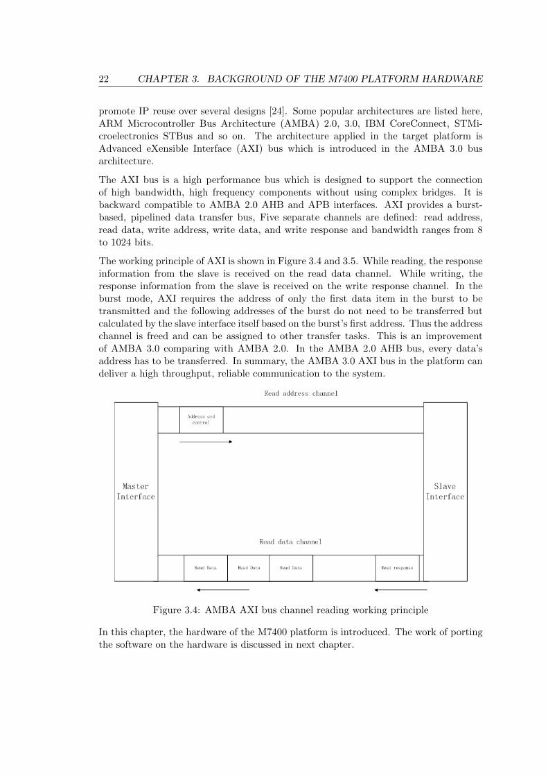
The AXI bus is a high performance bus which is designed to support the connectionof high bandwidth, high frequency components without using complex bridges. It isbackward compatible to AMBA 2.0 AHB and APB interfaces. AXI provides a burst-based, pipelined data transfer bus, Five separate channels are defined: read address,read data, write address, write data, and write response and bandwidth ranges from 8to 1024 bits.
The working principle of AXI is shown in Figure 3.4 and 3.5. While reading, the responseinformation from the slave is received on the read data channel. While writing, theresponse information from the slave is received on the write response channel. In theburst mode, AXI requires the address of only the first data item in the burst to betransmitted and the following addresses of the burst do not need to be transferred butcalculated by the slave interface itself based on the burst’s first address. Thus the addresschannel is freed and can be assigned to other transfer tasks. This is an improvementof AMBA 3.0 comparing with AMBA 2.0. In the AMBA 2.0 AHB bus, every data’saddress has to be transferred. In summary, the AMBA 3.0 AXI bus in the platform candeliver a high throughput, reliable communication to the system.
Figure 3.4: AMBA AXI bus channel reading working principle
In this chapter, the hardware of the M7400 platform is introduced. The work of portingthe software on the hardware is discussed in next chapter.

3.3. ON-CHIP COMMUNICATION 23
Figure 3.5: AMBA AXI bus channel writing working principle

24 CHAPTER 3. BACKGROUND OF THE M7400 PLATFORM HARDWARE

Chapter 4
Porting the DRM Receiverprogram on ARM
This chapter discusses the porting work on ARM. An intermediate step of porting theCortex A8 model is shown in 4.1. The comparison between the Cortex A8 processor andthe Cortex R4 processor is achieved in 4.2. Then based on the profile report on CortexA8 and the comparison conclusion, the DRM receiver needs to be optimized and portedon the Cortex R4 in 4.3.
4.1 Porting the DRM receiver program on Cortex A8
Before porting on the target platform, a intermediate step of porting on an easy trans-plant ARM core, is necessary for the reason that the software changes its running en-vironment from X86 to ARM. On the X86 processor, the compile tool is gcc while theprogram has to be compiled by armcc on ARM. Different compile tools and differentprocessor architectures may cause unexpected errors of the program, therefore a verifi-cation step to confirm the functional correct of the program on the ARM core is a need.As mentioned in 3.1, the processing ability of ARM architecture is obviously weakerthan that of the X86 architecture. The execution speed on the ARM may be signifi-cantly slower than on the PC, even cannot reach the real-time requirement. As a resulta measurement on the processing time is necessary.
The ARM Development Studio 5 (DS-5) supports debugging on Cortex-A8 Real-TimeSystem Model (RTSM). The RTSM helps users to debug the software on the ARMwithout the requirement for actual hardware. The model has already been installedthe Linux as the operation tool. The DS-5 tool will automatically link the applicationimage without user’s own boot file. The model’s running speed is also satisfactory. TheRTSM’s simulation time (the real world time) is a few minutes in running DRM programof processing 11 frames. However for the same workload, the System-C model of the

26 CHAPTER 4. PORTING THE DRM RECEIVER PROGRAM ON ARM
target platform takes more than two hours in actual time. Therefore, it is not wise todirectly debug on the the target platform’s System-C model. In RTSM, the absolutetiming accuracy is sacrificed to achieve the fast simulated execution speed. The modelcan be used for confirming software functionality, but the accuracy of cycle counts, low-level component interactions, or other hardware-specific behaviors are not reliable [25].Nevertheless, it is still a good reference to consider the coarse execution time. In short,the Cortex-A8 RTSM is a suitable platform to process a verification routine.
The DRM receiver is directly mapped on the Cortex A8 model without any modificationor optimized compile option. 3 benchmark inputs mytest1, mytest2 and mytest3 areimported into the program to do the functional check. All output results are 100%matched with the standard benchmark outputs.
The function gettimeofday can get the current time of Linux expressed in seconds andmicroseconds. Normally the time is transformed into millisecond to support a millisecondaccuracy measurement. The function can be allocated at the beginning and the endingof the target part to get the running time of the target. This is used to measure all thetime result in this section.
The Linux time function is used to measure the running time of ARM DRM receiver andthe result is compared with the receiver’s profile report on PC which is also achieved bythis function, gettimeofday. The comparison data can be seen in Table 4.1. It can beseen that the ARM version is as large as 300 times slower than the PC version. The ARMversion is extremely far away from the real-time service. For instance, in benchmark1,the processing time of each MSC frame is 3447 ms in average, which is about 10X largerthan 400 ms. As mentioned in 3.1, the ARM core’s ability in processing floating point issignificantly weaker than the Intel PC and the receiver program is written based on thefloating point algorithm where most variables are in the type of double precision floatingpoint. The floating point results in the long execution time on the ARM core.
Table 4.1: The execution time comparison of the DRM receiver on PC and Cortex R4modelbenchmark PC (X86) execution time (ms) ARM Cortex A8 execution time (ms)
mytest1 2432 589460
mytest2 1181 290907
mytest3 1325 349277
A study of the ARM core has been made to determine the optimization strategy. Aprogram computing the cumulative sum from 1 to 99999 is used as a benchmark to testthe simulation speed of the model dealing with different types of data. The result canbe seen in the 2nd column of Table 4.2. It shows that processing floating point takes100 times longer time than integer.
The default compile setting for the floating point is mfloat-abi=soft which means thecompiler generates output containing floating point software library calling for floating-

4.1. PORTING THE DRM RECEIVER PROGRAM ON CORTEX A8 27
Table 4.2: The cumulative sum testing program result on the Cortex A8 modeldata type execution time with
floating-point library(ms)
execution time withfloating-point hard-ware (ms)
int 1.6 1.6
float 93.9 5.6
double 117.8 5.7
point operations. From the result it can be concludes that the processing of the floatingpoint is extremely slow using the floating point function call.
There are 3 options for compiler to process floating point soft, softfp as well as hard.soft calls the library. softfp allows the generation of code using hardware floating-pointinstructions, but still uses the soft-float calling conventions. hard allows generation offloating-point instructions and uses FPU-specific calling conventions [26].
soft is slow and but is used when the ARM processor does not support floating pointhardware operations. Both softfp and hard generate hardware floating-point instructionswhich make floating-point instructions efficient. But when using hard, all the programsand libraries are required to be compiled using this option. softfp is chosen to enhancethe compatibility to benefit further extension development. Using the compile optionmfloat-abi=softfp, the execution speed of the testing program can be seen in the 3rdcolumn of Table 4.2. The execution speed for the floating point is significantly increasedwhen the floating point hardware operation is applied instead of calling library functions.What’s more, operations on the single precision floating point variable (float) and doubleprecision floating point variable (double) take almost the same time.
In order to obtain a detailed concept of the Cortex A8’s performance and FPU’s en-hancement, a comparison is made, between the Cortex A8 model using FPU and the PCin the ability in processing integer and floating point data. The benchmark, Dhrystonefrom [27] is chosen to test on the Intel i7 PC workstation and the Cortex A8 RTSM re-spectively to study their abilities of processing integer. The results are provided in thesecond column of Table 4.3. The VAX MIPS result is obtained by dividing the numberof Dhrystone routines per second by 1757. Similarly, the Whetstone from [28] is usedto test the floating point processing and the single precision and double precision resultcan be seen in 3rd and 4th column of the table. It uses Million Instructions executedPer Second (MIPS) to measure the performance. From the result, it can be seen thatthe Intel i7 has an extremely big advantage in processing data with integer, float anddouble types. It also can be concluded that the processing speed in float and doubletype is almost the same in the Cortex A8 FPU.
Based on the discussion of the floating point before, the DRM receiver program is re-complied using the option mfloat-abi=softfp. The generating floating point hardwareoperations are executed by the FPU of Cortex A8, VFPLite which is in the Vector

28 CHAPTER 4. PORTING THE DRM RECEIVER PROGRAM ON ARM
Table 4.3: The Dhrystone and Whetstone benchmark result on Cortex A8 RTSM andIntel i7 PC
Dhrystone ( VAXMIPS)
Single-precisionWhetstone (MIPS)
Double-precisionWhetstone (MIPS)
Intel i7 9517.6 2000.0 5000.0
Cortex A8 142.3 148.8 153.4
Floating Point v3 (VFPv3) architecture. The processing time of 3 benchmarks can beseen in the 2nd column of Table 4.4.
Table 4.4: The execution time comparison of the DRM receiver on Cortex R4 modelwith different compile options
benchmark using vfpv3 (ms) using vfpv3 and NEON (ms)
mytest1 80425 75469
mytest2 37712 35497
mytest3 47267 43752
There are still some spaces to further improve the performance of the program on theCortex A8 core because the Cortex A8 implements the NEON technology. It is a SingleInstruction Multiple Data (SIMD) extension which provides standardized accelerationfor media and signal processing applications. It supports data types including integer andsingle precision floating point. The code is re-compiled with option mfloat-abi=softfp and-mfpu=neon and -ffast-math. -ffast-math is used to speed up the program by sacrificingthe math precision. And NEON cooperates with VFP to enhance the performance. VFPcan be used for ”normal” (non-vector) floating-point calculations. Also, NEON does notsupport double-precision floating point so only VFP instructions can be used for that.The timing performance results can be seen in in the 3rd column of Table 4.4.
In the practical use of the benchmark, processing the whole benchmark input takes toomuch time especially on the model of the target platform. In the following work, onlypart of the benchmark is imported so that the process of generating the first 11 framesis analyzed and each frame contains a MSC frame.
A function correctness check of the receiver also has been done to the ARM version usingthe vfpv3 and NEON. The error rate testing program is implemented to evaluate thereceiver’s output. The error rate of 3 benchmarks can be seen in Figure 4.1. When usinghardware floating point operations to process floating point calculations, the calculationaccuracy is different from using software floating point library. In the receiving process,there is a synchronization process at the beginning of the demodulation routine and thesynchronization algorithm is written in floating point. The algorithm is sensitive to theaccuracy so it results in a different demodulated result at first few frames. However,with the process of the demodulation, the errors are corrected and the error rate in theMSC frame is decreased.

4.1. PORTING THE DRM RECEIVER PROGRAM ON CORTEX A8 29
Figure 4.1: MSC frame’s error rate of three benchmarks
Focusing on the timing performance, the time interval of generating each MSC frame ismeasured in Figure 4.2. The first MSC frame takes a much longer time comparing withthe following frames because the synchronization routine as well as some initializationfunctions have to be called in generating the first frame which cost a large amount oftime. After that generating each frame costs an approximately same time. Besides,another regular pattern is also discovered. Except the first frame, the processing time isrelatively larger in Frame 3, 6, 9 since the workload is bigger in generating these frames.A structure of the transmitted frame can be seen in Figure 4.3 [7]. A transmissionsuper frame contains 3 transmission frames. Processing the first transmission frame willgenerate the first MSC frame in the transmission super frame and the workload includsdemodulation and decoding of one MSC frame, one SDC frame and one FAC frame.However, in the 2nd and 3rd transmission frame, the computation load only includesone MSC frame and one FAC frame. Therefore, generating the first MSC frame of thetransmission super frame takes a longer time.
From the real-time view, it cannot provide a lasting service because the processing timeof some MSC frames, is longer than 400 ms though it is very close to the real-timerequirement.
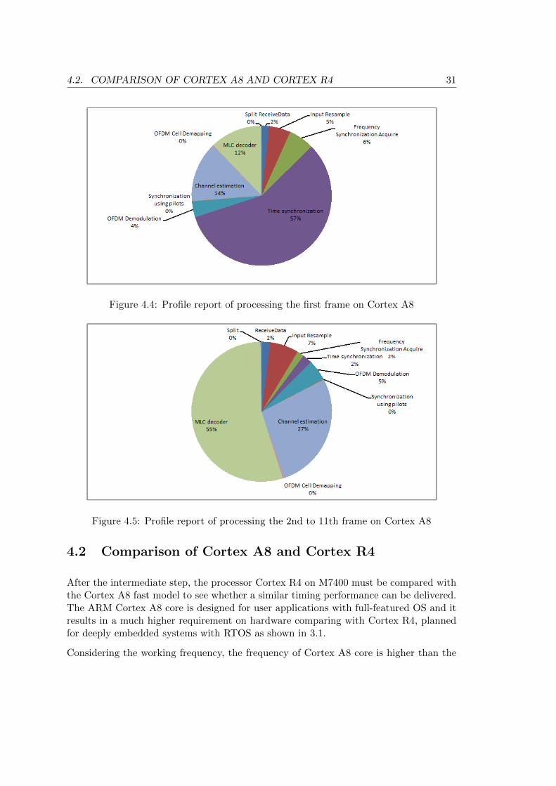
A profile report is achieved to observe the processing stages’ distribution in the wholeDRM receiver’s processing benchmark1 to generate 11 MSC frames. Since the functiondistribution in generating the first frame differs from the following process, they are dis-cussed separately. The profile report of generating the first frame is in Figure 4.4. From

30 CHAPTER 4. PORTING THE DRM RECEIVER PROGRAM ON ARM
Figure 4.2: MSC frame’s processing time on Cortex A8
Figure 4.3: The frame structure of the transmitted signals [7]
the pie chart, it can be seen that the synchronization routine, Time Synchronization,takes more than half of the running time. The profile report of generating the 2nd to11th frame is in Figure 4.5 where the distribution is rather different from Figure 4.4. Thechannel decoding function, MLC decoder takes 55% of the execution time. Among theMLC decoder, the processing function, Viterbi decoder occupies 91% of the decoder andthe Viterbi decoder holds 50% of the whole processing time. Although synchronizationtakes a lot of time in the first frame, it only results in the latency of the start of theservice which we are not interested in. Attention should be paid to the Viterbi decoderwhich is considered as a hot point needing to be optimized.
4.2. COMPARISON OF CORTEX A8 AND CORTEX R4 31
Figure 4.4: Profile report of processing the first frame on Cortex A8
Figure 4.5: Profile report of processing the 2nd to 11th frame on Cortex A8
4.2 Comparison of Cortex A8 and Cortex R4
After the intermediate step, the processor Cortex R4 on M7400 must be compared withthe Cortex A8 fast model to see whether a similar timing performance can be delivered.The ARM Cortex A8 core is designed for user applications with full-featured OS and itresults in a much higher requirement on hardware comparing with Cortex R4, plannedfor deeply embedded systems with RTOS as shown in 3.1.
Considering the working frequency, the frequency of Cortex A8 core is higher than the

32 CHAPTER 4. PORTING THE DRM RECEIVER PROGRAM ON ARM
Cortex R4 processor. Normally, it works at the frequency of 800 Mhz. On the otherhand, the frequency of the Cortex R4 processor on the M7400 platform is 416 Mhz.
For the floating point unit, the Cortex A8 contains a VFPLite co-processor which isan implementation of the ARM Vector Floating Point v3 (VFPv3) architecture with 32double-precision registers [29]. In the Cortex R4 processor on the M7400 real hardwareplatform, there is no FPU available. Therefore, the floating point library is applied whenprocessing floating point data types. It can be estimated that if the DRM receiver isported on the Cortex R4 without FPU, the execution time should be close to, or evenslower than the processing time of the Cortex A8 using the floating point library shownin Table 4.1. The execution speed on the Cortex R4 is unacceptable and it obviouslycannot achieve a real-time service. However, in the provided System-C platform model,the Cortex R4 processor is configurable. It can enable a FPU in the virtual hardware.After configuration, there can be a VFPv3-D16 in the same architecture as VFPLite butonly with 16 double-precision registers [20].
Since most part of the DRM code operates on floating point types, attention shouldbe paid in Cortex R4’s speed in processing floating point types. The single precisionand double precision Whetstone benchmarks are used as before in section 4.1. Andthe result is compared with that of the Cortex A8 shown in Table 4.5. The processingability of single and double floating point in Cortex R4 is weaker than Cortex A8. Andunlike Cortex A8, the Cortex R4’s ability in processing single-precision is obviouslystronger than double-precision. Therefore, a data type conversion from single-precisionto double-precision, is necessary for the program implemented on Cortex R4.
Table 4.5: The Whetstone benchmark result on Cortex A8 RTSM and Cortex R4 modelSingle-precisionWhetstone (MIPS)
Double-precisionWhetstone (MIPS)
Cortex R4 147.9 123.8
Cortex A8 153.4 148.8
What’s more, the Cortex A8 architecture contains a NEON co-processor which furtherenhances the processing ability. This SIMD technology is not applied in Cortex R4.
A signal processing kernel speed testing is presented in [30] using Certified BDTI DSPKernel Benchmarks. It shows that the Cortex A8 working at 450 Mhz delivers an almostthree times the performance of the Cortex R4 of 300 Mhz.
As far as the comparison achievement is concerned, the receiver mapping on CortexR4 cannot provide a similar timing performance as on Cortex A8. Therefore, somemodifications must be done to the program to speed up. The optimization of the programis presented in next section 4.3.1.

4.3. PORTING THE DRM RECEIVER PROGRAM ON CORTEX R4 33
4.3 Porting the DRM receiver program on Cortex R4
4.3.1 Modifications of the DRM receiver program
On the basis of the conclusion in 4.2, the code must be modified to speed up the re-ceiver.
As mentioned in 4.1, the widely used double precision floating type is the essential reasonof slowing down the ARM execution. There are two options for data type conversion.First is to transfer double precision floating point to integer, which is not realistic becauseit would have a lot of work including debugging overflow and changing to an integer fftwlibrary. Another option is to change double precision floating point into single precisionfloating point. This would also enhance the performance based on the processor’s resultshown in Table 4.5. Furthermore, the problems caused by converting into integer do notappear. Thus the latter option is chosen in this study.
The time expensive part, Viterbi decoder function also needs to be optimized. TheViterbi decoder is re-written in integer and a scaling processing is done to the soft-decision inputs. The working principle and modification details of the Viterbi decoderis discussed in 5.2.
4.3.2 Profile results on Cortex R4
For porting on the Cortex A8 model, the DS-5 software will automatically link the ARMimage to the processor and begin the execution. However, the provided platform modelis written in System-C and is launched in the software, Synopsys Virtual PrototypeAnalyzer G-2012.06-SP2. The boot file has to be written using the ARM Linker toload the application image to the processor’s memory. The details of the ARM linkerconfiguration is presented in Appendix A.
Since the Cortex A8 model contains the Linux operation system, it is easy to control theinput and output of the data stream to read/write from/to files with the help of the op-eration system. However, the Cortex R4 System-C model is built without any operationsystem. Semihosting [31] is implemented here to communicate input/output requestsfrom application code to the host running a debugger which is the Synopsys softwarehere. The requests includes keyboard input, screen output, and disk I/O. When a re-quest occurs, the application invokes the appropriate Software Interrupt (SWI) and thenthe debug agent handles the SWI exception and communicate with the host. After that,the host responses to the debug agent’s communication information to export/importthe data stream.
The modified DRM receiver program is successfully ported on the Cortex R4 core ofthe platform model based on the configuration as discussed before. As mentioned in4.2, the core model setting has to be changed to enable VFU and the compile option

34 CHAPTER 4. PORTING THE DRM RECEIVER PROGRAM ON ARM
–fpu=vfpv3 d16 is used to configure the compiler to generate floating point hardwareoperations for vfpv3 d16.
A functional check of the modified code is achieved as it is done in Cortex A8 model insection 4.1. And the results can be seen in Figure 4.6. Comparing with Figure 4.1, theerror rate is slightly increased, but still acceptable.
Figure 4.6: The modified program running on Cortex R4’s MSC frame error rate of threebenchmarks
The software, Virtual Prototype Analyzer automatically provides a function traced pro-file report. It is used to measure the time in all timing results of the M7400 plat-form.
A similar timing performance measurement is finished as in Cortex A8 model using thebenchmark 1. The time interval of generating each MSC frame is measured in Figure4.7. Comparing with Figure 4.2, the processing time is larger than that of the CortexA8. Though some modifications are already applied to the source code to speed up, itstill cannot achieve a real time service since the processing time of each frame is above400 ms.
Profile reports based on benchmark 1 are achieved as it is done on Cortex A8 for theresearch on the function distribution on generating 1st MSC frame and generating 2ndframe to 11th frame respectively and the results are presented in Figure 4.8 and Figure4.9. The hot spot Viterbi decoder in Cortex A8 version is still the most time expensivepart which takes 78% of the MLC decoding time and 45% of the whole running time in theperiod of processing 2nd to 11th frame. Therefore, in order to increase the performance,

4.3. PORTING THE DRM RECEIVER PROGRAM ON CORTEX R4 35
Figure 4.7: MSC frame’s processing time on Cortex R4
attention should be paid to Viterbi decoder to further decrease the execution time.
Figure 4.8: Profile report of processing the first frame on Cortex R4
In this chapter, an intermediate step of porting the DRM program on the Cortex A8is done at first. Then the program is modified in order to speed up the execution.However, the details of the optimization on the Viterbi decoder is not shown in thischapter. Finally it shows the profile report of the optimized DRM program on theCortex R4 model. The optimized single core version still cannot reach the real-timerequirement in the Cortex R4. Therefore, a multi-core version should be achieved inthe following chapters. Furthermore, in the next chapter, the detailed modification tothe Viterbi decoder of the single-core version is also discussed in section 5.2 after the

36 CHAPTER 4. PORTING THE DRM RECEIVER PROGRAM ON ARM
Figure 4.9: Profile report of processing the 2nd to 11th frame on Cortex R4
introduction the working principle of Viterbi decoder in section 5.1.

Chapter 5
Analysis and Realization of themulti-core version
According to the conclusion in section 4.3.2, the Viterbi decoder slows down the wholeprocessing speed. Therefore, in the multi-core version, this part is a candidate to porton EVP. However it still needs to be considered if its related functions also have to beported on another core. Thus a discussion of MLC and its belonging Viterbi decoder’sworking principles must be done in section 5.1. Then upon the Viterbi decoding’s work-ing principle, section 5.2 shows the detailed modification of the Viterbi decoder of theARM single core version as discussed in section 4.3.1. The tool Pareon is used in analysisof the multi-core version of the program and it will be discussed in section 5.3. Based onthe analysis result, section 5.4 presents the realization of the ported code on EVP.
5.1 MLC and Viterbi Decoder’s working principles
5.1.1 MLC encoder and decoder
In the transmitter end, the MLC encoding is applied in the channel encoding process.In MLC, the source bit stream is partitioned into different streams. Each stream goesthrough the encoding processes respectively and then converges together to do QAM(quadrature amplitude modulation).
The processing flow is shown in figure 5.1. The source information is encoded into bitstream before importing into the MLC routine. In the MLC encoding processing stage,the Energy Dispersal is the first processing function. The purpose of this function is toavoid the transmission of signal patterns which might result in an unwanted regularityin the transmitted signal [7]. A scrambler is used here to convert the bit stream intoa seemingly random bit stream of the same length by using a pseudo-random binarysequence (PRBS), thus avoiding long sequences of bits of the same value.

38CHAPTER 5. ANALYSIS AND REALIZATION OF THE MULTI-CORE VERSION
Figure 5.1: The processing flow of 3 level MLC encoder in the DRM transmitter
Then according to the robustness mode setting of the transmission, the bit stream isdivided into n levels in the Partitioning function. n ranges from 1 to 3.
Each partitioned bit stream is encoded separately. The convolutional coding with aoriginal code rate 1/4 and constraint length 7 is applied. The codeword is defined as theequation 5.1. The structure of convolutional encoder can be seen in figure 5.2 from [7].Every 1 bit inputs into the encoder, it will generate 4 bits output. Therefore, the coderate is 1/4. There are 6 shift registers in the decoder, as a result 7 bits in the encoderare involved in calculating the output bits. So the constraint length of the encoder is7.
b0,i = ai⊕ai−2
⊕ai−3
⊕ai−5
⊕ai−6
b1,i = ai⊕ai−1
⊕ai−2
⊕ai−3
⊕ai−6
b2,i = ai⊕ai−1
⊕ai−4
⊕ai−6
b3,i = ai⊕ai−2
⊕ai−3
⊕ai−5
⊕ai−6
(5.1)
However, if the original encoder’s code rate is directly put into use, a large amount ofoutput bits are generated and it gives a significantly large burden on the transmitterand receiver. Therefore, a puncturing processing to output bits is necessary in orderto decrease the code rate. Various puncturing patterns are stored and applied to theconvolutional output bits to remove some of the parity bits without influencing theerror-correction ability.
Bit-wise interleaving shall be applied for some of the streams. The punctured bits areinterleaved according to the corresponding interleaving table.
Finally, the divided bit streams are converged in the QAM function. In QAM, the con-stellation points are usually arranged in a square grid with equal vertical and horizontal

5.1. MLC AND VITERBI DECODER’S WORKING PRINCIPLES 39
Figure 5.2: The structure of convolutional encoder in the DRM transmitter [7]
spacing and the number of points in the grid is usually in a power of 2. In this module,the number of point is decided by the bit stream level n. The point number equals 4n,therefore 4-QAM, 16-QAM and 64-QAM are implemented here. In each mapping, 2 bitsare extracted from each divided stream to act as the vertical and horizontal coordinates.Since the stream number n matches the QAM size, the extraction bits of n streams aresuitable to process a mapping at the constellation which can be seen in Figure 5.3.
Figure 5.3: The multi level QAM mapping working principle
Based on the channel encoding process, a corresponding channel decoder is built inthe receiver end. The MLC decoding is also named multistage decoding (MSD). Thedecoding is an iterative process which means the lower level decoding result will be ofhelp to decoding the higher level bits as seen in Figure 5.4.
The data flow structure of MLC decoding can be seen in Figure 5.5. One decoding routine

40CHAPTER 5. ANALYSIS AND REALIZATION OF THE MULTI-CORE VERSION
includes QAM de-mapping, Bit de-interleaving, De-puncturing and Viterbi Decoder.After decoding ,the decoded bits are imported into the encoding routine which consistsof the same processing functions as in the encoder of the transmitter. The encodedbits are iteratively imported back to the QAM de-mapping function and work as thedetermined bits to help estimate the bits of the next level.
Figure 5.4: The iterative decoding process of MLC decoder
Figure 5.5: The processing flow of MLC decoder in the DRM receiver
There is an iterative number parameter that effects the decoding times of each outputbit. In the DRM receiver, the default setting of this parameter in the MLC decoder is 2which is applicable to 2 levels and 3 levels MLC decoder. For instance, in 2 level MLCdecoder, 2 data streams X and Y are decoded. The X stream is firstly decoded and thenthe X result helps in decoding the Y stream. This is the first iteration. In the seconditeration, the Y stream result from the last iteration, helps the re-decoding work of X,and the final result of X stream is obtained. The final result of X stream helps decodethe Y stream. However, as to the 1 level MLC decoding, since it only contains one bitstream, even if it iteratively inputs into the decoder, it cannot be helpful in the 4-QAMde-mapping. The output bit of the 1 level MLC decoder is decoded only once.
5.1.2 Viterbi Decoder
Among all the processing functions in the MLC decoder, the most time-expensive partis Viterbi Decoder. A detailed working principle of the Viterbi decoder is discussedbelow.
There are two parts in the decoder, namely trellis construction and trace back. In the

5.1. MLC AND VITERBI DECODER’S WORKING PRINCIPLES 41
decoder, Viterbi Algorithm (VA) is used to find a maximum likelihood (ML) estima-tion of a transmitted code sequence c from the received sequence r by maximizing theconditional probability P (r|c).
In the trellis construction, the Branch Metric (BM) is used to present the conditionalprobability of one encoding branch based on the received encoded bit sequence. Twomethods can be used to present the received encoded bit, namely Hard-Decision andSoft-Decision. In the Hard-Decision, each received encoded bit is presented by 1-bitquantized decoder input. Then the BM of a branch is obtained by calculating theHamming Distance between the decoder inputs and the encoding bits of the branch.Hamming Distance stands for the number of differing bits between two bit sequence.The smaller BM indicates that the the decoder inputs is more closed to the encodingbits of the branch, thus the possibility of this branch is higher. While for Soft-Decision,it is basically the same as the Hard-Decision, but it improves the decoding quality byusing multi-bit quantized inputs to present each received encoded bit.
The Soft-Decision is applied in the Viterbi decoder of DRM. The multi-bit quantizedinput is calculated by multiplying the distance of the QAM constellation which is gottenfrom QAM de-mapping function and the magnitude of the channel achieved by thechannel estimation stage. Since puncturing is used, the puncturing pattern should alsobe considered. A table containing the puncturing pattern for each decoding bit is createdbefore the MLC decoding routine. There are 6 types of puncturing patterns, namely0000, 1111, 0111, 0011, 0001, 0101. 0 stands for un-punctured bit and 1 is for puncturedbit. For example, 0000 pattern means all 4 bits are not punctured, thus 4 inputs areinvolved in calculating BM. From this analogy, if the puncturing pattern is 0001, 3 inputsare used to decide BM. Thus based on the multi-bit quantized input and the puncturingpattern, the difference between the received bits and every possible branch’s encoderbits can be measured out.
Path Metric (PM) is the sum of the corresponding BMs. If two branches merge at astate, the smallest one is chosen to survive. A whole process of trellis construction canbe seen in Figure 5.6. It is a decoder with the code rate 1/3, constraint length 3 andthe Hard-Decision is applied. The states of 00, 01, 10, 11 present the bits store in theencoder register. Each state has two branches. The solid line branch is for the encoderinput bit 0 and the dotted line branch shows the encoder input bit 1. The bits on thebranch presents the corresponding encoder output. The received bits’ (decoder inputbits) HB with every branch are computed to obtain the BMs shown in red italic. PMis located in every state shown in black bold. If two branches merge at a state, thesmallest one is chosen to survive as it is in state 00 in step 3. If choosing the branchfrom state 00, the resulting PM is 5. However, if choosing the branch from state 10, PMis 1. Therefore, the latter path is selected and PM is calculated as 1. The path decisionis stored in the decision bit.
Therefore, in every trellis construction step, all the BMs are calculated and added withthe corresponding PM. The confluent branches are compared to remain the smaller one

42CHAPTER 5. ANALYSIS AND REALIZATION OF THE MULTI-CORE VERSION
Figure 5.6: The processing of the trellis construction
and the decision bit is stored. This process results in an high computational load. Inthe DRM Viterbi decoder, the constraint length is 7. Based on this, a computation loadis listed in Table 5.1. The Viterbi decoder’s trellis step number n is equal to the numberof the decoding output bits. In the implementation, normally the trellis step can be upto 4000, which leads to a significantly large number of calculation.
Table 5.1: The computation load of the n-step Viterbi decoder of DRMAddition operation Comparison operation Store operation
128× n 64× n 64× n
Since the PM is a result of thousands times of repeated additions, the value may beextremely large which needs a large register to store. However, if the hardware is limited,some methods must be done to prevent the overflow. Four normalization methods arelisted in [32], Reset Metric Normalization, Variable Shift Metric Normalization, FixedShift Metric Normalization, and Modulo Metric Normalization. Normalization is noteasy to implement and it will slow down the processing speed due to its periodic checkingoverflow. But it has an obvious advantage that it will not decrease the decoding accuracybecause it is the difference values between PMs that decides the decoding output ratherthan the absolute values. An alternative option is scaling. If the maximum number ofsteps is already known, based on the max steps n and register width, a scaling operationcan be done to the BMs to ensure that even if the maximum BM value is repeatedlyadded n times, the accumulate value should not overflow in the register. The advantageof scaling is that the implementation is easy and it won’t influence the decoding speed

5.1. MLC AND VITERBI DECODER’S WORKING PRINCIPLES 43
because the scaling is processed before the Viterbi decoding. However, the scaling willinfluence the accuracy of the decoding, since the scaling of BM will decrease or increasethe difference values between PMs.
In the trace back part, the most likely sequence is reconstructed by going back in stepsand the processing can be seen in Figure 5.7. There are two methods in trace back. Thefirst approach is sliding window. The timing relation between the Trellis constructionand the trace back can be seen in Figure 5.8. One time trace back of a constant lengthDback occurs periodically and the period is a certain number Dforward trellis constructionsteps. In trace back, the smallest PM is chosen as the starting point and construct apath backward in the length of Dback based on the decision bits. At every turn oftrace back, Dupdate decoding bits are exported (Dupdate = Dforward). Furthermore, inpractical implementation, the trellis construction can execute in parallel with the traceback.
Figure 5.7: The processing of the trace back
A second approach uses frames. With frames, the dependency chain is the length of theframe [33]. In the encoding, the input bits of a frame is ended with a sequence of 0.Trace back only happens once when the trellis construction of the whole frame ends. Atrace back from the ending to the beginning of trellis steps is done to decode the wholebits in one time. And the starting point is chosen in the state with all 0, since the endingof the frame is a sequence of 0.
Comparing these two approaches, the sliding window method uses less memory. Thedecision bits of the already decoded bits do not need to be stored in the memory. An-other advantage is that it can process faster because of the parallel execution of trellis

44CHAPTER 5. ANALYSIS AND REALIZATION OF THE MULTI-CORE VERSION
Figure 5.8: The timing relation between Trellis construction and trace back of slidingwindow
construction and trace back. However, the speed advantage is not obvious because thetime cost of the trace back is greatly smaller then that of the trellis construction. Whilethe frame based trace back method delivers a higher error correction decoding becausethe multi-time trace back will inevitably cause error. In the sliding window, the traceback path is built based on the current constructed trellis but if the unestablished trellisare taken into consideration, a rather different path may be built.
5.2 Modification on the Viterbi decoder
Section 4.3.1 presents that the variables of the whole program are converted from 64-bitdouble to 32-bit float at first. Then the Viterbi decoder function is optimized in theARM Cortex R4 single-core version. However, the detailed optimization steps in Viterbidecoder are not shown. In this section, we work on the 32-bit float version program and

5.2. MODIFICATION ON THE VITERBI DECODER 45
the data type conversion and scaling process are discussed combining with the workingprinciple shown in section 5.1.
To decrease the execution time of the Viterbi decoder on Cortex R4, the first step is torewrite the function from 32-bit float to 32-bit int. As mentioned in 5.1, the relativevalues of PMs decide the decoding results, therefore a type conversion on BMs fromsingle precision floating point type to integer will not significantly decrease the decodingaccuracy. The conversion is achieved by using Vint = floor(Vfloat + 0.5) to round thedecimals to the nearest integral number. A result can be seen in Figure 5.9 testing onthe PC version of the DRM receiver to observe the type conversion’s influence on thereceiver’s MSC outputs.
Figure 5.9: MSC frame error rate tested by three benchmarks of the single precisionfloating type version program with integer Viterbi Decoder
Based on the integer Viterbi decoder version, a scaling to the soft-decisions is furtherachieved to prepare porting the Viterbi decoder code on EVP. When it is implementedon EVP, an overflow problem may occur. The range of BM should be limited to preventits accumulation result, namely PM over the range. In the integer conversion process,the BMs are converted from the 32-bit float to 32-bit int. However, the soft-decisioninputs are still in 32-bit float to guarantee the precision of the decoder. It is chosen toscale the soft-decision input before de-puncturing processing. Since BM is calculated bysoft-decision inputs, the value of BM can be controlled when the value of the soft-decisionis restricted.
Before de-puncturing, the soft-decision inputs for a single Viterbi decoding routine are

46CHAPTER 5. ANALYSIS AND REALIZATION OF THE MULTI-CORE VERSION
searched to find the max value Imax. If it is bigger than the Smax, the scaling factoris calculated by Sfactor = Imax/Smax and then the scaling factor is used to scale theinput value by Iscale = I/Sfactor. Otherwise, inputs are unprocessed. Since scaling willdecrease the accuracy as shown in 5.1, it is necessary to find a proper scaling degree. Asimilar testing on the MSC error rate in different Smax is finished and the result can beseen in Table 5.2. The used benchmark is mytest2 because it is in the lowest protection,Robustness Mode A. If this benchmark can be decoded with low error rate, others canalso be processed successfully. It can be seen when Smax is decreased to 2, the error rateis greatly increased and the error extents to the latter frames. The calculation result forEVP shown in 5.4 presents that when Smax is 3, the PM will not overflow in a 16-bitregister. Therefore, Smax is chosen as 3.
Table 5.2: The single precision floating type version, integer Viterbi decoding DRMreceiver’s MSC error rate in different Smax
MSC Frame ID 1 2 3 4 5 6 7 8 9 10 11
not applied (error rate %) 9 11 6 0 0 0 0 0 0 0 0
Smax 200 (error rate %) 9 11 6 0 0 0 0 0 0 0 0
Smax 100 (error rate %) 9 12 6 0 0 0 0 0 0 0 0
Smax 50 (error rate %) 8 11 4 0 0 0 0 0 0 0 0
Smax 10 (error rate %) 15 20 12 0 0 0 0 0 0 0 0
Smax 5 (error rate %) 18 31 21 0 0 0 0 0 0 0 0
Smax 3 (error rate %) 18 31 33 0 0 0 0 0 0 0 0
Smax 2 (error rate %) 25 39 47 1 5 14 10 36 0 0 11
Based on these result, we can concluded that the optimized Viterbi decoder in the ARMCortex R4 single-core version is accomplished and it is also well suitable for porting onEVP.
5.3 Pareon’s analysis in the multi-core version
In the profile report of the DRM program on Cortex R4 shown in section 4.3.2, theViterbi decoding function takes 45% of the processing time. Therefore, this part issuitable to port on EVP since it takes almost half of the execution time. From the section5.1, it can be seen that the trellis construction processing has a high computationalload but the construction process is simple and repetitive. There are 128 additionoperations, 64 comparison operations and 64 store operations to generate new PMs ineach construction step. However, each PM’s generation pattern is static and simple,which makes it easy to vectorize the processing in each trellis construction step. Fromthe vectorization view, the Viterbi decoding function is suitable to be rewriten in EVP-Cand be implemented on EVP.
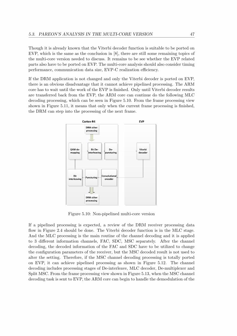
5.3. PAREON’S ANALYSIS IN THE MULTI-CORE VERSION 47
Though it is already known that the Viterbi decoder function is suitable to be ported onEVP, which is the same as the conclusion in [8], there are still some remaining topics ofthe multi-core version needed to discuss. It remains to be see whether the EVP relatedparts also have to be ported on EVP. The multi-core analysis should also consider timingperformance, communication data size, EVP-C realization efficiency.
If the DRM application is not changed and only the Viterbi decoder is ported on EVP,there is an obvious disadvantage that it cannot achieve pipelined processing. The ARMcore has to wait until the work of the EVP is finished. Only until Viterbi decoder resultsare transferred back from the EVP, the ARM core can continue do the following MLCdecoding processing, which can be seen in Figure 5.10. From the frame processing viewshown in Figure 5.11, it means that only when the current frame processing is finished,the DRM can step into the processing of the next frame.
Figure 5.10: Non-pipelined multi-core version
If a pipelined processing is expected, a review of the DRM receiver processing dataflow in Figure 2.4 should be done. The Viterbi decoder function is in the MLC stage.And the MLC processing is the main routine of the channel decoding and it is appliedto 3 different information channels, FAC, SDC, MSC separately. After the channeldecoding, the decoded information of the FAC and SDC have to be utilized to changethe configuration parameters of the receiver, but the MSC decoded result is not used toalter the setting. Therefore, if the MSC channel decoding processing is totally portedon EVP, it can achieve pipelined processing as shown in Figure 5.12. The channeldecoding includes processing stages of De-interleave, MLC decoder, De-multiplexer andSplit MSC. From the frame processing view shown in Figure 5.13, when the MSC channeldecoding task is sent to EVP, the ARM core can begin to handle the demodulation of the

48CHAPTER 5. ANALYSIS AND REALIZATION OF THE MULTI-CORE VERSION
Figure 5.11: Non-pipelined frame processing
next frame rather than waiting the end of the EVP task. Though the channel decodingstage of SDC and FAC still performs on ARM, it is still expected to provide a greatimprovement on the time performance since the MSC decoding workload is much higherthan FAC and SDC, for instance, in the benchmark, mytest1( MSC frame size is 6984,SDC is 630 and FAC is 72) and the MSC channel decoding takes more than 90% of thetotal channel decoding time.
Figure 5.12: Pipelined multi-core version
Porting the whole MSC channel decoding processing on EVP may deliver a high per-formance and pipelined processing. However, if considering the practical realization, itis not a good choice. There are a large amount of complex functions in De-interleave,MLC decoder, De-multiplexer and Split MSC and the only vectorizable function is theViterbi decoding of the MLC. And in the processing stage of De-interleave and someparts in MLC, the processing operates on floating point variables, which must be rewritefor EVP. In summary, it is hard to rewrite the whole code in MLC channel decodingin EVP-C to generate an efficient decoding implementation on EVP. The channel de-

5.3. PAREON’S ANALYSIS IN THE MULTI-CORE VERSION 49
Figure 5.13: Pipelined frame processing
coding’s slow execution on EVP may even eliminate the acceleration benefited by thepipelined processing. When the ARM core finishes the works of the next frame, it mayhave to wait for the EVP to finish the current frame’s decoding task.
An alternative option is to port the De-puncturing function into EVP, because thisprocessing function is closely related to the Viterbi decoder function. In this function,the BMs are achieved by calculating the soft-decision inputs, combining the puncturingtable. This function only takes a small amount of execution time, just 9.2% of the Viterbifunction based on the Cortex R4 optimized program’s result. However, the EVP-portingof the De-puncturing function will influence the size of data transferred from the ARMto the EVP. Thus there are two versions, namely the De-puncturing, Viterbi decoderEVP version and Viterbi decoder EVP version. We have to compare two versions in thesize of the communication data to be transferred from ARM to EVP and from EVP toARM.
The Vector Fabrics Tool, Pareon is used here to compare the communication of twoversions. This tool aims to help analyze the multi-core code. It is designed to find thedependency within program functions and give a guidance in optimizing the C/C++code on the multi-core architecture including Intel processors and ARM cores. Thistool is still under development, now it only supports the homogeneous multi-core systemwith shared memory. The functionality of support for the heterogeneous multi-corearchitecture and the simulation for the data transfer are not available yet. However, thecurrent version of Pareon can still be used to analyze the multi-core version.
The program needs to be recompiled by the Vector Fabrics compiler toolchain vfcc andvf++. Then the Pareon can analyze the code after the program’s execution. The GUIpresents a function distribution as shown in Figure 5.14 and the loop number is alsoshown in the GUI. In the source code, the function CViterbiDecoder::Decode onlycontains De-puncturing and Viterbi decoder and the Viterbi decoder processing is in
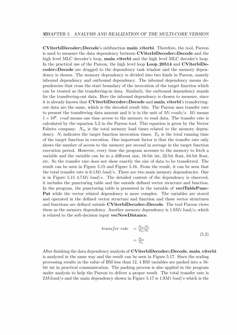
50CHAPTER 5. ANALYSIS AND REALIZATION OF THE MULTI-CORE VERSION
CViterbiDecoder::Decode’s subfunction main viterbi. Therefore, the tool, Pareonis used to measure the data dependency between CViterbiDecoder::Decode and thehigh level MLC decoder’s loop, main viterbi and the high level MLC decoder’s loop.In the practical use of the Pareon, the high level loop Loop 20514 and CViterbiDe-coder::Decode are dragged to the dependency task window and the memory depen-dency is chosen. The memory dependency is divided into two kinds in Pareon, namelyinbound dependency and outbound dependency. The inbound dependency means de-pendencies that cross the start boundary of the invocation of the target function whichcan be treated as the transferring-in data. Similarly, the outbound dependency standsfor the transferring-out data. Here the inbound dependency is chosen to measure, sinceit is already known that CViterbiDecoder::Decode and main viterbi’s transferring-out data are the same, which is the decoded result bits. The Pareon uses transfer rateto present the transferring data amount and it is in the unit of Mi reads/s. Mi means1 × 106. read means one time access to the memory to read data. The transfer rate iscalculated by the equation 5.2 in the Pareon tool. This equation is given by the VectorFabrics company. Nm is the total memory load times related to the memory depen-dency. Ni indicates the target function invocation times. Tti is the total running timeof the target function in execution. One important factor is that the transfer rate onlyshows the number of access to the memory per second in average in the target functionexecution period. However, every time the program accesses to the memory to fetch avariable and the variable can be in a different size, 16-bit int, 32-bit float, 64-bit float,etc. So the transfer rate does not show exactly the size of data to be transferred. Theresult can be seen in Figure 5.15 and Figure 5.16. From the result, it can be seen thatthe total transfer rate is 6.1Mi load/s. There are two main memory dependencies. Oneis in Figure 5.15 4.7Mi load/s. The detailed content of the dependency is observed,it includes the puncturing table and the outside defined vector structure and function.In the program, the puncturing table is presented in the variable of veciTablePunc-Pat while the vector related dependency is more complex. The variables are storedand operated in the defined vector structure and function and these vector structuresand functions are defined outside CViterbiDecoder::Decode. The tool Pareon viewsthem as the memory dependency. Another memory dependency is 1.9Mi load/s, whichis related to the soft-decision input vecNewDistance.
transfer rate = Nm/Ni
Tti/Ni
= NmTti
(5.2)
After finishing the data dependency analysis of CViterbiDecoder::Decode, main viterbiis analyzed in the same way and the result can be seen in Figure 5.17. Since the scalingprocessing results in the value of BM less than 12, 4 BM variables are packed into a 16-bit int in practical communication. The packing process is also applied in the programunder analysis to help the Pareon to deliver a proper result. The total transfer rate is2Miload/s and the main dependency shown in Figure 5.17 is 1.9Mi load/s which is the
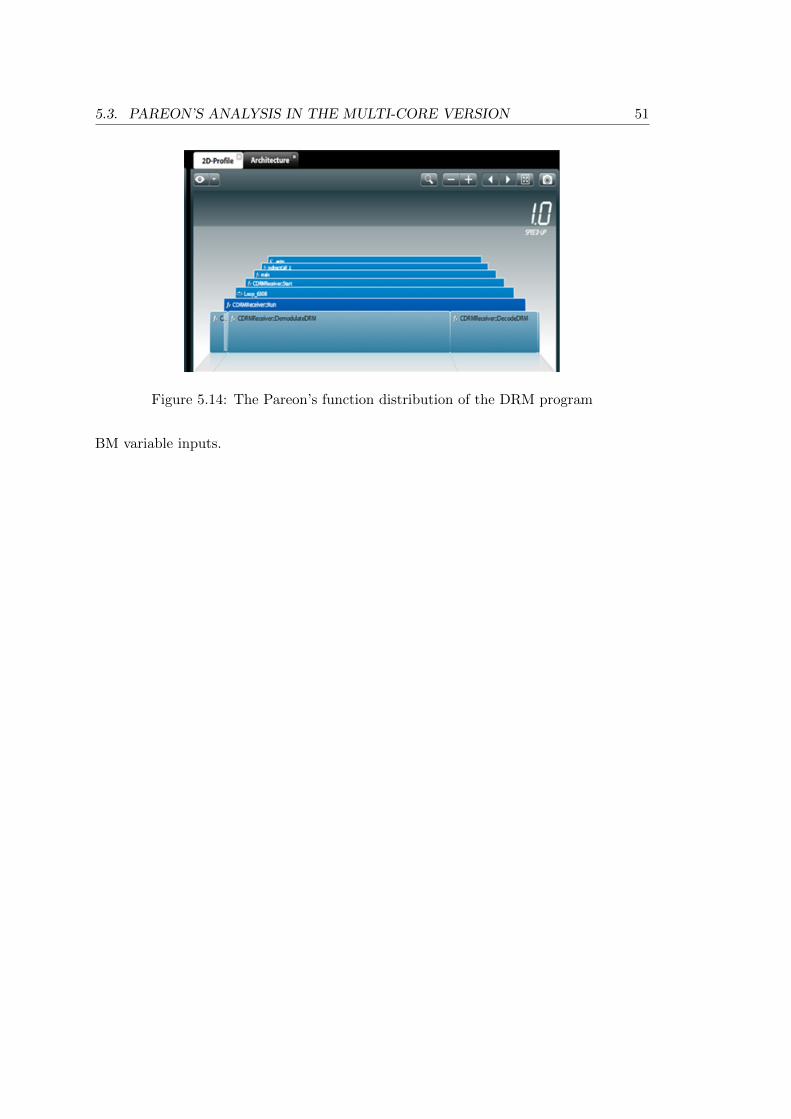
5.3. PAREON’S ANALYSIS IN THE MULTI-CORE VERSION 51
Figure 5.14: The Pareon’s function distribution of the DRM program
BM variable inputs.

52CHAPTER 5. ANALYSIS AND REALIZATION OF THE MULTI-CORE VERSION
Figure 5.15: CViterbiDecoder::Decode inbound memory dependency 1

5.3. PAREON’S ANALYSIS IN THE MULTI-CORE VERSION 53
Figure 5.16: CViterbiDecoder::Decode inbound memory dependency 2

54CHAPTER 5. ANALYSIS AND REALIZATION OF THE MULTI-CORE VERSION
Figure 5.17: main viterbi inbound memory dependency

5.3. PAREON’S ANALYSIS IN THE MULTI-CORE VERSION 55
From the total transfer rate view, the function CViterbiDecoder::Decode has abigger data dependency. If the exactly communication data size needs to be ana-lyzed, the equation 5.3 is used. #memory access per second is the so-called trans-fer rate in the Pareon. CViterbiDecoder::Decode has a higher transfer rate thanmain viterbi as it is shown before. Ttotalinvocation of CViterbiDecoder::Decode isobviously larger than that of main viterbi. Because main viterbi is a subfunction ofCViterbiDecoder::Decode. For size of each memory access, the variable neededto read in CViterbiDecoder::Decode is 32-bit float. However, in main viterbithe variable size is smaller, 16-bit integer. Thus considering all the three parameters,#memory access per second, Ttotalinvocation, and size of each memory access in theequation, it can be concluded that the size of data needed to be transferred in CViter-biDecoder::Decode is bigger than main viterbi.
transfer data size = #memory access per second× Ttotalinvocation × size of each memory access(5.3)
To confirm the result obtaining from Pareon, the size of the data needed to be transferredis calculated. For n step Viterbi decoder, the data size transferred from the ARM to EVPin two version is presented in Table 5.3. For main viterbi, n step needs 8×n BM inputs.4 BM variables are packed into a 16-bit int which is 2 byte. Thus n× 4 byte needs to betransfered. In CViterbiDecoder::Decode version, the data needed to be transferred,include soft-decision input vecNewDistance and puncturing table. The vector relateddependency is not considered here, because in the practical implementation, the vectorstructure and function can also be located in the EVP. Puncturing table size calculationis simple, n × 4 byte. However, vecNewDistance is much more complex because ofthe various puncturing patterns. In different puncturing patterns, there can be 2 soft-decision inputs, 4 soft-decision inputs, 6 soft-decision inputs or 8 soft-decision inputsinvolved in calculating the BMs of one step trellis construction. Each soft-decision inputis in the variable of 32-bit float and a, b, c, d stands for number of steps punctured incertain puncturing pattern. Thus the equation shown in 5.3 can be obtained. a × 8 +b× 16 + c× 24 + d× 32 + n× 4 is obviously larger than n× 4, therefore transferring indata size of main viterbi is smaller than that of CViterbiDecoder::Decode, whichis consist with result obtained from Pareon.
Thus after analyzing the results from the Pareon tool, it is apparent that porting theDe-puncturing function into EVP is not wise.
Table 5.3: Transferring in data size of two versionmain viterbi CViterbiDecoder::Deocde
n× 4 byte a×8+b×16+c×24+d×32+n×4 byte(a+b+ c+ d = n)
For other functions in MLC, they only take a smaller part of execution time and these

56CHAPTER 5. ANALYSIS AND REALIZATION OF THE MULTI-CORE VERSION
functions are either hard to be vectorized or are implemented using floating-point vari-able. It is not wise to port them too.
In conclusion, it is not chosen to port the whole channel decoding process of MSC on EVPbecause of its low efficiency in EVP-C realization and its possible bad time performanceon EVP which eliminates the speed’s improvement benefiting from pipelined processing.The De-puncturing function is also not ported on EVP, since the Pareon shows thatthis multi-core version leads to a larger amount of data needed to be transferred fromARM to EVP. Finally it is determined that the Viterbi decoder function is ported onEVP.
A coarse calculation of this multi-core version’s performance is done here. The processingtime of each frame can be obtained from Figure 4.7. The longest processing time ofgenerating a single service frame is 634 ms (3rd frame and 9th frame), except the firstframe. In the multi-core version, if the 3rd and 9rd frame processing time can be reducedto less than 400 ms, thus all the frame processing time will be less than 400 ms and thereceiver can deliver a real-time service. 45% of the 634 ms processing time, is contributedby the Viterbi decoder function, which is 289.35 ms. In the multi-core version, theViterbi decoder function execution time is decreased. If the processing time is expectedto be less than 400 ms, the Viterbi decoding process on EVP should be less than 46.35 mswhich is presented in Figure 5.18. Therefore, if the communication overhead is not takeninto consideration, the EVP must deliver a Viterbi decoding processing at least 6.24X(6.24 = 289.35
46.35 ) faster than the ARM version in order to achieve a real-time service. Thecommunication overhead is discussed in section 6.1.
In the next section, the detailed Viterbi decoder function’s realization on EVP is dis-cussed.
5.4 Achieving the Viterbi decoder on EVP
On account of the result from section 5.3, the Viterbi decoder of the DRM receiver isported on EVP.
In the original Viterbi decoder, the frame based trace back is used. It is reasonable sincethe target platform of the Dream DRM receiver is on PC which has a fast processingspeed and a large amount of memory available. Therefore, the PC version ignores thedemands for speeding up or reduction of the memory, but mainly focuses on increasingthe accuracy. The original Viterbi decoder also ignores overflow, since the PC can use64-bit double or 32-bit float which provides a bigger range. Considering porting on EVP,these two mentioned settings have to be discussed whether they need to be changed whenthe decoder is ported to the EVP. The EVP processor runs at 419 MHz and the parallelprocessing ability (SIMD) already gives an extremely increase in processing speed, itis not necessary to change the trace back method to speed up. For memory size, acalculation is needed. For the max step decoder, 4206 trellis steps are achieved and
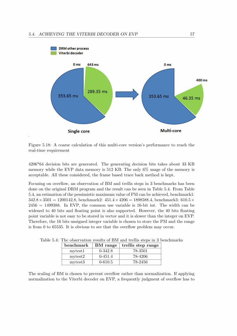
5.4. ACHIEVING THE VITERBI DECODER ON EVP 57
Figure 5.18: A coarse calculation of this multi-core version’s performance to reach thereal-time requirement
4206*64 decision bits are generated. The generating decision bits takes about 33 KBmemory while the EVP data memory is 512 KB. The only 6% usage of the memory isacceptable. All these considered, the frame based trace back method is kept.
Focusing on overflow, an observation of BM and trellis steps in 3 benchmarks has beendone on the original DRM program and the result can be seen in Table 5.4. From Table5.4, an estimation of the pessimistic maximum value of PM can be achieved, benchmark1:342.8×3501 = 1200142.8, benchmark2: 451.4×4206 = 1898588.4, benchmark3: 610.5×2456 = 1499388. In EVP, the common use variable is 16-bit int. The width can bewidened to 40 bits and floating point is also supported. However, the 40 bits floatingpoint variable is not easy to be stored in vector and it is slower than the integer on EVP.Therefore, the 16 bits unsigned integer variable is chosen to store the PM and the rangeis from 0 to 65535. It is obvious to see that the overflow problem may occur.
Table 5.4: The observation results of BM and trellis steps in 3 benchmarksbenchmark BM range trellis step range
mytest1 0-342.8 78-3501
mytest2 0-451.4 78-4206
mytest3 0-610.5 78-2456
The scaling of BM is chosen to prevent overflow rather than normalization. If applyingnormalization to the Viterbi decoder on EVP, a frequently judgment of overflow has to
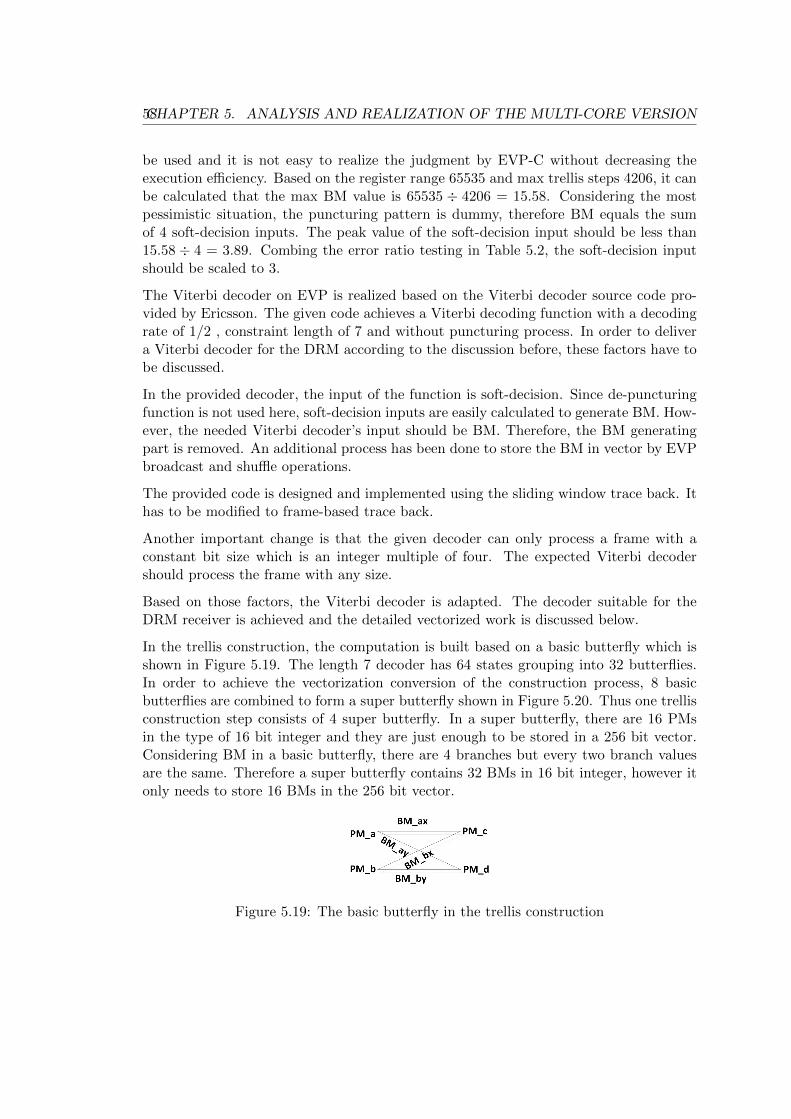
58CHAPTER 5. ANALYSIS AND REALIZATION OF THE MULTI-CORE VERSION
be used and it is not easy to realize the judgment by EVP-C without decreasing theexecution efficiency. Based on the register range 65535 and max trellis steps 4206, it canbe calculated that the max BM value is 65535 ÷ 4206 = 15.58. Considering the mostpessimistic situation, the puncturing pattern is dummy, therefore BM equals the sumof 4 soft-decision inputs. The peak value of the soft-decision input should be less than15.58 ÷ 4 = 3.89. Combing the error ratio testing in Table 5.2, the soft-decision inputshould be scaled to 3.
The Viterbi decoder on EVP is realized based on the Viterbi decoder source code pro-vided by Ericsson. The given code achieves a Viterbi decoding function with a decodingrate of 1/2 , constraint length of 7 and without puncturing process. In order to delivera Viterbi decoder for the DRM according to the discussion before, these factors have tobe discussed.
In the provided decoder, the input of the function is soft-decision. Since de-puncturingfunction is not used here, soft-decision inputs are easily calculated to generate BM. How-ever, the needed Viterbi decoder’s input should be BM. Therefore, the BM generatingpart is removed. An additional process has been done to store the BM in vector by EVPbroadcast and shuffle operations.
The provided code is designed and implemented using the sliding window trace back. Ithas to be modified to frame-based trace back.
Another important change is that the given decoder can only process a frame with aconstant bit size which is an integer multiple of four. The expected Viterbi decodershould process the frame with any size.
Based on those factors, the Viterbi decoder is adapted. The decoder suitable for theDRM receiver is achieved and the detailed vectorized work is discussed below.
In the trellis construction, the computation is built based on a basic butterfly which isshown in Figure 5.19. The length 7 decoder has 64 states grouping into 32 butterflies.In order to achieve the vectorization conversion of the construction process, 8 basicbutterflies are combined to form a super butterfly shown in Figure 5.20. Thus one trellisconstruction step consists of 4 super butterfly. In a super butterfly, there are 16 PMsin the type of 16 bit integer and they are just enough to be stored in a 256 bit vector.Considering BM in a basic butterfly, there are 4 branches but every two branch valuesare the same. Therefore a super butterfly contains 32 BMs in 16 bit integer, however itonly needs to store 16 BMs in the 256 bit vector.
Figure 5.19: The basic butterfly in the trellis construction

5.4. ACHIEVING THE VITERBI DECODER ON EVP 59
Figure 5.20: The super butterfly in the trellis construction
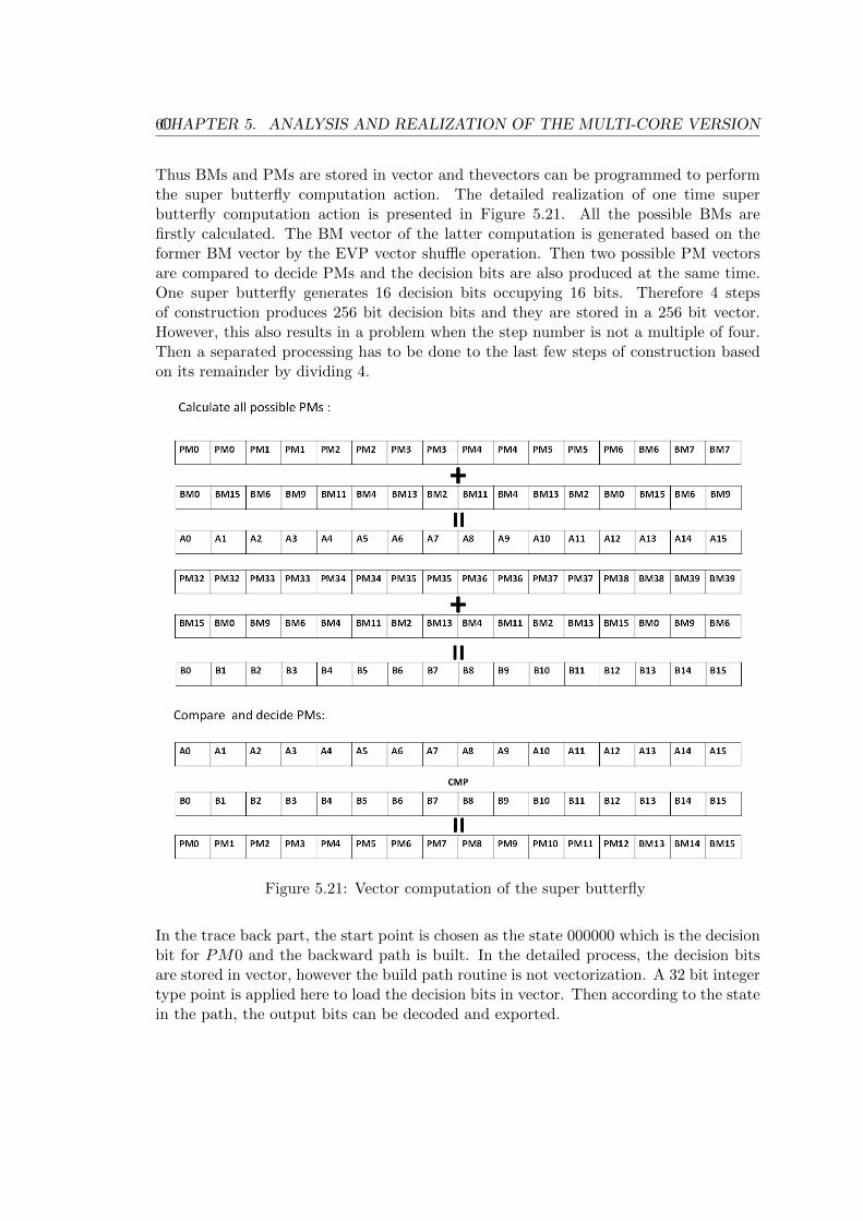
60CHAPTER 5. ANALYSIS AND REALIZATION OF THE MULTI-CORE VERSION
Thus BMs and PMs are stored in vector and thevectors can be programmed to performthe super butterfly computation action. The detailed realization of one time superbutterfly computation action is presented in Figure 5.21. All the possible BMs arefirstly calculated. The BM vector of the latter computation is generated based on theformer BM vector by the EVP vector shuffle operation. Then two possible PM vectorsare compared to decide PMs and the decision bits are also produced at the same time.One super butterfly generates 16 decision bits occupying 16 bits. Therefore 4 stepsof construction produces 256 bit decision bits and they are stored in a 256 bit vector.However, this also results in a problem when the step number is not a multiple of four.Then a separated processing has to be done to the last few steps of construction basedon its remainder by dividing 4.
Figure 5.21: Vector computation of the super butterfly
In the trace back part, the start point is chosen as the state 000000 which is the decisionbit for PM0 and the backward path is built. In the detailed process, the decision bitsare stored in vector, however the build path routine is not vectorization. A 32 bit integertype point is applied here to load the decision bits in vector. Then according to the statein the path, the output bits can be decoded and exported.
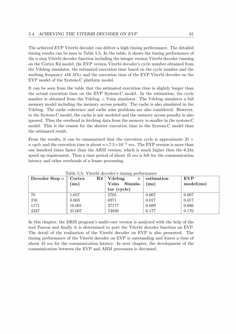
5.4. ACHIEVING THE VITERBI DECODER ON EVP 61
The achieved EVP Viterbi decoder can deliver a high timing performance. The detailedtiming results can be seen in Table 5.5. In the table, it shows the timing performance ofthe n step Viterbi decoder function including the integer version Viterbi decoder runningon the Cortex R4 model, rhe EVP version Viterbi decoder’s cycle number obtained fromthe Vdebug simulator, the estimated execution time based on the cycle number and theworking frequency 416 Mhz and the execution time of the EVP Viterbi decoder on theEVP model of the System-C platform model.
It can be seen from the table that the estimated execution time is slightly longer thanthe actual execution time on the EVP System-C model. In the estimation, the cyclenumber is obtained from the Vdebug + Vsim simulator. The Vdebug simulates a fullmemory model including the memory access penalty. The cache is also simulated in theVdebug. The cache coherence and cache miss problems are also considered. However,in the System-C model, the cache is not modeled and the memory access penalty is alsoignored. Thus the overhead in fetching data from the memory is smaller in the system-Cmodel. This is the reason for the shorter execution time in the System-C model thanthe estimated result.
From the results, it can be summarized that the execution cycle is approximate 31 ×n cycle and the execution time is about n×7.5×10⁻⁵ ms. The EVP version is more thanone hundred times faster than the ARM version, which is much higher then the 6.24xspeed up requirement. Thus a time period of about 45 ms is left for the communicationlatency and other overheads of a frame processing.
Table 5.5: Viterbi decoder’s timing performanceDecoder Step n Cortex R4
(ms)Vdebug +Vsim Simula-tor (cycle)
estimation(ms)
EVPmodel(ms)
78 1.657 2705 0.007 0.007216 3.003 6971 0.017 0.0171171 16.001 37177 0.089 0.0862337 25.007 73839 0.177 0.170
In this chapter, the DRM program’s multi-core version is analyzed with the help of thetool Pareon and finally it is determined to port the Viterbi decoder function on EVP.The detail of the realization of the Viterbi decoder on EVP is also presented. Thetiming performance of the Viterbi decoder on EVP is outstanding and leaves a time ofabout 45 ms for the communication latency. In next chapter, the development of thecommunication between the EVP and ARM processors is discussed.

62CHAPTER 5. ANALYSIS AND REALIZATION OF THE MULTI-CORE VERSION

Chapter 6
Communication between theARM and the EVP
In this chapter, the working principle of the DMA controller and its detailed configura-tion is introduced in Section 6.1. Afterwards, the design of the communication betweenthe EVP core and the ARM processor is presented in Section 6.2.
6.1 Programming on the DMA
The DMA controller on the target platform is AXI DMAC CORE V2. It is an AXI buscontroller with three 64-bit master ports and one 32-bit slave port which efficiently movesdata from one location to another. Since the DMA launches communications insteadof the processor, the control task is offloaded from the processor and the processor canoperate other tasks in parallel with DMA’s communication tasks.
The architecture of the DMA implementation on the target platform is presented in Fig-ure 6.1. The EVP and ARM processors can access the DMA parameter register throughthe slave port to control the configuration of the transfer including source address, des-tination address, transferring data size, etc. According to the setting, the 3 master portscan access the source and destination components to execute the data transfer. FromFigure 6.1, it can be seen that the slave port is connected to the APB bus rather thanAXI bus. As it is discussed in section 3.3, the AXI bus delivers a burst-based, pipelineddata transfer. However, the written transfer to the DMA register is simple data transferrather than the burst transfer because scalar variables needs to be transferred to variousregisters in scattering addresses in the DMA configuration. Thus APB is a suitablebus which reduces interface complexity and lowers power consumption and provides anon-pipelined data transfer. A bridge is located between the APB and AXI to serve asa frequency and transfer protocol convertor. For the purpose of energy saving, the APBbus works at a much lower frequency than AXI. Since the DMA configuration registers

64 CHAPTER 6. COMMUNICATION BETWEEN THE ARM AND THE EVP
are in the data width of 32 bits, a data width conversion from 64 bits to 32 bits isnecessary.
Figure 6.1: The architecture of DMA implementation on the target platform
The DMA controller can handle 4 kinds of transfer classified by source and destina-tion type, namely memory-to-memory, peripheral-to-memory, memory-to-peripheral andperipheral-to-peripheral. In this DRM implementation, the DMA only involves in thememory-to-memory transfer to achieve the communication between the EVP and ARMprocessor. The memory of the EVP is embedded in the EVP processor and memory ofthe Cortex R4 processor is external DDR RAM0 and RAM1. The DMA launches thedata transfer between the EVP memory and the DDR RAM.
The data flow of DMA memory-to-memory data transfer can be seen in Figure 6.2. Themaster read port0 reads data from the memory through AXI bus. The data is stored inthe FIFO buffer of DMA. When the data stored in the FIFO is enough to start a transfertask launched by the master write port, the data in the buffer is written to the destinationmemory through the AXI bus. The byte size of a single transfer task is decided by thevalue in PLEN (Packet Length) register which indicates the maximum number of bytesthat will be transferred per task. When the transfer task ends, the DMA processes anarbiter operation to choose the next processing channel. If the same channel is chosento continue processing, a similar transfer process is repeated. However, the arbitrationprocess between transfer tasks will add an additional overhead to the transfer. Thusthe data in the size of Packet Length is transferred from one memory to another. Thisprocess is called a transfer task and multi transfer tasks compose a DMA transferringjob. The max data size of a DMA transferring job is 0.5 MB.
In the practical use of the DMA controller, the ARM Cortex R4 processor is programmed
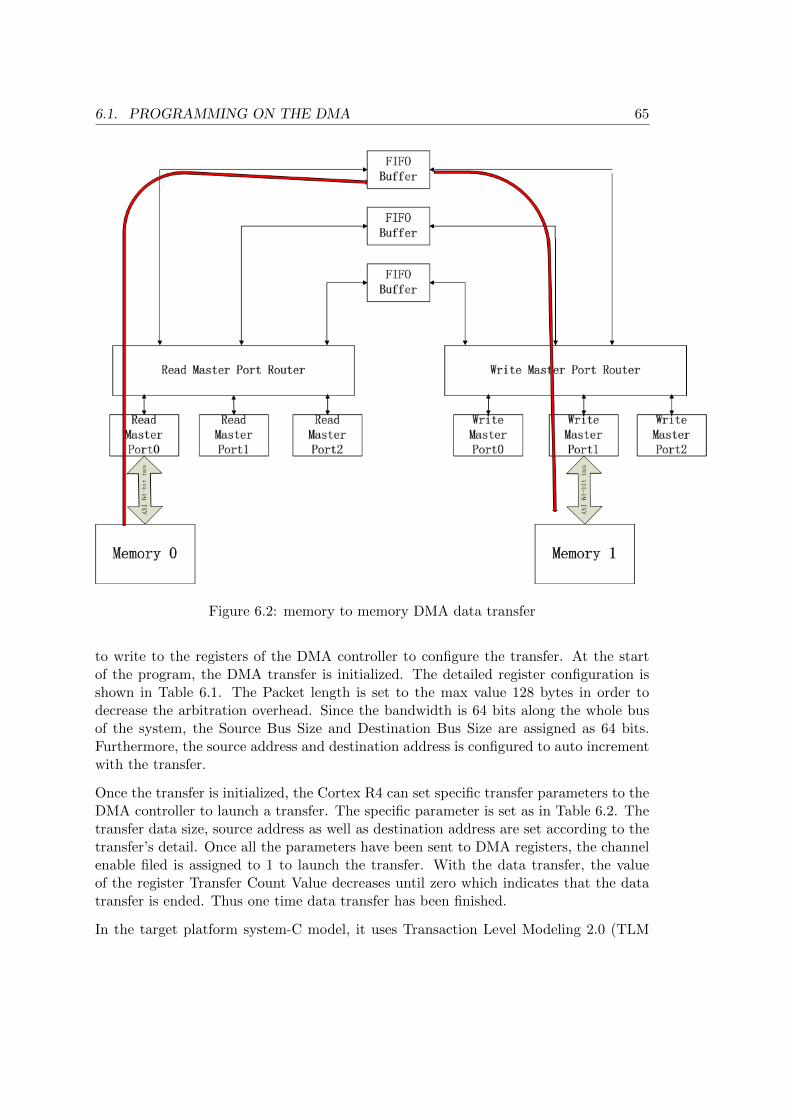
6.1. PROGRAMMING ON THE DMA 65
Figure 6.2: memory to memory DMA data transfer
to write to the registers of the DMA controller to configure the transfer. At the startof the program, the DMA transfer is initialized. The detailed register configuration isshown in Table 6.1. The Packet length is set to the max value 128 bytes in order todecrease the arbitration overhead. Since the bandwidth is 64 bits along the whole busof the system, the Source Bus Size and Destination Bus Size are assigned as 64 bits.Furthermore, the source address and destination address is configured to auto incrementwith the transfer.
Once the transfer is initialized, the Cortex R4 can set specific transfer parameters to theDMA controller to launch a transfer. The specific parameter is set as in Table 6.2. Thetransfer data size, source address as well as destination address are set according to thetransfer’s detail. Once all the parameters have been sent to DMA registers, the channelenable filed is assigned to 1 to launch the transfer. With the data transfer, the valueof the register Transfer Count Value decreases until zero which indicates that the datatransfer is ended. Thus one time data transfer has been finished.
In the target platform system-C model, it uses Transaction Level Modeling 2.0 (TLM

66 CHAPTER 6. COMMUNICATION BETWEEN THE ARM AND THE EVP
Table 6.1: The detailed register configuration of DMA transfer initializationField name Setting
Request Mode Memory to Memory
Master Mode master 0 read, master 1 write
Packet Length 128 byte
Source Bus Size 64 bit
Destination Bus Size 64 bit
Source Address Increment Increment by Source Bus Size
Destination Address In-crement
Increment by Destination Bus Size
Table 6.2: The detailed register configuration of a specific transferField name Setting
Transfer Count Value communication data size in byte
Transfer Count Enable count down
Source Address source address in the global memory map
Destination Address destination address in the global memory map
Channel Enable for chan-nel 1
enable
2.0) to model the communication. However in order to reduce the model’s complexity,the model does not simulate the burst transfer time of the communication controlled byDMA. In the DMA model-C code, the function MasterReadFormatTLM2 is calledto process the master port’s reading from the source component. In the function, theblocking transport call’s delay is set zero. It is the same case in the function Mas-terWriteFormatTLM2 which process the master port’s writing to the destinationcomponent. Thus the latency in the burst transfer is zero in the model. An additionaltransfer latency should be taken into consideration in the profile report in the multi-coreDRM software on the target model.
6.2 Communication between the ARM and EVP with theDMA
In the last section, the data transfer controlled by the DMA controller has been achieved.Based on the DMA data transfer, the communication protocol between the EVP andARM cores implementing in the DRM receiver multi-core version, is presented in thissection.
Since the EVP core is idle during most of the execution time, it is set in the low powermode when it is not waked up by the external interrupt sent by the ARM core. Once

6.2. COMMUNICATION BETWEEN THE ARM AND EVP WITH THE DMA 67
the EVP task is finished, the EVP will interrupt itself to turn to the low power sleepmode.
The detailed EVP code of the state switching and response to the interrupt is based onthe EVP example implementation Sound Machine. Three interrupt requests, namelyWakeUp, Sleep and Exit and one semaphore event, CONTINUE are defined torealize the state switching and they are presented in Figure 6.3. In the run state, itprocesses the decoding task and switches into the sleep mode if it receives a Sleep IRQ.In the sleep mode, it uses the EVP function evp wait() to wait for a semaphore event.Once WakeUp IRQ occurs, it calls for the semaphores event, CONTINUE to triggerthe EVP into the run state. The state, run and sleep both can switch into the exit stateto completely end the EVP’s execution.
Figure 6.3: The design of EVP state switching
However, in the practical implementation of the sleep mode on the EVP model, we haveto prevent an error occurring that the EVP core stalls forever when it steps into thesleep mode. When there is a load started before a wait instruction, the stall can happenthat the read data is returned after the core clock has been switched off by the waitinstruction. It can be solved by adding a evp dsb() function before evp wait() toinsert a data synchronization boundary instruction that forces the memory read to befinished before the wait instruction is executed.
The components, ARM, EVP and DMA involved in the communication need to syn-chronize with each other to inform their own working progress. The detail of the com-munication design is presented in Figure 6.4.
From the sequence diagram, it can be seen that the ARM core firstly initiates a DMAtransfer to send the Viterbi decoding input data to the EVP. After configuration, theDMA starts the burst transfer. The ARM core is informed of the transfer’s ending bychecking the transfer status register of the DMA. When the transfer ends, the ARM coresends request to the DMA to clear the transfer status register to prepare for the next

68 CHAPTER 6. COMMUNICATION BETWEEN THE ARM AND THE EVP
time transfer.
Once the Viterbi decoding input data is already available in the EVP memory, the ARMcore can send the interrupt to the EVP to wake it up. Then the EVP starts the decodingtask. When the task is finished, it changes the flag to show that and turns into the sleepmode. At the same time, the ARM core checks for the EVP’s flag to obtain the progressof the EVP task . Once being informed of the finish of the decoding task , the ARM coreinitiates a DMA transfer to read the Viterbi decoding results into the ARM’s memoryin the same way as the write to the EVP memory.
There is also a pack work implemented in the data needed to be transferred to decreasethe communication data size. As it is mentioned in Section 5.3, the data transferredfrom the ARM core to the EVP can be packed. Each variable’s value is less than 12which can be presented by a register of 4 bits, therefore, four variables can be packed ina 16-bit short int. The decoding result which need to be transferred from the EVP tothe ARM is binary bit and each only occupies 1 bit. Thus 16 variables can be packedin a 2-byte int. There are unpacking routines in both the ARM and EVP sides in orderto use the data.

6.2. COMMUNICATION BETWEEN THE ARM AND EVP WITH THE DMA 69
Figure 6.4: The design of the communication between the ARM and EVP
70 CHAPTER 6. COMMUNICATION BETWEEN THE ARM AND THE EVP
After finishing the detailed development of communication, the Multicore Communica-tions API (MCAPI) is used to modularize the multi-core communication. The detailedMCAPI design is presented in Appendix B.
In this chapter, the development and design of the communication between the EVP anARM processors is presented. A estimation of the multi-core performance can be donebased on the communication design and the timing performance on EVP. The processof the estimation can be seen in next chapter.

Chapter 7
Multi-core version Performance’sEstimation and Verification
This chapter consists of two parts. One is to estimate the multi-core timing performancein section 7.1. Another in section 7.2 is to present the profile report on the platformmodel and the actual performance is compared with the estimation.
7.1 Estimation of the Multi-core version Performance
Combining the design of the multi-core software and communication settings in previouschapters, a multi-core version performance can be estimated here. The processing timeof each frame in benchmark1 is estimated using equation 7.1. The estimation does notinvolve in the first frame, since it will not influence the real-time service. TDRM is theexecution time of the DRM other code on ARM. TDMA indicates the time spent in theDMA configuration for a specific transfer . The time resulted from synchronization isin Tsynchronization. The burst transfer latency is Tcommunication. At last, TEV P is theViterbi decoding processing time on EVP.
Tframe = TDRM + TDMA + Tsynchronization + Tcommunication + TEV P (7.1)
TDRM is easy to obtain by using the Cortex R4 results in Figure 4.7 and the Viterbidecoder’s 45% contribution. The processing time of each frame is multiplied by 55% toget the DRM other processing’s execution time and the result is in Table 7.1
For the calculation of TDMA, Tsynchronization, Tcommunication and TEV P , the frame decod-ing workload should be known in each frame. In the bechmark1, the 3-level MLC decoderis applied for the MSC in the transmitter. And the number of source information bits ineach stream are 1171, 2337 and 3501 respectively. Since the iterative parameter is 2 in

72CHAPTER 7. MULTI-CORE VERSION PERFORMANCE’S ESTIMATION AND
VERIFICATION
Table 7.1: TDRM from frame2 to frame 11 in benchmark1FrameID
2 3 4 5 6 7 8 9 10 11
TDRM ms 310.2 348.7 306.9 305.8 345.4 306.35 308.55 348.7 305.8 306.9
the MLC decoder of the receiver, thus there are two 1171-step, two 2237-step and two3501-step Viterbi decoding routines in the process of decoding a MSC frame. The 2-levelMLC is applied to the SDC frame and the number of source bits in each stream are 216,426 respectively. Thus there are two 216-step, two 426-step Viterbi decoding routines inthe process of decoding a SDC frame. In FAC, the 1-level MLC is used and the numberof source bits in the stream is 78. Though the iterative loop is 2, it is not suitable for the1-level MLC decoder. There is only one 78-step Viterbi decoding routine in the decodingone FAC frame. In a super frame, the first frame contains one MSC, one SDC frame andone FAC frame and the other two frame only contain one MSC and one FAC frame. Fora larger decoding workload of the frame, the work consists of two 1171-step, two 2337-step and two 3501-step, two 216-step, two 426-step and one 78-step Viterbi decodingroutines. For a smaller workload of the frame, there are two 1171-step, two 2337-stepand two 3501-step and one 78-step Viterbi decoding works. The detailed workload ineach frame can be seen in Table 7.2. The number of Viterbi decoding routines in oneframe is shown in 7.1. The trends of TDMA, Tsynchronization, Tcommunication and TEV Pare the same as that of #V iterbi routines in each frame.
Table 7.2: Workload from frame2 to frame 11 in benchmark1FrameID
2 3 4 5 6 7 8 9 10 11
FrameWorkLoad
FAC+MSC
FAC+SDC+MSC
FAC+MSC
FAC+MSC
FAC+SDC+MSC
FAC+MSC
FAC+MSC
FAC+SDC+MSC
FAC+MSC
FAC+MSC
In TDMA, the ARM core sends source address, destination address, transfer size as wellas enable signal to the DMA controller. These values are firstly calculated in the ARMprogram and then copied to the DMA address by memcpy. Each memcpy instructiontakes 0.0002 ms. It is measured by the analysis function of the Synopsys tool. Fourmemcpys are called in the configuration. Thus one DMA configuration takes about0.0008 ms. The DMA register has to be configured twice in each Viterbi process onEVP for data transferring in and data transferring out. For 2nd frame, it has to decodeone MSC, one FAC and seven Viterbi decoder functions are called. Therefore, TDMA
equals 0.0008 × 2 × 7 ms. The rest frames can be calculated in the same way and theresult can be seen in Table 7.3.
Tsynchronization indicates the time spent in the synchronization between different compo-

7.1. ESTIMATION OF THE MULTI-CORE VERSION PERFORMANCE 73
Figure 7.1: The number of Viterbi decoding routines in each frame
Table 7.3: TDMA from frame2 to frame 11 in benchmark1FrameID
2 3 4 5 6 7 8 9 10 11
TDMA ms 0.011 0.018 0.011 0.011 0.018 0.011 0.011 0.018 0.011 0.011
nents. The DMA has to inform the ARM core of the data transfer’s ending or the statusregister’s clear. The ARM processor requests the EVP to start work and the EVP hasto inform the ARM core that the Viterbi processing is finished. It is hard to predict onthis value, here we assume that each synchronization process takes 0.001 ms which isabout 400 ARM cycles. There are 6 synchronization processes in each Viterbi decoding.Thus Tsynchronization can be calculated and the results are in Table 7.4.
Table 7.4: Tsynchronization from frame2 to frame 11 in benchmark1
FrameID
2 3 4 5 6 7 8 9 10 11
Tsyn ms 0.042 0.066 0.042 0.042 0.066 0.042 0.042 0.066 0.042 0.042
Based on the Viterbi decoding input and output data size and hardware details, thecommunication latency Tcommunication is estimated as following.
Firstly, a coarse calculation excluding the burst transfer’s details and the DMA control, isachieved to measure the communication time. For a n step Viterbi decoding, combiningwith the data package condition, the data size from the ARM core to the EVP core isn × 4 byte and from the EVP core to the ARM core is d n16e × 2 byte. For instance,the processing of the 2nd frame, contains two 1171-step, two 2337-step and two 3501-step and one 78-step Viterbi decoding and each Viterbi processing’s transferring in and
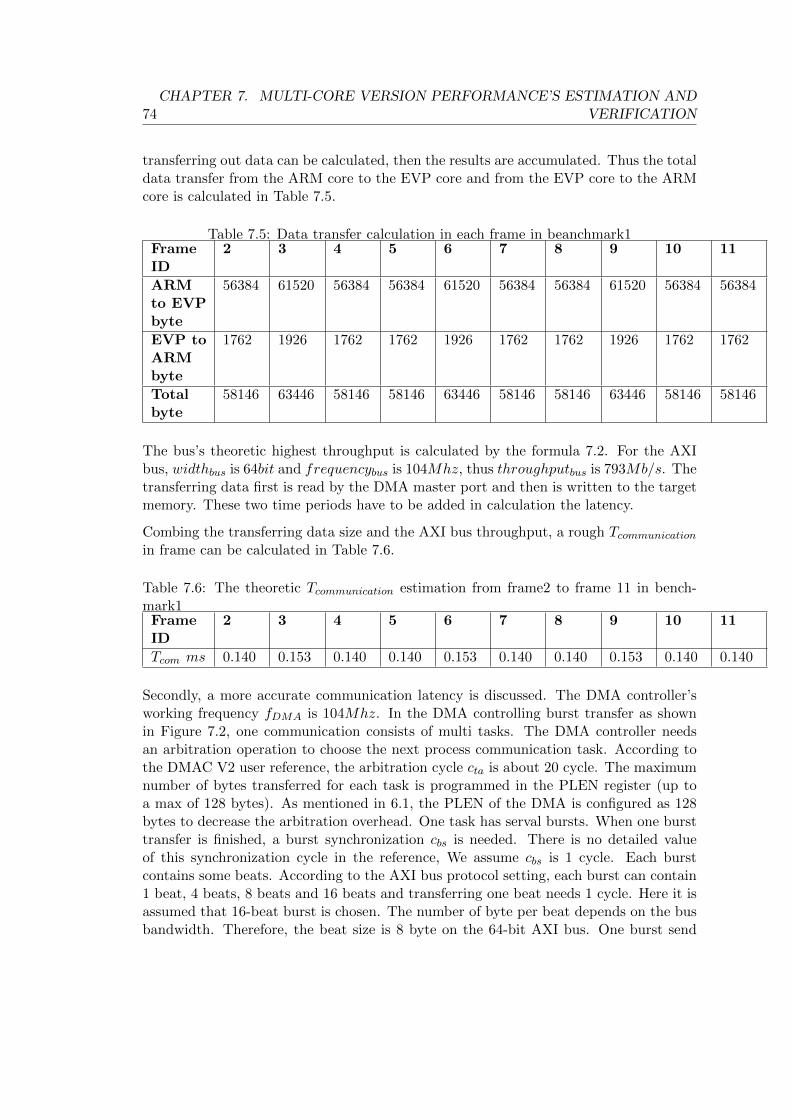
74CHAPTER 7. MULTI-CORE VERSION PERFORMANCE’S ESTIMATION AND
VERIFICATION
transferring out data can be calculated, then the results are accumulated. Thus the totaldata transfer from the ARM core to the EVP core and from the EVP core to the ARMcore is calculated in Table 7.5.
Table 7.5: Data transfer calculation in each frame in beanchmark1FrameID
2 3 4 5 6 7 8 9 10 11
ARMto EVPbyte
56384 61520 56384 56384 61520 56384 56384 61520 56384 56384
EVP toARMbyte
1762 1926 1762 1762 1926 1762 1762 1926 1762 1762
Totalbyte
58146 63446 58146 58146 63446 58146 58146 63446 58146 58146
The bus’s theoretic highest throughput is calculated by the formula 7.2. For the AXIbus, widthbus is 64bit and frequencybus is 104Mhz, thus throughputbus is 793Mb/s. Thetransferring data first is read by the DMA master port and then is written to the targetmemory. These two time periods have to be added in calculation the latency.
Combing the transferring data size and the AXI bus throughput, a rough Tcommunicationin frame can be calculated in Table 7.6.
Table 7.6: The theoretic Tcommunication estimation from frame2 to frame 11 in bench-mark1FrameID
2 3 4 5 6 7 8 9 10 11
Tcom ms 0.140 0.153 0.140 0.140 0.153 0.140 0.140 0.153 0.140 0.140
Secondly, a more accurate communication latency is discussed. The DMA controller’sworking frequency fDMA is 104Mhz. In the DMA controlling burst transfer as shownin Figure 7.2, one communication consists of multi tasks. The DMA controller needsan arbitration operation to choose the next process communication task. According tothe DMAC V2 user reference, the arbitration cycle cta is about 20 cycle. The maximumnumber of bytes transferred for each task is programmed in the PLEN register (up toa max of 128 bytes). As mentioned in 6.1, the PLEN of the DMA is configured as 128bytes to decrease the arbitration overhead. One task has serval bursts. When one bursttransfer is finished, a burst synchronization cbs is needed. There is no detailed valueof this synchronization cycle in the reference, We assume cbs is 1 cycle. Each burstcontains some beats. According to the AXI bus protocol setting, each burst can contain1 beat, 4 beats, 8 beats and 16 beats and transferring one beat needs 1 cycle. Here it isassumed that 16-beat burst is chosen. The number of byte per beat depends on the busbandwidth. Therefore, the beat size is 8 byte on the 64-bit AXI bus. One burst send

7.1. ESTIMATION OF THE MULTI-CORE VERSION PERFORMANCE 75
data of 128 byte, so a communication task consists of 1 burst. Furthermore, a initiallatency cil has to be added before launch one communication job and it is 25 cyclesaccording to the user reference.
throughputbus = widthbus × frequencybus (7.2)
Figure 7.2: The structure of the DMA burst communication job
Based on the DMAC V2 controlling burst transfer detail and the assumption, it can esti-mate the communication latency in equation 7.3. The communication latency consists of3 parts, DMA control latency, read master port’s burst transfer latency as well as writemaster port’s burst transfer latency. DMA control latency includes the initializationlatency cil, arbitration cycle between two tasks and synchronization cycle between twoburst. According to the PLEN and burst setting, one task only has one burst. Since n isthe transferring data size in byte and burst number is d n
128e, the total arbitration cycleis (d n
128e− 1)× cta and total burst synchronization cycle is d n128e× cbs. The master read
latency equals to the master write latency. It can be calculated by burst number multi-plied by the number of cycles for each burst transfer. Since it is a 16-beat burst, cburstis 16 cycle. α is used to present the utilization of the bus. Only when multiple DMAchannels are being serviced simultaneously, the DMA can achieve the bus’s theoreticalmax throughput. However, since only one DMA channel is used, it cannot achieve thetheoretical max throughput. Based on the experimental data in the user reference, theone DMA channel can reach 50% usage. Thus α is set as 50%.

76CHAPTER 7. MULTI-CORE VERSION PERFORMANCE’S ESTIMATION AND
VERIFICATION
Tlatency = TDMA overhead + Tmaster reading + Tmaster writing
= [cil + (d n128e − 1)× cta + d n
128e × cbs]× TDMA +d n128e×cburst×Tbus
α +d n128e×cburst×Tbus
α(7.3)
In summary, the equation 7.3 can be used to give a more accurate estimation of thecommunication latency. However, the estimation ignores the cache’s influence in thecommunication. In the actual hardware’s communication, data to be transmitted isfirstly read from the memory to the cache. Then the cache data is transferred into theAXI bus. The cache controller reaches the optimal performance when it receives AXItransactions that target full cache lines. Since the access latency of the cache is much lessthan the latency of the memory, it decreases the fetch overhead. However an additionaloverhead occurs for reading the data from memory to cache and it also raises a cachecoherence referring to the consistency problem of data stored in local caches of a sharedresource. In the system-C model, the access penalty for all type of memorys is zero.Therefore, the cache is useless in this way. The model ignores the cache to decrease themodel complexity to increase the simulation speed. The AXI bus reads data directlyfrom the memory.
Using equation 7.3, the latency of each transfer can be calculated and Tcommunication isachieved by adding every transfer time in each frame and the result can be seen in Table7.7. Comparing with the coarse estimation, the Tcommunication value is two times larger.The accurate Tcommunication is used in the following calculation.
Table 7.7: The accurate Tcommunication estimation from frame2 to frame 11 in bench-mark1FrameID
2 3 4 5 6 7 8 9 10 11
Tcom ms 0.380 0.418 0.380 0.380 0.418 0.380 0.380 0.418 0.380 0.380
TEV P is achieved using the equation n× 7.5× 10⁻⁵ ms from section 5.4 and the resultcan be seen in Table 7.8.
Table 7.8: TEV P estimation from frame2 to frame 11 in benchmark1FrameID
2 3 4 5 6 7 8 9 10 11
Tcom ms 1.057 1.154 1.057 1.057 1.154 1.057 1.057 1.154 1.057 1.057
Finally, TDRM , TDMA, Tsynchronization, Tcommunication, TEV P are accumulated to getTframe and the result can be seen in Table 7.9. From the estimation, all the frame’sprocessing time is less than 400 ms. Therefore, it is expected that the multi-core versionof DRM receiver can deliver a real-time service before the actual porting work.
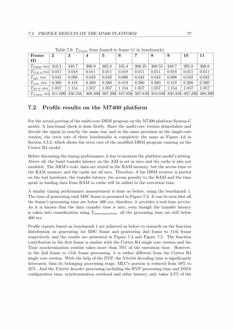
7.2. PROFILE RESULTS ON THE M7400 PLATFORM 77
Table 7.9: Tframe from frame2 to frame 11 in benchmark1
FrameID
2 3 4 5 6 7 8 9 10 11
TDRM ms 310.2 348.7 306.9 305.8 345.4 306.35 308.55 348.7 305.8 306.9
TDMA ms 0.011 0.018 0.011 0.011 0.018 0.011 0.011 0.018 0.011 0.011
Tsyn ms 0.042 0.066 0.042 0.042 0.066 0.042 0.042 0.066 0.042 0.042
Tcom ms 0.380 0.418 0.380 0.380 0.418 0.380 0.380 0.418 0.380 0.380
TEV P ms 1.057 1.154 1.057 1.057 1.154 1.057 1.057 1.154 1.057 1.057
Tframe ms 311.690 350.356 308.390 307.290 347.056 307.840 310.040 350.356 307.290 308.390
7.2 Profile results on the M7400 platform
For the actual porting of the multi-core DRM program on the M7400 platform System-Cmodel, A functional check is done firstly. Since the multi-core version demodulate anddecode the signal in exactly the same way and in the same precision as the single-coreversion, the error rate of three benchmarks is completely the same as Figure 4.6 inSection 4.3.2, which shows the error rate of the modified DRM program running on theCortex R4 model.
Before discussing the timing performance, it has to mention the platform model’s setting.Above all, the burst transfer latency on the AXI is set as zero and the cache is also notmodeled. The ARM’s code, data are stored in the RAM memory, but the access time tothe RAM memory and the cache are all zero. Therefore, if the DRM receiver is portedon the real hardware, the transfer latency, the access penalty to the RAM and the timespent in loading data from RAM to cache will be added to the execution time.
A similar timing performance measurement is done as before, using the benchmark 1.The time of generating each MSC frame is presented in Figure 7.3. It can be seen that allthe frame’s processing time are below 400 ms, therefore, it provides a real-time service.As it is known that the data transfer time is zero, even though the transfer latencyis taken into consideration using Tcommunication, all the processing time are still below400 ms.
Profile reports based on benchmark 1 are achieved as before to research on the functiondistribution on generating 1st MSC frame and generating 2nd frame to 11th framerespectively and the results are presented in Figure 7.4 and Figure 7.5. The functioncontribution in the first frame is similar with the Cortex R4 single core version and theTime synchronization routine takes more than 70% of the execution time. However,in the 2nd frame to 11th frame processing, it is rather different from the Cortex R4single core version. With the help of the EVP, the Viterbi decoding time is significantlydecreased, thus its belonging processing stage, MLC’s portion is reduced from 58% to25%. And the Viterbi decoder processing including the EVP processing time and DMAconfiguration time, synchronization overhead and other latency, only takes 3.5% of the
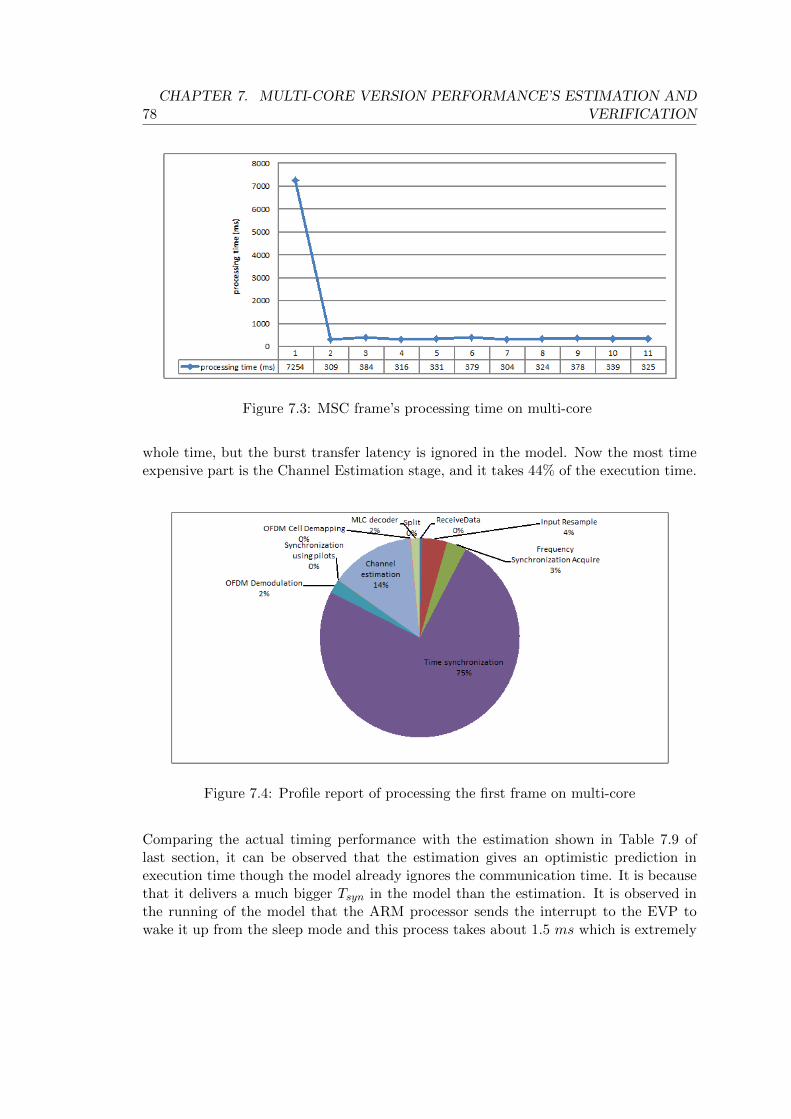
78CHAPTER 7. MULTI-CORE VERSION PERFORMANCE’S ESTIMATION AND
VERIFICATION
Figure 7.3: MSC frame’s processing time on multi-core
whole time, but the burst transfer latency is ignored in the model. Now the most timeexpensive part is the Channel Estimation stage, and it takes 44% of the execution time.
Figure 7.4: Profile report of processing the first frame on multi-core
Comparing the actual timing performance with the estimation shown in Table 7.9 oflast section, it can be observed that the estimation gives an optimistic prediction inexecution time though the model already ignores the communication time. It is becausethat it delivers a much bigger Tsyn in the model than the estimation. It is observed inthe running of the model that the ARM processor sends the interrupt to the EVP towake it up from the sleep mode and this process takes about 1.5 ms which is extremely

7.2. PROFILE RESULTS ON THE M7400 PLATFORM 79
Figure 7.5: Profile report of processing the 2nd to 11th frame on multi-core
high. And it happens in every EVP Viterbi processing and the time is various. Thusin a frame, for instance in Frame4, about 1.5 × 7 = 10.5 ms synchronization spent inwake-up, will occur. Normally, the EVP’s response to an interrupt will not takes such along time. It is the System-C model’s simulation process that leads to this.
We run the System-C model in the speed optimized mode. In the speed optimized mode,the two core models’ execution timing synchronization results in this high response andthis synchronization problem is called quantum effect. The ARM core and the EVP coreare modeled separately and each core emulates its execution time respectively. Usingthe Synopsys Virtual Prototype Analyzer, the execution time in each core is observed.When the ARM core sends the interrupt, it is in the time of 1, 432, 948, 100 ps and theEVP core which is in the sleep mode, is in the time of 2, 999, 114, 365 ps. Then themodel starts the two core’s synchronization, the EVP core’s time is kept and it doesnot execute instructions until the ARM core’s time reaches 2, 999, 114, 365 ps. Thenthe EVP core wakes up and starts the Viterbi decoding processing. Thus an additional1.567 ms response overhead appears. This model synchronization problem only appearsin the model and the program does not need to undergo this additional overhead in thereal hardware.
However, in the full optimized mode of the System-C model, this model’s time synchro-nization problem does not appear. The two core’s execution time is always synchronized.This full simulation mode also results in an about 500 times slower simulation speed com-paring with the optimized mode. In one second simulation time (the real word time onwatch), the speed optimized mode simulates 41 ms time of one EVP and one ARMcore’s running. However, the full simulation mode just simulates 0.074 ms running.This mode is in a extremely slow simulation speed. So the full simulation mode is notsuitable for simulating big and complex programs like DRM, though it does not have

80CHAPTER 7. MULTI-CORE VERSION PERFORMANCE’S ESTIMATION AND
VERIFICATION
the synchronization problem.
Another reason for the inaccurate estimation, is the error in the estimation of TDRM .It is calculated by using the function distribution in the whole process from 2nd frameto 11th frame and applying the distribution in each frame. However, in each frame,the distribution is approximately but not exactly the same as it is shown in section 4.1.Therefore, the achieving TDRM is not accurate.
In conclusion, the multi-core version DRM receiver’s processing speed can guarantee areal-time service based on the timing performance on the model which approximatelyaccords with the performance estimation in the last section. Compare with the single-core version on the Cortex R4, the multi-core version has a speed up of 1.7X and eachframe’s processing time is 339 ms in average as it is shown in Table 7.10.
Table 7.10: The multi-core version DRM’s speed upFrameID
2 3 4 5 6 7 8 9 10 11 AVG
SingleCorems
564 634 558 556 628 557 561 634 556 558 581
MultiCorems
309 384 316 331 379 304 324 378 339 325 338.9
SpeedUp
1.8 1.7 1.8 1.7 1.7 1.8 1.7 1.7 1.6 1.7 1.7

Chapter 8
Conclusion
8.1 Conclusion
This project’s main purpose is to accomplish a multi-core version of the DRM receiverprogram on the Ericsson M7400 platform. There are ARM Cortex R4 processor andEVP processor connected with the AXI bus on the platform. In the analysis of themulti-core version, the tool, Pareon is used to help to determine the communicationdata size in various versions.
The source code of the DRM receiver implementation is from the Dream DRM project.The code and its related libraries are analyzed and isolated to obtain an independent,compatible and minimal program only containing the main DRM receiving process. Thecorresponding benchmarks are also created to test the DRM’s functional correctnessand execution time. Before directly porting on the ARM core of the target platform, anintermediate porting step is achieved to port the DRM program on a simulation Cortex-A8 RTSM with a fast simulation speed. Based on the profile report, the DRM program isoptimized to increase the execution speed. After that, the modified code is ported on theCortex R4 model of the Ericsson platform. From the timing performance on the CortexR4 model, it can be seen that the frame processing time in average is 581 ms whichis far away from the real-time requirement. In order to further improve the processingspeed, the Viterbi decoder taking 45% of the execution time, is a candidate to port onEVP. An investigation is done to check if the Viterbi related code also should be portedto the EVP. The tool, Pareon is used here to analysis the data needed to be transferredin various multi-core versions. Through the analysis, it is chosen that only the Viterbidecoder function is chosen to port on EVP considering the improvement of the timeperformance , communication data size, EVP-C realization efficiency. Then the Viterbidecoding process on EVP as well as the communication controlled by DMA betweenthe ARM core and the EVP, are realized. Based on the multi-core distribution andcommunication design, the timing performance of the multi-core version DRM receiver
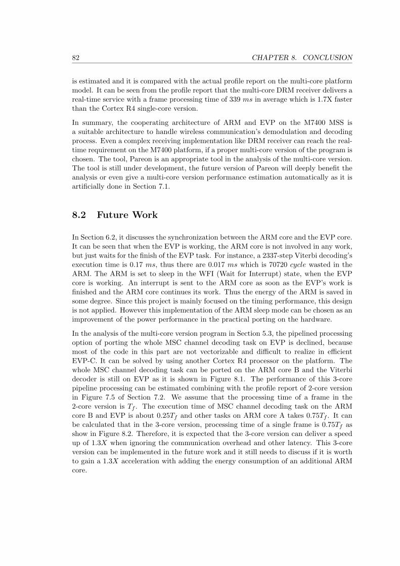
82 CHAPTER 8. CONCLUSION
is estimated and it is compared with the actual profile report on the multi-core platformmodel. It can be seen from the profile report that the multi-core DRM receiver delivers areal-time service with a frame processing time of 339 ms in average which is 1.7X fasterthan the Cortex R4 single-core version.
In summary, the cooperating architecture of ARM and EVP on the M7400 MSS isa suitable architecture to handle wireless communication’s demodulation and decodingprocess. Even a complex receiving implementation like DRM receiver can reach the real-time requirement on the M7400 platform, if a proper multi-core version of the program ischosen. The tool, Pareon is an appropriate tool in the analysis of the multi-core version.The tool is still under development, the future version of Pareon will deeply benefit theanalysis or even give a multi-core version performance estimation automatically as it isartificially done in Section 7.1.
8.2 Future Work
In Section 6.2, it discusses the synchronization between the ARM core and the EVP core.It can be seen that when the EVP is working, the ARM core is not involved in any work,but just waits for the finish of the EVP task. For instance, a 2337-step Viterbi decoding’sexecution time is 0.17 ms, thus there are 0.017 ms which is 70720 cycle wasted in theARM. The ARM is set to sleep in the WFI (Wait for Interrupt) state, when the EVPcore is working. An interrupt is sent to the ARM core as soon as the EVP’s work isfinished and the ARM core continues its work. Thus the energy of the ARM is saved insome degree. Since this project is mainly focused on the timing performance, this designis not applied. However this implementation of the ARM sleep mode can be chosen as animprovement of the power performance in the practical porting on the hardware.
In the analysis of the multi-core version program in Section 5.3, the pipelined processingoption of porting the whole MSC channel decoding task on EVP is declined, becausemost of the code in this part are not vectorizable and difficult to realize in efficientEVP-C. It can be solved by using another Cortex R4 processor on the platform. Thewhole MSC channel decoding task can be ported on the ARM core B and the Viterbidecoder is still on EVP as it is shown in Figure 8.1. The performance of this 3-corepipeline processing can be estimated combining with the profile report of 2-core versionin Figure 7.5 of Section 7.2. We assume that the processing time of a frame in the2-core version is Tf . The execution time of MSC channel decoding task on the ARMcore B and EVP is about 0.25Tf and other tasks on ARM core A takes 0.75Tf . It canbe calculated that in the 3-core version, processing time of a single frame is 0.75Tf asshow in Figure 8.2. Therefore, it is expected that the 3-core version can deliver a speedup of 1.3X when ignoring the communication overhead and other latency. This 3-coreversion can be implemented in the future work and it still needs to discuss if it is worthto gain a 1.3X acceleration with adding the energy consumption of an additional ARMcore.

8.2. FUTURE WORK 83
Figure 8.1: The pipelined 3-core version
In this project, we focuse on the main DRM processing including demodulation, de-mapping and channel decoding. However, the complete DRM receiver should also includethe source decoding stage. It can be implemented in a Codec (coder-decoder) processoroutside the platform to perform the audio decoding task. What’s more, it can be seenthat the processing of the first frame takes a large amount of time, for instance, it isabout 7 s in the benchmark 1. The antenna continuously receives the radio signal, butthe received data cannot be processed immediately. Thus based on the latency of thefirst frame, a corresponding size of the memory is needed to store the received signalswhich cannot be handled in time.

84 CHAPTER 8. CONCLUSION
Figure 8.2: The pipelined frame processing in 3-core version

Appendix A.
ARM Linker configuration onCortex R4
This part discusses the ARM linker configuration on Cortex R4 model. The ARM linkercombines the contents of one or more object files with selected parts of one or more objectlibraries to produce an ARM ELF image [34]. For the library, the link can automaticallyselect the appropriate standard C or C++ library variants to link with, based on thebuild attributes of the objects it is linking [34]. Therefore, it is not necessary to indicatewhich library has to be linked.
The ELF image structure is divided into 3 parts, namely RO section, RW section and ZIsection. The RO section contains code and Read-Only (RO) data. The RO data includesthe addresses of variables that are accessed by the code, floating-point immediate values,immediate values that cannot be loaded directly into a register and so on. Read-Write(RW) data stores in RW section and the Read-Write data which is zero-initialized atimage startup is called Zero-Initialized (ZI) data is in the ZI section. [35]
The image is firstly load into memory before execution. In the load view, the RWsection and RO section are loaded into the ROM. When starting execution, the ZIsection is created and loaded into RAM together with RW section. The load view andthe execution view are presented in Figure A..1. The loading address of each section canbe defined.
Except the RW section and ZI section, there are stack and heap in RAM. Stack is used tohandle processor exceptions. There are 7 kinds of exceptions including Reset, UndefinedInstruction, Software Interrupt (SWI), Pre-fetch Abort, Data Abort, IRQ as well as FIQ[35]. The stack is used to store the contents of any registers if an exception occurs andre-store them when returning. Heap defines dynamically-allocated read-write memory.It is used to create new variables, for instance, when the C/C++ language functionmalloc() is called, it will create a space in the heap memory. The address and size ofheap and stack also can be configured.
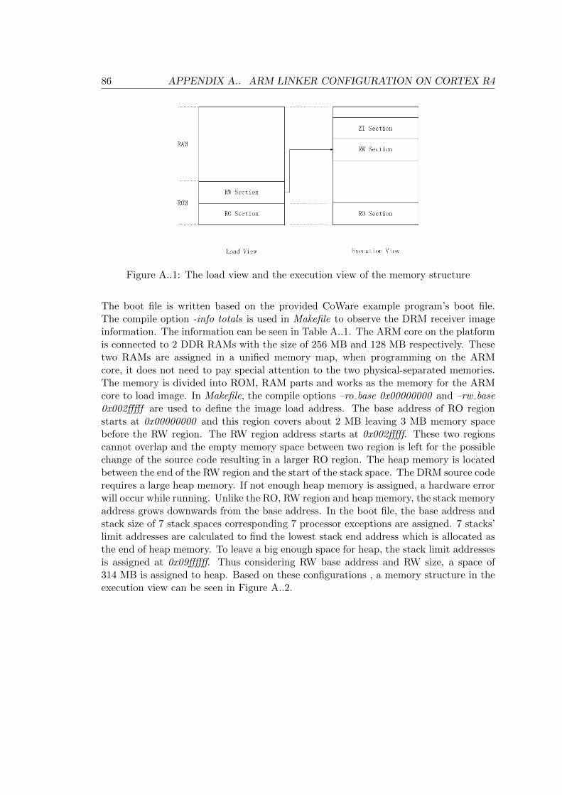
86 APPENDIX A.. ARM LINKER CONFIGURATION ON CORTEX R4
Figure A..1: The load view and the execution view of the memory structure
The boot file is written based on the provided CoWare example program’s boot file.The compile option -info totals is used in Makefile to observe the DRM receiver imageinformation. The information can be seen in Table A..1. The ARM core on the platformis connected to 2 DDR RAMs with the size of 256 MB and 128 MB respectively. Thesetwo RAMs are assigned in a unified memory map, when programming on the ARMcore, it does not need to pay special attention to the two physical-separated memories.The memory is divided into ROM, RAM parts and works as the memory for the ARMcore to load image. In Makefile, the compile options –ro base 0x00000000 and –rw base0x002fffff are used to define the image load address. The base address of RO regionstarts at 0x00000000 and this region covers about 2 MB leaving 3 MB memory spacebefore the RW region. The RW region address starts at 0x002fffff. These two regionscannot overlap and the empty memory space between two region is left for the possiblechange of the source code resulting in a larger RO region. The heap memory is locatedbetween the end of the RW region and the start of the stack space. The DRM source coderequires a large heap memory. If not enough heap memory is assigned, a hardware errorwill occur while running. Unlike the RO, RW region and heap memory, the stack memoryaddress grows downwards from the base address. In the boot file, the base address andstack size of 7 stack spaces corresponding 7 processor exceptions are assigned. 7 stacks’limit addresses are calculated to find the lowest stack end address which is allocated asthe end of heap memory. To leave a big enough space for heap, the stack limit addressesis assigned at 0x09ffffff. Thus considering RW base address and RW size, a space of314 MB is assigned to heap. Based on these configurations , a memory structure in theexecution view can be seen in Figure A..2.

87
Table A..1: The DRM receiver ELF image informationRO Size RW Size ROM Size
Equation Code+RO Data RW Data+ZI Data Code+RO Data+RW Data
Value (Kb) 630.65 1768.89 2385.68
Figure A..2: The execution view of the configured memory structure

88 APPENDIX A.. ARM LINKER CONFIGURATION ON CORTEX R4

Appendix B.
Multicore Communications API’simplementation
In order to modularize the multi-core communication achieved between the EVP andARM processors, and help the further analysis of the Pareon software, the MulticoreCommunications API (MCAPI) is applied to design the communication interfaces in theDRM two-core version.
The MCAPI defines an API and a semantic for communication and synchronizationbetween cores in embedded system [36]. However, it is a high level application anddoes not involve the lower level definition including protocol, hardware model and otherdetailed settings.
MCAPI consists of these major concepts. An MCAPI domain could be a single chipwith multiple cores or multiple processor chips on a board and it stands for one or moreMCAPI nodes in a multicore topology. The MCAPI node is an independent threadof control, such as a process, thread, processor, hardware accelerator, or instance ofan operating system [36]. MCAPI endpoints are socket-like communication-terminationpoints. A node can have multiple endpoints. Thus, an endpoint contains a topology-global unique identifier < domain id, node id, port id >.
MCAPI [36] delivers three fundamental communications types, namely Message, PacketChannel as well as Scalar Channel. The latter two types are chosen in our design.Packet Channel transmits connection-oriented, unidirectional, FIFO packet streams andconnection-oriented, single-word, unidirectional, FIFO scalar streams are sent by ScalarChannel [36]. Channels are set up at initialization. Once built, the channel can achievethe data transfer with little overhead. When the data reaches the destination endpoint,it is added to an endpoint receive queue. The data typically remains in the endpoint’sreceive queue until it is received by the application that owns the endpoint.
The design is based on the two-core architecture platform. The platform is defined as

90 APPENDIX B.. MULTICORE COMMUNICATIONS API’S IMPLEMENTATION
domain 0. The core for the DRM main processing is assigned as node 0 and anotherfor the Viterbi decoder is node 1. Each node contains 4 endpoints to set 4 channelsfor communication. 2 Packet Channels are implemented to perform the Viterbi inputdata transfer and Viterbi output data transfer respectively. Scalar Channels are usedto acknowledge the finish of the Viterbi decoding and realize the synchronization of thecommunication. The detailed design is presented in Figure B..1.
The Multicore communication API Working Group provides some head files containingcommunication functions to help detailed design. The head files used here are mca.h,mcapi.h, mca impl spec.h as well as mcapi impl spec.h.
The first step is to initialize nodes and bind the channel in Figure B..2. Once set up, twonodes can communicate with the binding channel. mcapi node init attributes is used toinitialize the data type defining the node attribute. Then mcapi initialize is implementedto apply the node attribute to initialize the node. Thus the initialization of the node hasbeen done. The function mcapi endpoint create is applied to create an endpoint. Theendpoint is created dynamically which means a global variable MCAPI PORT ANYis involved to indicate the next available endpoint on the local node. The endpointis statically created using the static ID in the remote node and obtained in the localnode by mcapi endpoint get. mcapi endpoint get is a blocking function. It blocks untilthe specified remote endpoint has been created or a timeout is reached. After that,mcapi pktchan connect i is located to bind the a Packet Channel and the behavior ofopen a local send port is achieved by mcapi pktchan send open i. While the open func-tion mcapi pktchan recv open i is used in the remote node to synchronize and initializethe local packet receive port. Thus a Packet Channel is bound. The Scalar Channel iscreated in the same way.

91
Figure B..1: MCAPI design

92 APPENDIX B.. MULTICORE COMMUNICATIONS API’S IMPLEMENTATION
Figure B..2: MCAPI implementation in node initialization and binding channel

93
The communication is designed on the established channel in Figure B..3. The Viterbidecoding input data waited to send is wrapped into packets and stored in the endpointbuffer. The function get next packet is applied to judge whether the next package isavailable. If so, the package is delivered to the remote end point by mcapi pktchan sendthrough the Packet Channel. Otherwise, it sends a scalar signal through the ScalarChannel, to the remote end to inform the end of transfer. While in the remote end,mcapi pktchan recv receives the package from the channel. After finishing one timereceiving, a judgment should be done by mcapi sclchan available to detect the inform-ing signal. Once it detects that the transferring has ended, the remote end invokesmcapi pktchan release to return the packet buffers to the system, thus the received datais available to use and the Viterbi decoding routine can be called. Afterwards, the de-coded data is packaged and sent back the acknowledge signal to the local end to tellthat the work has been finished. Then a similar transfer as before is launched to sendthe output data back to the local end by package.
Once the MCAPI design is finished, these API communication functions can be instanti-ated combing the real hardware. For instance, if it is implemented in the Ericsson M7400platform, the packet sending function mcapi pktchan send is written to launch a DMAtransfer. After the MCAPI design and instantiation, these API communications canbe called in the program to realize the communication design. And the modularizationcommunication is also easy to apply in the various multi-core versions.
For example, if the pipelined multi-core version mentioned in section 5.3 is expectedto implemented, the whole MSC channel decoding processing stage is ported on EVPand the communication between the ARM and EVP needs to redesign using the APIfunctions as it is presented in Figure B..4. It is different from the former design becauseit does not need synchronization. When the ARM’s task is finished, it packs the dataand stores the packets in the buffer of the endpoint. Then the non-blocking functionmcapi pktchan send i is called. This function returns immediately and the node doesnot have to wait the transmit to finish. Once the transfer request is sent, the ARMcan continue to do the processing of the next frame. When the packet reaches thedestination endpoint, it is added to an endpoint receive queue. In the EVP end, oncethe EVP finishes the current task, it uses mcapi pktchan recv to receive the packet fromthe queue and store in the buffer. When enough data is gained for one time routine, itcalls the function mcapi pktchan release to obtain the data from the buffer and processthe routine.

94 APPENDIX B.. MULTICORE COMMUNICATIONS API’S IMPLEMENTATION
Figure B..3: MCAPI implementation in communication
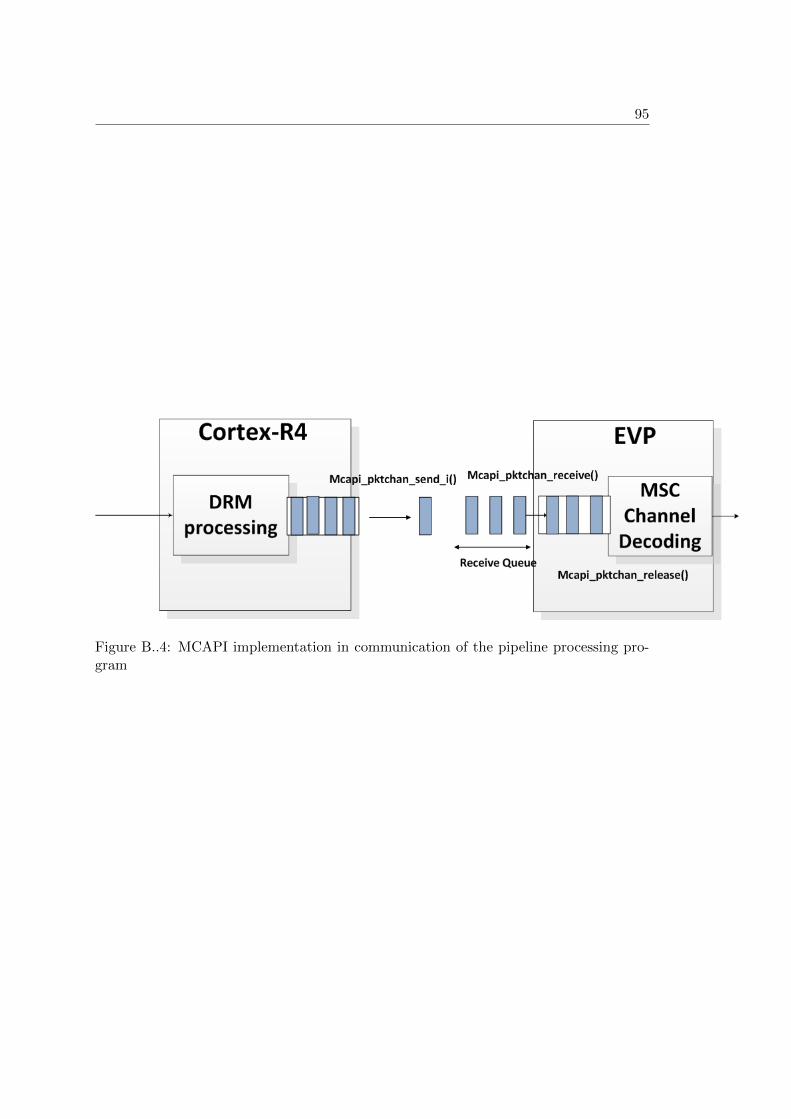
95
Figure B..4: MCAPI implementation in communication of the pipeline processing pro-gram

96 APPENDIX B.. MULTICORE COMMUNICATIONS API’S IMPLEMENTATION
Bibliography
[1] Hyunseok Lee, Yuan Lin, Yoav Harel, Mark Woh, Scott Mahlke, Trevor Mudge, andKrisztian Flautner. Software defined radio–a high performance embedded challenge.High Performance Embedded Architectures and Compilers, pages 6–26, 2005.
[2] Markus Dillinger, Kambiz Madani, and Nancy Alonistioti. Software defined radio:Architectures, systems and functions. Wiley. com, 2005.
[3] Mathew NO Sadiku and Cajetan M Akujuobi. Software-defined radio: a briefoverview. Potentials, IEEE, 23(4):14–15, 2004.
[4] Friedrich K Jondral. Software-defined radio: basics and evolution to cognitive radio.EURASIP Journal on Wireless Communications and Networking, 2005(3):275–283,2005.
[5] Joe Mitola. The software radio architecture. Communications Magazine, IEEE,33(5):26–38, 1995.
[6] Drm introduction and implementation guide. http://www.drm.org/.
[7] TS ETSI. 101980.digital radio mondiale (drm): System specification, 2001.http://www.etsi.org/.
[8] AndrTavares Coutinho. Drm analysis using a simulator of multiprocessor embeddedsystem, 2008. http://ria.ua.pt/bitstream/10773/1950/1/2009000406.pdf.
[9] Lodewijk T Smit, Johann L Hurink, and Gerard JM Smit. Run-time mapping ofapplications to a heterogeneous soc. In System-on-Chip, 2005. Proceedings. 2005International Symposium on, pages 78–81. IEEE, 2005.
[10] Vector fabrics offical website http://www.vectorfabrics.com/.
[11] AF Kurpiers and Volker Fischer. Open-source implementation of a digital radiomondiale (drm) receiver. In HF Radio Systems and Techniques, 2003. Ninth Inter-national Conference on (Conf. Publ. No. 493), pages 86–90. IET, 2003.
[12] Fftw offical website http://www.fftw.org/.
[13] Digital radio mondiale (drm): Mw simulcast tests in mexico, http://www.drm.org/.

98 BIBLIOGRAPHY
[14] Arm offical website http://www.arm.com/.
[15] Katie Roberts-Hoffman and Pawankumar Hegde. Arm cortex-a8 vs. intel atom:Architectural and benchmark comparisons. Dallas: University of Texas at Dallas,2009.
[16] Emily Blem, Jaikrishnan Menon, and Karthikeyan Sankaralingam. A detailed anal-ysis of contemporary arm and x86 architectures. Technical report, Technical report,UW-Madison, 2013.
[17] Danilo Beuche, Abdelaziz Guerrouat, Holger Papajewski, Wolfgang Schroder-Preikschat, Olaf Spinczyk, and Ute Spinczyk. The pure family of object-orientedoperating systems for deeply embedded systems. In Object-Oriented Real-Time Dis-tributed Computing, 1999.(ISORC’99) Proceedings. 2nd IEEE International Sym-posium on, pages 45–53. IEEE, 1999.
[18] Arm architecture reference manual armv7-a and armv7-r edition errata markup.http://infocenter.arm.com/.
[19] Cortex-r4 white paper http://infocenter.arm.com/.
[20] Cortex-r4 and cortex-r4f revision: r1p3 technical reference manualhttp://infocenter.arm.com/.
[21] Kees van Berkel, Anteneh Abbo, Srinivasan Balakrishnan, Richard Kleihorst,Patrick PE Meuwissen, and Rick Nas. Vector processing as an enabler for ambi-ent intelligence. In AmIware Hardware Technology Drivers of Ambient Intelligence,pages 223–243. Springer, 2006.
[22] Akash Kumar and Kees van Berkel. Vectorization of reed solomon decoding andmapping on the evp. In Proceedings of the conference on Design, automation andtest in Europe, pages 450–455. ACM, 2008.
[23] Yuan Lin, Hyunseok Lee, Mark Woh, Yoav Harel, Scott Mahlke, Trevor Mudge,Chaitali Chakrabarti, and Krisztian Flautner. Soda: A low-power architecture forsoftware radio. In ACM SIGARCH Computer Architecture News, volume 34, pages89–101. IEEE Computer Society, 2006.
[24] Sudeep Pasricha and Nikil Dutt. On-chip communication architectures: system onchip interconnect. Morgan Kaufmann, 2010.
[25] Arm ds-5 version 5.13 eb rtsm reference guide. http://infocenter.arm.com/.
[26] Gcc online documentation. http://gcc.gnu.org/.
[27] Dhrystone benchmark http://www.roylongbottom.org.uk/.
[28] Whetstone benchmark http://netlib.org/benchmark/whetstone.c.
[29] Cortex-a8 revision: r1p1 technical reference manual http://infocenter.arm.com/.
BIBLIOGRAPHY 99
[30] Assessing cortex-r4 and cortex-a8 signal and media processing performancehttp://www.bdti.com/.
[31] Realview compilation tools version 2.2 compiler and libraries guidehttp://infocenter.arm.com/.
[32] Kelvin Yi-Tse Lai. An efficient metric normalization architecture for high-speedlow-power viterbi decoder. In TENCON 2007-2007 IEEE Region 10 Conference,pages 1–4. IEEE, 2007.
[33] John Davis, Andrew Lin, and Ayodele Thomas Njuguna Njoroge. Viterbi algorithmsas a stream application. ”signal”, 1:2, 2002.
[34] Realview compilation tools linker user guide http://infocenter.arm.com/.
[35] Arm developer suite version 1.2 developer guide http://infocenter.arm.com/.
[36] Mcapi api specification v2.015. http://www.multicore-association.org/.