post-silicon debug of complex multi clock and power domain...
TRANSCRIPT
Post-Silicon Debug of Complex Multi Clock and Power Domain ICs
Bradley R. Quinton, Andrew M. Hughes
Veridae Systems, Inc. Vancouver, Canada
{bradq,andrewh}@veridae.com
Steven J.E. Wilton University of British Columbia
Vancouver, Canada [email protected]
Abstract Post-silicon debug is becoming a major issue for Integrated Circuit (IC) designers. Proposals are emerging to help reduce the debug time of ICs. Modern ICs, however, are extremely large and complex, and they present a number of critical challenges to an effective debug solution. Multi clock and power domain issues, in particular, present significant challenges to existing solutions. In this paper we describe how our debug infrastructure uses a system-level design approach to address these difficult issues. By using our debug insertion tool and special-purpose hardware IP, IC designers can create debug solutions that are tuned to their specific designs and debug requirements. Debug functionality is integrated using a hierarchical, scalable, plug-and-play approach. The infrastructure is flexible enough to cleanly support chips with multiple clock and power domains, and complex design hierarchies while minimizing area, clocking and routing impacts. 1. Introduction
The growing time and effort required for post-silicon debug and validation has become a major concern in the semiconductor industry [1,2,3,4]. Moore’s Law scaling drives this problem. As each new process node reduces transistor cost, and, therefore, drives further functional integration [5], the post-silicon validation problem grows on three fronts: 1) the increase in overall functionality increases the total number of features that must operate correctly; 2) the increase in integration necessitates heterogeneous, complex, error-prone, feature interaction; and 3) limited external I/O significantly reduces the external visibility into the operation of the system. These challenges have led to a number of proposals to assist of the debug of post-silicon systems [6,7,8,9,10,11]. Although these proposals handle specific aspects of the debug process, critical challenges remain. In this paper we focus on the integration of our debug infrastructure into complex multi clock and power domain ICs. We describe the challenges and explain how our infrastructure addresses these challenges.
Most new ICs have at least two or three different clock
domains, and some have as many as 100 different clock
domains [12,13]. In addition, to reduce power consumption, many ICs adopt complex power saving techniques such as fine- and coarse-grained clock gating, power gating and dynamic clock and voltage scaling [14]. To be effective a post-silicon debug infrastructure must not only integrate simply and effectively into these ICs, but they must also be able to assist in the complex task of debugging issues that arises because of these new features.
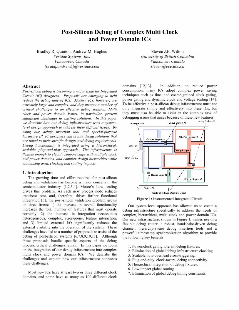
Figure 1: Instrumented Integrated Circuit
Our system-level approach has allowed us to create a debug infrastructure specifically to address the needs of complex, hierarchical, multi clock and power domain ICs. Our new infrastructure, shown in Figure 1, makes use of a flexible debug router, a robust, handshake-driven debug channel, hierarchy-aware debug insertion tools and a powerful timestamp synchronization algorithm to provide the following key benefits:
1. Power/clock gating tolerant debug fixtures. 2. Elimination of global debug infrastructure clocking. 3. Scalable, low-overhead cross-triggering. 4. Plug-and-play, clock-aware, debug connectivity. 5. Hierarchical integration of debug fixtures. 6. Low impact global routing. 7. Elimination of global debug timing constraints.

The remainder of this paper is organized as follows. In Section 2, we elaborate on the challenges of creating an effective post-silicon debug solution. Then, in Section 3, we present an overview of the operation and usage model for our debug infrastructure. In Section 4, we describe the details debug channel, and in Section 5 we summarize the details of two of our debug fixtures. Finally we conclude with a summary in Section 6. 2. Challenges
Creating an effective post-silicon debug solution for complex multi clock and power domain ICs presents a number of challenges, these are explained in detail in the subsections below. 2.1 Hierarchical Design and Third-party IP
The design of complex ICs requires the efforts of large engineering teams. To manage this complexity ICs are normally implemented hierarchically. Design blocks are connected to form subsystems and subsystems are connected to create large, complex ICs. These blocks and subsystems are created by different engineers, often in different locations, and in the case of third-party IP, even in different companies. To be effective, a debug solution must fit this paradigm. Engineers working on different aspects of an IC often have limited understanding of the details of other blocks in a design. These designers must, therefore, be able to deliver their blocks with design-specific debug capabilities built-in, and these debug capabilities must be able to inter-operate, seamlessly, with debug capabilities in others parts of the chip. Furthermore, designers must be able to “close-off” their designs, such that they don’t need to be modified as they are used (and often, re-used) in different subsystems and ICs. 2.2 Clock Domains and Global Synchronization
The size, complexity and heterogeneous nature of the systems implemented in modern ICs has driven the need support multiple clocks domains on a single IC. Often, design blocks must operate at a prescribed “line-rate” to meet the requirements of an industry-standard interface. In addition, the power and performance requirements of different designs often demand different clock rates. Debug solutions must not only be aware of these issues since they are the cause of many bugs, but must fit naturally into these ICs without imposing onerous clocking and global synchronization requirements on the system as a whole. 2.3 Clock and Power Gating
In order to maintain power dissipation budgets while increasing transistor counts, mainstream ICs are now making wide use of the advanced power-management techniques such as clock and power gating. In general, these techniques allow the systems to “turn-off” parts of the IC that are not being used, thereby limiting the power
dissipation. Either software or hardware may statically or dynamically control this gating. Like multiple clock domains, these features are often the source of complex bugs. An effective debug solution must be tolerant to the effects of clock and power gating, and ideally will provide an effective means to debug issues relating to clock and power gating. 2.4 Scalable Cross-triggering and Synchronization
Many of the most complex and hard-to-find bugs in ICs are the result of interactions between different blocks and subsystems, which are often in different clock domains. To be effective a debug solution must support the synchronization of debug events within these different clock domains; this is called cross-triggering. As systems grow large it is critical that a debug system scales such that the resources and design effort required for cross-triggering do not become unsupportable. 2.5 Global Routing
Global routing can be a challenge in modern IC design for a number of reasons. The effects of process scaling have increased the proportion of overall circuit delay attributable to wire delay, making the timing of global routing more unpredictable. In addition, signal integrity issues and on-die process variation make the process of managing the timing of large numbers of global wires problematic. For these reasons it is important that a debug infrastructure has a minimum impact on global routing of an IC. To do this the infrastructure must minimize the total number of wires routed at the top-level of the device and not impose difficult timing constraints.
Figure 2: Debug Fixtures
3. Overview 3.1 Basic Theory of Operation
To address the challenges outlined in Section 2 we have created a debug infrastructure that uses a special-purpose network to enable communication between any number of independent debug stations, as shown in Figure 1. The communication between stations is done using a narrow (8-bit) handshake-driven debug channel. Each station connects to one or more debug fixtures, using an industry standard AMBA APB interface as shown in Figure 2. These
debug fixtures implements debug tasks such as data capture, event generation, signal selection and hardware assertions. Each of the station and fixture combinations may each operate at a different clock frequency without the need for a global clock. The topology of the network can be easily crafted to meet the specific clocking, power-gating and global routing requirements of each target IC. Each station implements an extendable, memory-mapped address space that is accessible (through a JTAG probe) to our off-chip software, or to IC-specific on-chip software. The network uses an intelligent router and auto-enumeration to ensure correct operation through clock and power gating events. In addition the network supports in-band, asynchronous event generation and to enable scalable, robust cross-triggering. 3.2 Overall Usage Model 3.2.1 Design phase
The debug infrastructure itself is both planned, and automatically incorporated into the design, using our software tools. The software tools operate hierarchically and can be run by different users at the block, subsystem and chip-level. The outputs from one level of hierarchy are passed “up” to the next level.
Our Debug Planner Tool helps designers to plan the
number of debug stations, the network topology, the number of debug fixtures and the configuration of these debug fixtures by providing detailed area overhead analysis along with estimates to the relative debug effectiveness of these choices. In addition, given a Verilog or VHDL design, our tool helps determines which signals are likely to be of high value during debug. The user can then use this
information to guide the selection of the specific instantiation of architecture for their specific chip.
Our Debug Instrumentor Tool uses the debug plan
generated by the Debug Planner to automatically modify the user’s design (at the RTL level) by adding the appropriate debug circuitry to implement the debug infrastructure. At the same time the Debug Instrumentor automatically generates test benches, timing verification scripts, and formal analysis scripts to ensure that the changes have been made correctly. 3.2.2 Debug phase
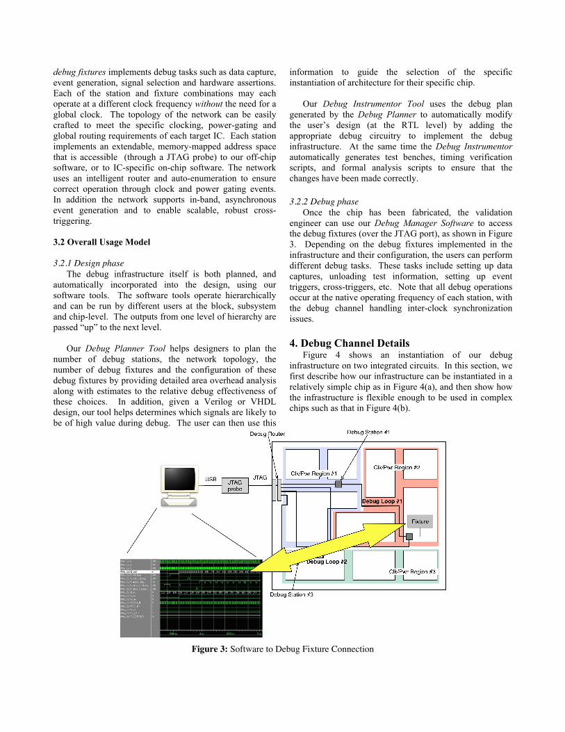
Once the chip has been fabricated, the validation engineer can use our Debug Manager Software to access the debug fixtures (over the JTAG port), as shown in Figure 3. Depending on the debug fixtures implemented in the infrastructure and their configuration, the users can perform different debug tasks. These tasks include setting up data captures, unloading test information, setting up event triggers, cross-triggers, etc. Note that all debug operations occur at the native operating frequency of each station, with the debug channel handling inter-clock synchronization issues. 4. Debug Channel Details
Figure 4 shows an instantiation of our debug infrastructure on two integrated circuits. In this section, we first describe how our infrastructure can be instantiated in a relatively simple chip as in Figure 4(a), and then show how the infrastructure is flexible enough to be used in complex chips such as that in Figure 4(b).
Figure 3: Software to Debug Fixture Connection
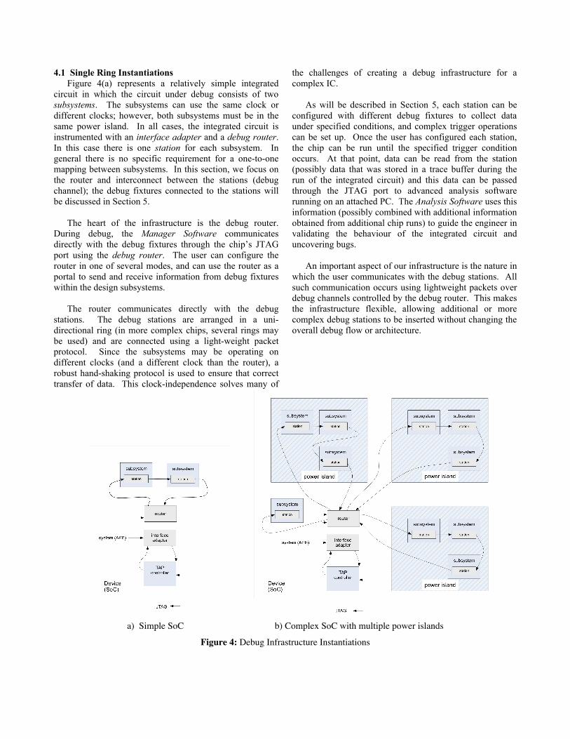
4.1 Single Ring Instantiations Figure 4(a) represents a relatively simple integrated
circuit in which the circuit under debug consists of two subsystems. The subsystems can use the same clock or different clocks; however, both subsystems must be in the same power island. In all cases, the integrated circuit is instrumented with an interface adapter and a debug router. In this case there is one station for each subsystem. In general there is no specific requirement for a one-to-one mapping between subsystems. In this section, we focus on the router and interconnect between the stations (debug channel); the debug fixtures connected to the stations will be discussed in Section 5.
The heart of the infrastructure is the debug router.
During debug, the Manager Software communicates directly with the debug fixtures through the chip’s JTAG port using the debug router. The user can configure the router in one of several modes, and can use the router as a portal to send and receive information from debug fixtures within the design subsystems.
The router communicates directly with the debug
stations. The debug stations are arranged in a uni-directional ring (in more complex chips, several rings may be used) and are connected using a light-weight packet protocol. Since the subsystems may be operating on different clocks (and a different clock than the router), a robust hand-shaking protocol is used to ensure that correct transfer of data. This clock-independence solves many of
the challenges of creating a debug infrastructure for a complex IC.
As will be described in Section 5, each station can be
configured with different debug fixtures to collect data under specified conditions, and complex trigger operations can be set up. Once the user has configured each station, the chip can be run until the specified trigger condition occurs. At that point, data can be read from the station (possibly data that was stored in a trace buffer during the run of the integrated circuit) and this data can be passed through the JTAG port to advanced analysis software running on an attached PC. The Analysis Software uses this information (possibly combined with additional information obtained from additional chip runs) to guide the engineer in validating the behaviour of the integrated circuit and uncovering bugs.
An important aspect of our infrastructure is the nature in
which the user communicates with the debug stations. All such communication occurs using lightweight packets over debug channels controlled by the debug router. This makes the infrastructure flexible, allowing additional or more complex debug stations to be inserted without changing the overall debug flow or architecture.
a) Simple SoC b) Complex SoC with multiple power islands
Figure 4: Debug Infrastructure Instantiations
4.2 Complex Instantiations Figure 2(b) shows a more complex integrated circuit
with multiple power islands. As before, each subsystem is instrumented with a single debug station. Rather than arranging the stations in a single ring, however, here we use multiple rings. This is critical; the use of multiple rings means that the debug circuitry will still operate if part of the chip is powered down during normal operation (as is common in chips targeting the low power domain). If one power island is powered down, the stations in the remaining islands can continue to collect data and monitor their trigger signals. The Manager Software and the debug router hardware automatically manage these events.
The partitioning of the debug infrastructure into
multiple debug stations is performed by the integrated circuit designer using the Debug Planner. Designers already know how the chip is partitioned into islands, and the major subsystem breakdown of their chip, so we allow the designer to use this information in creating a customized debug solution for their specific chip. 5. Debug Fixtures Details
Our infrastructure is flexible enough to support a variety of debug fixtures and the interface between the stations and the fixtures can easily be extended in the future. Although the details of the debug fixtures are not the focus of this paper, we will summarize the functionality of two fixtures (a trace buffer and a hierarchical debug access network) to help build an overall picture of the infrastructure. 5.1 Trace Buffer
The trace buffer based debug fixture gathers data from the subsystem under debug, and then stores this information in a local trace buffer. Our trace buffers employ a number of advanced techniques to maximize the amount of data that can be stored in given amount of memory. These techniques include lossless compression algorithms, arbitrary bit-packing of data, programmable, selective data capture capabilities, and advanced clock encoding methodologies. In addition, the fixture monitors selected trigger signals, and participates with other fixtures in the overall trigger detection using the cross-triggering techniques discussed earlier. 5.3 Hierarchical Debug Access Network
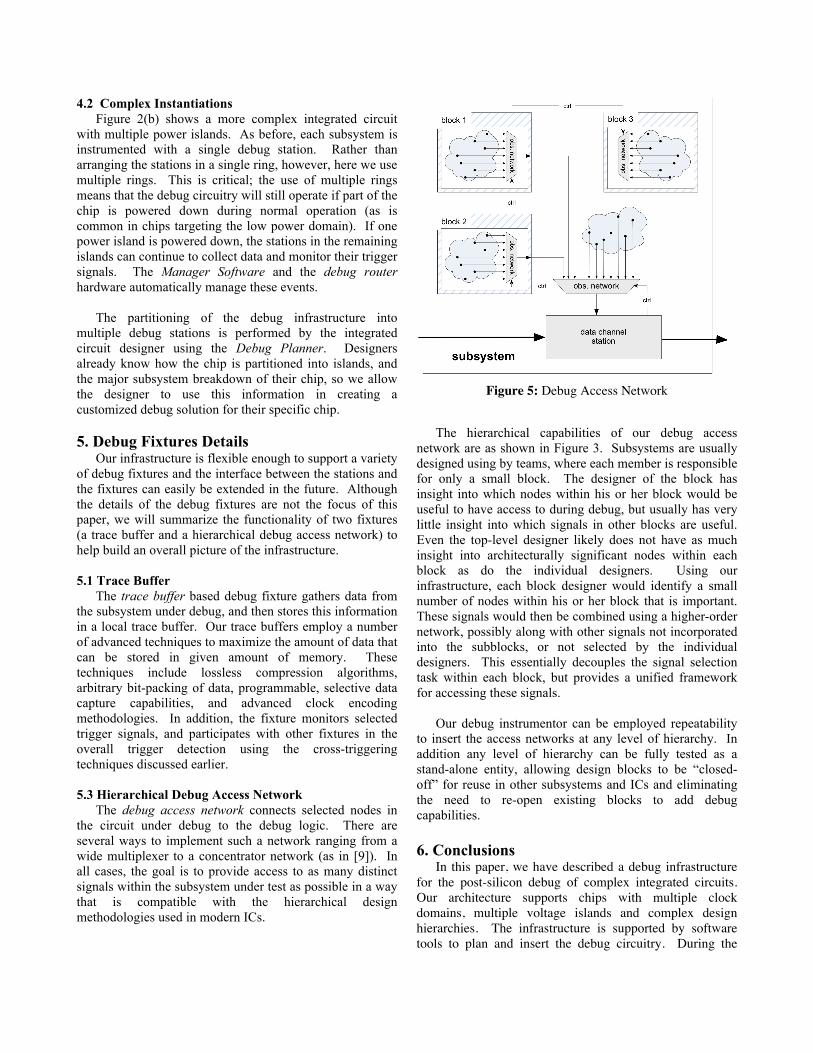
The debug access network connects selected nodes in the circuit under debug to the debug logic. There are several ways to implement such a network ranging from a wide multiplexer to a concentrator network (as in [9]). In all cases, the goal is to provide access to as many distinct signals within the subsystem under test as possible in a way that is compatible with the hierarchical design methodologies used in modern ICs.
Figure 5: Debug Access Network
The hierarchical capabilities of our debug access
network are as shown in Figure 3. Subsystems are usually designed using by teams, where each member is responsible for only a small block. The designer of the block has insight into which nodes within his or her block would be useful to have access to during debug, but usually has very little insight into which signals in other blocks are useful. Even the top-level designer likely does not have as much insight into architecturally significant nodes within each block as do the individual designers. Using our infrastructure, each block designer would identify a small number of nodes within his or her block that is important. These signals would then be combined using a higher-order network, possibly along with other signals not incorporated into the subblocks, or not selected by the individual designers. This essentially decouples the signal selection task within each block, but provides a unified framework for accessing these signals.
Our debug instrumentor can be employed repeatability
to insert the access networks at any level of hierarchy. In addition any level of hierarchy can be fully tested as a stand-alone entity, allowing design blocks to be “closed-off” for reuse in other subsystems and ICs and eliminating the need to re-open existing blocks to add debug capabilities. 6. Conclusions
In this paper, we have described a debug infrastructure for the post-silicon debug of complex integrated circuits. Our architecture supports chips with multiple clock domains, multiple voltage islands and complex design hierarchies. The infrastructure is supported by software tools to plan and insert the debug circuitry. During the
debug phase, software running on a external PC controls the infrastructure and executes off-chip analysis algorithms. References: [1] S. Sandler, “Need for debug doesn’t stop at first
silicon”, E.E. Times, February 21, 2005. [2] R. Goering, “Post-silicon debugging worth a second
look”, E.E. Times, May 2, 2007. [3] A.B.T. Hopkins, K.D. McDonald-Maier, “Debug
support for complex systems on-chip: a review”, IEE Proceedings - Computer and Digital Technology, vol. 153, no. 4, July 2006.
[4] P. Patra, “On the Cusp of a Validation Wall”, IEEE Design & Test of Computers, Vol. 24, No. 2, pp. 193-196, Mar./Apr. 2007.
[5] International Technology Roadmap for Semiconductors (ITRS), 2007 Report, http://www.itrs.net, 2008.
[6] M. Riley, M. Genden, “Cell Broadband Engine Debugging for Unknown Events”, IEEE Design and Test of Computers, vol. 24, no. 5, pp. 486-493, September/October 2007.
[7] T. J. Foster, et al., “First Silicon Functional Validation and Debug of Multicore Microprocessors”, IEEE Transactions on Very Large Scale Integration (VLSI) Systems, vol. 15, no. 5, pp. 495-504, May 2007.
[8] S.J.E. Wilton, C.H. Ho, B.R. Quinton, P.H.W. Leong, W. Luk, “A Synthesizable Datapath-Oriented Embedded FPGA Fabric for Silicon Debug Applications”, ACM Transactions on Reconfigurable Technology and Systems, vol. 1, no. 1, pp 7.1-7.25, March 2008.
[9] B.R. Quinton, S.J.E. Wilton, “Post-Silicon Debug Using Programmable Logic Cores”, Proceedings of the IEEE International Conference on Field-Programmable Technology, pp. 241-247, December 2005.
[10] M. Abramovici, “A Reconfigurable Design-for-Debug Infrastructure for SoCs”, Proceedings of the Design Automation Conference, pp. 7-12, July 2006.
[11] B. Vermeulen, T. Waayers, S. Goel, “Core-Based Scan Architecture for Silicon Debug”, Proc. International Test Conference, Oct. 2002.
[12] R. Saleh, et. al. “System-on-Chip: Reuse and Integration”, Proceedings of the IEEE, pp.1050-1069, June 2006.
[13] L. Benini, G. De Micheli, “Network-on-Chip: A New SoC Paradigm”, IEEE Computer, pp. 70-77, Jan. 2002.
[14] G.Magklis, et. al. “Dynamic Frequency and Voltage Scaling for a Multiple-Clock-Domain Microprocessor”, IEEE Micro, pp.62-68, Nov/Dec 2003.