power-area trade-off for different cmos design … pmos as pull-up and nmos as pull-down...
TRANSCRIPT
Abstract With the advancement of technology, Integrated
Chip (IC) has achieved smaller chip size with more
functions integrated. Through the usage of more transistors,
it has lead to an increase of power dissipation and
undesired noise. As the design gets more complex, this
results in slower speed. Hence, the demand for low power,
fast speed is desired. In this paper an adder and logic
circuits are designed in three different CMOS technology
structures like complementary logic, ratio logic and
dynamic logic. They all have a similar function, but the way
of producing the intermediate nodes and the transistor count
is different. The main objective of this paper is comparison
of static CMOS adder, ratio logic adder and clocked
cascade voltage switch logic adder (also known as dual rail
domino) in terms of power dissipation and area. The designs
are implemented on 45nm process models in tanner tools v13.0 s-Edit composer and simulations are carried out in T-
Spice.
Keywords- Static CMOS, Dual-Rail Domino, DDCVSL,
Ratio Logic, adder, low power, area.
1. Introduction The challenging criterion of deep submicron
technologies is low-power and high-speed communication
digital signal processing chips. The performance of many
applications as digital signal processing depends upon the
performance of the arithmetic circuits to execute complex
Algorithms. Fast arithmetic computation cells including
adders are the most frequently and widely used circuits in very-large-scale integration (VLSI) systems. More over
reduction of the power consumption is the critical concern in
this arena. Now a days there is at tremendous demand for
portable electronic devices, the designers are driven to strive
for smaller silicon area, higher speed, longer battery life.
Adder is the core element of complex arithmetic circuits like
addition, multiplication, division, exponentiation, and so
forth.
Static CMOS circuits consisted of a
complementary PMOS as pull-up and NMOS as pull-down
networks.Majority of the circuit designs are still using this
as it provides low noise, low power and fast speed. The
main advantage of CMOS over NMOS and bipolar is much
smaller power dissipation. Ratioed circuit replaced the pull-
up PMOS network by connecting it to a ground. By
connecting PMOS to a ground, there is a great reduction in
the pull-up transistors used when used in a complex design.
Dynamic circuit is similar to ratioed circuit but the PMOS is
tied to a clock. PMOS is not always on as it is controlled by
the carefully planned clock. Area, delay and power are the
three mostly accepted design metrics to measure the quality
of a circuit or to compare various styles of circuits.
2. CMOS Circuit Design Styles
In the following, the circuit design styles are
described using the full adder circuit, which is the most
commonly used cell in arithmetic units. Also, their
characteristics in terms of power distribution and delay are
investigated.
2.1 Static CMOS The most widely used logic [1] style is static
complementary CMOS. The static CMOS style is really an
extension of the static CMOS inverter to multiple inputs. In
review, the primary advantage of the CMOS structure is
robustness (i.e., low sensitivity to noise), good performance,
and low power consumption (with no static power
consumption). As we will see, most of those properties are
carried over to large fan-in logic gates implemented using
the same circuit topology.
A static CMOS gate is a combination of two networks,[1] called the pull-up network (PUN) and the pull-
down network (PDN) (Figure1). The figure shows a generic
N input logic gate where all inputs are distributed to both the
pull-up and pull-down networks. The function of the PUN is
to provide a connection between the output and VDD anytime
the output of the logic gate is meant to be 1 (based on the
inputs). Similarly, the function of the PDN is to connect the
output to VSS when the output of the logic gate is meant to be
0. The PUN and PDN networks are constructed in a
mutually exclusive fashion such that one and only one of the
networks is conducting in steady state. In this way, once the
transients have settled, a path always exists between VDD
and the output F, realizing a high output (―one‖), or,
alternatively, between VSS and F for a low output (―zero‖).
This is equivalent to stating that the output node is always a
low-impedance node in steady state.
In constructing the PDN and PUN networks, the following observations should be kept in mind:
Power-Area trade-off for Different CMOS Design
Technologies
Priyadarshini.V
Department of ECE
Sri Vishnu Engineering College for Women, Bhimavaram
Prof.G.R.L.V.N.Srinivasa Raju
Head of the Department,ECE
Sri Vishnu Engineering College for Women, Bhimavaram
Priyadarshini V et al ,Int.J.Computer Technology & Applications,Vol 3 (4), 1388-1394
IJCTA | July-August 2012 Available [email protected]
1388
ISSN:2229-6093

Figure1. Complementary CMOS
A transistor can be thought of as a switch
controlled by its gate signal. An NMOS switch is on when
the controlling signal is high and is off when the controlling
signal is low. A PMOS transistor acts as an inverse switch
that is on when the controlling signal is low and off when
the controlling signal is high.
2.1.1 Static CMOS logic
A set of construction rules can be derived to
construct logic functions (Figure2). NMOS devices
connected in series corresponds to an AND function.[1]
With all the inputs high, the series combination conducts
and the value at one end of the chain is transferred to the
other end. Similarly, NMOS transistors connected in parallel
represent an OR function. A conducting path exists between
the output and input terminal if at least one of the inputs is
high. Using similar arguments, construction rules for PMOS
networks can be formulated. A series connection of PMOS
conducts if both inputs are low, representing a NOR
function, while PMOS transistors in parallel implement a
NAND.
Figure2. NMOS logic rules — series devices implement an
AND, and parallel devices implement an OR.
Using De Morgan’s theorems, it can be shown that the pull-up (PUN) and pull-down (PDN) networks of a
complementary CMOS structure are dual networks. This
means that a parallel connection of transistors in the pull-up
network corresponds to a series connection of the
corresponding devices in the pull-down network, and vice
versa. Therefore, to construct a CMOS gate, one of the
networks (e.g., PDN) is implemented using combinations of
series and parallel devices. The other network (i.e., PUN) is
obtained using duality principle by walking the hierarchy,
replacing series subnets with parallel subnets, and parallel
subnets with series subnets. [5]The complete CMOS gate is
constructed by combining the PDN with the PUN.
The complementary gate is naturally inverting,
implementing only functions such as NAND, NOR, and
XNOR. The realization of a non-inverting Boolean function
(such as AND OR, or XOR) in a single stage is not possible, and requires the addition of an extra inverter stage.
The number of transistors required to implement an N-input
logic gate is 2N.
We used the Static CMOS technology to build our
gates, from the lowest level NMOS and PMOS.[2] We
designed the logic gates needed to form the different blocks
of our ALU. We used standard designs for logic gates with
different possible pull-up and pull-down networks
depending on the logic we want to perform. It consists of
two inputs A and B and performing four operations such as
AND, NAND, XOR and XNOR as outputs. Figure3 shows the Static CMOS Logic circuit.
Figure3. Schematic for Static CMOS logic circuit
2.1.2 Static CMOS Full Adder
Conventional Static CMOS adder[1][5] is used in
most chip designs in the recent VLSI applications. The
schematic diagram of a conventional static CMOS full adder
is illustrated in Figure4. This signals noted with ―-‖ are the
complementary signals. The pMOSFET network of each
stage is the dual network of the nMOSFET one. In order to
obtain a reasonable conducting current to drive capacitive
loads the width of the transistors must be increased. This
results in increased input capacitance and therefore high
power dissipation and propagation delay.
Figure4. Schematic diagram for full adder
The one bit full adder used is a three inputs and two
output [3] blocks. The inputs are the two bits to be summed,
A and B and the carry bit Ci which derives from the
calculations of previous digits. The outputs are the result of
the sum operation S and the resulting value of carry bit is C0
.
Priyadarshini V et al ,Int.J.Computer Technology & Applications,Vol 3 (4), 1388-1394
IJCTA | July-August 2012 Available [email protected]
1389
ISSN:2229-6093

Figure5. Static CMOS full adder block diagram
Figure6. Schematic of static CMOS full adder circuit
2.2 Dual-Rail Domino
Dual-rail domino or clocked CVSL is shown in
Figure7 combines both domino and CSVL logic in order to
solve the problems of both families.[1] Dual-rail domino does not suffer from contention problems, which makes it as
fast as standard domino. Also, dual rail domino provides
both inverting and non-inverting functions, which makes it
easy to use in digital logic design. The main disadvantage of
dual rail domino gate is its unity activity factor since an
evaluate/precharge transition is guaranteed at every cycle
regardless of the input activity or input states. Therefore,
dual-rail domino suffers from high power consumption,
added to that is the clocking power. Also, dual-rail domino
cannot recover from noise upsets, similar to standard
domino.
Figure7. Dual-Rail Domino
2.2.1 Dual-Rail Domino Logic
A Domino logic module[2] consists of an N-type
dynamic logic block followed by a static inverter (Figure8).
During [6] precharge, the output of the N-type dynamic gate
is charged up to VDD and the output of the inverter is set to 0.
During evaluation, based on the inputs, the dynamic gate
conditionally discharges and the output of [5] the inverter
makes a conditional transition from 0 1. The input to a Domino gate always comes from the output of another
Domino gate. This ensures that all inputs to the Domino gate
are set to 0 at end of the precharge period. Hence, the only
possible transition for the input during the evaluation period
is the 0 1 transition, so that the formulated rule is obeyed. The introduction of the static inverter has the additional
advantage that the fan-out of the gate is driven by a static
inverter with a low-impedance output, which increases noise
immunity. [4]The buffer furthermore reduces the
capacitance of the dynamic output node by separating
internal and load capacitances.
Figure8. Dual-Rail Domino Logic
Consider now the operation of a chain of Domino
gates. During pre-charge, all inputs are set to 0. During
evaluation, the output of the first Domino block either stays
at 0 or makes a 0 1 transition, [6] affecting the second Domino. This effect might ripple through the whole chain,
one after the other, as with a line of falling dominoes—
hence the name.
Domino CMOS has the following properties:
Since each dynamic gate has a static inverter, only non-
inverting logic can be implemented. This is major limiting factor, and though there are ways to deal with this, pure
Domino design have become rare.
[7] Very high speeds can be achieved: only a rising edge
delay exists, while pull down delay (tpHL) equals zero (as the
output node is precharged low). The static inverter can be
optimized to match the fan-out, which is already much
smaller than in the complimentary static CMOS case (only a
single gate capacitance per input).
The schematic diagram of Dual-rail domino logic circuit as
shown in Figure9.
Priyadarshini V et al ,Int.J.Computer Technology & Applications,Vol 3 (4), 1388-1394
IJCTA | July-August 2012 Available [email protected]
1390
ISSN:2229-6093

Figure9. Schematic of Dual-Rail Domino logic
2.2.2 Dual-Rail Domino Full Adder Dual-Rail Domino Logic is a precharged circuit
technique [7] which is used to improve the speed of the
CMOS circuits. Figure.10 shows a Dual-Rail Domino full
adder cell. A domino gate consists of a dynamic CMOS
circuit followed by a static CMOS buffer. The dynamic
circuit consists of a pMOSFET precharge transistor and an
nMOSFET evaluation transistor with clock signal (CLK)
applied to their gate nodes, and an nMOSFET logic block
which implements the required logic function.[1] During the
precharge phase (CLK=0) the output node of the dynamic
circuit is charged through the precharged PMOSFET
transistor to supply voltage level. The output of the static
buffer is discharged to ground. During evaluation phase
(CLK=1) the evaluation nMOSFET logic block, the output
of the dynamic circuit is either discharged or it will stay
precharged. Since in dynamic logic every output node must
be precharged every clock cycle, some nodes are precharged
only to be immediately discharged again as the node is
evaluated, leading to higher switching power dissipation.
Figure10. Dual-rail Domino Full Adder
One major advantage of dynamic, precharged design styles
over the static styles over the static styles is that they
eliminate the spurious transitions and the corresponding
power dissipation.[5][7] Also, dynamic logic doesn’t suffer
from short-circuit currents which flow in static circuits when
a direct path from power supply to ground is caused.
However, in dynamic circuits, additional power is dissipated
by the distribution network and the driver of the clock
signal.Schematic of Dual-Rail domino full adder circuit is as
shown in Figure11.
Figure11. Schematic of Dual-Rail Domino full adder circuit
2.3 Dynamic Differential Cascode Voltage
Switch Logic-DDCVSL
Dynamic DCVSL is a combination between the
domino logic and the static DCVSL.[5] The circuit diagram
of the dynamic DCVSL full adder is given in figure 12. The
advantage of this style over domino logic is the ability to
generate any logic function. Domino logic can only
generate[9] non-inverted forms of logic. For example, in the design of a ripple carry adder, two cells must be designed
for the carry propagation, one for the true carry signal and
another for the complementary one (In Figure 10, the cell
for the true carry signal is only shown, but the one for the
complementary signal is also required ). Using DCVSL to
design dynamic [7]circuits will eliminate p-logic gates
because of the inherent availability of complementary
signals. The p-logic gates usually cause long delay times
and consume large areas.[9]
Figure12. Dynamic Differential Cascode Voltage Switch
full adder
Priyadarshini V et al ,Int.J.Computer Technology & Applications,Vol 3 (4), 1388-1394
IJCTA | July-August 2012 Available [email protected]
1391
ISSN:2229-6093

The schematic diagram of Dynamic differential Cascode
Voltage Switch full adder is as shown in Figure13 below.
Figure13. Schematic diagram of DDCVS full adder
2.4 Pseudo NMOS Static CMOS gates are slowed because an input
must drive both NMOS and PMOS transistors.[1] In any
transition, either the pull-up or pull down network is
activated; meaning the input capacitance of the inactive
network loads the input. Moreover ,PMOS transistors have
poor mobility and must be sized larger to achieve
comparable rising and falling delays, further increasing
input capacitance. Pseudo-NMOS and dynamic gates offer
improved speed by removing the PMOS transistors from
loading the input.
Pseudo NMOS circuit replaced the pull-up PMOS network
by connecting it to a ground. By connecting PMOS to a
ground, there is a great reduction in the pull-up transistors
used when used in a complex design.[4] This method also
brings down the capacitance of the input by using a single
resistance. However, it faces the disadvantages of slow
rising transitions and static power dissipation.
Pseudo NMOS inverter gate is as shown in Figure14 below.
Figure14. Pseudo NMOS inverter
Pseudo NMOS circuit will work as follows as explained in
the below Figure 15.
Figure15. Pseudo NMOS inverter working
When A is low, NMOS is off and a strong PMOS take
place, the gate output Y will follow VDD. When A is high,
both NMOS and PMOS are on. Output voltage depends on
the stronger network.
As PMOS is always turned on and when the NMOS is also
turn on, a conducting path exists between VDD and ground.
This consumes static power.
The pseudo-NMOS are considered in a circuit design where
the sizing and wiring complexity are a major concern.
2.4.1 Pseudo NMOS logic A Pseudo NMOS Logic [5] could be defined as a
combinational circuit that performs the logical operations
such has AND, NAND, XOR and XNOR. It consists of two
inputs A and B and their individual outputs depending on
MUX input. The Schematic diagram of Pseudo NMOS logic
circuit as shown in Figure16.
Figure16. Schematic of Pseudo NMOS logic circuit
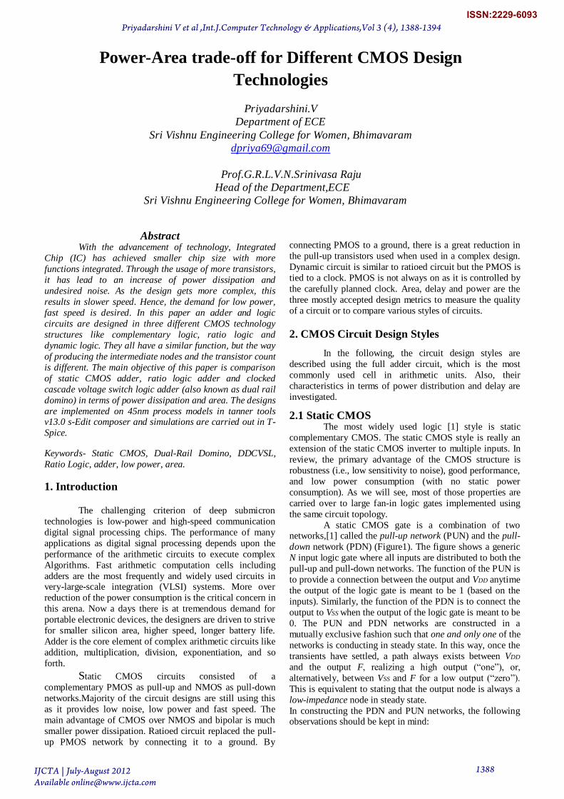
2.4.2 Pseudo NMOS Full adder
It consists of three inputs and two outputs.[5] In
our design, we have designated the three inputs as A, B and
CIN. The third input CIN represents carry input to the first
stage. The outputs are SUM and CARRY.[8] In this pseudo
NMOS technique we use only one PMOS transistor and the
input of PMOS transistor connected to ground potential.
Figure17 shows the Schematic diagram of a full adder.
Priyadarshini V et al ,Int.J.Computer Technology & Applications,Vol 3 (4), 1388-1394
IJCTA | July-August 2012 Available [email protected]
1392
ISSN:2229-6093
Figure17.Pseudo NMOS full adder circuit
3. Simulation Results: Output wave forms
3.1 Full Adder Circuits
The output wave forms of full adder circuits of
Static CMOS, Dual-Rail Domino and Pseudo NMOS which
are implemented using 45nm technology are simulated in
T-Spice simulator is as given below
3.1.1 Static Full Adder
Figure18. Output waveform of static full adder
3.1.2 Dual-Rail Domino full adder
Figure19. Output waveform of Dual-Rail Domino full adder
3.1.3 Pseudo NMOS full adder
Figure20. Output wave forms of Pseudo NMOS full adder
3.2 Logic Circuits
The output wave forms of logic circuits of Static
CMOS, Dual-Rail Domino and Pseudo NMOS which are
implemented using 45nm technology are simulated in T-
Spice simulator are given below
3.2.1 Static CMOS logic
Figure21. Output waveform of Static CMOS logic
Priyadarshini V et al ,Int.J.Computer Technology & Applications,Vol 3 (4), 1388-1394
IJCTA | July-August 2012 Available [email protected]
1393
ISSN:2229-6093
3.2.2 Dual-Rail Domino logic
Figure22. Output waveform of Dual-Rail domino logic
3.2.3 Pseudo NMOS logic
Figure23. Output waveform of Pseudo NMOS logic.
4. Simulation results: Area-Power
Area and Power of Static CMOS, Dual-Rail
Domino, Pseudo NMOS, DDCVS static and full adder
circuits are simulated using T-Spice simulator in 45nm
technology and the results are tabulated in below Table1.
Logic Circuit Area
( µm2
)
Power
(Watts)
Static CMOS 2112.5 5.247444e-006
Dual-Rail
Domino
2405.9 4.618738e-003
Pseudo NMOS 1912.3 4.318738e-003
Full adder
circuit
Area
( µm2 )
Power
(Watts)
Static CMOS 1681.7 2.275432e-003
Dual-Rail
Domino
1093.7 3.022191e-003
DDCVS 1052.5 1.702706e-003
Pseudo NMOS 992.7 0.1946289e-003
Table1. Area-Power results
5. Conclusion
In this paper various CMOS logic styles such as
Static CMOS logic, Dual-Rail Domino logic, DDCVS logic and Pseudo NMOS logic in various CMOS logic
gates such as AND, NAND, XOR, XNOR has been
implemented. A combinational circuit such as full adder
is implemented in various styles, power and area
calculations have been done. Among all the four
technique adders Pseudo NMOS has less area and less
power dissipation.
6. References
1. A Text book Neil HWESTE and Davis Harris ―CMOS VLSI DESIGN ―
a Circuit and Design Perspective
2. V Oklobdzijz R Montoya‖Design Performance Trade off in CMOS
Domino Logic‖ IEEE journal of solid state Circuit vol
121,PP:304-309,1986
3. Analysis and Comparison on Full Adder Block in Submicron
Technology Massimo Alioto, Member, IEEE, and Gaetano Palumbo, Senior Member, IEEE 4 Delay Uncertainty Due to Supply Variations in Static
and Dynamic Full Adders
4 .‖Cell Based Array for Deep submicron Technologies‖ by James Boe –
Kian Oey
5. A Text book Rene Van Leuken & Alexandar DeGraaf ―Designing
CMOS Circuits for Low Power‖
6. ―Mixed swing Quad rail for Low power dual rail domino logic‖ by
Bharath RaamSubramanian sun Microsystems.
7.‖Evaluation of high speed low voltage noise immune CMOS design
style‖thesis university of SIM by
8. Ding, L., & Mazumder, P. (2004). On Circuit Techniques to Improve
Noise Immunity of CMOS Dynamic Logic. IEEE TRANSACTIONS ON
VERY LARGE SCALE INTEGRATION (VLSI) SYSTEMS, VOL. 12, NO. 9
9 L. Heller et al., ―Cascade Voltage Switch Logic: A Differential CMOS
Logic Family,‖ Proc. IEEE ISSCC Conference, pp. 16–17, February 1984.
Priyadarshini V et al ,Int.J.Computer Technology & Applications,Vol 3 (4), 1388-1394
IJCTA | July-August 2012 Available [email protected]
1394
ISSN:2229-6093