power device packaging - department of...
TRANSCRIPT

Power Device Packaging
Zhenxian Liang
Oak Ridge National Laboratory
May 15, 2012
Project ID: APE023 This presentation does not contain any proprietary, confidential, or otherwise restricted information
2012 U.S. DOE Hydrogen and Fuel Cells Program and Vehicle Technologies Program Annual Merit Review and Peer Evaluation Meeting
2 Managed by UT-Battelle for the U.S. Department of Energy
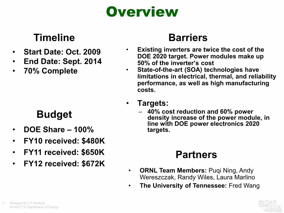
Overview
• Start Date: Oct. 2009 • End Date: Sept. 2014 • 70% Complete
• Existing inverters are twice the cost of the DOE 2020 target. Power modules make up 50% of the inverter’s cost
• State-of-the-art (SOA) technologies have limitations in electrical, thermal, and reliability performance, as well as high manufacturing costs.
• Targets: – 40% cost reduction and 60% power
density increase of the power module, in line with DOE power electronics 2020 targets. • DOE Share – 100%
• FY10 received: $480K • FY11 received: $650K • FY12 received: $672K
Timeline
Budget
Barriers
• ORNL Team Members: Puqi Ning, Andy Wereszczak, Randy Wiles, Laura Marlino
• The University of Tennessee: Fred Wang
Partners

3 Managed by UT-Battelle for the U.S. Department of Energy
Objective The fundamental efforts of this project are to: • Identify the limitations and shortcomings with existing device packaging
approaches; • Develop new packaging concepts for improved electrical, thermal
performance, manufacturability, and reliability; • Complement other power electronics research efforts within the Vehicle
Technology Program.
FY12 • Evaluate industry SOA power modules: Packaging performance, material,
processing and structure analysis. • Planar_Bond_All (PBA) power module development
Packaging process optimization: Material/structure, cost-effectiveness manufacturing.
Prototype module fabrication: Integration of advanced processing techniques.
Module testing and analysis: Electrical, thermal, properties measurement and analysis.
• Provide packaging support for other VTP APEEM projects: Fabrication of customer-specific power modules.

4 Managed by UT-Battelle for the U.S. Department of Energy
Milestone • Sept. 2011 - Selected advanced packaging candidate technologies. • Go No/Go Decision Point: Determine if prototype PBA
technology could potentially meet the performance and power density targets.
• Sept. 2012 -Test PBA modules to confirm improvements in electrical
and thermal performance. -Provide prototype modules for Segmented Drive
Inverter Project (APE004) and Wide Bandgap Project (APE003).
• Go/No Go – Determine if PBA modules can meet the targets on cost and reliability.

5 Managed by UT-Battelle for the U.S. Department of Energy
Approach Overall Strategy • Benchmark existing power device packaging technologies,
including package configuration, materials characterization, processing, and thermal and electrical performance evaluations. Determine the “weak links”.
• Develop new packaging approaches through simulation and experiments to improve power module electrical, thermal, thermo-mechanical performance and manufacturing cost-effectiveness.
• Apply packaging expertise to provide customer-specific power modules to VTP projects.
Status of Milestone • FY11 PBA prototype completed
• FY12 - PBA optimized module fabricated; Testing is underway;
- Customer modules delivered.

6 Managed by UT-Battelle for the U.S. Department of Energy
1.0E-3
1.0E-2
1.0E-1
1.0E+0
1.0E+1
0 1 2 3 4 5 6
Ther
mal
Tim
e C
onst
ant (
S)
Order Number
Prius_One_die
Prius_two_die
Infineon HP1
FY11/12 Technical Accomplishments Benchmark: Thermal Performance Characterization of SOA Modules
Infineon® HybridPack1™ under test
Thermal Resistance Comparison
Junction temperature cooling down curve Thermal model
Thermal Parameters
ToyotaPrius10_OneDie
ToyotaPrius10_TwoDie InfineonHP1 NissanLeaf
Thermal Resitance (C/W) 0.43 0.22 0.27 0.31Die area (10xcm2) 0.11 0.22 0.20 0.22Specific Thermal resitance
(Cm2.C/W) 0.47 0.49 0.54 0.68
00.10.20.30.40.50.60.70.8

7 Managed by UT-Battelle for the U.S. Department of Energy
0.44 mΩ
11.3 nH14.4 nH
Positive
7 mΩ19.6 nH
Negative
Neutral
7 mΩ19.6 nH
0.33 mΩ
0.17 mΩ0.18 mΩ7.3 nH 6.5 nH
0.44 mΩ11.3 nH14.4 nH
0.33 mΩ
0.17 mΩ0.18 mΩ7.3 nH 6.5 nH
0
50
100
150
200
250
300
350
400
0 0.5 1 1.5 2 2.5
Ice
(A)
Vce (V)
IGBT I-V Curve
P-side S-side
0
100
200
300
400
500
0
50
100
150
200
250
0 200 400 600 800 1000 1200
Volta
ge (V
)
Cur
rent
(A)
Time (nS)
Ice
Vce (S-Side)
Vce (P-Side)
IGBT Switching Curve
FY11/12 Technical Accomplishments Benchmark: Electrical Performance Characterization of SOA Modules
Nissan LEAF under Test
Prius 2010 Module 3_D Electromagnetic Model Lump element model of parasitic electric parameters

8 Managed by UT-Battelle for the U.S. Department of Energy
Die attach solder layer in Infineon HP1 Metallurgical compositions on top of IGBT die in Mitsubishi TPM_II
Insulator sheet in Nissan LEAF™ module Polyimide bond line
FY11/12 Technical Accomplishments Benchmark: Micro-structural analysis of packaging structures/materials

9 Managed by UT-Battelle for the U.S. Department of Energy
High power density integrated traction machine drive
Reduced stray inductance power module
Segmented drive Module HT Power SiC diode package.
Prototype: Customer-specific power modules FY11/12 Technical Accomplishments

10 Managed by UT-Battelle for the U.S. Department of Energy
Patent Pending: serial number 61/509312
Power Semiconductors stage
Integrated Advanced Cooler
Integrated Advanced Cooler
Planar_Bond_All Power Module Prototype
Planar Bond Power Stage Electrical Connection
FY11/12 Technical Accomplishments Develop: Planar_Bond_All power module
Advanced Power Module Concept
3-D planar Electrical Interconnection
Integrated, Double Sided Cooling
Symmetrically Mechanical Structure
Cost-effective Manufacture

11 Managed by UT-Battelle for the U.S. Department of Energy
Wire Bond Packaging
1 Substrate Preparation
3 Substrate Attach
2 Die Attach 4 Terminal Frame Attach
5 Wire Bond 6 Encapsulate 7 assembly
FY12 Technical Accomplishments Develop: Advanced manufacturing process
Patent Pending: serial number 61/509312
Planar_Bond_All
1st step: assembly
2nd step: heating profile
products

12 Managed by UT-Battelle for the U.S. Department of Energy
-400 -200 0 200 400 0
100
200
300
400
500
Time (ns)
Ice
(A),
Vce
(V),
P (W
/0.0
03),
E m
J/15
)
Ice Vce
Eoff
Poff
ToyotaPrius10 PlanarBondAllLp (nH) 50.3 12.8
Rp(0.1xmOhmic) 23.5 2.2
0
10
20
30
40
50
60
Electrical Parameters
Comparison
-600 -400 -200 0 200 400 600 0
50
100
150
200
250
300
350
400
450
500
Time (nS)
Vce(
V)
L: 45nH
30nH 20nH 15nH 10nH 5nH
FY12 Technical Accomplishments Develop: Analysis of electrical performance of PBA module
Lump element model of PBA module Parasitic parameters comparison
Simulation of IGBT switching Voltage overshoot vs. parasitic inductance

13 Managed by UT-Battelle for the U.S. Department of Energy
Inductance (nH) Experimental Value Calculated Value
Planar Bond_Lower IGBT 10.5 6.3
Wire Bond-Lower IGBT 31.9 23.5
0 100 200 300 400 500 600 0
20
40
60
80
100
120
140
160
180
Time(S)
Pow
er L
oss
(W)
Rp=0.22mΩ, P=1.030W Rp=2.35mΩ, P=11.08W
10
15
20
25
0 20 40 60 80
Eoff
(mJ)
Parasitic Inductance (nH)
X
X
Lp=10.5nH, Eoff=15.6mJ Lp=31.9nH, Eoff=17.2mJ
0
50
100
150
200
250
300
350
400
450
500
0
20
40
60
80
100
120
140
160
180
200
0 500 1000 1500 2000
Volta
ge (V
)
Cur
rent
(A)
Time (nS)
∆Vce(WB)=156V ∆Vce(PB)=72V
Ice Vce
FY12 Technical Accomplishments Develop: Analysis of electrical performance of PBA module
Comparison: PBA vs. wire bond module Voltage overshoot: PBA vs. wire bond
Switching loss: PBA vs. wire bond Conduction loss: PBA vs. wire bond

14 Managed by UT-Battelle for the U.S. Department of Energy
NissanLeaf ToyotaPrius10 PlanarBondAllSpecific Thermal resitance
(Cm2.C/W) 0.52 0.471 0.334
0
0.1
0.2
0.3
0.4
0.5
0.6
Thermal Resistance
θja,sp
29.1%
)($ ,
aj
spjaAreaDie
TTPS
kW −
•=∝
θη
FY11/12 Technical Accomplishments Develop: Analysis of thermal performance of PBA module
3-D Thermal Model of PBA module with mini-cooler Temperature distribution with cooling
PBA module under thermal test Measured Thermal parameter comparison

15 Managed by UT-Battelle for the U.S. Department of Energy
Ag Bonded DBC Substrates
Bond Line View After Tear Down
Cross sectional View of Bond Line
Bond Strength vs. Topography
FY12 Technical Accomplishments Develop: New bonding material and processing

16 Managed by UT-Battelle for the U.S. Department of Energy
Collaboration and Coordination • NREL
– Will use ORNL supplied modules to develop reliability parameters
• ORNL Materials Science and Technology Division – Leveraged DOE VTP Materials Program – Coordinated research to address packaging materials needs
• University of Tennessee – Assisted in benchmarking commercial packages
• Virginia Tech University – Collaborated on die attach material and power electronics module
packaging

17 Managed by UT-Battelle for the U.S. Department of Energy
Future Work – FY12 • Complete development of PBA processing
portfolio – Complete the die top electrode design and fabrication
process;
– Complete the insulation processing for solderable front metal (SFM) power semiconductor switches;
– Assemble all individual steps into one processing run;
– Finish the electrical and thermal performance tests. • Continue to benchmark packaging technologies
(performance, materials and processes) • Continue to support new power electronics module
development

18 Managed by UT-Battelle for the U.S. Department of Energy
Future Work – FY13 and Beyond • Enhance reliability of PBA concept
– Perform thermo-mechanical design and simulation of advanced planar bond module packages;
– Implement cost-effective materials and structures into PBA power modules;
– Conduct simulations and preliminary reliability tests of packages. • High temperature module packaging development
– Incorporate advanced bonding material/processing techniques; – Investigate new encapsulate, thermal materials; – Evaluate the high temperature effects of power module on cost,
efficiency and reliability, including Si, SiC and GaN power semiconductors.
• Continue to benchmark SOA technologies as needed (module performance, materials evaluation and processing)
• Provide packaging support for other projects

19 Managed by UT-Battelle for the U.S. Department of Energy
Summary • Developed PBA power module packaging technologies and
fabricated power modules resulting in, – Decreased package thermal resistance by 30%; – Decreased package parasitic electrical inductance by 3/4th, and electric
resistance by 90%; – Reduced the major packaging manufacturing steps from five (5) to two (2); – Achieved more than 30% volume, and weight reduction.
• Benchmarked SOA automotive power module – Nissan LEAF module: electrical, thermal test, insulator sheet analysis; – Toyota Prius 2010 module: thermal, and microstructure; – Infineon HybridPack1: thermal, and microstructure; – Mitsubishi TPM II: semiconductor and package microstructure.
• Delivered customer-specific power modules, – Segmented drive inverter modules (FY12); – HDITMD inverter modules (FY11); – High power SiC diode modules (FY12); – Low inductance wire bond modules (FY11).