power electronics (el-343) for t.e (el) books/pe.pdfpre-lab includes simulation of upcoming lab in...
TRANSCRIPT
PRACTICAL WORK BOOK
FOR ACADEMIC SESSION 2014
POWER ELECTRONICS
(EL-343) For T.E (EL)
Name:
Roll Number:
Batch:
Department:
Year:
Department of Electronic Engineering
N.E.D. University of Engineering & Technology, Karachi –75270, Pakistan
LABORATORY WORKBOOK
FOR THE COURSE
EL-343 POWER ELECTRONICS
Prepared By:
Saleha Bano ( Lecturer )
Reviewed By:
Dr. Usman Ali Shah (Assistant Professor)
Approved By:
The Board of Studies of Department of Electronic Engineering

PREFACE The basic theme behind designing this workbook is to give student a hands-on experience in
Power Electronic circuits. Assembling and soldering circuits which they studied theoretically
will help them to prove their concept about how practical circuits have direct dependence on
theoretical formulae.
Moreover, the tasks in beginning are kept simple, but their difficulty level has been increased in
direct proportion with labs. It will help to develop their analytical thinking about electronic
circuits and students should be able to unravel tight knots with a simple logic they have learnt. In
addition, pre-lab for each lab is also designed. Pre-lab includes simulation of upcoming lab in
Pspice, so that the students may able to infer the results of circuits before assembling and
soldering.
This workbook is designed to cover major portion of Power Electronic course. Labs 1 give an
introduction about Pspice. Lab 2 includes 1-phase half and full wave rectifier. Lab 3 and 4
represents same circuits but with controlled logic. In lab 5, students are introduced to 3-phase
uncontrolled rectifier circuits. Lab 6 and 7 represents how to control 3-phase rectifier circuits.
Lab 8, 9, 10 and 11 signify Choppers. And finally lab 12 deals with a design of a 1-phase Full
Bridge Inverter.

ACKNOWLEDGEMENT
I am indebted to the reviewer of this book who has given the valuable time in part or full to read
this book and provided useful suggestions. In particular, I would like to thank Mr. Shahzad
Siddique, Assistant Professor NEDUET for his constructive comments and valuable
propositions. I also wish to thank Mr. Ejaz Ahmed, Senior Instrumentation Technician NEDUET
for his critical ideas from his practical sense and positive approach to problem, whenever I got
trapped in circuits. I would also thank Mr. Ameer Abbas, Lab-Technician NEDUET, for
supporting me in assembling circuits and for the arrangements of power supplies and
components any time I wanted.
I wish to thank Mr. Ghaus Bakhsh, Professor NEDUET, who guided me at the start of this book
and given valuable suggestions that I carried alongside till completion of this book. I am grateful
to Mr. Shoaib Zaidi, Professor NEDUET, who continuously and sincerely supported me.

CONTENTS
Lab No.
Dated List of Experiments Page No.
Remarks
01. To become familiar with user interface of Pspice
02. To understand and design a circuit of 1-phase half
and full wave uncontrolled rectifier.
03. To understand and design a circuit of 1-phase half
wave controlled rectifier (0 to 90 degree).
04. To understand and design a circuit of 1-phase half
wave controlled rectifier (0 to 180 degree).
05. To understand and design a circuit of 1-phase full
wave controlled rectifier.
06. To understand and design a circuit of 3-phase half
wave uncontrolled rectifier.
07. To understand and design a circuit of 3-phase full
wave uncontrolled rectifier.
08. To understand and design a circuit of 3-phase half
wave controlled rectifier.
09. To understand and design a circuit of 3-phase full
wave controlled rectifier.
10. To understand and design a circuit of a Buck
converter.
11. To understand and design a circuit of a Boost
converter.
12. To understand and design a circuit of a Buck-
Boost converter.
13. To understand and design a circuit of Cuk
Converter.
14. To understand and design a circuit of a Single
Phase Full Bridge Inverter.

1
Lab. 01
An Introduction to Pspice
Objectives
The objective of this laboratory is to become familiar with user interface of Pspice.
Software Required
OrCAD v10.0
Introduction
Pspice is acronym for Personal Simulation Project with Integrated Circuit Emphasis. This software used for simulation of electronic circuits. It was first launched by Pspice itself but later on purchased by Orcad. Pspice gives very friendly and flexible user interface; it is therefore mostly recommended [1].
Launching a New Project
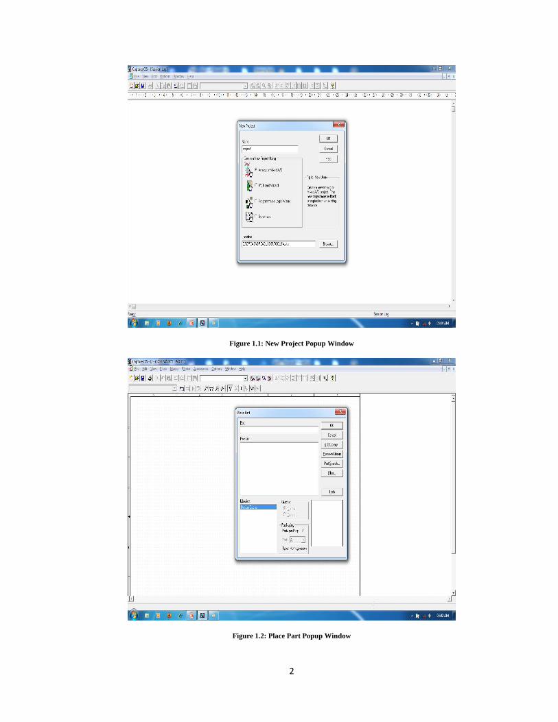
Click the icon of ‘Capture CIS’ in start menu; Capture CIS – Session log, screen will appear.
Go into the ‘File menu’, click ‘New’ and select ‘Project’; A pop-up window for new project will open as shown in figure 1.1.
Write name of project, select ‘Analog or Mixed A/D’ option in ‘Create a New Project Using’ and enter the location path for saving of current project.
Adding Libraries
A dotted screen will appear, which is your work area and a palette will appear on the right containing several options.
Click ‘Place Part’ button of palette on the right.
A window named place part will pop-up, showing nothing but ‘Design Cache’ in libraries as shown in figure 1.2.
Click ‘Add Library’ button at upper right corner of pop-up window.
Select all available libraries from Pspice folder and click open in order to include them for working.
It is a onetime procedure after installation of OrCAD.
2
Figure 1.1: New Project Popup Window
Figure 1.2: Place Part Popup Window

3
Figure 1.3: Added Libraries
Designing a Circuit
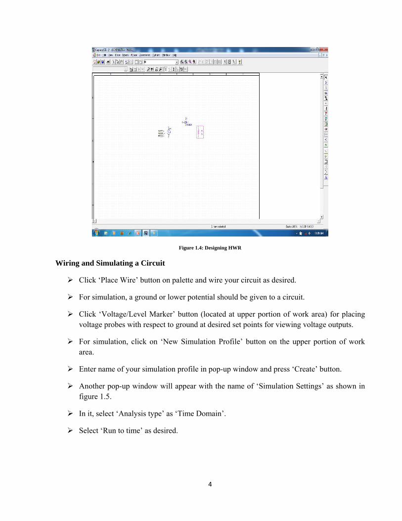
Now that libraries are included (as shown in figure 1.3), you are ready to kick off.
Let’s design ‘Half wave Rectifier’ (HWR).
The components required for HWR are, supply, diode and a load.
For source, click place part button on palette, select ‘SOURCE’ from libraries and select ‘VSIN’ from part list.
Assign values to VOFF, VAMP and FREQ (by a double click on each parameter) in ‘Display Properties’ window.
For diode, again click place part button in palette, select ‘DIODE’ from libraries and select ‘D1N4001’ from part list.
For load, click place part button in palette, select ‘ANALOG’ from libraries and select ‘R’ from part list. Figure 1.4 shows components placed on work area.
4
Figure 1.4: Designing HWR
Wiring and Simulating a Circuit
Click ‘Place Wire’ button on palette and wire your circuit as desired.
For simulation, a ground or lower potential should be given to a circuit.
Click ‘Voltage/Level Marker’ button (located at upper portion of work area) for placing voltage probes with respect to ground at desired set points for viewing voltage outputs.
For simulation, click on ‘New Simulation Profile’ button on the upper portion of work area.
Enter name of your simulation profile in pop-up window and press ‘Create’ button.
Another pop-up window will appear with the name of ‘Simulation Settings’ as shown in figure 1.5.
In it, select ‘Analysis type’ as ‘Time Domain’.
Select ‘Run to time’ as desired.

5
Figure 1.5: Simulation Settings Popup Window
If you want to zoom in the curve, select ‘Run to time’ = 1/f or smaller than 1/f (where f is the input frequency).
If you want to zoom out the curve, select ‘Run to time’ greater than 1/f (where f is the input frequency).
Click the ‘Run Pspice’ button in order to simulate your circuit.
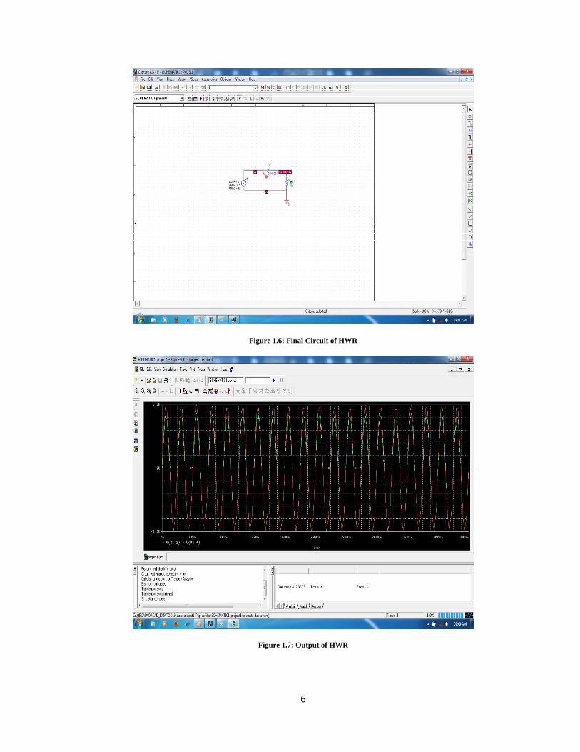
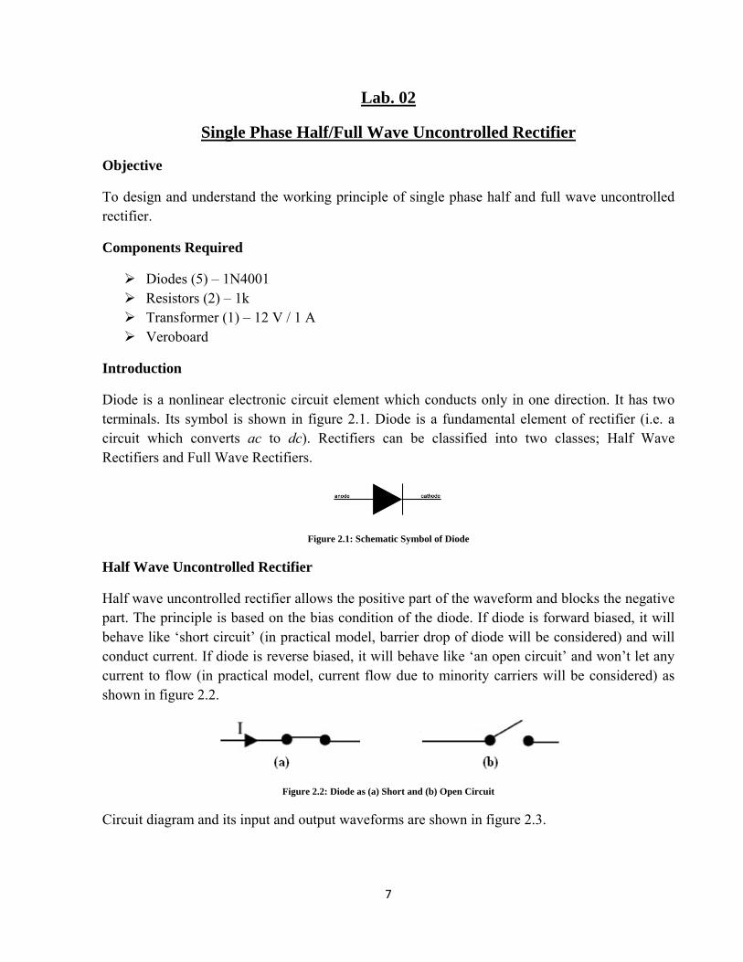
The final circuit and its output is shown in figure 1.6 and figure 1.7.
Task
Design Single Phase Half wave Rectifier (uncontrolled) on Pspice.
Design Single Phase Full wave Rectifier (uncontrolled) on Pspice.
Reference
[1] Abbreviation for Personal Simulation Project with Integrated Circuit Emphasis (Updated on 28 December 2011; accessed on 09 January 2012). Available from http://en.wikipedia.org/wiki/PSpice
6
17
Figure 1.6: Final Circuit of HWR
Figure 1.7: Output of HWR
7
Lab. 02
Single Phase Half/Full Wave Uncontrolled Rectifier
Objective
To design and understand the working principle of single phase half and full wave uncontrolled rectifier.
Components Required
Diodes (5) – 1N4001 Resistors (2) – 1k Transformer (1) – 12 V / 1 A Veroboard
Introduction
Diode is a nonlinear electronic circuit element which conducts only in one direction. It has two terminals. Its symbol is shown in figure 2.1. Diode is a fundamental element of rectifier (i.e. a circuit which converts ac to dc). Rectifiers can be classified into two classes; Half Wave Rectifiers and Full Wave Rectifiers.
Figure 2.1: Schematic Symbol of Diode
Half Wave Uncontrolled Rectifier
Half wave uncontrolled rectifier allows the positive part of the waveform and blocks the negative part. The principle is based on the bias condition of the diode. If diode is forward biased, it will behave like ‘short circuit’ (in practical model, barrier drop of diode will be considered) and will conduct current. If diode is reverse biased, it will behave like ‘an open circuit’ and won’t let any current to flow (in practical model, current flow due to minority carriers will be considered) as shown in figure 2.2.
Figure 2.2: Diode as (a) Short and (b) Open Circuit
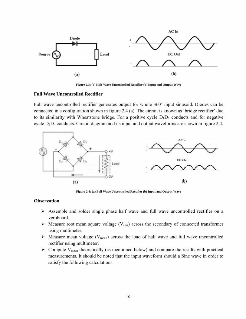
Circuit diagram and its input and output waveforms are shown in figure 2.3.
8
Figure 2.3: (a) Half Wave Uncontrolled Rectifier (b) Input and Output Wave
Full Wave Uncontrolled Rectifier
Full wave uncontrolled rectifier generates output for whole 360o input sinusoid. Diodes can be connected in a configuration shown in figure 2.4 (a). The circuit is known as ‘bridge rectifier’ due to its similarity with Wheatstone bridge. For a positive cycle D1D2 conducts and for negative cycle D3D4 conducts. Circuit diagram and its input and output waveforms are shown in figure 2.4.
Figure 2.4: (a) Full Wave Uncontrolled Rectifier (b) Input and Output Wave
Observation
Assemble and solder single phase half wave and full wave uncontrolled rectifier on a veroboard.
Measure root mean square voltage (Vrms) across the secondary of connected transformer using multimeter.
Measure mean voltage (Vmean) across the load of half wave and full wave uncontrolled rectifier using multimeter.
Compute Vmean theoretically (as mentioned below) and compare the results with practical measurements. It should be noted that the input waveform should a Sine wave in order to satisfy the following calculations.

9
For Half Wave:
(1)
(2)
(3)
For Full Wave:
(4)
(5)
(6)
Where, Vrms is the voltage measured across secondary of the transformer, Vp is the peak value of voltage, Vmean is the average value of voltage measured across load and Vd is the diode’s barrier potential measured across it.
Calculation
For Half Wave:

10
For Full Wave:
Task
Design a circuit for controlling the firing angle of SCR (90o) used in Single Phase Half Wave Controlled Rectifier with the help of a Resistive circuit.
11
Lab. 03
1-Phase Half Wave Controlled Rectifier (0 to 90 degree)
Objective
To understand and design a circuit for 1-phase half wave controlled rectifier from 0 to 90 degree.
Components Required
SCR (1) – C106 Diodes (2) – 1N4001 Transformer (1) – 12 V / 1A Resistor (1) – 1K / 1/22Watt Pot. (1) – 50k Veroboard
Introduction
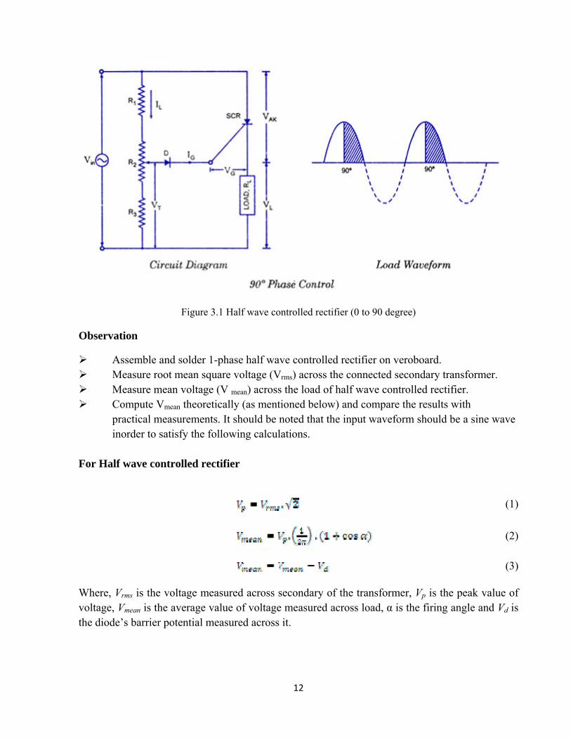
In ac circuits, the SCR can be turned on by the gate at any angle a with respect to the applied voltage. This angle α is called the firing angle. Power control is obtained by varying the firing angle and this is known as phase control. In the phase-control circuit given in fig. 1, the gate triggering voltage is derived from the ac supply through resistors R1, R2 and R3. The variable resistance R2 limits the gate current during positive half cycles of the supply. If the moving contact is set to the top of resistor R2, resistance in the circuit is the lowest and the SCR may trigger almost immediately at the commencement of the positive half cycle of the input. If, on the other hand, the moving contact is set to the bottom of resistor R2, resistance in the circuit is maximum, the SCR may not switch on until the peak of the positive half-cycle. By adjusting R2 between these two extremes, SCR can be switched on somewhere between the commencement and peak of the positive half-cycle, that is between 0° and 90°. If the triggering voltage VT is not large enough to trigger SCR at 90°, the device will not trigger on at all, because VT has the maximum value at the peak of the input and decreases with the fall in voltage. This operation is sometimes referred to as half-wave variable-resistance phase control. It is an effective method of controlling the load power.
Diode D is provided to protect the SCR gate from the negative voltage that would otherwise be applied during the negative half cycle of the input. It can be seen from the circuit diagram shown in fig.3.1, that at the instant of turning on of the SCR gate current flows through RL and diode. So
VT=VD + VG + IGRL
12
Figure 3.1 Half wave controlled rectifier (0 to 90 degree)
Observation
Assemble and solder 1-phase half wave controlled rectifier on veroboard. Measure root mean square voltage (Vrms) across the connected secondary transformer. Measure mean voltage (V mean) across the load of half wave controlled rectifier. Compute Vmean theoretically (as mentioned below) and compare the results with
practical measurements. It should be noted that the input waveform should be a sine wave inorder to satisfy the following calculations. For Half wave controlled rectifier
(1)
(2)
(3)
Where, Vrms is the voltage measured across secondary of the transformer, Vp is the peak value of voltage, Vmean is the average value of voltage measured across load, α is the firing angle and Vd is the diode’s barrier potential measured across it.

13
Calculation
For Half wave controlled rectifier (0 to 90 degree)
Task
Design a circuit for controlling the firing angle of SCR (180 degree) used in single phase Half wave rectifier with the help of RC circuit.
14
Lab. 04
1-Phase Half Wave Controlled Rectifier (0 to 180 degree)
Objective
Understand and design a circuit for 1-phase half wave controlled rectifier.
Components Required
SCR (1) – C106 Diodes (2) – 1N4001 Capacitor (1) – 1uF / 50V Transformer (1) – 12 V / 1A Resistor (1) – 1K / 1/2Watt Pot. (1) – 50k Veroboard
Introduction
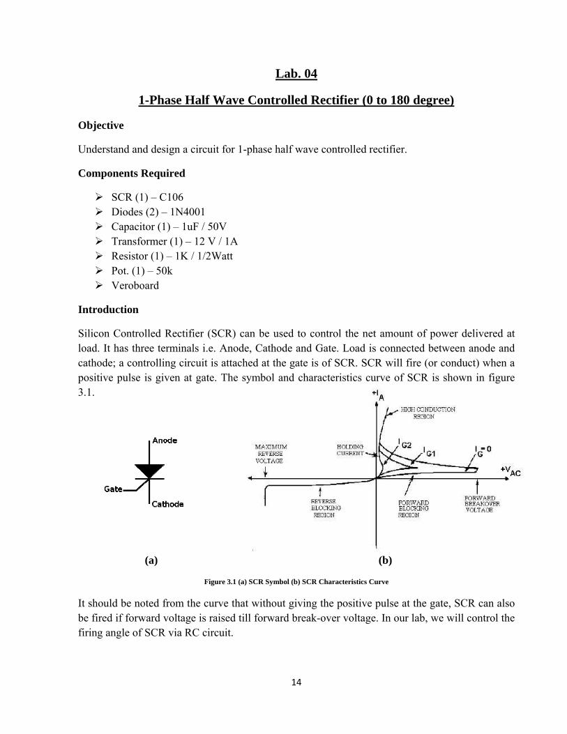
Silicon Controlled Rectifier (SCR) can be used to control the net amount of power delivered at load. It has three terminals i.e. Anode, Cathode and Gate. Load is connected between anode and cathode; a controlling circuit is attached at the gate is of SCR. SCR will fire (or conduct) when a positive pulse is given at gate. The symbol and characteristics curve of SCR is shown in figure 3.1.
(a) (b)
Figure 3.1 (a) SCR Symbol (b) SCR Characteristics Curve
It should be noted from the curve that without giving the positive pulse at the gate, SCR can also be fired if forward voltage is raised till forward break-over voltage. In our lab, we will control the firing angle of SCR via RC circuit.

15
Half Wave Controlled Rectifier (HWCR)
HWCR can be designed as shown in figure 3.2. The circuit represents basic configuration of half wave rectifier, apart from diode replaced with SCR. For the positive half of input sinusoid SCR will be forward biased and requires a positive pulse at gate to conduct current (or to be triggered).
Figure 3.2: 1-Phase Half Wave Controlled Rectifier
RC time constant of capacitor is stabled in such a way that SCR should fire at required angle. ‘R’ can be varied to change the firing angle of SCR. The circuit diagram is shown in figure 3.3. For negative half; SCR will be reverse biased and won’t conduct.
Figure 3.3: 1-Phase HWCR with RC Gate Controlling Circuit
Observation
Assemble and solder 1-phase half wave controlled rectifier on veroboard. Measure root mean square voltage (Vrms) across the secondary of connected transformer. Measure mean voltage (Vmean) across the load of half wave controlled rectifier. Compute Vmean theoretically (as mentioned below) and compare the results with practical
measurements. It should be noted that the input waveform should be a Sine wave in order to satisfy the following calculations.

16
For Half Wave Controlled Rectifier
(1)
(2)
(3)
Where, Vrms is the voltage measured across secondary of the transformer, Vp is the peak value of voltage, Vmean is the average value of voltage measured across load, α is the firing angle and Vd is the diode’s barrier potential measured across it.
Calculation
For Half Wave Controlled Rectifier (0 to 180 degree)
Task
Simulate a circuit for 1-phase controlled full wave rectifier on Pspice. Simulate a circuit that controls the triggering of Uni-junction Transistor (UJT) at different
time intervals on Pspice.
17
Lab. 05
1-Phase Full Wave Controlled Rectifier
Objective
Understand and design a circuit of 1-phase full wave controlled rectifier.
Components Required
SCR (2) – C106 Diodes (8) – 1N4001-7 UJT (1) - 2N2646 Resistors - (1)470 ohms / 1 watt, (1)5.6 Kohms / 1 watt, (1)270 ohms / 1 watt, (2)15 ohms
/ 1 watt, (2)1 Kohms / 1 watt, (1)100 ohms / 10 watt Capacitor (1) - 82nF / 50 volts or greater Zener Diode (1) - 12 volts / 1 watt Pot. (1) - 100k Veroboard
Introduction
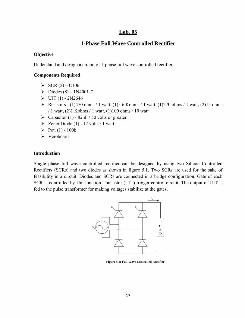
Single phase full wave controlled rectifier can be designed by using two Silicon Controlled Rectifiers (SCRs) and two diodes as shown in figure 5.1. Two SCRs are used for the sake of feasibility in a circuit. Diodes and SCRs are connected in a bridge configuration. Gate of each SCR is controlled by Uni-junction Transistor (UJT) trigger control circuit. The output of UJT is fed to the pulse transformer for making voltages stabilize at the gates.
Figure 5.1: Full Wave Controlled Rectifier
18
1-Phase Full Wave Controlled Rectifier
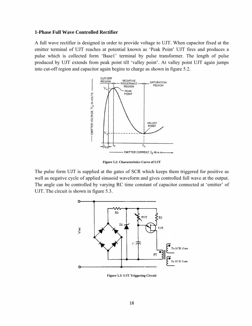
A full wave rectifier is designed in order to provide voltage to UJT. When capacitor fixed at the emitter terminal of UJT reaches at potential known as ‘Peak Point’ UJT fires and produces a pulse which is collected form ‘Base1’ terminal by pulse transformer. The length of pulse produced by UJT extends from peak point till ‘valley point’. At valley point UJT again jumps into cut-off region and capacitor again begins to charge as shown in figure 5.2.
Figure 5.2: Characteristics Curve of UJT
The pulse form UJT is supplied at the gates of SCR which keeps them triggered for positive as well as negative cycle of applied sinusoid waveform and gives controlled full wave at the output. The angle can be controlled by varying RC time constant of capacitor connected at ‘emitter’ of UJT. The circuit is shown in figure 5.3.
Figure 5.3: UJT Triggering Circuit

19
Observation
Assemble and solder 1-phase full wave controlled rectifier on veroboard. Measure root mean square voltage (Vrms) across the secondary of connected transformer. Measure mean voltage (Vmean) across the load of full wave controlled rectifier. Compute Vmean theoretically at different angles (as mentioned below) and compare the
results with practical measurements. It should be noted that the input waveform should be a Sine wave in order to satisfy the following calculations.
For Full Wave Controlled Rectifier
(1)
(2)
(3)
Where, Vrms is the voltage measured across secondary of the transformer, Vp is the peak value of voltage, Vmean is the average value of voltage measured across load, α is the firing angle and Vd is the diode’s barrier potential measured across it.
Calculation
For Full Wave Controlled Rectifier
Task
Simulate the circuit of 3-phase half wave uncontrolled rectifier in Pspice.
20
Lab. 06
3-Phase Half Wave Uncontrolled Rectifier
Objective
To understand and design the working principle of 3-phase half wave uncontrolled rectifier.
Components Required
Diodes (6) – 1N4001--7 Resistor (2) – 1 Kohm m / ½ or 1 watt Transformer (3) – 12 volt / 1 A Veroboard
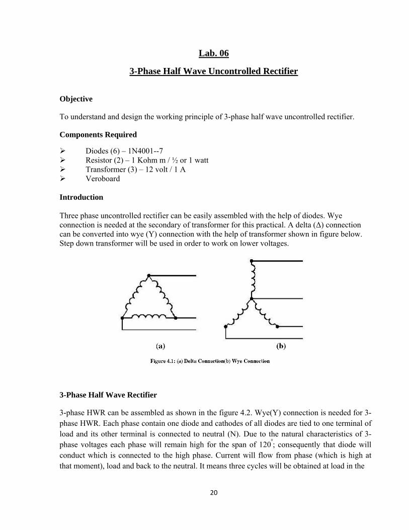
Introduction Three phase uncontrolled rectifier can be easily assembled with the help of diodes. Wye connection is needed at the secondary of transformer for this practical. A delta (Δ) connection can be converted into wye (Y) connection with the help of transformer shown in figure below. Step down transformer will be used in order to work on lower voltages.
3-Phase Half Wave Rectifier
3-phase HWR can be assembled as shown in the figure 4.2. Wye(Y) connection is needed for 3-phase HWR. Each phase contain one diode and cathodes of all diodes are tied to one terminal of load and its other terminal is connected to neutral (N). Due to the natural characteristics of 3-phase voltages each phase will remain high for the span of 120
0
; consequently that diode will conduct which is connected to the high phase. Current will flow from phase (which is high at that moment), load and back to the neutral. It means three cycles will be obtained at load in the
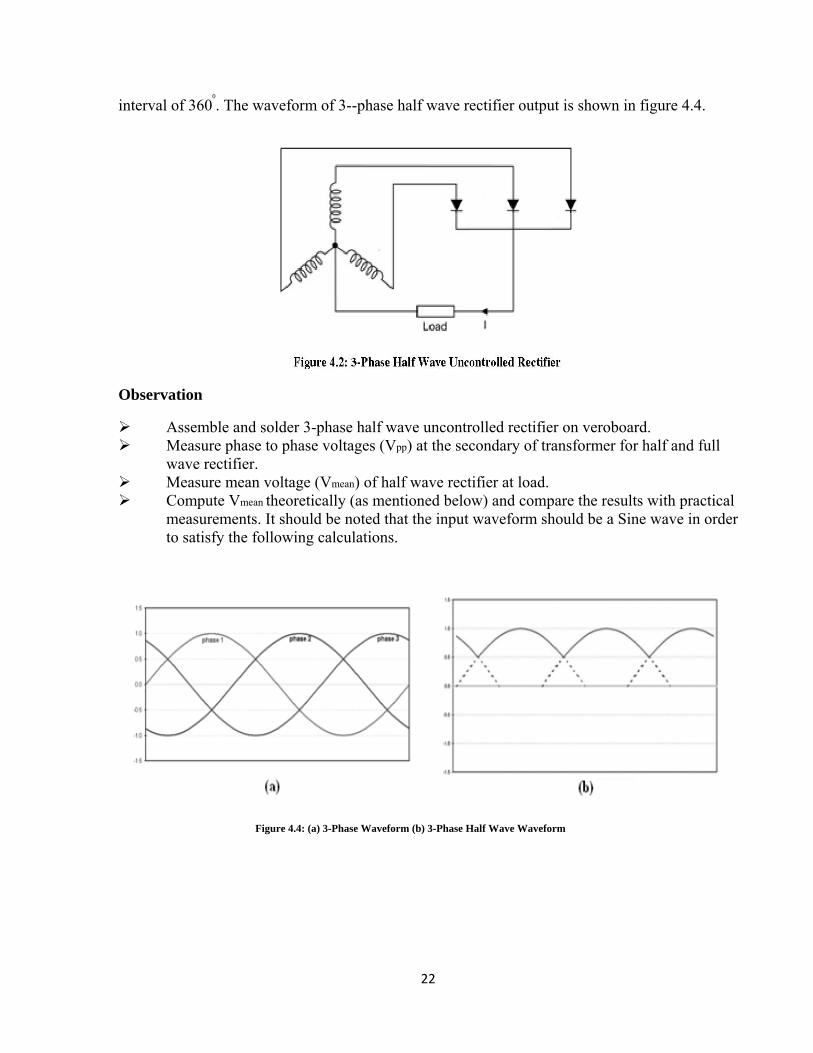
22
interval of 3600
. The waveform of 3--phase half wave rectifier output is shown in figure 4.4.
Observation
Assemble and solder 3-phase half wave uncontrolled rectifier on veroboard. Measure phase to phase voltages (Vpp) at the secondary of transformer for half and full
wave rectifier. Measure mean voltage (Vmean) of half wave rectifier at load. Compute Vmean theoretically (as mentioned below) and compare the results with practical
measurements. It should be noted that the input waveform should be a Sine wave in order to satisfy the following calculations.
Figure 4.4: (a) 3-Phase Waveform (b) 3-Phase Half Wave Waveform

23
For 3-Phase Half Wave Uncontrolled Rectifier
(1)
(2)
(3)
(4)
Where, Vpp is the phase to phase voltage, Vpn is the phase to neutral voltage calculated from phase to phase voltage, Vpeak is the peak value of phase to neutral voltage, Vmean is the average value of voltage and Vd is the diode’s barrier potential measured across it.

1
Calculation
For 3-Phase Half Wave Uncontrolled Rectifier
Task
Simulate 3-Phase Full Wave UnControlled Rectifier using Pspice.
2
Lab. 07
3-Phase Full Wave Uncontrolled Rectifier
Objective
To design and understand the working principle of 3-phase full wave uncontrolled rectifier.
Components Required
Diodes (9) – 1N4001-7 Resistor (2) – 1 Kohm / ½ or 1 watt Transformer (3) – 12 volt / 1 A Veroboard
Introduction
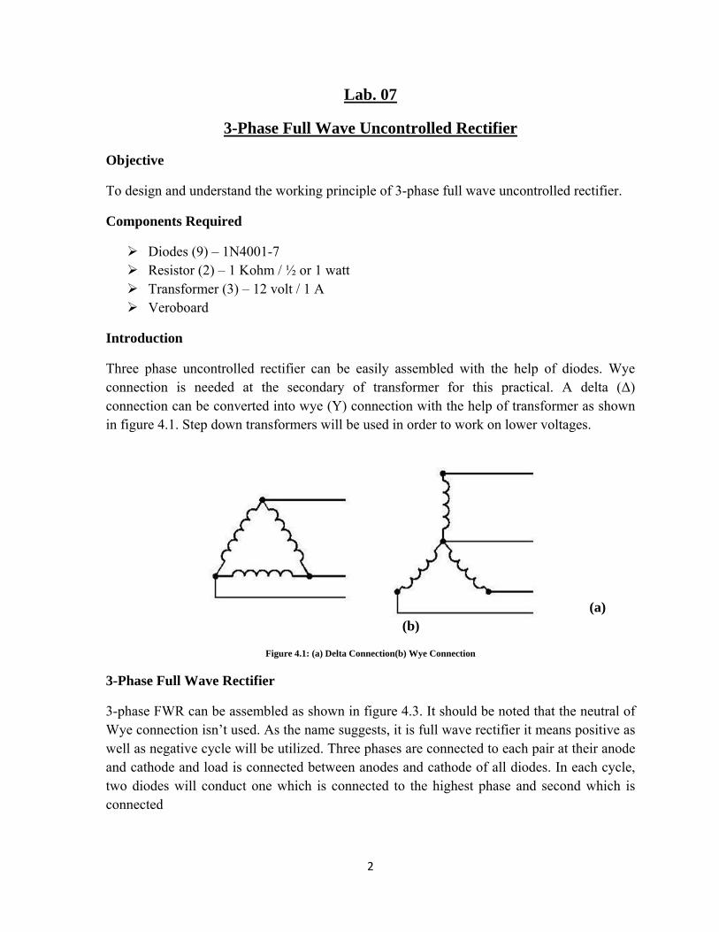
Three phase uncontrolled rectifier can be easily assembled with the help of diodes. Wye connection is needed at the secondary of transformer for this practical. A delta (Δ) connection can be converted into wye (Y) connection with the help of transformer as shown in figure 4.1. Step down transformers will be used in order to work on lower voltages.
(a) (b)
Figure 4.1: (a) Delta Connection(b) Wye Connection
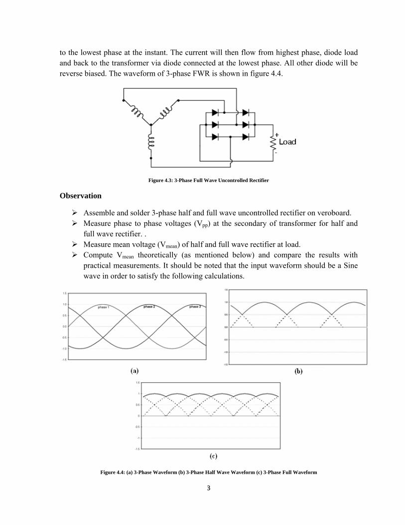
3-Phase Full Wave Rectifier
3-phase FWR can be assembled as shown in figure 4.3. It should be noted that the neutral of Wye connection isn’t used. As the name suggests, it is full wave rectifier it means positive as well as negative cycle will be utilized. Three phases are connected to each pair at their anode and cathode and load is connected between anodes and cathode of all diodes. In each cycle, two diodes will conduct one which is connected to the highest phase and second which is connected
3
to the lowest phase at the instant. The current will then flow from highest phase, diode load and back to the transformer via diode connected at the lowest phase. All other diode will be reverse biased. The waveform of 3-phase FWR is shown in figure 4.4.
Figure 4.3: 3-Phase Full Wave Uncontrolled Rectifier
Observation
Assemble and solder 3-phase half and full wave uncontrolled rectifier on veroboard. Measure phase to phase voltages (Vpp) at the secondary of transformer for half and
full wave rectifier. . Measure mean voltage (Vmean) of half and full wave rectifier at load. Compute Vmean theoretically (as mentioned below) and compare the results with
practical measurements. It should be noted that the input waveform should be a Sine wave in order to satisfy the following calculations.
Figure 4.4: (a) 3-Phase Waveform (b) 3-Phase Half Wave Waveform (c) 3-Phase Full Waveform

4
For 3-phase Full Wave Uncontrolled Rectifier
(1)
(2)
(3)
(4)
Where, Vpp is the phase to phase voltage, Vpn is the phase to neutral voltage calculated from phase to phase voltage, Vpeak is the peak value of phase to neutral voltage, Vmean is the average value of voltage and Vd is the diode’s barrier potential measured across it.
Calculation
For 3-Phase Full Wave Uncontrolled Rectifier
Task
Simulate 3-phase half wave controlled rectifier using UJT as triggering circuit in Pspice.
5
Lab. 08
3-Phase Half Wave Controlled Rectifier
Objective
To design and understand the working principle of 3-phase half wave controlled rectifier.
Components Required
UJT Firing Circuit SCR (3) – C106 Resistor (4) – (3) 1 Kohm / ¼ watt; 100 ohm 10 watt (load); NPN Transistor (3) – 2N2222 or as desired. Pulse Transformer (3) – Solo Package or as desired. Veroboard
Introduction
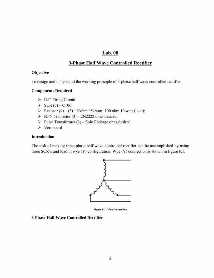
The task of making three phase half wave controlled rectifier can be accomplished by using three SCR’s and load in wye (Y) configuration. Wye (Y) connection is shown in figure 6.1.
Figure 6.1: Wye Connection
3-Phase Half Wave Controlled Rectifier
6
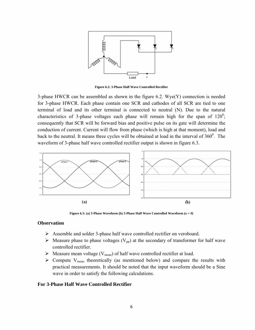
Figure 6.2: 3-Phase Half Wave Controlled Rectifier
3-phase HWCR can be assembled as shown in the figure 6.2. Wye(Y) connection is needed for 3-phase HWCR. Each phase contain one SCR and cathodes of all SCR are tied to one terminal of load and its other terminal is connected to neutral (N). Due to the natural characteristics of 3-phase voltages each phase will remain high for the span of 1200; consequently that SCR will be forward bias and positive pulse on its gate will determine the conduction of current. Current will flow from phase (which is high at that moment), load and back to the neutral. It means three cycles will be obtained at load in the interval of 3600. The waveform of 3-phase half wave controlled rectifier output is shown in figure 6.3.
Figure 6.3: (a) 3-Phase Waveform (b) 3-Phase Half Wave Controlled Waveform (α = 0)
Observation
Assemble and solder 3-phase half wave controlled rectifier on veroboard. Measure phase to phase voltages (Vpp) at the secondary of transformer for half wave
controlled rectifier. Measure mean voltage (Vmean) of half wave controlled rectifier at load. Compute Vmean theoretically (as mentioned below) and compare the results with
practical measurements. It should be noted that the input waveform should be a Sine wave in order to satisfy the following calculations.
For 3-Phase Half Wave Controlled Rectifier

7
(1)
(2)
(3)
(4)
Where, Vpp is the phase to phase voltage, Vpn is the phase to neutral voltage calculated from phase to phase voltage, Vpeak is the peak value of phase to neutral voltage, Vmean is the average value of voltage, α is the firing angle and Vd is the diode’s barrier potential measured across it.
Calculation
For 3-Phase Half Wave Controlled Rectifier
8
Task
Simulate 3-phase full wave controlled rectifier using UJT as triggering circuit in Pspice.
Lab. 09
3-Phase Full Wave Controlled Rectifier
Objective
To design and understand the working principle of 3-phase full wave controlled rectifier.
Components Required
UJT Firing Circuit SCR (3) – C106 Diodes (3) – 1N4001-7 Resistor (4) – (3) 1 Kohm / ¼ watt; 100 ohm 10 watt (load) NPN Transistor (3) – 2N2222 or as desired. Pulse Transformer (3) – Solo Package or as desired. Veroboard
Introduction
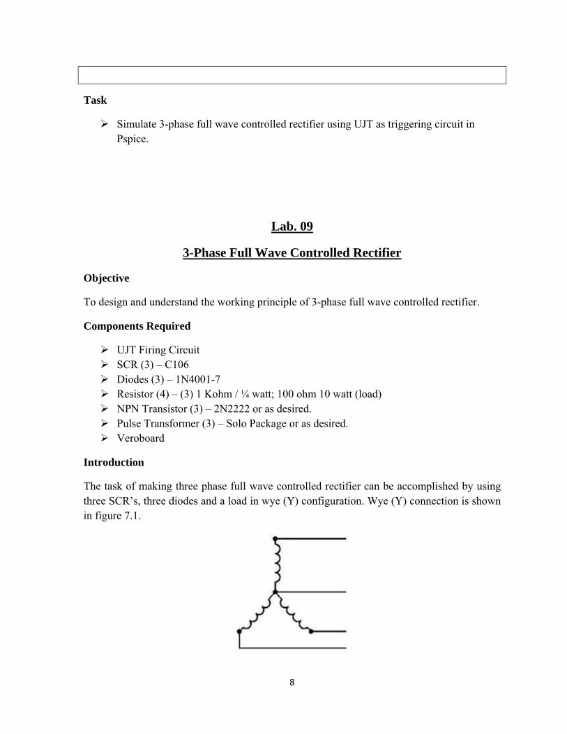
The task of making three phase full wave controlled rectifier can be accomplished by using three SCR’s, three diodes and a load in wye (Y) configuration. Wye (Y) connection is shown in figure 7.1.
9
Figure 7.1: Wye Connection
3-Phase Full Wave Controlled Rectifier
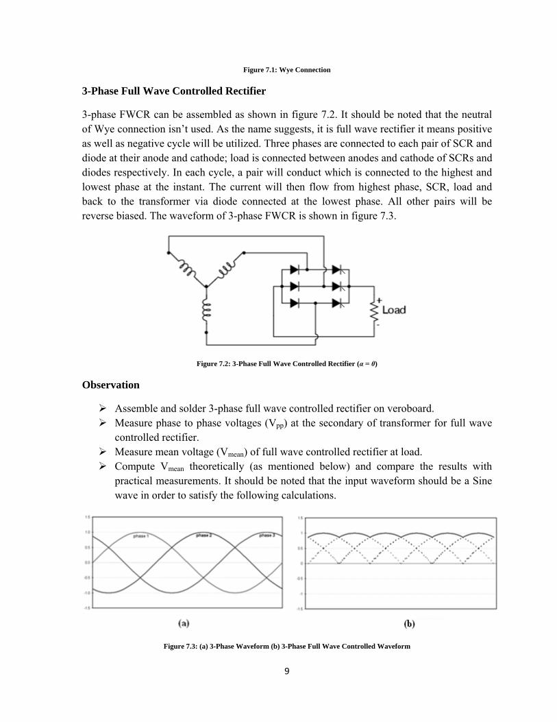
3-phase FWCR can be assembled as shown in figure 7.2. It should be noted that the neutral of Wye connection isn’t used. As the name suggests, it is full wave rectifier it means positive as well as negative cycle will be utilized. Three phases are connected to each pair of SCR and diode at their anode and cathode; load is connected between anodes and cathode of SCRs and diodes respectively. In each cycle, a pair will conduct which is connected to the highest and lowest phase at the instant. The current will then flow from highest phase, SCR, load and back to the transformer via diode connected at the lowest phase. All other pairs will be reverse biased. The waveform of 3-phase FWCR is shown in figure 7.3.
Figure 7.2: 3-Phase Full Wave Controlled Rectifier (α = 0)
Observation
Assemble and solder 3-phase full wave controlled rectifier on veroboard. Measure phase to phase voltages (Vpp) at the secondary of transformer for full wave
controlled rectifier. Measure mean voltage (Vmean) of full wave controlled rectifier at load. Compute Vmean theoretically (as mentioned below) and compare the results with
practical measurements. It should be noted that the input waveform should be a Sine wave in order to satisfy the following calculations.
Figure 7.3: (a) 3-Phase Waveform (b) 3-Phase Full Wave Controlled Waveform

10
For 3-phase Full Wave Uncontrolled Rectifier
(1)
(2)
(3)
(4)
Where, Vpp is the phase to phase voltage, Vpn is the phase to neutral voltage calculated from phase to phase voltage, Vpeak is the peak value of phase to neutral voltage, Vmean is the average value of voltage, α is the firing angle and Vd is the diode’s barrier potential measured across it.
Calculation
For 3-Phase Full Wave Controlled Rectifier
Task

11
Simulate Buck Converter in Pspice.
Lab. 10
Buck Converter
Objective
To understand and design the working principle of a Buck converter.
Components Required
� IC - 555 timer (1)
� Capacitors - 0.1 uF (2), 0.01 uF(1), 100 uF(1)
� Resistors - 100 K Pot. (1), 10 k (1), 1 k (2) � Diodes - 1N4001-7 / 1N5818 (2)
� Inductor - You can use Pulse Transformer windings
� Transistor - 2N2222 (2)
� Veroboard
Introduction
Converter is a generic word, commonly used for indicating the type of voltage and current
conversion in the field of power electronics. Generally, four types of converters are
discussed.
� AC – AC Converter (a.k.a. Transformers)
� AC – DC Converter (a.k.a. Rectifiers)
� DC – AC Converter (a.k.a. Inverters)
� DC – DC Converter (a.k.a. Choppers)
The scope of this lab won’t allow us to discuss all four converters in detail, rather we will
concentrate on DC – DC Converter (i.e. Choppers). Choppers are classified into two
operations; Step Down and Step Up operation. As name infer, step down converter converts
higher mean voltages to the lower mean voltages and step up converter converts lower mean
voltage to the higher ones. There are typically four types of chopper which are classified on
the basis of their operation.
� Buck Converter
� Boost Converter
� Buck-Boost Converter
� CÚk Converter
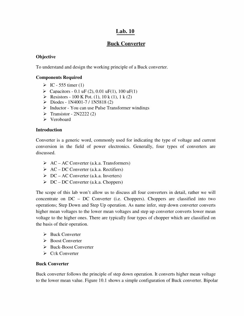
Buck Converter
Buck converter follows the principle of step down operation. It converts higher mean voltage
to the lower mean value. Figure 10.1 shows a simple configuration of Buck converter. Bipolar
junction transistor (npn) can be used as switch. Through analytical analysis, we came across
a formula which this follows i.e.
�# � %. �$ (1)
Where, Vo represents the output mean voltage, Vs represents input mean voltage and K
represents the duty cycle.
Figure 10.1: Buck Converter
It means that if we somehow generate a waveform that’s ON or OFF can be control; we will
manage to control the output variable. Where, output variable is directly proportional to the
duty cycle. Duty cycle can be generated with the help of Comparator or Astable multi-
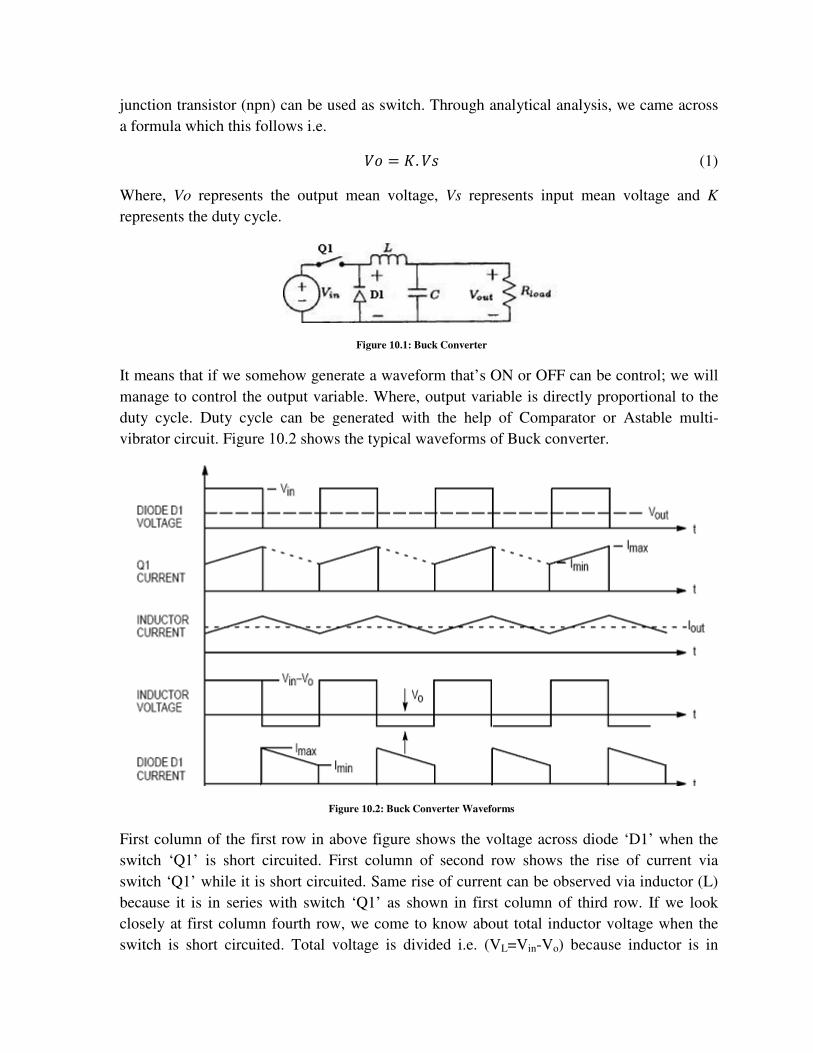
vibrator circuit. Figure 10.2 shows the typical waveforms of Buck converter.
Figure 10.2: Buck Converter Waveforms
First column of the first row in above figure shows the voltage across diode ‘D1’ when the
switch ‘Q1’ is short circuited. First column of second row shows the rise of current via
switch ‘Q1’ while it is short circuited. Same rise of current can be observed via inductor (L)
because it is in series with switch ‘Q1’ as shown in first column of third row. If we look
closely at first column fourth row, we come to know about total inductor voltage when the
switch is short circuited. Total voltage is divided i.e. (VL=Vin-Vo) because inductor is in

series with load. Finally, first column of the last row show the current via diode is equal to
zero because diode is reverse biased when switch is short circuited.
Why Buck Converter when Regulator are Available?
Regulators also perform the same operation as Buck converters i.e. step down DC voltage to
the desired level. But they dissipate excess amount of energy in the form of heat as they
operate. Buck converters, on the other hand, are 95% efficient as compared with their
counterparts.
Observation
� Assemble and solder Astable multi-vibrator and Buck Converter on veroboard.
� Fix duty cycle of switch at zero and measure Vmean across load.
� Fix duty cycle of switch at 50% and measure Vmean across load.
� Fix duty cycle of switch at 100% and measure Vmean across load.
� Compute Vmean theoretically (as mentioned below) and compare the results with
practical measurements.
For Buck Converter
�# � %. �$
Where, Vo represents the output mean voltage, Vs represents input mean voltage and K
represents the duty cycle.
Calculation
For Buck Converter

� Explain the second column of each row figure in fig. 10.2.
_____________________________________________________________________
_____________________________________________________________________
_____________________________________________________________________
_____________________________________________________________________
_____________________________________________________________________
_____________________________________________________________________
Task
� Simulate Boost Converter in Pspice.
Lab. 11
Boost Converter
Objective
To understand and design the working principle of a Boost converter.
Components Required
� IC - 555 timer (1)
� Capacitors - 0.1 uF (2), 0.01 uF(1), 100 uF(1)
� Resistors - 100 K Pot. (1), 10 k (1), 1 k (2)
� Diodes - 1N4001-7 / 1N5818 (2) � Inductor - You can use Pulse Transformer windings
� Transistor - 2N2222 (2)
� Veroboard
Introduction
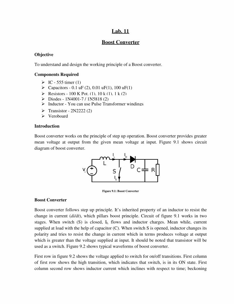
Boost converter works on the principle of step up operation. Boost converter provides greater
mean voltage at output from the given mean voltage at input. Figure 9.1 shows circuit
diagram of boost converter.
Figure 9.1: Boost Converter
Boost Converter
Boost converter follows step up principle. It’s inherited property of an inductor to resist the
change in current (di/dt), which pillars boost principle. Circuit of figure 9.1 works in two
stages. When switch (S) is closed, IL flows and inductor charges. Mean while, current
supplied at load with the help of capacitor (C). When switch S is opened, inductor changes its
polarity and tries to resist the change in current which in terms produces voltage at output
which is greater than the voltage supplied at input. It should be noted that transistor will be
used as a switch. Figure 9.2 shows typical waveforms of boost converter.
First row in figure 9.2 shows the voltage applied to switch for on/off transitions. First column
of first row shows the high transition, which indicates that switch, is in its ON state. First
column second row shows inductor current which inclines with respect to time; beckoning
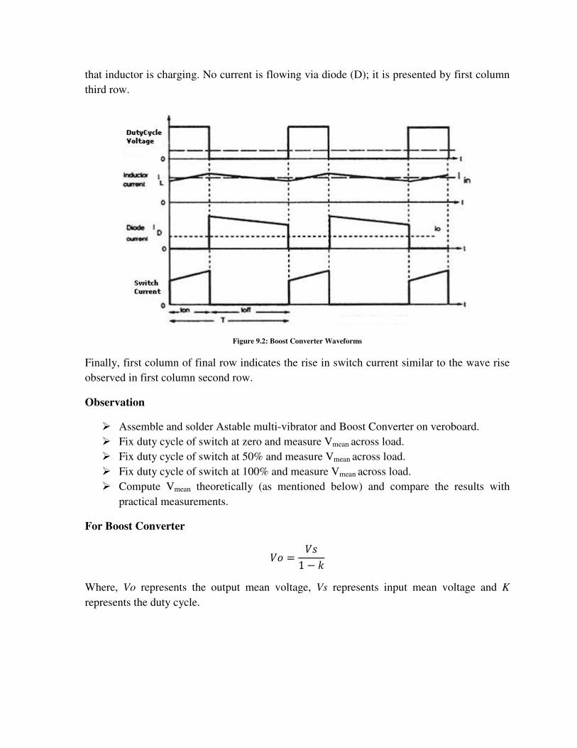
that inductor is charging. No current is flowing via diode (D); it is presented by first column
third row.
Figure 9.2: Boost Converter Waveforms
Finally, first column of final row indicates the rise in switch current similar to the wave rise
observed in first column second row.
Observation
� Assemble and solder Astable multi-vibrator and Boost Converter on veroboard.
� Fix duty cycle of switch at zero and measure Vmean across load.
� Fix duty cycle of switch at 50% and measure Vmean across load.
� Fix duty cycle of switch at 100% and measure Vmean across load.
� Compute Vmean theoretically (as mentioned below) and compare the results with
practical measurements.
For Boost Converter
�# � �$1 � &
Where, Vo represents the output mean voltage, Vs represents input mean voltage and K
represents the duty cycle.

Calculation
For Boost Converter
� Explain the second column of each row figure in fig. 9.2.
_____________________________________________________________________
_____________________________________________________________________
_____________________________________________________________________
_____________________________________________________________________
_____________________________________________________________________
_____________________________________________________________________
Task
� Simulate Buck-Boost Converter in Pspice.
Lab. 12
Buck-Boost Converter
Objective
To understand and design the working principle of a Buck-Boost converter.
Components Required
� IC - 555 timer (1) � Capacitors - 0.1 uF (2), 0.01 uF(1), 100 uF(1)
� Resistors - 100 K Pot. (1), 10 k (1), 1 k (2)
� Diodes - 1N4001-7 / 1N5818 (4)
� Inductor - You can use Pulse Transformer windings
� Transistor - 2N2222 (2)
� Veroboard
Introduction
Buck-Boost converter follows the principle of step up and step down operation. It is also
known as step up/down converter. Output mean voltages of buck-boost converter can be
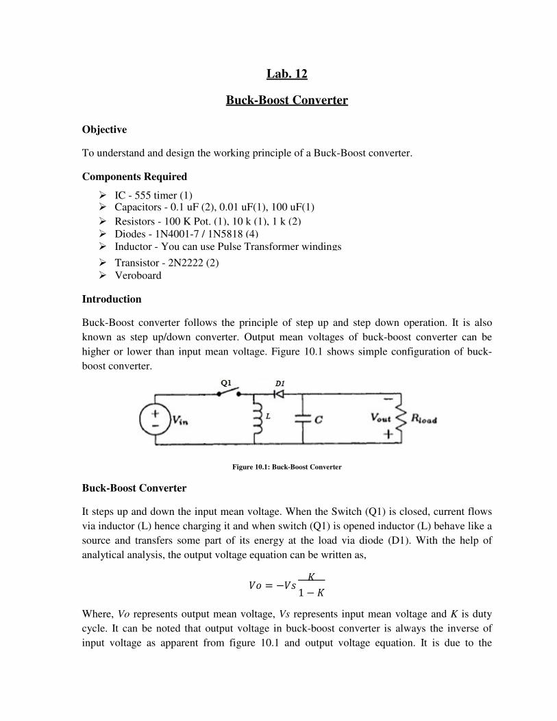
higher or lower than input mean voltage. Figure 10.1 shows simple configuration of buck-
boost converter.
Figure 10.1: Buck-Boost Converter
Buck-Boost Converter
It steps up and down the input mean voltage. When the Switch (Q1) is closed, current flows
via inductor (L) hence charging it and when switch (Q1) is opened inductor (L) behave like a
source and transfers some part of its energy at the load via diode (D1). With the help of
analytical analysis, the output voltage equation can be written as,
�# � ��$ %1 � %
Where, Vo represents output mean voltage, Vs represents input mean voltage and K is duty
cycle. It can be noted that output voltage in buck-boost converter is always the inverse of
input voltage as apparent from figure 10.1 and output voltage equation. It is due to the

charging and discharging property of inductor. A simplified way for analysing the circuit of
figure 10.1 is to assume an inductor as an energy storage element. When Q1 is ON, inductor
charges and when Q1 is OFF inductor behave like a source and releases some of its energy at
load. Hence, the more the Q1 remains ON, the more the inductor is going to release its
energy at load and converse is also true.
Observation
� Assemble and solder Astable multi-vibrator and Buck-Boost Converter on veroboard.
� Fix duty cycle of switch at zero and measure Vmean across load.
� Fix duty cycle of switch at 50% and measure Vmean across load.
� Fix duty cycle of switch at 20% and measure Vmean across load.
� Fix duty cycle of switch at 80% and measure Vmean across load.
� Compute Vmean theoretically (as mentioned below) and compare the results with
practical measurements.
For Buck-Boost Converter
�# � ��$ %1 � %
Where, Vo represents the output mean voltage, Vs represents input mean voltage and K
represents the duty cycle.
Calculation
For Buck-Boost Converter
Task
� Simulate Cừk Converter in Pspice.
Lab. 13
Cừk Converter
Objective
To understand and design the working principle of Cừk Converter.
Components Required
� IC - 555 timer (1) � Capacitors - 0.1 uF (2), 0.01 uF(1), 100 uF(1)
� Resistors - 100 K Pot. (1), 10 k (1), 1 k (2)
� Diodes - 1N4001-7 / 1N5818 (4)
� Inductor - You can use Pulse Transformer windings
� Transistor - 2N2222 (2)
� Veroboard
Introduction
As buck-boost converter, Cừk converter also follows the principle of step up and step down
of mean voltages at the output. Cừk converter produces the output mean voltage either higher
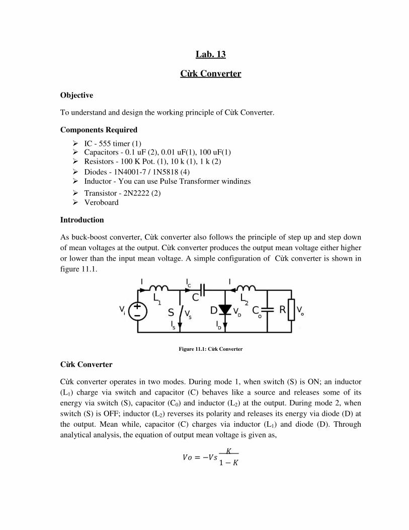
or lower than the input mean voltage. A simple configuration of Cừk converter is shown in
figure 11.1.
Figure 11.1: Cừk Converter
Cừk Converter
Cừk converter operates in two modes. During mode 1, when switch (S) is ON; an inductor
(L1) charge via switch and capacitor (C) behaves like a source and releases some of its
energy via switch (S), capacitor (C0) and inductor (L2) at the output. During mode 2, when
switch (S) is OFF; inductor (L2) reverses its polarity and releases its energy via diode (D) at
the output. Mean while, capacitor (C) charges via inductor (L1) and diode (D). Through
analytical analysis, the equation of output mean voltage is given as,
�# � ��$ %1 � %

Where, Vo represents output mean voltage, Vs represents input mean voltage and K is duty
cycle. It can be noted that output voltage in Cừk converter is always the inverse of input
voltage as apparent from output voltage equation.
Why Cừk converter when Buck-Boost converter is Available ?
So, like the buck-boost converter, the Cừk converter can step the voltage either up or down,
depending on the switching duty cycle. The main difference between the two is that because
of the series inductors at both input and output, the Cừk converter has much lower current
ripple. In fact by careful adjustment of the inductor values, the ripple in either input or output
can be nulled completely.
Observation
� Assemble and solder Astable multi-vibrator and Cừk Converter on veroboard.
� Fix duty cycle of switch at zero and measure Vmean across load.
� Fix duty cycle of switch at 50% and measure Vmean across load.
� Fix duty cycle of switch at 20% and measure Vmean across load.
� Fix duty cycle of switch at 80% and measure Vmean across load.
� Compute Vmean theoretically (as mentioned below) and compare the results with
practical measurements.
For Cừk Converter
�# � ��$ %1 � %
Where, Vo represents the output mean voltage, Vs represents input mean voltage and K
represents the duty cycle.
Calculation
For Cừk Converter
Task
� Simulate Single Phase Full Bridge Inverter in Pspice.
Objective
To understand and design the working principle of a Single Phase Full Bridge Inverter.
Components Required
� IC - 555 timer (1)
� Capacitors - 0.1 uF (2), 0.01 uF(1), 100 uF(1)
� Resistors - 100 K Pot. (1), 10 k (1), 1 k (2)
� Diodes - 1N4001-7 / 1N5818 (4
� Transistor - 2N2222 (10
� Pulse Transformer – Solo Winding (4)
� Veroboard
Introduction
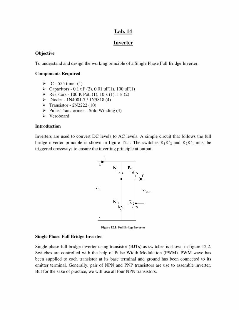
Inverters are used to convert DC levels to AC levels. A simple circuit that follows the full
bridge inverter principle is shown in figure 12.1. The switches K
triggered crossways to ensure the inverting principle at output.
Single Phase Full Bridge Inverter
Single phase full bridge inverter using transistor (BJTs) as switches is shown in figure 12.2.
Switches are controlled with the help of Pulse Width Modulation (PWM). PWM wave has
been supplied to each transistor at its base terminal and ground has been connected to its
emitter terminal. Generally, pair of NPN and PNP transistors are use to assemble inverter.
But for the sake of practice, we will use all four NPN transistors.
Lab. 14
Inverter
design the working principle of a Single Phase Full Bridge Inverter.
0.1 uF (2), 0.01 uF(1), 100 uF(1)
100 K Pot. (1), 10 k (1), 1 k (2)
/ 1N5818 (4)
(10)
Solo Winding (4)
Inverters are used to convert DC levels to AC levels. A simple circuit that follows the full
bridge inverter principle is shown in figure 12.1. The switches K1K’2 and K
triggered crossways to ensure the inverting principle at output.
Figure 12.1: Full Bridge Inverter
Single Phase Full Bridge Inverter
Single phase full bridge inverter using transistor (BJTs) as switches is shown in figure 12.2.
rolled with the help of Pulse Width Modulation (PWM). PWM wave has
been supplied to each transistor at its base terminal and ground has been connected to its
emitter terminal. Generally, pair of NPN and PNP transistors are use to assemble inverter.
the sake of practice, we will use all four NPN transistors.
design the working principle of a Single Phase Full Bridge Inverter.
Inverters are used to convert DC levels to AC levels. A simple circuit that follows the full
and K2K’1 must be
Single phase full bridge inverter using transistor (BJTs) as switches is shown in figure 12.2.
rolled with the help of Pulse Width Modulation (PWM). PWM wave has
been supplied to each transistor at its base terminal and ground has been connected to its
emitter terminal. Generally, pair of NPN and PNP transistors are use to assemble inverter.
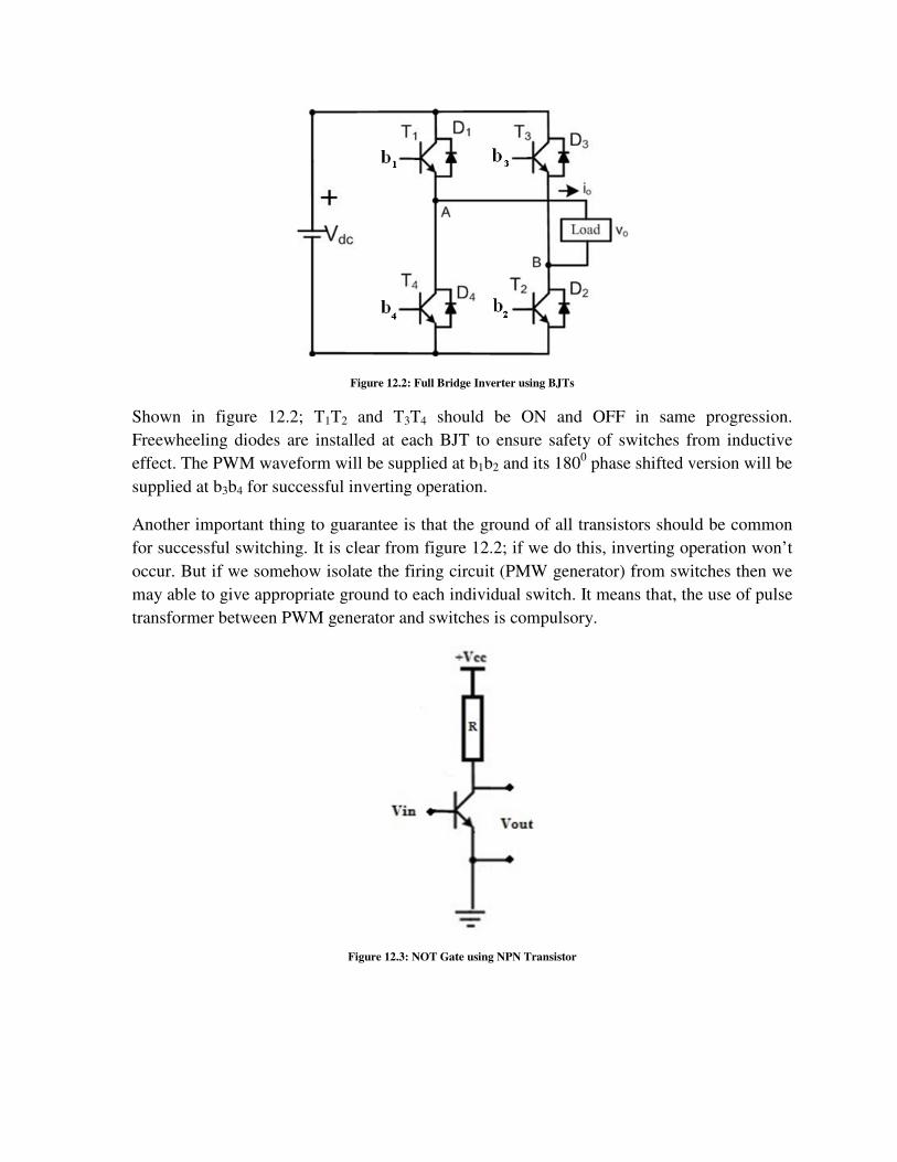
Figure 12.2: Full Bridge Inverter using BJTs
Shown in figure 12.2; T1T2 and T3T4 should be ON and OFF in same progression.
Freewheeling diodes are installed at each BJT to ensure safety of switches from inductive
effect. The PWM waveform will be supplied at b1b2 and its 1800 phase shifted version will be
supplied at b3b4 for successful inverting operation.
Another important thing to guarantee is that the ground of all transistors should be common
for successful switching. It is clear from figure 12.2; if we do this, inverting operation won’t
occur. But if we somehow isolate the firing circuit (PMW generator) from switches then we
may able to give appropriate ground to each individual switch. It means that, the use of pulse
transformer between PWM generator and switches is compulsory.
Figure 12.3: NOT Gate using NPN Transistor

1800 Phase Shift using an NPN Transistor
1800 phase shift can be introduced by making a simple NOT gate using an NPN transistor.
Figure 12.3 shows a simple NOT gate. If a signal having voltage X is given at the base of
transistor, the output acquired voltage will be X’ and it will be 1800 phase shifted version of
the input signal. In above figure ‘R’ represents resistance.
Observation
� Assemble and solder Astable multi-vibrator and single phase full bridge Inverter on
veroboard.
� Examine the nature of output voltage and variations when you alter the input mean
voltage.
For Single Phase Full Bridge Inverter
�'()& � �*+
Where, Vpeak represents the output peak of AC voltage and Vin represents input mean
voltage.
Waveforms
For Phase Full Bridge Inverter Input with specified Mean Value:
For Phase Full Bridge Inverter Output with specified Peak Value: