power management circuits for energy harvesting
TRANSCRIPT

POWER MANAGEMENT CIRCUITS FOR ENERGY HARVESTING
APPLICATIONS
A Dissertation
by
SALVADOR CARREON-BAUTISTA
Submitted to the Office of Graduate and Professional Studies of
Texas A&M University
in partial fulfillment of the requirements for the degree of
DOCTOR OF PHILOSOPHY
Chair of Committee, Edgar Sánchez-Sinencio
Committee Members, Kamran Entesari
Arum Han
Kenith Meissner
Head of Department, Miroslav M. Begovic
May 2015
Major Subject: Electrical Engineering
Copyright 2015 Salvador Carreon-Bautista

ii
ABSTRACT
Energy harvesting is the process of converting ambient available energy into
usable electrical energy. Multiple types of sources are can be used to harness
environmental energy: solar cells, kinetic transducers, thermal energy, and
electromagnetic waves.
This dissertation proposal focuses on the design of high efficiency, ultra-low
power, power management units for DC energy harvesting sources. New architectures
and design techniques are introduced to achieve high efficiency and performance while
achieving maximum power extraction from the sources. The first part of the dissertation
focuses on the application of inductive switching regulators and their use in energy
harvesting applications. The second implements capacitive switching regulators to
minimize the use of external components and present a minimal footprint solution for
energy harvesting power management. Analysis and theoretical background for all
switching regulators and linear regulators are described in detail.
Both solutions demonstrate how low power, high efficiency design allows for a
self-sustaining, operational device which can tackle the two main concerns for energy
harvesting: maximum power extraction and voltage regulation. Furthermore, a practical
demonstration with an Internet of Things type node is tested and positive results shown
by a fully powered device from harvested energy. All systems were designed,
implemented and tested to demonstrate proof-of-concept prototypes.

iii
DEDICATION
Para mis padres Salvador y Marisa, cuyo apoyo y ejemplo me han fortalecido
cuando lo necesitaba.
Para mi esposa Pilar, que estuvo conmigo todo el camino sin yo darme cuenta.

iv
ACKNOWLEDGEMENTS
I am enormously grateful for the people that have helped me accomplish what is
presented in this dissertation. I thank my advisor, Dr. Edgar Sanchez-Sinencio, for his
knowledge, advice, and friendship throughout my studies here at Texas A&M. If it not
for his invitation to visit College Station, I would not be writing this today.
I would like to thank my committee members, Dr. Kamran Entesari, Dr. Arum
Han, and Dr. Kenith Meissner, for their guidance and support throughout the course of
this research. I would like to thank Professors Ahmed Emira Eladawy and Ahmed
Mohieldin for their help and insight for our projects.
Thanks also go to my friends and colleagues and the department faculty and staff
for making my time at Texas A&M University a great experience. Special thanks to the
friends I had the privilege of meeting and working alongside. I would like to greatly
thank Joselyn Torres and Jorge Zarate, for being both great friends and mentors
throughout my time at the AMSC. I would also like to thank Efrain Gaxiola, Miguel
Rojas, Xiaosen Liu, Roland Ribeiro, Judy Amanor-Boadu, Jiayi Jin, Carlos Briseño,
Fernando Lavalle, Alfredo Costilla, Congyin Shi, Mohamed Abouzied, Felix Fernandez,
Roland Ribeiro, as well as Celal Erbay for putting up with my incessant emails and texts
asking if we could perform tests on the fuel cells.
I would also like to thank Ms. Ella Gallagher for her help and humor throughout
my time at the AMSC.

v
Furthermore, I would like to extend my thanks to the National Council on
Science and Technology of Mexico for the economic support during my doctoral studies.
Finally, I am forever thankful for my mother and father, for their encouragement
and support; my brother and sister for their own perspective and outlook on things; and
to my wife Pilar for her patience, love, and understanding.

vi
TABLE OF CONTENTS
Page
ABSTRACT .......................................................................................................................ii
DEDICATION ................................................................................................................. iii
ACKNOWLEDGEMENTS .............................................................................................. iv
TABLE OF CONTENTS .................................................................................................. vi
LIST OF FIGURES ............................................................................................................ x
LIST OF TABLES ....................................................................................................... xviii
CHAPTER I INTRODUCTION ....................................................................................... 1
Energy harvesting ....................................................................................... 1 Applications and need for power management .......................................... 2 Energy harvesting sources .......................................................................... 6
Thermoelectric generators .............................................................. 6 Photovoltaic cells ......................................................................... 13 Radiofrequency harvesting ........................................................... 18
Kinetic energy harvesting ............................................................. 24 Alternative energy harvesting sources ......................................... 29
Voltage regulators .................................................................................... 33 Inductive switching regulators ..................................................... 33 Capacitive switching regulators ................................................... 36 Linear regulators .......................................................................... 38
Energy storage elements ........................................................................... 40 Power management’s significance on energy harvesting technology ...... 41 Proposed solution ..................................................................................... 42
CHAPTER II FUNDAMENTALS OF POWER MANAGEMENT SYSTEMS FOR
ENERGY HARVESTING ............................................................................................... 47
Introduction .............................................................................................. 47 Switching converter fundamentals ........................................................... 50
Step-up (boost converter) ............................................................. 50 Operating modes .......................................................................... 55 Boost converter control Loop for Pulse Width Modulation ......... 63 Boost converter Control Loop for Pulse Frequency
Modulation ................................................................................... 64

vii
Step-up (switched capacitor) ........................................................ 67 Switched capacitor control loop for pulse width
modulation .................................................................................... 73 Switched capacitor control loop for pulse frequency
modulation .................................................................................... 75 Performance comparison .......................................................................... 77
Voltage gain ratio ......................................................................... 77 Power efficiency ........................................................................... 78 Integration .................................................................................... 81
Trade-offs ..................................................................................... 82 Linear regulators ...................................................................................... 84
Low dropout regulators ................................................................ 84
Principles ...................................................................................... 86 Digital LDO approach .................................................................. 89 Performance comparison and state-of-the-art .............................. 93
CHAPTER III A BOOST CONVERTER WITH DYNAMIC INPUT IMPEDANCE
MATCHING FOR DC ENERGY HARVESTING SOURCES ...................................... 95
Introduction .............................................................................................. 95 Maximum power point tracking ............................................................... 98 Proposed dynamic matching for boost converter ................................... 100
Block diagram for dynamic MPPT ............................................ 102 Algorithm for pseudo zero current switching ............................ 110
Output voltage setting ................................................................ 111
Building block circuit implementation ................................................... 112
Divider (extraction of Voc/2) ...................................................... 112 Comparators (KP) and charge pump (KCP) ................................. 113
Voltage controlled oscillator ...................................................... 114 Filter ........................................................................................... 114 Pseudo zero current switching .................................................... 115
Startup ........................................................................................ 117 Experimental results ............................................................................... 118
MPPT impedance tracking ......................................................... 119 P-ZCS waveforms ...................................................................... 120
Efficiency measurements ........................................................... 121 Conclusions ............................................................................................ 122
CHAPTER IV POWER MANAGEMENT SYSTEM WITH INTEGRATED
MAXIMUM POWER EXTRACTION ALGORITHM FOR MICROBIAL FUEL
CELLS ............................................................................................................................ 124
Introduction ............................................................................................ 124 MFC and power management system specifications ............................. 126

viii
MFC construction and characterization ..................................... 127 MFC electrical equivalent modeling .......................................... 129 System specifications ................................................................. 130
Adaptable maximum power extraction algorithm .................................. 131 Current state-of-the-art ............................................................... 131 Overview of the proposed MPEA system .................................. 133 Operating point for impedance tracking ..................................... 134 MPEA and ZCST loops .............................................................. 136
Circuit implementation for PMS ............................................................ 138 Operating point for impedance tracking implementation .......... 140 MPEA implementation ............................................................... 147 Zero current switching tracking loop ......................................... 148
Output voltage setting ................................................................ 150 Power management system startup ............................................ 152
Experimental results and discussion ...................................................... 152 Maximum power extraction algorithm ....................................... 153 Zero current switching tracking ................................................. 154 Total power consumption and efficiency ................................... 155 Discussion .................................................................................. 158
Conclusions ............................................................................................ 160
CHAPTER V AN INDUCTORLESS DC-DC CONVERTER FOR AN ENERGY
AWARE POWER MANAGEMENT UNIT FOR MICROBIAL FUEL CELLS ......... 161
Introduction ............................................................................................ 161
MFC array and power extraction methodology ..................................... 163 State-of-the-art ........................................................................... 164 MFC construction and operation ................................................ 165 MFC electrical equivalent circuit ............................................... 167 Inductorless DC-DC converter ................................................... 168
Maximum power extraction for MFC array ........................................... 170 Input resistance for I-DC DC ..................................................... 171 I-DCDC stability with reconnection .......................................... 175
I-DCDC implemented circuit blocks ...................................................... 179 Maximum power point and comparator blocks .......................... 179
Charge pump and filter ............................................................... 181 Current controlled oscillator ....................................................... 182
10X step-up charge pump .......................................................... 182 I-DCDC system startup .............................................................. 186
Measurement results ............................................................................... 186 Maximum power point tracking ................................................. 188 Voltage regulation ...................................................................... 189
Efficiency measurement ............................................................. 190 Conclusions ............................................................................................ 193

ix
CHAPTER VI AN AUTONOMOUS FULLY INTEGRATED ENERGY
HARVESTING POWER MANAGEMENT UNIT WITH DIGITAL REGULATION
FOR IOT APPLICATIONS ........................................................................................... 194
Introduction ............................................................................................ 194
Proposed power management unit ......................................................... 196 Startup block .............................................................................. 197 Main converter charge pump ...................................................... 198 Low power digital LDO ............................................................. 200
Circuit block implementation ................................................................. 202
Startup block .............................................................................. 202 Digital maximum power point tracking ..................................... 204
Main converter charge pump ...................................................... 211 Digital low dropout regulator ..................................................... 213
Measurement results ............................................................................... 217 Startup scheme ........................................................................... 218
Digital maximum power point tracking ..................................... 219 Voltage regulation (digital LDO) ............................................... 221
Wireless sensor node temperature sensor testing ....................... 221 Power consumption and efficiency ............................................ 223
Conclusions ............................................................................................ 226
CHAPTER VIII SUMMARY AND FUTURE WORK ................................................ 227
REFERENCES ............................................................................................................... 229
APPENDIX .................................................................................................................... 249

x
LIST OF FIGURES
Page
Fig. 1. Power density comparison of battery density improvement over time vs.
processing power density improvement over time. ................................................ 1
Fig. 2. Overview of wireless sensor node with power management unit highlighted. ...... 5
Fig. 3. Seebeck effect principle between two different metals. ......................................... 7
Fig. 4. Peltier effect principle through applied voltage source. ......................................... 8
Fig. 5. Thomson effect showing absorption or dissipation by a single type of material
with both temperature difference and current passed through it. ........................... 9
Fig. 6. Basic TEG building block consisting of n- and p-type
semiconductor elements. ...................................................................................... 10
Fig. 7. Figure of merit (ZT) for current TEG materials [22]. ........................................... 12
Fig. 8. TEG module’s electrical equivalent. ..................................................................... 12
Fig. 9. Band diagram of p-n junction showing diffusion directions and electron drift. ... 14
Fig. 10. Equivalent circuit of photovoltaic cell. ............................................................... 15
Fig. 11. RF energy harvesting system. ............................................................................. 19
Fig. 12. AC-DC rectifier. ................................................................................................. 21
Fig. 13. Positive and negative half-cycle performance for RF AC-DC rectifier. ............ 21
Fig. 14. N-stage AC-DC rectifier block for RF energy harvesting. ................................. 22
Fig. 15. Diode and NMOS implementation of AC-DC rectifier block for RF
harvesting. ........................................................................................................... 23
Fig. 16. Schematic of three types of electromechanical transducers a) electrostatic
b) electromagnetic and c) piezoelectric, from [37]. ............................................ 24
Fig. 17. Piezoelectric effect showing ceramic cation and anion reconfiguration
with both external polarization voltage and deformation forces applied. ........... 25
Fig. 18. Piezoelectric energy harvester electrical model. ................................................. 28

xi
Fig. 19. Microbial fuel cell two-chamber schematic. ....................................................... 30
Fig. 20. Output voltage of MFC vs. time. ........................................................................ 31
Fig. 21. Microbial fuel cell simplified electrical equivalent model. ................................ 32
Fig. 22. A) Switching phases and B) inductor current waveform of an inductive
switching regulator. ............................................................................................ 34
Fig. 23. Operation and switching waveforms for a simple voltage doubler. ................... 36
Fig. 24. Linear regulator simplified schematic................................................................. 38
Fig. 25. Conceptual comparison of power density vs. energy density in batteries and
super/ultra-capacitors. ......................................................................................... 41
Fig. 26. Proposed solution for TEG array impedance matching and
energy harvesting. ............................................................................................... 43
Fig. 27. Proposed solution for MFC source impedance matching and energy
harvesting. ........................................................................................................... 44
Fig. 28. Proposed solution for MFC array impedance matching and
energy harvesting. ............................................................................................... 45
Fig. 29. Proposed solution for DC energy harvesting autonomous power
management unit. ................................................................................................ 46
Fig. 30. Switching converter power conversion illustration. ........................................... 47
Fig. 31. Illustrative example of linear regulator. .............................................................. 49
Fig. 32. Boost converter schematic. ................................................................................. 50
Fig. 33. Boost converter complementary phase operation. .............................................. 51
Fig. 34. A) Asynchronous boost converter schematic and B) synchronous boost
converter schematic. ........................................................................................... 52
Fig. 35. Boost converter CCM and DCM inductor current waveforms. .......................... 53
Fig. 36. DC and small signal models for CCM and DCM PWM switch
implementations. ................................................................................................. 54
Fig. 37.DCM operating mode view of switch activation and behavior during
each cycle. ........................................................................................................... 54

xii
Fig. 38. Boost power stage with connection structure for PWM model. ......................... 56
Fig. 39. AC small-signal averaged switch network model in DCM. ............................... 61
Fig. 40. Complete control loop for switching converter regulator with two different
modulation implementation options: PWM and PFM. ....................................... 63
Fig. 41. Implementation of PWM scheme. ...................................................................... 64
Fig. 42. Implementation of PFM scheme. ........................................................................ 65
Fig. 43. AC small-signal averaged switch network model in DCM un PFM. ................. 66
Fig. 44. Dynamic behavior of charge pump. .................................................................... 69
Fig. 45. Diode, MOSFET, and bootstrap switch schemes for charge pump
implementations. ................................................................................................. 70
Fig. 46. Single stage switched capacitor converter with associated
capacitor voltages. .............................................................................................. 71
Fig. 47. Charge pump PWM implementation. ................................................................. 74
Fig. 48. PFM behavioral model for step-up operation. .................................................... 75
Fig. 49. Output resistance with variable switching frequency and number of stages. ..... 76
Fig. 50. Voltage conversion ratio for both regulators under light-load conditions. ......... 78
Fig. 51. Power efficiency for boost converter with variable duty cycle
and increasing output load current in DCM........................................................ 79
Fig. 52. Power efficiency for charge pump with variable load current
and increasing number of stages. ........................................................................ 80
Fig. 53. Parasitic capacitance for on-chip capacitors implemented for charge
pumps. ................................................................................................................. 81
Fig. 54. Input-output voltage characteristic of Linear regulator. ..................................... 83
Fig. 55. Common-collector LDO topology with NPN active device. .............................. 85
Fig. 56. Common-source LDO topology with NMOS active device. .............................. 86
Fig. 57. Small-signal pole locations for source-follower topology. ................................. 88

xiii
Fig. 58. Small-signal pole locations for common-source topology. ................................ 89
Fig. 59. Digital LDO implementation with PMOS array for pass devices. ..................... 91
Fig. 60. Voltage domain controller for digital LDO implementation. ............................. 92
Fig. 61. Multi-array TEG grid parallel (top), series (bottom) configuration. .................. 96
Fig. 62. Schematic of BC with synchronous rectification. ............................................... 98
Fig. 63. Contour plots of input resistance variation with Lin and fs. ............................... 101
Fig. 64. Block diagram of proposed MPPT system. ...................................................... 103
Fig. 65. Block diagram for MPPT implementation. ....................................................... 104
Fig. 66. Small-signal linear model of MPPT block. ....................................................... 105
Fig. 67. Control-to-input voltage transfer function model of boost converter. .............. 106
Fig. 68. Analytical (5) vs. simulated results: (left) magnitude, (right) phase. ............... 108
Fig. 69. Inductor current behavior for P-ZCS scheme. .................................................. 109
Fig. 70. Pseudo-ZCS control algorithm. ........................................................................ 110
Fig. 71. Divider circuit implemented [91] ...................................................................... 113
Fig. 72. Implementation of delay array for PMOS on/off time. ..................................... 117
Fig. 73. Die microphotograph ........................................................................................ 118
Fig. 74. Input voltage regulation maintaining MPPT under large variations of RTEG
(VOC=200 mV). ................................................................................................. 119
Fig. 75. P-ZCS scheme implementing variable DPMOS duty cycles to minimize
inductor losses................................................................................................... 120
Fig. 76. Measured efficiency for system under varying RTEG values for
RTEG =[33.33Ω to 300Ω] Iload≈14μA,for RTEG =[600Ω to 2.7kΩ] Iload =1μA. .. 121
Fig. 77. Schematic of conventional two-chamber MFC. ............................................... 126
Fig. 78. The 240 mL two-chamber MFC constructed and used for the PMS
characterization, connections follow Fig. 77. ................................................... 127
Fig. 79. Power-resistance and voltage-resistance characteristics of the MFC. .............. 128
xiv
Fig. 80. A) Stead-state electrical mode (Vdc) and B) dynamic model (Vs) of the
MFC. ................................................................................................................. 129
Fig. 81. Conceptual representation of the proposed power management system. ......... 133
Fig. 82. Obtaining MPP voltage (Vcomp) from the MFC through MPEA. ...................... 135
Fig. 83. Overview of the proposed PMS with the MPEA section highlighted. ............. 137
Fig. 84. Fundamental schematic of the boost converter used here as part of the
PMS circuit. ...................................................................................................... 138
Fig. 85. (Left) Measured RC time constant (τMFC) of the MFC device and (right)
illustration of time needed to charge the capacitor C1 to read the
open circuit voltage VMFC. ................................................................................. 140
Fig. 86. Relationship between ϕ2 and ϕ1. ....................................................................... 141
Fig. 87. Operating point tracking for dynamic range, phase ϕ2 sampling of VMFC
and phase ϕ2 dividing VMFC by two. ................................................................. 143
Fig. 88. Dynamic range showing correct MPP. ............................................................. 144
Fig. 89. Operating point tracking for manual range, (ϕ2) sampling of Vout and (ϕ1)
dividing Vcomp by two. ...................................................................................... 145
Fig. 90. Manual range showing correct MPP. ................................................................ 146
Fig. 91. Impedance tracking scheme for MPEA. ........................................................... 147
Fig. 92. Inductor current and ZCST parameters. ............................................................ 149
Fig. 93. Zero current switching tracking loop for Tp time control. ................................ 149
Fig. 94. VP generation for TP signal. .............................................................................. 150
Fig. 95. Internal voltage supply for controller and driver acquisition fromVout. ............ 151
Fig. 96. Overall testing setup to characterize the PMS controlling the MFC. ............... 152
Fig. 97. Die microphotograph. ....................................................................................... 153
Fig. 98. Input and output voltage profiles at steady state with ~75μA load. ................. 154
Fig. 99. ZCST loop minimizing losses from inductor current switching. ...................... 155

xv
Fig. 100. Overall PMS power consumption breakdown. ............................................... 156
Fig. 101. Measured efficiency vs. delivered power. ...................................................... 158
Fig. 102. Possible implementation with presented PMS for battery extending
operation. ......................................................................................................... 159
Fig. 103. a) Schematic of a two chamber microbial fuel cell. b) The small
(MFC-L) and large (MFC-H) devices used with I-DCDC. ............................. 165
Fig. 104. Simplified electrical equivalent circuit for an MFC device. ........................... 167
Fig. 105. Proposed structure of the energy aware-power management unit. ................. 169
Fig. 106. Input resistance variation for inductorless DC-DC converter. ........................ 173
Fig. 107. Small-signal equivalent MFC source impedance for control-to-input
transfer function. ............................................................................................. 174
Fig. 108. Control-to-input simulated and analytical comparison. .................................. 176
Fig. 109. Small-signal stability model for PMU MPPT scheme. ................................... 177
Fig. 110. Implemented MPPT scheme through frequency modulation scheme. ........... 178
Fig. 111. Capacitive divider for MPP acquisition from output voltage (left)
and directly from input voltage (right). ........................................................... 180
Fig. 112. 10X charge pump topology. ............................................................................ 183
Fig. 113. Bootstrap technique for CP stage. ................................................................... 184
Fig. 114. Stage control block for output voltage monitoring. ........................................ 185
Fig. 115. Die microphotograph of implemented I-DCDC and test bench. .................... 186
Fig. 116. Power production of MFC-L (low power) and MFC-H (high power). ........... 187
Fig. 117. The MPPT control loop correctly identifying MPP for
extreme condition MFC-H and MFC-L. ......................................................... 188
Fig. 118. Output voltage load regulation test with load current variation for
1.6 mW of input power. .................................................................................. 189
Fig. 119. Efficiency measurements for CP with variable loads. .................................... 190

xvi
Fig. 120. Power consumption for I-DCDC @ 1 MHz fsw (left) and
10 kHz fsw (right). ............................................................................................ 191
Fig. 121. Proposed block diagram of the power management unit. ............................... 196
Fig. 122. Startup scheme generating a supply rail for the main converter to begin
operation. ......................................................................................................... 198
Fig. 123. Digital maximum power point tracking with maximum power point
acquisition block for main converter. .............................................................. 199
Fig. 124. Main converter (10x) showing bypassing capabilities through stage
control block. ................................................................................................... 200
Fig. 125. Digital LDO regulation scheme. ..................................................................... 202
Fig. 126. Startup scheme clock generation and enable timer block. .............................. 203
Fig. 127. Maximum power point acquisition scheme for difference dc EH sources a)
thermoelectric generators, b) PV solar cells, c) Microbial fuel cells
(MFCs), and d) the timing diagrams for both switching phases. .................... 205
Fig. 128. Digital controlled oscillator implementation for DMPPT. ............................. 208
Fig. 129. Digitally controlled oscillator frequency range and code word in
hexadecimal format. ........................................................................................ 209
Fig. 130. Input resistance range capabilities for proposed PMU with a) varying
charge pumps stages v. fsw and b) varying output voltages v. fsw. ................... 210
Fig. 131. Full schematic of 10X main converter with variable stage selection. ............ 210
Fig. 132. Stage control block with low power reference schematic. ............................. 212
Fig. 133. LDO pass device array selector. ..................................................................... 214
Fig. 134. Digital LDO implementation. ......................................................................... 215
Fig. 135. a) Die microphotograph and b) PCB footprint comparison to
US quarter. ...................................................................................................... 218
Fig. 136. Startup scheme with handoff operation to main converter. ............................ 218
Fig. 137. Digital maximum power point tracking efficiency for MFC, TEG,
and PV solar cells. ........................................................................................... 220

xvii
Fig. 138. Digital low-dropout regulator load regulation test for 1.75 mW
of input power and a 900 μA step load current. .............................................. 220
Fig. 139. Internet of Things (IoT) testing configuration A) illustration of power
management unit with temperature sensor and B) unfolded
implementation for IoT configuration with thermoelectric generator unit. .... 221
Fig. 140. Wireless sensor node testing voltage profile A) with 1F supercapacitor
at Cstore and B) temperature sensor transmitted results. ................................... 222
Fig. 141. Power consumption by block for PMU at a) 500 kHz fsw
and b) 5 MHz fsw. ............................................................................................. 223
Fig. 142. End-to-end efficiency for 9 stage enabled (10X gain) main converter
and digital LDO. .............................................................................................. 224
Fig. 143. 9 stage I-DCDC converter with associated capacitor voltages. ...................... 249
Fig. 144. Open loop gain and phase margin with optimized filter design. .................... 251
Fig. 145. Effect of stability in MPPT when switching between MFCs
(MFC-H to MFC-L) and unstable response. ................................................... 252

xviii
LIST OF TABLES
Page
Table 1. Energy harvesting estimates in μW per unit of area [16]. ................. ................. 3
Table 2. Solar efficiency tables for multiple photovoltaic cell materials ......................... 17
Table 3. Small-signal DCM switch model parameters ..................................................... 61
Table 4. Small-signal model parameters for boost converter in DCM
under PFM. ..................................................................................................... 66
Table 5. Comparison table for both regulator topologies presented. ............................... 83
Table 6. Comparison table with state-of-the-art digital LDO implementations. ............. 94
Table 7. Design specification for converter. .................................................................. 100
Table 8. Performance summary ...................................................................................... 123
Table 9. MFC PMS system specifications. .................................................................... 131
Table 10. Comparison of MFC power management units. ............................................ 157
Table 11. Microbial fuel cell parameters ........................................................................ 168
Table 12. Summary of performance for MFC power management units. ...................... 192
Table 13. Power detection logic parameters for LDO array selector. ............................ 216
Table 14. Performance summary .................................................................................... 225

1
CHAPTER I
INTRODUCTION
Energy harvesting
As power demands continue to grow for integrated solutions, new ways to extend
device lifetime must be developed to maintain high energy dense solutions plausible.
And even though battery technology has shown unprecedented growth and application
[1, 2], compact solutions with limited area real-estate still show lagging power when
compared to transistor power density [3]. Fig. 1 shows a comparison between battery
power density improvements over the course of 20 years compared to the processing
power of integrated solution over the same time frame.
Fig. 1. Power density comparison of battery density improvement over time vs. processing power
density improvement over time.
Time (yr.)
1 10 20
Scalin
g (
x)
103
102
101
10
1
Transistor Density
Battery Power Density
4X increase
over 20 years

2
As the figure shows, battery technology deeply lags behind processing power,
and there is only a 2X improvement shown every 10 years [4].
This leads to a very real need to enhance battery life for small, portable
applications in order to allow wireless sensor technologies a real shot of being
implemented. Among the possible solutions to enhance operational lifetime, or even
disregard the need for battery technology all-together, of wireless sensors is energy
harvesting. Energy harvesting is the process of scavenging energy that is readily and
freely available in the environment, into electrical energy [5, 6]. Similar to large scale
energy farms seen with photovoltaic solar cells, energy harvesting targets the available
energy in one form to convert to electrical and utilize it to power small devices/systems.
The only difference lies in the scale of the targeted power to be harvested.
Whereas macro-harvesting systems are related to energy conversion in the range of
kilowatts to Megawatts, energy harvesting is limited to harvesting power in the range of
nanowatts to milliwatts. Even at these low power levels, much can be accomplished
through smart, low-power electronic design through the implementation of
environmental sensors [7], healthcare monitoring nodes [8], and data networking for
large-scale operations [9].
Applications and need for power management
Applications such as Wireless sensor nodes (WSN) or Internet of Things (IoT)
[10-12] arrangements allows for a distributed approach to power consumption duties.
Whereas several nodes in a mesh configuration may perform the sensing operation of the

3
network, only a select few of nodes within the mesh hold the responsibility of
transmitting the power over long distances to the central processing unit [12]. These
types of approaches focus more on delegating responsibilities and lightening the load on
a single node, redistributing it throughout the network. Alternate approaches focus on
dealing with power limited designs through intelligent package transmission [13-15].
These methods limit packet size transmission to minimize the use of the system power
amplifier (PA), which is the most power hungry and inefficient block in transmitter
circuits. Efforts on efficiently utilizing power resources can be extended further by
employing energy harvesting technology. Utilizing energy harvesting technology is not
without its own caveats: the possible power to be harvested is limited to both amount
and availability. TABLE 1 shows the power densities per area/volume for commonly
used energy harvesting sources.
TABLE 1. Energy harvesting estimates in μW per unit of area [16].
ENERGY SOURCE HARVESTED POWER
Kinetic Vibration
Human 10s of μWs/cm2
Industrial setting 100s of μWs/cm2
Temperature Gradient
Human 10s of μWs/cm2
Industrial setting 10s of mWs/cm2
Light
Human 10s of μWs/cm2
Industrial setting 10s of mWs/cm2
Radiofrequency
GSM 100s of nWs/cm2
AM 10s of pWs/cm2
Wi-Fi 1000s of pWs/cm2
Biomass (MFCs)
240 mL (air) 600 μW

4
All available power densities from EH sources in TABLE 1, go from 10s of mWs
and below. These power densities would be available for sensor applications if the
implemented systems in charge of the power conversion were 100% efficient, which is
never the case. The power converter’s own energy consumption and losses are the main
limitations in delivering all of the available power to the load. Current research efforts
are being done on both ends, improved EH transducers and high efficiency power
converters.
Due to both the limitation and variability of the power sources in energy
harvesting, a power management units (PMU) are required to store and utilize the
harvested energy in the best way possible. As shown in Fig. 2, the PMU extracts power
from the EH source and delivers an adequate voltage level to the subsequent blocks in
the wireless sensor node.

5
Fig. 2. Overview of wireless sensor node with power management unit highlighted.
The two main blocks which make up the PMU are shown: the Energy Shaping
block and the Power Conversion block. The Energy Shaping block is in charge of
extracting maximum power from the source in order to enhance efficiency and avoid any
additional strain on the PMU when harvesting from low power scenarios. The Power
Conversion’s duties are to take the maximum available power and efficiently convert it
to the required voltage rating required by the system. This can be performed through up-
conversion [17], rectification [18], down-conversion [19] or a combination of several of
the aforementioned techniques [20]. Fig. 2 highlights the operation of both blocks with
the colored lines. Red shows the maximum power transfer operation from the Energy
Shaping block allowing maximum energy to be extracted from the source. Green and
EH Source
Power
Conversion
Energy
Shaping
ICharge
Battery
Vbatt
VCO
Power Converter
DSP
TX/RX
Max Power
Po
we
r
Load currentA
Vo
lta
ge
Time
Maximum Power
transfer
Power Management Unit
Csupercapacitor
IChargeEnergy Storage

6
Blue show the input and output voltages of the Power Conversion block. An up-
conversion operation takes place increasing the available voltage at the input to
workable voltage levels for the later sensor nodes (VCO, DSP and TX/RX blocks), as
well as delivering charging current to the battery on board.
The remainder of the chapter will focus on the principle of operation of the EH
sources, as well as the available power converter blocks found in literature and
application.
Energy harvesting sources
Harvesting energy from multiple different natural phenomena, be it thermal,
solar, kinetic, or electromagnetic waves; require specialized transducers capable of
harnessing and converting one type of energy to another. This section will delve into the
fundamental operation of the currently available transducers which are used in EH
applications.
Thermoelectric generators
Heat loss is a common occurrence in mostly all mechanical and electrical
systems used worldwide. Be it from vehicle waste heat to geothermal underground
sources, it is one of the most prevalent sources of potential untapped power today.
Thermoelectric generators focus on converting temperature gradients into electrical
energy through three different thermoelectric effects: the Seebeck effect, the Peltier
effect, and the Thomson Effect. Each one of these effects takes advantage of the
surrounding natural temperature gradient through materials special properties.

7
Fig. 3. Seebeck effect principle between two different metals.
The Seebeck effect is described as the phenomena which occur when two
dissimilar metals or semiconductors are joined together and a temperate difference
across their junctions is applied.
Fig. 3 shows the Seebeck effect principle and the generated voltage (𝑉𝑙𝑜𝑎𝑑) from
the temperature difference across the junctions of Metal A and Metal B. This leads to a
voltage dependent on the temperature difference across the junctions given by:
𝑉𝑙𝑜𝑎𝑑 = 𝛼𝐴𝐵Δ𝑇 (1)
where the variables 𝛼𝐴𝐵 and Δ𝑇 are the Seebeck coefficient and temperature difference
between hot and cold junctions, respectively. As shown in (1), the Seebeck coefficient
for a particular pair of metals can be extracted from the voltage difference across the
junctions over a variety of temperatures the surfaces may be subjected to. The units for
𝛼𝐴𝐵 are defined as 𝑉 ∙ 𝐾−1, and can achieve both positive or negative coefficient values.

8
Fig. 4. Peltier effect principle through applied voltage source.
Usual ranges can vary in the tens of 𝜇𝑉 ∙ 𝐾−1 for metals and metal alloys, and
showing values up to 𝑚𝑉 ∙ 𝐾−1 in semiconductors [21]. The Peltier effect is somewhat
of a reverse Seebeck effect, in that a voltage is applied to the metal junction
configuration and a heat absorption and heat dissipation phenomena will occur at the
junctions of the metals. Fig. 4 shows how the junctions dissipate or absorb heat due to
the applied 𝑉𝑠𝑜𝑢𝑟𝑐𝑒 voltage. The heating and cooling effect depend on the polarity of the
voltage applied, and may reverse the effects of cooling or heating if 𝑉𝑠𝑜𝑢𝑟𝑐𝑒 were to be
reconnected in reverse polarity.
The amount of heat removed by the junctions is given by:
𝑄 = 𝜋𝐴𝐵 ∙ 𝐼𝑠𝑜𝑢𝑟𝑐𝑒 (2)
where 𝑄 is heat transferred by conduction from the system, 𝜋𝐴𝐵 the Peltier coefficient
between the two metals A and B, and 𝐼𝑠𝑜𝑢𝑟𝑐𝑒 is the electrical current in the circuit.

9
As with the Seebeck coefficient, the Peltier coefficient (𝜋𝐴𝐵) depends on the
materials used in the junctions and amount of current flowing through the junctions. The
unit for the 𝜋𝐴𝐵 is given by 𝑊 ∙ 𝐼−1, equivalent to volts. Thermoelectric generators used
under the Peltier mode operate as cooling systems.
Finally, the Thomson Effect takes into account the thermal properties of a single
metal with no junctions, subjected to varying temperatures across its terminals as well as
a current established by an external voltage source. This causes the metal to absorb or
dissipate heat. Fig. 5 shows the manner in which the Thomson effect causes absorption
or dissipation of heat over a single type of material.
The amount of heat which the absorbed or dissipated is given by the following equation:
𝑄 = 𝛽 ∙ 𝐼𝑠𝑜𝑢𝑟𝑐𝑒 ∙ Δ𝑇 (3)
where 𝛽 is the Thomson coefficient and the units defined for it are 𝑊 ∙ 𝐼−1𝐾−1. Under
sufficiently high temperatures, thermoelectric generators can begin to see the effects of
the Thomson coefficient.
Fig. 5. Thomson effect showing absorption or dissipation by a single type of material with both
temperature difference and current passed through it.

10
Fig. 6. Basic TEG building block consisting of n- and p-type semiconductor elements.
Due to the fact that most semiconductor materials are nonconductile crystalline
solids, thermocouple implementations are difficult to implement. Rather than using
intrinsic semiconductor materials, doped semiconductors are implemented in order to
perform the thermocouple structure. Fig. 6 shows the N- and P-type materials connected
in series through conducting strips (performed through aluminum or copper
connections), and being subjected to a temperature gradient akin to the structure shown
in Fig. 3.
The building block shown in Fig. 6 serves as the foundation over which the
Thermoelectric generator (TEG) module is constructed. The TEG module is comprised
of a matrix of unit building blocks to enhance the conversion efficiency and power
output of the device. Both power output and conversion efficiency are decisive
parameters in the TEG module performance. In order to correctly assess the capabilities
of a TEG module, a figure of merit has been developed for device parameters:

11
𝑍 =
𝛼𝑛𝑝2
𝑅 ∙ 𝐾 (4)
where 𝛼𝑛𝑝, 𝑅, and 𝐾 are the material properties coefficient, interface properties value,
and geometrical influence. If an assumption can be made in which the n- and p- type
materials both possess similar values for electrical resistivity (𝜌𝑛 = 𝜌𝑝), similar thermal
conductivity (𝜆𝑛 = 𝜆𝑝), opposite Seebeck coefficients (𝛼𝑛 = −𝛼𝑝), and identical ratio of
cross-section lengths to area, the TEG figure of merit (Z) can be simplified to:
𝑍 =
𝛼2 ∙ 𝜎
𝜆 (5)
where 𝜎 is electrical conductivity (1/𝜌). The unit for Z is 𝐾−1. From (4) and (5) it can
be seen that in order for large values of Z to be available, two materials with individual
values of high Z are needed, as well as opposite Seebeck coefficients.
Since the value of Z is 𝐾−1, a dimensionless figure of merit would be 𝑍 ∙ 𝑇. The
plot in Fig. 7 shows the figure of merit for a number of different thermoelectric materials
currently available. As can be seen, the figure of merit for Bismuth Telluride (Bi2Te3)
reaches approximately unity at 300 K, making it a suitable material for room
temperature applications.

12
Fig. 7. Figure of merit (ZT) for current TEG materials (Adapted with permission from Ref. [22]).
Fig. 8. TEG module’s electrical equivalent.
Bi1-x Sbx
Bix Sb2x Te3
AgSbTe3
Bi2 Te3
PbTe
13
Finally, as the TEG module will interact with electrical circuits there is a need for
an electrical equivalent with which the design of the power management can be
performed.
Fig. 8 shows that the TEG module may be modeled as a battery, where the
voltage is proportional to the Seebeck voltage of the material (𝑉𝑇𝐸𝐺 = 𝛼𝑛𝑝Δ𝑇), and the
series resistance, 𝑅𝑇𝐸𝐺 , is given by the total series resistances of the N- and P-type
materials. Chapter III will delve into the design of power conditioning circuits which
take both the Seebeck voltage and internal resistance deeply into consideration.
Photovoltaic cells
Among the more ubiquitous power sources used in energy harvesting technology
are the photovoltaic solar cells. The conversion of light energy to electrical energy was
first developed into silicon through a photovoltaic cell in 1954 in Bell Labs. Ever since
this breakthrough, more and more development in these cells towards higher conversion
efficiency has been the key parameter for this technologies push into mainstream
applications. The photovoltaic cells operating principle comes down to semiconductor
basics: electron-hole pair generation through light absorption, charge carrier separation
and extraction of charge carriers through an electrical circuit.
As photons in sunlight hit the photoconductive material and are absorbed,
electrons are knocked loose from their respective atoms and flow to produce a current.

14
This phenomenon only momentarily increases the semiconductor’s conductivity,
but over time the semiconductor returns to its previous state with the electron losing its
energy recombining into a hole. Single doped type materials are functional
photodetectors; in order to allow for light to produce electricity in usable quantities, a p-
n junction semiconductor with separate electrons in the conduction band and holes in the
valence band are required. Due to the structure of the photoconductive material p-n
junction, comprised of silicon, the minimum amount of energy required for the electrons
to come loose from the valence band must be greater than that of the bandgap energy
[21]. This electron jumps to the conduction band allowing free movement in the crystal
lattice, leaving behind a hole in the valence band. Fig. 9 shows the band-diagram of a p-
n junction shows this occurrence.
This hole left in the valence band by the energized electron, causes other
electrons to move into this new hole position; propagating holes throughout the lattice by
diffusion.
Fig. 9. Band diagram of p-n junction showing diffusion directions and electron drift.
EC
EV
EF
h+
e-
Depletion RegionX
n-doped
semiconductor
p-doped
semiconductor

15
Due to the power density of the solar light, this process occurs in greatly high
numbers, allowing for current to be extracted from the p-n junction. As more and more
electrons are pushed toward the conduction band of the junction, a depletion region
begins to form and drift of carriers leads to an equilibrium within the junction. The
depletion region also ends ups forming an electrostatic field and a built-in voltage across
the junction.
The building up of charge on either side of the junction creates a diode like
operation, promoting charge flow. This leads to the generation of the equivalent model
for the photovoltaic cell [22] as shown in Fig. 10.
The model describes the light dependent operation by modeling the current
delivering capability of the cell through photogeneration current source, 𝐼𝑃𝑉, in parallel
with a diode 𝐷𝑃𝑉. Shunt and series resistances are also added, 𝑅𝑠ℎ and 𝑅𝑠, to take into
account non-idealities of the cell.
Fig. 10. Equivalent circuit of photovoltaic cell.
IPV DPV RSH
RS
iDPV iRSH
iPV
+
-
VPV
16
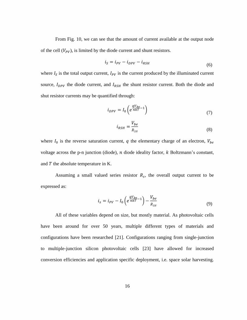
From Fig. 10, we can see that the amount of current available at the output node
of the cell (𝑉𝑃𝑉), is limited by the diode current and shunt resistors.
𝑖𝑆 = 𝑖𝑃𝑉 − 𝑖𝐷𝑃𝑉 − 𝑖𝑅𝑆𝐻 (6)
where 𝐼𝑆 is the total output current, 𝐼𝑃𝑉 is the current produced by the illuminated current
source, 𝐼𝐷𝑃𝑉 the diode current, and 𝐼𝑅𝑆𝐻 the shunt resistor current. Both the diode and
shut resistor currents may be quantified through:
𝑖𝐷𝑃𝑉 = 𝐼0 (𝑒
𝑞𝑉𝑏𝑒𝑛𝑘𝑇
−1) (7)
𝑖𝑅𝑆𝐻 =
𝑉𝑏𝑒
𝑅𝑆𝐻
(8)
where 𝐼0 is the reverse saturation current, 𝑞 the elementary charge of an electron, 𝑉𝑏𝑒
voltage across the p-n junction (diode), 𝑛 diode ideality factor, 𝑘 Boltzmann’s constant,
and 𝑇 the absolute temperature in K.
Assuming a small valued series resistor 𝑅𝑠, the overall output current to be
expressed as:
𝑖𝑠 = 𝑖𝑃𝑉 − 𝐼0 (𝑒
𝑞𝑉𝑏𝑒𝑛𝑘𝑇
−1) −𝑉𝑏𝑒
𝑅𝑆𝐻
(9)
All of these variables depend on size, but mostly material. As photovoltaic cells
have been around for over 50 years, multiple different types of materials and
configurations have been researched [21]. Configurations ranging from single-junction
to multiple-junction silicon photovoltaic cells [23] have allowed for increased
conversion efficiencies and application specific deployment, i.e. space solar harvesting.
17
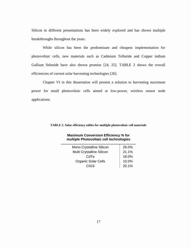
Silicon in different presentations has been widely explored and has shown multiple
breakthroughs throughout the years.
While silicon has been the predominant and cheapest implementation for
photovoltaic cells, new materials such as Cadmium Telluride and Copper indium
Gallium Selenide have also shown promise [24, 25]. TABLE 2 shows the overall
efficiencies of current solar harvesting technologies [26].
Chapter VI in this dissertation will present a solution to harvesting maximum
power for small photovoltaic cells aimed at low-power, wireless sensor node
applications.
TABLE 2. Solar efficiency tables for multiple photovoltaic cell materials
Maximum Conversion Efficiency % for multiple Photovoltaic cell technologies
Mono Crystalline Silicon 26.0%
Multi Crystalline Silicon 21.1%
CdTe 18.0%
Organic Solar Cells 10.0%
CIGS 20.1%

18
Radiofrequency harvesting
The capability of transferring power wirelessly has been a goal which has been
aimed for since the beginning of electrical power. Pioneers such as Nikola Tesla
envisioned the transmission of electrical power wirelessly as a means for global
reconciliation [27]. Power transmission through electromagnetic waves would allow a
near unlimited source of available power from the environment. This would allow for
applications which could potentially do completely without an on-board battery [28].
Applications in various fields can be reached: display technology, biomedical sensors,
and wireless networks would allow for both complex and compact electronic solutions to
become commonplace in everyday lives.
Previous works on near-field magnetic resonance [29] and inductive coupling
[30] solutions are considered near-field solutions. Far-field power transmission through
RF/microwave energy transmission presents itself as the viable option to fulfill the
power transmission challenge; with solutions combining solar harvesting in space and
then converting harvested power to microwaves beamed down to earth [31, 32] to low
power radiofrequency ID (RFID) tags working with 𝜇𝑊 of power [33].
Fig. 11 shows an overall radiofrequency (RF) energy harvesting system. The
system is made up of a Power Transmitter which generates the power to be transmitted,
efficiency and power to be transmitted stand out as the main limitations in this block.
Depending on the application, antennas are chosen which meet directionality and
polarization.

19
Fig. 11. RF energy harvesting system.
Once the power is transmitted through the medium, the RF energy harvesting
node takes the available RF power and converts it to stored power.
As RF harvesting is aimed at far-field applications, power must be extracted from
the air at increasingly low power densities. This is due to the propagation energy
dropping off rapidly as distance from the source increase [34]. In free space both electric
field and power densities drop off at a rate of 1/𝑑2, with 𝑑 being the distance from the
power transmitting source. This signifies that 6 dBs of power are lost for every doubling
of the distance from transmitter, causing serious strain on the receiving energy
harvesting node block.
The components making up the node are: receiving antenna, matching network,
AC-DC rectification block, and finally a Storage block [18]. As shown in Fig. 11, the
antenna picks up the radiated power from the power transmitter, the matching network
operates to ensure maximum power is transferred to the system, the AC-DC rectification
converts the incoming RF signal to a DC voltage while performing a DC voltage gain,
RF
Transmitter
Matching
network
AC-DC
RectificationStorage
Energy Harvesting NodePower
Transmitter
Antennas
Transmitted
Power

20
and finally the Storage block comprised of a storage element such as capacitor or
battery.
Implementation of the matching network is usually performed with off-chip
inductors and capacitors, ensuring high quality factors (Q) and low parasitic resistance
values. A drawback of having a high valued Q is the limitation in harvested bandwidth
over which the system may operate as shown:
𝑄 = 𝜔 ∙ (
𝐸𝑛𝑒𝑟𝑔𝑦 𝑆𝑡𝑜𝑟𝑒𝑑
𝐴𝑣𝑒𝑟𝑎𝑔𝑒 𝑃𝑜𝑤𝑒𝑟 𝐷𝑖𝑠𝑠𝑖𝑝𝑎𝑡𝑒𝑑) → 𝑄 =
𝑓𝑐
Δ𝑓
(10)
where 𝜔 is the tuned frequency of the matching network, 𝑓𝑐 the center frequency of
operation and Δ𝑓 the system bandwidth.
Both the antenna impedance matched to the input impedance of the rectifier
circuit will allow for best operational performance for the system. Matching allows for
passive amplification of the signal to reduce stress on the AC-DC block.
Fig. 12 shows an individual AC-DC rectification block. As RF power enters the
rectifier, it is rectified and delivered to the DC output node during the positive half-
cycle. While at the negative half-cycle, the voltage is clamped through the input
capacitor 𝐶𝑖𝑛 to the maximum voltage achieved during the positive half-cycle. Fig. 13
shows the aforementioned operation of the rectifying block.

21
Fig. 12. AC-DC rectifier.
Fig. 13. Positive and negative half-cycle performance for RF AC-DC rectifier.
DC Output
RF Input
Cin
DC Output
DC Output
+-
+-
Cin
Cin
22
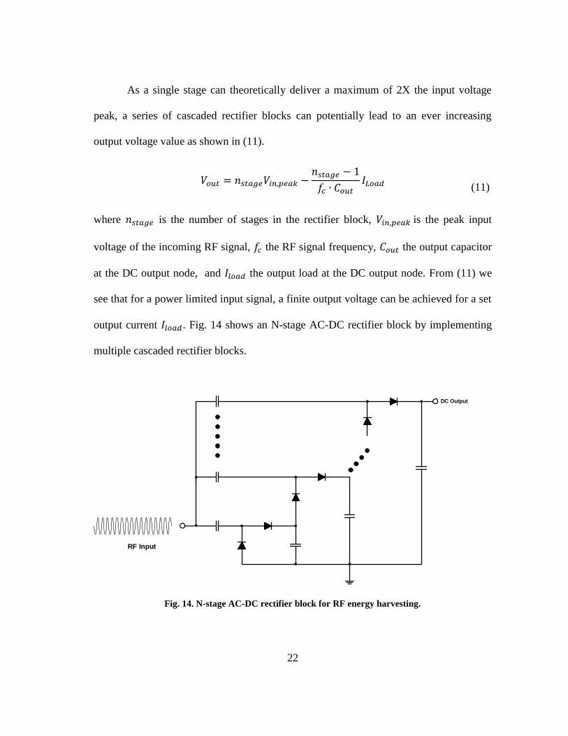
As a single stage can theoretically deliver a maximum of 2X the input voltage
peak, a series of cascaded rectifier blocks can potentially lead to an ever increasing
output voltage value as shown in (11).
𝑉𝑜𝑢𝑡 = 𝑛𝑠𝑡𝑎𝑔𝑒𝑉𝑖𝑛,𝑝𝑒𝑎𝑘 −
𝑛𝑠𝑡𝑎𝑔𝑒 − 1
𝑓𝑐 ∙ 𝐶𝑜𝑢𝑡𝐼𝐿𝑜𝑎𝑑
(11)
where 𝑛𝑠𝑡𝑎𝑔𝑒 is the number of stages in the rectifier block, 𝑉𝑖𝑛,𝑝𝑒𝑎𝑘 is the peak input
voltage of the incoming RF signal, 𝑓𝑐 the RF signal frequency, 𝐶𝑜𝑢𝑡 the output capacitor
at the DC output node, and 𝐼𝑙𝑜𝑎𝑑 the output load at the DC output node. From (11) we
see that for a power limited input signal, a finite output voltage can be achieved for a set
output current 𝐼𝑙𝑜𝑎𝑑. Fig. 14 shows an N-stage AC-DC rectifier block by implementing
multiple cascaded rectifier blocks.
Fig. 14. N-stage AC-DC rectifier block for RF energy harvesting.
RF Input
DC Output

23
It should be noted that (11) does not take into account the forward bias voltage
drops of the diodes in the rectifier. This reduces overall efficiency of the harvester by
limiting the delivered power at the output node (DC output).
Implementing CMOS transistors as diodes helps alleviate the forward bias drop
issue to an extent [18, 35], but are still a major bottleneck in RF harvesting technology
and the minimum power needed for scavenging purposes; Fig. 15 shows both
implementations.
Fig. 15. Diode and NMOS implementation of AC-DC rectifier block for RF harvesting.
Diode
Implementation
NMOS
Implementation

24
Fig. 16. Schematic of three types of electromechanical transducers a) electrostatic b) electromagnetic
and c) piezoelectric.
Current limits for state-of-the-art harvesting sensitivity are ~ 25 dBm of input
power for a 1.3 GHz RF frequency [36].
Kinetic energy harvesting
Focusing on the vibration energy available, we can see that vibration sources are
generally ubiquitous and can be readily found in accessible locations such as air ducts
and building structures. There are generally three types of electromechanical transducers
that can convert vibration energy to electrical energy, these are: electrostatic,
electromagnetic and piezoelectric and are shown in the figure below.
Out of the three different option for harvesting kinetic energy it is the
piezoelectric device the one that has been more extensively studied and presents many
advantages over the other two mechanisms, such as: simple configuration, high
conversion efficiency and better control.
Spring, k
Wire coil, I
mass, m
Permanent
magnet, B
+-
+-+-
P
P
ForceV
+
-
a) b) c)

25
Fig. 17. Piezoelectric effect showing ceramic cation and anion reconfiguration with both external
polarization voltage and deformation forces applied.
The manner in which piezoelectric materials operate is that they become
electrically polarized, or undergo a change in polarization in their structure, when
subjected to mechanical deformation (stress or changes in its original dimensions). This
results in a variation in bond lengths between cations and anions, this may cause a flow
of energy to occur if a closed circuit system is implemented [37]. Fig. 17 illustrates the
aforementioned occurrence.
This phenomenon was discovered on many crystals, for instance, tourmaline,
topaz, quartz, Rochelle salt, and cane sugar, by Jacques and Pierre Curie brothers in
1880, and named as piezoelectricity or piezoelectric effect, which describes a
relationship between stress and voltage. Conversely, a piezoelectric material will have a
change in dimension when it is exposed in an electric field. This inverse mechanism is
called electrostriction (Fig. 17). Those devices utilizing the piezoelectric effect to
-
+
-
+
-
+
-
+
-
+
-
+
Force
+
-
VpolarizationVpolarization
-
+
-
+
-
+
-
+
-
+
Piezoelectric ceramic
before polarization
voltage or physical
deformation
26
convert mechanical strain into electricity are called transducers, which can be used in
sensing applications, such as sensors, microphones, and strain gages.
While those devices utilizing the inverse piezoelectric effect to generate a
dimension change by adding an electric field are called actuators and used in actuation
application, such as positioning control devices, and frequency selective device.
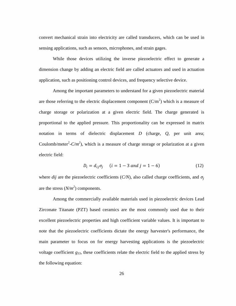
Among the important parameters to understand for a given piezoelectric material
are those referring to the electric displacement component (C/m2) which is a measure of
charge storage or polarization at a given electric field. The charge generated is
proportional to the applied pressure. This proportionality can be expressed in matrix
notation in terms of dielectric displacement D (charge, Q, per unit area;
Coulomb/meter2-C/m
2), which is a measure of charge storage or polarization at a given
electric field:
𝐷𝑖 = 𝑑𝑖𝑗𝜎𝑗 (𝑖 = 1 − 3 𝑎𝑛𝑑 𝑗 = 1 − 6) (12)
where dij are the piezoelectric coefficients (C/N), also called charge coefficients, and 𝜎𝑗
are the stress (N/m2) components.
Among the commercially available materials used in piezoelectric devices Lead
Zirconate Titanate (PZT) based ceramics are the most commonly used due to their
excellent piezoelectric properties and high coefficient variable values. It is important to
note that the piezoelectric coefficients dictate the energy harvester's performance, the
main parameter to focus on for energy harvesting applications is the piezoelectric
voltage coefficient g33, these coefficients relate the electric field to the applied stress by
the following equation:

27
𝑔33 =
𝑑33
𝜀𝑜 ∙ 𝐾3
(13)
where 𝜀𝑜 is the permittivity of free space and K3 is the relative dielectric constant of the
material. Higher g33 values yield higher output voltages. This coefficient is low for bulk
PZT ceramics due to their high K3. However, g33 can be increased by incorporating the
PZT ceramic as continuous parallel rods in an inactive polymer matrix.
The application of an external force, 𝜎, to a piezo material creates an Electric
field, E, proportional to the voltage coefficient, g. This is expressed by the following
equation:
𝐸 = 𝑔 ∙ 𝜎 (14)
Considering that the electric field is given by 𝐸 =𝑉
𝐿 and 𝜎 =
𝐹
𝐴, we can assume
that the output voltage due to the applied force on the piezoelectric material is given by:
𝑉 =
𝑔 ∙ 𝐹 ∙ 𝐿
𝐴
(15)
where V is the voltage, F is the applied force, L and A are the length and cross section of
the device. From this equation we can see that for larger voltage coefficients, force and
length, along with small cross section gives us the best results in terms of output voltage.
Accordingly piezoelectric fibers give off higher voltages from high L/A ratios. Hence a
tradeoff is seen in terms of area and length, but it is the voltage coefficient which is the
main restriction in terms of good power conversion.

28
A second important factor in piezoelectric converters is the resonant frequency,
which limits the range of operational frequency the transducer possesses. Depending on
resonant frequency, a particular application driven design may be achieved.
Fig. 18. Piezoelectric energy harvester electrical model.
A first approach to the calculation of the resonant frequency is given by:
𝑓𝑟 =𝜔
2𝜋=
1
2𝜋√
𝐾
𝑚𝑒
(16)
where fr is the resonant frequency; ω is the angular frequency; K is the spring constant at
the tip of the cantilever, me is the effective mass of the cantilever. It can be easily seen
that for higher value of masses i.e. area, we can expect a much lower resonant frequency
for the device.
As the piezoelectric transducer bends in both directions during mechanical stress,
the electrical equivalent model behaves as an AC current source (𝐼𝑃𝑍𝑇) which charges
and discharges a capacitance across the material surface (𝐶𝑃𝑍𝑇). A leakage resistor is
also considered, 𝑅𝐿𝑒𝑎𝑘, causing some loss in the delivered charge.
IPZT CPZT RLeak
iPZT
+
-
VPZT
iPZT
IPeak
-IPeak

29
This dissertation does not deal with the power generated from kinetic energy
harvesting sources.
Alternative energy harvesting sources
Alternative approaches to generate power have been continuously researched in
hopes to reduce the dependency on fossil fuels. As mentioned throughout this chapter,
many of the energy harvesting technologies have the potential of reducing the carbon
footprint of humans. Taking an approach which considers biological substances as
potential sources of power is not entirely new; in the late 1700s, Luigi Galvani noted that
living beings possessed a capacity to generate electrical charges within the body. This
would lead researchers to look at microscopic sources for power: bacteria.
In 1911, the first paper published on the power generation capabilities of bacteria
were first reported [38]. This would lead to implementing groups of bacteria into cells to
better harness their power generation capacity. This led to the breakthrough of Microbial
Fuel Cells (MFC).
MFCs are a bioelectrochemical technology that converts chemical energy into
electrical energy by producing electricity directly from biodegradable substrates such as
wastewater; Fig. 19 shows a simplified schematic of the MFC. In MFCs, exoelectrogenic
bacteria break down the carbon substrates while producing electrons, which are then
transferred to the anode [39]; these electrons flow to the cathode through an external
load, and then combine with protons and oxygen to form water, thus completing a full
circuit and producing electricity.
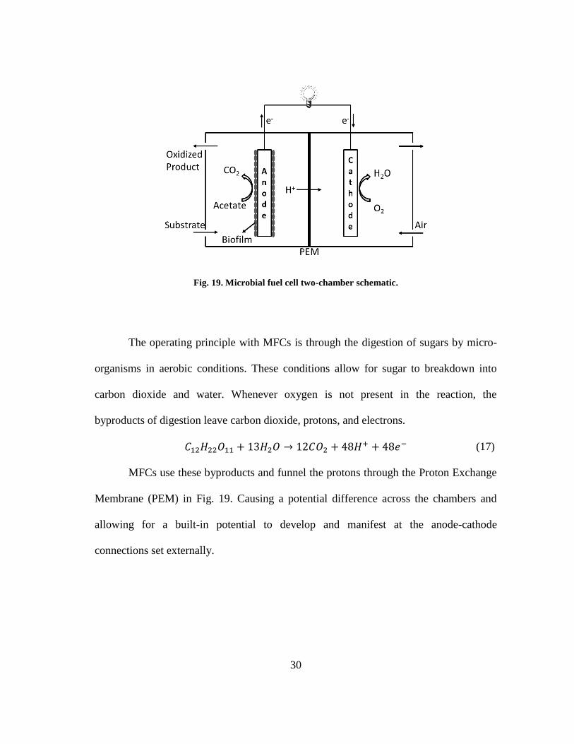
30
Fig. 19. Microbial fuel cell two-chamber schematic.
The operating principle with MFCs is through the digestion of sugars by micro-
organisms in aerobic conditions. These conditions allow for sugar to breakdown into
carbon dioxide and water. Whenever oxygen is not present in the reaction, the
byproducts of digestion leave carbon dioxide, protons, and electrons.
𝐶12𝐻22𝑂11 + 13𝐻2𝑂 → 12𝐶𝑂2 + 48𝐻+ + 48𝑒− (17)
MFCs use these byproducts and funnel the protons through the Proton Exchange
Membrane (PEM) in Fig. 19. Causing a potential difference across the chambers and
allowing for a built-in potential to develop and manifest at the anode-cathode
connections set externally.

31
Fig. 20. Output voltage of MFC vs. time.
The device must also possess the ability to oxidize the substrate being injected
into the chamber, through either an intermittent or continuous mechanism; otherwise the
system falls into the biobattery category. The defining characteristic of the MFC lies in
the catalyzed electron liberation at the anode and subsequent electron consumption at the
cathode, in a sustainable fashion.
Since the MFC technology is dependent on biological variables, non-linearity is
to be expected. As the substrate is completely consumed by the bacteria within the anode
chamber of the MFC, the exoelectrogenic activity within the chamber reduces. This
causes an output power degradation; thus, both the measured voltage and current are
reduced. Fig. 20 shows the tested performance for a two chamber MFC, with 240 mL
volume. It can be seen from this plot that on the 81st day, the output voltage abruptly
drops, until substrate replenishment is performed.

32
Fig. 21. Microbial fuel cell simplified electrical equivalent model.
This sets a limit to the applications in which the MFC technology can aid, a
common thread in all energy harvesting technology. Nevertheless, given the right
conditions and constant substrate replenishment application (water treatment plants),
MFCs can potentially lead to helpful power generation to reduce overall power demand
and load of a system.
A simplified electrical equivalent model of the MFCs is constructed in Fig. 21.
This first order model possesses a dynamic and steady-state power component. By
implementing the series resistor, 𝑅𝑀𝐹𝐶 , a maximum power capability is determined in
the MFC model. While the parasitic capacitor, 𝐶𝑀𝐹𝐶 , is used to model the dynamic
behavior of the MFC whenever a charging/discharging scenario is presented.
More complete electrical equivalent models consider multiple variables [40], i.e.
pH, temperature, and concentration. Nonetheless, for first order approximation electrical
model, from Fig. 21, offers sufficient information for proper PMU design. Chapters IV,
VsVMFC
RMFC
CMFC

33
V and VI in this dissertation will present a solution to harvesting maximum power for
MFCs aimed at low-power, wireless sensor node applications.
Voltage regulators
As the energy harvesting transducers offer unregulated voltage, the need for
regulators is a must. Since the power produced by the transducers is non-continuous and
at times extremely sparse. The need for power conditioners capable of storing and later
delivering the stored energy to electrical loads on demand becomes apparent.
The implemented regulators must be highly efficient, as well as low-power in
order to deliver the vast majority of the harvested power to the load. This is shown as:
𝜂𝑒𝑓𝑓 =
𝑃𝐿𝑜𝑎𝑑 − 𝑃𝑙𝑜𝑠𝑠𝑒𝑠 − 𝑃𝑐𝑜𝑛𝑠𝑢𝑚𝑒𝑑
𝑃𝑖𝑛𝑝𝑢𝑡
(18)
From (18) we see that the overall efficiency depends on both losses and
consumed regulator power, this becomes a major issue when the input power, 𝑃𝑖𝑛 is
extremely small to begin with. Two major topologies of power converters will be briefly
described and overviewed to better understand the major benefits and drawbacks with
each topology: switching regulators and linear regulators.
Inductive switching regulators
Switching regulators are a category of regulator that implement magnetic-based
components (inductor) to draw, store, and then release charge to an electronic load. This
is achieved by temporarily energizing and de-energizing inductors in alternating cycles.

34
As see in Fig. 22, the input inductor, 𝐿𝑖𝑛, draws current from the input source by
connecting 𝐿𝑖𝑛 to the input source, 𝑉𝑖𝑛, to one terminal and the second terminal to a
lower potential. This causes the inductor current, 𝑖𝐿𝑖𝑛, to increase in a proportional
manner as the waveform in Fig. 22b shows (blue). The almost linear current increase is
due to the inductor voltage is determined by:
𝑉𝐿𝑖𝑛 = 𝐿𝑖𝑛
𝑑𝑖𝐿𝑖𝑛
𝑑𝑡= 𝑉𝑖𝑛
(19)
Fig. 22. A) Switching phases and B) inductor current waveform of an inductive switching regulator.
During the complementary cycle 𝑉𝐿𝑖𝑛 is subjected to the output voltage, 𝑉𝑜𝑢𝑡,
which effectively causes a reverse polarity across 𝐿𝑖𝑛. This causes the inductor to release
energy which was received in the first cycle (Fig. 22B).
Since 𝑉𝑜𝑢𝑡 is usually regulated to a set level, the output voltage is usually
constant and well defined. This causes 𝐿𝑖𝑛 to discharge at a rate of −𝑉𝑜𝑢𝑡/𝐿𝑖𝑛. Both the
ViniLin
iLin
Lin
Lin Vout
Vin-0Lin
0-Vout
Lin
iLin <avg>
Cout Rout
Vout
Cout RoutVin
T2
T1
T1
T2

35
input and output voltage define the inductor current ripple and amount of energy
delivered to the load.
Since the output current to be delivered should be continuous, the inductor ripple
current sits above a steady-state averaged DC current value given by 𝑖𝐿𝑖𝑛<𝑎𝑣𝑔>.
Depending on the load demands, the inductor ripple current may ride on a high valued
steady-state value, or the current ripple may reach zero amps during the discharging
cycle, before the next charging cycle. The value of the inductor ripple current prior to the
next charging cycle defines whether the switching converter operates in Continuous
Conduction Mode (CCM) or Discontinuous Conduction Mode (DCM). Both of these
modes of operation are further discussed in Chapter II.
A second feature which is integral to inductive switching converters is the ability
to produce a higher (boost) or lower (buck) voltages. These higher or lower voltages can
be achieved as long as the charging and discharging cycles of 𝐿𝑖𝑛 remain positive and
negative, respectively. This since in order for 𝐿𝑖𝑛 to release the stored charge to the load,
requires the differences across its terminals for correct charging/discharging.
The inductors used in switching regulators allow for continuous current by
instantly varying its voltage until an adequate supply or load is found for its stored
charge. Any switch resistance or inductor DC resistance, 𝑅𝑠𝑒𝑟𝑖𝑒𝑠, exhibited in the
converter will drop a root-mean-square voltage, dissipating the following expression:
𝑃𝑅 = 𝐼𝐿𝑖𝑛(𝑟𝑚𝑠)2 ∙ 𝑅𝑠𝑒𝑟𝑖𝑒𝑠
(20)

36
Since the associated DC resistances are usually low, inductive switching
converter offer high values of efficiency. The conduction losses (𝑃𝑅) while low are not
zero, and are proportional to the input current squared. Increasing this current will also
increase the amount of power burnt on these resistors, increasing conduction losses.
Capacitive switching regulators
The capacitive switching regulator, or more commonly known Charge Pump,
implements the same principle as the inductive switching regulator but instead of using a
magnetic component for charge storage, a capacitor is used. Both buck and boost
operations are possible with charge pumps.
Fig. 23. Operation and switching waveforms for a simple voltage doubler.
Φ1
Φ1 C1
V1
Φ2 C1
V1
Φ2 VoutVout
Φ1
Φ2 Φ1 C1 Vin
V1Φ2
Cout
Vout
V1
1Vin
2Vin
T1 T2
T1 T2T2
Vin Vin

37
Compared with inductive switching regulators, charge pumps offer an alternative
to designs where the use of magnetic components is not desired. Offering a fully
integrated approach is also an added bonus to using charge pumps as voltage regulators
for applications. Fig. 23 shows the operation and waveform of the intermediate node in a
simple voltage doubler topology.
During 𝜙1 the “flying” capacitor 𝐶1 is charged up to 𝑉𝑖𝑛, while the output voltage
𝑉𝑜𝑢𝑡 in capacitor 𝐶𝑜𝑢𝑡 remains static.
𝑄𝐶1 = 𝑉𝑖𝑛 ∙ 𝐶1 (21)
During 𝜙2, the flying capacitor is placed in series with 𝑉𝑖𝑛, and the addition of
both these voltages delivers a 2X increment to 𝑉𝑜𝑢𝑡 (now in parallel with the series 𝐶1
and 𝑉𝑖𝑛).
𝑄𝐶1 = (𝑉𝑜𝑢𝑡 − 𝑉𝑖𝑛) ∙ 𝐶1 = 𝑉𝑖𝑛 ∙ 𝐶1 → 𝑉𝑜𝑢𝑡 = 2 ∙ 𝑉𝑖𝑛 (22)
Multiple topologies can be implemented with the flying capacitor topologies
[41], going from parallel-series (Fig. 23) for step-up operations, as well as series-parallel
for step-down voltages.
Nonetheless, the main limitations of charge pumps are the required area for the
desired application, capacitor density areas in integrated CMOS processes are low and
lossy (high ESR and leakage) compared to discrete components, output noise due to
constant switching of capacitors, and output current delivering capability [41]. For
higher current delivering densities (low output resistance of charge pump) a higher
capacitance value is required [42]:

38
𝑅𝑜𝑢𝑡 =
𝑁
𝐶𝑠𝑡𝑎𝑔𝑒 ∙ 𝑓𝑠𝑤𝑖𝑡𝑐ℎ𝑖𝑛𝑔
(23)
where 𝑁 is the number of stages in the charge pump topology, 𝐶𝑠𝑡𝑎𝑔𝑒 is the flying
capacitance value, and 𝑓𝑠𝑤𝑖𝑡𝑐ℎ𝑖𝑛𝑔 is the switching frequency of the charge pump. Due to
these limitations, charge pumps are widely used in internal CPU memories and solid-
state drives which require high-voltage pulses to program and erase data. Other
applications for charge pumps are found in LED drivers, where high voltages are
required while sacrificing minimum area.
Linear regulators
Fig. 24. Linear regulator simplified schematic.
Rlinear
RLoad
Vout =
Linear Regulator
Vin
𝑽𝒊𝒏 𝑹𝑳𝒐𝒂𝒅
𝑹𝑳𝒐𝒂𝒅 + 𝑹𝑳𝒊𝒏𝒆𝒂𝒓

39
The linear regulator is, at its name dictates, a linearly dependent variable that
delivers a constant output voltage from a higher input voltage. Fig. 24 shows a
simplified representation of the operational principle of linear regulators. As 𝑉𝑖𝑛 or
𝑅𝐿𝑜𝑎𝑑 change, the variable resistor 𝑅𝑙𝑖𝑛𝑒𝑎𝑟 varies its value in order to maintain 𝑉𝑜𝑢𝑡
constant.
The implementation of 𝑅𝑙𝑖𝑛𝑒𝑎𝑟 is usually implemented through a semiconductor
transistor, who’s conductance is modulated through a control loop to maintain 𝑉𝑜𝑢𝑡
constant. Due to the low number of transistors in the overall implementation of the
regulator, it is able to react quickly to load demands as well as having limited quiescent
power consumption. This circuit generates minimum noise to the output load (not
counting thermal noise) since it is not periodically switching between fully on and off
stages [43].
The main limitation in this type of approach to regulation is voltage flexibility.
For a linear regulator 𝑉𝑖𝑛 will always be greater than 𝑉𝑜𝑢𝑡, a case which is not so in
inductive or capacitive switching regulators. Also, the energy harvesting transducer and
output storage (capacitor) set the voltage across 𝑅𝑖𝑛, which means that the power lost in
the linearly variable resistor rises linearly with input current. This sets maximum
efficiency of the regulator as a function of the dropout voltage (voltage drop across 𝑅𝑖𝑛).
𝜂𝐿𝐷𝑂 =
𝑃𝑜𝑢𝑡
𝑃𝑖𝑛=
𝑃𝑜𝑢𝑡
𝑃𝑜𝑢𝑡 + 𝑃𝐿𝑜𝑠𝑠
=𝑉𝑜𝑢𝑡 ∙ 𝐼𝑜𝑢𝑡
𝑉𝑜𝑢𝑡 ∙ 𝐼𝑜𝑢𝑡 + (𝑉𝑖𝑛 − 𝑉𝑜𝑢𝑡) ∙ 𝐼𝑜𝑢𝑡=
𝑉𝑜𝑢𝑡
𝑉𝑖𝑛
(24)

40
From (24), if the input voltage were to be 15 V and the output 2.5 V, the overall
regulator efficiency would fall to ~17%. This would mean that approximately 83% of the
input power is spent on 𝑅𝑖𝑛. This also signifies that the linear regulator is extremely
highly efficient for 𝑉𝑜𝑢𝑡 values close to 𝑉𝑖𝑛. Also, linear regulators possess superior
noise rejection, mainly due to the lack of switching components when compared to the
switching regulator counterparts.
Energy storage elements
Having a place to store the harvested power from the energy harvesting sources
is a critical component in any power management solution. Solutions range from
batteries, to temporary storage units such as capacitors.
Breakthroughs are performed at a rapid rate in both battery technology [44, 45]
and capacitor technology in the form of supercapacitors/ultracapacitors [46, 47].
Although both components offer their respective benefits to temporary storage, the main
difference between both technologies is the power/energy density availability. Whereas
capacitor technologies possess a much higher power delivery density, delivering high
current values in an instantaneous fashion; battery technology offers a more energy
dense solutions, capable of delivering steady amounts of energy over longer periods of
time. Fig. 25 shows a conceptual comparison between both power and energy densities.
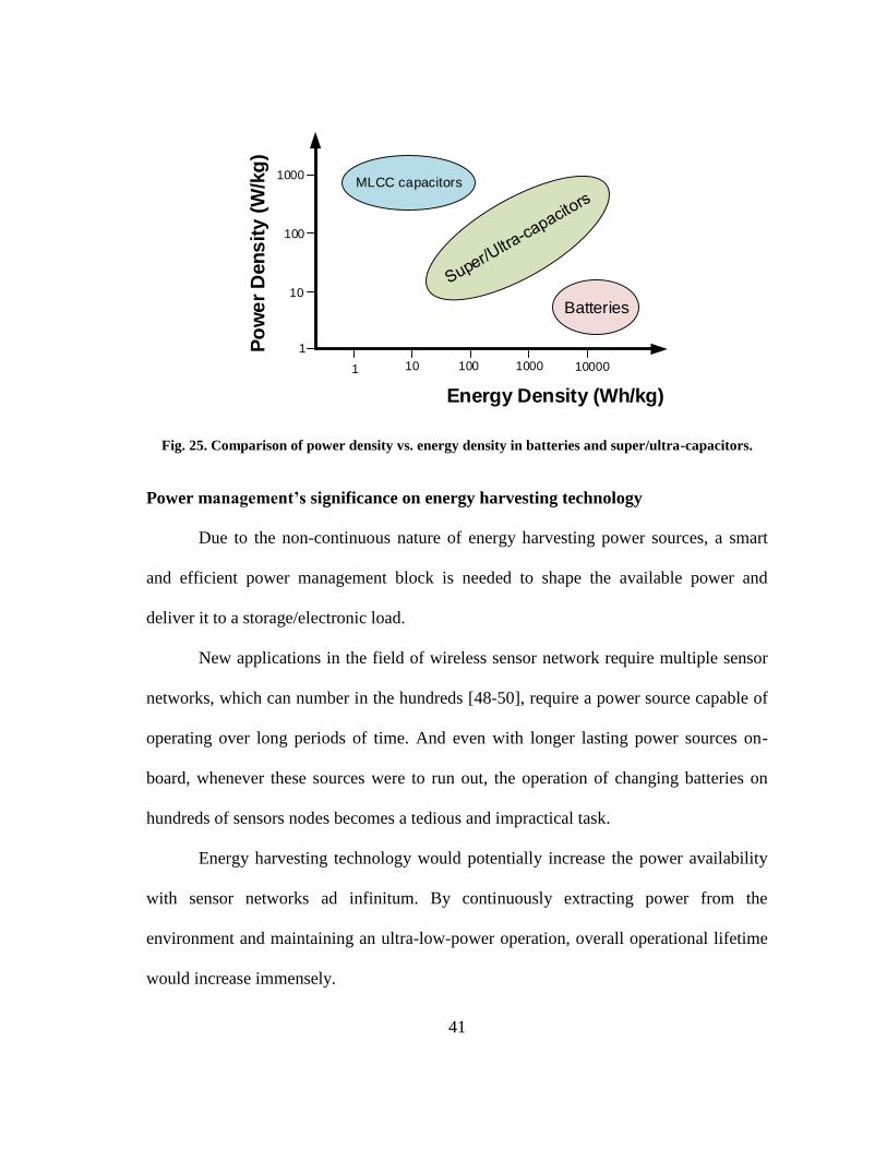
41
Fig. 25. Comparison of power density vs. energy density in batteries and super/ultra-capacitors.
Power management’s significance on energy harvesting technology
Due to the non-continuous nature of energy harvesting power sources, a smart
and efficient power management block is needed to shape the available power and
deliver it to a storage/electronic load.
New applications in the field of wireless sensor network require multiple sensor
networks, which can number in the hundreds [48-50], require a power source capable of
operating over long periods of time. And even with longer lasting power sources on-
board, whenever these sources were to run out, the operation of changing batteries on
hundreds of sensors nodes becomes a tedious and impractical task.
Energy harvesting technology would potentially increase the power availability
with sensor networks ad infinitum. By continuously extracting power from the
environment and maintaining an ultra-low-power operation, overall operational lifetime
would increase immensely.
Po
we
r D
en
sit
y (
W/k
g)
Energy Density (Wh/kg)
MLCC capacitors
Batteries
1
10
100
1000
1 10 100 1000 10000

42
Proposed solution
This dissertation presents four unique power management solutions Energy
Harvesting sources. Implementing inductive, capacitive and linear regulator approaches;
the focus of extracting maximum power as well as delivering a regulated load are
tackled in the proposed approaches.
The first part of the dissertation focuses on the application of inductive switching
regulators and their use in energy harvesting applications. In the first work, a built-in
input matching technique capable of handling a wide variation of multi-array TEG
impedances ranging two decades, from 10s to 1000s of ohms is presented. Maximum
power point tracking (MPPT) control for a boost converter (BC) are performed to assure
maximum power transfer. A prototype was fabricated in 0.5 μm CMOS with the
achieved goal of maximum measured efficiency of over 60% for an RTEG=33.33Ω, and
quiescent power consumption under 1µW. Fig. 26 shows the conceptual solution of the
harvesting unit.

43
Fig. 26. Proposed solution for TEG array impedance matching and energy harvesting.
The second work focuses on extracting maximum power from MFCs. Due to the
MFC’s low power and voltage production, a power management system (PMS) is
required to process the MFC power to a more readily usable level. For this application a
monolithic PMS with an integrated maximum power extraction algorithm (MPEA) is
presented. The MPEA will allow for quick and accurate pin-pointing of the matching
conditions for maximum power transfer from the MFC to the PMS. The PMS was
fabricated and tested in 0.5 μm CMOS technology. The maximum dynamic efficiency
was measured at ~58%. Fig. 27 shows the conceptual solution of the harvesting unit.

44
Fig. 27. Proposed solution for MFC source impedance matching and energy harvesting.
The second part of the proposal focuses on a more fully integrated approach by
implementing switched capacitor regulators. A second solution targeted for MFC
applications is presented via an inductorless DC-DC (I-DCDC) converter for an energy-
aware power management unit (EA-PMU). The system is capable of performing a DC
step-up gain of up to 10X and achieving MPPT efficiently. The converter is a key
building block for an EA-PMU capable of identifying the best candidate for energy
harvesting from an array of MFCs.
Vout
Csuper RLoad
L1 Boost
Converter
Cin
Vdc
Impedance Tracking
fs
VCO
LVRVswMFC
MPEA
TP
ZCSTVsw
Zero Current Switching
Delay Cell

45
Due to the MFC’s varying power profile over time, identifying and selecting the
best MFC from an array enhances efficiency and overall power delivery. MPPT is
achieved through wide variety of impedance scenarios from the MFC array while
maintaining low power consumption. The converter was designed, fabricated, and tested
in 0.18 μm CMOS process and achieved a maximum efficiency of 65%. Fig. 28 shows
the conceptual solution of the harvesting unit.
Fig. 28. Proposed solution for MFC array impedance matching and energy harvesting.
Finally an autonomous, fully integrated, Energy Harvesting power management
unit (PMU) with digital regulation for Internet of Things (IoT) applications is presented.

46
The main focus of this work is targeted for wireless sensor node applications, and
focus on performing maximum power extraction and storing harvested power. Efforts on
delivering a regulated supply to noise sensitive blocks have yet to be fully achieved with
current solutions. The presented PMU achieves full autonomous operation able to
perform maximum power point tracking (MPPT) for DC type energy harvesting sources
(solar, thermal, biomass), startup operation with the available power from the harvesting
source, and deliver a regulated output voltage through a digital Low dropout (LDO)
regulator. The system was fabricated in 0.18 μm CMOS process and maximum end-to-
end efficiency was measured to be at 57 % with 1.75 mW of input power. Fig. 29 shows
the conceptual solution of the autonomous power management unit.
Fig. 29. Proposed solution for DC energy harvesting autonomous power management unit.

47
CHAPTER II
FUNDAMENTALS OF POWER MANAGEMENT SYSTEMS FOR ENERGY
HARVESTING
Introduction
Nowadays, commercially available consumer electronics possess a wide variety
of voltage/current level requirements that cannot be met with a single battery.
Implementing each and every one of the voltage domains would require the same
number of batteries, making the solution impractical. The answer lies in power
processing circuits capable of delivering multiple voltage/current domains with a single
source. As can be seen in Fig. 30, the main focus of these power processing circuits is to
convert one power domain, usually input voltage/current levels incompatible with the
required levels, to other more compatible voltage/current levels for the required
application.
Fig. 30. Switching converter power conversion illustration.
Switching
Converter
Rin Rout
Load
Source Load
Power
Conversion
Vin
iin iout
+
-
V1
+
-
V2

48
A key component in these types of conversions is the switching converter. The
switching converter operates by storing the input energy temporarily in magnetic field
storage components (inductive, transformers) or electric field storage components
(capacitors), then delivering the stored energy to the output load of the converter. This
stored/deliver cycle is repeated multiple times to achieve the required output voltage
level.
Akin to the switching converter, an alternative exists in the linear regulator. The
linear regulator operates as a variable resistor, as shown in Fig. 31; the resistor varies its
value in order to maintain a constant output voltage at 𝑉𝑜𝑢𝑡 when load demands vary.
Whereas the switching converter possesses a great flexibility in terms of load power
delivery, the linear regulator is a more limited topology since it can only deliver output
voltages below that of the input. Nonetheless, while the switching converter does
possess a high degree of freedom in terms of output power delivery the required
controller is higher in complexity when compared to the linear regulator.
When the variable resistor is implemented via an active device, i.e. a transistor, a
special type of linear regulator is implemented, named a Low Dropout Regulator due to
the low voltage drop across the Drain-Source (Collector-Emitter) terminals of the
device.
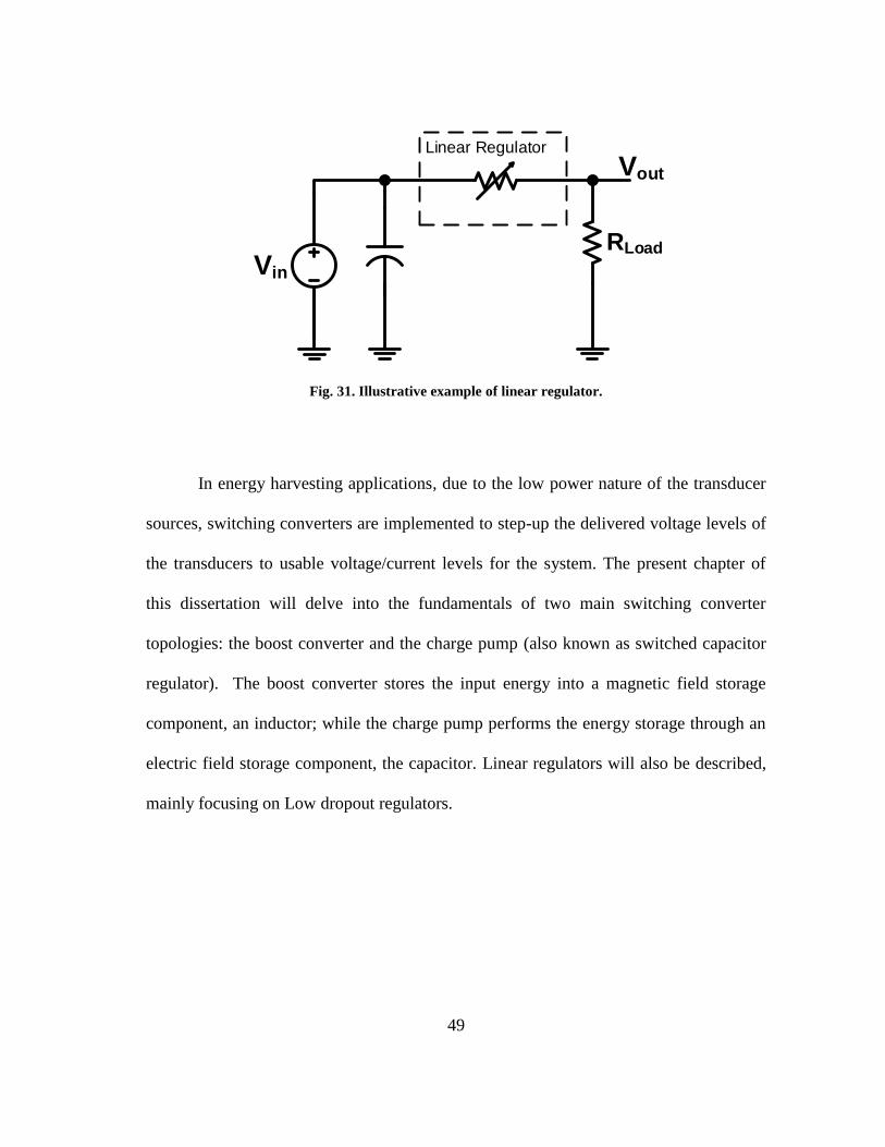
49
Fig. 31. Illustrative example of linear regulator.
In energy harvesting applications, due to the low power nature of the transducer
sources, switching converters are implemented to step-up the delivered voltage levels of
the transducers to usable voltage/current levels for the system. The present chapter of
this dissertation will delve into the fundamentals of two main switching converter
topologies: the boost converter and the charge pump (also known as switched capacitor
regulator). The boost converter stores the input energy into a magnetic field storage
component, an inductor; while the charge pump performs the energy storage through an
electric field storage component, the capacitor. Linear regulators will also be described,
mainly focusing on Low dropout regulators.
Vin
RLoad
Vout
Linear Regulator
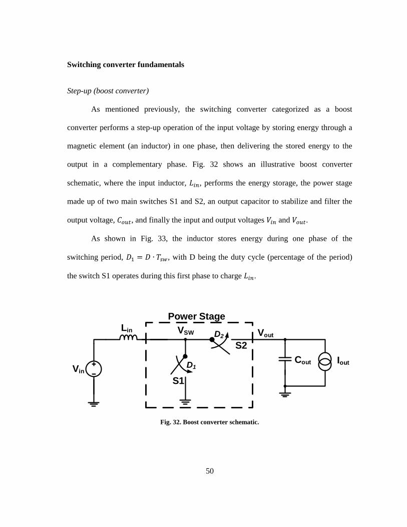
50
Switching converter fundamentals
Step-up (boost converter)
As mentioned previously, the switching converter categorized as a boost
converter performs a step-up operation of the input voltage by storing energy through a
magnetic element (an inductor) in one phase, then delivering the stored energy to the
output in a complementary phase. Fig. 32 shows an illustrative boost converter
schematic, where the input inductor, 𝐿𝑖𝑛, performs the energy storage, the power stage
made up of two main switches S1 and S2, an output capacitor to stabilize and filter the
output voltage, 𝐶𝑜𝑢𝑡, and finally the input and output voltages 𝑉𝑖𝑛 and 𝑉𝑜𝑢𝑡.
As shown in Fig. 33, the inductor stores energy during one phase of the
switching period, 𝐷1 = 𝐷 ∙ 𝑇𝑠𝑤, with D being the duty cycle (percentage of the period)
the switch S1 operates during this first phase to charge 𝐿𝑖𝑛.
Fig. 32. Boost converter schematic.
VoutLin
S1
S2
VSW
Power Stage
Vin
CoutD1
D2
Iout

51
Once the phase duration ends, S1 shuts off and S2 switches on, causing 𝐿𝑖𝑛 to
deliver the stored energy from the first phase to load. This secondary phase, 𝐷2 =
(1 − 𝐷) ∙ 𝑇𝑠𝑤, sees the delivered energy to the output load and once 𝐷2 is over, 𝐷1
begins anew and the cycle repeats.
Both switches S1 and S2 are implemented through active components. Shown in
Fig. 34 is a simplified schematic of the boost converter power stage with two different
switch implementations: Asynchronous and Synchronous. For the asynchronous case,
Fig. 34A, the switch network implemented via a transistor and diode: an NMOS
transistor for S1, and an output diode 𝑆𝐷 for S2. For the synchronous case, Fig. 34B,
both switches are implemented via transistors: an NMOS transistor for S1, and a PMOS
transistor for S2.
Fig. 33. Boost converter complementary phase operation.
VoutLin
S1
S2
VSW
Power Stage
Vin
CoutD1IoutiLin
Vout
Lin
S1
S2
VSW
Power Stage
Vin
Cout
D2
IoutiLin
iLin
Vout
D2
D1
icout
-Iout
iLin-Iout
out
out
C
I-
out
out
out
Lin
C
I
C
i
in
in
L
V
in
outin
L
VV

52
Fig. 34. A) Asynchronous boost converter schematic and B) synchronous boost converter schematic.
As asynchronous converters suffer from the forward bias drop of the diode, 𝑆𝐷,
they have an inherent reduced overall efficiency. The synchronous converters possess a
much higher efficiency due to the transistor voltage drop being much less than that of the
diode, but require a much more complex control in order to avoid having the S2 switch
on for too long, causing a backflow of current to the input.
Depending on load demands, the boost converter is able to operate under two
different modes: Continuous Conduction Mode (CCM) or Discontinuous Conduction
Mode (DCM). CCM applications are usually implemented for heavy-load currents at the
output voltage, whereas DCM applications are intended for more light-load applications.
L1
Asynchronous
Converter
VoutLin
NMOS
VSW
Power Stage
VN
Vin
D1
Cout
L1
Synchronous
Converter
VoutLin
NMOS
VSW
Power Stage
VN
Vin
Cout
PMOS
VP
Iout
Iout
A
B

53
Due to the load demand at the output, each operating mode has a distinctive current
shape passing through 𝐿𝑖𝑛. While as in CCM mode the inductor current never reaches 0
A due to the high demand at the output, in DCM mode the inductor current falls to 0 A
before or at the end of each period. Fig. 35 highlights both operating modes and the
voltage nodes associated to the boost converter. A more detailed description of each
operating mode will follow.
Independent of the type of power stage implemented (asynchronous or
synchronous), or operation mode (CCM or DCM) design insights for steady state
dynamics are needed for correct modeling of the converter for voltage regulation
applications. The following section presents the modeling method for the converter
based on the Pulse Width Modulation (PWM) switch design.
Fig. 35. Boost converter CCM and DCM inductor current waveforms.
ILin
VSW
D1 D2D2
ILin
VSW
D1 D2D2
Vout VoutVout Vout
CCM Operating Mode DCM Operating Mode

54
Fig. 36. DC and small signal models for CCM and DCM PWM switch implementations.
Fig. 37.DCM operating mode view of switch activation and behavior during each cycle.
Power Stage
1 D
ia ic
ca
p
Power Stagepa
c
Re p(t)
A) B)
D1 D2D2
DCM Operating Mode
ILin
S1 S2 S1 S2
Switch
activation
Behaves as
consuming power
from input
Behaves as
delivering power
to output
Ipeak

55
Operating modes
A Pulse Width Modulation (PWM) switch model for each operating mode [51]
allows for a simplified design approach while maintaining the system’s characteristics.
Fig. 36 shows the PWM equivalent model for both CCM (Fig. 36A) and DCM (Fig.
36B) operating modes for the boost converter. Both S1 and S2 switches from Fig. 32 are
encompassed within the Power Stage dashed-line box and are replaced by a three
terminal block. The terminals are labeled as a (active) connects to the S1 switch, p
(passive) connects to the S2 switch, and c (common) is common node to both switches.
For the CCM operating mode variable D represents the steady-state duty cycle,
represents small AC variations of the duty cycle, and represents the complete duty
cycle including any DC component and AC variations. For the DCM operating mode the
averaged switch waveforms (Fig. 37) obey Ohm’s law, and are modeled by an effective
resistance Re and a power source p(t) delivering the dissipated power through Re to the
output. The averaged waveforms for S2 follow a power source characteristic, equal to
the power effectively dissipated in Re:
𝑅𝑒 =
𝑉𝑖𝑛
𝐼𝑖𝑛=
𝑉𝑖𝑛
𝐼𝑝𝑒𝑎𝑘
2 𝐷1 ∙ 𝑇𝑠𝑤𝑖𝑡𝑐ℎ𝑖𝑛𝑔
=2 ∙ 𝑉𝑖𝑛
𝐼𝑝𝑒𝑎𝑘 ∙ 𝐷1 ∙ 𝑇𝑠𝑤𝑖𝑡𝑐ℎ𝑖𝑛𝑔
=2 ∙ 𝐿𝑖𝑛
𝐷12 ∙ 𝑇𝑠𝑤𝑖𝑡𝑐ℎ𝑖𝑛𝑔
(25)
Both operating mode models are inserted into the converter’s power stage in
order to model the converter dynamics and interaction with a control loop. Fig. 38 shows

56
the connection scheme with which the PWM model would be connected in a boost
converter configuration independently of CCM or DCM operation.
Fig. 38. Boost power stage with connection structure for PWM model.
Implementing The PWM model allows for simple DC and AC analysis of the
converter. Due to the dependency of the AC analysis on DC parameters, the DC analysis
should be performed prior to small-signal AC analysis.
For the CCM steady-state DC analysis the small-signal variables is assumed
zero, Lin is shorted, and Cout behaves as an open circuit.
−𝑉𝑖𝑛 + 𝑉𝑐𝑝 + 𝑉𝑜𝑢𝑡 = 0 (26)
𝑖𝑐 =
𝑉𝑜𝑢𝑡
𝑅𝑜𝑢𝑡
∙1
1 − 𝐷
(27)
𝑉𝑐𝑝 = 𝑉𝑎𝑝 ∙ 𝐷 = −𝑉𝑜𝑢𝑡 ∙ 𝐷 (28)
Lin
Vin
ic
a
p
Cout Rout
c
Re
p(t)Power Stage
Switch Model
Vout

57
Substituting the relationship between 𝑉𝐶𝑃 and 𝑖𝑐 from (27) and (28) leads to the
DC voltage gain expression in CCM:
𝑉𝑜𝑢𝑡
𝑉𝑖𝑛= 𝑀 =
1
1 − 𝐷
(29)
Once all DC voltages are determined, the control-to-output transfer function can
be determined. Since the analysis has been performed utilizing the PWM switch model,
the control-to-input transfer function will contemplate duty cycle to output voltage
control.
The control-to-output transfer function, given by 𝐺𝑣𝑑(𝑠) = 𝑣𝑜𝑢𝑡(𝑠)/(𝑠), is
found by assuming a clean input voltage source (causing AC ground at this node), and
then solving the equivalent circuit model for 𝑣𝑜𝑢𝑡(𝑠) as a function of :
𝐺𝑣𝑑(𝑠) =𝑣𝑜𝑢𝑡(𝑠)
(𝑠)|
𝑖𝑛(𝑠)=0
=𝐾𝑑𝑐 (1 −
𝑠𝜔𝑅𝐻𝑃
)
1 +𝑠
𝑄𝜔𝑜+
𝑠2
𝜔𝑜2
(30)
where 𝐾𝑑𝑐 is the DC gain of the converter and is given by:
𝐾𝑑𝑐 =
𝑉𝑜𝑢𝑡
(1 − 𝐷)2
(31)
The system zero is set by:
𝜔𝑅𝐻𝑃 =
(1 − 𝐷)2𝑅𝑜𝑢𝑡
𝐿𝑖𝑛
(32)

58
And the resonant frequency and system Q are given by:
𝜔𝑜 =
1
√𝐿𝑖𝑛𝐶𝑜𝑢𝑡
∙ √(1 − 𝐷)2 (33)
𝑄 = 𝐶𝑜𝑢𝑡𝑅𝑜𝑢𝑡 ∙ 𝜔𝑜 (34)
The main problem with the CCM operation, is presented in its RHP zero (32).
This will cause a phase shift of -90º while having the traditional effect of a zero on the
magnitude (increase in magnitude). This is the cause of instability in the system and is
reason why a control loop design that is capable of dealing with this system must not be
taken lightly. It should be noted no inductance DCR or capacitor ESR are assumed in
this model analysis.
In order to illustrate the DCM operating mode’s steady-state analysis using the
PWM switch model Fig. 36B, the DC steady-state operation will be detailed first. As
with the CCM mode, the switch model is substituted into the power stage. The inductor
is treated as a short circuit and the capacitor is treated as an open circuit. To obtain the
DC operating voltages in steady-state two calculations are required: determine the power
dissipated by the dependent power source, p(t) and match this value to the power
consumed by 𝑅𝑒:
𝑃𝑝𝑡 = 𝑃𝑅𝑒 =𝑉𝑖𝑛
2
𝑅𝑒= (𝑉𝑜𝑢𝑡 − 𝑉𝑖𝑛) ∙ 𝐼𝑜𝑢𝑡 =
(𝑉𝑜𝑢𝑡 − 𝑉𝑖𝑛 )(𝑉𝑜𝑢𝑡)
𝑅𝑜𝑢𝑡
(35)
Rearranging for the conversion gain, 𝑉𝑜𝑢𝑡/𝑉𝑖𝑛, and solving the quadratic equation
yields:

59
𝑀 =𝑉𝑜𝑢𝑡
𝑉𝑖𝑛≈
1 + √1 +2 ∙ 𝐷1
2 ∙ 𝑅𝑜𝑢𝑡
𝐿𝑖𝑛 ∙ 𝑓𝑠𝑤𝑖𝑡𝑐ℎ𝑖𝑛𝑔
2
(36)
The obtained sets the DC operating point with which the AC small-signal
control-to-output transfer function can be acquired.
From the large-signal averaged model in DCM (Fig. 36B), a small signal
perturbation is introduced. The perturbation is implemented to linearize the operation of
the converter at a particular operating point (found with the DC steady-state equations)
[52]. Each large-signal and small-signal perturbations are added into a single variables
given by (37). From (37), the small signal perturbations variables are used to determine
the input and output currents going into the power stage ports.
𝑑(𝑡) = 𝐷 +
⟨𝑣𝑖𝑛(𝑡)⟩𝑇𝑠𝑤𝑖𝑡𝑐ℎ𝑖𝑛𝑔 = 𝑉𝑖𝑛 + 𝑣𝑖𝑛
⟨𝑖𝑖𝑛(𝑡)⟩𝑇𝑠𝑤𝑖𝑡𝑐ℎ𝑖𝑛𝑔 = 𝐼𝑖𝑛 + 𝑖𝑖𝑛
⟨𝑣𝑜𝑢𝑡(𝑡)⟩𝑇𝑠𝑤𝑖𝑡𝑐ℎ𝑖𝑛𝑔 = 𝑉𝑜𝑢𝑡 + 𝑣𝑜𝑢𝑡
⟨𝑖𝑜𝑢𝑡(𝑡)⟩𝑇𝑠𝑤𝑖𝑡𝑐ℎ𝑖𝑛𝑔 = 𝐼𝑜𝑢𝑡 + 𝑖𝑜𝑢𝑡
(37)
From the perturbation variables, the input and output current are determined to
be:
⟨𝑖𝑖𝑛(𝑡)⟩𝑇𝑠𝑤𝑖𝑡𝑐ℎ𝑖𝑛𝑔 =
𝑑12(𝑡) ∙ 𝑇𝑠𝑤𝑖𝑡𝑐ℎ𝑖𝑛𝑔
2 ∙ 𝐿𝑖𝑛
⟨𝑣𝑖𝑛(𝑡)⟩𝑇𝑠𝑤𝑖𝑡𝑐ℎ𝑖𝑛𝑔 (38)
⟨𝑖𝑖𝑛(𝑡)⟩𝑇𝑠𝑤𝑖𝑡𝑐ℎ𝑖𝑛𝑔 =𝑑1
2(𝑡) ∙ 𝑇𝑠𝑤𝑖𝑡𝑐ℎ𝑖𝑛𝑔
2 ∙ 𝐿𝑖𝑛
⟨𝑣𝑖𝑛(𝑡)⟩2𝑇𝑠𝑤𝑖𝑡𝑐ℎ𝑖𝑛𝑔
⟨𝑣𝑜𝑢𝑡(𝑡)⟩𝑇𝑠𝑤𝑖𝑡𝑐ℎ𝑖𝑛𝑔
(39)

60
With the non-linear equations (38) and (39), the current expressions are
expanded in three-dimensional Taylor series over the quiescent point (DC steady-state),
and obtain the following expression:
⟨𝑖𝑖𝑛(𝑡)⟩𝑇𝑠𝑤𝑖𝑡𝑐ℎ𝑖𝑛𝑔 =
⟨𝑣𝑖𝑛(𝑡)⟩𝑇𝑠𝑤𝑖𝑡𝑐ℎ𝑖𝑛𝑔
𝑅𝑒(𝑑(𝑡))
= 𝑓1(⟨𝑣𝑖𝑛(𝑡)⟩𝑇𝑠𝑤𝑖𝑡𝑐ℎ𝑖𝑛𝑔, ⟨𝑣𝑜𝑢𝑡(𝑡)⟩𝑇𝑠𝑤𝑖𝑡𝑐ℎ𝑖𝑛𝑔, 𝑑(𝑡))
(40)
𝐼𝑖𝑛 + 𝑖𝑖𝑛 = 𝑓1(𝑉𝑖𝑛, 𝑉𝑜𝑢𝑡, 𝐷1) + 𝑣𝑖𝑛 ∙
𝑑𝑓1(𝑣𝑖𝑛, 𝑉𝑜𝑢𝑡, 𝐷1)
𝑑𝑣𝑖𝑛|
𝑖𝑛=𝑉𝑖𝑛
+ 𝑣𝑜𝑢𝑡
𝑑𝑓1(𝑉𝑖𝑛, 𝑣𝑜𝑢𝑡, 𝐷1)
𝑑𝑣𝑜𝑢𝑡|
𝑜𝑢𝑡=𝑉𝑜𝑢𝑡
+ 𝑑𝑓1(𝑉𝑖𝑛, 𝑉𝑜𝑢𝑡, )
𝑑|
=𝐷1
(41)
From (41), the higher-order nonlinear terms are eliminated under the assumption
that the small-signal perturbations are extremely small compared to the large-signal DC
steady-state values [52].
𝑖𝑖𝑛 = 𝑣𝑖𝑛 ∙
𝑑𝑓1(𝑖𝑛, 𝑉𝑜𝑢𝑡, 𝐷1)
𝑑𝑣𝑖𝑛|
𝑖𝑛=𝑉𝑖𝑛
+ 𝑣𝑜𝑢𝑡
𝑑𝑓1(𝑉𝑖𝑛, 𝑣𝑜𝑢𝑡, 𝐷1)
𝑑𝑣𝑜𝑢𝑡|
𝑜𝑢𝑡=𝑉𝑜𝑢𝑡
+ 𝑑𝑓1(𝑉𝑖𝑛, 𝑉𝑜𝑢𝑡, )
𝑑|
=𝐷1
(42)
𝑖𝑖𝑛 = 𝑣𝑖𝑛 ∙
1
𝑟1+ 𝑣𝑜𝑢𝑡 ∙ 𝑔1 + ∙ 𝑗1
(43)

61
𝑖𝑜𝑢𝑡 = 𝑣𝑜𝑢𝑡 ∙ −
1
𝑟1+ 𝑣𝑖𝑛 ∙ 𝑔2 + ∙ 𝑗2
(44)
By separating the small-signal values, an averaged switch model in DCM can be
constructed as seen in (43) and (44). Fig. 39 shows the constructed model with the AC
small-signal parameters. The Taylor series values are shown in TABLE 3.
Fig. 39. AC small-signal averaged switch network model in DCM.
TABLE 3. Small-signal DCM switch model parameters
𝒈𝟏 𝒋𝟏 𝒓𝟏 𝒈𝟐 𝒋𝟐 𝒓𝟐
1
(𝑀 − 1)2𝑅𝑒
2𝑀𝑉𝑖𝑛
𝐷1(𝑀 − 1)𝑅𝑒
(𝑀 − 1)2
𝑀2𝑅𝑒
2(𝑀 − 1)
(𝑀 − 1)2𝑅𝑒
2𝑉𝑖𝑛
𝐷1(𝑀 − 1)𝑅𝑒 (𝑀 − 1)2𝑅𝑒
This allows for the control-to-output transfer function to be evaluated for the
converter; the transfer function is yields:
𝐺𝑣𝑑(𝑠) =
𝑣𝑜𝑢𝑡(𝑠)
(𝑠)|
𝑖𝑛=0
=𝐾𝑑𝑐
1 +𝑠
𝜔𝑝
(45)

62
where 𝐾𝑑𝑐 is the DC gain of the converter and is given by:
𝐾𝑑𝑐 =
2𝑉𝑖𝑛
𝐷1(𝑀 − 1)𝑅𝑒∙
(𝑅𝑜𝑢𝑡 ∙ [(𝑀 − 1)2𝑅𝑒])
𝑅𝑜𝑢𝑡 + [(𝑀 − 1)2𝑅𝑒]
(46)
The system pole is set by:
𝜔𝑝 =
𝑅𝑜𝑢𝑡+(𝑀 − 1)2𝑅𝑒
(𝑅𝑜𝑢𝑡 ∙ (𝑀 − 1)2𝑅𝑒) ∙ 𝐶𝑜𝑢𝑡
(47)
The transfer function of boost converter operating in DCM exhibits a single
dominant low-frequency pole. As inductor dynamics in this operating mode push an
additional pole, and possibly a zero, to high frequencies, stability issues are not a main
concern in DCM operating boost converters.
Fig. 40 shows the complete control loop for the inductive switching regulator
scheme. It is comprised of the switching converter block (boost converter), along with a
feedback factor, summation node, compensation block, and modulation block. The
implementation of the feedback factor is usually performed through resistor dividers
[53]. Whereas the summation and compensation blocks are implemented through a
opamp-feedback arrangement [53]. Finally, the modulation block converts the
compensated error signal to the driving signals needed by the converter.

63
Fig. 40. Complete control loop for switching converter regulator with two different modulation
implementation options: PWM and PFM.
Two major modulation schemes are shown within the modulation block: Pulse
Width Modulation (PWM) and Pulse Frequency Modulation (PFM). Each will be
described in the following sections.
Boost converter control loop for pulse width modulation
The main function of the PWM block is to produce a digital set of signals which
are proportional to the analog output from the compensation block. The PWM block
performs this conversion by delivering a constant frequency, variable duty cycle signal
which drives the S1 and S2 switches for the switching converter (Fig. 32).
Switching
Converter
(Gvd(s))
ModulationCompensation
(Gc(s))∑
Feedback
Factor (β)
Vout
Vin
VReference
Pulse Width Modulation Pulse Frequency Modulation
Control-to-Input
Transfer Function
vC D
Vout β
Vdiff

64
Fig. 41 shows a simplified schematic for a PWM implementation. A saw-tooth
waveform generator delivers the 𝑉𝑅𝑎𝑚𝑝 voltage, with amplitude given by 𝑉𝑝𝑝. The
switching converter’s switching frequency is determined by the 𝑉𝑅𝑎𝑚𝑝 signal, since this
signal when compared to the compensation (𝑣𝑐), sets the switching period for the driving
signal 𝐷. The comparator produces a logical high level output when 𝑣𝑐 is greater than
𝑉𝑅𝑎𝑚𝑝, otherwise it is a low level output signal.
Fig. 41. Implementation of PWM scheme.
If over a switching period, 𝑉𝑅𝑎𝑚𝑝 varies linearly over time, and if 𝑣𝑐 falls within
the values of 𝑉𝑝𝑝, the duty cycle signal 𝑑 will be a linear function of 𝑣𝑐 given by:
𝑑(𝑡) =
𝑣𝐶
𝑉𝑝𝑝→ 𝑓𝑜𝑟 0 ≤ 𝑣𝑐 ≤ 𝑉𝑝𝑝
(48)
Boost converter control loop for pulse frequency modulation
The implementation of PFM utilizes the same analog signal, 𝑣𝑐, from the
compensation block but then uses this signal as a control voltage for a Voltage
vC
VRamp
Comparator
Vpp

65
Controlled Oscillator (VCO). The VCO’s delivered frequency varies with the input 𝑣𝑐
voltage [54]. The VCO, for small-signal analysis, can assume a relatively small
frequency variation to 𝑣𝑐, so a linear gain can be safely presumed. This allows for a
linear VCO model dependent on control voltage:
𝐾𝑉𝐶𝑂 =
𝑓𝑠𝑤𝑖𝑡𝑐ℎ𝑖𝑛𝑔
𝑣𝑐
(49)
Fig. 42. Implementation of PFM scheme.
This modifies the switching converter dynamics to depend solely on 𝑓𝑠𝑤𝑖𝑡𝑐ℎ𝑖𝑛𝑔
instead of duty cycle, 𝑑 [55]. Due to the increased noise profile at the output voltage
from the varying switching frequency, PFM is usually left for light-load applications
(DCM implementations [56]). Taking into account the VCO’s small-signal linear gain,
new small-signal parameters are also needed to correctly model the converter with its
dependency on 𝑓𝑠𝑤𝑖𝑡𝑐ℎ𝑖𝑛𝑔, the variable definitions are shown in Fig. 43 and TABLE 4.
vC
VCO
Δvcfswitching

66
Fig. 43. AC small-signal averaged switch network model in DCM un PFM.
TABLE 4. Small-signal model parameters for boost converter in DCM under PFM.
𝒈𝟏 𝒋𝟏 𝒓𝟏 𝒈𝟐 𝒋𝟐 𝒓𝟐
1
(𝑀 − 1)2𝑅𝑒
𝑀𝑉𝑖𝑛 𝐾𝑉𝐶𝑂
𝑓𝑠𝑤(𝑀 − 1)𝑅𝑒
(𝑀 − 1)2
𝑀2𝑅𝑒
2(𝑀 − 1)
(𝑀 − 1)2𝑅𝑒
𝐾𝑉𝐶𝑂𝑉𝑖𝑛
𝑓𝑠𝑤(𝑀 − 1)𝑅𝑒 (𝑀 − 1)2𝑅𝑒
𝑓𝑠𝑤 = 𝑓𝑠𝑤𝑖𝑡𝑐ℎ𝑖𝑛𝑔
From TABLE 4, a control-to-output transfer function is elaborated:
𝐺𝑣𝑐(𝑠) =
𝑣𝑜𝑢𝑡(𝑠)
𝑣𝑐(𝑠)|
𝑖𝑛=0
=𝐾𝑓𝑐
1 +𝑠
𝜔𝑝
(50)
where 𝐾𝑑𝑐 is the DC gain of the converter and is given by:
𝐾𝑓𝑐 =
𝑉𝑜𝑢𝑡𝐾𝑉𝑐𝑜
𝑓𝑠𝑤𝑖𝑡𝑐ℎ𝑖𝑛𝑔∙
(𝑀 − 1)
(2𝑀 − 1)
(51)
cvj ˆ1 outv1ginv
ini
r1
inv2g cvj ˆ2
r2
outv
outi
+
-
+
-

67
The system pole is set by:
𝜔𝑝 =
(2𝑀 − 1)
𝑅𝑜𝑢𝑡𝐶𝑜𝑢𝑡(𝑀 − 1)
(52)
Step-up (switched capacitor)
Due to their compact size and full integration, capacitive switching regulators
(charge pumps) have found widespread application in areas such as smart phones,
memories, operational amplifiers, regulators, and LCD drivers [41].
As mentioned in Chapter I, the charge pump regulator can perform step-up or
step-down operation without the use of inductors to do so. Due to their implementation,
charge pump applications range from fully capacitive loads to electronic loads
demanding high current densities.
As shown in Fig. 23, the regulator operates in two cycles: 𝜙1 (charging of series-
parallel flying capacitors) and 𝜙2 (discharging stored capacitor to output load). In order
to maintain a regulated voltage at the output of the charge pump a modulation of the
amount of charge being pumped from the input source is needed.
For a single stage (only 1 flying capacitor) Fig. 44 shows the dynamic behavior
of the charge pump after the initial voltage step-up operation (Fig. 23) and a 50% duty
cycle between 𝜙1 and 𝜙2 is assumed for the converter. During the first period, 𝜙1, the
flying capacitor 𝐶1 is connected in parallel to 𝑉𝑖𝑛. This causes 𝐶1 to charge up to 𝑉𝑖𝑛,
while the output capacitor 𝐶𝑜𝑢𝑡 is discharged at a rate of 𝐼𝑜𝑢𝑡 ∙ 𝑇/2, where 𝑇 is the
switching period for the converter.

68
Δ𝑄1 = 𝐶1(𝑉𝑖𝑛 − 𝑉1) (53)
During 𝜙2 the switches change states and now 𝑉𝑖𝑛 is connected in series to the
flying capacitor, allowing for part of the charge stored in 𝐶1 to be transferred to the
output load (𝐶𝑜𝑢𝑡 and 𝐼𝑜𝑢𝑡). Depending on the demand of output current (𝐼𝑜𝑢𝑡), the
output voltage will rise sequentially through a series of charge steps until a steady-state
operational value is achieved [41] yielding:
Δ𝑄2 = 𝐼𝑜𝑢𝑡𝑇 (54)
or:
𝑉𝑜𝑢𝑡,𝑠𝑡−𝑠𝑡 = 2𝑉𝑖𝑛 −
𝐼𝑜𝑢𝑡𝑇
𝐶1
(55)
The expression in (55) can be further extended to N number of stages in the
charge pump.
𝑉𝑜𝑢𝑡,𝑠𝑡−𝑠𝑡 = (𝑁 + 1)𝑉𝑖𝑛 − 𝑁
𝐼𝑜𝑢𝑡𝑇
𝐶1
(56)
As the charge pump must deliver the same packet of charge throughout the entire
charge chain to maintain an average DC output voltage, the same amount of charge
consumed at the output (𝐼𝑜𝑢𝑡𝑇) during one phase must be supplied by the
complementary phase. Due to this output voltage increase and decrease due to 𝐼𝑜𝑢𝑡, an
output voltage ripple 𝑉𝑟 is seen.
𝑉𝑟 =
𝐼𝑜𝑢𝑡𝑇
𝐶𝑜𝑢𝑡
(57)

69
Fig. 44. Dynamic behavior of charge pump.
Switch implementation have ranged from diodes to MOSFETs connected as
diode fashion [57, 58] as technology processes have matured. Nonetheless, these
approaches were limited to the forward bias drop of the diode and voltage drop in the
diode connected MOSFET; increasing the required charge to be transferred to the output
load with each cycle. Bootstrap switch implementations can also be implemented in
order to minimize the voltage drop across the switches [59], improving overall
efficiency. Fig. 45 shows both implementations with diodes, MOSFETS, and
bootstrapped switches in the capacitive switching regulator.
Φ1
Φ1 C1
V1
Φ2 C1
V1
Φ2 Vout
VoutVin
Vin
ΔQ1
ΔQ2
Cout
Cout
Iout
Iout
Iout·T/2
Iout·T/2
Vout Vr
time
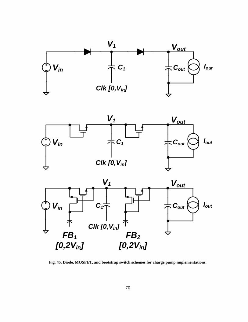
70
Fig. 45. Diode, MOSFET, and bootstrap switch schemes for charge pump implementations.
C1 Vin
V1
Cout Iout
Vout
Clk [0,Vin]
C1 Vin
V1
Cout Iout
Vout
Clk [0,Vin]
C1 Vin
V1
Cout Iout
Vout
Clk [0,Vin]
FB1
[0,2Vin]
FB2
[0,2Vin]

71
Small-signal AC transfer functions for the charge pumps are required for proper
regulation. Both duty cycle and switching frequency dependent control variable analysis
can be performed. Although the analysis presented in [60] is for a LC based switching
converter, its application to other topologies is equally valid as it is a derivation of the
classical approach of state-space averaging [61]. From Fig. 46, the transfer function is
obtained by solving for the time domain transient response in both the charging and
discharging phases taking into account the on-resistances of the switches. From both
charging and discharging equations, an averaged model is obtained:
𝐶𝑜𝑢𝑡
𝑑Vout
𝑑𝑡= (−
𝑉𝑜𝑢𝑡
𝑅𝑜𝑢𝑡) (Ton Fsw)
+ (𝑉𝑖𝑛 + 𝑉1 − 𝑉𝑜𝑢𝑡
𝑅𝑜𝑛−
𝑉𝑜𝑢𝑡
𝑅𝑜𝑢𝑡) (Toff Fsw)
(58)
For duty cycle control, (58) can be made to match as the control variable:
𝐶𝑜𝑢𝑡
𝑑Vout
𝑑𝑡= (−
𝑉𝑜𝑢𝑡
𝑅𝑜𝑢𝑡) (𝐷1)
+ (𝑉𝑖𝑛 + 𝑉1 − 𝑉𝑜𝑢𝑡
𝑅𝑜𝑛−
𝑉𝑜𝑢𝑡
𝑅𝑜𝑢𝑡) (𝐷2)
(59)
Fig. 46. Single stage switched capacitor converter with associated capacitor voltages.
Φ1
Φ2 Φ1
C1 Vin
V1Φ2
Cout Iout
Vout

72
By assuming a 50% duty cycle, i.e. 𝜙1 = 𝜙2 (𝐷1 = 𝐷2), the DC solution is
obtained from the steady-state DC equations for frequency modulation:
𝐶𝑜𝑢𝑡
𝑑(𝑉𝑜𝑢𝑡 + 𝑣𝑜𝑢𝑡)
𝑑𝑡= 0
= (−𝑉𝑜𝑢𝑡 + 𝑣𝑜𝑢𝑡
𝑅𝑜𝑢𝑡) (𝑇𝑜𝑛(𝐹𝑠𝑤 + 𝑓𝑠𝑤))
+ (𝑉𝑖𝑛 + (𝑉1 + 𝑣1) − (𝑉𝑜𝑢𝑡 + 𝑣𝑜𝑢𝑡)
𝑅𝑜𝑛
−𝑉𝑜𝑢𝑡 + 𝑣𝑜𝑢𝑡
𝑅𝑜𝑢𝑡) (𝑇𝑜𝑓𝑓 (𝐹𝑠𝑤 + 𝑓𝑠𝑤))
(60)
As well as duty cycle modulation:
𝐶𝑜𝑢𝑡
𝑑(𝑉𝑜𝑢𝑡 + 𝑣𝑜𝑢𝑡)
𝑑𝑡= 0
= (−𝑉𝑜𝑢𝑡 + 𝑣𝑜𝑢𝑡
𝑅𝑜𝑢𝑡) (𝐷 + )
+ (𝑉𝑖𝑛 + (𝑉1 + 𝑣1) − (𝑉𝑜𝑢𝑡 + 𝑣𝑜𝑢𝑡)
𝑅𝑜𝑛
−𝑉𝑜𝑢𝑡 + 𝑣𝑜𝑢𝑡
𝑅𝑜𝑢𝑡) (𝐷 + )
(61)
Eliminating both DC and nonlinear terms (second order effects), as well as
setting the input voltage to AC ground greatly simplifies analysis and the acquisition of
the effect of both the switching frequency and duty cycle on the control-to-output
voltage transfer function after including the effect of the oscillator linear gain.

73
𝐺𝑣𝑑(𝑠) =
𝑣𝑜𝑢𝑡(𝑠)
𝑑(𝑠)|
𝑖𝑛=0
=−2𝑉𝑜𝑢𝑡𝑅𝑜𝑛
𝑠(𝐶𝑜𝑢𝑡𝑅𝑜𝑢𝑡𝑅𝑜𝑛) + 𝐷(𝑅𝑜𝑢𝑡)
(62)
𝐺𝑣𝑐(𝑠) =𝑣𝑜𝑢𝑡(𝑠)
𝑣𝑐(𝑠)|
𝑖𝑛=0
=−𝑉𝑜𝑢𝑡𝑅𝑜𝑛 ∙ 𝐾𝑉𝐶𝑂
𝑠(𝐶𝑜𝑢𝑡𝑅𝑜𝑢𝑡𝑅𝑜𝑛) + (𝑅𝑜𝑢𝑡)
(63)
Switched capacitor control loop for pulse width modulation
Following the same control loop shown in Fig. 40, the same modulation methods
are available for the switched capacitor regulator. In order for the implementation of a
PWM control scheme a charging profile is implemented by varying the duty cycle of one
of the phase switches 𝜙1,2. Fig. 47 shows how the secondary switch for the 𝜙1 cycle
modulates the amount of current being pulled from the input source; hence, limiting the
charge being transferred from the input source to the output load.
While modifying the duty cycle of the charge being dumped into 𝐶1 allows for a
degree of control, it is limited to a maximum duty cycle of 50% [62]. Any increase in
duty cycle for 𝜙1 beyond 50% negatively affects the charge delivering capability of the
system as not unbalanced charge transfer takes place in the converter, further
complicating linearizing dynamics.

74
Fig. 47. Charge pump PWM implementation.
Φ2 C1
V1
Φ2
VoutVin
Φ1
C1
V1 VoutVin
Icharge
Φ1PWM
Φ1
Φ1PWM
Φ2
10% to 50%

75
If the requirements of the load fall within the regulators capabilities with duty
cycle modulation, the PWM control loop can improve both speed (bandwidth) and
accuracy through the compensation block implemented (Fig. 40). The implementation of
the variable duty cycle block is the same as the one implemented for the inductive
switching regulator (boost converter).
Switched capacitor control loop for pulse frequency modulation
The implementation of variable control frequency in PFM is a commonly used
method in switched capacitive regulators [63-65]. The variable switching frequency
allows for a rapid and accurate voltage regulation mechanism, within the limits of the
output resistance of the regulator, expressed in (23) in Chapter I.
Fig. 48. PFM behavioral model for step-up operation.
Vin
1:N
Rout
Cout Iout
fswitching

76
Fig. 48 represents the PFM behavioral model of the charge pump.
Implementations utilizing bootstrapped switches usually require and additional number
of phases (4 phase non-overlapping clock) to synchronize the turning on-off of the
bootstrap switches prior to the main switches.
Fig. 49 shows the output resistance variations with both number of stages and
switching frequency of the regulator. The output capacitor, 𝐶𝑜𝑢𝑡, is set to 1 μF. As the
plot shows, as the number of stages increases (N) the range over which the output
resistance can vary is reduced. Causing load current variations to be limited to number of
stages if any one particular frequency is to be set.
Fig. 49. Output resistance with variable switching frequency and number of stages.
77
Performance comparison
As both topologies offer their own benefits and disadvantages, a comparison
between both regulator types is presented.
Voltage gain ratio
As presented in both Chapters I and II, the voltage gain capabilities for inductive
and capacitive are performed via the storing and delivering of energy through
complementary cycles. The stored energy is kept in reactive components, allowing for
variable amounts of charge to be deposited.
As the capacitive switching regulator is limited by both frequency and number of
stages, and the applications for which both regulators will be applied for are in energy
harvesting approaches, light-load conditions for both converters will be assumed.
For the inductive regulator the DCM operation is assumed, setting the voltage
gain to be given by (36). And for the capacitive regulator, since the voltage gain is
mainly limited by both load current and number of stages, the ratio is determined by
(56).
Fig. 50 shows how both converters’ voltage gain is varied with duty cycle and
number of stages for the boost converter and charge pump, respectively. Both converters
were set to a switching frequency of 1 MHz, and an input voltage of 1 V. The boost
converter was also set with an input inductance of 100 μH, whereas the charge pump
was set to have 200 pF capacitors per stage.

78
Fig. 50. Voltage conversion ratio for both regulators under light-load conditions.
As can be seen, the main limitation in terms of voltage gain for both topologies
lies in output current demands. As increases in load current will cause the boost
converter to begin operating in CCM/DCM boundary, and the voltage gain drops, the
same occurs with the charge pump as the output current demand increases.
In order to increase M for both regulators with high 𝐼𝑜𝑢𝑡 demands, the boost
converter will need to a lower valued inductor and the charge pump a higher valued
flying capacitor per stage.
Power efficiency
Both regulators possess competitive efficiencies under the light-load regime. The
boost converter’s efficiency is mainly limited to the conduction losses present in the on-
resistance of both switches and input inductor as the light-load specification allows for
smaller MOSFET switches to be implemented, reducing the overall switching losses
(12⁄ ∙ 𝐶𝑔𝑎𝑡𝑒 ∙ 𝑉𝑑𝑟𝑖𝑣𝑒
2 ∙ 𝑓𝑠𝑤).
Boost Converter
in DCMCharge Pump

79
The efficiency expression is then given by:
𝜂𝐵𝑜𝑜𝑠𝑡 =𝑃𝑖𝑛𝑝𝑢𝑡 − (𝑃𝑁𝑀𝑂𝑆 + 𝑃𝑃𝑀𝑂𝑆 + 𝑃𝑖𝑛𝑑𝑢𝑐𝑡𝑜𝑟)
𝑃𝑖𝑛𝑝𝑢𝑡
(64)
where
𝑃𝑁𝑀𝑂𝑆 = 𝑅𝑁𝑀𝑂𝑆 ∙ 𝐷1 ∙ (𝐼𝑜𝑢𝑡
1 − 𝐷1)
2
(65)
𝑃𝑃𝑀𝑂𝑆 = 𝑅𝑃𝑀𝑂𝑆 ∙ 𝐷2 ∙ (𝐼𝑜𝑢𝑡
1 − 𝐷2)
2
(66)
𝑃𝑖𝑛𝑑𝑢𝑐𝑡𝑜𝑟 = 𝑅𝐿𝑖𝑛 ∙ (𝐼𝑜𝑢𝑡
1 − 𝐷1)
2
(67)
Assuming low valued DC resistance for the inductor, the switches become the
main efficiency limitation for DCM boost converter topologies.
Fig. 51. Power efficiency for boost converter with variable duty cycle and increasing output load
current in DCM.
Iout in
cre
ase
s
Iout = 200 µA
Iout = 10 µA

80
For the charge pump’s efficiency several assumptions can be made. Whenever
diodes or MOSFET connected diodes are replaced by active switching, the main loss
factor in charge pumps become the parasitic capacitance of the used flying capacitors
[66]. This leaves the following expression for overall efficiency of the converter:
𝜂𝑐ℎ𝑎𝑟𝑔𝑒 =
𝑉𝑖𝑛 ∙ 𝐼𝑜𝑢𝑡 ∙ (𝑁 + 1) −𝑁 𝐼𝑜𝑢𝑡
2
𝑓𝑠𝑤 ∙ 𝐶𝑠𝑡𝑎𝑔𝑒
𝑉𝑖𝑛 ∙ 𝐼𝑜𝑢𝑡 ∙ (𝑁 + 1) + 𝛼 ∙ 𝐶𝑠𝑡𝑎𝑔𝑒 ∙ 𝑓𝑠𝑤 ∙ 𝑉𝑖𝑛2 (68)
where 𝛼 is the parasitic to main capacitance value ratio for each stage flying capacitors
[67].
Fig. 52. Power efficiency for charge pump with variable load current and increasing number of
stages.
N=1
N=4
N=7
N=10

81
Both regulator topologies offer benefits at low and high current load demands
and integration capability; where the boost converter displays overall better efficiency,
but limited integration options.
Integration
It is in this aspect where the capacitive switching regulator allows for a fully
monolithic approach. Current technology processes allow for high capacitance density
per area (F/μm2) where flying capacitors above 150 pF are achievable [42, 68].
Nonetheless, as expressed in (68), the efficiency is affected by the capacitance ratio of
the parasitic capacitance to implemented capacitor (𝛼 = 𝐶𝑝𝑎𝑟𝑎𝑠𝑖𝑡𝑖𝑐/𝐶𝑠𝑡𝑎𝑔𝑒). Fig. 53
shows a cross section of the implementation of Metal-Insulator-Metal (MIM) capacitor.
Fig. 53. Parasitic capacitance for on-chip capacitors implemented for charge pumps.
Metal Y
Metal X
InC InCDielectric
substrate
Cstage
CparasiticDielectric

82
The main capacitor is formed with metals Y and X for 𝐶𝑠𝑡𝑎𝑔𝑒; the issue arises
with the 𝐶𝑝𝑎𝑟𝑎𝑠𝑖𝑡𝑖𝑐 element from Metal X to the substrate. The more distance between
the bottom plates (Metal X) to the substrate the lower the value for parasitic
capacitances.
Other capacitor creation methods for on-chip processes have also been explored:
on-chip trench capacitors [69] or metal finger capacitors [70]. These implementations
are limited to special process technologies which are able to offer such types of
capacitors.
For the boost converter the main focus is to minimize the off-chip inductance by
integrating the magnetic component on-chip. Although efforts to present integrated
inductors through top metal coils on-chip of use of bond-wire for inductor purposes [71-
74], they are limited to low quality factor designs for light-load demands and require
high switching frequencies to take full advantage of the storing capabilities of the
inductor.
Trade-offs
As has been shown throughout this chapter, both regulator topologies offer a
voltage regulation capability to the output. Where the switched capacitor regulator offers
higher integration capability, the switched inductive regulator possesses inherently
higher efficiency and higher power delivery capabilities. TABLE 5 shows a comparative
view of both regulator topologies.

83
TABLE 5. Comparison table for both regulator topologies presented.
Switched Capacitive Regulator
Switched Inductive Regulator
Topology Complexity
High (for multistage regulators)
Low
Control Implementation Medium Medium
Footprint Small
Large (due to off chip inductor)
Efficiency Low (At high current demands)
High
Output current Low High
Fig. 54. Input-output voltage characteristic of Linear regulator.
OffDropout Region
Linear Region
Vin
Vout
0 Headroom
Max drive
Low loop gain
V
V

84
Linear regulators
As mentioned in Chapter I, linear regulators achieve DC-DC voltage conversion
by dissipating excess power into a resistive element; essentially making these regulators
resistive dividers. Utilizing active devices as the dissipating element, the output voltage
is set through a control loop which varies the active devices on resistance. A linear
regulator has three operational regions: off, dropout region, and linear operation, Fig. 54
illustrates presents the regions and their typical characteristics.
It is during the linear region where the regulator operates and fixes the output
voltage with a finite and non-zero loop gain. Decreasing 𝑉𝑖𝑛 causes the pass device to
enter its linear (MOSFET) or saturation (BJT) region in which the gain of the active pass
device is low. The regulator still operates, although with minimum loop gain, causing
DC errors in the regulated value of 𝑉𝑜𝑢𝑡.
Decreasing 𝑉𝑖𝑛 even further causes the system to enter the dropout region, which
is where the regulator operates at its driving limit. The pass device still supplies as much
current in order to keep 𝑉𝑜𝑢𝑡 regulated. Additional decreases in 𝑉𝑖𝑛 forces the regulator
to be unable to maintain regulation at all.
Low dropout regulators
Low dropout regulators (LDO) are made up of a control loop which senses the
output voltage in order to maintain the output voltage constant, within a specific
tolerance level. They appear in two different topologies: source-follower/common-
collector and common-source/common-emitter.

85
Fig. 55. Common-collector LDO topology with NPN active device.
Fig. 55 illustrated a block level composition of a common-collector LDO
topology with NPN transistor as the pass device. This type of regulator requires base
driving voltages in excess of the input voltage in order to fully drive the device for high
current demands. The common-collector topologies are present in low-voltage
applications [75], but require the implementation of charge pump converters to deliver
the appropriate base driver levels. The main common-collector topology efficiency
under ideal conditions yields:
𝜂𝐿𝐷𝑂 =
𝑉𝑖𝑛 − 𝑉𝑜𝑢𝑡
𝑉𝑖𝑛=
𝑉𝑑𝑟𝑜𝑝𝑜𝑢𝑡
𝑉𝑖𝑛= 1 −
𝑉𝑜𝑢𝑡
𝑉𝑖𝑛
(69)
It is the common-source/common-emitter voltage regulator topology that
overcomes the high gate voltage requirements from the source-follower regulator; by
setting the 𝑉𝐷𝑆/𝑉𝐶𝐸 voltage of the active device as the main parameter that limits the
RLoad
Vout
Pass Transistor
Vin
RL1
RL2
Vref
Vcc>Vin

86
regulator operation. In the MOSFET instance, it is the dropout voltage (𝑉𝐷𝑆𝐴𝑇) which
limits the output current and size of the pass device.
Fig. 56. Common-source LDO topology with NMOS active device.
Fig. 56 shows the common-source topology of the LDO. The main difference
between the PNP and PMOS implementation of this topology is the use of much reduced
quiescent current by the PMOS, which in turn increases the drive portability, battery
operation, and overall reduced power consumption [76].
Principles
The LDO is fully comprised of a voltage reference, error amplifier, a pass
transistor, and a feedback network (Fig. 55 and Fig. 56). The feedback network senses
the output voltage, delivering a fraction of the output voltage the error amplifier. The
RLoad
Vout
Pass Transistor
Vin
RL1
RL2
Vref

87
error amplifier then compares and generates an error signal that drives the pass device
and regulates the output voltage.
The output voltage of the regulator is set through both the reference voltage and
ratio of feedback resistors. This is determined for an ideal error amplifier as:
𝑉𝑜𝑢𝑡 = (1 +
𝑅𝐿1
𝑅𝐿2) 𝑉𝑟𝑒𝑓
(70)
A second critical aspect in the regulator design is the pass device dimensions.
The dimensions set the maximum amount of current the regulator can deliver to the load.
The pass device dimensions are usually large in order to deliver enough current for the
application:
𝑊
𝐿 𝑃𝐴𝑆𝑆=
2 ∙ 𝐼𝑃𝑎𝑠𝑠
𝜇𝑋𝐶𝑂𝑋(𝑉𝐺𝑆 − 𝑉𝑇)2
(71)
where 𝐼𝑃𝑎𝑠𝑠 is the current through the pass device, 𝜇𝑥 the mobility of electrons/holes,
𝐶𝑂𝑋 the oxide capacitance, 𝑉𝐺𝑆 the gate to source voltage difference and 𝑉𝑇 the threshold
voltage.
The main downside of having a large pass device is the associated parasitic
capacitances. These parasitic capacitances cause an unwanted time delay whenever load
event occurs, charging-discharging these capacitances requires additional charge to fully
enhance the depletion channel generated by the pass device.

88
Each pass device topology has their associated stability requirements. While the
source-follower/common-collector topology possesses an inherently stable response, due
to its low output impedance; only two poles are within the bandwidth of interest: the
dominant 𝑃1 generated by the error amplifier driving stage’s output impedance (𝜔𝑝1 =
1/(𝑅𝑜𝑢𝑡𝐶𝑝𝑎𝑠𝑠) ), and the secondary pole 𝑃2 generated with the load impedance and
emitter/source impedance. Fig. 57 shows the typical small-signal response for this
topology.
Fig. 57. Small-signal pole locations for source-follower topology.
For the common-source/collector topology stability is a prime concern as the output
capacitor and high output impedance of the pass device set the dominant pole of the
regulator at the output node.
RLoad
Vout
Pass Transistor
Vin
RL1
RL2
Vref
Ga
in (
dB
)
Frequency (Hz)P1 P2
P1
P2
Vcc>Vin
CLoad

89
This causes the dominant pole 𝑃1 (𝜔𝑝1 = 1/(𝑅𝑜𝑢𝑡𝐶𝑝𝑎𝑠𝑠)) to come in close
proximity to the pole located at the output of the error amplifier 𝑃2 (𝜔𝑝2 = 1/
( 𝑅𝐿𝑜𝑎𝑑𝐶𝐿𝑜𝑎𝑑)). This requires external or internal compensation of the regulator in order
to correctly operate. Fig. 58 shows the typical small-signal response for this topology.
Different approaches have been sought out to stabilize this topology ranging
from taking advantage of the load capacitor’s ESR, external or internal creation of small-
signal zero responses, or eliminating the external capacitor altogether through multiple
loop configuration to ensure stability over wide current and capacitance loads [77, 78].
Fig. 58. Small-signal pole locations for common-source topology.
Digital LDO approach
So far the presented solutions have shown the behavior of LDO regulators with
analog approaches. The same implementation can be taken into the digital domain and
perform the regulation qualities through fully digital means.
RLoad
Vout
Pass Transistor
Vin
RL1
RL2
Vref
Ga
in (
dB
)
Frequency (Hz)P1 P2
P2
P1
CLoad

90
Going back to the principle of operation of a linear regulator, we can see that the
main purpose of the system is akin to a resistive divider. In an analog LDO, this is
performed by modifying an active device’s transconductance to achieve the required
output voltage over load current demands. Stability, power consumption, and speed are a
major set of concerns for analog LDOs. The same regulating properties can be achieved
by digital means as well. As the dropout voltage for a device is dependent on pass device
dimensions, a fragmented pass device into multiple single units can also mimic the effect
of an analog voltage driving a single large device, this is better shown as follows:
𝐼𝐷𝑖 =
𝜇𝐶𝑜𝑥
2(
𝑊
𝐿)
𝑖(𝑉𝑔𝑠 − 𝑉𝑡ℎ)
2
(72)
It is through the (𝑊
𝐿)
𝑖 ratio that the current load demand is met and voltage
regulation achieved. Fig. 59 shows an overall view of a Digital LDO implementation
with multiple pass devices making up the single pass device from the analog LDO
approach.

91
Fig. 59. Digital LDO implementation with PMOS array for pass devices.
The means by which the digital LDO approach is achieved is through a digital
control loop implemented in the voltage domain. Fig. 60 shows a simple implementation
for a digital LDO controller in voltage domain. The controller is comprised of a
comparator, up/down counter, and N-bit decoder [79]. The decoder number of bits is
dependent on the number of fragmented pass device units. As a load current demand
occurs, the output voltage would fall due to the insufficient driving current from the pass
device. This would make the comparator trigger the event and increase the number of
pass devices turned on, increasing the driving current to the load. The opposite effect
would occur (decrease number of units in pass device) whenever less current is required.
PMOS Array
ILoad
Digital Regulation
Array control
Vout
Vin
Regulation Loop
Voltage
Sensing
Pass Device
fragmented
into N devices

92
Fig. 60. Voltage domain controller for digital LDO implementation.
This topology also has an additional clocked signal to synchronize the entire
operation between the counter and decoder. This makes the clock frequency, 𝑓𝑐𝑙𝑘, the
main performance variable to optimize the system performance. Low 𝑓𝑐𝑙𝑘 allows for a
much improved efficiency, reducing dynamic power consumption, but causing higher
load regulation errors. This is caused by the reaction time between the comparator and
counter to load current events. Higher 𝑓𝑐𝑙𝑘 reduces the load regulation error, but
increases the amount of power consumed by the system. A careful trade-off between
load error and system efficiency exist in digital LDO implementations.
Iload
Load step
Vout
Pass Device fragmented
into N devices
Vin
Counter
Decoder
N-bit
Vref
Increasing number of
devices in array
Decreasing number of
devices in array fclk

93
Performance comparison and state-of-the-art
Digital LDO implementations were sought after as a solution to power
management in deep submicron technology; processes where dynamic power
consumption were minimal due to small size devices. Although not as robust as an
analog LDO implementation, the digital counterpart offers lower power consumption,
and almost synthesizable approach to design.
TABLE 6 presents current state-of-the-art design implementing digital LDO
systems for voltage regulation. Due to the switching nature of the digital LDO (adding
and subtracting pass device units), Power Supply Rejection (PSR) is not a parameter
included in most designs.

94
TABLE 6. Comparison table with state-of-the-art digital LDO implementations.
[79] [80] [81] [82]
Technology 40 nm 90 nm 65 nm 40 nm
Minimum Vin 0.9 V 2.4 V 0.5 V 1.34 V
Vout 1 V 1.2 V 0.45 V 1.2 V
Minimum Dropout
voltage 100 mV 1.2 V 50 mV 1.4 V
Output Capacitor None None None None
Current
Consumption 50 nA 25.7 mA 2.7 μA 130-100 nA
Active area 0.08 mm2 0.03 mm
2 0.042 mm
2 0.057 mm
2
Efficiency 99.90% 97.50% 98.70% 96-99.9 %
As technology continues to decrease in size and multiple voltage domains will be
required on-chip, smaller and more power efficient voltage regulators will be required.
Digital LDOs offer a solution for this dilemma by offering a quick and robust regulator
with minimum variable components. Combinations of types of converters can be used to
operate together and deliver multiple voltage domains for a full System on Chip (SoC)
operation.

95
CHAPTER III
A BOOST CONVERTER WITH DYNAMIC INPUT IMPEDANCE MATCHING FOR
DC ENERGY HARVESTING SOURCES*
Introduction
One of the most critical aspects in wireless sensor nodes is the limited available
energy on the system from onboard batteries. As systems continue to increase in power
density, battery life lags behind these needs. One possible solution lies in energy
harvesting (EH), which presents itself as a means of increasing battery life and
sustaining up-time for the wireless sensor node to a theoretical never-ending power
supply [18, 83-87]. Energy processing circuits designed to work at ultra-low power
levels have been developed for a variety of energy sources such as vibrational, solar,
radio frequency, and thermal. A thermoelectric generator (TEG) delivers a voltage, VTEG,
that is proportional to the difference of the temperatures applied to each side of the
device. The resulting voltage output magnitude varies over a wide range as a function of
the temperature gradients applied.
Previous reports on EH power management units (PMU) for TEGs [17, 20, 88-
90] have focused on harvesting energy from single TEG units utilizing boost converters
(BC). Although these reported systems have shown good efficiency for single units, no
efforts have been made to utilize TEGs placed in a multiple array fashion. A recent
* Reprinted with permission from “A Boost Converter With Dynamic Input Impedance Matching For DC
Energy Harvesting Sources” by S. Carreon-Bautista, A. Eladawy, A. Mohieldin, and E. Sanchez-Sinencio,
2014. IEEE Trans. On Industrial Electronics, vol. 61, no. 10, pp. 5345-5353, Oct. 2014, © 2014 IEEE

96
Fig. 61. Multi-array TEG grid parallel (top), series (bottom) configuration.
publication [86] has also shown how sub-micron technologies allow for lower startup
voltages and improved efficiency; however, it does not deal with on-chip built-in
impedance matching schemes.
If multiple TEG units are placed in an array fashion, a higher power density
becomes available to the load system. The control scheme required to handle the
dynamic connection for the TEG array, implemented through a state machine, would be
capable of changing the manner in which individual TEG units are connected within the
array. This reconfiguration would be based on the available temperature gradients. The
state-machine implementation is not within the scope of the present work. Fig. 61

97
illustrates two possible ways in which the TEG units would be interconnecting their
terminals to maximize temperature gradients power. For example, for low temperature
gradients, the TEG units would be placed in series as shown in the bottom configuration
of Fig. 61. Resulting in an equivalent 𝑉𝑇𝐸𝐺 with an internal resistance 𝑅𝑇𝐸𝐺 = 𝑅 ∙ 𝑛,
where R is the internal resistance of one TEG unit, and 𝑛 is the number of units. To
maximize efficiency, the input impedance of the PMU used for thermal EH of such a
multi-array TEG must change dynamically along with the array. This internal resistance
𝑅𝑇𝐸𝐺 will vary dynamically depending on the temperature gradient. If the internal
resistance is not matched by the PMU, maximum power transfer will not occur. Wide
varying impedance variations, due to TEG grid reconfiguration, are a key issue not
addressed by previous EH solutions in literature.
The PMU presented in this dissertation is a step-up switching converter system,
capable of tracking these impedance matching changes and delivering maximum power
at all times. The maximum power point tracking (MPPT) system is proposed and applied
to a BC operating in a discontinuous conduction mode (DCM) with pulse frequency
modulation (PFM). Furthermore, a pseudo-zero current switching (P-ZCS) scheme is
also implemented to achieve a high efficiency. Fig. 62 illustrates the topology of a BC
implementing independent controls for the NMOS and PMOS switch controls (𝑉𝐶𝑁 and
𝑉𝐶𝑃) through their respective duty cycles (𝐷𝑁𝑀𝑂𝑆 and 𝐷𝑃𝑀𝑂𝑆). Based on this topology, a
MPPT scheme is proposed having independent control over the two MOS switches.

98
Fig. 62. Schematic of BC with synchronous rectification.
Maximum power point tracking
The critical factor for achieving maximum power transfer from a TEG EH source
is to match the TEG array impedance (𝑹𝑻𝑬𝑮) with the input impedance (𝒁𝒊𝒏) of BC.
Once both impedances are matched the voltage at the input of the BC becomes the TEG
source (𝑽𝑻𝑬𝑮) divided by two. To achieve maximum power point (MPP) state, it is
critical to determine the internal impedance range of the TEG array to know the input
impedance range. For commercially available TEG sources [91-94], it is known that the
internal impedances can range from Ωs to kΩs. From [94], the fixed output electrical
impedance for a single 10 mm2 unit is approximately 300 Ω. Depending on the
connection type for the individual TEG units (parallel, series, or a combination), 𝑹𝑻𝑬𝑮
would not be fixed and would require tuning the input impedance of the switching
converter to fully reach MPP operation.
In [20], 𝒁𝒊𝒏 is approximated as a function of the inductor current charge and
discharge, yielding:

99
𝑍𝑖𝑛 =
𝑉𝑖𝑛
𝐼𝑖𝑛𝑝𝑢𝑡=
2 ∙ 𝐿𝑖𝑛
𝑡𝑁𝑀𝑂𝑆2 ∙ 𝑓𝑠
(1 +𝑡𝑃𝑀𝑂𝑆
𝑡𝑁𝑀𝑂𝑆)
−1
(73)
where 𝑉𝑖𝑛 is the input voltage of the BC, 𝐼𝑖𝑛𝑝𝑢𝑡 is the input current going through the
inductor, 𝐿𝑖𝑛 is the storage inductor for the BC, 𝑓𝑠 is the switching frequency, 𝑡𝑁𝑀𝑂𝑆 and
𝑡𝑃𝑀𝑂𝑆 are the NMOS and PMOS on times, respectively. Both 𝑡𝑁𝑀𝑂𝑆 and 𝑡𝑃𝑀𝑂𝑆 are
related to the duty cycle by 𝑡𝑁𝑀𝑂𝑆,𝑃𝑀𝑂𝑆 = 𝐷𝑁𝑀𝑂𝑆,𝑃𝑀𝑂𝑆 ∙ 𝑇𝑠, where 𝐷𝑁𝑀𝑂𝑆,𝑃𝑀𝑂𝑆 is the
duty cycle for the NMOS and PMOS switches, respectively, and 𝑇𝑠 is the period.
This research’s design was structured to directly work with a small grid application to
prove the capabilities of matching variable impedances. The proof of concept prototype
involves the system design for a 3x3 TEG grid composed of units with variable
connections in parallel and series.
One of many possible applications for the system lies in wearable medical
applications where a minimum temperature difference is obtained from the skin-
environment interface. With temperature differences ranging from 0.4° C to 2° C, the
TEG grid would be reconfigured to deliver the highest amount of power directly into the
BC. TABLE 7 shows the design specifications for the converter presented in this
dissertation. From the reconfigurable TEG grid design, the design presents two different
impedance extreme scenarios: a 2.7 kΩ 𝑅𝑇𝐸𝐺 from the TEG grid where the units are all
connected in series and a 33.33 Ω 𝑅𝑇𝐸𝐺 where the units are all connected in parallel.

100
TABLE 7. Design specification for converter.
SPECIFICATION VALUE
𝑽𝒊𝒏 20 mV→150 mV
𝑽𝒐𝒖𝒕 1.8 V→2.5 V
Maximum efficiency >60%
Impedance Matching
Range 33.33Ω→2.7kΩ
Quiescent Power
Consumption <1 𝜇𝑊
Proposed dynamic matching for boost converter
For the present design the DCM mode of operation was selected for the system
design in order to keep power consumption to a minimum due to the low power density
of EH sources. PFM modulation was also implemented in order to reduce losses at light
loads and improve efficiency [55].
A relationship between (73) and [55] can be made and (73) is rewritten as
follows:
𝑍𝑖𝑛 ≈
𝑅𝑒 ∙ (𝑀 − 1)
𝑀
(74)
where 𝑅𝑒 is defined as the effective impedance seen through the input port of the BC
(𝑉𝑖𝑛) in Fig. 62, and 𝑀 is the conversion gain of the BC.
𝑅𝑒 =
2 ∙ 𝐿𝑖𝑛 ∙ 𝑓𝑠
𝐷𝑁𝑀𝑂𝑆2
(75)
𝑀 ≈ 1 +
𝑡𝑁𝑀𝑂𝑆
𝑡𝑃𝑀𝑂𝑆= 1 +
𝐷𝑁𝑀𝑂𝑆
𝐷𝑃𝑀𝑂𝑆
(76)

101
Assuming that 𝑡𝑁𝑀𝑂𝑆 ≫ 𝑡𝑃𝑀𝑂𝑆, (74) effectively becomes equal to (75). For the
PFM scheme used in the proposed system, a constant duty cycle of 50% is established
for the NMOS switch. This decision to keep 𝐷𝑁𝑀𝑂𝑆 fixed was due to the quadratic nature
of the relationship between input impedance and the NMOS duty cycle (75). The value
of (75) would change at a much faster rate than when varying the switching frequency.
The issues that arise by this possible implementation are the available resolution with
which the duty cycle of the NMOS would be controlled. Implementing a traditional
PWM scheme would hinder the overall system efficiency, and implementing a digital
PWM would require additional system blocks which could also limit the efficiency of
the converter. Hence, this leaves the values for (75) dependent on 𝑓𝑠 and 𝐿𝑖𝑛 of the
converter. Fig. 63shows the effect of varying 𝑓𝑠 along with 𝐿𝑖𝑛 for 𝑍𝑖𝑛.
Fig. 63. Contour plots of input resistance variation with Lin and fs.

102
Selecting an inductor value that is too small may cause a much more stringent
requirement on the system’s 𝑓𝑠 to effectively cover the entire 𝑍𝑖𝑛 variation. Likewise,
setting an inductor value that is too large becomes impractical due to the amount of
inductor resistance (DCR) included as well as size. For the presented design, a fixed on-
time PFM with 50% duty cycle was implemented using a 1mH inductor with a low DCR
of 370 mΩ and small footprint (5.6 mm x 7.1 mm).
From Fig. 63, selecting 𝐿𝑖𝑛 to 1 mH bounds the control range for 𝑓𝑠 for nearly a
decade that is between 4.2 kHz and 337.5 kHz. This frequency range allows for the
implementation of a low power VCO. Depending on the technology, the target
application and range of impedances to match, smaller values for the inductor can be
selected to optimize the design.
Fig. 64 presents the overall block diagram of the proposed MPPT system. The
matching is achieved through the MPPT control via a PFM modulator. By varying 𝑓𝑠 of
the BC through a voltage control oscillator (VCO), 𝑍𝑖𝑛 is varied by 𝑓𝑠 to adjust the input
voltage of the BC and achieve MPPT.
Block diagram for dynamic MPPT
Analogous to a Phase Locked Loop (PLL) which possesses a capture range, the
MPPT scheme possesses a matching range for which it can achieve maximum power
point with a harvesting transducer. The system implemented in Fig. 64 allows the design
to lock and match for abrupt impedance changes because of the ample bandwidth.

103
Fig. 64. Block diagram of proposed MPPT system.
This is performed in a similar fashion in which a PLL locks on to different
channels in a short period. Note that the system present in [90], assuming a single
capacitor filter (with limited bandwidth), would not be able to “lock” to the sudden and
large impedance variations under a rapid conditions that would appear due to the TEG
rearrangement process due to its limited stability parameters for the matching loop.
For the linear model of the MPPT system, the open circuit voltage (Voc), that
arises from the open circuit voltage of the TEG grid, will be used as the input variable.
The block diagram in Fig. 65 shows the components of the MPPT system implemented
and Fig. 66 shows the small signal linearized equivalency used to track its dynamic
behavior.
The source 𝑉𝑜𝑐 is divided by 2 and compared to the input voltage (𝑉𝑖𝑛) seen by
the BC. From the linearized model of the MPPT implementation in Fig. 66, the open
loop transfer function becomes:

104
𝑇𝐹𝑂𝐿 = 𝐾𝑃 ∙ 𝐾𝐶𝑃 ∙ 𝐹(𝑠) ∙ 𝐻𝑐−𝑖𝑛(𝑠) (77)
where 𝐾𝑝 is the comparator gain, 𝐾𝐶𝑃 is the gain due to the charge pump, 𝐹(𝑠) is the
transfer function for the filter, and 𝐻𝑐−𝑖𝑛(𝑠) is the BC control-to-input voltage transfer
function.
Fig. 65. Block diagram for MPPT implementation.
To minimize power consumption, the charge pump quiescent power is reduced
by limiting the bias current; this leaves the filter as the one factor in the design with
allowance for performance improvement.

105
The filter allows for an improved phase margin as well as extended bandwidth
for the system. Depending on the implementation, this can permit faster locking time and
minimize ringing due to sudden impedance changes. It is the implementation of the filter
within the MPPT control loop which allows for the broad impedance matching.
To obtain the effect that the input voltage has in relation to the control signal 𝑉𝐶,
the system behavior is approximated by linearizing the BC around an operating point.
Fig. 66. Small-signal linear model of MPPT block.
∑

106
Fig. 67. Control-to-input voltage transfer function model of boost converter.
Assuming the output voltage reaches a steady state DC voltage via the regulating
mechanisms (P-ZCS and comparator); both the output and input voltage sources are
assumed to behave as AC grounds in small signal as shown in Fig. 7. In [55], a small
signal model for the BC operating under a PFM scheme was presented. Fig. 67
represents the aforementioned small signal model, where the parameters 𝑗𝑥, 𝑟𝑥, and 𝑔𝑥
are obtained via three dimensional Taylor series expansions of the average input and
output voltages and duty cycle [95]. The variable 𝑉𝑐(𝑠), seen in Fig. 67, is the VCO
control voltage coming in from the filter block (Fig. 65).
Thus the control-to-input voltage transfer function 𝐻𝑐−𝑖𝑛(𝑠) can be obtained.
Following the small signal model from [55], the PFM control-to-input voltage transfer
Switch Small-Signal Model
for PFM
Cin r1 j1·Vc(s)
v1
Vout
L1
Lin
Vin
j2·Vc(s)
v2
r2
g1·v2
g2·v1
Iinput
RTEG

107
function is acquired, which includes the effects of 𝑓𝑠 as well as the gain of the VCO
block.
𝐻𝑐−𝑖𝑛(𝑠) =𝑉𝑖𝑛(𝑠)
𝑉𝑐(𝑠)=
𝑗1𝑟1
𝐿𝑖𝑛𝐶𝑖𝑛
𝑠2 + 2𝜉𝜔𝑜𝑠 + 𝜔𝑜2
(78)
where
𝜔𝑜 = √𝑅𝑇𝐸𝐺 + 𝑟1
𝐿𝑖𝑛𝐶𝑖𝑛𝑅𝑇𝐸𝐺
𝜉 =(𝐿𝑖𝑛 + 𝐶𝑖𝑛𝑅𝑇𝐸𝐺𝑟1)
2√(𝐶𝑖𝑛𝐿𝑖𝑛𝑅𝑇𝐸𝐺)(𝑅𝑇𝐸𝐺 + 𝑟1)
As can be seen from (78), the analytical transfer function for the control-to-input
voltage in PFM would closely resemble its Pulse Width Modulation (PWM) counterpart
[95]. The disparity lies in the magnitude of the transfer function due to the addition of
the VCO gain (𝐾𝑣𝑐𝑜) and 𝑓𝑠 terms in the 𝑗1 small signal parameter.
For the presented design, a VCO with 𝐾𝑉𝐶𝑂 of 550 𝑘𝐻𝑧/𝑉 was used; this VCO
gain selection is justified in Section IV. Fig. 68 shows the Bode plot comparison
between (78) and the simulated one when 𝑓𝑠 is set at 100 kHz. Agreement between both
analytical and simulated results is shown with 9% error in magnitude at DC; the gain
mismatch for the magnitude is from the VCO gain and nonlinearity of the block.
As in PLLs, different compensation schemes can be implemented to extend
bandwidth and minimize ringing. Using the initial assumption that the filter 𝐹(𝑠) is
comprised only of a single storage capacitor given by 𝐶𝑓 [90], taking (78) and expanding
from (77) yields the open loop transfer function:

108
𝑇𝐹𝑂𝐿 =
𝐾𝑝 ∙ 𝐾𝐶𝑃
𝑠𝐶𝑓∙ 𝐻𝑐−𝑖𝑛(𝑠)𝑃𝐹𝑀
(79)
This open loop transfer function allows for an insight on the parameters affecting
fast changing series impedances and the requirements to achieve MPPT. Assuming a
value of 𝑉𝑖𝑛,𝐷𝐶 of 100 mV, 1 μF for 𝐶𝑓, a 𝐾𝑃 ≈ 90dB, and 𝐾𝐶𝑃 can be approximated as
the static current consumed by the charge pump [96] or 0.5 μA in Fig. 65.
The frequency response for the entire open loop system for the mid-range value
of 𝑅𝑇𝐸𝐺 = 1.366 𝑘Ω; results in a phase margin (PM) of 16° and unity gain frequency of
82.4 Hz. This presents a conditionally stable system but with an ample amount of
ringing and a limited bandwidth that will react slowly to drastic impedance changes from
the TEG grid.
Fig. 68. Analytical (5) vs. simulated results: (left) magnitude, (right) phase.
100
101
102
103
104
-100
-90
-80
-70
-60
-50
-40
-30
-20
Frequency (Hz)
Magnitude (
dB
)
|Hc-in
()|
Simulated
Analytical
100
101
102
103
104
-140
-120
-100
-80
-60
-40
-20
0
Frequency (Hz)
Phase (
degre
es)
Hc-in
()
Simulated
Analytical

109
This limited range approach would not be able to cope with the sharp impedance
variations which would take place with the TEG array reconfiguration. Implementing a
different filter configuration would allow for a much faster, and overall stable response
from the system (increased bandwidth), while maintaining good PM.
A type II filter [54], illustrated as 𝐹(𝑠) in Fig. 65, was implemented to obtain a
unity gain frequency was driven to 2.24 kHz and a PM of 89.2°. This implemented filter
allows for the system to be stable under the abrupt impedance changes presented by the
TEG grid. Section IV further elaborates on the implementation.
Fig. 69. Inductor current behavior for P-ZCS scheme.
ILin
PMOS
Control
VSW
Counter
Control Down Up
DPMOS
DNMOS
t1 t2 t3 t4
Detected
voltage surge

110
Algorithm for pseudo zero current switching
In order to minimize component stress and increase efficiency, a zero current
switching (ZCS) technique is employed. The P-ZCS is implemented to minimize the
inductor current losses through the PMOS switch. The P-ZCS is performed via a skewed
voltage peak detector in the 𝑉𝑆𝑊 node (Fig. 62).
Fig. 69 shows the overall current and voltages associated with the P-ZCS
algorithm. At time interval t1-t2, considering the inductor is completely discharged when
the PMOS switch is turned off, no voltage peaking should be discernible at the VSW node
since the inductor current reverses direction. As noted by [88], this drains the parasitic
capacitors associated with the VSW node before turning on the drain-bulk diode of the
NMOS switch.
Fig. 70. Pseudo-ZCS control algorithm.
VSW detection Counter
Delay
ArrayDNMOS
VSW
8DPMOS
8:1
MUX
Control
Delay
Input
3
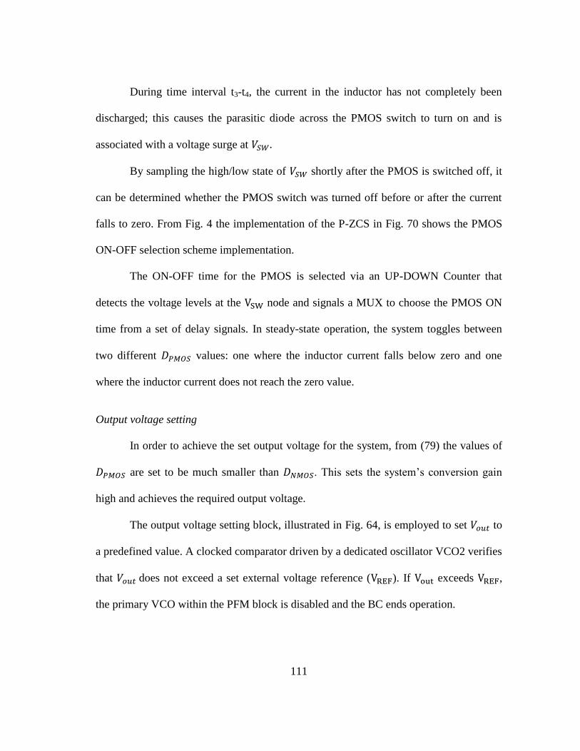
111
During time interval t3-t4, the current in the inductor has not completely been
discharged; this causes the parasitic diode across the PMOS switch to turn on and is
associated with a voltage surge at 𝑉𝑆𝑊.
By sampling the high/low state of 𝑉𝑆𝑊 shortly after the PMOS is switched off, it
can be determined whether the PMOS switch was turned off before or after the current
falls to zero. From Fig. 4 the implementation of the P-ZCS in Fig. 70 shows the PMOS
ON-OFF selection scheme implementation.
The ON-OFF time for the PMOS is selected via an UP-DOWN Counter that
detects the voltage levels at the VSW node and signals a MUX to choose the PMOS ON
time from a set of delay signals. In steady-state operation, the system toggles between
two different 𝐷𝑃𝑀𝑂𝑆 values: one where the inductor current falls below zero and one
where the inductor current does not reach the zero value.
Output voltage setting
In order to achieve the set output voltage for the system, from (79) the values of
𝐷𝑃𝑀𝑂𝑆 are set to be much smaller than 𝐷𝑁𝑀𝑂𝑆. This sets the system’s conversion gain
high and achieves the required output voltage.
The output voltage setting block, illustrated in Fig. 64, is employed to set 𝑉𝑜𝑢𝑡 to
a predefined value. A clocked comparator driven by a dedicated oscillator VCO2 verifies
that 𝑉𝑜𝑢𝑡 does not exceed a set external voltage reference (VREF). If Vout exceeds VREF,
the primary VCO within the PFM block is disabled and the BC ends operation.

112
Once the system reaches an operational steady state, 𝑉𝑜𝑢𝑡 can be set as the internal
supply source for the system (𝑉𝐷𝐷). It should be noted that VCO2’s clock signal, for the
comparators in the system, is never disengaged. This allows continuous monitoring of
input and output voltages. As VCO2 maintains operation even when 𝑉𝑜𝑢𝑡 exceeds 𝑉𝑅𝐸𝐹,
on average 𝑉𝑜𝑢𝑡 is never more than a few cycles of VCO2 over 𝑉𝑅𝐸𝐹. Furthermore, 𝐶𝑖𝑛
and 𝐶𝑜𝑢𝑡 are both fairly large valued (10μF); these capacitors maintain both the input
and output voltage comparatively constant when compared to both the switching
frequencies of VCO and VCO2.
Typically EH power management systems disengage the source after the desired
output voltage is reached [17, 86, 89, 97]. However, different configurations can be
implemented with the BC in order to minimize the time the system is disabled: i) A more
demanding variable load at the output; ii) multiple BC units could potentially be placed
in an array fashion in order to continuously harvest energy from the TEG array, and
finally iii) multiple storage capacitors could also be considered in order to allow the BC
to continuously charge up.
Building block circuit implementation
Divider (extraction of Voc/2)
The implemented capacitive divider [89], samples the input voltage and divides it
by two by saving the open circuit voltage in storage capacitors 𝐶1 and 𝐶2, as shown in
Fig. 71. The dual phase nature of the block samples the open circuit voltage, 𝑉𝑜𝑐, and
effectively obtains the open circuit voltage of the TEG divided by two (i.e. 𝑉𝑜𝑐/2) by

113
channeling the stored charge into two storage capacitors (𝐶1,2). Once the desired voltage
is stored, it is compared with the input voltage (𝑉𝑖𝑛) of the BC (Fig. 65).
Fig. 71. Divider circuit implemented [89]
Comparators (KP) and charge pump (KCP)
Two clocked comparators [96] were implemented for the system. The first
clocked comparator evaluates the difference between the input voltage of the BC (𝑉𝑖𝑛)
and the targeted value of 𝑉𝑜𝑐/2. The second comparator is used to set the level of 𝑉𝑜𝑢𝑡.
Both comparators operate utilizing a dedicated VCO, designated as VCO2, operating at
approximately 200 kHz.
For the 𝐾𝑃 gain used in (5), the comparator was assumed to operate quasi-
linearly since the rate at which the nodes 𝑉𝑖𝑛 and 𝑉𝑜𝑢𝑡 change is much lower than the
Boost Converter
Φ1
Φ1
Φ2
C1 C2
Cin
RTEG
VTEG
TEG Grid
Vin
VcompVOC/2

114
switching speed of the comparator [98]. For the charge pump, a conventional current
steering design [54] was implemented consuming a static current of 0.5μA.
Voltage controlled oscillator
The VCOs implemented in the PFM block are based on [99]. A low-frequency
full-swing ring oscillator topology was employed through the use of controllable
resistances (𝑅𝐺) between each inverting stage of the VCO implemented with
transmission gates. This allowed for a controlled delay and full swing oscillations. The
switching frequency becomes:
𝑓𝑠 =
𝑔𝑚
2𝑁𝑠𝑡𝑎𝑔𝑒𝑠𝐶𝑔𝑎𝑡𝑒(1 + 𝑔𝑚𝑅𝐺)
(80)
where the frequency is dependent on the transconductance (𝑔𝑚) of the transistors in the
inverter device, the parasitic capacitances at the input of the next stages (𝐶𝑔𝑎𝑡𝑒), and the
number of inverter stages in the VCO (𝑁𝑠𝑡𝑎𝑔𝑒𝑠). The VCO varies its frequency only by
varying 𝑅𝐺 . Implementing the VCO with a low 𝐾𝑣𝑐𝑜 was done in order to maintain
power at a minimum while setting the required 𝑓𝑠 to achieve MPPT.
For the secondary oscillator VCO2, an externally controlled ring oscillator was
implemented running at approximately 200 kHz.
Filter
Due to the nature of EH systems, low power is a major design factor; a passive
filter is the most appropriate. As discussed previously, implementing a filter with only a

115
capacitor will not achieve stable MPPT with the unavoidable sudden TEG grid
impedance variations.
Through a type II filter [54], it is possible to achieve a high gain at low
frequencies as well as controlled bandwidth increase and improved phase margin
through the zero and high frequency pole given by the series resistance 𝑅𝑓1 and
capacitor 𝐶𝑓1 (Fig. 65). Bandwidth increase would enhance the speed at which the loop
would respond to impedance changes, and increased phase margin would allow for a
stable response from the system when facing rapid impedance changes from the TEG
grid. This approach would assure stability within the design parameters of the TEG
array. The transfer function for the implemented filter in Fig. 65 yields.
𝐹(𝑠) =𝐾𝐷𝐶(𝑠𝑅𝑓1𝐶𝑓1 + 1)
𝑠 (𝑠𝑅𝑓1𝐶𝑓1𝐶𝑓2
𝐶𝑓1 + 𝐶𝑓2+ 1)
(81)
where
𝐾𝐷𝐶 =𝑅𝑓1𝐶𝑓1𝐶𝑓2
𝐶𝑓2(𝐶𝑓1 + 𝐶𝑓2)(𝑅𝑓1𝐶𝑓1)
The obtained unity gain frequency was 2.24 kHz and the phase margin was
89.2°. The values of the used components were: 𝐶𝑓1 = 0.1𝜇𝐹, 𝐶𝑓2 = 10𝑝𝐹, and
𝑅𝑓1 = 500Ω. The filter was implemented with off-chip components for this proof of
concept; further implementations can potentially integrate most, if not all, of the filter
components.

116
Due to the low power requirements for an EH PMU system, the P-ZCS algorithm
is implemented with minimal components. By following a similar topology as [100], but
by directly sensing the 𝑉𝑆𝑊 node, the inductor current is closely inspected to avoid its
value from becoming negative. After the detection of the 𝑉𝑆𝑊 voltage by a skewed
inverter (Fig. 62), a flip-flop samples the binary state of the 𝑉𝑆𝑊 node shortly after the
rising edge of the 𝐷𝑃𝑀𝑂𝑆 signal.
The sampled state then informs a counter to either count up (decrease the delay
period) or count down (increase the delay period). Thus, the counter acts as an integrator
in a feedback loop; if the sampled state is high, then the counter increments and 𝐷𝑃𝑀𝑂𝑆
increases for the next switching cycle. If the 𝑉𝑆𝑊 state is low, then the counter
decrements, causing 𝐷𝑃𝑀𝑂𝑆 to decrease for the next cycle. As a result, in steady state, the
current will toggle above and below the target value. This allows implementing a
programmable delay that will be controlled by the residual inductor current after turning
OFF the PMOS switch.
Pseudo zero current switching

117
Fig. 72. Implementation of delay array for PMOS on/off time.
The implementation of the P-ZCS scheme was realized by establishing a set of
values for 𝐷𝑃𝑀𝑂𝑆 that assures a sufficiently high conversion ratio (75). By duplicating
and delaying the 𝐷𝑁𝑀𝑂𝑆 signal, and implementing gate logic as shown in Fig. 72, the
𝐷𝑃𝑀𝑂𝑆 is obtained to quickly turn on/off the PMOS transistor to transfer charge to the
output. A total of eight controllable delay cells were implemented. Depending on the
inductor current, a different delay would be selected, which would then be applied to the
PMOS control signal.
Startup
The system allows for a self-sustaining operation once it achieves steady state.
The initial startup voltage requirements are usually not met by EH sources. The boost
converter presented in this dissertation requires an external precharge of the load
NMOS on Time
(DNMOS)
Delayed on Time
(Ddelay)
DNMOS
Ddelay
PMOS on Time
DPMOS
Ddelay
DNMOS
DPMOS

118
capacitor to begin operation. A precharge voltage of 900 mV at the output capacitor is
required for the boost converter to begin operation.
Experimental results
The proposed system was fabricated in 0.5 μm CMOS process. Fig. 73 shows the
die microphotograph of the design. The active area occupied by the chip was
approximately 0.735 mm2. The values for 𝐶𝑖𝑛 and 𝐶𝑜𝑢𝑡 (see Fig. 62) were both 10 μF,
and the inductor used was a 1 mH inductor with a DCR of 370 mΩ and a footprint of 5.6
mm x 7.1 mm.
The design was tested simulating the 3x3 Micropelt TEG via a power supply
with an impedance array. The impedance array connected all of its elements in series or
parallel through discrete MOS switches controlled by an external clock.
Fig. 73. Die microphotograph
Power MOS
Switches
MPPT
P-ZCS
and
Drivers
Output
Voltage
1500µm
1500µm

119
MPPT impedance tracking
In Fig. 74, the 𝑉𝑖𝑛 node is operating with a TEG voltage of 200 mV and applied
variations in the TEG. The node shows locking at 100 mV, which is the maximum
power point, 𝑅𝑇𝐸𝐺 is initially set at 2.7 kΩ. An abrupt change in 𝑅𝑇𝐸𝐺 to 33.33 Ω is
applied. The MPPT system follows the change in TEG impedance and maintains the
𝑉𝑜𝑐/2 condition at the input. A voltage dip of 60 mV is present when going from 33.33
Ω to 2.7k Ω due to the time response the system takes to increase 𝑓𝑠 to match the new
impedance.
Fig. 74. Input voltage regulation maintaining MPPT under large variations of RTEG (VOC=200 mV).
~60mV
~60mV
Ground
2.7kΩ
33.33Ω
Ground
~100mV
~190mV
~100mV
50ms/div
Vin
Voc/2
2.7kΩ

120
Fig. 75. P-ZCS scheme implementing variable DPMOS duty cycles to minimize inductor losses.
For the negative step of 2.7kΩ to 33.33Ω, a voltage surge of 60 mV takes place
due to the time the system requires to stabilize back to the maximum power point.
P-ZCS waveforms
As mentioned in Section IV, the P-ZCS varies the 𝐷𝑃𝑀𝑂𝑆 signal to minimize the
amount of losses due to inductor current flowing negative. Fig. 75 shows the waveforms
of node 𝑉𝑆𝑊 for the two varying 𝐷𝑃𝑀𝑂𝑆 lengths that are toggled once the system reaches
a steady state. These two states for 𝐷𝑃𝑀𝑂𝑆 are the ones with which the system achieves
the minimum amount of losses for the inductor current. For 𝑡1 the 𝐷𝑃𝑀𝑂𝑆 on time is too
short; hence, a voltage surge at 𝑉𝑆𝑊 is detected. For 𝑡2 the voltage spike is not present
and causes 𝐷𝑃𝑀𝑂𝑆 to revert back to the duration of 𝑡1. The waveforms in Fig. 14 were
No residual Inductor
Current detected (t2)
500mV
Residual Inductor
Current detected (t1)
Detection Threshold set at ~1.3V
5µs/div

121
obtained for 𝑉𝑖𝑛 = 150 𝑚𝑉 and 𝑅𝑇𝐸𝐺 = 300 Ω and show expected behavior for 𝑉𝑆𝑊
node.
Efficiency measurements
Fig. 76 shows the measured efficiencies for the system. Measurements were
performed using 𝑉𝑜𝑢𝑡 as the internal supply for the system. Output node 𝑉𝑜𝑢𝑡 is set to 2.5
V for 𝑅𝑇𝐸𝐺 values of 33.33Ω to 300Ω, while it is set to 1.8 V for 𝑅𝑇𝐸𝐺 values of 600 Ω
to 2.7 kΩ. Each 𝑅𝑇𝐸𝐺 efficiency value was measured with a constant resistor load at the
output.
Fig. 76. Measured efficiency for system under varying RTEG values for RTEG =[33.33Ω to 300Ω]
Iload≈14μA,for RTEG =[600Ω to 2.7kΩ] Iload =1μA.
RTEG=33.33Ω
RTEG=100Ω
RTEG=150Ω
RTEG=300Ω
RTEG=600Ω
RTEG=900Ω
RTEG=2.7kΩ

122
Maximum efficiency measured was 61.15% at 140 mV input voltage and 𝑅𝑇𝐸𝐺
of 33.33Ω; delivering an output power of ~359 𝜇𝑊. It should be noted that improved
efficiency could be achieved by reducing the value of 𝑅𝑇𝐸𝐺 from the TEG. TABLE 8
summarizes the performance of this work and compares it with previously reported
state-of-the-art works. Notice that the work presented possesses a much broader
matching range than any of the previous reported solutions while having a large output
range.
Conclusions
This chapter presents a solution for the impedance matching between a low
power boost converter and a wide varying impedance range from a TEG array using a
practical and novel MPPT technique. Design methodology and trade-offs are provided to
solve general arbitrary EH sources where a varying resistance range is to be matched to a
boost converter.

123
TABLE 8. Performance summary
SPECIFICATION [86] † [17] [89] [20]‡ [90] [97]† [101]† THIS WORK
Input Voltage
Range
30mV-
200mV
20mV-
250mV
40mV-
300mV
20mV-
160mV
70mV-
600mV 120mV
12mv
(380mV
for self-
startup)
20mV-
150mV
Output Voltage 1.2V 1V 2V 1.88V 3V-5.8V 1.2V 0.66V-
3.3V 1.8V-2.5V
Quiescent
Power
Consumption
- 1.1μW - - - - - <1μW
MPPT No No Yes Yes Yes No No Yes
Impedance
Matching
Range
- - 5Ω 4.1Ω-13Ω
8Ω
(with 10%
variation
tolerance)
- - 33.33Ω-
2.7kΩ
Max. Efficiency 73% 75% 161%
264%
372.2% 30%
582%
461.15%
Technology 65nm 0.13μm 0.13μm 0.35μm 0.35μm 0.18μm 0.13μm 0.5μm
‡ Values given only for thermoelectric input
† Design requires no external voltages to startup system
1.𝑅𝑇𝐸𝐺 = 5Ω
2.𝑅𝑇𝐸𝐺 = 10Ω
3.𝑅𝑇𝐸𝐺 = 8Ω
4.𝑅𝑇𝐸𝐺 = 33.33Ω
5.Output Power of 12mW (Input power ≈14.6mW)

124
CHAPTER IV
POWER MANAGEMENT SYSTEM WITH INTEGRATED MAXIMUM POWER
EXTRACTION ALGORITHM FOR MICROBIAL FUEL CELLS*
Introduction
Microbial fuel cells (MFCs) are an emerging bioelectrochemical technology that
converts chemical energy into electrical energy by producing electricity directly from
biodegradable substrates such as wastewater. In MFCs, exoelectrogenic bacteria break
down the carbon substrates such as glucose and acetate while producing electrons, which
are then transferred to the anode. These electrons flow to the cathode through an external
load, and then combine with protons and oxygen to form water, thus completing a full
circuit and producing electricity [39].
However due to the low power production of the current MFC technology [6,
102-110], significant improvement in overall system performance is needed for MFC
technology to become a viable renewable energy technology. Developments in the MFC
field have mainly focused on development of new electrode materials, improvement of
the design, and development of efficient membranes, all to improve the power
production from MFCs. However, there has been limited focus in methods to extract
maximum power from the MFCs in an efficient way as well as to up-convert the low
voltages and power to a usable level [111].
* Reprinted with permission from “Power Management System With Integrated Maximum Power
Extraction Algorithm for Microbial Fuel Cells” by S. Carreon-Bautista, C. Erbay, A. Han, and E. Sanchez-
Sinencio, 2014. IEEE Trans. On Energy Conversion, vol. 30, no. 1, pp. 262-272, March 2015 © 2015
IEEE

125
Current power management systems (PMSs) for MFCs typically utilize discrete
component implementations of DC-DC converters emphasizing efficiency[106], with
some method implemented for maximum power point tracking [105]. The main
drawback of these implementations are the quiescent power consumption of the DC-DC
converter’s controller itself and lack of integrated impedance matching schemes
dedicated for MFCs to run at maximum power point. Improved methods of harvesting
power from MFCs are needed to address both of these issues for MFCs to be used in
practice.
Specific dedicated PMS solutions [112] for other harvesting sources would not
offer a solution to the MFC characteristics due to the reactive behavior within the MFC.
The previous implemented maximum power point (MPP) acquisition technique would
not allow the system enough time to reach MPP, thus extracting significantly less power.
Due to the lower power extraction, a larger error on the Pseudo-Zero Current Switching
scheme will occur due to the toggling nature of the digital control. The aforementioned
PMS [8], if applied to the MFC power conditions, would suffer from at least a 15%
overall efficiency decrease from faulty MPP and severe inductor current losses. Hence,
this solution would not meet the MFC requirements for maximum power extraction.
The project presented in this dissertation is a suitable PMS solution to handle the
MFC power profile optimally. This proposed PMS has two unique characteristics: i) an
accurate maximum power extraction algorithm (MPEA) capable of dealing efficiently
with the MFC time constant, and ii) A Zero Current Switching Tracking (ZCST) loop, to
maximize efficiency power conversion by reducing losses from the inductor current.

126
This proposed PMS offers a tailored solution for the MFC power profile. The MPEA
scheme was integrated into the PMS to harvest maximum power from the MFC under all
conditions. MPEA is a key block in the operation of the PMS as the power from the
MFC is very low. The MPEA also continuously monitor and adapts to power variations
from the MFC. Note that the ZCST loop is performed in order to minimize losses from
inductor current by modulating the PMOS on/off time (𝑇𝑝). This reduces negative
inductor current and improves efficiency. Thus, the overall system efficiency of the PMS
and charging time to operate electronic applications can be improved with the proposed
MPEA and ZCST scheme presented here.
MFC and power management system specifications
The design presented is composed of an MFC controlled through the developed
PMS to deliver sufficient power to a resistive load as a demonstration of the PMS. This
section describes the design and characterization of the MFC, as well as the system
specifications of the PMS.
Fig. 77. Schematic of conventional two-chamber MFC.
Anode
Cathode Air
O2
H2O
Acetate
CO2
H+
PEMBiofilm
e- e-
Substrate
Oxidized Product
LoadA C
B D

127
MFC construction and characterization
A two-chamber MFC was constructed from plastic (acrylic) anode and cathode
chambers (total volume: 240mL). The anode was made from a3 cm x 4 cm carbon felt
(Morgan, UK) and the cathode was made from a 3cm x 4cm carbon cloth containing 0.5
mg/cm2 of Pt catalyst on one side (ElectroChem, Inc). Proton exchange membrane
(PEM) (Nafion 117TM
, Ion Power Inc.) was used to separate the anode and cathode
compartments from each other, while selectively allowing proton generated in the anode
chamber to cross over to the cathode chamber. Both anode and cathode were connected
to titanium wire and a 1kΩ load resistor was placed between the electrodes.
Fig. 78. The 240 mL two-chamber MFC constructed and used for the PMS characterization,
connections follow Fig. 77.
Fig. 77 shows the overall schematic diagram of the MFC. The MFC was
inoculated with anaerobic activated sludge collected from the Austin Wastewater
Treatment Plant. The anode chamber was refilled with fresh wastewater daily for the

128
first 3 days of startup. As anode growth medium, acetate (1.0g/L) in
nutrient/mineral/buffer (NMB) solution was used (10mL/L mineral base 1, 10mL/L
mineral base 2 and 1mL/L nutrient base) [113]. The anode chamber was refilled each
time with the NMB solution with acetate when the voltage across the load resistor
dropped below50mV (batch mode feeding). The constructed two-chamber MFC is
shown in Fig. 78 (overall dimension: 5 cm x 5 cm x 12 cm, W x H x L).
The MFC voltage was recorded by using a digital multimeter through a
multiplexer (National Instruments) and monitored via LabViewTM
(National
Instruments) [114-116]. Once the voltage was stabilized, maximum power and voltage
curves were obtained by varying the load resistor value between the electrodes (Fig. 79).
Fig. 79. Power-resistance and voltage-resistance characteristics of the MFC.
~320µW
Po
wer
Load resistor~400Ω
Vo
lta
ge
Load resistor~400Ω
~360mV
~1mA
Cu
rren
t

129
MFC electrical equivalent modeling
The MFC is modeled, in a first-order approximation, as a voltage source with a
high series resistance, which limits the amount of available current to be delivered. Fig.
80 shows both the steady state and dynamic simplified electrical equivalent models of an
MFC. 𝑉𝑑𝑐 represents steady-state (DC) voltage delivered by the MFC and 𝑉𝑠 represents
the dynamic voltage that takes into account the time constant (𝜏𝑀𝐹𝐶) due to the parasitic
capacitance 𝐶𝑀𝐹𝐶 inherent in an MFC.
The value of 𝑅𝑀𝐹𝐶 is considered to be the internal resistance made up of several
different components (anodic resistance, cathodic resistance, membrane resistance, and
electrolyte resistance) [117]. The value 𝑉𝑀𝐹𝐶 is the MFC’s thermodynamic voltage
which varies nonlinearly depending on multiple variables, such as solution pH,
temperature, and substrate concentration in the anode chamber [118].
Fig. 80. A) Stead-state electrical mode (Vdc) and B) dynamic model (Vs) of the MFC.
VMFC
RMFC
Vdc Vs
A
VMFC
RMFC
CMFC
B

130
Several different electrical models of an MFC have been presented throughout
literature [6, 104-107], and most use a simple voltage-resistor model (Fig. 4A). Based on
the maximum power transfer theorem, in order to obtain the maximum power from the
MFC, the impedance seen at 𝑉𝑑𝑐 (𝑉𝑠), for a DC source would have to be equal to𝑅𝑀𝐹𝐶 .
This steady state equivalent (𝑉𝑑𝑐) circuit (Fig. 80A) however does not take into account
the effective parasitic capacitor, since at DC this would not appear. Fig. 80B presents a
more realistic model that includes the parasitic capacitance, similar to that presented by
[106], and was the base with which the MPEA was designed. Note that from Fig. 79, the
value of 𝑅𝑀𝐹𝐶 = 400 Ω is obtained.
The design of the MPEA implemented for the PMS takes into account 𝐶𝑀𝐹𝐶 and
its effect under dynamic conditions (𝑉𝑠). The time constant (𝜏𝑀𝐹𝐶) was obtained by
shorting the output then opening the MFC connection and measuring the time the output
voltage requires to reach nominal 𝑉𝑀𝐹𝐶.This method allowed for estimation of 𝐶𝑀𝐹𝐶
from the characterized device. The PMS requires only range of 𝜏𝑀𝐹𝐶 and associated
𝑅𝑀𝐹𝐶in order to operate due to the adaptive MPEA scheme. The use of the time constant
variable employed in the MPEA system will be further discussed in the following
section III-C.
System specifications
MFCs typically generate voltages below 1 V, at which even low-power devices
and systems cannot be directly powered.

131
The PMS implemented for the MFC was designed to deliver a higher and
regulated voltage supply to be able to directly power low-power applications. Two key
features required for a PMS for low-power energy harvesting systems are low power
consumption by the PMS itself and maximum efficiency. Since efficiency is a critical
factor in the design, a boost converter was selected due to its inherent higher efficiency
at lower power profiles [119]. The specifications for the design are presented in TABLE
9. Due to the low-power nature of the application, an efficient boost converter was set to
discontinuous conduction mode (DCM) to minimize losses and reduce power
consumption by the controller.
TABLE 9. MFC PMS system specifications.
SPECIFICATION VALUE
𝑽𝒊𝒏 360mV (MPP)
𝑽𝒐𝒖𝒕 2.5V
Max efficiency >55%
Impedance to match 𝑅𝑀𝐹𝐶 = 400Ω
Adaptable maximum power extraction algorithm
Current state-of-the-art
The usual manner in which MPP is obtained in reported MFC power
management units is through prior testing to find the maximum operating point by using
multiple load resistor values [102, 103, 106, 107]. This is usually a very time consuming

132
approach, since each operating point is obtained by varying different load resistances
connected directly to the MFC. A valuable tool for the MFC field would lie in the
automatic detection of the MPP, reducing overall testing time to detect the MPP.
The approach to reach MPP automatically has only been explored in [6]
implementing a hysteretic controller to reach MPP. However the main drawback in
aforementioned approach is the requirement for multiple external and discrete
components to locate the optimal operating point, resulting in a high power consuming
solution and poor efficiency. This type of solution is not practical, nor accurate, for low
power energy harvesting systems such as MFCs since the power required to drive the
PMS is comparable or even higher than the actual power that can be extracted. Another
solution obtains automatic maximum power extraction for thermoelectric generator
arrays [8], but this solution does not take into account the MFC complex impedance
source behavior. This complex MFC impedance would result in faulty MPP due to the
𝜏𝑀𝐹𝐶 associated with the fuel cell. This would effectively reduce overall power
extraction and system efficiency.
The approach presented in this chapter allows for dynamic tracking of the MPP
while consuming low power through a custom monolithic integrated circuit.

133
Overview of the proposed MPEA system
Fig. 81. Conceptual representation of the proposed power management system.
For the adaptable MPEA scheme proposed here, two complementing operations
should take place: 1) locating the required operating point to achieve MPP and 2) setting
the input impedance for the boost converter to match that of 𝑅𝑀𝐹𝐶 . Fig. 81 highlights the
top level structure of the PMS, with both resistance matching through the MPEA and
voltage regulation through the boost converter and ZCST. It should be noted that the
PMS in [8] cannot implement the above two operations for an MFC.
A quick mechanism is employed that samples the open circuit voltage of the
MFC (𝑉𝑀𝐹𝐶) and divides this value by two to locate the required operating point to
achieve MPP. This operating point becomes the reference voltage, which would appear
at the input node, (𝑉𝑑𝑐), if the input impedance of the boost converter is equal
to 𝑅𝑀𝐹𝐶 .Since the MFC behaves as a DC voltage source, where variations occurring on
the DC voltage of the MFC can be considered negligible i.e. low frequency, the
maximum power transfer theorem states [120] that maximum power is transferred when
VoutVdcMFC
Step-up +
ZCST
Csuper
RLoad
Boost Converter
MPEA
Impedance
Tracking
RMFC
ILoad
Cin
ZVR

134
a DC source (𝑉𝑀𝐹𝐶) with fixed source resistance (𝑅𝑀𝐹𝐶) is connected to a load resistance
(ZVR) of equal value to the source resistance. This is justified next.
𝑃𝑙𝑜𝑎𝑑 = 𝐼𝑙𝑜𝑎𝑑2 𝑍𝑉𝑅 = (
𝑉𝑀𝐹𝐶
𝑅𝑀𝐹𝐶 + 𝑍𝑉𝑅)
2
𝑍𝑉𝑅 (82)
In order to obtain the maximum power condition, the derivative of 𝑃𝐿𝑂𝐴𝐷with respect to
𝑅𝑀𝐹𝐶is taken (i.e. 𝑑𝑃𝑙𝑜𝑎𝑑
𝑑𝑅𝑀𝐹𝐶= 0) yielding 𝑍𝑉𝑅 = 𝑅𝑀𝐹𝐶 , this result implies:
𝑚𝑎𝑥 𝑃𝑙𝑜𝑎𝑑 = 𝑉𝑚𝑎𝑥𝐼𝑚𝑎𝑥 =
𝑉𝑀𝐹𝐶
2∙
𝑉𝑀𝐹𝐶
2𝑅𝑀𝐹𝐶
(83)
Once the operating point is found, the PMS input impedance matching is
modulated by means of varying the switching frequency. The relationship between
switching frequency and input impedance will be further detailed in section IV-A.
Operating point for impedance tracking
The manner in which the MPP is extracted from the MFC is through a rapid
sampling of the open circuit voltage (OCV), followed by a halving process [121]. This
halving of OCV sets the target value the input voltage of the PMS (𝑉𝑑𝑐) must reach to
assure maximum power transfer. This method presents limitations when applying to a
source with associated capacitance as the MFC possesses; this causes the OCV
additional time to correctly reach nominal 𝑉𝑀𝐹𝐶. This additional time is directly related
to the time constant associated to the MFC sources, 𝜏𝑀𝐹𝐶 . Solutions not considering this
time constant would potentially miss reaching correct nominal 𝑉𝑀𝐹𝐶 [8] due to the small
amount of time allowed for the MFC to reach nominal 𝑉𝑀𝐹𝐶.

135
Fig. 82. Obtaining MPP voltage (Vcomp) from the MFC through MPEA.
From the equivalent model (Fig. 80B),experimental time constant (𝜏𝑀𝐹𝐶 =
𝑅𝑀𝐹𝐶 ∙ 𝐶𝑀𝐹𝐶) can be obtained. Variable 𝜏𝑀𝐹𝐶 provides information on the power
delivering capabilities of the MFC. By acquiring the time constant value two different
operational methods for maximum power extraction are obtained: a dynamic range and
manual range of MPEA operation.
Fig. 82 shows the threshold boundary set by 𝜏𝑀𝐹𝐶 between manual and dynamic
range. The dynamic range is defined by high power delivering capabilities (small
product of 𝑅𝑀𝐹𝐶 and 𝐶𝑀𝐹𝐶), allowing for the system to correctly reach MPP quickly and
accurate through the OCV sampling method. The manual range is determined through
large values of 𝜏𝑀𝐹𝐶 requiring larger sampling periods of the OCV to correctly reach
nominal 𝑉𝑀𝐹𝐶. The threshold, 𝜏𝑀𝐹𝐶 , is set by design as the appropriate time required for
CM
FC
RMFC
Higher τMFC (Manual Range)
Lower τMFC (Dynamic Range)

136
the MFC to reach nominal 𝑉𝑀𝐹𝐶 from MPP (𝑉𝑀𝐹𝐶/2). For this IC implementation the
threshold 𝜏𝑀𝐹𝐶 is set between 25-50 ms. Large values of the 𝜏𝑀𝐹𝐶 threshold become
impractical to implement in a fully integrated approach; thus manual range of operation
is set. This is the reasoning of implementing the pre-charging scheme from the output
voltage.
For the proposed PMS, the characterized MFC possesses large values for 𝜏𝑀𝐹𝐶 ,
above the determined range for integration; pushing the system into the manual range of
operation. Both 𝑅𝑀𝐹𝐶 and 𝜏𝑀𝐹𝐶 need not be determined with high accuracy since the
PMS is capable of achieving both matching and correct MPP acquisition through correct
range setting (dynamic or manual).
Since the sampling method requires disconnection of the source to the PMS in
order to measure the OCV, power delivery to the output is disrupted. To avoid this
disruption in power delivery, a pre-charging scheme is employed in order for the system
to accurately capture the correct OCV.
MPEA and ZCST loops
Fig. 83 shows the overall block diagram of the PMS with both MPEA and ZCST
loops. Once the correct value of OCV is sampled, then halved, the reference for the
MPEA Impedance Tracking loop is defined (𝑉𝑐𝑜𝑚𝑝). This defined reference serves as the
target 𝑉𝑑𝑐 is to be settled at through frequency modulation. As 𝑉𝑑𝑐is continuously
compared with 𝑉𝑐𝑜𝑚𝑝, high/low signals are sent to a current-steering charge pump that
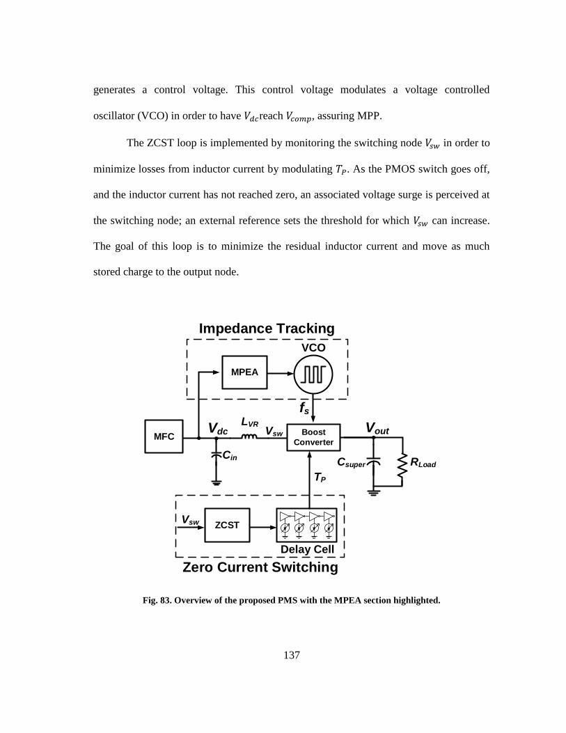
137
generates a control voltage. This control voltage modulates a voltage controlled
oscillator (VCO) in order to have 𝑉𝑑𝑐reach 𝑉𝑐𝑜𝑚𝑝, assuring MPP.
The ZCST loop is implemented by monitoring the switching node 𝑉𝑠𝑤 in order to
minimize losses from inductor current by modulating 𝑇𝑃. As the PMOS switch goes off,
and the inductor current has not reached zero, an associated voltage surge is perceived at
the switching node; an external reference sets the threshold for which 𝑉𝑠𝑤 can increase.
The goal of this loop is to minimize the residual inductor current and move as much
stored charge to the output node.
Fig. 83. Overview of the proposed PMS with the MPEA section highlighted.
Vout
Csuper RLoad
L1 Boost
Converter
Cin
Vdc
Impedance Tracking
fs
VCO
LVRVswMFC
MPEA
TP
ZCSTVsw
Zero Current Switching
Delay Cell

138
Fig. 84. Fundamental schematic of the boost converter used here as part of the PMS circuit.
The Experimental Results and Discussion section in this chapter present circuit
details and voltage references on both MPEA and ZCST loop implementations.
Circuit implementation for PMS
The boost converter in Fig. 84 is a voltage step-up converter capable of
increasing a DC voltage from the input (𝑉𝑑𝑐) to a higher DC output voltage value (𝑉𝑜𝑢𝑡).
Output current load and input power are the main limitations in terms of how much gain
(𝑉𝑜𝑢𝑡/𝑉𝑑𝑐) the converter can achieve.
The parameter utilized to modify the input impedance of the boost converter is
the switching frequency (1/𝑇𝑠). As the converter operates in DCM, the input impedance
is derived from the averaged inductor current [8]. The expression of the input impedance
can be approximated as:
Rload
L1
VdcLVR
MFCVout
NMOS
PMOS
VN
VP
Csuper
Vsw
Switching
Frequency
ZVR
ILVR
TN
TP

139
𝑍𝑉𝑅 ≈
2 ∙ 𝐿𝑉𝑅 ∙ 𝑇𝑠
𝑇𝑁2 =
2 𝐿𝑉𝑅
𝐷𝑢𝑡𝑦𝑐𝑦𝑐𝑙𝑒2 𝑇𝑠
(84)
where 𝐿𝑉𝑅 is the converter inductor, 𝑇𝑁is the on-time for the NMOS switch, and
𝐷𝑢𝑡𝑦𝑐𝑦𝑐𝑙𝑒 is the NMOS switch duty cycle. By defining the duty cycle for the NMOS
switch to be 50% of the period (𝑇𝑆), (84) yields:
𝑇𝑁 = 𝐷𝑢𝑡𝑦𝑐𝑦𝑐𝑙𝑒 ∙ 𝑇𝑠 = 0.5 ∙ 𝑇𝑠 (85)
𝑍𝑉𝑅 ≈
2 𝐿𝑉𝑅
0.52𝑇𝑠= 8 𝐿𝑉𝑅 𝑓𝑠
(86)
This allows the input resistance of the boost converter to vary in a linear fashion
to fulfill the needs of MPP for the MFC. This permitted the implementation of a
frequency-controlled input resistance of the PMS. From the system characterization and
specifications in the previous section (Adaptable Maximum Power Extraction
Algorithm), the input resistance to match is 𝑅𝑀𝐹𝐶 =400Ω. Thus,𝐿𝑉𝑅 was selected to be
1.5 mH, setting the switching frequency to 66kHz.Broad resistance matching ranges can
be obtained through different inductor and switching frequency values.
The PMS also possesses the capabilities of extracting power from much lower
producing MFCs. This lower power production is translated as an electrical equivalent
MFC source with larger 𝑅𝑀𝐹𝐶 . As shown in (4), the input resistance would modulate to
extract maximum power matching 𝑍𝑉𝑅 and 𝑅𝑀𝐹𝐶 .

140
Operating point for impedance tracking implementation
Fig. 85. (Left) Measured RC time constant (τMFC) of the MFC device and (right) illustration of time
needed to charge the capacitor C1 to read the open circuit voltage VMFC.
As mentioned in the previous Section (Adaptable Maximum Power Extraction
Algorithm), variable 𝜏𝑀𝐹𝐶 is measured and shown in Fig. 85. As with any RC circuit,
𝜏𝑀𝐹𝐶 is the time required to charge 𝐶𝑀𝐹𝐶 through resistor 𝑅𝑀𝐹𝐶 to ~63% of its final
value. It can be seen that the time it takes for the RC system to reach approximately 99%
of its final value is 40 seconds. This information, along with the characterized value of
𝑅𝑀𝐹𝐶 allows an estimation of 𝐶𝑀𝐹𝐶:
𝜏𝑀𝐹𝐶 = 𝐶𝑀𝐹𝐶𝑅𝑀𝐹𝐶 = 10 𝑠 (87)
From (87), for an 𝑅𝑀𝐹𝐶 = 400Ω, 𝐶𝑀𝐹𝐶 is approximately 25 mF. Note that under
circumstances where no 𝑅𝑀𝐹𝐶 is known through characterization, 𝜏𝑀𝐹𝐶from testing
alone can function as an indicator of MFC health, i.e. 𝜏𝑀𝐹𝐶 ≫ 10𝑠 is an indication of
141
weak MFC power production. The 𝜏𝑀𝐹𝐶 parameter serves as a strong indicator on the
MFC power delivery capabilities and PMS MPP method (Manual or Dynamic) needed
in order to achieve maximum power extraction. In summary, the MFCs time constant
sets the operation range of the PMS’s MPP method (Manual or Dynamic).
Fig. 86. Relationship between ϕ2 and ϕ1.
Fig. 86 illustrates the comparison between both clock phases 𝜙2 and 𝜙1. For the
characterized MFC and measurements the required time for the MFC to reach nominal
𝑉𝑀𝐹𝐶 is too large to be implemented practically in an integrated solution. For the
proposed PMS, a good rule of design is to minimize the sampling window (𝑇𝑠𝑎𝑚𝑝)
compared to the refresh rate (𝑇𝑅), since 𝑇𝑠𝑎𝑚𝑝 effectively disengages the MFC from the
PMS disrupting power delivery. Non-integrated solutions could potentially allow longer
𝑇𝑠𝑎𝑚𝑝 avoiding manual range operation.

142
The OCV sampling window is performed by phase 𝜙2 with duration 𝑇𝑠, and the
refresh rate is performed by phase 𝜙1 with duration 𝑇𝑅. A 1/8th
maximum 𝑇𝑠 value with
respect to 𝑇𝑅 for the PMS is suggested to minimize power disruption. For larger values
of 𝜏𝑀𝐹𝐶 , longer 𝑇𝑠𝑎𝑚𝑝is required; hence longer values for𝑇𝑅. This requires high capacity
sampling capacitors (𝐶1and 𝐶2) with low ESR to minimize leakage between each
sampling window in order to minimize MPP error. This assures limited power disruption
to the PMS, while correct MPP.
With the implemented approach of 1/8 ratio limit between sampling window to
sampling period careful considerations should be taken when sizing 𝐶1and 𝐶2. As 𝐶1 is
placed in parallel to the MFC, this would effectively increase the associated capacitance
with 𝜏𝑀𝐹𝐶 to be 𝐶𝑀𝐹𝐶+ 𝐶1. Therefore, 𝐶1should always be sized much smaller than CMFC
to avoid increasing 𝜏𝑀𝐹𝐶 beyond the 1/8 limit for fully monolithic approaches.
In Fig. 82, for values of 𝜏𝑀𝐹𝐶 lower than the time constant threshold, the
dynamic range is externally set. Fig. 87 shows the sampling structure for this mode of
operation; which allows for quick and dynamic OCV monitoring through two non-
overlapping control signals (Fig. 86) for the sampling switches.

143
Fig. 87. Operating point tracking for dynamic range, phase ϕ2 sampling of VMFC and phase ϕ2
dividing VMFC by two.
During 𝜙2 the open circuit voltage 𝑉𝑀𝐹𝐶 is stored in 𝐶1 (Fig. 87). During 𝜙1, the
charge stored in 𝐶1 is shared with 𝐶2 through the associated controlled switches. Since
both capacitors have the same value, the voltage at node 𝑉𝑐𝑜𝑚𝑝 becomes equal to 𝑉𝑀𝐹𝐶/2
due to charge redistribution between the two capacitors. Phase𝜙2 pulse duration, 𝑇𝑠𝑎𝑚𝑝,
needs to be at least equal to 4𝜏𝑀𝐹𝐶 (Fig. 85) in order for 𝐶1 to be charged to a value close
to 𝑉𝑀𝐹𝐶. The timing is achieved through a dedicated one-shot circuit with external tuning
to achieve the required sampling window for 𝜙2. Fig. 88 shows experimental correct
MPP being achieved under electrical equivalent circuit for a high powered MFC
(𝜏𝑀𝐹𝐶 = 5 ms).
VMFC
RMFC
CMFC Vs
Power
Management
System
Φ2
Φ2
Φ1
C1 C2
Vdc
Vcomp
Cin

144
Fig. 88. Dynamic range showing correct MPP.
For the measured MFC, with large value 𝜏𝑀𝐹𝐶 , the manual range is externally set.
In order for the MPP be achieved without large power disruption to the PMS, a pre-
charging scheme for the sampling capacitors (𝐶1and 𝐶2) is employed. This eliminates the
need to disengage the PMS from the MFC required to sample the open circuit voltage
(𝑉𝑀𝐹𝐶 = 𝑉𝑠). Fig. 89 shows the manner in which the manual range achieves the
characterized 720 mV of the MFC. The pre-charging scheme is implemented through a
similar sampling approach as the dynamic range, but without sensing the MFC’s OCV,
through a resistor divider from 𝑉𝑜𝑢𝑡. Since the output voltage node is set to a fixed value
(2.5 V), the MPP can be obtained via a divider network. The same sampling phases,
𝜙2and 𝜙1, are used to obtain 𝑉𝑐𝑜𝑚𝑝.
Vdc
~360 mV (MPEA)
720 mV
~360 mV
Vcomp

145
The threshold, 𝜏𝑀𝐹𝐶 , for the dynamic/manual range is set to 25 ms. This allows a
sampling window of 100 ms (4 𝜏𝑀𝐹𝐶) to be applied with a 800ms value for 𝑇. From (88),
solving for 𝑅𝑡𝑢𝑛𝑒 sets this resistor value to 404 kΩ, with a 1 MΩ value for 𝑅𝑥, to achieve
720 mV from the 2.5 V at the output node.
𝑉𝑐𝑜𝑚𝑝 = 𝑉𝑜𝑢𝑡
𝑅𝑡𝑢𝑛𝑒
𝑅𝑥 + 𝑅𝑡𝑢𝑛𝑒
(88)
Fig. 90 shows the correct MPP being achieved for the system tested in Fig. 85
through the pre-charging scheme proposed for the PMS. A note of importance is to
consider capacitance values capable of maintaining correct charged voltage over the
entirety of 𝑇𝑅. Issues such as leakage must be carefully accounted for otherwise voltage
𝑉𝑐𝑜𝑚𝑝 will negatively affect the MPEA loop.
Fig. 89. Operating point tracking for manual range, (ϕ2) sampling of Vout and (ϕ1) dividing Vcomp by
two.
Power
Management
System
Φ2
Φ1
C1 C2
Vdc
VcompRx Vcomp
Vout
Φ2
Rtune
Switch disengaged
Switch locked in
closed position
MFC
Φ2

146
The proposed MPP acquisition effectively reduces the required time for the PMS
to locate and operate at MPP compared to conventional polarization curve approaches
[39].
Fig. 90. Manual range showing correct MPP.
It should be noted that if the OCV were to drastically change from the set MPP
voltage through the resistive divider, maximum power extraction would not be achieved.
A possibility would be to reset the resistive divider to recalibrate to MPP. Nonetheless, it
is well documented [122, 123] that MFC OCV does not vary significantly over long
periods of time.

147
MPEA implementation
Fig. 91 present the main blocks which make up the dynamic MPEA. Once the
desired operating point is stored in 𝐶1 (𝑉𝑐𝑜𝑚𝑝 from Fig. 87, Fig. 89), this is compared to
the value at the input of the boost converter (𝑉𝑑𝑐).
Fig. 91. Impedance tracking scheme for MPEA.
Depending on the voltage level of 𝑉𝑑𝑐, a comparator sets a control voltage for a
VCO, implemented by a ring-oscillator, in order to modify the input impedance of the
boost converter and match 𝑅𝑀𝐹𝐶 .
The implemented charge pump injects packets of charge into the control voltage
node (𝑉𝐶1) through externally biased switched current sources.
Voltage Controlled OscillatorComparator
Vcomp
Vc1
Vdc
Off chip
Off chip
Impedance Tracking VoutVext
fs

148
Zero current switching tracking loop
A critical component regarding efficiency is the duration of 𝑇𝑃 (PMOS on-time
duration). Previous methods have proposed setting a fixed period [17] or toggling values
to reduce reverse inductor current losses [8]. While these efforts improve on
synchronous switching they still lack fine tuning capabilities to minimize losses due to
inductor current achieving negative values.
As previously explored in [8, 17], when the PMOS switch switches off, and the
inductor current has not reached zero, an associated voltage surge is perceived at the
switching node (𝑉𝑠𝑤 Fig. 83) of a boost converter. This voltage surge, shown in Fig. 92,
is proportional to the rate of change of the remaining current in the inductor when the
PMOS switches off. Ideally the inductor current would fall to zero before the PMOS is
switched off, thus, reducing any losses associated with this switch (Fig. 92). The
proposed solution to minimizing these potential losses associated with negative inductor
current is through a dynamic Zero Current Switching Tracking (ZCST) loop.
Fig. 93 shows how the tuning of the 𝑇𝑃 parameter is tuned via the ZCST loop.
The process behaves in the reverse manner when the inductor current falls below zero.
As with the Impedance Tracking loop, the ZCST loop requires externally biased
current sources in order to deliver a 𝑉𝑐2 to the inverter delay cells. The 𝑉𝑠𝑤 node surge
upper limit is determined through an external reference,𝑉𝑧𝑟𝑒𝑓, tuned to minimize
inductor current losses.

149
Fig. 92. Inductor current and ZCST parameters.
Fig. 93. Zero current switching tracking loop for Tp time control.
ILVR
VP
VSW
Vc2
TN
Detected
voltage surge
TP
t1 t2 t3 t4
TP
Vzref
Comparator
Vsw
Vzref
Zero Current Switching Tracking
Vc2
VN VN,Delay
VoutVext
Off chip
Off chip
NMOS Clock Delay Cell

150
The ZCST loop minimizes the losses from the inductor current by setting 𝑇𝑃 time
through an adaptive inverter delay cell controlled by the comparison of the voltage surge
from 𝑉𝑠𝑤 and 𝑉𝑧𝑟𝑒𝑓. Whenever the voltage surge exceeds 𝑉𝑧𝑟𝑒𝑓, the control voltage 𝑉𝑐2
starves the delay cell of available current, effectively slowing down the signal 𝑉𝑁,𝐷𝑒𝑙𝑎𝑦
used to generate the PMOS signal (𝑇𝑃) [8]. VP determination is next discussed.
Output voltage setting
The output node voltage, 𝑉𝑜𝑢𝑡, is constantly monitored by a secondary comparator that
turns the entire PMS on or off depending on the reference voltage level, 𝑉𝑅𝐸𝐹; if 𝑉𝑜𝑢𝑡
exceeds the set reference voltage, the system automatically stops operating and waits
until 𝑉𝑜𝑢𝑡drops below the reference level. This is common practice in energy harvesting
power management systems [17, 86, 97, 121]. To assure that enough conversion gain is
achieved by the boost converter, 𝑇𝑃 is set much smaller than the 𝑇𝑁. Fig. 77 shows how
the 𝑇𝑃 (VP) signal is obtained from the 𝑉𝑁,𝐷𝑒𝑙𝑎𝑦 signal (ZCST) and logic gate approach
(Fig. 94).
Fig. 94. VP generation for TP signal.
VN,Delay
VN
VP

151
The small value of 𝑇𝑃assures enough conversion gain as stated by the conversion
gain equation [20]:
𝑉𝑜𝑢𝑡 ≈ (1 +
𝑇𝑁
𝑇𝑃) ∙ 𝑉𝑖𝑛
(89)
Setting a high value for (1 +𝑇𝑁
𝑇𝑃) always assures to be enough to achieve 2.5 V at
the output. The conversion gain (𝑉𝑜𝑢𝑡/𝑉𝑖𝑛) is always maximized through the ZCST loop,
minimizing inductor current losses.
Fig. 95 shows how the output voltage setting is performed. In order to fix the
output voltage, a global enable is employed through a division of 𝑉𝑜𝑢𝑡 and comparing it
to a 1.25 V reference.
Fig. 95. Internal voltage supply for controller and driver acquisition fromVout.
Boost Converter Vout
Vout /2
Csuper
Internal VDD
enable
VREF
÷2
VCO

152
Power management system startup
As the output voltage level of the MFC is not high enough to allow for self-
starting operation from the PMS. An external one-time pre-charging of the output
capacitor to 900 mV is required to begin controller operation. Multiple different
approaches may be taken to startup the system [88, 124].
Once the system begins extracting energy from the MFC, there is no longer need
for an external power source to power the PMS.
Experimental results and discussion
Fig. 96 showcases the testing setup for the complete PMS. The complete PMS was
fabricated in 0.5 μm CMOS technology with an active area of 0.8mm2, die photograph is
shown in Fig. 97. The measurements were performed with a storage capacitor 𝐶𝑖𝑛 of
10mF, a super-capacitor 𝐶𝑠𝑢𝑝𝑒𝑟 of 0.1 F, and external biasing and references.
Fig. 96. Overall testing setup to characterize the PMS controlling the MFC.
Power
Management
System MFC
Vout
CsuperCin
Oscilloscope
Voltage
References
Biases
ILoad

153
Fig. 97. Die microphotograph.
To begin testing the steps taken are the following: i) biases for both MPEA and
ZCST are set externally through off-chip supplies, ii) the output voltage reference of
1.25 V is set for the Output Voltage Setting block, iii) Reference 𝑉𝑧𝑟𝑒𝑓 set to 625 mV for
the ZCST block, iv) the manual range is set, for the presented MFC, through an external
pin set to the lowest potential (not shown in Fig. 20), and finally v) testing is performed
by an external initial pre-charge on 𝐶𝑠𝑢𝑝𝑒𝑟 to 900 mV. The pre-charge allows the control
circuit to being switching operation and extraction from the MFC follows.
Maximum power extraction algorithm
Fig. 98 showcases the MPEA correctly achieving MPP at 360 mV with a
switching frequency of approximately 65 kHz. Measurements were performed by pre-
charging the output capacitor, 𝐶𝑜𝑢𝑡, to 900 mV to allow the system to begin operating.
ZC
STPMOS +
Drivers
MPEA
NMOS +
Drivers
ZCST
Output
Voltage
Setting
1 mm
0.8
mm

154
Fig. 98. Input and output voltage profiles at steady state with ~75μA load.
The manual range was externally set with 𝑅𝑡𝑢𝑛𝑒 sets to 404 kΩ, with a 1 MΩ
value for 𝑅𝑥, to achieve 720 mV from the 2.5 V at the output node
It should be noted that frequency variations are to be expected due to the
continuous comparison between 𝑉𝑠 and 𝑉𝑐𝑜𝑚𝑝 that results in dynamic toggling of the
control voltage 𝑉𝑐1 (Fig. 93) to vary slightly around the correct operating point. The
output voltage value of approximately 2.5 V was successfully achieved with a load of
~75 μA.
Zero current switching tracking
Fig. 99 shows the ZCST loop minimizing the voltage surge from the early PMOS
off time. 𝑉𝑧𝑟𝑒𝑓limits the voltage surge related to 𝑉𝑠𝑤 (Fig. 83).

155
Fig. 99. ZCST loop minimizing losses from inductor current switching.
The external reference 𝑉𝑧𝑟𝑒𝑓 was set to 625 mV as the threshold for the voltage
surge detection at node 𝑉𝑠𝑤. Voltage surges detected at 𝑉𝑠𝑤can be seen effectively
decrease as the ZCST loop increases 𝑇𝑃 to minimize residual inductor current.
Total power consumption and efficiency
Fig. 100 shows overall power consumption for both static (quiescent) and
dynamic; total power consumed is 13.16μW.

156
Fig. 100. Overall PMS power consumption breakdown.
Fig. 101 shows the efficiency profile. The efficiency of the PMS was measured
for varying loads. Maximum efficiency was recorded at ~58% with a load of ~250 μW.
TABLE 10 summarizes and compares the presented solution to previously reported
systems. It should be noted that the proposed solution is the only system possessing
quiescent power consumption below 1 μW, as well as taking circuit dynamic power
consumption into account in the efficiency measurements. Efficiency is considered
dynamic as it does not take into account the effects of the 1 μW quiescent; this is
performed in the same fashion as references in TABLE 10. Thus, the presented PMS
achieves a significantly higher efficiency compared to previously reported PMSs for
MFCs.
MPP Acquisition
(100 nW)
Switching
Losses
(8.25 µW)
Output
Voltage
Setting
(3.9 µW)
MPEA
(500 nW)
ZCST
(350 nW)
Dynamic Power
Consumption
Static (Quiescent)
Power Consumption

157
TABLE 10. Comparison of MFC power management units.
SPECIFICATION [102] [125] [6] [126] [107] THIS WORK
Input Voltage
Range 300mV
300mV*
180mV** 300mV
300mV
(startup at
140mV)
300mV 300mV-720mV
Output Voltage 1.8V 3.3V 2.5V 1V 3.3V 2.5V
Inductor 2μH
7.5μH**
(primary winding
transformer)
110mH
326.7μH
(primary
winding)
1:20 transformer 1.5mH
Output
Capacitor 47μF
0.25F*
1.5F**
(supercapacitors)
1F
(supercapacitors) 8μF
680μF
0.4F
(supercapacitor)
0.1 F
(supercapacitor)
Maximum
Power
Extraction
- - Hysteresis
Control - -
Adaptable
MPEA tracking
Max. Efficiency - 5.33%*
4.29%** - 73%† 53%† 58%‡
Implementation
Approach
Discrete
Components
Discrete
Components
Discrete
Components
Discrete
Components
Discrete
Components Custom IC
*Charge Pump + Boost converter topology
**Transformer + Boost converter topology
†Does not take into account system power consumption
‡ PMS operates with <1μW of quiescent power consumption

158
Comparison between similar CMOS implementations focused on extracting
maximum power from energy harvesting sources, other than MFCs, would require
higher power for the MPP control) [20, 127-129] compared to the proposed MPEA
presented (~600 nW for only the MPEA control). It should be noted that switching
losses, comprising the majority of the circuits’ power consumption, can potentially be
reduced if the system were to be implemented in a smaller technology, i.e. 180 nm
CMOS process or smaller.
Discussion
While the use of the pre-charging scheme for the proposed PMS is implemented,
an alternative approach would be to directly power from a battery at 𝑉𝑏𝑎𝑡𝑡, as seen in
Fig. 102. While the battery is needed to start the system and deliver the appropriate
biases and references at startup, once the system begins extracting power from the MFC,
it can then store the extracted energy back into the battery.
Fig. 101. Measured efficiency vs. delivered power.
0
10
20
30
40
50
60
70
0 50 100 150 200 250 300
Eff
icie
ncy
(%
)
Delivered Power (µW)

159
Both references and biases, used in the ZCST and MPEA, would potentially be
generated internally through low-power integrated temperature stable reference
consuming sub-µWs of power [130, 131] (bandgap voltage references). Due to the low
power extracted from the MFC (~320 µW) a rechargeable battery can be directly
charged from the PMS output with the assurance no damage to the chemistry will occur.
This scenario would be plausible with MFCs delivering power over 13.6 µW
(dynamic power of 12.25 µW +static power of 0.85 µW) plus the additional reference
power requirements from the temperature stable references. This possible scheme would
enable a much longer up-time operation for the wireless sensor. A small amount of
invested power to increase the system’s operational lifetime would be the requirement.
Fig. 102. Possible implementation with presented PMS for battery extending operation.
VbattVdcMFC
Step-up +
ZCST
Boost Converter
MPEA
Impedance
Tracking
RMFC
ICharge
Cin
ZVR
Battery
Biases + References

160
Conclusions
MFCs can generate renewable energy from waste organic substrates such as
wastewater and other biomass by using the metabolic process of electrochemically active
bacteria. Due to their inherently low power and voltage profiles however, power
management systems are required to process the MFC power to a usable voltage levels
such as CMOS compatible voltage. This chapter presents a singular dynamic MPEA
DC-DC converter IC chip for efficiently managing power outputs of MFCs.
The presented monolithic boost converter is capable of sampling and locating the
MPP and setting the input resistance to match that of the internal MFC resistance, hence
continuously operating the system at MPP. Previous works cannot accomplish this with
the MFC’s complex impedance. This proposed solution presents a quicker approach to
MPP compared to conventional MFC characterization through polarization curve
approaches. The MPEA is capable of dynamically matching the impedances of the MFC
that continuously changes over time. The MPEA also continuously extracts maximum
power from the MFC even when its power level changes over time. In order to reduce
inductor current losses by modulating 𝑇𝑃 time duration a ZCST loop is introduced. The
PMS was fabricated using a 0.5μm CMOS technology and demonstrated a maximum
dynamic efficiency of ~58% for a load of ~250μW.

161
CHAPTER V
AN INDUCTORLESS DC-DC CONVERTER FOR AN ENERGY AWARE POWER
MANAGEMENT UNIT FOR MICROBIAL FUEL CELLS*
Introduction
The research behind novel renewable energy sources has always been a critical
and major driving force in technological innovation. One of the breakthroughs in
renewable energy technologies has been the development of new and highly efficient
power management units (PMU) for energy harvesting (EH) systems. EH-PMUs are
focused on two major tasks: 1) extract maximum power from the renewable source, and
2) offer an acceptable and well-regulated voltage/current profile for the power delivery
chain.
Major results have been accomplished for several different EH sources, i.e.,
solar, kinetic, RF, and thermoelectric [132-135]. However, fully integrated solutions
where biomass is used as a source are still few, and PMU solutions have yet to tackle
extreme low power producing systems such as microbial fuel cells (MFC) [136]. Due to
their inherent low power production, power extraction from MFCs requires extremely
efficient and low power PMUs.
The power profile of an MFC varies with pH level, temperature, and amount/type
of substrate in the anode chamber [118, 137]. Over time, these aforementioned effects
* Reprinted with permission from “An Inductorless DC-DC Converter for an Energy Aware Power
Management Unit Aimed at Microbial Fuel Cell Arrays” by S. Carreon-Bautista, C. Erbay, A. Han, and E.
Sanchez-Sinencio, 2015. IEEE J. of Emerging and Selected Topics in Power Electronics, Early Access
Article, 2015, © 2015 IEEE

162
compound and reduce the maximum power delivered by the MFC. This overall power
degradation or fluctuation limits the potential of applying a single MFC for a continuous
load demanding system for any long up-time operation, and an MFC system would
require careful monitoring of the MFC health. A possible solution lies in implementing a
large volume MFC in order to maintain up-time for as long as possible [102] or
intermittent operation of PMUs [138]. Efforts of placing multiple devices in series or
parallel configuration are possible in order to improve either output voltage (series
connection increases equivalent output voltage), or reduce internal equivalent resistance
(parallel connection increases current delivering capability). However, due to the
nonlinear effects of the bacteria in MFC, variations in power production between devices
leads to unequal voltage drop when placed in an array fashion and hence, limiting the
overall power delivered by the array [139]. In fact, no current solution truly tackles the
low power density and wide range MFC parameters over time.
The proposed solution is to perform a time multiplexing harvesting approach,
where MFCs are harvested individually at MPP to avoid the issue of voltage reversal, yet
benefiting from an a higher power density achieved from an array configuration. The
present chapter presents an inductorless DC-DC converter (I-DCDC) which allows for
dynamic tracking of the optimum point for maximum power extraction from an MFC
array. The I-DCDC is part of an Energy Aware Power Management Unit (EA-PMU),
comprised of a power sensing and aforementioned I-DCDC converter. The I-DCDC is
implemented with a Charge Pump Dickson topology [57]. The EA-PMU performs a
power detection (PD) algorithm that locates the optimum MFC within the MFC array for

163
power extraction. Once the best MFC is located, the I-DCDC begins harvesting from the
selected MFC through a rewiring process, achieving maximum power point tracking
(MPPT) via a frequency modulation scheme (FMS). The proposed system is a novel
approach towards tackling MFC power profile degradation due to MFC internal
variations and towards effectively increasing power extraction by implementing a
multiplexing harvesting of MFC arrays.
MFC array and power extraction methodology
An MFC possesses nonlinear behavior when mapped to an equivalent electrical
circuit with initial approximations showing the effects of non-idealities [117, 118]. As
power is being extracted from an MFC, its performance degrades over time and delivers
less power if not replenished with a feeding solution. Another set of factors affecting
power performance of an MFC are: size, pH, temperature, and substrate concentration in
the anode chamber [118]. This causes challenges in maintaining a certain level of power
and voltage for the load.
For the proposed application, an MFC array is established from which maximum
power can be extracted from individual cells, maximizing the overall system efficiency.
Under this scheme, power from an individual MFC is harvested without the need of
previously knowing the optimum point of power extraction, contrary to previous
solutions implementing [140] multiple MFCs, the proposed converter can achieve MPP
power extraction at all times. The MPPT scheme locates and dynamically adjusts the
system parameters for the power converter to achieve a maximum power extraction.

164
The power detection of MFCs is performed in order to quickly switch between
the healthiest cells within the array. Once the healthiest MFC is selected, the PD
algorithm continues monitoring the rest of the array for a set period of time and selects
the best available candidate. The PD algorithm can be implemented in a variety of ways
such as: a microcontroller or a fully-integrated Finite-State-Machine (FSM).
State-of-the-art
Current power management solutions implementing MFCs as their power source
are limited in application and require large external components (inductor) [102, 136,
141], or suffer from complex implementation [142]. The issue of power degradation and
functional array implementation of MFCs has yet to be tackled in an efficient and
automated manner.
Previous efforts aimed at placing harvesting sources in an array fashion [112]
consider only resistive components when achieving MPP. Since the impedance the MFC
yields both resistive and reactive components, any array type approach where rapid
reconnection occurs between the DC-DC converter and the MFCs must tackle stability
issues in a more stringent fashion. Another multi-source approach with an LC switching
converter, which differs from the dynamics of a fully integrated capacitive DC-DC
converter, has also been presented [112]. The proposed implementation via a fully
capacitive DC-DC converter alone requires new understanding on the I-DCDC’s
particular interaction with the MPPT control loop.

165
Thus, this type of approach requires a sound implementation in order to tackle
the different MFC power profiles, and to show how energy harvesting MPPT control
loop dynamics are affected by it.
MFC construction and operation
Fig. 103. a) Schematic of a two chamber microbial fuel cell. b) The small (MFC-L) and large (MFC-
H) devices used with I-DCDC.
MFCs are bio-electrochemical, energy-producing devices that convert chemical
energy into electrical power by the catalytic activity of living bacteria. MFCs are similar
to other fuel cells, consisting of anode and cathode chambers separated by a proton
exchange membrane (PEM) as shown in Fig. 103a. In the anode chamber, fuel is
oxidized by the bacteria, generating CO2, electrons and hydrogen atoms. The electrodes
in each chamber connected through a resistor load and generated electrons are
166
transferred to the cathode electrodes, while protons are moved to the cathode chamber
through the membrane.
The MFCs were assembled by connecting two acrylic chambers separated with a
PEM (Nafion 117TM
, Ion Power Inc.). Carbon felt (Morgan, UK) was used as the anode
and carbon cloth with Pt catalyst on one side (10wt% Pt/C, 0.5 mg Pt/cm2, ElectroChem,
Inc.) was used as the cathode. Anaerobic activated sludge (Austin Wastewater Plant)
was used as the inoculum. The anode chamber was filled with wastewater, containing 1
g/L acetate and autoclaved anaerobic nutrient mineral buffer (NMB, pH 7.0) solution
[113]. Two different size MFC configurations were used to test the EA-PMU. The larger
MFC (MFC-H) had 1 L total volume with 100 cm2 anode and 50 cm
2 cathode electrode
areas. The smaller MFC (MFC-L) had 20 mL total volume with 2 cm2 anode and 1 cm
2
cathode electrode areas, both MFC devices can be seen in Fig. 103b. The cathode
chambers were filled with potassium ferricyanide (100 mM). During the startup phase,
the MFC was connected with an external resistor (1 kΩ), and the voltage across the
resistor was monitored through a multiplexer (National Instruments) for continuous
voltage measurements via a LabVIEWTM
(National Instruments) interface [114, 115,
143] and additional acetate was fed intermittently when the voltage generation was
lower than 50 mV. A polarization curve was obtained by varying the load resistances (10
Ω-50 kΩ).

167
MFC electrical equivalent circuit
Power profile tests were performed on multiple MFCs, showing that ranges for
series resistances (𝑅𝑀𝐹𝐶) varied from 100 Ω to 8 kΩs, with open circuit voltages ranging
from 600 mV to 800 mV. A second critical issue regarding the electrical equivalent
circuit for an MFC is the parasitic capacitance associated with the MFC (𝐶𝑀𝐹𝐶) ranging
from 6.5 μF to 2.5 mF. Both associated components (RMFC and CMFC) seen in Fig. 104
affect the maximum power extraction parameters for a power conversion system.
Fig. 104. Simplified electrical equivalent circuit for an MFC device.
Multiple characterization trials were performed on the MFC devices within the
array in order to quantify both associated components. TABLE 11 summarizes upper
and lower values obtained through the characterization process for the 20 mL MFC
(MFC-L) and 1 L MFC (MFC-H).

168
Obtaining these parameters for high/low power MFCs is critical in the design of
the I-DCDC converter in order to assure MPPT stability ranges after reconnection
between cells.
TABLE 11. Microbial fuel cell parameters
SPECIFICATION VALUE RANGE
𝑹𝑴𝑭𝑪 0.1 𝑘Ω − 8 𝑘Ω
𝑪𝑴𝑭𝑪 6.5𝜇𝐹 − 2.5𝑚𝐹
𝑽𝑴𝑭𝑪 600𝑚𝑉 − 800𝑚𝑉
Inductorless DC-DC converter
Fig. 105 presents the proposed overall structure of the EA-PMU with the I-
DCDC block being featured in this article. Section IV-C further elaborates on the design
and specifications of the converter. The I-DCDC converter is comprised of a variable
stage, 10X Dickson charge pump (CP) capable of dynamically achieving MPPT over a
wide range of MFC impedance scenarios. The number of stages in the CP is
automatically set depending on input voltage and load current conditions of the
converter through a stage control loop monitoring the output voltage node. Likewise, a
frequency modulation scheme (FMS) is also implemented in order to achieve automatic
input resistance matching through an MPPT loop, between the converter and the MFC
input resistance (𝑅𝑀𝐹𝐶). MFCs behave as DC voltage sources, where variations
occurring on the DC voltage of the MFC can be considered negligible i.e. low frequency,

169
the maximum power transfer theorem states [120] that maximum power is transferred
when a DC source (𝑉𝑀𝐹𝐶) with fixed source resistance (𝑅𝑀𝐹𝐶) is connected to a load
resistance (𝑅𝑖𝑛) of equal value to the source resistance, causing the input voltage to be
𝑉𝑀𝐹𝐶/2 (𝑉𝑀𝑃𝑃 in Fig. 105). A capacitive divider is implemented to obtain the correct
reference of 𝑉𝑀𝑃𝑃. As the PD algorithm switches within the MFC array, the MPPT
control loop must assure that the I-DCDC converter reaches MPP in a fast and stable
manner. Since MFCs are selected based on their power availability, it is possible that
this can result in switching between a low-power (high valued 𝑅𝑀𝐹𝐶 and 𝐶𝑀𝐹𝐶) cell to a
high-power (low valued 𝑅𝑀𝐹𝐶 and 𝐶𝑀𝐹𝐶) cell.
Fig. 105. Proposed structure of the energy aware-power management unit.

170
Since the process of extracting power from the MFCs follows a time interleaved
approach, the reconnection scenario can potentially result in a faulty and unstable MPP
acquisition due to the strong effect of switching between low- and high-power producing
MFCs (small and large values of 𝑅𝑀𝐹𝐶 and 𝐶𝑀𝐹𝐶). Stability considerations will be
further discussed in the following section titled: Maximum Power Extraction for MFC
Arrays.
Maximum power extraction for MFC array
The main goal of the MPPT control loop is to achieve resistive matching,
between 𝑅𝑀𝐹𝐶 and 𝑅𝑖𝑛, in order to ensure maximum power transfer from any individual
MFCs within the MFC array by modulating the switching frequency. Frequency
modulation is commonly used in low-power applications where efficiency at light loads
and low power consumption of control circuitry are critical [55]. FMS was selected for
the control method since traditional approaches, which have variable duty cycles have a
limited effective control range over which regulation may be applied on capacitive DC-
DC converters [62, 144]. The downside of the FMS approach is that the noise spectrum
and EMI for successive blocks in the power chain is increased. Since the proposed EA-
PMU application is intended for intermittently operating sensor nodes, a large storage
capacitor at the output of the converter offers significant noise suppression.
As with most energy harvesting applications, the main focus of the EA-PMU is
to deliver as much power from the harvesting source to the load at the appropriate
voltage levels.

171
Once the voltage levels are attained, the controller is disengaged to minimize
power consumption. Two main operating conditions are determined: storage efficiency
and current demanding load scenario. For the first condition, multiple storage capacitors
can be sequentially charged in order to keep the PMU operating for long periods of time.
For the second condition, a load demand proportional to the input power from the MFC
requires the system to maintain operation in order to achieve the required output voltage.
The output voltage regulation aspect of the converter is achieved by fixing the output
voltage to a predefined level by always extracting maximum power from the input
source. Any load demand beyond the available input power (operating at MPP), would
result in a voltage drop at the output of the any converter.
Input resistance for I-DC DC
As mentioned in the previous section, the source resistance range of the MFCs
characterized were between 100 Ω to 8 kΩs. This indicates that the proposed converter
must be capable of matching these values to its own input resistance. In order to
calculate for the input resistance of the converter, the procedure established in [145, 146]
allows for quantification of the input resistance with averaged values for input and
output voltages. For the step-up Dickson CP topology, assuming ideal charge transfer
switches, the expression for the input resistance is:
𝑅𝑖𝑛 =
𝑉𝑖𝑛
𝐼𝑖𝑛=
𝑁
𝐴𝐼𝑑𝑒𝑎𝑙 𝐶𝑖 𝑓𝑠𝑤 𝛥𝐴𝑔𝑎𝑖𝑛
(90)

172
where the components in 𝑁, 𝐶𝑖, 𝑓𝑠𝑤, 𝐴𝐼𝑑𝑒𝑎𝑙, and Δ𝐴𝑔𝑎𝑖𝑛 are the number of stages,
capacitance per stage, switching frequency of the converter, ideal voltage gain
expression (𝐴𝐼𝑑𝑒𝑎𝑙 = 𝑁 + 1), and difference between actual voltage gain expression
(𝐴𝑉 = 𝑉𝑜𝑢𝑡/𝑉𝑖𝑛) and the ideal gain (Δ𝐴𝑔𝑎𝑖𝑛 = 𝐴𝑖𝑑𝑒𝑎𝑙 − 𝐴𝑉). AV calculated assuming
ideal charge transfer switches yields:
𝐴𝑉 = (𝑁 + 1) ∙ (1
1 +𝑁
𝐶𝑖 𝑓𝑠𝑤 𝑅𝐿𝑜𝑎𝑑
) (91)
Δ𝐴𝑔𝑎𝑖𝑛 =
𝑁 + 1
1 +𝐶𝑖 𝑓𝑠𝑤 𝑅𝐿𝑜𝑎𝑑
𝑁
(92)
The first term of 𝐴𝑉, (N + 1), is the ideal voltage gain of the converter and the
second term makes up the efficiency of the system and how it is affected by number of
stages (N), frequency, and load. A more elaborate efficiency expression, including effect
of parasitic capacitances, is found in [67]. As stages increase, both input resistance and
overall efficiency decrease.
Fig. 106 presents the variable input resistance range of the I-DCDC for an
increasing number of stages (𝑁) [42], and switching frequencies for the converter. As
the number of stages is reduced the equivalent input resistance range for a given
switching frequency is also decreased, requiring higher switching frequencies to match
low 𝑅𝑀𝐹𝐶 values.

173
Fig. 106. Input resistance variation for inductorless DC-DC converter.
From (90) the input resistance is inversely proportional to capacitance per stage
(𝐶𝑖) and switching frequency (𝑓𝑠𝑤) as would be expected from a switched capacitor
circuit. A value of ~200 pF for each stage capacitance was selected in order to maintain
switching frequency to a minimum range allowing for system-wide low power
consumption. The main tradeoff with this approach is area cost due to the capacitance
density offered by the process used (4.1 fF/μm2 in 0.18 μm CMOS process) and the high
switching frequency required for high power MFCs (low 𝑅𝑀𝐹𝐶 values).
Previous efforts [42] implementing stage addition/subtraction as the main
mechanism for maximum power extraction show a limited range over which matching

174
can be performed when compared to the wider matching range offered by sweeping the
switching frequency and stage management offered by the proposed solution. Fig. 3
highlights the flexibility offered by the EA-PMU compared to the approach proposed by
[42].
For maximum power transfer to occur, the I-DCDC’s input resistance must equal
𝑅𝑀𝐹𝐶 . Once the input voltage of the converter equals to half of the MFC’s open circuit
voltage, the maximum power transfer [120] condition occurs. Since MPP is achieved
through a control loop dependent on input impedance, stability issues are vital to the
correct operation of the system once reconnection between MFCs occurs. Switching
between different MFCs will cause impedance variations at 𝑉𝑖𝑛 of the I-DCDC,
requiring the system to modulate its input resistance to correctly achieve MPP. Fig. 107
shows the small-signal model of the MPPT system. With each reconnection of an MFC,
a new impedance profile is presented to the PMU, requiring quick and accurate matching
Fig. 107. Small-signal equivalent MFC source impedance for control-to-input transfer function.

175
within as short amount of time as possible. The proposed PMU is unique in this aspect,
since modification of the input source modifies the control loop parameters demanding
the PMU’s MPPT loop to possess a stable response under all conditions it may face from
the MFCs within the array.
I-DCDC stability with reconnection
In order to take frequency behavior into consideration for stability concerns of
the MPPT loop, a small-signal model for the switching converter is elaborated. Contrary
to the work presented in [112], the switching frequency is inversely proportional to the
input resistance of the I-DCDC converter, nor is there an associated internal parasitic
capacitance found in TEG sources. State-space averaging following [60] was performed
to obtain the control-to-input (C-to-I) transfer function, where individual variables for
the on and off (Ton and Toff) time for a switching converter are implemented. Through
analysis, the C-to-I transfer function for the converter yields:
𝑉𝑖𝑛(𝑠)
𝑉𝑐(𝑠)=
𝐺𝑑𝑜
𝑠 + 𝜔𝑝𝐾𝑐𝑐𝑜
≈
𝑇𝑜𝑛
𝑅𝑜𝑛 𝐶𝑀𝐹𝐶(Vout,DC − (𝑁 + 1)Vin,DC)
𝑠 + (1
𝑅𝑀𝐹𝐶 𝐶𝑀𝐹𝐶+
((𝑁 + 1)𝑇𝑜𝑛𝐹𝑠𝑤)𝑅𝑜𝑛 𝐶𝑀𝐹𝐶
)
𝐾𝑐𝑐𝑜
(93)
𝜔𝑝 ≈
𝑅𝑜𝑛 + 𝑅𝑀𝐹𝐶((𝑁 + 1) ∙ 𝑇𝑜𝑛𝐹𝑠𝑤)
𝐶𝑀𝐹𝐶 ∙ 𝑅𝑀𝐹𝐶𝑅𝑜𝑛
(94)

176
where 𝑁, 𝐾𝑐𝑐𝑜, 𝑅𝑝𝑎𝑟, and 𝐶𝑀𝐹𝐶 are the number of stages in the converter, the oscillator
linear gain, the equivalent parallel resistance (𝑅𝑝𝑎𝑟 = 𝑅𝑀𝐹𝐶||𝑅𝑜𝑛) of the MFC’s series
resistance and switches’ on resistance, and parasitic capacitance, respectively. 𝑇𝑜𝑛 and
𝑇𝑠𝑤 are the on-time duration of a switching period and switching period times, and
finally, 𝑉𝑖𝑛,𝐷𝐶 and 𝑉𝑜𝑢𝑡,𝐷𝐶 from (92) are the steady-state DC voltages at the input and
output of the converter and are obtained from the state-space DC averaging (see
Appendix). Equation (93) shows the pole location given by the 𝐶𝑀𝐹𝐶 value and
resistances 𝑅𝑀𝐹𝐶 and 𝑅𝑜𝑛. Equation (92) behaves as a single pole system below the
switching frequency of the converter. From here, it is clear to see that the pole is
dominated mainly by the MFC parasitic electrical equivalents, which vary over a large
range (TABLE 11). Fig. 108 shows both simulated and analytical expressions in good
agreement between obtained transfer function and its simulated performance.
Fig. 108. Control-to-input simulated and analytical comparison.

177
The small signal equivalent model for the MPPT loop (Fig. 105) is shown in Fig.
109, where the open loop transfer function, 𝑇𝑜𝑙(𝑠), is given by:
𝑇𝑜𝑙(𝑠) = 𝐵(𝑠) 𝐾𝑝 𝐾𝑐𝑝 𝐹(𝑠) (95)
where Kp, Kcp, F(s), and B(s) are the comparator gain, current steering charge pump
gain, filter transfer function, and the C-to-I transfer function of the converter. As was the
case in [112], loop performance can be enhanced through the implementation of a filter
block, F(s).
Fig. 109. Small-signal stability model for PMU MPPT scheme.
The open loop transfer function without considering an optimized filter (𝐹(𝑠)
implemented with a 10 nF capacitor), with 𝐾𝑐𝑝 of 100 nA quiescent current and 𝐾𝑝 of
100 dB provides a gain bandwidth product (GBP) of 9 kHz and 718 Hz, with phase
margin values of 2.36° and 0° for the high-power (MFC-H) and low-power MFC (MFC-
L) electrical circuit equivalents, respectively.

178
By implementing F(s) as a Type-II filter [54] an improvement in phase margin
and GBP is performed. GBP is increased to 74 kHz and 47° phase margin for MFC-H
(MFC-HOpt), and for MFC-L, the GBP and phase margin are 150 Hz with 87° of
improvement (MFC-LOpt).
The main limitation for loop dynamics fall directly on the state of the MFC cells,
as lower power production translates to higher parasitic internal elements (𝑅𝑀𝐹𝐶 and
𝐶𝑀𝐹𝐶). Previous works [112] implementing dynamic MPPT schemes for large ranges of
varying source resistances did not consider stability issues in both parasitic components
or in their analysis. This issue has the potential of de-stabilizing the frequency response
of the MPPT loop. To the best of the authors’ knowledge, this is the first presented work
which considers the input source’s power production state into the control dynamics.
Section IV-B describes the realization of the MPPT control loop in more detail.
Fig. 110. Implemented MPPT scheme through frequency modulation scheme.

179
I-DCDC implemented circuit blocks
The MPPT building block, indicated in Fig. 105, is shown in detail in Fig. 110.
Among the main contributions of the proposed approach differing from [112] are the
MFC MPP acquisition (𝑉𝑀𝐹𝐶 /2) through a precharging scheme, and the higher linearity
oscillator which allows for a broader matching range over multiple MFC power profiles.
These features make the presented solution ideal for low-power time-varying energy
harvesting sources.
Maximum power point and comparator blocks
The MPP acquisition, performed by the capacitive divider block (Fig. 105), can
be performed by two separate means: through a precharging scheme, which consisted of
taking the output voltage and using a dynamic resistive divider network; or by the open
circuit voltage method [19]; thus, the MPP can be obtained. Fig. 111 shows the manner
in which both the precharging scheme, and open circuit voltage method are performed.
The precharging scheme is required due to the large parasitic components
associated with the MFC (RMFC and CMFC). Applying the same approach as [112] would
produce an incorrect MPP due to the amount of time required for the MFC to reach
nominal open circuit voltage (OCV) during a single sampling period. However, when
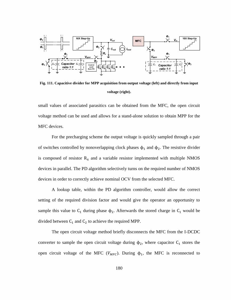
180
Fig. 111. Capacitive divider for MPP acquisition from output voltage (left) and directly from input
voltage (right).
small values of associated parasitics can be obtained from the MFC, the open circuit
voltage method can be used and allows for a stand-alone solution to obtain MPP for the
MFC devices.
For the precharging scheme the output voltage is quickly sampled through a pair
of switches controlled by nonoverlapping clock phases ϕ1 and ϕ2. The resistive divider
is composed of resistor Rx and a variable resistor implemented with multiple NMOS
devices in parallel. The PD algorithm selectively turns on the required number of NMOS
devices in order to correctly achieve nominal OCV from the selected MFC.
A lookup table, within the PD algorithm controller, would allow the correct
setting of the required division factor and would give the operator an opportunity to
sample this value to C1 during phase ϕ2. Afterwards the stored charge in C1 would be
divided between C1 and C2 to achieve the required MPP.
The open circuit voltage method briefly disconnects the MFC from the I-DCDC
converter to sample the open circuit voltage during ϕ2, where capacitor C1 stores the
open circuit voltage of the MFC (𝑉𝑀𝐹𝐶). During ϕ1, the MFC is reconnected to

181
converter, while the charge stored in C1 is again divided between both C1 and C2, to
achieve MPP.
Both methods can achieve accurate MPP for MFC, but the open circuit voltage
method is limited in the time constant value of the MFC’s 𝑅𝑀𝐹𝐶 and 𝐶𝑀𝐹𝐶 for it to reach
nominal 𝑉𝑀𝐹𝐶.
If the time constant is restrictively large, the capacitive divider would need to
disconnect the MFC from the I-DCDC converter for prohibitively large periods of time,
making it unsuitable for power harvesting from the MFC.
Once the MPP acquisition is completed, a comparator evaluates differences
between the desired reference and the input voltage for the CP (Vin). As the compared
voltages are DC values and Vin varies at a slower than a single comparator clock period,
the behavior can be approximated as continuous. The comparator topology implemented
[96] operates with a dedicated clock tuned at 100 kHz and characterized with a gain of
100 dB.
Charge pump and filter
The charge pump employed was that of a conventional current steering design
with a static current consumption of 100 nA. For the filter, a Type-II filter topology
commonly used in Phase-Locked Loops was realized due to the low power nature of the
system. The optimization of the control loop was mainly focused on improving
performance for the worst case MFC-L: RMFC of 8 kΩ and CMFC of 2.5 mF.

182
In order to improve phase margin under the already limited system parameters
offered by MFC-L, the zero frequency was placed at low frequencies, i.e., ~8 Hz. The
secondary pole, ωp2, was placed considering stability for the best case MFC (MFC-H).
Since GBP is much better than MFC-L, the only limitation was adequate phase margin.
The pole was positioned at ~80 kHz and improved both GBP and PM to 73.6
kHz and 45.7°, respectively. Values for the filter implemented were: R1= 20 kΩ, C1 = 1
μF, and C2= 10 pF; the filter was implemented with external components.
Current controlled oscillator
The current controlled oscillator (CCO) implemented for the MPPT scheme was
a wide tuning range and a three-stage ring oscillator topology [147]. The tuning range
was selected by the required frequency range for the SC input resistance (Fig. 106). The
implemented topology of the CCO offered a much broader linear range and only one
control voltage (𝑉𝑐) compared to the approach presented in [112], where control voltage
for both PMOS and NMOS in the transmission gate resistance had be considered. The
implemented CCO was designed for a linear tuning range (see (90)) from 10 kHz to 10
MHz with a gain of 10 MHz/V (𝐾𝑐𝑐𝑜) in order to cover the required values of 𝑓𝑠𝑤 for
impedance matching purposes.
10X step-up charge pump
Fig. 112 shows the DC-DC converter topology, where by monitoring the output
voltage the number of stages varies on load conditions. The implemented step-up
converter was composed of a 9-stage, 10X gain, 4-phase Dickson Charge Pump [57];

183
responsible for stepping up the MFC voltage to usable CMOS levels. This topology was
selected due to its inherent higher efficiency for lower power profiles [148, 149].
Fig. 112. 10X charge pump topology.
The switch design implemented a bootstrapped approach in order to minimize
Ron values throughout the entire converter. Fig. 113 shows the implemented technique
where each stage is activated via the Mx control bit. Both ΦA and ΦB were delivered
from a 4-phase nonoverlapping clock generator; previous and next stage block used the
remaining two phases for their own clock control. The bootstrapping effect through
phase 𝜙𝐴 precharges the capacitor 𝐶𝑏𝑡 to the voltage at the Vs node, then during 𝜙𝐵 and
additional potential is added to the bottom plate of 𝐶𝑏𝑡 of approximately 𝑉𝑜𝑢𝑡. This
allows for the overall overdrive voltage across the switching transistors to remain
constant throughout the entire step-up chain.
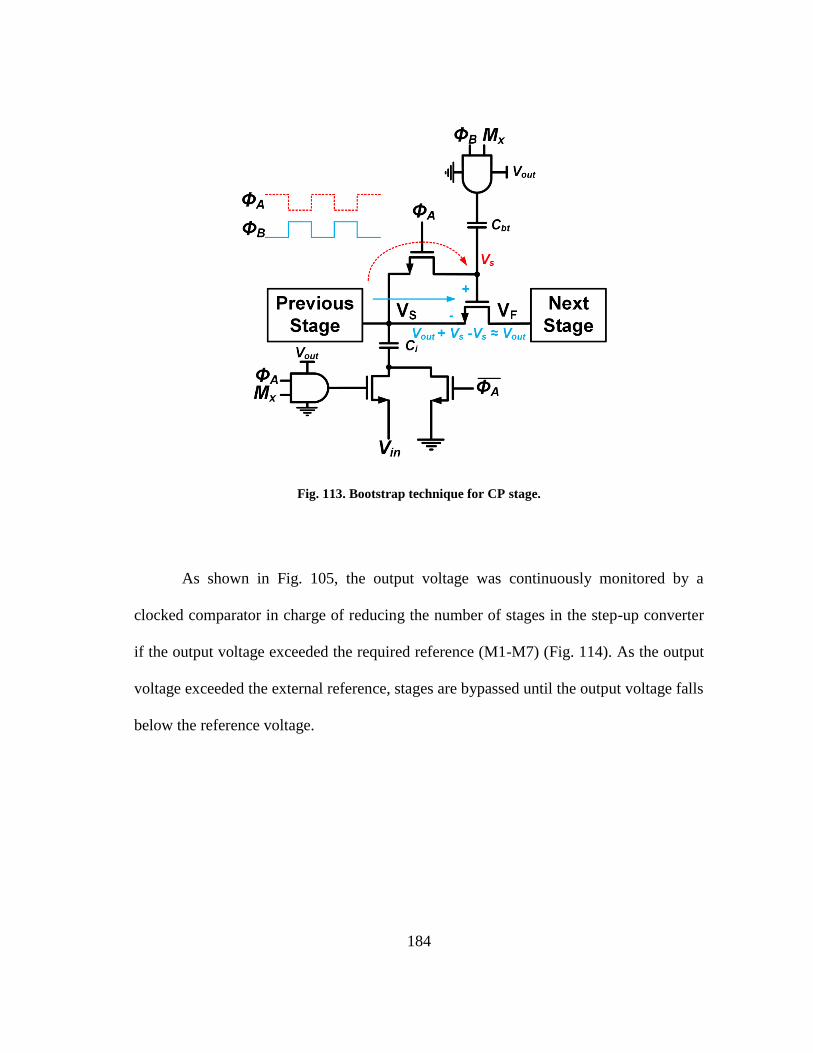
184
Fig. 113. Bootstrap technique for CP stage.
As shown in Fig. 105, the output voltage was continuously monitored by a
clocked comparator in charge of reducing the number of stages in the step-up converter
if the output voltage exceeded the required reference (M1-M7) (Fig. 114). As the output
voltage exceeded the external reference, stages are bypassed until the output voltage falls
below the reference voltage.

185
Fig. 114. Stage control block for output voltage monitoring.
Fig. 114 shows the overall structure of the Stage Control block. Only two stages
are permanently set in the power path due to the maximum voltage delivered by the
MFC, which is characterized to be 800 mV. If all programmable stages are bypassed and
the output voltage still exceeds the external voltage reference, the main oscillator clock
is disengaged, but maintains a secondary oscillator to drive both the MPP acquisition
block and Stage Control blocks (output and input comparators) of the PMU. The main
oscillator clock is re-engaged once the output voltage falls below the reference. By
extracting MPP during all operational up-time, regulation can be achieved as long as the
load does not demand more power than what is available at the input source; this is the
main limitation in all energy harvesting systems. Current demands within the system’s
capabilities will maintain the converter operating at MPP through the MPPT scheme,
sustaining the required output voltage.

186
I-DCDC system startup
The voltage delivered by the MFC does not allow for a self-starting operation
from the converter. An external one-time precharging of the output capacitor to 600 mV
is required to begin controller operation. Multiple different approaches may be taken to
start up the system [88, 124].
Once the system begins extracting energy from the MFC, there is no longer a
need for an external power source to power the I-DCDC.
Measurement results
The PMU system was fabricated in 0.18 μm CMOS process with an active area
of 1.8 mm2. Fig. 115 shows the die microphotograph of the PMU with the value for
output capacitor, 𝐶𝑜𝑢𝑡, being 100 mF.
Fig. 115. Die microphotograph of implemented I-DCDC and test bench.

187
For the MFCs, Fig. 116 shows the polarization curves for the 240 mL (MFC-L)
device obtained after eight months of operation, showing a maximum power output of
11.2 µW at a voltage of 300 mV (open circuit voltage of 600 mV). The maximum
power from the 1 L (MFC-H) device was 1.6 mW at a voltage of 400 mV (open circuit
voltage of 800 mV) (Fig. 14). This is in line with a typical two-chamber MFC power
performance when using wastewater inoculum and acetate as the carbon substrate. These
two MFCs were used to test how the developed I-DCDC performs at two different MFC
voltage and power levels.
Fig. 116. Power production of MFC-L (low power) and MFC-H (high power).

188
Maximum power point tracking
Fig. 117 shows correct MPPT extracted through the PMU by performing rapid
changes between the best and worst case condition MFC sources; both conditions
modified the operating point for MPPT (VMFC/2) as well as the pole location (ωp) for
the control loop. The change between MFCs was performed to simulate the effect of the
PD algorithm when selecting within the MFC array between ‘best’ and ‘worst’
conditions. The aforementioned variables were correctly dealt with by the PMU. As it
was calculated in section titled I-DCDC Implemented Circuit Blocks-Maximum Power
Point and Comparator Blocks, the GBP and PM for both cases was so drastically
different that settling time between MFC-H and MFC-L varied between ~100 ms for
MFC-H and ~3 s for MFC-L.
Fig. 117. The MPPT control loop correctly identifying MPP for extreme condition MFC-H and
MFC-L.

189
Voltage regulation
Fig. 118 shows output voltage regulation capabilities for the converter for 1.6
mW of input power and load current step from 100 μA to 400 μA and back. A 50 mV
drop at the output voltage is seen at 𝑉𝑜𝑢𝑡 as well as a 150 mV overshoot when load is
stepped down from 400 μA to 100 μA. The system is able to maintain regulation by
maintaining MPP throughout varying load current demands (extracting maximum power
from the source at all times). Whenever load current exceeds the input available power,
regulation cannot be maintained and the output voltage will drop.
Fig. 118. Output voltage load regulation test with load current variation for 1.6 mW of input power.
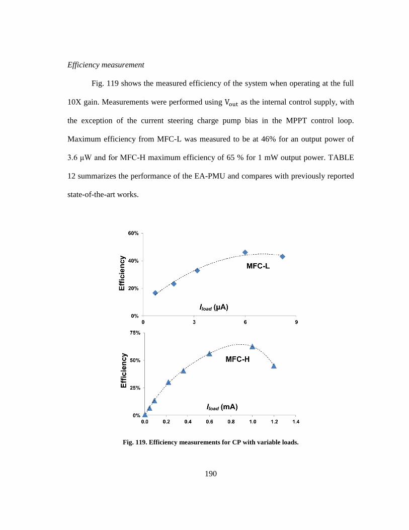
190
Efficiency measurement
Fig. 119 shows the measured efficiency of the system when operating at the full
10X gain. Measurements were performed using Vout as the internal control supply, with
the exception of the current steering charge pump bias in the MPPT control loop.
Maximum efficiency from MFC-L was measured to be at 46% for an output power of
3.6 μW and for MFC-H maximum efficiency of 65 % for 1 mW output power. TABLE
12 summarizes the performance of the EA-PMU and compares with previously reported
state-of-the-art works.
Fig. 119. Efficiency measurements for CP with variable loads.

191
Results from [42] show a higher efficiency due to lower number of stages in the charge
pump being used. The presented system is the only fully integrated PMU capable of
achieving both a broad range of matching and improved efficiency for energy harvesting
solutions operating below 1 V input voltage. Power consumption for the proposed I-
DCDC converter totals approximately 4.7 μW between static and dynamic power
consumed. It should be noted that higher power consumption was derived from the
increased number of stages of the I-DCDC.
Fig. 120. Power consumption for I-DCDC @ 1 MHz fsw (left) and 10 kHz fsw (right).
Fig. 120 breaks down the power consumed by dynamic and quiescent for 1 MHz
𝑓𝑠𝑤. Power consumption will automatically set depending on the power availability at
the input MFC source. With high MFC power profiles, the I-DCDC will require higher
𝑓𝑠𝑤 to achieve MPP, i.e., at 5 MHz the power consumption is 20 μW, but the power
extracted from the MFC was much higher.

192
TABLE 12. Summary of performance for MFC power management units.
SPECIFICATION [150] [42] [104] [136] [102] [151] THIS WORK
Input Voltage
Range 350 mV–480 mV 1V–5 V 315 mV 320 mV ~ 0.66 V > 0.6 V
300 mV-400 mV
@ MPP
Output Voltage 1.4 V 2 V ~ 1.1 V 5 V
1.8 V Charge
pump
3.3 V Boost
converter
0.9 V–
1.2 V 1.6 V–2 V
Power
Consumption 2.62 μW ‡
2.11 μW
@ 60 kHz
𝑓𝑠𝑤
NA NA NA
1 μW @
1 MHz
𝑓𝑠𝑤
933 nW @ 10 kHz
𝑓𝑠𝑤
36.4 μW @ 10
MHz 𝑓𝑠𝑤
MPPT No Yes Yes Yes No No Yes
Impedance
Matching Range - 100 kΩ NA NA - -
100 Ω–8 kΩ
(6.5 μF–2.5mF)
Input Source
Photovoltaic or
Thermoelectric
generator (TEG)
TEG MFC MFC MFC MFC MFC or TEG
Max. Efficiency 65% 58%
~ 90 % at 0.7
V output
voltage
45.21% 21.6%
85% at
0.9 V
output
voltage
64.88% with
MFC-HIGH at 1.8
V output voltage
Topology Charge Pump Charge
Pump
Boost
Converter
Boost
Converter
Charge
Pump and
Boost
Converter
Boost
Converte
r
Charge Pump
Technology 0.13 μm 0.35 μm Discrete Discrete Discrete 0.18 μm 0.18 μm
‡𝑓𝑠𝑤 for this power not reported

193
Conclusions
This chapter presents a fully integrated, I-DCDC converter for an EA-PMU
aimed at managing power of MFC arrays, through a time multiplexing harvesting
approach in order to overcome the voltage reversal issue in MFC arrays power
harvesting. MPPT and efficient DC step-up gain were performed through a FMS and
dynamic stage selection. It also showcases a novel MPPT design procedure, for
capacitive DC-DC converters and the stability considerations to be taken to achieve
MPP. The converter can achieve MPPT for a broad range of MFC power profiles,
ranging from 7.8 μW (𝑅𝑀𝐹𝐶 = 8𝑘Ω) to 1.6 mW (𝑅𝑀𝐹𝐶 = 100 Ω) as well as taking into
account parasitic capacitances from the MFCs (6 μF to 2.5 mF). The maximum
measured efficiency was of 65 % for 1.6 mW of input power and a 1 mA load current.

194
CHAPTER VI
AN AUTONOMOUS FULLY INTEGRATED ENERGY HARVESTING POWER
MANAGEMENT UNIT WITH DIGITAL REGULATION FOR IOT APPLICATIONS
Introduction
The research behind novel renewable energy sources has always been a critical
and major driving force in technological innovation. One of the breakthroughs in
renewable energy technologies has been the development of new and highly efficient
power management units (PMU) for energy harvesting (EH) systems. EH-PMUs are
focused on two major tasks: 1) Extract maximum power from the source, and 2) provide
a regulated output voltage. Major results have been accomplished for solar, kinetic, RF,
and thermoelectric sources [124, 152]. Advances in Internet of Things (IoT) devices
have allowed for complex and task specific solutions to become the new norm.
Complete PMUs are becoming a standard and the same can be seen in energy harvesting
[124, 152, 153]. The main challenges behind the design and implementation are the
stringent power constraints inherent in EH technology; for which dedicated PMU design
must overcome by becoming both low power, and high efficiency.
Providing both maximum power point tracking (MPPT), as well as output
voltage regulation is still an issue to be fully resolved. State-of-the-art solutions are
capable of performing maximum power point tracking and/or charging capabilities with
DC EH sources [154-156].

195
Nonetheless, delivering a regulated supply to a noise sensitive load (e.g. voltage
controlled oscillator) can potentially be an issue for current solutions. The need for a
PMU capable of performing both charging function, as well as load regulation, will
allow for a new set of functions for PMU with EH sources. These solutions can lead to
more robust IoTs and wireless sensor applications where efficiency and power storage
are critical for practical employment.
This chapter proposes an ultra-low power, fully integrated, autonomous PMU
capable of performing MPPT for dc EH sources, as well as performing both a charging
operation and output voltage regulation for noise sensitive blocks. The PMU is
comprised of a 10X step up charge pump with two-dimensional articulation for MPPT,
and a digital Low Dropout (LDO) regulator with input power sense capabilities. The
PMU does not require any additional external biasing or references, and can startup
autonomously with a minimum of 350 mV at the input of the converter. The proposed
PMU presents a solution for both the maximum power extraction from EH dc sources, as
well as offering both storage and regulation capabilities to different types of loads.
The chapter is divided up in the following sections: Section II presents the
overall proposed PMU with an overview of the main blocks comprising it, Section III
describes the building block implementation of the PMU, and Section IV discusses the
obtained measurements from a PMU prototype. Finally, Section V concludes the paper.

196
Fig. 121. Proposed block diagram of the power management unit.
Proposed power management unit
Fig. 121 shows the full system proposed for the PMU. The presented system is
comprised of 4 main blocks: 1) the startup block (system jump-start), 2) digital MPPT,
3) main converter (charge pump), and 4) the digital LDO. Each block of the PMU
requires no external references or external biasing in order for operation of the system.
With a fully enclosed operational capability, the proposed PMU can augment battery life
of wireless sensor systems; as well as deliver a regulated supply to sensitive systems,
e.g. voltage controlled oscillators. The system begins operation by sequentially enabling
each block depending on the availability of EH transducer power. A minimum of 350
mV is required to jump-start the system and begin preliminary power extraction through
the startup scheme.

197
A preset delay timer is designed into the startup scheme in order to assure
enough power is delivered to the storage capacitor. Once the timer runs out, the main
converter is engaged and startup disengaged. The main converter then begins the
harvesting operation along with step-up and maximum power extraction process. The
main converter steps up the dc EH transducer voltage to 2 V (𝑉𝑐ℎ𝑎𝑟𝑔𝑒), allowing for a
charging/storage operation at the output of the converter through 𝐶𝑐ℎ𝑎𝑟𝑔𝑒 . Once the 2 V
are achieved at the output of the converter, the digital LDO is activated to deliver a
regulated output voltage of 1.8 V through a secondary output node, 𝑉𝑜𝑢𝑡.
Startup block
The startup scheme is employed whenever there is no usable stored charge at the
𝑉𝑐ℎ𝑎𝑟𝑔𝑒 node. This would require the converter to begin operation from whatever power
the harvesting source can deliver, which can vary significantly over a wide range of
values. To circumvent the low voltage nature of the energy harvesting sources used, and
enable autonomous operation of the PMU, the startup block shown in Fig. 122 is
included to jump-start the PMU to being operation. The startup block is composed of a
Dickson-based charge pump with a 3X voltage gain and a dedicated low frequency
voltage controlled ring oscillator (VCO), as well as an Enable timer block which enables
the main converter + digital LDO blocks while disengaging the startup block.

198
Fig. 122. Startup scheme generating a supply rail for the main converter to begin operation.
Main converter charge pump
Once the hand-off between the startup block and main converter is enabled, the
main converter takes over and begins the primary harvesting effort for the PMU.
Powered from the 𝑉𝑐ℎ𝑎𝑟𝑔𝑒 node, the main DC-DC converter in the PMU begins
maximum power extraction from the EH source. The main converter topology is a 9-
stage, step-up converter, based on a Dickson charge pump topology [41]. The converter
manages maximum power extraction for the system by implementing a digital maximum
power point tracking (DMPPT) scheme via a frequency modulation (FM) through a
digitally controlled oscillator (DCO).

199
Fig. 123. Digital maximum power point tracking with maximum power point acquisition block for
main converter.
The DMPPT, Fig. 123, scheme allows the converter to harvest the highest energy
from dc EH sources, by modulating the current being drawn by the PMU to reach
maximum power extraction conditions through varying the switching frequency, 𝑓𝑠𝑤, of
the main converter. The converter also possesses individual control over the 9-stages
involved in the step-up process (Fig. 124); this control permits the system to bypass any
unnecessary step-up stages to reach the goal voltage. Thus, the two functions of the main
converter are summarized as: extract maximum power from the EH source, and to step-
up the input voltage from the EH source to 2 V. The main converter has an internal
voltage reference powered directly from 𝑉𝑐ℎ𝑎𝑟𝑔𝑒, permitting the system to operate
autonomously. Section III-B and C further describe the system implementation.

200
Fig. 124. Main converter (10x) showing bypassing capabilities through stage control block.
Low power digital LDO
Among the chief concerns with power converters focused on EH technology, are
the regulation capabilities of a harvesting system. Efforts have been mainly focused on
maximum power extraction for storage/charging applications [150, 157, 158], and while
there are a few solutions that offer voltage regulation [8, 42, 159], they still require
external references and/or external inductors to implement. The proposed approach with
the PMU implements the regulation block through a digital LDO, shown in Fig. 125,
capable of adapting the pass-device through two main control means: a coarse tuning
method that selects the pass-device array to maximize efficiency, and a fine tuning
method to regulate the output voltage to the required reference.

201
The pass-device fragmentation (fine tuning) is a common practice and has shown
positive results for sub-micron processes [79, 160], but for EH solutions the variability
of the input sources power may limit delivered power to the output load. By utilizing the
power density information from the main converter and DMPPT blocks a coarse tuning
approach is implemented, which selects a pass-device array from a device bank,
according to the available power from the EH source. Three main array banks were
implemented which can handle 10s of μWs to 10s of mWs in power range to maximize
efficiency by reducing switching losses inherent in larger device geometries. The digital
LDO requires no additional external references or biases; it directly draws power from
the 𝑉𝑐ℎ𝑎𝑟𝑔𝑒 node for all of the block’s needs. This allows for a fully autonomous
operation from the digital LDO. The next section describes the design implementation in
further detail.

202
Fig. 125. Digital LDO regulation scheme.
Circuit block implementation
The proposed PMU presents a dc energy harvester with the capability for full
autonomous operation. The system has the potential of being deployed along with
remote sensor nodes to enhance and extend battery lifetime of the device. The present
section elaborates on the PMU block implementations.
Startup block
The startup block enables operation from voltages down to 350 mV, Fig. 126.
The entire startup scheme is powered directly from the harvesting source’s open circuit
voltage, and once the VCO starts, it drives a 4-phase non-overlapping clock for the 3X

203
charge pump. A dedicated counter sets a time limit on the startup by dividing the VCO
startup switching frequency (fsw) by 222
(fsw/222
). Operating at 350 mV, the startup VCO
delivers a fsw of ~75 kHz, for a roughly 1 minute-long starting-up time. This ensures that
the startup build up a high enough voltage for the main DC-DC converter for proper
operation. The startup block ends up delivering ~650 mV for the main DC-DC
converter, at the 𝑉𝑐ℎ𝑎𝑟𝑔𝑒 node.
Once the main converter begins harvesting energy from the dc source, the startup
circuit is disengaged and does not become operational again until the entire system is
shut down and reset through complete power deprivation. A set timer of ~ 1 minute was
set as variable conditions on EH sources may allow the system to operate under non-
optimal conditions, i.e. extreme low power availability. Although the startup block is set
to a 1 minute hold period for the PMU to hand-off to the main converter, this can
potentially be modified to a lower hold period through bypassing several clock dividers
Fig. 126. Startup scheme clock generation and enable timer block.

204
depending on availability of power from the EH source. Furthermore, since the startup
scheme is only operational during initial system settling it is a one-time operational
block, and does not negatively impact the overall performance if a steady EH source is
present.
Digital maximum power point tracking
In order to extract maximum power from the EH source a MPPT scheme must be
set to guarantee this. Depending on the type of EH source, maximum power can be
achieved through a resistive matching or/and through power detection algorithms [161,
162]. Both schemes can be implemented in a variety of ways ranging in complexity and
power consumption [8, 163, 164]. The DMPPT is implemented to assure the converter
extract maximum power, Fig. 123 presents the components comprising the DMPPT:
dynamic comparator, up/down counter, decoder, and DCO. Fig. 127 also shows the MPP
acquisition block used to obtain the reference for the DMPPT, 𝑉𝑀𝑃𝑃 .
The overall function of the DMPPT is to drive the 𝑉𝑖𝑛 node to match the 𝑉𝑀𝑃𝑃
reference by increasing/decreasing the switching frequency of the main converter
through the use of the up/down counter and decoder to set the switching frequency of the
DCO. The 𝑉𝑀𝑃𝑃 reference sets the MPP for the EH sources and is divided into 3
different operating modes: for thermoelectric generators (TEG), for solar cells (SC), and
for microbial fuel cell (MFC) sources.

205
Fig. 127. Maximum power point acquisition scheme for difference dc EH sources a) thermoelectric
generators, b) PV solar cells, c) Microbial fuel cells (MFCs), and d) the timing diagrams for both
switching phases.
Fig. 127 presents the 3 varying methods with which the 𝑉𝑀𝑃𝑃 for the needed EH
source is achieved. Fig. 127a illustrates the manner in which harvesting efforts with
TEGs the DMPPT samples the open circuit voltage and divides it by two using a
capacitive voltage divider to set the maximum power point (MPP) condition for the
PMU:
𝑉𝑀𝑃𝑃 = 𝑉𝑂𝐶𝑉 (
𝑅𝑇𝐸𝐺
𝑅𝑇𝐸𝐺 + 𝑅𝑖𝑛) =
𝑉𝑂𝐶𝑉
2
(96)
Once the 𝑉𝑀𝑃𝑃 value is correctly obtained, the input voltage of the converter, 𝑉𝑖𝑛,
is driven to match the MPP condition.

206
For the SCs, an additional capacitor, 𝐶𝑃𝑉, is placed next to 𝐶1 (Fig. 127b) to
increase the effective value of 𝐶1 and set the maximum power condition to 70-80% of
the open circuit voltage (OCV) (VMPP = 70-80% VOCV) [163, 164], approximate MPP
condition for SCs. The capacitive divider approach, while not as accurate as other MPP
algorithms, is a straightforward implementation and is lower in power consumption. This
lends itself for small solar cell dimensions for which the MPP algorithm is accurate (no
partial shading conditions). For the MFCs, a biomass power generation systems [165]
(Fig. 127c), a resistor ratio is placed on 𝑉𝑐ℎ𝑎𝑟𝑔𝑒 and the value of 𝑉𝑀𝑃𝑃 is set to OCV
divided by two:
𝑉𝑀𝑃𝑃 = 𝑉𝐶ℎ𝑎𝑟𝑔𝑒 (
𝑅𝑇𝑢𝑛𝑒
𝑅𝑋 + 𝑅𝑇𝑢𝑛𝑒) =
𝑉𝑂𝐶𝑉
2
(97)
The same method used by the TEG sources would not properly achieve MPP due
to the internal parasitic capacitance of the source, requiring long times (Φ2 >> Φ1) of
sampling to correctly reach OCV [165] (Fig. 127d), making both sampling capacitors
and input capacitor connected at Vin prohibitively large. The clock periods shown in Fig.
127d are set by a dedicated oscillator, 𝑓𝑐𝑜𝑚𝑝, free running at ~100 kHz, this sets the
sampling times for 𝜙1 and 𝜙2 to 𝑇𝑐𝑜𝑚𝑝/10 and 𝑇𝑐𝑜𝑚𝑝 respectively. The low frequency
sampling of the OCV voltage (~ 1μs), assures that the EH source is only briefly
disconnected from the PMU and the sampled OCV voltage value is refreshed in the
sampling capacitors.
Once the reference, 𝑉𝑀𝑃𝑃, is correctly obtained, the dynamic comparator speeds
up or slows down the DCO through an up/down counter with decoded thermometric

207
output to modulate the input resistance of the main converter to achieve maximum
power transfer. The input resistance of the capacitive DC-DC converter is approximated
as:
𝑅𝑖𝑛 =
𝑉𝑖𝑛
𝐼𝑖𝑛=
𝛼 𝐶𝑖 𝑓𝑠𝑤 𝑁 𝑅𝑐ℎ𝑎𝑟𝑔𝑒 + (𝑁 + 1) 𝐴𝑉
𝛼 𝐶𝑖 𝑓𝑠𝑤 𝑁 (𝑁 + 1) 𝐴𝑉
(98)
where the variables in 𝛼, 𝑅𝑐ℎ𝑎𝑟𝑔𝑒, 𝑁, 𝐶𝑖, 𝑓𝑠𝑤, and 𝐴𝑉 are the ratio of parasitic
capacitance to stage capacitance, charging equivalent resistance (𝑉𝑐ℎ𝑎𝑟𝑔𝑒/𝐼𝑐ℎ𝑎𝑟𝑔𝑒) seen
at 𝐶𝑐ℎ𝑎𝑟𝑔𝑒, number of stages, capacitance per stage, switching frequency of the
converter, and the voltage gain for the charge pump given by:
𝐴𝑉 = (𝑁 + 1) ∙ (1
1 +𝑁
𝐶𝑖 𝑓𝑠𝑤 𝑅𝐿𝑜𝑎𝑑
) (99)
The expression (98) sets the limits for which input resistance can be varied
through both number of stages in the converter, voltage gain, and switching frequency.
For the main converter design, emphasis was placed on switching frequency as main
control method to accurately achieve a wide range of MPPs. The FMS implements a
DCO with wide operating range to correctly extract maximum power from most EH
sources. The DCO provides rail to rail oscillation and uses a coarse (capacitive) and fine
(resistor) tuning schemes to vary switching frequency through a CMOS inverter delay
cell configuration, Fig. 128. A digital word of 8 bits (FF in hexadecimal) is used to tune
both capacitor and resistor banks to achieve the correct value for 𝑓𝑠𝑤 at MPP. The
capacitor bank unit cell value for 𝐶𝐷 is ~2 pF, and the resistor bank unit cell value for

208
𝑅𝐷 is ~ 10 kΩ. Careful attention is spent on layout efforts to minimize mismatch
between resistor and capacitors within their respective bank values.
Fig. 129 the varying switching frequency achieved with different DCO code
values in hexadecimal format, XY h, with X values signifying the capacitor bank code,
and Y the resistor bank code. The output of the DCO is then sent to the 4-phase non-
overlapping clock generator to later transmit to the main converter switches.
Fig. 128. Digital controlled oscillator implementation for DMPPT.
With the varying frequency and variable number of stages of the main converter,
the input resistance, 𝑅𝑖𝑛, of the PMU can effectively be adapted to achieve the required
input voltage condition (𝑉𝑖𝑛) to meet MPP (𝑉𝑖𝑛 = 𝑉𝑀𝑃𝑃). Fig. 130a shows the range
over which the 𝑅𝑖𝑛 of the PMU is tuned over switching frequency and charge pump
number of stages to meet the MPP condition.

209
Notice how 𝑅𝑖𝑛 is inversely proportional to high values of 𝑓𝑠𝑤 and number of
stages. This sets the limit over which the MPP condition can be met by the PMU; for
high values of dc gain from the PMU (low input voltage EH source) more stages will be
required to achieve the goal output voltage of 2 V, limiting the resistance range over
which MPP can be met.
Fig. 129. Digitally controlled oscillator frequency range and code word in hexadecimal format.
For lower values of dc gain (high input voltage EH source), the number of stages
can be decreased and the range over which the 𝑅𝑖𝑛 of the PMU can change increases at
the cost of higher valued 𝑓𝑠𝑤 to meet lower resistance values. A second variable to
consider is the output voltage value, 𝑉𝑐ℎ𝑎𝑟𝑔𝑒, Fig. 130b shows how output voltage values
also affect 𝑅𝑖𝑛. Differences between 1 stage and 9 stage implementations show the

210
limitation of values for 𝑅𝑖𝑛 for which the PMU can achieve. All three variables, 𝑓𝑠𝑤,
output voltage, and number of stages, must be considered when designing a MPPT
scheme for a charge pump, these variables are the inherent limitation on the topology
over which 𝑅𝑖𝑛 values can be accomplished.
Fig. 130. Input resistance range capabilities for proposed PMU with a) varying charge pumps stages
v. fsw and b) varying output voltages v. fsw.
Fig. 131. Full schematic of 10X main converter with variable stage selection.

211
Main converter charge pump
The main converter charge pump is comprised of 9 step-up stages to achieve the
required output voltage at the output of the converter. The number of stages are not fixed
and allow for increasing/decreasing depending on the voltage delivered by the EH
source. Fig. 131 shows the full schematic of the step-up main converter. Each individual
stage, +1 Step-up Stage, receives both its clock signals from the DCO and stage
enabling/disabling signals from the Stage Control block.
The switch design implemented a bootstrapped approach in order to minimize
𝑅𝑜𝑛 values throughout the entire converter, where each stage is activated via the 𝑇1−8
control bits. Both 𝜙1𝐴,𝐵 and 𝜙2𝐴,𝐵 (Fig. 131) are delivered from the 4-phase non-
overlapping clock generator. The bootstrapping effect through phase 𝜙2𝐴,𝐵 precharges
the capacitor 𝐶𝑏𝑡 to the voltage stored in capacitors 𝐶𝑖, then during 𝜙1𝐴,𝐵 and additional
potential is added to the bottom plate of 𝐶𝑏𝑡 of approximately 𝑉𝑐ℎ𝑎𝑟𝑔𝑒. This allows for
the overdrive voltage across the switching transistors to remain constant throughout the
entire step-up chain.
As mentioned previously, the main converter has a variable stage control in order
to reduce the number of stages 𝑇1−8 when high enough voltage is available from the
harvesting sources. Stages can potentially be reduced to a minimum of one when the
input voltage provided from the EH source is 1V. The Stage Control block is shown in
Fig. 132 comprised of a CMOS reference, capacitive divider, comparator, counter, and
decoder. The reference implemented is a CMOS subthreshold reference [166], powered
directly from 𝑉𝐶ℎ𝑎𝑟𝑔𝑒 node delivering a voltage of approximately 200 mV with a power

212
consumption of ~7 μWs for 2 V at the 𝑉𝑐ℎ𝑎𝑟𝑔𝑒 node. The capacitive divider performs a
series-parallel step-down operation, with the same clock phases used in the MPP
acquisition block, to obtain the 𝑉𝐷𝑖𝑣/10 voltage (𝑉𝐷𝑖𝑣/10 = 𝑉𝑐ℎ𝑎𝑟𝑔𝑒/10); this voltage is
used in the Stage Control loop to add or reduce stages in the main converter by
triggering the comparator high or low, thus increasing or reducing the up/down counter.
The counter output is then sent to the decoder block, which performs the
enabling/disabling operation of the main converter (Fig. 124).
Fig. 132. Stage control block with low power reference schematic.
With each additional stage added to the main converter, efficiency decays. So the
addition of more stages to the main converter comes at a price on overall system
efficiency. From [167] the efficiency expression (5) shows the relationship between
number of stages (N), switching frequency, (𝑓𝑠𝑤 ), ideal voltage gain (𝐴𝐼𝑑𝑒𝑎𝑙 = 𝑁 + 1),
and ratio of stage and parasitic capacitances (𝛼):

213
𝜂 =
𝐴𝑉
(𝐴𝐼𝑑𝑒𝑎𝑙) + 𝛼 𝑁2
(𝐴𝐼𝑑𝑒𝑎𝑙) − 𝐴𝑉
(100)
From (100) each additional stage increase (N), increases the value of the second
term in the denominator and reduces the overall efficiency of the system. As stated in
[42], efficiency limitations on capacitive DC-DC converter are heavily driven by 𝛼 ratio
inherent in the process. This shows the intrinsic limitations with any capacitive DC-DC
converter and viability of implementation with each process.
Digital low dropout regulator
Regulation is among the key building block for any system which requires a
regulated supply voltage to supply noise-sensitive blocks [168]. The implemented digital
LDO allows for a regulated output voltage through an energy aware scheme which
emphasizes overall efficiency by minimizing switching losses in the switched pass
device. As previously mentioned in Section II, there are two main variables that allow
for efficient regulation in the PMU: the power array selector loop, and the load feedback
loop information.
Since with any EH system power is limited to what is available from the source,
so having a one-size fits all solution can limit the range of applications over which the
system can be applied to. The implemented digital LDO takes power level information
from the DMPPT block and Stage Control Block, Fig. 133, and selects the best suited
PMOS pass device to deal with load demand, while minimizing power consumption
required in driving the device.

214
The load feedback loop performs the required fine tuning of the pass device once
the best suited array is selected. Each array is broken up into multiple individually driven
pass devices which comprise the equivalent full pass device. It is this load feedback loop
which performs the required control for load regulation.
Fig. 133. LDO pass device array selector.
Fig. 134 presents the digital LDO structure; comprised of a resistive divider,
comparator, counter, decoder, and 3 banks of pass device arrays. The decision to
implement a resistive divider for the LDO instead of a capacitive divider is due to the
need for a steady and ripple-free supply. This produces a quiescent current being
consumed (~80 nA), but allows the generation of the LDO voltage reference, 𝑉𝑟𝑒𝑓.
TABLE 13 shows the combination, of both DCO code and number of stages from the
main converter (N), which enable the LDO pass device arrays as well as the equivalent
input power coming in from the EH source.

215
It should be noted that for high values of 𝑓𝑠𝑤, the number of stages are irrelevant
due to the high detected power profile from the DMPPT (low 𝑅𝐼𝑁).
The voltage regulation loop continuously compares the output voltage, 𝑉𝑜𝑢𝑡, with
𝑉𝑟𝑒𝑓, depending on load current demand 𝑉𝑜𝑢𝑡 may exceed or go below 𝑉𝑟𝑒𝑓, this triggers
the comparator high or low which in turn increases/decreases the 5-bit counter, leading
to an increase or decrease in the number of individually driven
Fig. 134. Digital LDO implementation.
devices by the decoder. The digital LDO structure possesses a dedicated clock free
running at ~ 1 MHz, 𝑓𝐿𝐷𝑂. Each array is divided up into 32 separate transistor fingers
which are individually enabled through a load feedback loop.
VCharge
2.2 MΩ
(RB1)
22 MΩ
(RB2)
Low
power
PMOS
array
Medium
power
PMOS
array
High
power
PMOS
array
VCharge
ILoad
Power Array Selector
Loop (DMPPT)
Cout
5 bit Up/Down
counter
Vout
Vref
32 bits
fLDO
Vout
Cfilter
Decoder

216
Where
𝑉𝑟𝑒𝑓 =
𝑉𝑐ℎ𝑎𝑟𝑔𝑒 𝑅𝐵2
𝑅𝐵2 + 𝑅𝐵1
(101)
Thus;
𝑉𝑜𝑢𝑡 =
𝑉𝑐ℎ𝑎𝑟𝑔𝑒
1 +𝑅𝐵1
𝑅𝐵2
(102)
TABLE 13. Power detection logic parameters for LDO array selector.
POWER
SPECIFICATION
DCO CODE
NUMBER OF STAGES
(MAIN CONVERTER)
INPUT POWER LEVEL
High Power Array 0H-FH ALL STAGES From 250 μW to 2 mW
Mid Power Array
30H-3FH
10H-1FH
3-5 STAGES From 50 μW to 249 μW
Low Power Array
F0H-FFH
70H-7FH
6-9 STAGES From 12 μW to 49 μW
As with any regulator, efficiency is crucial in the design of the PMU. This
becomes even more so in EH systems. Due to the switching nature of the digital LDO,
efficiency calculations were performed to set the ideal size for the pass device of the
regulator, for the power levels expected at the input of the PMU. Fig. 134 shows the
equivalent model of the digital LDO.

217
As shown in (2), each transistor array is sized to handle a particular power
domain (Low, Mid, and High), that is available from the EH source.
𝑊
𝐿 𝐴𝑟𝑟𝑎𝑦=
2𝐼𝑙𝑜𝑎𝑑
𝑉𝑑𝑟𝑜𝑝𝐾𝑝(𝑉𝑐ℎ𝑎𝑟𝑔𝑒 − 𝑉𝑡)
(103)
Following the power ranges from TABLE 13, transistor array sizes were
determined to maintain the 200 mV drop (𝑉𝑑𝑟𝑜𝑝) and expected load current for said
power domain. Finally the arrays were divided up into the 32 segments for each array to
be individually controlled by a 5 bit decoder. The sizing allows a reduction in switching
losses associated with the transistor capacitances, thus improving efficiency for a power
limited system without the need of a more complex digital controller.
Measurement results
The PMU was design and implemented in 180 nm CMOS process. Fig. 135
shows the prototype converter PCB and die photo. The PCB dimensions are 3cm x 3cm,
and die has 2 mm x 2mm dimensions. The PMU works for input voltages (once startup
sequence has run its course) ranging from 250 mV to 1.1 V for the main converter. The
storage capacitor 𝐶𝑐ℎ𝑎𝑟𝑔𝑒, was set at 1 mF, and output capacitor (output of digital LDO)
set at 10 μF. The external capacitors used for MPP acquisition are set at 100 pF, 100 pF
and 33 nF for 𝐶1, 𝐶2, and 𝐶𝑃𝑉 respectively. The capacitive divider for the Stage Control
block was performed with 10 μF external capacitors. Finally, the resistive divider for the
digital LDO control loop was implemented with 2 external resistors of 2.2 MΩ and 22
MΩ to set the reference. 𝑉𝑅𝐸𝐹, at 1.8 V.
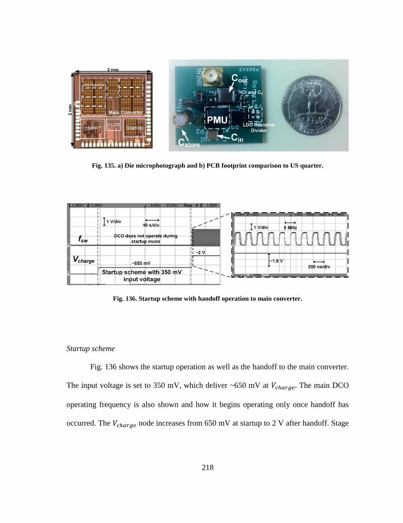
218
Fig. 135. a) Die microphotograph and b) PCB footprint comparison to US quarter.
Fig. 136. Startup scheme with handoff operation to main converter.
Startup scheme
Fig. 136 shows the startup operation as well as the handoff to the main converter.
The input voltage is set to 350 mV, which deliver ~650 mV at 𝑉𝑐ℎ𝑎𝑟𝑔𝑒. The main DCO
operating frequency is also shown and how it begins operating only once handoff has
occurred. The 𝑉𝑐ℎ𝑎𝑟𝑔𝑒 node increases from 650 mV at startup to 2 V after handoff. Stage

219
control is also shown in Fig. 136, highlighting the stage decrease to meet the required
output voltage, no load conditions were set for this test.
Digital maximum power point tracking
Multiple tests were performed on the PMU to surmise MPPT efficiency with the
different EH sources. Fig. 137 shows the MPPT efficiency of the presented PMU. As
expected, the OCV method proves reliable for both MFC and TEG sources, with >95 %
tracking efficiency for input powers < 100 μWs. The error at higher input powers
translates to lower internal resistances from the MFC and TEG sources; hence, higher
switching frequencies are required from the DCO. As can be seen from Fig. 137, the
resolution for switching frequencies is diminished at higher frequencies, causing the
error in MPPT tracking efficiency.
The results for the SC source show a lower MPPT efficiency, maximum at 87%;
this is due to the nonlinear nature of the SC source, and the implementation of the OCV
method. Although the MPPT efficiency is lower than previously reported literature, the
overall control power consumption + capacitive divider is minimal when compared
(~580 nW) to other reported works [159, 169].

220
Fig. 137. Digital maximum power point tracking efficiency for MFC, TEG, and PV solar cells.
Fig. 138. Digital low-dropout regulator load regulation test for 1.75 mW of input power and a 900
μA step load current.

221
Voltage regulation (digital LDO)
Fig. 138 shows the load test response of the system for a step of ~900 μA.
Output voltage (𝑉𝑜𝑢𝑡) is regulated at 1.8 V from the 2 V stored at 𝑉𝑐ℎ𝑎𝑟𝑔𝑒. A maximum
voltage overshoot of 55 mV can be seen, with a settling time of ~ 1 ms for both step
cases.
Wireless sensor node temperature sensor testing
Additional tests of the PMU powering a wireless sensor were also performed to
showcase the PMU’s power delivering capabilities. The PMU was powered by Laird
Technologies thermoelectric module, showing a 550 mV OCV and equivalent internal
resistance of ~10 Ω (𝑃𝑖𝑛 = 30 𝑚𝑊).
Fig. 139. Internet of Things (IoT) testing configuration A) illustration of power management unit
with temperature sensor and B) unfolded implementation for IoT configuration with thermoelectric
generator unit.

222
Fig. 140. Wireless sensor node testing voltage profile A) with 1F supercapacitor at Cstore and B)
temperature sensor transmitted results.
A 1 F supercapacitor was placed as 𝐶𝑠𝑡𝑜𝑟𝑒 for the testing procedures, and the
wireless sensor used was a Monnit Wireless Temperature Sensor [170]. Fig. 139A shows
an illustration of the implemented PMU with sensor node, and Fig. 139B shows the
implemented sensor with PMU in an unfolded configuration as well as the utilized TEG
unit.
The sensor was powered with an operating voltage of ~2 V at 𝑉𝑐ℎ𝑎𝑟𝑔𝑒 (900 MHz
operating frequency for wireless transmission). Power of 85 mW is consumed during
each sense and transmit event. Fig. 140 shows A) the voltage charging profile at 𝑉𝑐ℎ𝑎𝑟𝑔𝑒,
as well as the input voltage through the startup, MPPT, and 2 V output voltage setting;
B) shows the registered temperature transmitted by the sensor.
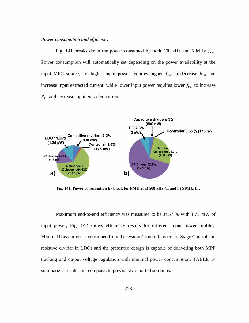
223
Power consumption and efficiency
Fig. 141 breaks down the power consumed by both 500 kHz and 5 MHz 𝑓𝑠𝑤.
Power consumption will automatically set depending on the power availability at the
input MFC source, i.e. higher input power requires higher 𝑓𝑠𝑤 to decrease 𝑅𝑖𝑛 and
increase input extracted current, while lower input power requires lower 𝑓𝑠𝑤 to increase
𝑅𝑖𝑛 and decrease input extracted current.
Fig. 141. Power consumption by block for PMU at a) 500 kHz fsw and b) 5 MHz fsw.
Maximum end-to-end efficiency was measured to be at 57 % with 1.75 mW of
input power, Fig. 142 shows efficiency results for different input power profiles.
Minimal bias current is consumed from the system (from reference for Stage Control and
resistive divider in LDO) and the presented design is capable of delivering both MPP
tracking and output voltage regulation with minimal power consumption. TABLE 14
summarizes results and compares to previously reported solutions.
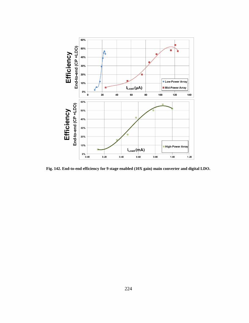
224
Fig. 142. End-to-end efficiency for 9 stage enabled (10X gain) main converter and digital LDO.

225
TABLE 14. Performance summary
SPECIFICATION [150] [42] [171] THIS WORK
Input Voltage
Range 350 mV– 480 mV 1 V – 5 V 320 mV – 600 mV
250 mV – 1.1 V
(for main converter)
Output Voltage 1.4 V (regulated) 2 V (un-regulated)
1.508 V (regulated)
2.04 V – 3.7 V
(un-regulated)
2 V (un-regulated)
1.8 V (regulated)
Power
Consumption 3 µW (Quiescent only)
2.11 μW (Controller only
Driver power not included)
Not reported (startup scheme
only)
1.18 μW controller @ 500 kHz 𝑓𝑠𝑤
11 μW with driver power consumption @
500 kHz 𝑓𝑠𝑤
Startup
270 mV (unregulated output
voltage)
400 mV (regulated output
voltage)
- 320 mV 350 mV
(regulated output voltage)
MPPT No Yes No Yes
Autonomous Yes No Yes Yes
Impedance
Matching Range NA 100 kΩ NA
>300 kΩ to <10 Ω
(discrete steps)
Regulation No Yes (external reference) No Yes @ 1.8 V
Input Source Solar Cell/ Thermoelectric
generator (TEG) TEG
Microbial Fuel Cells
(MFC)/TEG/Solar Cells MFC/TEG/Solar Cells
Max. Efficiency 65%
(for 4 stage CP)
82%
(For 1 stage charge pump)
89% (capacitive load, no
current demand)
90% w/o regulation
(1 Stage for Charge Pump)
81% w/D-LDO
(1 Stage for Charge Pump)
Technology 0.13 μm 0.35 μm 0.18 μm 0.18 μm

226
Conclusions
This chapter presents a PMU able to perform startup operation, maximum power
extraction for DC type EH sources (solar, thermal, biomass), and deliver a regulated
output voltage through a digital LDO regulator, presenting a solution to the regulation
and maximum power extraction dilemma present in current PMU solutions aimed at EH
sources. The PMU operates in a complete autonomous fashion, with charging/regulation
capabilities with minimum power consumption, and allows operation from voltages as
low as 350 mV through the startup block. Maximum power extraction is performed
through a fully digital MPPT scheme, allowing for minimal quiescent consumption with
minimum power overhead cost. Information about the source-power density availability
from the DMPPT and number of stages implemented from the Stage Control is passed
on to the digital LDO, which uses this information to increase or decrease the pass
transistor size. This allows for an overall power consumption decrease by reducing the
gate driving losses associated with large pass transistor devices and enhance efficiency
while delivering a regulated voltage to noise sensitive blocks. The PMU possesses the
capability of internal reference generation through capacitive, and resistive dividers, as
well as an internal voltage reference allowing for true autonomous operation. The system
was fabricated in 180 nm CMOS process and maximum end-to-end efficiency was
measured to be at 57 % with 1.75 mW of input power

227
CHAPTER VIII
SUMMARY AND FUTURE WORK
The design and implementation of inductive, capacitive and linear regulators for
energy harvesting technology has been presented. Solutions for thermoelectric
generators, microbial fuel cells, and photovoltaic energy harvesting sources have been
fabricated and tested.
Chapter III showed a solution for a thermoelectric generator array intended for
medical applications. The implemented inductive switching regulator is capable of
achieving maximum power transfer through a frequency modulation tracking loop, while
maintaining high efficiency through a Pseudo-Zero Current Switching scheme. Results
obtained show comparable to state-of-the-art solutions with a wider matching range by
the presented regulator.
Chapter IV showed a solution for microbial fuel cells through a self-powered,
inductive switching regulator. A new maximum power point tracking scheme was
implemented in order to manage the internal parasitic capacitance of the fuel cell and
correctly achieve matching between the fuel cell and regulator. A true Zero Current
Switching scheme is also implemented to enhance overall efficiency of the solution by
over 40% compared to the results obtained from the proposed PMU in chapter III.
Chapter V presents a capacitive switching regulator capable of handling arrays of
microbial fuel cells or thermoelectric generators. The regulator utilizes a frequency
modulation control in order to match the internal impedance of the fuel cells with its
own internal impedance to ensure maximum power transfer. The regulator also

228
possesses a programmable stage control to allow for a level of output voltage regulation
while maintaining minimum power consumption. Overall results show comparable
results to state-of-the-art solutions, with improved matching and power extraction
dynamics.
Finally, chapter VI presents a fully autonomous, capacitive switching regulator
with a digital Low Dropout regulator for a full power management unit aimed at Internet
of Things applications. The capacitive regulator is capable of performing maximum
power transfer from any DC type energy harvesting sources. The power management
unit also performs a start-up operation without the need of additional power from
batteries or charged capacitors. Regulation is performed by communication between the
main regulator and dropout regulator in order to enhance pass device size, thus
improving power efficiency.
The common denominator is the need for further research into simultaneous
multiple input energy harvesting regulators can be potentially explored to present a truly
stand-alone solution capable of dealing with multiple availability conditions of the
energy harvesting transducers. This multiple source harvesting implementation is
recommended if energy harvesting is to be adopted by mainstream applications.

229
REFERENCES
[1] H. Rahimi-Eichi, U. Ojha, F. Baronti, and M. Chow, "Battery Management
System: An Overview of Its Application in the Smart Grid and Electric
Vehicles," IEEE Industrial Electronics Magazine, vol. 7, pp. 4-16, 2013.
[2] M. Guarnieri, "When Cars Went Electric, Part 2 [Historical]," IEEE Industrial
Electronics Magazine, vol. 5, pp. 46-53, 2011.
[3] K. Fehrenbacher. (2010). Dear Friedman: There is no Moore's Law for Batteries
[online]. Available: https://gigaom.com/2010/09/27/dear-friedman-there-is-no-
moores-law-for-batteries/
[4] A. Valenzuela, "Energy Harvesting for No-Power Embedded Systems," ed:
Texas Instruments, 2008.
[5] R. J. M. Vullers, R. V. Schaijk, H. J. Visser, J. Penders, and C. V. Hoof, "Energy
Harvesting for Autonomous Wireless Sensor Networks," IEEE Solid-State
Circuits Magazine, vol. 2, pp. 29-38, 2010.
[6] A. Wang, J. Kwong, and A. Chandrakasan, "Out of Thin Air: Energy Scavenging
and the Path to Ultralow-Voltage Operation," IEEE Solid-State Circuits
Magazine, vol. 4, pp. 38-42, 2012.
[7] B. Pekoslawski, P. Krasinski, M. Siedlecki, and A. Napieralski, "Autonomous
wireless sensor network for greenhouse environmental conditions monitoring," in
2013 Proceedings of the 20th International ConferenceMixed Design of
Integrated Circuits and Systems (MIXDES), 2013, pp. 503-507.
[8] J. Zarate-Roldan, S. Carreon-Bautista, A. Costilla-Reyes, and E. Sanchez-
Sinencio, "An ultra-low power power management unit with -40dB switching-
noise-suppression for a 3x3 thermoelectric generator array with 57% maximum
end-to-end efficiency," in 2014 IEEE Proceedings of the Custom Integrated
Circuits Conference (CICC), 2014, pp. 1-4.
[9] K. Sangkil, R. Vyas, J. Bito, K. Niotaki, A. Collado, A. Georgiadis, et al.,
"Ambient RF Energy-Harvesting Technologies for Self-Sustainable Standalone

230
Wireless Sensor Platforms," Proceedings of the IEEE, vol. 102, pp. 1649-1666,
2014.
[10] S. Amendola, R. Lodato, S. Manzari, C. Occhiuzzi, and G. Marrocco, "RFID
Technology for IoT-Based Personal Healthcare in Smart Spaces," IEEE Internet
of Things Journal, vol. 1, pp. 144-152, 2014.
[11] E. Nilsson and C. Svensson, "Power Consumption of Integrated Low-Power
Receivers," IEEE J. on Emerging and Selected Topics in Circuits and Systems,
vol. 4, pp. 273-283, 2014.
[12] V. Sai and M. H. Mickle, "Exploring Energy Efficient Architectures in Passive
Wireless Nodes for IoT Applications," IEEE Circuits and Systems Magazine
vol. 14, pp. 48-54, 2014.
[13] X. Lin, R. Xinbo, M. Chengxiong, Z. Buhan, and L. Yi, "An Improved Optimal
Sizing Method for Wind-Solar-Battery Hybrid Power System," IEEE Trans. on
Sustainable Energy, vol. 4, pp. 774-785, 2013.
[14] V. Raghunathan, S. Ganeriwal, and M. Srivastava, "Emerging techniques for
long lived wireless sensor networks," IEEE Communications Magazine, vol. 44,
pp. 108-114, 2006.
[15] S. D. Muruganathan, D. C. F. Ma, R. I. Bhasin, and A. Fapojuwo, "A centralized
energy-efficient routing protocol for wireless sensor networks," IEEE
Communications Magazine, vol. 43, pp. S8-13, 2005.
[16] M. Raju and M. Grazier, Energy Harvesing, ULP meets energy harvesting: A
game-changing combination for design engineers: Texas Instruments, 2010.
[17] E. J. Carlson, K. Strunz, and B. P. Otis, "A 20 mV Input Boost Converter With
Efficient Digital Control for Thermoelectric Energy Harvesting," IEEE J. of
Solid-State Circuits, , vol. 45, pp. 741-750, 2010.
[18] T. Le, K. Mayaram, and T. Fiez, "Efficient Far-Field Radio Frequency Energy
Harvesting for Passively Powered Sensor Networks," IEEE J. of Solid-State
Circuits, vol. 43, pp. 1287-1302, 2008.

231
[19] A. Montecucco and A. R. Knox, "Maximum Power Point Tracking Converter
Based on the Open-Circuit Voltage Method for Thermoelectric Generators,"
IEEE Trans. on Power Electronics, vol. 30, pp. 828-839, 2015.
[20] S. Bandyopadhyay and A. P. Chandrakasan, "Platform Architecture for Solar,
Thermal, and Vibration Energy Combining With MPPT and Single Inductor,"
IEEE J. of Solid-State Circuits, , vol. 47, pp. 2199-2215, 2012.
[21] S. Beeby and N. White, Energy Harvesting for Autonomous Systems: Artech
House, Incorporated, 2010.
[22] J. S. Krikorian, "Combined photovoltaic/thermal solar array DC electrical
model," Circuits & Systems Magazine, vol. 3, pp. 7-13, 1981.
[23] B. Yan, G. Yue, L. Sivec, J. Yang, S. Guha, and C.-S. Jiang, "Innovative dual
function nc-SiOx:H layer leading to a >16% efficient multi-junction thin-film
silicon solar cell," Applied Physics Letters, vol. 99, pp. 113512-113512-3, 2011.
[24] B. M. Basol, "High efficiency electroplated heterojunction solar cell," Journal of
Applied Physics, vol. 55, pp. 601-603, 1984.
[25] W. N. Shafarman, R. Klenk, and B. E. McCandless, "Device and material
characterization of Cu(InGa)Se2 solar cells with increasing band gap," Journal of
Applied Physics, vol. 79, pp. 7324-7328, 1996.
[26] The Fraunhofer Institute for Solar Eenergy Systems ISE, "Photovoltaics Report ",
ed, 2014.
[27] N. Tesla, "The transmission of electrical energy without wires as a means for
furthering peace," Electrical World and Engineer, vol. Jan. 7, 1905.
[28] C. R. Valenta and G. D. Durgin, "Harvesting Wireless Power: Survey of Energy-
Harvester Conversion Efficiency in Far-Field, Wireless Power Transfer
Systems," IEEE Microwave Magazine, vol. 15, pp. 108-120, 2014.

232
[29] M. Kiani and M. Ghovanloo, "The Circuit Theory Behind Coupled-Mode
Magnetic Resonance-Based Wireless Power Transmission," IEEE Trans. on
Circuits and Systems I: Regular Papers, vol. 59, pp. 2065-2074, 2012.
[30] W. Chwei-Sen, O. H. Stielau, and G. A. Covic, "Design considerations for a
contactless electric vehicle battery charger," IEEE Trans. on Industrial
Electronics, vol. 52, pp. 1308-1314, 2005.
[31] P. E. Glaser, "Power from the Sun: Its Future," Science, vol. 162, pp. 857-861,
November 22, 1968 1968.
[32] R. M. Dickinson, "Power in the sky: Requirements for microwave wireless
power beamers for powering high-altitude platforms," IEEE Microwave
Magazine, vol. 14, pp. 36-47, 2013.
[33] D. M. Dobkin and S. M. Weigand, "UHF RFID and Tag Antenna Scattering, Part
I: Experimental Results," Euro-Global Edition Microwave Journal, vol. 49, pp.
170-190, 2007.
[34] M. Hatay, "Empirical formula for propagation loss in land mobile radio
services," IEEE Trans. on Vehicular Technology, vol. 29, pp. 317-325, 1980.
[35] N. Thanh Trung, F. Tao, Ha, x, P. fliger, and S. Chakrabartty, "Hybrid CMOS
Rectifier Based on Synergistic RF-Piezoelectric Energy Scavenging," IEEE
Trans. on Circuits and Systems I: Regular Papers, vol. 61, pp. 3330-3338, 2014.
[36] D. Mishra, S. De, and K. Chowdhury, "Charging Time Characterization for
Wireless RF Energy Transfer," IEEE Trans. on Circuits and Systems II: Express
Briefs, vol. PP, pp. 1-1, 2015.
[37] T. Hehn and Y. Manoli, "Piezoelectricity and Energy Harvester Modelling," in
CMOS Circuits for Piezoelectric Energy Harvesters. vol. Springer Series in
Advanced Microelectronics 38, ed: Spinger Science + Business Media
Dordrecht, 2015.
[38] M. C. Potter, "Electrical Effects Accompanying the Decomposition of Organic
Compounds. II. Ionisation of the Gases Produced during Fermentation,"

233
Proceedings of the Royal Society of London. Series A, Containing Papers of a
Mathematical and Physical Character, vol. 91, pp. 465-480, 1915.
[39] B. E. Logan, B. Hamelers, R. Rozendal, U. Schroder, J. Keller, S. Freguia, et al.,
"Microbial fuel cells: methodology and technology," Environmental Science &
Technology, vol. 40, pp. 5181-92, Sep 1 2006.
[40] S. Jung, M. M. Mench, and J. M. Regan, "Impedance Characteristics and
Polarization Behavior of a Microbial Fuel Cell in Response to Short-Term
Changes in Medium pH," Environmental Science & Technology, vol. 45, pp.
9069-9074, 2011/10/15 2011.
[41] G. Palumbo and D. Pappalardo, "Charge Pump Circuits: An Overview on Design
Strategies and Topologies," IEEE Circuits and Systems Magazine, vol. 10, pp.
31-45, 2010.
[42] I. Doms, P. Merken, C. Van Hoof, and R. P. Mertens, "Capacitive Power
Management Circuit for Micropower Thermoelectric Generators With a 1.4 µA
Controller," IEEE J. of Solid-State Circuits,, vol. 44, pp. 2824-2833, 2009.
[43] N. Elvin and A. Erturk, Advances in Energy Harvesting Methods: Springer New
York, 2013.
[44] D. Ansean, M. Gonzalez, V. M. Garcia, J. C. Viera, J. Anton, and C. Blanco-
Viejo, "Evaluation of LiFePO4 batteries for Electric Vehicle applications," IEEE
Trans. on Industry Applications, vol. PP, pp. 1-1, 2014.
[45] S. Su, Z. Huang, Y. NuLi, F. Tuerxun, J. Yang, and J. Wang, "A novel
rechargeable battery with a magnesium anode, a titanium dioxide cathode, and a
magnesium borohydride/tetraglyme electrolyte," Chemical Communications, vol.
51, pp. 2641-2644, 2015.
[46] M. Mellincovsky, A. Kuperman, C. Lerman, S. Gadelovits, I. Aharon, N.
Reichbach, et al., "Performance and Limitations of a Constant Power-Fed
Supercapacitor," IEEE Trans. Energy Conversion, vol. 29, pp. 445-452, 2014.

234
[47] G. L. Bullard, H. B. Sierra-Alcazar, H. L. Lee, and J. L. Morris, "Operating
principles of the ultracapacitor," IEEE Trans. on Magnetics, vol. 25, pp. 102-106,
1989.
[48] L. Atzori, A. Iera, and G. Morabito, "From "smart objects" to "social objects":
The next evolutionary step of the internet of things," IEEE Communications
Magazine, vol. 52, pp. 97-105, 2014.
[49] P. Vlacheas, R. Giaffreda, V. Stavroulaki, D. Kelaidonis, V. Foteinos, G.
Poulios, et al., "Enabling smart cities through a cognitive management
framework for the internet of things," IEEE Communications Magazine, vol. 51,
pp. 102-111, 2013.
[50] A. Gluhak, S. Krco, M. Nati, D. Pfisterer, N. Mitton, and T. Razafindralambo,
"A survey on facilities for experimental internet of things research," IEEE
Communications Magazine, vol. 49, pp. 58-67, 2011.
[51] V. Vorperian, "Simplified analysis of PWM converters using model of PWM
switch. Continuous conduction mode," IEEE Trans. on Aerospace and Electronic
Systems, vol. 26, pp. 490-496, 1990.
[52] R. W. Erickson and D. Maksimovic, Fundamentals of Power Electronics:
Springer, 2001.
[53] E. Rogers, "Application Report Understanding Boost Power Stages in
Switchmode Power Supplies," Texas Instruments Literature number SLVA061,
1999.
[54] M. Mansuri, "Low-power low-jitter on-chip clock generation," Ph.D.
Dissertation, Department of Electrical Engineering, UCLA, Los Angeles, 2003.
[55] B. Arbetter, R. W. Erickson, and D. Maksimovic, "DC-DC converters design for
battery-operated systems,," presented at the 26th Annual IEEE Power Electronics
Specialists Conference, 1995.

235
[56] R. W. Erickson and D. Maksimovic. High efficiency, dc–dc converters for
battery operated systems with energy management. Available: http://ece-
www.colorado.edu/~rwe/papers/EnergyMangmt.pdf
[57] J. F. Dickson, "On-chip high-voltage generation in MNOS integrated circuits
using an improved voltage multiplier technique," IEEE J. of Solid-State Circuits,
vol. 11, pp. 374-378, 1976.
[58] T. Tanzawa and T. Tanaka, "A dynamic analysis of the Dickson charge pump
circuit," IEEE J. of Solid-State Circuits, vol. 32, pp. 1231-1240, 1997.
[59] T. Tanzawa, "A Switch-Resistance-Aware Dickson Charge Pump Model for
Optimizing Clock Frequency," IEEE Trans. on Circuits and Systems II: Express
Briefs, vol. 58, pp. 336-340, 2011.
[60] R. Priewasser, M. Agostinelli, C. Unterrieder, S. Marsili, and M. Huemer,
"Modeling, Control, and Implementation of DC-DC Converters for Variable
Frequency Operation," IEEE Trans. on Power Electronics, vol. 29, pp. 287-301,
2014.
[61] R. D. Middlebrook and S. Cuk, "A general unified approach to modeling
switching converter power stages," Proc. IEEE Power Electronics Specialists
Conf. , pp. 18-34, 1976.
[62] M. On-Cheong, W. Yue-Chung, and A. Ioinovici, "Step-up DC power supply
based on a switched-capacitor circuit," IEEE Trans. on Industrial Electronics,
vol. 42, pp. 90-97, 1995.
[63] M. Chen, X. Wu, and M. Zhao, "Novel high efficiency low ripple charge pump
using variable frequency modulation," in Microelectronics (ICM), 2010
International Conference on, 2010, pp. 228-231.
[64] A. Rao, W. McIntyre, J. Parry, U. Moon, and G. Temes, "Buck-boost switched-
capacitor DC-DC voltage regulator using delta-sigma control loop," in ISCAS
2002. IEEE International Symposium on Circuits and Systems, 200. , 2002, pp.
IV-743-IV-746 vol.4.

236
[65] A. Rao, W. McIntyre, U. Moon, and G. Temes, "A noise-shaped switched-
capacitor DC-DC voltage regulator," in ESSCIRC 2002. Proceedings of the 28th
European Solid-State Circuits Conference, 2002. , 2002, pp. 375-378.
[66] I. Doms, Merken, and C. Van Hoof, "Comparison of DC-DC-converter
architectures of power management circuits for thermoelectric generators," in
Power Electronics and Applications, 2007 European Conference on, 2007, pp. 1-
5.
[67] G. Palumbo, D. Pappalardo, and M. Gaibotti, "Charge-pump circuits: power-
consumption optimization," IEEE Trans. on Circuits and Systems I:
Fundamental Theory and Applications, vol. 49, pp. 1535-1542, 2002.
[68] N. Chit Hwei, H. Chaw-Sing, C. Shao-Fu Sanford, and S. Shi-Chung, "MIM
capacitor integration for mixed-signal/RF applications," IEEE Trans. on Electron
Devices, vol. 52, pp. 1399-1409, 2005.
[69] L. Chang, R. K. Montoye, B. L. Ji, A. J. Weger, K. G. Stawiasz, and R. H.
Dennard, "A fully-integrated switched-capacitor 2:1 voltage converter with
regulation capability and 90% efficiency at 2.3A/mm2," in 2010 IEEE
Symposium on VLSI Circuits (VLSIC), 2010, pp. 55-56.
[70] D. Somasekhar, B. Srinivasan, G. Pandya, F. Hamzaoglu, M. Khellah, T. Karnik,
et al., "Multi-phase 1GHz voltage doubler charge-pump in 32nm logic process,"
in 2009 Symposium on VLSI Circuits, 2009, pp. 196-197.
[71] H. Cheng and P. K. T. Mok, "An 84.7% Efficiency 100-MHz Package Bondwire-
Based Fully Integrated Buck Converter With Precise DCM Operation and
Enhanced Light-Load Efficiency," IEEE J. of Solid-State Circuits, vol. 48, pp.
2595-2607, 2013.
[72] L. Chien-Yu, L. Yu-Chen, C. Huang-Jen, L. Yu-Kang, L. Chung-Yi, T. Po-Jung,
et al., "Study on an interleaved buck power factor corrector with gallium nitride
field effect transistor and integrated inductor," IET Power Electronics, vol. 7, pp.
2506-2516, 2014.
[73] J. Hongwei, L. Jian, W. Xuexin, K. Padmanabhan, and Z. J. Shen, "Integration of
a Monolithic Buck Converter Power IC and Bondwire Inductors With Ferrite

237
Epoxy Glob Cores," IEEE Trans. on Power Electronics, vol. 26, pp. 1627-1630,
2011.
[74] A. Richelli, L. Colalongo, M. Quarantelli, M. Carmina, and Z. M. Kovacs-Vajna,
"A fully integrated inductor-based 1.8-6-V step-up converter," IEEE J. of Solid-
State Circuits, vol. 39, pp. 242-245, 2004.
[75] D. C. W. Ng, D. K. K. Kwong, and W. Ngai, "A Sub-1 V, 26uW, Low-Output-
Impedance CMOS Bandgap Reference With a Low Dropout or Source Follower
Mode," IEEE Trans. on Very Large Scale Integration (VLSI) Systems, vol. 19,
pp. 1305-1309, 2011.
[76] D. Heisley and B. Wank. (06/22/2000) DMOS delivers dramatic performance
gains to LDO regulators. EDN.
[77] R. J. Milliken, "A Capacitor-Less Low Drop-out Voltage Regulator with Fast
Transient Response," Master of Science, Electrical and Computer Engineering,
Texas A&M University, 2005.
[78] R. J. Milliken, J. Silva-Martinez, and E. Sanchez-Sinencio, "Full On-Chip
CMOS Low-Dropout Voltage Regulator," IEEE Trans. on Circuits and Systems
I: Regular Papers, vol. 54, pp. 1879-1890, 2007.
[79] Y. H. Lee, S. Y. Peng, C. C. Chiu, A. C. H. Wu, K. H. Chen, Y. H. Lin, et al., "A
Low Quiescent Current Asynchronous Digital-LDO With PLL-Modulated Fast-
DVS Power Management in 40 nm SoC for MIPS Performance Improvement,"
IEEE J. of Solid-State Circuits, vol. 48, pp. 1018-1030, 2013.
[80] P. Hazucha, M. Sung Tae, G. Schrom, F. Paillet, D. Gardner, S. Rajapandian, et
al., "High Voltage Tolerant Linear Regulator With Fast Digital Control for
Biasing of Integrated DC-DC Converters," IEEE J. of Solid-State Circuits, vol.
42, pp. 66-73, 2007.
[81] Y. Okuma, K. Ishida, Y. Ryu, Z. Xin, C. Po-Hung, K. Watanabe, et al., "0.5-V
input digital LDO with 98.7% current efficiency and 2.7-µA quiescent
current in 65nm CMOS," in 2010 IEEE Custom Integrated Circuits Conference
(CICC), 2010, pp. 1-4.

238
[82] M. Onouchi, K. Otsuga, Y. Igarashi, T. Ikeya, S. Morita, K. Ishibashi, et al., "A
1.39-V input fast-transient-response digital LDO composed of low-voltage MOS
transistors in 40-nm CMOS process," in 2011 IEEE Asian Solid State Circuits
Conference (A-SSCC), 2011, pp. 37-40.
[83] O. Lopez-Lapena, M. T. Penella, and M. Gasulla, "A New MPPT Method for
Low-Power Solar Energy Harvesting," IEEE Trans. on Industrial Electronics,
vol. 57, pp. 3129-3138, 2010.
[84] S. Dwari, R. Dayal, L. Parsa, and K. N. Salama, "Efficient direct ac-to-dc
converters for vibration-based low voltage energy harvesting," in IECON 2008.
34th Annual Conference of IEEE Industrial Electronics, 2008, 2008, pp. 2320-
2325.
[85] L. Chao, V. Raghunathan, and K. Roy, "Efficient Design of Micro-Scale Energy
Harvesting Systems," IEEE J. on Emerging and Selected Topics in Circuits and
Systems, vol. 1, pp. 254-266, 2011.
[86] P. S. Weng, H. Y. Tang, P. C. Ku, and L. H. Lu, "50 mV-Input Batteryless Boost
Converter for Thermal Energy Harvesting," IEEE J. of Solid-State Circuits, vol.
48, pp. 1031-1041, 2013.
[87] M. AbdElFattah, A. Mohieldin, A. Emira, and E. Sanchez-Sinencio, "A low-
voltage charge pump for micro scale thermal energy harvesting," in 2011 IEEE
International Symposium on Industrial Electronics 2011, pp. 76-80.
[88] Y. K. Ramadass and A. P. Chandrakasan, "A Battery-Less Thermoelectric
Energy Harvesting Interface Circuit With 35 mV Startup Voltage," IEEE J. of
Solid-State Circuits, vol. 46, pp. 333-341, 2011.
[89] I. Jong-Pil, W. Se-Won, L. Kang-Ho, W. Young-Jin, Y. Young-Sub, K. Tae-
Hwang, et al., "A 40mV transformer-reuse self-startup boost converter with
MPPT control for thermoelectric energy harvesting," in 2012 IEEE International
Solid-State Circuits Conference Digest of Technical Papers (ISSCC), 2012, pp.
104-106.
[90] K. Jungmoon and K. Chulwoo, "A DC-DC Boost Converter With Variation-
Tolerant MPPT Technique and Efficient ZCS Circuit for Thermoelectric Energy

239
Harvesting Applications," IEEE Trans. on Power Electronics, vol. 28, pp. 3827-
3833, 2013.
[91] J. P. Carmo, L. M. Goncalves, and J. H. Correia, "Thermoelectric Microconverter
for Energy Harvesting Systems," IEEE Trans. on Industrial Electronics, vol. 57,
pp. 861-867, 2010.
[92] G1-1.0-127-1.27: Tellurex thermoelectric energy harvester, Tellurex, MI, (2007).
Available: http://www.tellurex.com
[93] ECT 310 Perpetuum: EnOcean powered by thermal energy,” EnOcean, Inc.,
Oberhaching, Germany, 2010 [Online]. . Available: http://www.enocean.com
[94] MPG-D751 Micropelt Thermogenerator datasheet, Micropelt, Germany,
[Online]. Available: http://www.micropelt.com
[95] R. W. Erickson and D. Maksimovic, "AC and DC equivalent circuit modeling of
the discontinuous conduction mode," in Fundamentals of Power Electronics,
Second ed New York, NY: Springer, 2001.
[96] B. Nikolic, V. G. Oklobdzija, V. Stojanovic, J. Wenyan, C. James Kar-Shing,
and M. Ming-Tak Leung, "Improved sense-amplifier-based flip-flop: design and
measurements," IEEE J. of Solid-State Circuits, , vol. 35, pp. 876-884, 2000.
[97] A. Richelli, S. Comensoli, and Z. M. Kovacs-Vajna, "A DC/DC Boosting
Technique and Power Management for Ultralow-Voltage Energy Harvesting
Applications," IEEE Trans. on Industrial Electronics, vol. 59, pp. 2701-2708,
2012.
[98] P. Allen and D. Holberg, "Comparators," in CMOS Analog Circuit Design,
Second ed New York, NY: Oxford University Press, 2002.
[99] N. Retdian, S. Takagi, and M. Fujii, "Voltage controlled ring oscillator with wide
tuning range and fast voltage swing," in Proceedings. 2002 IEEE Asia-Pacific
Conference on ASIC, 2002 2002, pp. 201-204.
240
[100] Y. K. Ramadass and A. P. Chandrakasan, "Minimum Energy Tracking Loop
With Embedded DC-DC Converter Enabling Ultra-Low-Voltage Operation
Down to 250 mV in 65 nm CMOS," IEEE J. of Solid-State Circuits, vol. 43, pp.
256-265, 2008.
[101] K. Z. Ahmed and S. Mukhopadhyay, "A Wide Conversion Ratio, Extended Input
3.5-uA Boost Regulator With 82% Efficiency for Low-Voltage Energy
Harvesting," IEEE Trans. on Power Electronics, vol. 29, pp. 4776-4786, 2014.
[102] A. Meehan, G. Hongwei, and Z. Lewandowski, "Energy Harvesting With
Microbial Fuel Cell and Power Management System," IEEE Trans. on Power
Electronics, vol. 26, pp. 176-181, Jan 2011.
[103] F. Yang, D. Zhang, T. Shimotori, K.-C. Wang, and Y. Huang, "Study of
transformer-based power management system and its performance optimization
for microbial fuel cells," Journal of Power Sources, vol. 205, pp. 86-92, 5/1/
2012.
[104] J.-D. Park and Z. Ren, "High efficiency energy harvesting from microbial fuel
cells using a synchronous boost converter," Journal of Power Sources, vol. 208,
pp. 322-327, 6/15/ 2012.
[105] J.-D. Park and Z. Ren, "Hysteresis controller based maximum power point
tracking energy harvesting system for microbial fuel cells," Journal of Power
Sources, vol. 205, pp. 151-156, 5/1/ 2012.
[106] S. E. Adami, N. Degrenne, C. Vollaire, B. Allard, F. Buret, and F. Costa,
"Autonomous ultra-low power DC/DC converter for Microbial Fuel Cells," in
2011 18th IEEE International Conference on Electronics, Circuits and Systems
(ICECS), 2011, pp. 398-401.
[107] Y. R. J. Thomas, M. Picot, A. Carer, O. Berder, O. Sentieys, and F. Barrière, "A
single sediment-microbial fuel cell powering a wireless telecommunication
system," Journal of Power Sources, vol. 241, pp. 703-708, 11/1/ 2013.
[108] C. Donovan, A. Dewan, D. Heo, Z. Lewandowski, and H. Beyenal, "Sediment
microbial fuel cell powering a submersible ultrasonic receiver: New approach to
remote monitoring," Journal of Power Sources, vol. 233, pp. 79-85, 7/1/ 2013.

241
[109] M. Alaraj, Z. J. Ren, and J.-D. Park, "Microbial fuel cell energy harvesting using
synchronous flyback converter," Journal of Power Sources, vol. 247, pp. 636-
642, 2/1/ 2014.
[110] V. Jayaprakash, R. D. Sochol, R. Warren, A. Kozinda, K. Iwai, and L. Liwei,
"Stackable cow dung based microfabricated microbial fuel cells," in 2013 IEEE
26th International Conference on Micro Electro Mechanical Systems (MEMS),
2013, pp. 881-884.
[111] K. Chih-Chien, L. Chung-Chiun, S. Ye, and Y. Xiong, "Innovative Microbial
Fuel cell for energy harvesting," in 2012 IEEE Energytech,, 2012, pp. 1-4.
[112] S. Carreon-Bautista, A. Eladawy, A. Nader Mohieldin, and E. Sanchez-Sinencio,
"Boost Converter With Dynamic Input Impedance Matching for Energy
Harvesting With Multi-Array Thermoelectric Generators," IEEE Trans. on
Industrial Electronics, vol. 61, pp. 5345-5353, 2014.
[113] K. J. Chae, M. Choi, F. F. Ajayi, W. Park, I. S. Chang, and I. S. Kim, "Mass
Transport through a Proton Exchange Membrane (Nafion) in Microbial Fuel
Cells†," Energy & Fuels, vol. 22, pp. 169-176, 2008/01/01 2007.
[114] H. Hou, L. Li, C. U. Ceylan, A. Haynes, J. Cope, H. H. Wilkinson, et al., "A
microfluidic microbial fuel cell array that supports long-term multiplexed
analyses of electricigens," Lab on a Chip, vol. 12, pp. 4151-4159, 2012.
[115] H. Hou, L. Li, Y. Cho, P. de Figueiredo, and A. Han, "Microfabricated microbial
fuel cell arrays reveal electrochemically active microbes," PLoS One, vol. 4, p.
e6570, 2009.
[116] H. Hou, L. Li, P. de Figueiredo, and A. Han, "Air-cathode microbial fuel cell
array: a device for identifying and characterizing electrochemically active
microbes," Biosens Bioelectron, vol. 26, pp. 2680-4, Jan 15 2011.
[117] Y. Fan, E. Sharbrough, and H. Liu, "Quantification of the Internal Resistance
Distribution of Microbial Fuel Cells," Environmental Science & Technology, vol.
42, pp. 8101-8107, 2008/11/01 2008.

242
[118] G. S. Jadhav and M. M. Ghangrekar, "Performance of microbial fuel cell
subjected to variation in pH, temperature, external load and substrate
concentration," Bioresource Technology, vol. 100, pp. 717-723, 1// 2009.
[119] I. Doms, Merken, and C. Van Hoof, "Comparison of DC-DC-converter
architectures of power management circuits for thermoelectric generators," in
2007 European Conference on Power Electronics and Applications, 2007, pp. 1-
5.
[120] J. C. McLaughlin and K. L. Kaiser, ""Deglorifying" the Maximum Power
Transfer Theorem and Factors in Impedance Selection," IEEE Trans. on
Education, vol. 50, pp. 251-255, 2007.
[121] I. Jong-Pil, W. Se-Won, R. Seung-Tak, and C. Gyu-Hyeong, "A 40 mV
Transformer-Reuse Self-Startup Boost Converter With MPPT Control for
Thermoelectric Energy Harvesting," IEEE J. of Solid-State Circuits, vol. 47, pp.
3055-3067, 2012.
[122] S. Cheng, H. Liu, and B. E. Logan, "Power Densities Using Different Cathode
Catalysts (Pt and CoTMPP) and Polymer Binders (Nafion and PTFE) in Single
Chamber Microbial Fuel Cells," Environmental Science & Technology, vol. 40,
pp. 364-369, 2006/01/01 2005.
[123] Y. Feng, X. Wang, B. Logan, and H. Lee, "Brewery wastewater treatment using
air-cathode microbial fuel cells," Applied Microbiology and Biotechnology, vol.
78, pp. 873-880, 2008/04/01 2008.
[124] Z. Yanqing, Z. Fan, Y. Shakhsheer, J. D. Silver, A. Klinefelter, M. Nagaraju, et
al., "A Batteryless 19 µW MICS/ISM-Band Energy Harvesting Body Sensor
Node SoC for ExG Applications," IEEE J. of Solid-State Circuits, vol. 48, pp.
199-213, 2013.
[125] D. Zhang, F. Yang, T. Shimotori, K.-C. Wang, and Y. Huang, "Performance
evaluation of power management systems in microbial fuel cell-based energy
harvesting applications for driving small electronic devices," Journal of Power
Sources, vol. 217, pp. 65-71, 11/1/ 2012.

243
[126] N. Degrenne, F. Buret, F. Morel, S. E. Adami, D. Labrousse, B. Allard, et al.,
"Self-starting DC-DC boost converter for low-power and low-voltage microbial
electric generators," in 2011 IEEE Energy Conversion Congress and Exposition
(ECCE), , 2011, pp. 889-896.
[127] K. Hoonki, M. Young-Jae, J. Chan-Hui, K. Kyu-Young, K. Chulwoo, and K.
Soo-Won, "A 1-mW Solar-Energy-Harvesting Circuit Using an Adaptive MPPT
With a SAR and a Counter," IEEE Trans. on Circuits and Systems II: Express
Briefs, vol. 60, pp. 331-335, 2013.
[128] K. Hoonki, K. Sangjin, K. Chan-Keun, M. Young-Jae, K. Chulwoo, and K. Soo-
Won, "An Energy-Efficient Fast Maximum Power Point Tracking Circuit in an
800uW Photovoltaic Energy Harvester," IEEE Trans. on Power Electronics, vol.
28, pp. 2927-2935, 2013.
[129] Z. Yi and M. Dongsheng, "Input-Self-Biased Transient-Enhanced Maximum
Voltage Tracker for Low-Voltage Energy-Harvesting Applications," IEEE Trans.
on Power Electronics, vol. 27, pp. 2227-2230, 2012.
[130] Y. Osaki, T. Hirose, N. Kuroki, and M. Numa, "1.2-V Supply, 100-nW, 1.09-V
Bandgap and 0.7-V Supply, 52.5-nW, 0.55-V Subbandgap Reference Circuits for
Nanowatt CMOS LSIs," IEEE J. of Solid-State Circuits, vol. 48, pp. 1530-1538,
2013.
[131] V. Ivanov, R. Brederlow, and J. Gerber, "An Ultra Low Power Bandgap
Operational at Supply From 0.75 V," IEEE J. of Solid-State Circuits, vol. 47, pp.
1515-1523, 2012.
[132] A. Montecucco and A. R. Knox, "Maximum Power Point Tracking Converter
Based on the Open-Circuit Voltage Method for Thermoelectric Generators,"
IEEE Trans. on Power Electronics, vol. To be Published, 2014.
[133] V. Marian, B. Allard, C. Vollaire, and J. Verdier, "Strategy for Microwave
Energy Harvesting From Ambient Field or a Feeding Source," IEEE Trans. on
Power Electronics vol. 27, pp. 4481-4491, 2012.

244
[134] M. Ramli and Z. Salam, "A Simple Energy Recovery Scheme for to Harvest the
Energy from Shaded Photovoltaic Modules During Partial Shading," IEEE
Trans. on Power Electronics vol. To be Published, 2014.
[135] K. Jungmoon, K. Jihwan, S. Minseob, K. Soowon, and K. Chulwoo, "A Single-
Input Four-Output (SIFO) AC-DC Rectifying System for Vibration Energy
Harvesting," IEEE Trans. on Power Electronics vol. 29, pp. 2629-2633, 2014.
[136] P. Jae-Do and R. Zhiyong, "Hysteresis-Controller-Based Energy Harvesting
Scheme for Microbial Fuel Cells With Parallel Operation Capability," IEEE
Trans. on Energy Conversion, , vol. 27, pp. 715-724, 2012.
[137] S. Ktori, "Growing power [Energy Microbacterial Batteries]," Engineering &
Technology, vol. 8, pp. 76-79, 2013.
[138] V. Raghunathan, S. Ganeriwal, and M. Srivastava, "Emerging techniques for
long lived wireless sensor networks," IEEE Communications Magazine, , vol. 44,
pp. 108-114, 2006.
[139] S. E. Oh and B. E. Logan, "Voltage reversal during microbial fuel cell stack
operation," Journal of Power Sources, vol. 167, pp. 11-17, 5/1/ 2007.
[140] M. C. Hatzell, Y. Kim, and B. E. Logan, "Powering microbial electrolysis cells
by capacitor circuits charged using microbial fuel cell," Journal of Power
Sources, vol. 229, pp. 198-202, 5/1/ 2013.
[141] P. R. Bandyopadhyay, D. P. Thivierge, F. M. McNeilly, and A. Fredette, "An
Electronic Circuit for Trickle Charge Harvesting From Littoral Microbial Fuel
Cells," IEEE J. of Oceanic Engineering, , vol. 38, pp. 32-42, 2013.
[142] L. Yoonmyung, B. Suyoung, L. Inhee, K. Yejoong, K. Gyouho, M. H. Ghaed, et
al., "A Modular 1 mm3 Die-Stacked Sensing Platform With Low Power I2C
Inter-Die Communication and Multi-Modal Energy Harvesting," IEEE J. of
Solid-State Circuits, vol. 48, pp. 229-243, 2013.
245
[143] H. Hou, L. Li, P. de Figueiredo, and A. Han, "Air-cathode microbial fuel cell
array: A device for identifying and characterizing electrochemically active
microbes," Biosensors and Bioelectronics, vol. 26, pp. 2680-2684, 1/15/ 2011.
[144] H. S. H. Chung, S. Y. Hui, and S. C. Tang, "Development of a multistage
current-controlled switched-capacitor step-down DC/DC converter with
continuous input current," IEEE Trans. on Circuits and Systems I: Fundamental
Theory and Applications, , vol. 47, pp. 1017-1025, 2000.
[145] P. K. Peter and V. Agarwal, "On the Input Resistance of a Reconfigurable
Switched Capacitor DC/DC Converter-Based Maximum Power Point Tracker of
a Photovoltaic Source," IEEE Trans. on Power Electronics, vol. 27, pp. 4880-
4893, 2012.
[146] M. Trotter, "Effect of DC to DC converters on organic solar cell arrays for
powering DC loads," Master of Science Dissertation, Electrical and Computer
Engineering, Georgia Institute of Technology, 2011.
[147] B. Razavi, K. F. Lee, and R. H. Yan, "Design of high-speed, low-power
frequency dividers and phase-locked loops in deep submicron CMOS," IEEE J.
of Solid-State Circuits, vol. 30, pp. 101-109, 1995.
[148] K. Wing-Hung, S. Feng, and T. Chi-Ying, "Charge redistribution loss
consideration in optimal charge pump design," in IEEE International Symposium
on Circuits and Systems, 2005., 2005, pp. 1895-1898 Vol. 2.
[149] T. Tanzawa, "On Two-Phase Switched-Capacitor Multipliers With Minimum
Circuit Area," IEEE Trans. on Circuits and Systems I: Regular Papers, , vol. 57,
pp. 2602-2608, 2010.
[150] S. Yi-Chun and B. P. Otis, "An Inductorless DC-DC Converter for Energy
Harvesting With a 1.2µW Bandgap-Referenced Output Controller," IEEE Trans.
on Circuits and Systems II: Express Briefs, , vol. 58, pp. 832-836, 2011.
[151] Z. Xu, R. Hao, P. Soonjae, L. Jae-Ik, K. Jongbaeg, and C. Junseok, "A High-
Efficiency DC-DC Boost Converter for a Miniaturized Microbial Fuel Cell,"
IEEE Trans. on Power Electronics, vol. 30, pp. 2041-2049, 2015.

246
[152] L. Yoonmyung, B. Suyoung, L. Inhee, K. Yejoong, K. Gyouho, M. H. Ghaed, et
al., "A Modular 1 mm3 Die-Stacked Sensing Platform With Low Power I2C
Inter-Die Communication and Multi-Modal Energy Harvesting," IEEE J. of
Solid-State Circuits, vol. 48, pp. 229-243, 2013.
[153] S. Bandyopadhyay and A. P. Chandrakasan, "Platform Architecture for Solar,
Thermal, and Vibration Energy Combining With MPPT and Single Inductor,"
IEEE J. of Solid-State Circuits, vol. 47, pp. 2199-2215, Sep 2012.
[154] S. Bandyopadhyay, P. P. Mercier, A. C. Lysaght, K. M. Stankovic, and A. P.
Chandrakasan, "A 1.1 nW Energy-Harvesting System with 544 pW Quiescent
Power for Next-Generation Implants," IEEE J. of Solid-State Circuits, vol. PP,
pp. 1-13, 2014.
[155] Y. K. Teh and P. K. T. Mok, "Design of Transformer-Based Boost Converter for
High Internal Resistance Energy Harvesting Sources With 21 mV Self-Startup
Voltage and 74% Power Efficiency," IEEE J. of Solid-State Circuits, vol. PP, pp.
1-11, 2014.
[156] W. Jung, S. Oh, S. Bang, Y. Lee, Z. Foo, G. Kim, et al., "An Ultra-Low Power
Fully Integrated Energy Harvester Based on Self-Oscillating Switched-Capacitor
Voltage Doubler," IEEE J. of Solid-State Circuits, vol. PP, pp. 1-12, 2014.
[157] E. J. Carlson, K. Strunz, and B. P. Otis, "A 20 mV Input Boost Converter With
Efficient Digital Control for Thermoelectric Energy Harvesting," IEEE J. of
Solid-State Circuits, , vol. 45, pp. 741-750, 2010.
[158] P. S. Weng, H. Y. Tang, P. C. Ku, and L. H. Lu, "50 mV-Input Batteryless Boost
Converter for Thermal Energy Harvesting," Solid-State Circuits, IEEE Journal
of, vol. 48, pp. 1031-1041, 2013.
[159] S. Bandyopadhyay and A. P. Chandrakasan, "Platform Architecture for Solar,
Thermal, and Vibration Energy Combining With MPPT and Single Inductor,"
Solid-State Circuits, IEEE Journal of, vol. 47, pp. 2199-2215, 2012.
[160] S. Gangopadhyay, D. Somasekhar, J. W. Tschanz, and A. Raychowdhury, "A 32
nm Embedded, Fully-Digital, Phase-Locked Low Dropout Regulator for Fine
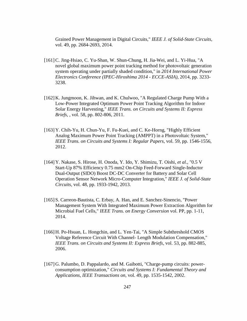
247
Grained Power Management in Digital Circuits," IEEE J. of Solid-State Circuits,
vol. 49, pp. 2684-2693, 2014.
[161] C. Jing-Hsiao, C. Yu-Shan, W. Shun-Chung, H. Jia-Wei, and L. Yi-Hua, "A
novel global maximum power point tracking method for photovoltaic generation
system operating under partially shaded condition," in 2014 International Power
Electronics Conference (IPEC-Hiroshima 2014 - ECCE-ASIA), 2014, pp. 3233-
3238.
[162] K. Jungmoon, K. Jihwan, and K. Chulwoo, "A Regulated Charge Pump With a
Low-Power Integrated Optimum Power Point Tracking Algorithm for Indoor
Solar Energy Harvesting," IEEE Trans. on Circuits and Systems II: Express
Briefs, , vol. 58, pp. 802-806, 2011.
[163] Y. Chih-Yu, H. Chun-Yu, F. Fu-Kuei, and C. Ke-Horng, "Highly Efficient
Analog Maximum Power Point Tracking (AMPPT) in a Photovoltaic System,"
IEEE Trans. on Circuits and Systems I: Regular Papers, vol. 59, pp. 1546-1556,
2012.
[164] Y. Nakase, S. Hirose, H. Onoda, Y. Ido, Y. Shimizu, T. Oishi, et al., "0.5 V
Start-Up 87% Efficiency 0.75 mm2 On-Chip Feed-Forward Single-Inductor
Dual-Output (SIDO) Boost DC-DC Converter for Battery and Solar Cell
Operation Sensor Network Micro-Computer Integration," IEEE J. of Solid-State
Circuits, vol. 48, pp. 1933-1942, 2013.
[165] S. Carreon-Bautista, C. Erbay, A. Han, and E. Sanchez-Sinencio, "Power
Management System With Integrated Maximum Power Extraction Algorithm for
Microbial Fuel Cells," IEEE Trans. on Energy Conversion vol. PP, pp. 1-11,
2014.
[166] H. Po-Hsuan, L. Hongchin, and L. Yen-Tai, "A Simple Subthreshold CMOS
Voltage Reference Circuit With Channel- Length Modulation Compensation,"
IEEE Trans. on Circuits and Systems II: Express Briefs, vol. 53, pp. 882-885,
2006.
[167] G. Palumbo, D. Pappalardo, and M. Gaibotti, "Charge-pump circuits: power-
consumption optimization," Circuits and Systems I: Fundamental Theory and
Applications, IEEE Transactions on, vol. 49, pp. 1535-1542, 2002.

248
[168] J. Torres, M. El-Nozahi, A. Amer, S. Gopalraju, R. Abdullah, K. Entesari, et al.,
"Low Drop-Out Voltage Regulators: Capacitor-less Architecture Comparison,"
IEEE Circuits and Systems Magazine, vol. 14, pp. 6-26, 2014.
[169] A. S. Weddell, G. V. Merrett, and B. M. Al-Hashimi, "Photovoltaic Sample-and-
Hold Circuit Enabling MPPT Indoors for Low-Power Systems," IEEE Trans. on
Circuits and Systems I: Regular Papers, vol. 59, pp. 1196-1204, 2012.
[170] Monnit Wireless Temperature Sensor Datasheet 2013. MNS-9-TS-W1-ST
Available:
http://resources.monnit.com/content/documents/datasheets/commercial/MD001-
Temperature-Sensor-Data-Sheet.pdf
[171] P. Huan, T. Nghia, Y. Youngoo, and H. Deukhyoun, "CMOS Startup Charge
Pump With Body Bias and Backward Control for Energy Harvesting Step-Up
Converters," IEEE Trans. on Circuits and Systems I: Regular Papers vol. 61, pp.
1618-1628, 2014.

249
APPENDIX
Fig. 143. 9 stage I-DCDC converter with associated capacitor voltages.
Small-signal control-to-input transfer function
The following appendix will demonstrate how the small-signal used in the MPPT
control loop was obtained.
The transfer function is obtained by solving for the time domain transient
response in both charging and discharging phases (Fig. 143). Once the time domain
behavior equations are acquired, an averaged value solution follows:
𝐶𝑀𝐹𝐶 ∙
𝑑Vin
𝑑𝑡= (𝐴𝑀𝐹𝐶𝛷1) (Ton (Fsw))
+ (𝐴𝑀𝐹𝐶𝛷2)(Toff(Fsw))
(104)
𝐶𝑖 ∙
𝑑Vi
𝑑𝑡= (𝐴𝐶𝑖𝜙1) + 𝐴𝐶𝑖+1𝜙1)(Ton (Fsw))
+ (𝐴𝐶𝑖𝜙2 + 𝐴𝐶𝑖+1𝜙2)(Toff(Fsw))
(105)
Φ1
Φ2 Φ1
C1
Vin
VMFC
RMFC
CMFC
Φ2
Φ2 Φ1
C9
Vin
Cout Iload
V1 V9 VoutΦ1 Φ2

250
where AMFCΦ1, AMFCΦ2, (ACiϕ1) + (ACi+1ϕ1), and (ACiϕ2) + (ACi+1ϕ2) are the
associated time capacitor charging currents referred to each particular stage capacitor,
the term Ton and Toff is the on and off time for each phase (50% of the period for charge-
discharge phases), and Fsw is the steady stage value of the switching frequency.
𝐶𝑀𝐹𝐶 ∙
𝑑(Vin + 𝑣𝑖𝑛)
𝑑𝑡
= (𝐴𝑀𝐹𝐶𝛷1 + 𝑎𝑀𝐹𝐶𝛷1) (Ton (Fsw + 𝑓𝑠𝑤))
+ (𝐴𝑀𝐹𝐶𝛷2 + 𝑎𝑀𝐹𝐶𝛷2)(Toff(Fsw + 𝑓𝑠𝑤))
(106)
𝐶𝑖 ∙
𝑑(Vi + 𝑣𝑖)
𝑑𝑡= ((𝐴𝐶𝑖𝜙1 + 𝑎𝐶𝑖𝜙1) + (𝐴𝐶𝑖+1𝜙1
+ 𝑎𝐶𝑖+1𝜙1))(Ton (Fsw + 𝑓𝑠𝑤))
+ ((𝐴𝐶𝑖𝜙2 + 𝑎𝐶𝑖𝜙2) + (𝐴𝐶𝑖+1𝜙2
+ 𝑎𝐶𝑖+1𝜙2))(Toff(Fsw + 𝑓𝑠𝑤))
(107)
As shown in Chapter II, a small signal perturbation is introduced to obtain the
control to input transfer function. Once second order terms (non-linear) and DC terms
(no perturbation) are discarded, the linearized (steady-state) transfer function is obtained.
where 𝑎𝑀𝐹𝐶𝛷1, 𝑎𝑀𝐹𝐶𝛷2, 𝑎𝐶𝑖𝜙1 + 𝑎𝐶𝑖+1𝜙1, and 𝑎𝐶𝑖𝜙2 + 𝑎𝐶𝑖+1𝜙2 are the small signal
perturbation induced to each particular stage capacitor and 𝑓𝑠𝑤 the small signal
perturbation of the switching frequency. For the following design the postulation is made
that the output node (𝑉𝑜𝑢𝑡) is under light load with a large valued output capacitor (100
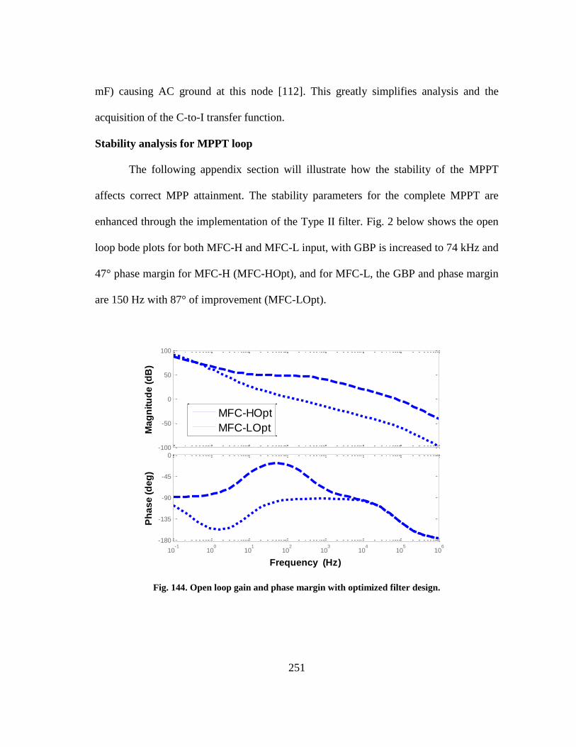
251
mF) causing AC ground at this node [112]. This greatly simplifies analysis and the
acquisition of the C-to-I transfer function.
Stability analysis for MPPT loop
The following appendix section will illustrate how the stability of the MPPT
affects correct MPP attainment. The stability parameters for the complete MPPT are
enhanced through the implementation of the Type II filter. Fig. 2 below shows the open
loop bode plots for both MFC-H and MFC-L input, with GBP is increased to 74 kHz and
47° phase margin for MFC-H (MFC-HOpt), and for MFC-L, the GBP and phase margin
are 150 Hz with 87° of improvement (MFC-LOpt).
Fig. 144. Open loop gain and phase margin with optimized filter design.
-100
-50
0
50
100
Ma
gn
itu
de
(d
B)
10-1
100
101
102
103
104
105
106
-180
-135
-90
-45
0
Ph
as
e (
de
g)
Frequency (Hz)
MFC-HOpt
MFC-LOpt
252
By not optimizing loop stability parameters in the full MPPT open loop,
whenever a switch between sources occurs, a faulty MPP will occur. The simulation in
Fig. 145 shows this behavior when implementing a 1 nF capacitor as the filter, F(s), for
the MPPT control loop.
Fig. 145. Effect of stability in MPPT when switching between MFCs (MFC-H to MFC-L) and
unstable response.