powerdaq user manual - aalborg...
TRANSCRIPT
i
PowerDAQ User Manual
PD2/PDXI-MF Series Multifunction DAQ Boards
PD2/PDXI-MFS Series Simultaneous Sampling DAQ Boards
PDL-MF “Lab” Series Multifunction DAQ Boards
April 2006 Edition PN: PDAQ-MAN-MFX Rev. 6.0.1
© Copyright 1998-2006 United Electronic Industries, Inc. All rights reserved

ii
No part of this publication may be reproduced, stored in a retrieval system, or transmitted, in any
form by any means, electronic, mechanical, by photocopying, recording, or otherwise without
prior written permission.
March 2006 Printing
Information furnished in this manual is believed to be accurate and reliable. However, no
responsibility is assumed for its use, or for any infringements of patents or other rights of third
parties that may result from its use.
All product names listed are trademarks or trade names of their respective companies.
Contacting United Electronic Industries
Mailing Address:
611 Neponset St
Canton, MA 02021
U.S.A.
Support:
Telephone: (781) 821-2890
Fax: (781) 821-2891
Also see the FAQs and online “Live Help” feature on our web site.
Internet Access:
Support [email protected]
Web site www.ueidaq.com
FTP site ftp://ftp.ueidaq.com

iii
Table of Contents
1. Introduction ....................................................................................................... 1 Who should read this manual?...................................................................................................... 1 Conventions.................................................................................................................................. 2 Organization of this manual ......................................................................................................... 3
2. PowerDAQ MF/MFS Series Features Overview............................................ 7 Overview ...................................................................................................................................... 7 Features ........................................................................................................................................ 7 PowerDAQ Models ...................................................................................................................... 8
3. Installation and Configuration....................................................................... 15 Before you begin ........................................................................................................................ 15 Installing the software ................................................................................................................ 16 Installing PowerDAQ hardware ................................................................................................. 17 Confirming the installation......................................................................................................... 18 Configuring a PowerDAQ board................................................................................................ 19 Connector for PDL-MF .............................................................................................................. 31 Connectors for PDXI MF(S) Series boards ................................................................................ 33 “Simple Test” program............................................................................................................... 35 Calibration .................................................................................................................................. 36
4. PowerDAQ Architecture ............................................................................... 37 Functional Overview .................................................................................................................. 37 Programming Model................................................................................................................... 42
5. Analog-Input Subsystem................................................................................ 45 Architecture ................................................................................................................................ 45 Input Ranges............................................................................................................................... 45 Gain Settings .............................................................................................................................. 46 Channel List ............................................................................................................................... 46 Input modes ................................................................................................................................ 47 Sequential vs simultaneous sampling ......................................................................................... 52 Clocking and Triggering............................................................................................................. 56 Clocking/Triggering Examples................................................................................................... 61 The A/D Sample FIFO ............................................................................................................... 64 Moving data into the host PC ..................................................................................................... 64 Host-based buffer usage ............................................................................................................. 69 Data format................................................................................................................................. 70 Programming Techniques........................................................................................................... 73 Method A—Single scan ............................................................................................................. 73 Method B—Burst buffered acquisition (1-shot) ......................................................................... 75 Method C—Continuous acquisition using the Advanced Circular Buffer (ACB)...................... 79

Table of Contents
iv
Method D—Recycled-buffer mode.............................................................................................81 Combining Analog and Digital subsystems ................................................................................82 Synchronous stimulus/response ..................................................................................................82
6. Analog-Output Subsystem..............................................................................84 Architecture.................................................................................................................................84 Single-value update method........................................................................................................84 Buffered waveform generation methods .....................................................................................84 Non-buffered waveform generation methods..............................................................................85 Channel List ................................................................................................................................86 Clocking......................................................................................................................................86 Triggering ...................................................................................................................................87 Programming Techniques ...........................................................................................................87 Method A—Single update...........................................................................................................87 Method B—Single-shot waveform generation............................................................................88 Method C—Continuous waveform generation ...........................................................................89 Method D—Repetitive waveform generation .............................................................................91 Method E—Autoregeneration .....................................................................................................92 Method F—Event-based waveforms using PCI interrupts..........................................................93
7. Digital I/O Subsystem......................................................................................96 Architecture.................................................................................................................................96 Programming Techniques ...........................................................................................................97 Method A—Polled I/O................................................................................................................97 Method B—Generate an event upon edge detection...................................................................99
8. User Counter/Timer Subsystem...................................................................102 Architecture...............................................................................................................................102 PDL-MF....................................................................................................................................104 Programming Techniques .........................................................................................................105
9. Support Software...........................................................................................108 PowerDAQ Example Programs ................................................................................................108 Third-Party Software Support ...................................................................................................110
Appendix A: Specifications...............................................................................112 PD2-MF Multifunction Boards .................................................................................................113 PD2-MFS Simultaneous Sampling Boards ...............................................................................117 PDL-MF “Lab” Multifunction Board .......................................................................................121 PDXI-MF Multifunction Boards...............................................................................................123 PDXI-MFS Simultaneous Sampling Boards.............................................................................127
Appendix B: PowerDAQ A/D Timing .............................................................132 PD2-MF Series Timing .............................................................................................................133 PD2-MFS Series Timing...........................................................................................................133 PDL-MF Series Timing.............................................................................................................133 PDXI-MF Series Timing...........................................................................................................134 PDXI-MFS Series Timing.........................................................................................................134
Table of Contents
v
Appendix C: Accessories .................................................................................. 136 Screw-Terminal Panels (PD2/PDXI)........................................................................................ 136 Screw Terminal Panels (PDL-MF only)................................................................................... 136 BNC & Distribution Panels (PD2/PDXI) ................................................................................. 137 Cables (PD2/PDXI) ................................................................................................................. 137 Mating cables, connectors, rack mounts (PD2/PDXI).............................................................. 138 Signal Conditioning (all boards)............................................................................................... 139
Appendix D: PowerDAQ SDK Structure........................................................ 140 PowerDAQ Windows device drivers........................................................................................ 141 PowerDAQ Windows DLLs..................................................................................................... 141 PowerDAQ Language Libraries ............................................................................................... 142 PowerDAQ Include Files.......................................................................................................... 143 PowerDAQ Linux support........................................................................................................ 145 PowerDAQ QNX Support ........................................................................................................ 145
Appendix E: Application Notes........................................................................ 146 1. PowerDAQ Advanced Circular Buffer (ACB) ..................................................................... 146 2. PD-BNC-xx wiring options: ................................................................................................. 149
Appendix F: Warranty ..................................................................................... 150
Appendix G: Glossary....................................................................................... 151
Index ................................................................................................................... 163
Reader Feedback ............................................................................................... 168

vi
List of Tables and Figures
Table 2.1—PowerDAQ PD2-MF Series models ..............................................................................9 Table 2.2—PowerDAQ PD2-MFS Models ....................................................................................10 Table 2.3—PowerDAQ PDXI-MF Series Models..........................................................................11 Table 2.4—PowerDAQ PDXI-MFS Models ..................................................................................12 Table 2.5—MFS Differential Upgrade Options..............................................................................13 Table 2.6—PD2-/PDXI FIFO upgrade option ................................................................................13 Table 2.7—PDL-MF board specifications ......................................................................................14 Figure 3.1—PowerDAQ Software Installation Startup Screen .......................................................16 Figure 3.2—Control Panel Application ..........................................................................................18 Figure 3.3a—Connector layout for long-slot PD2 Family boards ..................................................19 Figure 3.3b—Connector layout for “sandwich” format PD2 family boards ...................................20 Figure 3.4—Connector layout for PDXI-MF(S) Series boards.......................................................21 Figure 3.5—Connector layout for PDL-MF board. ........................................................................22 Figure 3.6—PDXI Configurator .....................................................................................................23 Figure 3.7—Cable connection diagram for PowerDAQ MF (S) boards.........................................25 Figure 3.8a—Physical layout of J1 / JA1 Connector on PD2 MF(S) Series boards .......................25 Figure 3.8b—Pin assignments on J1 / JA1 Connector on PD2-MF boards,
in single-ended mode ....................................................................................................26 Figure 3.8c—Pin assignments on J1 / JA1 Connector on PD2-MF boards,
in differential mode .......................................................................................................27 Figure 3.8d—J1 / JA1 Connector on PD2-MFS boards, single-ended or
differential modes..........................................................................................................28 Figure 3.9a—Physical layout of J2 on PD2 MF/MFS Series boards .............................................29 Figure 3.9b—Pin assignments for J2 Connector on PD2-MF/MFS boards ....................................29 Figure 3.10a—Physical layout of J4 on PD2 MF/MFS Series boards ............................................30 Figure 3.10b—Pin assignments for J4 Connector on PD2-MF/MFS boards ..................................30 Figure 3.11a—Physical layout of J6 on PD2-MF(S) Series boards ................................................31 Figure 3.11b—Pin assignments for J6 Connector on PD2-MF/MFS boards ..................................31 Figure 3.12a—Physical layout of J1 on PDL-MF board................................................................31 Figure 3.12b—Pin assignments for J1 Connector on PDL-MF Series board..................................32 Figure 3.13—Cable connection diagram for PDXI-MF(S) boards .................................................33 Figure 3.14a—Physical layout of J2 on PDXI-MF/MFS Series boards.........................................33 Figure 3.14b—Pin assignments of J2 Connector on PDXI MF/MFS Series boards.......................34 Figure 3.15—Simple Test application ............................................................................................35 Figure 4.1—PowerDAQ PD2-MF/MFS Series block diagram.......................................................37 Figure 4.2—PowerDAQ PDXI-MF/MFS Series block diagram.....................................................38 Figure 4.3—PowerDAQ PDL-MF block diagram..........................................................................39 Figure 4.4—Communication between a user application and a PowerDAQ
multifunction board........................................................................................................42 Table 5.1—PowerDAQ analog-input ranges ..................................................................................45 Table 5.2—Programmable Gains....................................................................................................46 Table 5.3a—Channel List format....................................................................................................47 Table 5.3b—Programmable-gain codes..........................................................................................47

List of Tables and Figures
vii
Figure 5.1—Wiring for single-ended and pseudodifferential inputs .............................................. 49 Figure 5.2—Wiring for differential inputs ..................................................................................... 50 Figure 5.3a—Analog front end of a PowerDAQ MF Series board ................................................ 53 Figure 5.3b—Acquisition sequence for multiplexed inputs on
MF Series and PDL boards........................................................................................... 53 Figure 5.4a—Analog front end on PowerDAQ MFS simultaneous-sampling
boards (with both SE and DI modes available) ............................................................ 55 Figure 5.4b—Acquisition sequence for simultaneous inputs using
S/H amplifiers on MFS Series boards........................................................................... 56 Table 5.4—External trigger modes ................................................................................................ 60 Table 5.5—Possible clocking combinations (the shaded rows at the
bottom indicate rarely used combinations). .................................................................... 63 Table 5.6—Default Bus Mastering parameters for various FIFO sizes.......................................... 67 Figure 5.5—Control Panel applet with typical PowerDAQ board settings .................................... 68 Figure 5.6—Advanced Circular Buffer .......................................................................................... 69 Figure 5.7a—PowerDAQ 16-bit data format ................................................................................. 71 Figure 5.7b—PowerDAQ 14-bit data format ................................................................................. 71 Figure 5.7c—PowerDAQ 12-bit data format ................................................................................. 71 Table 5.8—Bit weight by input range ............................................................................................ 71 Table 5.9—Displacement by input range ....................................................................................... 72 Table 5.10—Mode constants for use in analog-input configuration word ..................................... 73 Figure 6-1—Analog-output data format ......................................................................................... 86 Figure 7.1—Digital-input subsystem hardware block diagram...................................................... 96 Figure 7.2—Digital-input configuration word ............................................................................... 97 Table 9.1—Third-party software support ..................................................................................... 110 Figure D.1—PowerDAQ Software Structure ............................................................................... 140 Figure E.1—Advanced Circular Buffer........................................................................................ 147

viii
1
1. Introduction This manual describes the features and functions of hardware in the PowerDAQ series of PCI and
PXI multifunction data-acquisition boards. These high-performance systems support functions
including analog input (AI), analog output (AO), digital I/O (DIO), and user counter/timer I/O
(UCT) for either PCI-bus or PXI/CompactPCI-based systems.
Note All PDXI cards support the PXI Trigger Bus, Star Trigger lines and Local Bus on the P2 connector.
Nonetheless, they run without modification in any C-sized CompactPCI backplane except they lose
support for PXI-specific functions.
These boards all fall into one of the following broad classifications:
• PD2/PDXI-MF Series—Multifunction (analog I/O, digital I/O, counter/timer)
• PD2/PDXI MFS Series—Simultaneous Sampling Multifunction
• PDL-MF—“Lab” Series Entry-level Multifunction
This manual uses the word “PowerDAQ” to collectively reference all the models listed above.
Other boards in the PowerDAQ Series (see separate manuals) include the
• PD2/PDXI-AO Series—Analog Output (with digital I/O, counter/timers)
• PD2/PDXI-DIO Series—Digital I/O (with counter/timers)
• PDL-DIO Series—“Lab” Series Entry-level Digital I/O (with counter/timers)
Who should read this manual?
This manual has been written to make the installation, configuration and operation of our
PowerDAQ multifunction boards as straightforward as possible. However, it assumes that the user
has basic PC skills and is familiar with the Microsoft Windows XP/2000/NT/9x, QNX or
Linux/RTLinux/RTAI Linux operating environments.

1. Introduction
2
Conventions
To help you get the most out of this manual and our products, please note that we use the
following conventions:
Tips are designed to highlight quick ways to get the job done, or reveal good ideas you
might not discover on your own.
Note Notes alert you to important information.
CAUTION! Caution advises you of precautions to take to avoid injury, data loss, or
system crash.
Text formatted in bold typeface generally represents type that should be entered verbatim. For
instance, it can represent a command, as in the following example: “You can instruct users how to
run setup using a command such as setup.exe.”
TIP

1. Introduction
3
Organization of this manual
Chapter 1: Introduction
The section you are reading now. It explains which products are covered and gives you tips on
how to best use this manual.
Chapter 2: PowerDAQ MF/MFS Series Features Overview
This chapter provides an overview of the key features of the PowerDAQ series and detailed
information on the various PowerDAQ models currently available. It also lists what you need to
get started.
Chapter 3: Installation and Configuration
This chapter explains how to install and configure your PowerDAQ board. Among other things, it
shows where various I/O connectors are located on various boards and also shows their pinout
definitions.
Chapter 4: PowerDAQ Architecture
This chapter discusses the subsystems of your PowerDAQ board, and it gives an overview of the
programming model, showing how various cards and software modules intercommunicate.
Chapter 5: Analog-Input Subsystem
This and the following three chapters are each devoted to one of the PowerDAQ MF/MFS Series
subsystems. Each chapter is divided into two major sections. The first gives a description of the
hardware and gives tips for making best use of these features in a test system. The second section
introduces you to the best way to program this subsystem and reviews the most frequently used
commands and operating methods.
Chapter 6: Analog-Output Subsystem
This chapter contains two major sections: the first describes the hardware and its features; the
second introduces you into techniques for programming this subsystem.
Chapter 7: Digital I/O Subsystem
This chapter contains two major sections: the first describes the hardware and its features; the
second introduces you into techniques for programming this subsystem.
Chapter 8: User Counter/Timer Subsystem
This chapter contains two major sections: the first describes the hardware and its features; the
second introduces you into techniques for programming this subsystem.
Chapter 9: Support Software
1. Introduction
4
This chapter outlines the various example programs supplied with the PowerDAQ Software Suite
CD-ROM. It also describes the third-party software we support with PowerDAQ hardware.
Appendix A: Specifications
This appendix lists the hardware specifications of the PowerDAQ product series.
Appendix B: PowerDAQ A/D Timing
This appendix gives tables that help you determine the fastest acquisition times when using
various options such as Slow Bits.
Appendix C: Accessories
This appendix provides a list of available PowerDAQ accessories.
Appendix D: PowerDAQ SDK Structure
This appendix shows the directories and files that are created when you install the PowerDAQ
Software Developers Kit.
Appendix E: Application Notes
This appendix provides application notes to enhance your understanding of PowerDAQ products.
Appendix F: Warranty
This appendix contains a detailed explanation of PowerDAQ warranty.
Appendix G: Glossary
This is an alphabetical listing of the terms used in this manual along with their definitions.
Index
This is an alphabetical listing of the topics covered in this manual.

1. Introduction
5
Other PowerDAQ Documentation
The PowerDAQ PD2 / PDXI / PDL-MF Manual is one part of the documentation available for the
PowerDAQ system. There are several other manuals you might want to read before programming
your application. They are available either on the PowerDAQ Software Suite CD or can be
downloaded from the UEI web site.
Software: PowerDAQ Programmer Manual
PowerDAQ for LabVIEW User Manual
Hardware: PowerDAQ ASTP User Manual
PowerDAQ Thermocouple Rack User Manual.
Feedback
We are interested in any feedback you might have concerning our products and manuals. A Reader
Evaluation form is available on the last page of the manual.

1. Introduction
6
7
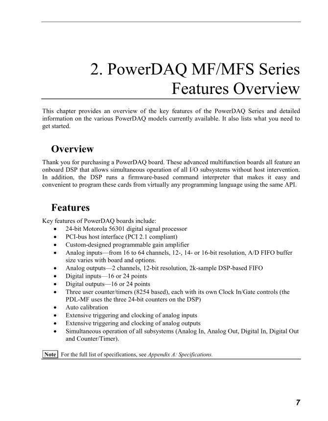
2. PowerDAQ MF/MFS Series
Features Overview This chapter provides an overview of the key features of the PowerDAQ Series and detailed
information on the various PowerDAQ models currently available. It also lists what you need to
get started.
Overview
Thank you for purchasing a PowerDAQ board. These advanced multifunction boards all feature an
onboard DSP that allows simultaneous operation of all I/O subsystems without host intervention.
In addition, the DSP runs a firmware-based command interpreter that makes it easy and
convenient to program these cards from virtually any programming language using the same API.
Features
Key features of PowerDAQ boards include:
• 24-bit Motorola 56301 digital signal processor
• PCI-bus host interface (PCI 2.1 compliant)
• Custom-designed programmable gain amplifier
• Analog inputs—from 16 to 64 channels, 12-, 14- or 16-bit resolution, A/D FIFO buffer
size varies with board and options.
• Analog outputs—2 channels, 12-bit resolution, 2k-sample DSP-based FIFO
• Digital inputs—16 or 24 points
• Digital outputs—16 or 24 points
• Three user counter/timers (8254 based), each with its own Clock In/Gate controls (the
PDL-MF uses the three 24-bit counters on the DSP)
• Auto calibration
• Extensive triggering and clocking of analog inputs
• Extensive triggering and clocking of analog outputs
• Simultaneous operation of all subsystems (Analog In, Analog Out, Digital In, Digital Out
and Counter/Timer).
Note For the full list of specifications, see Appendix A: Specifications.
2. PowerDAQ MF/MFS Series Features Overview
8
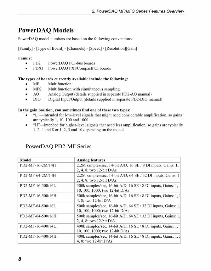
PowerDAQ Models
PowerDAQ model numbers are based on the following conventions:
[Family] - [Type of Board] - [Channels] - [Speed] / [Resolution][Gain]
Family:
• PD2 PowerDAQ PCI-bus boards
• PDXI PowerDAQ PXI/CompactPCI boards
The types of boards currently available include the following:
• MF Multifunction
• MFS Multifunction with simultaneous sampling
• AO Analog Output (details supplied in separate PD2-AO manual)
• DIO Digital Input/Output (details supplied in separate PD2-DIO manual)
In the gain position, you sometimes find one of these two types:
• “L”—intended for low-level signals that might need considerable amplification, so gains
are typically 1, 10, 100 and 1000
• “H”—intended for higher-level signals that need less amplification, so gains are typically
1, 2, 4 and 8 or 1, 2, 5 and 10 depending on the model.
PowerDAQ PD2-MF Series
Model Analog features
PD2-MF-16-2M/14H 2.2M samples/sec, 14-bit A/D, 16 SE / 8 DI inputs, Gains: 1,
2, 4, 8; two 12-bit D/As
PD2-MF-64-2M/14H 2.2M samples/sec, 14-bit A/D, 64 SE / 32 DI inputs, Gains: 1,
2, 4, 8; two 12-bit D/As
PD2-MF-16-500/16L 500k samples/sec, 16-bit A/D, 16 SE / 8 DI inputs, Gains: 1,
10, 100, 1000; two 12-bit D/As
PD2-MF-16-500/16H 500k samples/sec, 16-bit A/D, 16 SE / 8 DI inputs, Gains: 1, 2,
4, 8; two 12-bit D/A
PD2-MF-64-500/16L 500k samples/sec, 16-bit A/D, 64 SE / 32 DI inputs, Gains: 1,
10, 100, 1000; two 12-bit D/As
PD2-MF-64-500/16H 500k samples/sec, 16-bit A/D, 64 SE / 32 DI inputs, Gains: 1,
2, 4, 8; two 12-bit D/A
PD2-MF-16-400/14L 400k samples/sec, 14-bit A/D, 16 SE / 8 DI inputs, Gains: 1,
10, 100, 1000; two 12-bit D/As
PD2-MF-16-400/14H 400k samples/sec, 14-bit A/D, 16 SE / 8 DI inputs, Gains: 1, 2,
4, 8; two 12-bit D/As

2. PowerDAQ MF/MFS Series Features Overview
9
PD2-MF-64-400/14L 400k samples/sec, 14-bit A/D, 64 SE / 32 DI inputs, Gains:
1,10,100,1000; two 12-bit D/As
PD2-MF-64-400/14H 400k samples/sec, 14-bit A/D, 64 SE / 32 DI inputs, Gains: 1,
2, 4, 8; two 12-bit D/A
PD2-MF-16-333/16L 333k samples/sec, 16-bit A/D, 16 SE / 8 DI inputs, Gains: 1,
10, 100, 1000; two 12-bit D/As
PD2-MF-16-333/16H 333k samples/sec, 16-bit A/D, 16 SE / 8 DI inputs, Gains: 1, 2,
4, 8; two 12-bit D/A
PD2-MF-64-333/16L 333k samples/sec, 16-bit A/D, 64 SE / 32 DI inputs, Gains: 1,
10, 100, 1000; two 12-bit D/As
PD2-MF-64-333/16H 333k samples/sec, 16-bit A/D, 64 SE / 32 DI inputs, Gains: 1,
2, 4, 8; two 12-bit D/A
PD2-MF-16-150/16L 150k samples/sec, 16-bit A/D, 16 SE / 8 DI inputs, Gains: 1,
10, 100, 1000; two 12-bit D/As
PD2-MF-16-150/16H 150k samples/sec, 16-bit A/D, 16 SE / 8 DI inputs, Gains: 1, 2,
4, 8; two 12-bit D/A
Table 2.1—PowerDAQ PD2-MF Series models
Note All PD2-MF Series models also include three counter/timers and 32 digital I/O lines.
2. PowerDAQ MF/MFS Series Features Overview
10
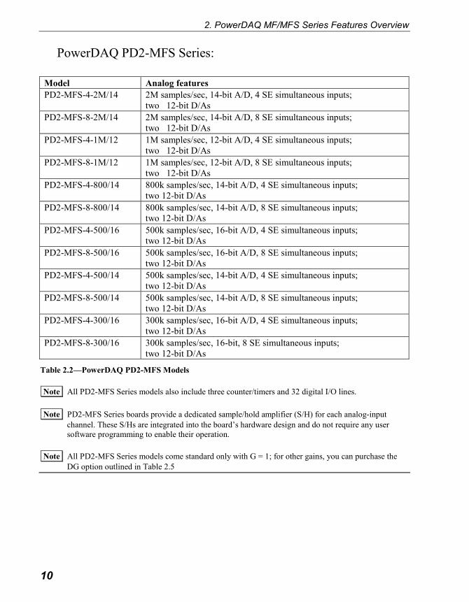
PowerDAQ PD2-MFS Series:
Model Analog features
PD2-MFS-4-2M/14 2M samples/sec, 14-bit A/D, 4 SE simultaneous inputs;
two 12-bit D/As
PD2-MFS-8-2M/14 2M samples/sec, 14-bit A/D, 8 SE simultaneous inputs;
two 12-bit D/As
PD2-MFS-4-1M/12 1M samples/sec, 12-bit A/D, 4 SE simultaneous inputs;
two 12-bit D/As
PD2-MFS-8-1M/12 1M samples/sec, 12-bit A/D, 8 SE simultaneous inputs;
two 12-bit D/As
PD2-MFS-4-800/14 800k samples/sec, 14-bit A/D, 4 SE simultaneous inputs;
two 12-bit D/As
PD2-MFS-8-800/14 800k samples/sec, 14-bit A/D, 8 SE simultaneous inputs;
two 12-bit D/As
PD2-MFS-4-500/16 500k samples/sec, 16-bit A/D, 4 SE simultaneous inputs;
two 12-bit D/As
PD2-MFS-8-500/16 500k samples/sec, 16-bit A/D, 8 SE simultaneous inputs;
two 12-bit D/As
PD2-MFS-4-500/14 500k samples/sec, 14-bit A/D, 4 SE simultaneous inputs;
two 12-bit D/As
PD2-MFS-8-500/14 500k samples/sec, 14-bit A/D, 8 SE simultaneous inputs;
two 12-bit D/As
PD2-MFS-4-300/16 300k samples/sec, 16-bit A/D, 4 SE simultaneous inputs;
two 12-bit D/As
PD2-MFS-8-300/16 300k samples/sec, 16-bit, 8 SE simultaneous inputs;
two 12-bit D/As
Table 2.2—PowerDAQ PD2-MFS Models
Note All PD2-MFS Series models also include three counter/timers and 32 digital I/O lines.
Note PD2-MFS Series boards provide a dedicated sample/hold amplifier (S/H) for each analog-input
channel. These S/Hs are integrated into the board’s hardware design and do not require any user
software programming to enable their operation.
Note All PD2-MFS Series models come standard only with G = 1; for other gains, you can purchase the
DG option outlined in Table 2.5

2. PowerDAQ MF/MFS Series Features Overview
11
PowerDAQ PDXI-MF Series
Model Analog features
PDXI-MF-16-2M/14H 2.2M samples/sec, 14-bit A/D, 16 SE / 8 DI inputs,
Gains: 1, 2, 4, 8; two 12-bit D/As
PDXI-MF-64-2M/14H 2.2M samples/sec, 14-bit A/D, 64 SE / 32 DI inputs,
Gains: 1, 2, 4, 8; two 12-bit D/As
PDXI-MF-16-1M/12L 1.25M samples/sec, 12-bit A/D, 16 SE / 8 DI inputs,
Gains: 1, 10, 100, 1000; two 12-bit D/As
PDXI-MF-16-1M/12H 1.25M samples/sec, 12-bit A/D, 16 SE / 8 DI inputs,
Gains: 1, 2, 4, 8; two 12-bit D/A
PDXI-MF-64-1M/12L 1.25M samples/sec, 12-bit A/D, 64 SE / 32 DI inputs, Gains: 1, 10,
100, 1000; two 12-bit D/As
PDXI-MF-64-1M/12H 1.25M samples/sec, 12-bit A/D, 64 SE / 32 DI inputs, Gains: 1, 2,
4, 8; two 12-bit D/As
PDXI-MF-16-500/16L 500k samples/sec, 16-bit A/D, 16 SE / 8 DI inputs,
Gains: 1, 10, 100, 1000; two 12-bit D/As
PDXI-MF-16-500/16H 500k samples/sec, 16-bit A/D, 16 SE / 8 DI inputs,
Gains: 1, 2, 4, 8; two 12-bit D/As
PDXI-MF-64-500/16L 500k samples/sec, 16-bit A/D, 64 SE / 32 DI inputs,
Gains: 1, 10, 100, 1000; two 12-bit D/As
PDXI-MF-64-500/16H 500k samples/sec, 16-bit A/D, 64 SE / 32 DI inputs,
Gains: 1, 2, 4, 8; two 12-bit D/As
PDXI-MF-16-400/14L 400k samples/sec, 14-bit A/D, 16 SE / 8 DI inputs,
Gains: 1, 10, 100, 1000; two 12-bit D/As
PDXI-MF-16-400/14H 400k samples/sec, 14-bit A/D, 16 SE / 8DI inputs,
Gains: 1, 2, 4, 8; two 12-bit D/As
PDXI-MF-64-400/14L 400k samples/sec, 14-bit A/D, 64 SE / 32 DI inputs,
Gains: 1, 10, 100, 1000; two 12-bit D/As
PDXI-MF-64-400/14H 400k samples/sec, 14-bit A/D, 64 SE / 32 DI inputs,
Gains: 1, 2, 4, 8; two 12-bit D/As
PDXI-MF-16-333/16L 333k samples/sec, 16-bit A/D, 16 SE / 8 DI inputs,
Gains: 1, 10, 100, 1000; two 12-bit D/As
PDXI-MF-16-333/16H 333k samples/sec, 16-bit A/D, 16 SE / 8 DI inputs,
Gains: 1, 2, 4, 8; two 12-bit D/As
PDXI-MF-64-333/16L 333k samples/sec, 16-bit A/D, 64 SE / 32 DI inputs,
Gains: 1, 10, 100, 1000; two 12-bit D/As
PDXI-MF-64-333/16H 333k samples/sec, 16-bit A/D, 64 SE / 32 DI inputs,
Gains: 1, 2, 4, 8; two 12-bit D/A
PDXI-MF-16-150/16L 150k samples/sec, 16-bit A/D, 16 SE / 8 DI inputs,
Gains: 1, 10, 100, 1000; two 12-bit D/As
PDXI-MF-16-150/16H 150k samples/sec, 16-bit A/D, 16 SE / 8 DI inputs,
Gains: 1, 2, 4, 8; two 12-bit D/As
Table 2.3—PowerDAQ PDXI-MF Series Models
Note All PDXI-MF Series models also include three counter/timers and 32 digital I/O lines.

2. PowerDAQ MF/MFS Series Features Overview
12
PowerDAQ PDXI-MFS Series
Model Analog features
PDXI-MFS-4-2M/14 2M samples/sec, 14-bit A/D, 4 SE simultaneous
inputs, G = 1; two 12-bit D/As
PDXI-MFS-8-2M/14 2M samples/sec, 14-bit A/D, 8 SE simultaneous
inputs, G = 1; two 12-bit D/As, G = 1
PDXI-MFS-4-1M/12 1M samples/sec, 12-bit A/D, 4 SE simultaneous
inputs, G = 1; two 12-bit D/As
PDXI-MFS-8-1M/12 1M samples/sec, 12-bit A/D, 8 SE simultaneous
inputs, G = 1; two 12-bit D/As
PDXI-MFS-4-800/14 800k samples/sec, 14-bit A/D, 4 SE simultaneous inputs, G =
1; two 12-bit D/As, G = 1
PDXI-MFS-8-800/14 800k samples/sec, 14-bit A/D, 8 SE simultaneous inputs, G =
1; two 12-bit D/As,
PDXI-MFS-4-500/16 500k samples/sec, 16-bit A/D, 4 SE simultaneous inputs, G =
1; two 12-bit D/As
PDXI-MFS-8-500/16 500k samples/sec, 16-bit A/D, 8 SE simultaneous inputs, G =
1; two 12-bit D/As
PDXI-MFS-4-500/14 500k samples/sec, 14-bit A/D, 4 SE simultaneous inputs, G =
1; two 12-bit D/As
PDXI-MFS-8-500/14 500k samples/sec, 14-bit A/D, 8 SE simultaneous inputs, G =
1; two 12-bit D/As
PDXI-MFS-4-300/16 300k samples/sec, 16-bit A/D, 4 SE simultaneous inputs, G =
1; two 12-bit D/As
PDXI-MFS-8-300/16 300k samples/sec, 16-bit A/D, 8 SE simultaneous inputs, G =
1; two 12-bit D/As
Table 2.4—PowerDAQ PDXI-MFS Models
Note All PDXI-MFS Series models also include three counter/timers and 32 digital I/O lines.
Note PDXI-MFS Series boards provide a dedicated sample/hold amplifier (S/H) for each analog-input
channel. These S/Hs are integrated into the board’s hardware design and do not require any user
software programming to enable their operation.
Note All PDXI-MFS Series models come standard only with G = 1; for other gains, you can purchase the
DG option outlined in Table 2.5

2. PowerDAQ MF/MFS Series Features Overview
13
PowerDAQ PD2/PDXI MFS Series differential upgrade
with gains (DG option)
The PD2/PDXI-MFS (simultaneous-sampling) Series can be upgraded from single-ended to
differential inputs with gains for each channel. One programmable-gain amplifier (PGA) per
channel is installed on the board.
Upgrade Part Number Additional features added
PD2-MFS-4-DG4 Upgrade any PD2-MFS board from 4 SE to 4 DI and add Gains =
1, 2, 5, 10
PD2-MFS-8-DG8 Upgrade any PD2-MFS board from 8 SE to 8 DI and add Gains =
1, 2, 5, 10
PDXI-MFS-4-DG4 Upgrade any PDXI-MFS board from 4 SE to 4 DI and add Gains =
1, 2, 5, 10
PDXI-MFS-8-DG8 Upgrade any PDXI-MFS board from 8 SE to 8 DI and add Gain =
1, 2, 5, 10
Table 2.5—MFS Differential Upgrade Options
Note PowerDAQ MFS boards with the -DGx option installed have the same number of single-ended or
differential channels.
PowerDAQ MF/MFS FIFO upgrade options:
You can upgrade the analog-input FIFOs on PD2/PDXI PowerDAQ multifunction boards. Below
is a list of currently available upgrade options:
Upgrade part number Additional features added
PD-16KFIFO Upgrade onboard analog-input FIFO buffer to 16k samples
PD-32KFIFO Upgrade onboard analog-input FIFO buffer to 32k samples
PD-64KFIFO Upgrade onboard analog-input FIFO buffer to 64k samples
Table 2.6—PD2-/PDXI FIFO upgrade option
2. PowerDAQ MF/MFS Series Features Overview
14
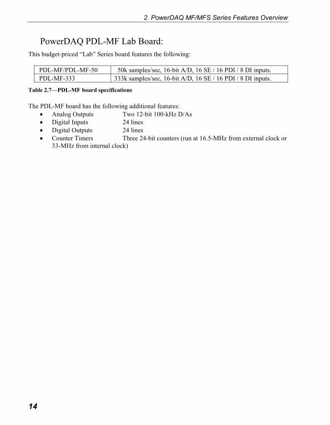
PowerDAQ PDL-MF Lab Board:
This budget-priced “Lab” Series board features the following:
PDL-MF/PDL-MF-50 50k samples/sec, 16-bit A/D, 16 SE / 16 PDI / 8 DI inputs.
PDL-MF-333 333k samples/sec, 16-bit A/D, 16 SE / 16 PDI / 8 DI inputs.
Table 2.7—PDL-MF board specifications
The PDL-MF board has the following additional features:
• Analog Outputs Two 12-bit 100-kHz D/As
• Digital Inputs 24 lines
• Digital Outputs 24 lines
• Counter Timers Three 24-bit counters (run at 16.5-MHz from external clock or
33-MHz from internal clock)

15
3. Installation and Configuration
Before you begin
Before installing your PowerDAQ board, be sure to read and understand the following
information.
System requirements
To install and run a PowerDAQ board, you need the following:
• A PCI-bus system, a PXI-bus system or a CompactPCI-bus system with a free slot, a
Pentium-class processor, and a BIOS compliant with PCI Local Bus Specification Rev 2.1
or greater
• Windows 95, 98, NT 4.0, 2000/XP, Linux, Realtime Linux or QNX
Packing list
In your PowerDAQ package, you should have received the following:
• a PowerDAQ board
• a calibration certificate
• this User Manual
• a CD containing the PowerDAQ Software Suite, including the full Software
Development Kit (SDK) and documentation
Note The CD label shows the version number of the SDK.
Precautions
PowerDAQ boards contain sensitive electronic components. When handling your PowerDAQ
board, you should:
• ensure that you are properly grounded.
• discharge any static electricity by touching the metal part of your PC while holding the
board in its antistatic bag.

3. Installation and Configuration
16
Installing the software
Note All third-party software must be installed prior to installing the PowerDAQ SDK.
Note The PowerDAQ SDK must be installed before you plug in a PowerDAQ board to ensure that the
driver properly detects the board.
To install the PowerDAQ SDK:
1. Start your PC and, if running Windows NT, 2000 or XP, log in as an administrator.
2. Insert the PowerDAQ Software Suite CD into your CD-ROM drive. Windows
should automatically start the PowerDAQ Setup program. If you see the UEI logo
and then the PowerDAQ Welcome screen, go to Step 6.
3. If the Setup program does not start automatically, select Run from the Start menu.
4. Enter D:\Setup.exe in the Open: textbox (substitute the correct letter if D is not the
drive letter for your CD-ROM drive.)
5. Click OK.
Figure 3.1—PowerDAQ Software Installation Startup Screen
6. As the Setup program runs, you will be asked to enter information about your
PowerDAQ configuration. Unless you are an expert user and have specific
3. Installation and Configuration
17
requirements, you should select a Typical installation and accept the default
configuration.
7. If the Setup program asks for information about third-party software packages that
you do not have installed on your PC, leave the text box blank and click the Next
button.
8. When the installation is complete, restart your PC when prompted.
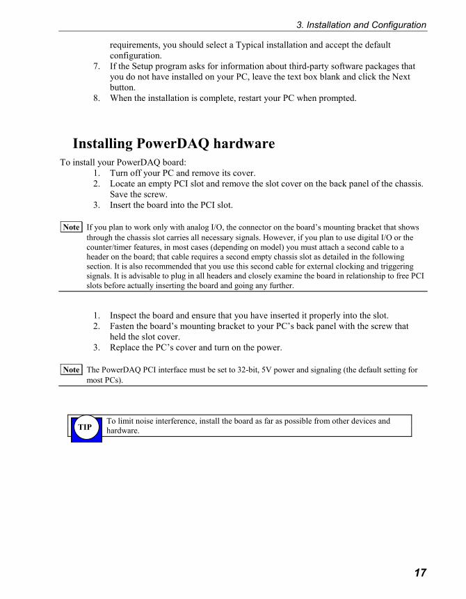
Installing PowerDAQ hardware
To install your PowerDAQ board:
1. Turn off your PC and remove its cover.
2. Locate an empty PCI slot and remove the slot cover on the back panel of the chassis.
Save the screw.
3. Insert the board into the PCI slot.
Note If you plan to work only with analog I/O, the connector on the board’s mounting bracket that shows
through the chassis slot carries all necessary signals. However, if you plan to use digital I/O or the
counter/timer features, in most cases (depending on model) you must attach a second cable to a
header on the board; that cable requires a second empty chassis slot as detailed in the following
section. It is also recommended that you use this second cable for external clocking and triggering
signals. It is advisable to plug in all headers and closely examine the board in relationship to free PCI
slots before actually inserting the board and going any further.
1. Inspect the board and ensure that you have inserted it properly into the slot.
2. Fasten the board’s mounting bracket to your PC’s back panel with the screw that
held the slot cover.
3. Replace the PC’s cover and turn on the power.
Note The PowerDAQ PCI interface must be set to 32-bit, 5V power and signaling (the default setting for
most PCs).
To limit noise interference, install the board as far as possible from other devices and
hardware.
TIP
3. Installation and Configuration
18
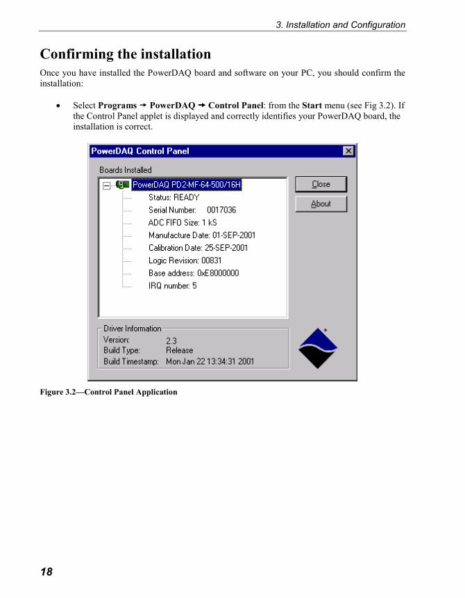
Confirming the installation
Once you have installed the PowerDAQ board and software on your PC, you should confirm the
installation:
• Select Programs PowerDAQ Control Panel: from the Start menu (see Fig 3.2). If
the Control Panel applet is displayed and correctly identifies your PowerDAQ board, the
installation is correct.
Figure 3.2—Control Panel Application
3. Installation and Configuration
19
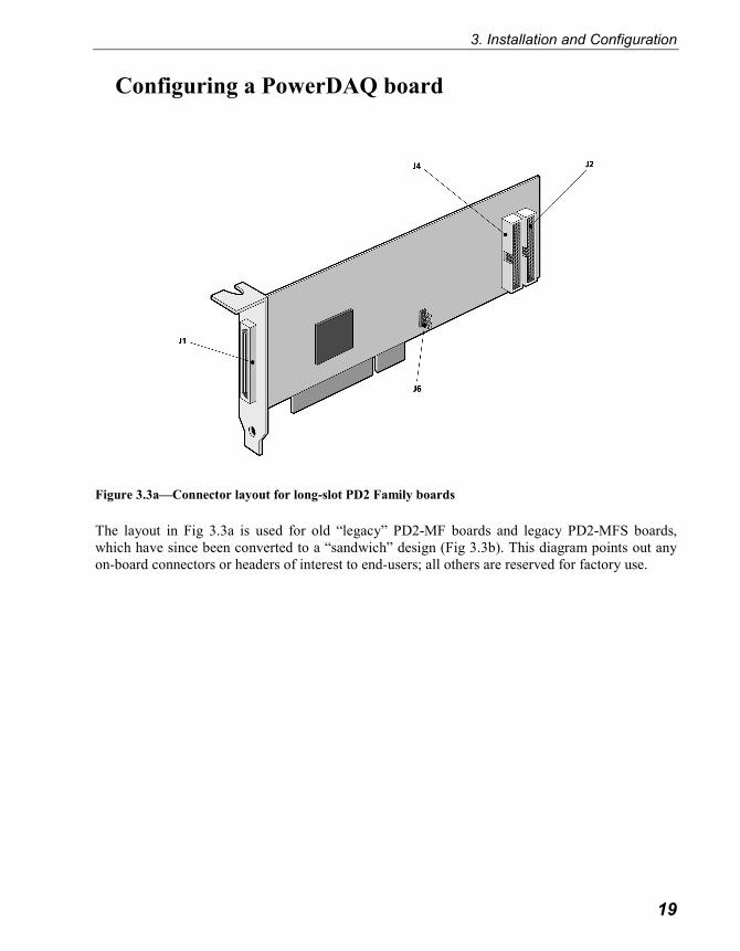
Configuring a PowerDAQ board
Figure 3.3a—Connector layout for long-slot PD2 Family boards
The layout in Fig 3.3a is used for old “legacy” PD2-MF boards and legacy PD2-MFS boards,
which have since been converted to a “sandwich” design (Fig 3.3b). This diagram points out any
on-board connectors or headers of interest to end-users; all others are reserved for factory use.
3. Installation and Configuration
20
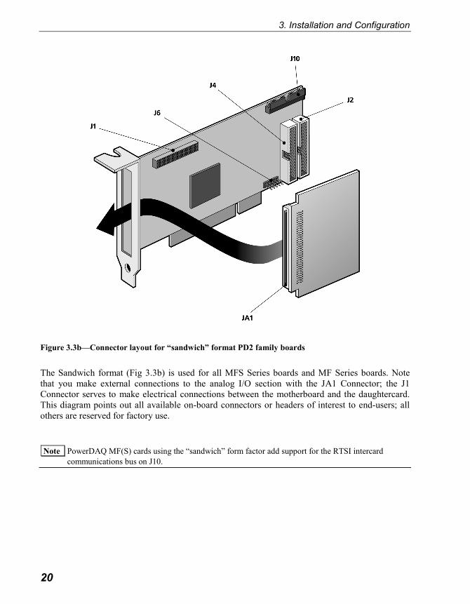
Figure 3.3b—Connector layout for “sandwich” format PD2 family boards
The Sandwich format (Fig 3.3b) is used for all MFS Series boards and MF Series boards. Note
that you make external connections to the analog I/O section with the JA1 Connector; the J1
Connector serves to make electrical connections between the motherboard and the daughtercard.
This diagram points out all available on-board connectors or headers of interest to end-users; all
others are reserved for factory use.
Note PowerDAQ MF(S) cards using the “sandwich” form factor add support for the RTSI intercard
communications bus on J10.

3. Installation and Configuration
21
Note Some PD2 Family boards now ship in the alternate short-slot “sandwich” form factor in Fig 3-3b. At
the time of this writing, they include all PD2-MFS Series boards as well as the PD2-MF-xx-2M
Series boards. We anticipate that other boards will use this form factor in the future. The location of
the headers might change from the previous long-card format, but the connector pinouts remain the
same.
Figure 3.4—Connector layout for PDXI-MF(S) Series boards.
When working with PDXI-MF(S) boards, note that you make external connections to the analog
I/O section with the JA1 Connector; the J1 Connector serves to make electrical connections
between the motherboard and the daughtercard. This diagram points out any on-board connectors
or headers of interest to end-users; all others are reserved for factory use.

3. Installation and Configuration
22
Figure 3.5—Connector layout for PDL-MF board.
The PDL-MF layout diagram in Fig 3.5 points out any on-board connectors or headers of interest
to end users; all others are reserved for factory use.
Installing, synchronizing multiple boards
Some systems require more channels than are available on a single board. Even so, it’s possible to
configure a system in which you coordinate the actions of channels from multiple boards. To
synchronize a multiboard acquisition run, program the master board’s Burst clock (the CL clock)
or its Pacer clock (the CV clock) to use the internal timebase, an external clock or software
clocking. Then set the slave boards to use an external CL or CV clock. The best way to set up
multiboard operation is to launch separate execution threads for each board. Start the slave boards
threads first, and then execute the master board’s thread.
To route these clock signals among multiple boards you need a special synchronization cable (the
PD-CBL-SYNC4, see Appendix C). This cable has one connector for a master board and three
connectors for slaves. (Synchronization cables for more than four boards are available from your
distributor or the factory.)

3. Installation and Configuration
23
Note You synchronize a PDL-MF board to a system that also uses MF/MFS Series boards through clock
connections you make on an external screw-terminal panel. If the PDL-MF is the master, connect CL
Out or CV Out to CL In or CV In of the slave boards. If the PDL-MF is a slave, connect the CL Out
or CV Out of the master to EXTCLK.
Note To use more than four PCI slots (the configuration in a standard PC) under control of one Master
requires a PCI bridge chip. While these chips support additional PCI slots, they also reduce PCI-bus
throughput and thus reduce the boards’ maximum sampling rate. The reduction depends on the PC
configuration, but a typical value is near 10% per board.
For PDXI boards, you must make all synchronization settings over the PXI backplane with the
PDXI Configurator software (see Fig 3.6). By clicking on the lines you wish to connect, you
instruct the software to write the new configuration to an EEPROM that stores these connections.
Figure 3.6—PDXI Configurator
Base address, DMA and interrupt settings
When you power up your PC, the PCI bus automatically configures any PowerDAQ boards that
are installed. You don’t have to set any base address, DMA channels or interrupt levels. Be aware,
though, that performance problems can arise when the system has insufficient interrupts and can’t
assign a unique one to each peripheral so that a PowerDAQ board must share an interrupt with
some other device. One solution is to decide which system resources you do not need—candidates
being serial ports, the parallel port, USB ports or network interfaces—and disable their interrupts,
thereby freeing those lines up for assignment to other devices. This can lead to the optimal case
where a PowerDAQ board is assigned a dedicated IRQ line.
3. Installation and Configuration
24
Note A data-acq card’s interrupt is generally assigned by the PC BIOS, and some PC systems even let you
reassign it during the boot process. If your motherboard has an Advanced Interrupt Controller, simply
enable it in the BIOS. This allows you to use more than 16 generic interrupt lines. If you don’t have
this facility, use manual settings to assign the interrupt to the PCI slot where PowerDAQ board is
installed
Note Modern motherboards can easily contain four, five or even more PCI slots plus integrated PCI
devices such as networking modules and a video driver. Usually only three of these slots are
independent and don’t share interrupts with these host system peripherals. Please refer to your
motherboard manual to find out which slots share interrupts and cannot be used for fast data
acquisition.
Note PowerDAQ boards are designed to share interrupts, but we do not recommend that they share
interrupts with devices such as video drivers, network cards or hard disks. These devices tie up
interrupt lines extensively and can significantly delay responding to an interrupt from a data-
acquisition board. Although Windows 9x/NT/2000 are not realtime operating systems, your
PowerDAQ board is a real-time system within the PC thanks to its own DSP and realtime kernel.
Many motherboard manufacturers allow you to set an IRQ level to a particular PCI slot. If you do not
use your PC’s serial or parallel ports, you can disable them and use IRQ 3, 4, 5 or 7 for your data-
acquisition boards.
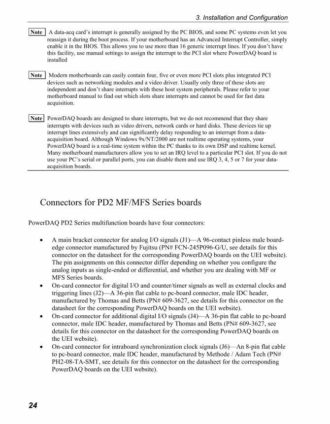
Connectors for PD2 MF/MFS Series boards
PowerDAQ PD2 Series multifunction boards have four connectors:
• A main bracket connector for analog I/O signals (J1)—A 96-contact pinless male board-
edge connector manufactured by Fujitsu (PN# FCN-245P096-G/U, see details for this
connector on the datasheet for the corresponding PowerDAQ boards on the UEI website).
The pin assignments on this connector differ depending on whether you configure the
analog inputs as single-ended or differential, and whether you are dealing with MF or
MFS Series boards.
• On-card connector for digital I/O and counter/timer signals as well as external clocks and
triggering lines (J2)—A 36-pin flat cable to pc-board connector, male IDC header,
manufactured by Thomas and Betts (PN# 609-3627, see details for this connector on the
datasheet for the corresponding PowerDAQ boards on the UEI website).
• On-card connector for additional digital I/O signals (J4)—A 36-pin flat cable to pc-board
connector, male IDC header, manufactured by Thomas and Betts (PN# 609-3627, see
details for this connector on the datasheet for the corresponding PowerDAQ boards on
the UEI website).
• On-card connector for intraboard synchronization clock signals (J6)—An 8-pin flat cable
to pc-board connector, male IDC header, manufactured by Methode / Adam Tech (PN#
PH2-08-TA-SMT, see details for this connector on the datasheet for the corresponding
PowerDAQ boards on the UEI website).

3. Installation and Configuration
25
Figure 3.7—Cable connection diagram for PowerDAQ MF (S) boards
Figure 3.8a—Physical layout of J1 / JA1 Connector on PD2 MF(S) Series boards
Fig 3.8a gives a view looking at the connector as mounted on the board.

3. Installation and Configuration
26
2
1
50
49
3 51
4 52
5 53
6 54
7 55
8 56
57
10 58
11 59
12 60
13 61
62
15 63
16 64
17 65
18 66
19 67
20 68
21 69
22 70
23 71
24 72
25 73
26 74
27 75
28 76
29 77
30 78
31 79
32 80
33 81
34 82
35 83
36 84
37 85
38 86
39 87
40 88
41 89
42 90
43 91
44 92
45 93
46 94
47 95
48 96
AGND
AGND
AGND
AGND
DGND
AGND
AIN55
AIN53
AIN51
AIN49
AGND
AIN38
AIN36
AIN34
AIN33
AIN23
AIN21
AGND
AIN18
AIN16
AIN6
AIN5
AIN3
AIN1
AGND
DSP Trigger Input/ AO External Clock
*ADC Conversion Start Out/ Pacer clock out
N/ C
AGND
ADC Channel List Start Input / Burst Clock
AIN62
AIN60
AIN59
AIN57
AIN47
AGND
AIN44
AIN42
AIN40
AGND
AIN29
AIN27
AIN25
AIN24
AIN14
AIN12
AGND
AIN9
AGND
AOUT0
AGND
AOUT1
AGND
AGND
AIN54
AIN52
AIN50
AIN48
AIN39
AIN37
AIN35
AGND
AIN32
AIN22
AIN20
AIN19
AIN17
AIN7
AGND
AIN4
AIN2
AIN0
AGND
+5V (100 mA max)
ADC Conversion Start Input / Pacer clock
AGND
N/ C
AIN63
AIN61
AGND
AIN58
AIN56
AIN46
AIN45
AIN43
AIN41
AIN31
AIN30
AIN28
AIN26
AGND
AIN15
AIN13
AIN11
AIN10
AIN8
Figure 3.8b—Pin assignments on J1 / JA1 Connector on PD2-MF boards, in single-ended mode
In Fig 3.8b, the * symbol means that the line is disconnected by default, consult factory if you
need this clock on the J1 connector.
3. Installation and Configuration
27
2
1
50
49
3 51
4 52
5 53
6 54
7 55
8 56
57
10 58
11 59
12 60
13 61
62
15 63
16 64
17 65
18 66
19 67
20 68
21 69
22 70
23 71
24 72
25 73
26 74
27 75
28 76
29 77
30 78
31 79
32 80
33 81
34 82
35 83
36 84
37 85
38 86
39 87
40 88
41 89
42 90
43 91
44 92
45 93
46 94
47 95
48 96
AGND
AGND
AGND
AGND
DGND
AGND
AIN55
AIN53
AIN51
AIN49
AGND
AIN38
AIN36
AIN34
AIN33
AIN23
AIN21
AGND
AIN18
AIN16
AIN6
AIN5
AIN3
AIN1
AGND
DSP Trigger Input/ AO External Clock
ADC Conversion Start Out/ Pacer clock out
N/ C
AGND
ADC Channel List Start Input / Burst Clock
AIN54 Return
AIN52 Return
AIN51 Return
AIN49 Return
AIN39 Return
AGND
AIN36 Return
AIN34 Return
AIN32 Return
AGND
AIN21 Return
AIN19 Return
AIN17 Return
AIN16 Return
AIN6 Return
AIN4 Return
AGND
AIN1 Return
AGND
AOUT0
AGND
AOUT1
AGND
AGND
AIN54
AIN52
AIN50
AIN48
AIN39
AIN37
AIN35
AGND
AIN32
AIN22
AIN20
AIN19
AIN17
AIN7
AGND
AIN4
AIN2
AIN0
AGND
+5V (100 mA max)
ADC Conversion Start Input / Pacer clock
AGND
N/ C
AIN55 Return
AIN53 Return
AGND
AIN50 Return
AIN48 Return
AIN38 Return
AIN37 Return
AIN35 Return
AIN33 Return
AIN23 Return
AIN22 Return
AIN20 Return
AIN18 Return
AGND
AIN7 Return
AIN5 return
AIN3 Return
AIN2 Return
AIN0 Return
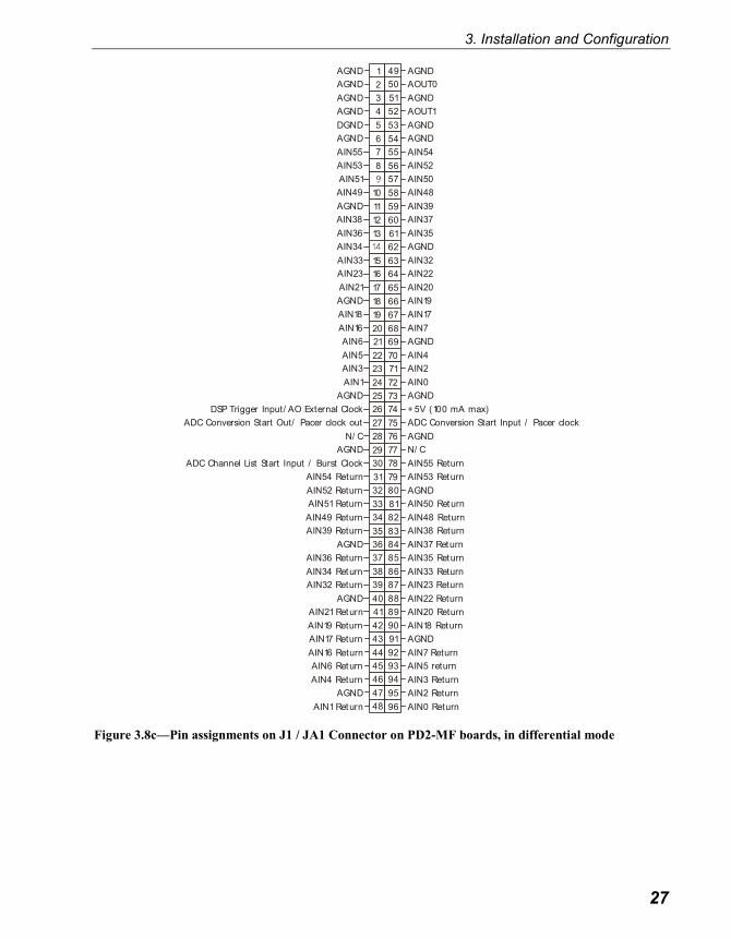
Figure 3.8c—Pin assignments on J1 / JA1 Connector on PD2-MF boards, in differential mode

3. Installation and Configuration
28
2
1
50
49
3 51
4 52
5 53
6 54
7 55
8 56
57
10 58
11 59
12 60
13 61
62
15 63
16 64
17 65
18 66
19 67
20 68
21 69
22 70
23 71
24 72
25 73
26 74
27 75
28 76
29 77
30 78
31 79
32 80
33 81
34 82
35 83
36 84
37 85
38 86
39 87
40 88
41 89
42 90
43 91
44 92
45 93
46 94
47 95
48 96
AGND
AGND
AGND
AGND
DGND
AGND
AGND
AGND
AGND
AGND
AGND
AGND
AGND
AGND
AGND
AGND
AGND
AGND
AGND
AGND
AIN6
AIN5
AIN3
AIN1
AGND
DSP Trigger Input/ AO External Clock
ADC Conversion Start Out/ Pacer clock out
-12V
AGND
ADC Channel List Start Input / Burst Clock
AGND
AGND
AGND
AGND
AGND
AGND
AGND
AGND
AGND
AGND
AGND
AGND
AGND
AGND
AIN6 Return
AIN4 Return
AGND
AIN1 Return
AGND
AOUT0
AGND
AOUT1
AGND
AGND
AGND
AGND
AGND
AGND
AGND
AGND
AGND
AGND
AGND
AGND
AGND
AGND
AGND
AIN7
AGND
AIN4
AIN2
AIN0
AGND
ADC Conversion Start Input / Pacer clock
AGND
+12V
AGND
AGND
AGND
AGND
AGND
AGND
AGND
AGND
AGND
AGND
AGND
AGND
AGND
AGND
AIN7 Return
+5V (100 mA max)
AIN5 Return
AIN3 Return
AIN2 Return
AIN0 Return
Figure 3.8d—J1 / JA1 Connector on PD2-MFS boards, single-ended or differential modes
3. Installation and Configuration
29
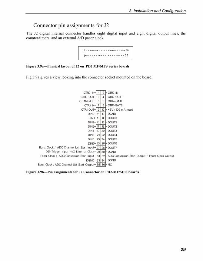
Connector pin assignments for J2
The J2 digital internal connector handles eight digital input and eight digital output lines, the
counter/timers, and an external A/D pacer clock.
Figure 3.9a—Physical layout of J2 on PD2 MF/MFS Series boards
Fig 3.9a gives a view looking into the connector socket mounted on the board.
1 2
3 4
5 6
7 8
9 10
11 12
13 14
16
17 18
19 20
21 22
23 24
26
27 28
29 30
31 32
33 34
35 36
CTR0-IN
CTR0-OUT
CTR0-GATE
CTR1-IN
CTR1-OUT
DIN0
DIN1
DIN2
DIN3
DIN4
DIN5
DIN6
DIN7
Burst Clock / ADC Channel List Start Input
Pacer Clock / ADC Conversion Start Input
DGND
Burst Clock / ADC Channel List Start Output
CTR2-IN
CTR2-OUT
CTR2-GATE
CTR1-GATE
+5V (100 mA max)
DGND
DOUT0
DOUT1
DOUT2
DOUT3
DOUT4
DOUT5
DOUT6
DOUT7
DGND
ADC Conversion Start Output / Pacer Clock Output
DGND
NC
Figure 3.9b—Pin assignments for J2 Connector on PD2-MF/MFS boards

3. Installation and Configuration
30
Connector pin assignments for J4
The J4 Connector handles an additional eight digital-input and eight digital-output lines on boards
with these extra DIO features.
Figure 3.10a—Physical layout of J4 on PD2 MF/MFS Series boards
Fig 3.10a gives a view looking into the connector socket mounted on the board.
1 2
3 4
5 6
7 8
9 10
11 12
13 14
16
17 18
19 20
21 22
23 24
26
27 28
29 30
31 32
33 34
35 36
DGND
DGND
DGND
DGND
DGND
DIN8
DIN9
DIN10
DIN11
DIN12
DIN13
DIN14
DIN15
DGND
DGND
DGND
DGND
DGND
DGND
DGND
DGND
DGND
+5V (100 mA max)
DGND
DOUT8
DOUT9
DOUT10
DOUT11
DOUT12
DOUT13
DOUT14
DOUT15
DGND
DGND
DGND
DGND
Figure 3.10b—Pin assignments for J4 Connector on PD2-MF/MFS boards
3. Installation and Configuration
31
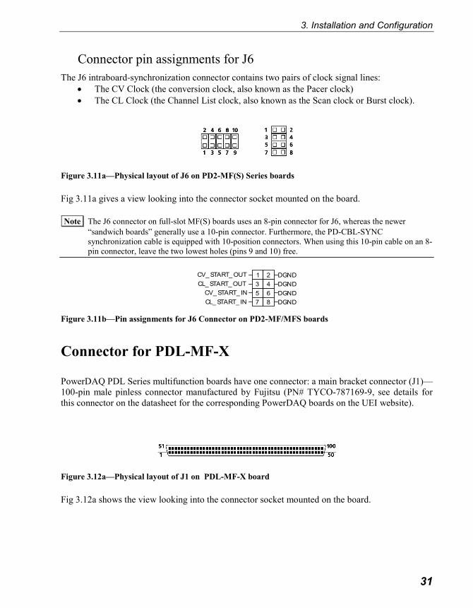
Connector pin assignments for J6
The J6 intraboard-synchronization connector contains two pairs of clock signal lines:
• The CV Clock (the conversion clock, also known as the Pacer clock)
• The CL Clock (the Channel List clock, also known as the Scan clock or Burst clock).
Figure 3.11a—Physical layout of J6 on PD2-MF(S) Series boards
Fig 3.11a gives a view looking into the connector socket mounted on the board.
Note The J6 connector on full-slot MF(S) boards uses an 8-pin connector for J6, whereas the newer
“sandwich boards” generally use a 10-pin connector. Furthermore, the PD-CBL-SYNC
synchronization cable is equipped with 10-position connectors. When using this 10-pin cable on an 8-
pin connector, leave the two lowest holes (pins 9 and 10) free.
1 2
3 4
5 6
7 8
CV_START_OUT
CL_START_OUT
CV_START_ IN
CL_START_ IN
DGND
DGND
DGND
DGND
Figure 3.11b—Pin assignments for J6 Connector on PD2-MF/MFS boards
Connector for PDL-MF-X
PowerDAQ PDL Series multifunction boards have one connector: a main bracket connector (J1)—
100-pin male pinless connector manufactured by Fujitsu (PN# TYCO-787169-9, see details for
this connector on the datasheet for the corresponding PowerDAQ boards on the UEI website).
Figure 3.12a—Physical layout of J1 on PDL-MF-X board
Fig 3.12a shows the view looking into the connector socket mounted on the board.
3. Installation and Configuration
32
AIN8
AGND
AIN9
AGND
AIN10
AGND
AIN11
AGND
AIN12
AGND
AIN13
AGND
AIN14
AGND
AIN15
AGND
AOUT0
AGND
DIN1
DIN3
DIN5
DIN7
DIN9
DIN11
DIN13
DIN15
DGND
DIN17
DIN19
DIN2 1
DIN23
DOUT1
DOUT3
DOUT5
DOUT7
DGND
DOUT9
DOUT11
DOUT13
DOUT15
DOUT17
DOUT19
DOUT2 1
DOUT23
DGND
EXT_TRIG_ IN
CV_OUT
EXT_ TRIG_OUT
CL_OUT
EXT_CLOCK
AIN0
AGND
AIN1
AGND
AIN2
AGND
AIN3
AGND
AIN4
AGND
AIN5
AGND
AIN6
AGND
AIN7
EXT_ GND
AOUT1
AGND
DIN0
DIN2
DIN4
DIN6
DIN8
DIN10
DIN12
DIN14
DGND
DIN16
DIN18
DIN20
DIN22
DOUT0
DOUT2
DOUT4
DOUT6
+ 5VPJ2
DOUT8
DOUT10
DOUT12
DOUT14
DOUT16
DOUT18
DOUT20
DOUT22
DGND
TMR2
DGND
TMR1
DGND
TMR0
10
20
30
40
2
1
3
4
5
6
7
8
9
11
12
13
14
15
16
17
18
19
21
22
23
24
25
26
27
28
29
31
32
33
34
35
36
37
38
39
41
42
43
44
45
46
47
48
49
50
51
52
53
54
55
56
57
58
59
60
61
62
63
64
65
66
67
68
69
70
71
72
73
74
75
76
77
78
79
80
81
82
83
84
85
86
87
88
89
90
91
92
93
94
95
96
97
98
99
100
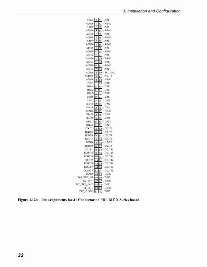
Figure 3.12b—Pin assignments for J1 Connector on PDL-MF-X Series board

3. Installation and Configuration
33
Connectors for PDXI MF(S) Series boards
PowerDAQ PDXI-MF(S) Series multifunction boards have two connectors:
• A main bracket connector for analog I/O signals (J1)—A 96-contact pinless male
connector manufactured by Fujitsu (PN# FCN-245P096-G/U, see details for this
connector on the datasheet for the corresponding PowerDAQ boards on the UEI website).
Note The connector pinout for J1 on the PDXI MF/MFS Series is identical to the pinouts on the PD2-
MF/MFS Series. See Figures 3.8a-d
• On-card connector for digital I/O and counter/timer signals (J2)—An 80-pin flat cable to
pc-board connector, male IDC header, manufactured by Methode/Adam Tech (PN#
HBMR-A-80-VSG, see details for this connector on the datasheet for the corresponding
PowerDAQ boards on the UEI website).
Figure 3.13—Cable connection diagram for PDXI-MF(S) boards
Figure 3.14a—Physical layout of J2 on PDXI-MF/MFS Series boards
Fig 3.14a gives a view looking into the connector socket mounted on the board.

3. Installation and Configuration
34
DOUT11
DIN13
DOUT12
DIN14
DOUT13
DIN15
DOUT14
DOUT15
DGND
DGND
DGND
DGND
DGND
DGND
DGND
DGND
DGND
DGND
DGND
DGND
DGND
DGND
DGND
DGND
DGND
DGND
DGND
DGND
DGND
DGND
DGND
DGND
DGND
UCT0_CLK_ IN
UCT2_CLK_ IN
UCT0_OUT
UCT2_OUT
UCT0_GATE
UCT2_GATE
UCT1_ CLK_ IN
DIN12
DOUT10
DIN11
DOUT9
DIN10
DOUT8
DIN9
DGND
DIN8
+5VPJ2
DGND
CL_DONE_OUT
CL_START_OUT_BACK
DGND
DGND
CL_START_OUT
CL_START_ IN_BACK
DGND
TRIG_ IN_BACK
DOUT7
CL_START_ IN_BACK
DOUT6
DIN7
DOUT5
DIN6
DOUT4
DIN5
DOUT3
DIN4
DOUT2
DIN3
DOUT1
DIN2
DOUT0
DIN1
DGND
DIN0
+5VPJ2
UCT1_OUT
UCT1_GATE
3
1
5
7
9
11
13
15
19
21
23
25
29
31
33
35
37
39
41
43
45
47
49
51
53
55
57
59
61
63
65
67
69
71
73
75
77
79
2
4
6
8
10
12
14
16
18
20
22
24
26
28
30
32
34
36
38
40
42
44
46
48
50
52
54
56
58
60
62
64
66
68
70
72
74
76
78
80
Figure 3.14b—Pin assignments of J2 Connector on PDXI MF/MFS Series boards
The PXI_TRIG 0…7 and PXI_STAR lines on the PXI system backplane (located on Connector
P2, above Connector P1) can be used for interboard synchronization.

3. Installation and Configuration
35
“Simple Test” program
After wiring external signals to your PowerDAQ board, run the PowerDAQ Simple Test program
to verify that all subsystems are operating properly.
From the Start menu, select Programs PowerDAQ Simple Test, and the utility’s dialog
box appears.
Figure 3.15—Simple Test application
Use the Analog In, Analog Out, Digital In, Digital Out and Counters tabs to observe your
application running on the board. From these pages you can control the mode (single-ended or
differential), range, gain, number of channels activated and the channel whose value appears on
the screen.
It’s often helpful to run an analog I/O loopback test with the help of this utility. First wire AOut0
to all even-numbered AIn channels and then wire AOut1 to all odd-numbered AIn lines. Be sure to
increase the number of active channels in the AnalogIn tab to the maximum, and click Start. Now
go to the AnalogOut tab, select two different waveforms for the two active channels and click
Start. Return to the AnalogIn tab and scroll through various channels to verify the operation of
each.
You can similarly run a digital I/O loopback test. Wire Dout channels to corresponding Din
channels. Click Start on the DigitalOut tab, then return to the DigitalIn tab and verify the operation
of each line.

3. Installation and Configuration
36
Calibration
All PowerDAQ hardware ships fully calibrated and do not require additional calibration on the
part of the user. The boards store calibration values for each range and each gain in EEPROM.
When you initially load the PowerDAQ board driver and configure the analog-input subsystem,
that process loads the calibration values from EEPROM.
However, to ensure peak performance from your PowerDAQ hardware, we suggest that a
PowerDAQ board be recalibrated every 12 months.

37
4. PowerDAQ
Architecture
Functional Overview
The PowerDAQ MF/MFS Series features extensive input modes, clocking and triggering
capabilities. It also provides simultaneous subsystem operation.
+
-
External Analog I/O Connector
(64)
DAC0
DAC1
VoltageReference
AOut CalibrationDACs
AnalogOutput
Amplif iers
Ext. Aln Conv Clock
Ext. Aln Scan Clock
Ext. Trigger
Aln Clock Out
Aln Control
Bus Master PCI Interface
Motorola 66MHz DSP 56301
ESSI
AOut FIFO
AOut Clock
6 Channel
DMA
12k Program
RAM
12k Data RAM
Bootstrap
ROM
Aln Conv
Clock
Aln Scan
Clock
VoltageReference
Aln CalibrationDACs
CustomPGIA GainAmp.
12,14,16-bit
SamplingA/ D
Converter
Upgradable1k SampleADCFIFO
Channel/GainControlLogic
ChannelListFIFO
Aln PowerConditioner
16 or 64ChannelAnalog
Multiplexer
DigitalOutput(Driver)
Conf iguration& CalibrationEEPROM
32 Bit PCI Bus
Control
Address
Data
(16)
Internal Digital I/O Connectors J2,J4
(16)
Interboard Synchronization
DigitalInput
Buf fer
Latch
Interrupt
(4)
UCT Control
DIn Control
DOut Control
AIn Clocking & Triggering
Address
Ext. Aln Conv Clock
Ext. Aln Scan Clock
Ext. Trigger
Aln Clock Out
Clock
Gate
Out
3
3
3
UserCounterTimer
(82C54)
Local Data Bus
Figure 4.1—PowerDAQ PD2-MF/MFS Series block diagram

4. PowerDAQ Architecture
38
+
-
External Analog I/O Connector
(64)
PowerDAQ II
Data Acquisit ionControl and
Timing Logic
DAC0
DAC1
Voltage
Refere nce
AOut Calib rat ion
DACs
Analog
OutputAmplif iers
Ext. Aln Conv Clock
Ext. Aln Scan Clock
Ext. Trigger
A ln Clock Out
Aln Con t rol
Bus Mast er PCI Int erface
Motorola 66MHz DSP 56301
ESSI
AOut FIFO
AOut Clock
6 Channel
DMA
12k Program
RAM
12k Data RAM
Bootstrap
ROM
Aln Conv
Clock
Aln Scan
Clock
Volt ageRef e rence
Aln Calibration
DACs
Cust omPGIA GainAmp.
12,14 ,16-bit
Sampling
A/ DConvert er
Upgradable1k Sample
ADCFIFO
Channel/Gain
ControlLogic
ChannelLi stFIFO
Aln PowerCond itioner
16 or 64ChannelAnalog
Mult iplexer
Digit al
Outp ut(Drive r)
Con f igurat ion& Calibrat ionEEPROM
PXIControlLogic
32 Bit CompactPCI Bus PXI
(16)
Internal Digital I/O Connector J2
(16)
Digit alInput
Buf f e r
Latch
Int erru pt
UCT Contro l
DI n Control
DOut Cont rol
Clock ing & Tr ig gering Lin es
Address
Ext. Aln Conv Clock
Ext. Aln Scan Clock
Ext. Trigger
A ln Clock Out
Clock
Gate
Out
3
3
3
Use rCount erTimer
(82C54)
Local Da ta Bus
Control
Address
Data
Figure 4.2—PowerDAQ PDXI-MF/MFS Series block diagram

4. PowerDAQ Architecture
39
+
-
PowerDAQ IIDat a Acquisit ionControl and
Timing Logic
DAC0
DAC1
Volt ageReferen ce
AOut Calibrat ionDACs
AnalogOutput
Amplif iers
Ext. A
ln Conv Clock
Ext. T
rigger
Remoute Ground
Aln Clock Out
Aln Con t rol
External Analo g/ Digital I/ O Connector
Volt ageRefe rence
Aln CalibrationDACs
PGIAGainAmp.
16-bitSampling
A/ DConverter
Upgradable1k Sample
ADCFIFO
Ch annel/Gain
ControlLogic
Aln PowerCond itioner
(3)
(24)
(16)
(24)
16 ChannelAnalog
Mu ltiplexer
Conf iguration& Calibrat io nEEPROM
32 Bit PCI Bus
UCT Contro l
DIn Con t rol
DOut Cont rol
DSPCou nterTi mer
Control
Address
Data
DSPChannel List
FIFO
Local Da ta Bus
Address
Digit alInput
Buf f er
Latch
Bus Mast er PCI Int erf ace
Motorola 66MHz DSP 56301
ESSI
AOut FIFO
AOut Clock
6 Channel
DMA
12k Program
RAM
12k Data RAM
Bootstrap
ROM
Aln Conv
Clock
Aln Sca
nClock
Digit al
Out put(Driver)
Figure 4.3—PowerDAQ PDL-MF block diagram
The heart of each board in the MF/MFS Series is a Motorola 56301, a 66-MHz DSP. That device
ensures a highly efficient interface with the PCI/PXI bus, and it also provides control over all
board subsystems.
The Analog Input subsystem includes:
• An input multiplexer (Mux) selects which channels to acquire. The Channel List FIFO
contains a list of each channel to be acquired along with its gain; the subsystem reads this
data and sets up the input mux accordingly. PD2-MFS boards have per-channel sample/
hold amplifiers (S/Hs) preceding the mux. The S/Hs acquire a signal from all input
channels simultaneously and then hold the acquired voltages while the A/D digitizes
them channel-by-channel.
• A Programmable Gain Amplifier (PGA) increases the level of an input signal in order to
provide an adequate voltage to the A/D. The PGA’s level of amplification depends on the
board model and can be software selected on a per-channel basis. Models in the MF
4. PowerDAQ Architecture
40
Series come with one of two sets of amplification levels. For low-level signals that need
considerable boosting, select the /L option (G = 1, 10, 100 or 1000); for high-level
signals that don’t require as much amplification, select the /H option (G = 1, 2, 4 or 8).
The PDL-MF board ships two versions, both with G = 1, 2, 5 or 10. MFS Series boards
ship standard only with unity gain; for other gains (G = 1, 2, 5 or 10 you must purchase
the –DG option).
• An A/D FIFO holds digitized samples until the DSP transfers them into host memory
over the PCI/PXI bus. The default A/D FIFO size starts at 1k samples and depending on
the board model can be as large as 4k samples. You can upgrade the FIFO to 16k, 32k or
64k samples depending on application requirements. Note that while larger FIFOs
achieve smoother operation, especially at high acquisition rates, there is a tradeoff in
terms of response time. Specifically, the driver normally transfers data from the buffer
only when the FIFO is half full, so a larger buffer means you wait longer for a transfer.
This extra time can degrade system response in closed-loop control applications.
• A calibration D/A generates voltages to adjust the offset and gain settings on the analog-
input section to ensure accurate performance. As noted in the previous section, all boards
are factory calibrated for each input range and mode.
• The timing, triggering and clocking controls allow you to select the timebase, clock and
triggering sources, a “slow bit” and other options.
• An interrupt mechanism notifies the DSP of special conditions on this subsystem so the
user application can take appropriate action.
The Analog Output subsystem includes:
• A DSP-based FIFO that holds as many as 2k samples of digitized waveform values to
feed to the output D/A.
• A 12-bit D/A that converts digitized waveform values into analog output voltages.
• A calibration D/A that provides voltages to adjust offset and gain on the analog output to
ensure accurate performance.
• Timing, triggering and clocking controls that allow you to select the analog-output rate
and clock source.
• An interrupt mechanism that notifies the DSP of special conditions on this subsystem so
the user application can take appropriate action.
The Digital Input/Output subsystem includes:
• A 16-bit register to read logic levels on digital input lines (24-bit register on PDL-MF).
• An 8-bit Schmidt trigger to catch logic-level changes on digital input lines (not present on
PDL-MF).

4. PowerDAQ Architecture
41
• A 16-bit register to hold logic levels on digital output lines once the program has written
data to the outputs (24-bit register on PDL-MF).
• An interrupt mechanism notifies the DSP of special conditions on this subsystem so the
user application can take appropriate action.
The User Counter/Timer subsystem includes:
• Three 16-bit Intel 82C54 counter timers, fully accessible by the user (the counter/timers
on the PDL-MF are shared with the 24-bit DSP 56301).
• Clock-source selection and control logic.
• Gate-source selection and control logic.
• An interrupt mechanism notifies the DSP of special conditions on this subsystem so the
user application can take appropriate action.

4. PowerDAQ Architecture
42
Programming Model
No matter which subsystem you choose to work with, the way you initialize and set up the board
is very much the same, so before digging into details of individual subsystems it makes sense to
review these general procedures.
An onboard DSP controls all subsystems. User applications communicate with the board via the
PowerDAQ API, which is integrated into the PowerDAQ dynamic-link library (DLL). To inform
an application about hardware events, the driver creates kernel events. Data is transferred from the
board through the PCI bus and stored in the user-level buffer. The PowerDAQ API includes a set
of information functions that allow user applications to get board-specific information, such as
model, serial number and IRQ line.
Figure 4.4—Communication between a user application and a PowerDAQ multifunction board

4. PowerDAQ Architecture
43
Programming subsystems
All PowerDAQ subsystems have two modes of operation:
• Polled
• Event-based
In Polled mode, the user application queries the board about the status of various subsystems as
needed. This method is preferred when the application does not need to be notified about hardware
events. In Event-based mode, the board notifies the user application of certain predefined
subsystem events using Win32 calls. With this mode you can write truly asynchronous
applications.
Opening a subsystem
Before starting any board operations whatsoever, you must first open the driver, open the adapter
(another term that refers to a specific board), and acquire the subsystem. After completion of a
specific task the user application can release the subsystem, and when the application has
completed its work make sure it closes the adapter and driver.
This manual explains the general procedures for creating a program and important API calls. The
following calls outline the sequence you must make when programming under Win32; in
particular, the calls to open/close the driver and open/close the adapter are specific to Windows.
The remaining calls are valid for any OS.
For details on various functions and their calling parameters, see the PowerDAQ Programmer
Manual. The specific calls and their names might vary with other operating systems, so once again
you might want to refer to that manual.
API calls required for opening/closing a subsystem
• _PdDriverOpen(…)
Open the driver
• _PdAdapterOpen(…)
Open the adapter; only one process can open a given adapter at a time. This
function returns phAdapter, a handle for the adapter, and you will need this
variable in many later functions.
• _PdAcquireSubsystem(…)
Acquire the named subsystem for use (if you set dwAcquire = 1), and the
parameter dwSubsystem can be one of the following (as defined in typedef enum

4. PowerDAQ Architecture
44
_PD_SUBSYSTEM): AnalogIn, AnalogOut, DigitalIn, DigitalOut,
CounterTimer.
… let the user app work with the subsystem, then …
• _PdAcquireSubsystem(…)
Release the subsystem from use (if you set dwAcquire = 0)
• _PdAdapterClose(…)
Close the adapter
• _PdDriverClose(…)
Close the drive

45
5. Analog-Input
Subsystem
Architecture
The analog-input subsystem consists of an A/D converter, signal-conditioning circuitry and
control of other front-end devices such as a multiplexer or multiple sample/hold amplifiers. The
subsystem’s first stage multiplexes raw signals from the input channels into a successive-
approximation A/D with a resolution of 12, 14 or 16 bits. The A/D subsystem also includes
selection of input mode (single-ended or differential), polarity, gain settings, range settings, set up
of the Channel List, trigger and clocking control.
The multiplexer on MF boards is located at the signal inputs and can be switched to function either
in single ended (SE) or differential (DI) mode (Fig 5.1). The selected mode is applied to all input
channels. The output of the mux feeds an instrumentation amplifier and then the signal goes into a
custom programmable gain amplifier (PGA). Channel numbers, along with their gains, are stored
in a Channel List. With this mechanism you can select the order in which the channels are read as
well as set different gains on a per-channel basis.
Input Ranges
The majority of PowerDAQ boards feature four possible input ranges, which are applied globally
across all input channels and are applied to all signals. You select the input mode (SE/DI) and
range from Table 5.1 with the _PdAInSetCfg() command.
Unipolar Bipolar
0-10V ±10V
0-5V ±5V
Table 5.1—PowerDAQ analog-input ranges
Note The only exception to this table is the PDL-MF, which does not offer the 0-5V range.

5. Analog-Input Subsystem
46
Gain Settings
You can set a gain for each channel on an MF/MFS Series board prior to acquisition, and you do
so by setting up a Channel List as described in the next section. There are three gain ranges. In
Table 5-2 below, the “L” or “H” appears at the end of the model number as appropriate (such as
PD2-MF-64-2M/14L) and applies to the MF Series boards only. An “L” indicates that a board is
appropriate for working with low-level signals that need a large gain. An “H” indicates that a
board is appropriate for high-level signals that need less gain. The PDL-MF boards and the
standard MFS Series are available only with one set of gains.
MF Series “L” Suffix
MF Series “H” Suffix Preselected gains on
PDL-MF or options
for MFS Series cards
G = 1, 10, 100, 1000 G = 1, 2, 4, 8 G = 1, 2, 5, 10
Table 5.2—Programmable Gains
Channel List
Often you want to sample only over a certain subset of channels, sample them in various orders or
apply different gains to each channel. These options are all possible with an A/D Channel List,
which you create with the _PdAInSetChList() command. It is mandatory that you create a channel
list, otherwise the board will not collect the correct data.
The Channel List is resident in the on-card memory known as the Channel List FIFO and thus
must be programmed every time you power up the card. It contains from one to 256 entries (64
entries maximum on the PDL-MF). Each reading of the full list is called a scan. Configuration
data for each entry includes the channel number, gain, and Slow Bit setting. A Channel List
remains active until you overwrite it with a new set of entries. Writing a Channel List with 0
entries clears the list
To effectively change the sampling rate of just one channel, make multiple entries for it
in the Channel List instead of reading it just once per scan.
You can use averaging over several scans to increase the effective resolution and reduce
noise. For applications where the dc value is crucial, consider using a software filter that
consists of an averaging window over an array of averages. Each time you calculate the
average value of a channel you put it into an array, and if that array is already full you
replace the oldest one. Then your program calculates the average value of the array of
averages and uses it as a final value.
Giving you added flexibility in setting up a Channel List is the Slow Bit feature. It is a special
marker you can activate in every channel, and it instructs the analog front end to insert a delay in
the acquisition sequence, thus allowing the input amplifier to settle before it clocks the A/D to
make a conversion. This feature is useful if you are applying a high gain (100 or 1000) to a signal.
TIP
TIP

5. Analog-Input Subsystem
47
With a Slow Bit you can give that channel extra time without slowing down all the others. Be
aware, though, that turning on the Slow Bits can result in a reduction in a board’s maximum
throughput rate.
The amount of delay due to a Slow Bit varies with each PowerDAQ model. A table giving the
minimum time between conversions you can expect with any particular model with the Slow Bit
active appears in Appendix B.
The Channel List has the following format:
Bit 8 Bits 7, 6 Bits 5-0
Slow bit
(0 = Off
1 = On)
Gain
(see Table 5.3b)
Channel to acquire
(000000 = Ch 0
111111 = Ch 63)
Table 5.3a—Channel List format
Gain coding
(Bits 7, 6)
“L” Gains
(MF Series)
“H” Gains
(MF Series)
Gains for MFS
and PDL-MF
boards
00 1 1 1
01 10 2 2
10 100 4 5
11 1000 8 10
Table 5.3b—Programmable-gain codes
Input modes
The analog-input section on all PowerDAQ boards multiplexes the active input channels into a
single 12-, 14- or 16-bit successive approximation A/D. The boards can be configured to work
with either single-ended (16 to 64) or differential (8 to 32) inputs, and the selected mode must be
the same for all channels.
This selection of input mode can lead to some confusion. No matter what the underlying test-
system configuration, all voltage measurements are made between two points and thus are
inherently differential. One node is at a potential as compared to the level on the other input
terminal, and that level can be at a ground reference or at an elevated voltage level. On a PC-based
data-acq card, one line of the input amplifier is always connected to the signal of interest. To what
level the second (referenced) line on the input amp is connected determines in which of three
possible input modes the amp is operating.
• Single-ended channels refer all their inputs to a common ground that is also connected to
the computer ground.
• Pseudodifferential channels refer all their inputs to a common ground—but this ground
is not connected to the computer ground.

5. Analog-Input Subsystem
48
• Differential inputs use an independent reference for each channel, and these references
are not connected to the computer ground (and instead are generally a return path directly
to the source of the signal being digitized).
Each mode has its strengths and weaknesses, so you should pay close attention to the connection
on the input’s reference terminal.
Note No matter whether you choose single-ended, pseudodifferential or differential mode, be sure to short
unused channels to ground using a 1 kΩ to 10-kΩ resistor.
Signal Source Type
Floating Signal Source (Not connected to ground)
Grounded Signal Source
Input configuration
Examples
• Thermocouples
• Signal Conditioning with Isolated Outputs
• Battery Devices
Examples
• Plug-in instruments with Non-isolated Inputs
Differential
Two resistors (10kΩ < R < 100kΩ) provide return paths to ground for
bias currents; In most cases R* is optional
Single-Ended Ground
Referenced
Table 5.3c—Analog Input Configurations

5. Analog-Input Subsystem
49
Single-ended
A PowerDAQ card operating in single-ended mode (Fig 5.1) digitizes across as many as 64
channels. For single-ended inputs you connect one wire from each signal source to the High input
of the data-acq system’s input amplifier, and all signals share a common return path connected to
analog ground (AGND). You should connect this common return path to both a ground near the
signal source and also to the ground on the PC, which in this way gets set at the same level as the
signal ground.
Pseudodifferential
The PDL-MF card allows operation in pseudodifferential mode (Fig 5.1). For pseudodifferential
inputs you connect one wire from each signal source to the High input of the data-acq system’s
input amplifier, and all signals again share a common return path to AGND. However, this ground
signal is typically referenced to a remote source and it is separated from the PC ground; thus it can
float at a different level. The maximum difference between common ground and PC ground
should never exceed 10V. You can remove the effect of this voltage offset from measurement
results by subtracting the difference between AGND and COM from the measured result. Because
the AGND line in a pseudodifferential setup is not connected to the computer ground, it is not
subject to the associated digital noise within the PC.
Figure 5.1—Wiring for single-ended and pseudodifferential inputs
Differential
A PowerDAQ card operating in differential mode digitizes across as many as 32 channels. Each
channel uses two lines on the data-acquisition system’s input amplifier (Fig 5.2)—you connect
one lead from the signal source to the channel’s High input (the positive input of the amp) and

5. Analog-Input Subsystem
50
connect the other signal lead to the channel’s Low input (the amp’s negative input). Each signal
floats at its own level without any reference to ground or other inputs.
For example, when working with a 16-channel PowerDAQ board in differential mode, Ch 0 and 8
form the High and Low inputs of differential-input Ch 0; next, for differential-input Ch 1 you use
Ch 1 and 9; follow this pattern for all eight differential-input pairs. Follow this procedure when
wiring the PDL-MF board according to the pin assignments in Fig 3.12b. However, we have
prepared separate differential-input pin-assignment diagrams for the PD2/PDXI-MF(S) boards,
and they appear in Figs 3.8c and 3.8d.
The voltage between the inputs and the PC ground is monitored by two high-impedance
amplifiers. A third amplifier measures the difference between the Positive and Negative inputs,
eliminating any voltage common to both wires. This method eliminates problems that can arise
with a single-ended system because this configuration attenuates noise common to both channel
inputs (common-mode noise). Thus it’s wise to use twisted-pair cable to bring signals to the data-
acq card because that setup ensures that any noise generated along the wiring path is the same for
each line, and this noise gets subtracted by the amplifier.
Although using differential inputs on MF Series and PDL-MF boards cuts in half the number of
channels you can read with a given data-acq card compared to single-ended or pseudodifferential
setups, there are several cases where you are well advised to use differential inputs:
• when signal leads are over a few meters in length, because the instrumentation amp can
eliminate the effect of noise pickup from signal leads and also eliminate the possibility of
ground differentials.
• when measuring signals less than approximately 100 mV, because such low-level signals
can otherwise be easily overwhelmed by noise and ground differentials that only the
differential mode can remove.
• when measuring the output from high-impedance sensors such as strain gauges, because
their high impedances can lead to higher common-mode voltages, which the differential
inputs are able to remove thus leading to higher resolution.
Figure 5.2—Wiring for differential inputs
In the pin-assignment of Fig 3.8c, AIn8 has the name AIn0Return, while AIn9 has the designation
AIn1Return)

5. Analog-Input Subsystem
51
Note Do not drive positive and negative differential inputs with voltages that exceed a value of AGND ±
14V; otherwise, the input multiplexers could lock up and even be damaged. Always connect
equipment grounds together in a star configuration with low resistance.
Overall Recommendations
In summary, when wiring applications the analog-input subsystem, keep the following factors in
mind:
• Pseudodifferential inputs cannot eliminate the effects of noise.
• Use differential inputs when working in an environment with electrical noise or when
using gains to amplify the raw signal.
• Use individually shielded twisted-pair wires between the sensor and the terminal panel
and also connect the shield to analog ground when working in an environment with
electrical noise.
• Run signal lines near devices that create high levels of electrical noise through a metal
cable tray above or below the work area.
• Keep wiring paths or conduits carrying power lines and signal lines physically separate.
• Never put signal cables in the same wiring harness as high-current or high-voltage cables.
• Avoid routing signal and power cables together in parallel paths unless a reasonable
distance separates the paths, reasonable being determined by the strength of the power
signals and the amount of shielding.
• Be aware that many external factors—among them power lines, poorly designed video
monitors or switching power supplies, solenoids, electric arcs from circuit breakers or
welders, and unshielded signal cables—can have a negative impact on the accuracy of
your measurements.
• Single-ended inputs are appropriate when you need to measure a large number of signals
but you also need to keep system costs to a minimum—and you are confident that the
above noise-inducing situations can be avoided.
Note Input multiplexers have a high input impedance. It is highly recommended that you ground all unused
channels using a 1-kΩ to 10-kΩ resistor. Further, try to use signal sources with a low output
impedance (<100Ω) to avoid crosstalk. To limit signal bandwidth, you can also place a capacitor on
the screw-terminal panel between the signal and ground (single-ended mode) or for differential mode
between signal and return lines. The suggested capacitor values are between 1000 pF and 0.047 µF
depending on the input frequency and the impedance of the signal source according to F = 1 /
(2πRC).
5. Analog-Input Subsystem
52
Sequential vs simultaneous sampling
Users have several choices in determining the relationship of one sample to the next: You can
sample a series of signals sequentially, and you can simulate simultaneous sampling by sampling
adjacent signals at the highest possible rate to minimize the time skew among them
(pseudosimultaneous); both of those methods are possible with MF Series boards. For true
simultaneous sampling where you must eliminate time skew among multiple channels, the best
solution is to work with MFS Series boards. The fact that all MFx boards use one A/D converter
determines their front-end architecture ahead of the converter.
Sequential sampling
For sequential sampling, a multiplexer feeds signals to a common input amplifier, which then
feeds the A/D converter (Fig 5-3). Clearly, the front end needs some time to switch from one input
to the next and allow the amplifier time to settle. In the MF Series cards there is very little
difference between the time the multiplexer switches to a new signal—when the front end sees a
new signal—and when that new signal is digitized.
On MF and PDL-MF Series boards the minimum delay between each channel readings is limited
by the rated speed of the board, which you can calculate as 1/rate. For instance, for a board rated at
2.2M samples/sec, the interchannel digitization delay is 1 / 2.2 x 106 = (1 x 10
-6 ) / 2.2 = 450 nsec.
By selecting a card with a fast front end (such as UEI cards that operate at megahertz speeds) and
collecting samples as quickly as possible, the delay between samples (ie, the time between t0, t1, t2
and so on) can be extremely short. If the input signal’s frequency is relatively low (5-10 times
lower than the acquisition rate), the difference in the acquired signal level from one sample to the
next is minimal. For many applications, especially where the signals you are measuring change
slowly, this interchannel delay is so small that you can consider the samples to be virtually
simultaneous. This is also referred to as pseudosimultaneous operation.
If you are interested in phase differences between channels, an MFS board is more
suitable for such an application.
TIP

5. Analog-Input Subsystem
53
Figure 5.3a—Analog front end of a PowerDAQ MF Series board
In Fig 5.3b, CL refers to the CL Clock, also known as the Channel List clock or the Scan Clock.
CV refers to the CV Clock, also known as the Conversion Clock.
Figure 5.3b—Acquisition sequence for multiplexed inputs on MF Series and PDL boards
Note that t1 shows the time between individual samples on the A/D; the time between CV clocks is
limited by the board’s maximum digitization rate. If you need to increase the settling time between
samples, slow down the board by decreasing its digitization rate.

5. Analog-Input Subsystem
54
Next, ts is the minimal time between scans of the Channel List; it depends on t1 and the number of
entries in the Channel List. The value of 1 / ts is the maximum scan rate (in Hz). If the board is set
up such that the CL Clock comes before the board is ready to accept a new scan, the board ignores
the clock and sets an Error bit.
Note When driven with the internal clock, the preferred configuration for MF Series boards is CL =
continuous and CV = internal. For MFS Series boards, the preferred configuration is the reverse,
specifically, CL = internal and CV = continuous (see following section on clocking).
The effective per-channel sampling rate also depends on the number of channels in the Channel
List. In this case, a PowerDAQ board acquires data across all channels sequentially at the selected
speed, which need not be the peak speed, and this rate is referred to as the aggregate rate. When
the Channel List contains two channels, the per-channel rate is one half of the aggregate rate. For
multiple channels, you can thus calculate the maximum per-channel rate as:
Per-channel rate = Aggregate rate / Number of channels
Simultaneous sampling
In contrast, our MFS Series cards (Fig 5-4) achieve true simultaneous sampling. To do so, they
supply a sample/hold amplifier (S/H) at each signal input. When waiting for a conversion
command, all the S/H amplifiers track their respective input signals and change their outputs to
reflect the value of the continually varying input. However, when the analog front end sees a
conversion command, all the S/Hs immediately stop tracking their input values and instead freeze
and hold the last values until they are once again freed up to track the inputs. While the S/Hs are
holding the inputs, the A/D converter can service them in turn through the multiplexer. Thus, even
though the A/D cannot digitize more than one signal simultaneously, the use of the S/Hs allows
the card to achieve true simultaneous sampling regardless of the input signal’s frequency.
Note Always use MFS Series boards if you require the exact difference between input levels at a specific
time or if you are working with signals close to their Nyquist frequencies.
The MFS Series boards have a unique exact-timing feature. An MFS board’s control logic needs
15 nsec to process an external Hold signal. To compensate for this small delay, the S/H amps have
a negative delay. In other words, the signal level that such an amp captures when the board logic
switches it into Hold mode is the level that appeared at the input 15 nsec earlier. This guarantees
that the board acquires a signal level at the exact time you apply an external pulse.
The standard configuration on MFS Series boards is for single-ended inputs with unity gain,
however the PD2-MFS-DG differential-input option adds one device on the back side of the board
that combines an instrumentation amp and a programmable-gain amplifier. As with MF Series
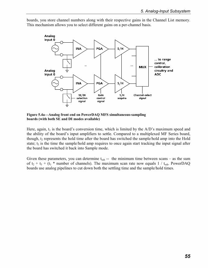
5. Analog-Input Subsystem
55
boards, you store channel numbers along with their respective gains in the Channel List memory.
This mechanism allows you to select different gains on a per-channel basis.
Figure 5.4a—Analog front end on PowerDAQ MFS simultaneous-sampling
boards (with both SE and DI modes available)
Here, again, t1 is the board’s conversion time, which is limited by the A/D’s maximum speed and
the ability of the board’s input amplifiers to settle. Compared to a multiplexed MF Series board,
though, t2 represents the hold time after the board has switched the sample/hold amp into the Hold
state; t3 is the time the sample/hold amp requires to once again start tracking the input signal after
the board has switched it back into Sample mode.
Given these parameters, you can determine tssh -- the minimum time between scans – as the sum
of t2 + t3 + (t1 * number of channels). The maximum scan rate now equals 1 / tssh. PowerDAQ
boards use analog pipelines to cut down both the settling time and the sample/hold times.
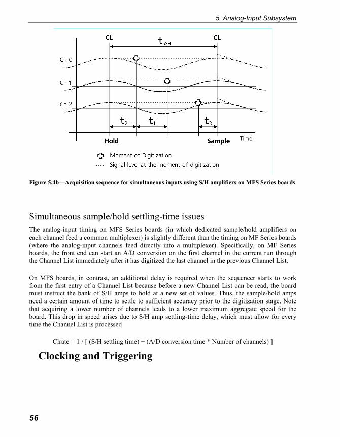
5. Analog-Input Subsystem
56
Figure 5.4b—Acquisition sequence for simultaneous inputs using S/H amplifiers on MFS Series boards
Simultaneous sample/hold settling-time issues
The analog-input timing on MFS Series boards (in which dedicated sample/hold amplifiers on
each channel feed a common multiplexer) is slightly different than the timing on MF Series boards
(where the analog-input channels feed directly into a multiplexer). Specifically, on MF Series
boards, the front end can start an A/D conversion on the first channel in the current run through
the Channel List immediately after it has digitized the last channel in the previous Channel List.
On MFS boards, in contrast, an additional delay is required when the sequencer starts to work
from the first entry of a Channel List because before a new Channel List can be read, the board
must instruct the bank of S/H amps to hold at a new set of values. Thus, the sample/hold amps
need a certain amount of time to settle to sufficient accuracy prior to the digitization stage. Note
that acquiring a lower number of channels leads to a lower maximum aggregate speed for the
board. This drop in speed arises due to S/H amp settling-time delay, which must allow for every
time the Channel List is processed
Clrate = 1 / [ (S/H settling time) + (A/D conversion time * Number of channels) ]
Clocking and Triggering
5. Analog-Input Subsystem
57
PowerDAQ cards offer considerable flexibility in how fast they digitize and collect real-world
samples. To set up any analog-input operation, you must configure both of two clocks; to activate
this operation, the subsystem must also receive a trigger pulse.
Clocking
Let’s first examine the two clocks:
• the CL clock or Channel List clock—also known as the Burst clock, it tells the control
logic when to start processing a full scan through the Channel List.
• the CV clock or Conversion clock—also known as the Pacer clock, it triggers individual
acquisitions or entries in the Channel List and thus tells the A/D how fast to digitize
successive samples.
Note When the CL clock has read the last entry in the Channel List, it automatically fetches a new set of
entries for the Channel List from the CL FIFO and sets up the mux and amplifiers to be ready to take
the next sample when a new CL clock pulse arrives.
For both of these clocks, you have the choice of four sources:
• Software clock—a software command in the application program issues a clock pulse.
• Internal clock—derived from a timebase on the board. Each PowerDAQ board offers two
software-selectable base frequencies (11 and 33 MHz). You obtain lower frequencies by
dividing the base frequency with a 24-bit divisor that has a value from 1 to 224 ( =
16,777,216). To calculate the new frequency, use the formula: Timebase = Base
Frequency / (divisor + 1). To implement this new timebase, pass the required value in the
divisor variable in the configuration function.
• External clock—the user connects this signal to a terminal panel. For instance, you might
want to export a clock from one card and have another card read that clock so both work
in a synchronized fashion. All the signals of interest on MFx Series boards are located on
the J2 digital I/O connector:
Pin 27—read external CL clock
Pin 35—export CL clock
Pin 31—read external CV clock
Pin 32—export CV clock.
Note that most of these signals are also available on J1, the main connector on the
mounting bracket that carries the analog I/O signals. However, we recommend you
working with clock signals from J2 where there is no chance that they could potentially
degrade the quality of the analog signals on which the board is operating. However, if
you are not planning to use digital I/O, using the J2 clock lines means you must purchase
an additional cable. Note further that on its external clock inputs, the board provides 4.7
kΩ pull-up resistors.
• Continuous clocking—essentially gates the clock always On, sending the next pulse at
the earliest possible opportunity.

5. Analog-Input Subsystem
58
CAUTION! If you define a clock whose speed is too high for the subsystem to
handle, the board simply ignores any pulses that arrive before it is ready to respond
to them, but it does not issue an error message.
Note Both the CL and CV clocks are required. Even if your application takes just one sample from one
channel, you must create a minimal Channel List. Failure to create this list and activate it with the CL
clock before activating the CV clock will result in false data. Put another way, a PowerDAQ card
ignores the CV clock until it senses a CL clock pulse; until you activate the Channel List, the A/D
doesn’t do any digitizing.
You define the source of each of the two clocks during the card’s configuration and initialization
stages, specifically with the command _PdAInSetCfg(). One of the parameters you pass to that
command, dwAInCfg, is a configuration word whose bits set the values of various analog-input
parameters.
More specifically, you set two configuration bits in dwAInCfg to establish the source of each clock
signal. For the Channel List clock you work with AIB_CLSTART0 and AIB_CLSTART1, and for
the Conversion clock you work with AIB_CVSTART0 and AIB_CVSTART1.
To specify a clock source, set the bits as follows (Bit 1, Bit 0)
0, 0 software clock
0, 1 internal clock
1, 0 external clock
1, 1 continuous
The default value for each of these four bits is Zero, so not setting any of the bits leaves the default
value of the two setup pairs 0,0 = software clock. To change a value there is no need to insert a
line of code that toggles the bit value; rather, merely placing its variable name in the configuration
word will change it to a One. In many situations you will want to change the values of multiple
bits to a One; you do so by ORing them. For instance, to change the CL clock to internal and the
CV clock to continuous, use AIB_CLSTART0+AIB_CVSTART0+AIB_CVSTART1, which sets
CL to 0,1 and CV to 1,1.
Note On the PDL-MF board, you can specify only one clock at a time. If you configure the CV clock as
internal or external, you must then set the CL clock to continuous. If you set the CL clock to internal
or external, the board ignores the CV clock and runs the A/D at its maximum speed.
Note The PDL-MF board provides a Gated mode when you work with the external trigger line to activate
the clock you have selected as active. If you set the bit AIB_EXTGATE by including it in the
dwAInCfg configuration word, then the board uses the ExtTrig terminal as a gate for the selected A/D
clock regardless of the clock source selected. A High on the ExtTrig terminal enables conversions,
and a Low disables them. This mode is incompatible with other trigger modes, and you should clear
all AIB_xxTRIGxx bits when working with this mode. Note also that you can implement Gated mode
on any MF/MFS boards using the 8254 counter/timers.

5. Analog-Input Subsystem
59
It’s important to realize that you can scan channels in two basic ways: either very fast by using the
CL clock to control the speed at which you start a new scan of the Channel List, or you can allow
for a specific amount of time between adjacent samples, such as to ensure that the front-end
amplifiers settle, by using the CV clock. In either case, when you set a speed on one clock, it’s
generally advisable to set the other clock to continuous mode so it has no effect on the speed of the
overall operation.
Clearly these two clocks often run at different speeds. Unless the board is sampling just one
channel, the maximum CL clock has a value of (CV clock / number of channels). As just
mentioned, setting one clock to continuous is an easy way to avoid any timing conflicts between
the two clocks. In fact, there are few cases where you might want to set both clocks exactly.
In addition, anytime you apply a clock signal before the subsystem is ready to process it, the board
generates an error condition. For example, if you input a clock at a frequency higher than the rated
aggregate rate, the board sets a bit in one of the status registers whenever a CL or CV clock pulse
occurs before it’s ready to process the pulse.
Triggering
Once you set up the Channel List clock and the Conversion clock with the commands just
described, the board doesn’t yet start collecting data. You must also supply a start trigger to
activates both clocks. The clocks are like runners at the starting line, sitting still, waiting for the
starting gun. Once the trigger signal arrives, the clocks start running. Thus, the maximum possible
delay from the time the trigger arrives to when the board digitizes its first sample is the period of
the CV clock. Similarly, you later need a stop trigger to halt both clocks. In this way, the
application has control over the exact time during which it digitizes signals. The trigger signal can
be either a software command or an external pulse, with the software trigger being the default; you
must either put a trigger command in the application or enable an external trigger.
Note If the CV clock is set to continuous or internal, the trigger is guaranteed to start and stop acquisition
at the beginning of a Channel List scan. If the CV clock is external, the external equipment is
responsible for providing enough clock pulses to complete a pass through the Channel List.
Don’t forget that if you set up the board to start on an external trigger, the analog input subsystem
ignores both the CL and CV clocks until the pulse arrives. Acquisition continues until the stop
trigger occurs. Within an application program, you generate a software trigger with the command
_PdAInSwStartTrig(). Using this command, a program can request immediate acquisition or it can
trigger an acquisition based on a review of incoming data to see if they meet some user-specified
requirement such as a certain level (see Table 5.4).

5. Analog-Input Subsystem
60
Table 5.4—External trigger modes
If you prefer to use an external clock, you apply it to Pin 29 on the J2 connector (also Pin 26 on
the J1 connector). This line, as are all logic inputs on the board, is supplied with a 4.7 kΩ pull-up
resistor. Note, though, that this pin also serves as the input for the Analog Output subsystem’s
external clock input, and obviously you can’t use that line for both purposes at the same time. The
external trigger input on a PowerDAQ board is edge-sensitive, that is, you can trigger the
acquisition to begin on either a rising or falling edge by setting the appropriate configuration bits
in the dwAInCfg word in the _PdAInSetCfg() function.
Generally, data acquisition begins immediately upon a trigger signal. In some cases, however, it’s
desirable to have analog pretriggering (examining input levels to trigger an acquisition run and
then retrieving data that led up to an external event) or analog posttriggering (starting data
collection after one of the inputs reaches a certain level). In the analog-input subsystem such
functionality must be implemented in the user application with the Advanced Circular Buffer (see
Appendix E). Note also that digital pretriggering is not possible.
Software can examine the value of incoming samples and compare them to a setpoint. Many third-
party applications include built-in functions for this task, among them are LabVIEW, DASYLab,
DIADem, TestPoint and Agilent VEE. UEI has implemented analog-trigger support in our drivers
for these packages. For example, in our LabVIEW VI named PD AIRead, that VI supplies a node
where you can activate analog triggering as well as specify parameters such as the threshold.
5. Analog-Input Subsystem
61
Clocking/Triggering Examples
A few brief examples should help you get a better idea of how to work with the clocks and
triggers.
1. Single sample
Suppose you want to take just one sample and no more. First make sure that you have defined a
Channel List, where the first entry defines the channel number and its gain setting. Next set the CL
clock to continuous, and then activate the Start trigger. Now any call to the function
_PdAInSwCvStart() generates a single pulse on the CV clock, and so it reads the next value in the
Channel List and then pauses. Because the CL clock is continuous, it effectively pulses again as
quickly as possible, once again setting the pointer to the top of that list. Thus, calling
_PdAInSwCvStart()again at any desired time digitizes just that one desired channel as before.
Recall once more that the function call will have no effect unless you have already activated the
Start trigger.
Note that you could exchange the order of the clocks; that is, you could set the CV clock to
continuous (so a reading is made immediately whenever the board activates the Channel List), and
you could use the function _PdAInSwClStart()to issue one pulse in the CL clock from an
application program. This has the same effect of reading one channel because this setup allows
one pass through the Channel List, but for this application the list contains only one entry.

5. Analog-Input Subsystem
62
2. Single scan through Channel List
As you might surmise, only a slight variation in the procedure could allow the board to make one
reading from multiple channels: simply expand the number of entries in the Channel List. In
addition, you now work with clocks a bit differently. First set the CV clock to continuous for the
fastest stepping through the list. For the CL clock, use a software source and have the application
program make a call to the _PdAInSwClStart() function to start one run though the Channel List—
assuming that you have also set the Start trigger active. Note that you need one CV clock pulse for
each entry in the Channel List, but you first need a CL clock pulse to activate the list and set the
pointer to the first entry. For instance, you can set the CV clock running free, but nothing happens
until you pulse the CL clock.
3. Multiple scans through Channel List
If you want multiple runs through the Channel List, you must pulse the CL clock each time you
want to enable another run, although the CV clock steps through the list. You might think it would
be convenient to set both clocks to continuous, but that setup is not advised because you don’t
have a reliable timebase; there might be some slight delay in starting another run and that delay
could vary from run to run.
In addition, you might think that a good option would be to set both clocks to software, but that
setup actually isn’t terribly productive. In this setup, you would theoretically call one function to
start the CL clock and then call another function to read each entry in the list; this operation would
essentially single-step through the list. If you wish to single step in this fashion, it’s far easier to
set the CL clock to continuous at the start of the program and then just use the CV clock when you
want another sample; because the CL clock is continuous, it will set the list pointer to the top of
the Channel List at the first available opportunity.
For an application that requires repeated runs through the Channel List, the recommended setup is
CL clock = internal and CV clock = continuous. The CV clock thus will step through the Channel
List as quickly as possible, and the CL clock activates the list according to the internal timebase
(either 11 or 33 MHz, modified by a user-applied divisor). Be careful when setting the timebase
because the subsystem ignores any interim clock pulses that arrive before it is able to handle them.
That situation will set an error bit but it won’t halt activity. Alternately, you could reverse the
configuration and set the CL clock = continuous and the CV clock = internal.
Table 5.5 examines all the possible clock combinations and gives you some comments on where
they are best applied. The last column tells you which bits to mention (and thereby set to One) in
the configuration word; not including the bits in this word uses the default value of Zero.
Clock combination
CL Clock
source
CV Clock
source
Typical use
Bits to set in the
dwAInCfg
configuration word
Software Continuous To acquire one set of data points (one scan). A AIB_CVSTART0+

5. Analog-Input Subsystem
63
software clock initiates one pass through the
Channel List and then the board waits for another
CL clock before restarting. This method is useful
in voltmeter type programs as well as in realtime
control and hardware-in-the-loop systems
AIB_CVSTART1
Internal Continuous For continuous acquisition with an accurate
timebase. After each CL Clock pulse, the
Channel List is executed at the maximum
acquisition rate. This is the primary mode for
use with MFS cards, and use it with MF cards
when it’s critical to minimize channel skew.
AIB_CLSTART0+
AIB_CVSTART0+
AIB_CVSTART1
External Continuous For continuous acquisition when each run of
the Channel List is triggered by an external
signal. Use this mode to synchronize scans with
external events.
AIB_CLSTART1+
AIB_CVSTART0+
AIB_CVSTART1
Continuous Continuous To perform acquisition at the maximum speed
possible. Less accurate than using the timebase.
AIB_CLSTART0+
AIB_CLSTART1+
AIB_CVSTART0+
AIB_CVSTART1
Continuous
or Software
Internal Primary mode for use with MF boards; do not
use with MFS boards. The internal CV clock
sets the time between conversions. Use this
type of clocking when you want to increase the
settling time between acquisitions, especially
when the signal source has a high output
impedance.
AIB_CLSTART0+
AIB_CLSTART1+
AIB_CVSTART0+
or
AIB_CVSTART0
Continuous External Used with MF boards only. This mode is useful
when acquiring data from just one channel, or if
you want to start a channel conversion exactly at
an external pulse edge.
AIB_CLSTART0+
AIB_CLSTART1+
AIB_CVSTART1
External or
Software
Internal Use internal CV clock on MF board to set the
time between conversions AIB_CLSTART+
AIB_CVSTART0 or
AIB_CVSTART0 External External This mode provides full control of the board’s
timing from an external device. It is rarely used
because it requires the external device it
sophisticated enough to assume all timing
functions.
AIB_CLSTART1+
AIB_CVSTART1
Software Software Although this mode gives full control of the
board’s timing to the user application, it is
rarely used because you can’t achieve high
precision compared to that possible with a
hardware clock source.
0+0 (default)
Table 5.5—Possible clocking combinations (the shaded rows at the bottom indicate rarely used
combinations).

5. Analog-Input Subsystem
64
The A/D Sample FIFO
When you collect analog samples with a PowerDAQ board, they do not go directly into host
memory. Instead, all digitized values first go into an onboard A/D FIFO memory. The standard
size of this FIFO starts at 1k samples (4k samples for high-speed 2-MHz boards), but you can
purchase options that upgrade the FIFO size to as many as 64k samples.
Note Keep in mind that a DAQ-card driver differs from one for a printer, CD-ROM or other peripheral in
one fundamental way: realtime operation. A printer can wait before it gets the next data to print; and
a CD-ROM can pause for a short while to let other activity go on. A data-acq board, however,
typically collects data continuously and can pause only as long as its onboard FIFO has sufficient
room to store intermediate results. If this buffer overflows, incoming data is lost.
This combination of an onboard DSP and a data FIFO has several advantages. First, a PowerDAQ
board can collect data at its full rated speed no matter what the host PC is doing. The DSP controls
the acquisition process and stores the data locally. So even if you’re running a graphics-intensive
application, it has no negative impact on the data-collection process. Further, virtually all of the
host CPU’s horsepower is available for post-acquisition analysis such as running a control loop.
Before moving on to other issues related to acquiring digitized data, it’s important to understand
the distinction between a scan and frame. A scan is one run through of the presently configured
Channel List. In contrast, a frame consists of a user-defined number of scans, and these datapoints
reside in a predefined portion of a buffer in host-memory. This host-memory buffer is also known
as the Advanced Circular Buffer (ACB). We elected to define these two objects to give you the
utmost in flexibility when deciding how to collect data. Keeping both scans and frames in mind,
we will now examine the various methods of moving data from the data-acq card into the host PC
where the application can use it.
Moving data into the host PC
Once you have acquired samples into the A/D FIFO buffer, you can choose from four modes that
transfer data into host memory for use by the user application.
• Normal Mode
• Fast Mode
• Bus Mastering
• Bus Mastering/Short Burst
It’s unusual that a program will use more than one of these methods. Thus, the normal procedure
is to select the desired transfer mode by going to the PowerDAQ Control Panel application,
clicking on the Driver Settings tab and selecting the mode. In the unusual event that you do want
to change transfer modes from within a user application, use the software command

5. Analog-Input Subsystem
65
_pdDiagSetPrm(). However, use this function with great caution. If not set up exactly right, the
host system could easily lock up.
1. Normal mode
In some cases, all the datapoints from an acquisition run fit easily into the A/D FIFO. In that case
you can use software commands to empty the FIFO into host memory at your convenience—but at
the latest before another acquisition run. Starting another acquisition run adds more samples to the
existing values in the FIFO. For this type of operation, you work with the first two modes, Normal
and Fast. If the FIFO is full, the board ignores any additional samples.
When you set Normal mode active, the driver transfers one-half the A/D FIFO buffer (512
samples for a 1k-sample buffer) per interrupt, but for larger buffers this transfer is never any larger
than 4k samples. While it empties one half of the FIFO, the board places newly acquired values in
the other half. The driver runs in a loop, moving a sample at a time into host memory. Further, the
driver verifies the availability of each individual sample in the before it retrieves it. Thus this is the
safest transfer mode, but it’s also the slowest. This mode works with any PCI-bus implementation.
Note The PDL-MF board does not include an onboard A/D FIFO memory. Thus, Normal mode, which
transfers data samples individually, is the only data-transfer method available for that card.
2. Fast mode
This is the default transfer mode for most MF(S) cards. Here the driver transfers samples from the
A/D FIFO into host memory using programmed I/O but without checking whether a given sample
is actually available. Thus it consumes fewer processor resources than Normal mode. As is the
case in Normal mode, the transfer size in Fast mode is the lesser of one-half the A/D FIFO or 4k
samples.
We have found that 99% of all PCI motherboards handle this mode well. However a few systems
with PCI bridges can ignore the situation that data is not yet available and nonetheless complete
the PCI Read cycle normally but with zero data. In those systems you should revert to Normal
mode.
3. Bus Mastering
In many cases, programmed I/O (Method 2) can empty the A/D FIFO in sufficient time so there is
always room in the FIFO for data coming from the next scan. However, if you collect data at a

5. Analog-Input Subsystem
66
very high rate (1 MHz or greater), the potential exists for a buffer overrun where incoming data
wants to overwrite the half of the FIFO that hasn’t yet been transferred to host memory. Such
conditions will result in an error message.
If a PowerDAQ board is configured such that the amount of incoming data could eventually
exceed the size of the FIFO buffer, you should set this mode active, whereby the DSP uses bus
mastering to handle buffer maintenance automatically. Specifically, the DSP detects when the
FIFO becomes half full and at that point initiates a data transfer from the FIFO into host memory.
This mode thus unloads the host processor from the task of transferring samples into host memory.
But because the PowerDAQ board takes control of the system bus, it might interrupt other host
processes that require bus access. Thus, you should set up the system so it doesn’t request a DMA
transfer for small amounts of data. We recommend that the minimum size of a frame for bus
mastering should be 4096 samples.
Two modes of bus-master transmissions are available, and you switch between them using the
PowerDAQ Control Panel application or the _pdDiagSetPrm() command mentioned earlier.
3a. Bus Master (standard)
Bus Master mode is employs a standard method of data transmission over the PCI bus. The board
transfers samples into locked pages of host memory that are preallocated by the VMM (virtual
memory manager). It moves data over the bus in bursts of 32 transfers, each with 32 bits of data.
Bus Master mode transfers at least 4k samples at a time regardless of the FIFO size.
Note that the PowerDAQ driver includes a special function call, _pdDiagSetPrm(), to adjust bus-
master operating parameters. However, the initial page-allocation size equals two sets of four
pages (4096 samples) and that allocation cannot be changed on the fly. Boards with larger FIFOs
can allocate more memory, as much as 16,384 samples in a single contiguous block. When the
data transfer is complete, the board fires an interrupt to the driver.
A/D FIFO Size
(k bytes)
Bus Master Transfers
when FIFO Half Full
(samples)
Bus Master
Transfers per
Interrupt
(samples)
Transfer Size in
Normal and Fast
modes (k bytes)
1 512 4096 512
2 1024 4096 1024
4 2048 4096 2048
8 4096 4096 4096
5. Analog-Input Subsystem
67
16 8192 8192 4096
32 8192 8192 4096
64 8192 8192 4096
Table 5.6—Default Bus Mastering parameters for various FIFO sizes
Our tests show that with the maximum number of boards tested simultaneously (four boards) this
mode achieves rates of 3M samples/sec per board. With a 1-GHz CPU, the load per board at this
rate is less than 5%.
3b. Bus Master/Short Burst
We developed this mode to accommodate industrial PCs with secondary bridges on the PCI bus
and that don’t properly handle PCI Abort errors and where a bus lockup can occur. In this mode,
the firmware shortens the number of 32-bit transfers per master cycle from 32 to 8, and if the
firmware encounters PCI Abort termination, it retransmits the burst completely. In this mode our
tests show transfer rates of 1.3M samples/sec per board, again with four boards running
simultaneously. The CPU load per board using this mode is <3%.
Note Some legacy PowerDAQ PD2 MF/MFS boards cannot guarantee sustained bus-mastering operation,
especially on some PCs with a secondary PCI bridge such as large industrial PCs or on machines with
a PCI-bus extender. You can identify these boards by going to the PowerDAQ Control Panel applet
(Ver 3.13 or higher) and checking which version of the Motorola DSP is on the board; a version 2
DSP indicates a board in this legacy category.
You can examine a PowerDAQ board’s data-transfer mode settings by going to the PowerDAQ
Control Panel applet. In the screen shot in Fig 5.5, the last line shows some typical settings for a
board that has a 1k-sample A/D FIFO.
xMd:1 Transfer mode—Fast mode (1)
xFh:1 Transfer size—move one 512-sample block upon FIFO half full event
xPg:8 Page size—interrupt the driver after it makes eight transfers (or 4k samples).
This value depends on the size of the FIFO installed on the board, and these
transfer parameters default to the values in Table 5.6.

5. Analog-Input Subsystem
68
Figure 5.5—Control Panel applet with typical PowerDAQ board settings
Data-transfer method tradeoffs
Depending on the speed of your board and how often you want to read new data from the board,
you must choose between programmed I/O and bus mastering. In general, if you need a short
response time, use Normal mode or Fast mode.
Consider an example of a 100-kHz board with a 1k-sample A/D FIFO. The FIFO gets emptied
when it is half full, or 512 samples / 100k samples/sec, so you have access to data every 5 msec.
In Bus Mastering you have no access to new data until incoming data can fill a full bus-master
page, which is at least 4096 samples. Thus, you would have to wait 41 msec to have access to that
data.
Another factor to consider is that under Normal and Fast modes (but not Bus Master modes) you
can take advantage of the _PdImmediateUpdate command. Among other things, it immediately
fetches all acquired samples from the board.
This command is particularly useful in these cases:
1. Acquisition rates < 10k samples/sec. If a board running at 100 Hz has the default
A/D FIFO of 1k samples, and if you select a frame size of 50 samples, you'll get 11

5. Analog-Input Subsystem
69
frames per event, a frame every 5.5 sec. To achieve better response time, include
_PdImmediateUpdate call in a timer loop.
2. When you want to clock an acquisition externally and the clock frequency can vary,
we recommend you call _PdImmediateUpdate periodically to see if any scans are
available.
3. Be aware that _PdImmediateUpdate consumes some processor time. Thus for boards
running at high acquisition rates (>100k samples/sec) we do not recommend that you
call this function more then 10 times/sec.
Host-based buffer usage
What you do with the data once they arrive in host memory can also have a major impact on
system performance. The PowerDAQ drivers set up an Advanced Circular Buffer (ACB). When
combined with applications tuned to take advantage of this flexible buffering mechanism, the
system as a whole runs much more efficiently.
Frame Markers
Buffer Tail
Buffer Head
Board/Driver
Write New Data
At Buffer Head
Application
Reads Data From
Buffer Tail
Driver AssertsFrame Done Events
When Data Written
Passes Frame
Boundry
Advanced Circular
Buffer
Figure 5.6—Advanced Circular Buffer
Once an acquisition is started, the board/driver stores data into the buffer at a known point (called
the head), while the application generally reads data at another position (known as the tail). Both
operations occur asynchronously and can run at different rates. However, you can synchronize

5. Analog-Input Subsystem
70
them by either timer notification or by a driver event. To be able to issue a notification to the user
application upon receipt of a specific sample or when incoming data reach a scan-count boundary,
the driver segments the buffer into frames. Whenever incoming data crosses a frame boundary, the
driver sends an event to the application. If multichannel acquisition is performed, the frame size
should be a multiple of the scan size to keeps pointer arithmetic from becoming unnecessarily
complex.
With the ACB, three modes of operation are possible depending on the action taken when the end
of the buffer is reached or if the buffer head catches up with the tail.
• In Single Buffer mode, acquisition stops when the driver reaches the buffer's end. The
user app can access the buffer and process data during acquisition or wait until the buffer
is full. This approach is appropriate when you're not acquiring data in a continuous
stream, and it resembles the way a digital scope operates.
• In Circular Buffer mode the head and tail each wrap to the buffer start when they reach
the end. If the head catches up to the tail pointer, the buffer is considered full and
acquisition stops. This mode is useful in applications that must acquire data with no
sample loss. Data acquisition continues until either a predefined trigger condition or the
application stops the driver. If the app can't keep up with the acquisition process and the
buffer overflows, the driver halts the acquisition and reports an error condition.
• Recycled mode resembles Circular Buffer mode except that when the head catches up
with the tail pointer, it doesn’t stop but instead overwrites the oldest scans with the new
incoming scans. As the buffer fills up, the driver is free to recycle frames, automatically
incrementing the buffer tail. This buffer-space recycling occurs irrespective of whether or
not the application reads the data. In this mode a buffer overflow never occurs. It's best
for applications that monitor acquired signals at periodic intervals. The task might require
that the system digitize signals at a high rate but not need to process every sample. Also,
an application might need only the latest block of samples.
While the ACB might seem a departure from single and double-buffer schemes you’ll see on most
other DAQ cards, it's actually a superset of them. In Single Buffer mode, the ACB behaves like a
single buffer. Configured as Circular Buffer with two frames, it behaves as a double buffer. With
multiple frames, the ACB can function in algorithms designed for buffer queues. The only
limitation, which results in more efficient performance, is that the logical buffers in the queues
can't be dynamically allocated or freed and their order is fixed.
Data format
When working with data in the host memory space, you must be aware of the format in the
datastream. Every two consecutive bytes in the stream make up one sample from the A/D
converter. These datapoints appear in a file in the order they come from the A/D converter
following the order defined in the Channel List. The format for each data word differs according
to the A/D’s resolution (PowerDAQ boards automatically place Zeros in any unused bit locations),
as shown in Fig 5.7, where bit0 is the LSB.
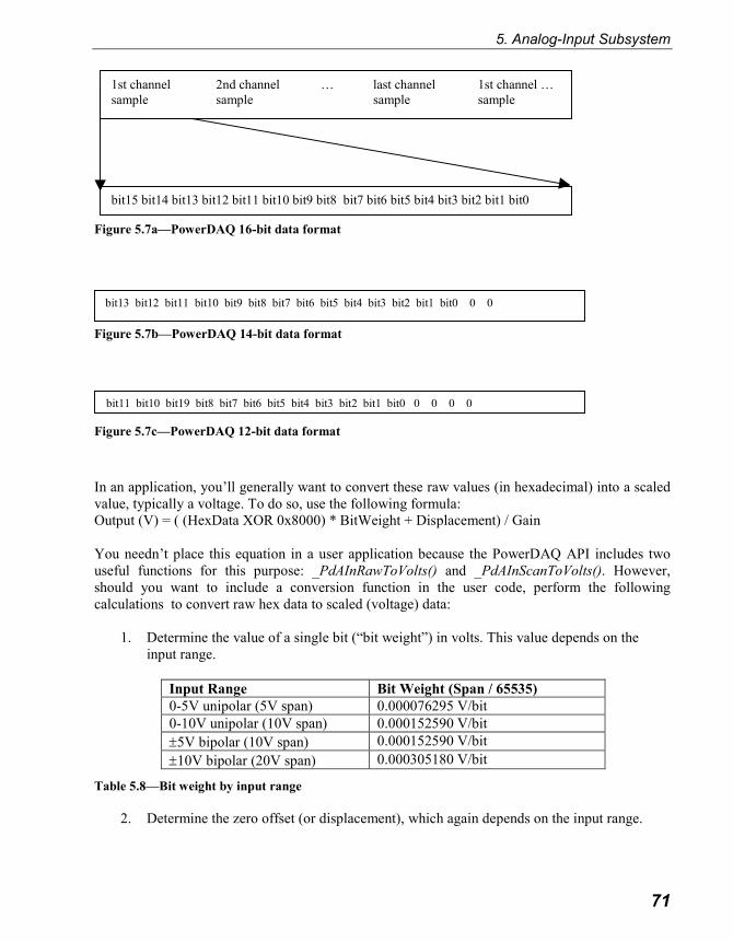
5. Analog-Input Subsystem
71
Figure 5.7a—PowerDAQ 16-bit data format
Figure 5.7b—PowerDAQ 14-bit data format
Figure 5.7c—PowerDAQ 12-bit data format
In an application, you’ll generally want to convert these raw values (in hexadecimal) into a scaled
value, typically a voltage. To do so, use the following formula:
Output (V) = ( (HexData XOR 0x8000) * BitWeight + Displacement) / Gain
You needn’t place this equation in a user application because the PowerDAQ API includes two
useful functions for this purpose: _PdAInRawToVolts() and _PdAInScanToVolts(). However,
should you want to include a conversion function in the user code, perform the following
calculations to convert raw hex data to scaled (voltage) data:
1. Determine the value of a single bit (“bit weight”) in volts. This value depends on the
input range.
Input Range Bit Weight (Span / 65535)
0-5V unipolar (5V span) 0.000076295 V/bit
0-10V unipolar (10V span) 0.000152590 V/bit
±5V bipolar (10V span) 0.000152590 V/bit
±10V bipolar (20V span) 0.000305180 V/bit
Table 5.8—Bit weight by input range
2. Determine the zero offset (or displacement), which again depends on the input range.
1st channel 2nd channel … last channel 1st channel …
sample sample sample sample
bit15 bit14 bit13 bit12 bit11 bit10 bit9 bit8 bit7 bit6 bit5 bit4 bit3 bit2 bit1 bit0
bit13 bit12 bit11 bit10 bit9 bit8 bit7 bit6 bit5 bit4 bit3 bit2 bit1 bit0 0 0
bit11 bit10 bit19 bit8 bit7 bit6 bit5 bit4 bit3 bit2 bit1 bit0 0 0 0 0

5. Analog-Input Subsystem
72
Table 5.9—Displacement by input range
3. Perform an arithmetical XOR on the raw data value with 0h8000
4. Multiply this intermediate result by the Bit Weight from Step 1
5. Add the Zero Offset from Step 2
6. If the board applied a gain other than 1 to a selected channel (as defined in the Channel
List), divide the value from Step 5 by this gain factor (this step guarantees maximal data
accuracy).
Input Range Displacement
5V or 10V unipolar 0
±5V bipolar -5V
±10V bipolar -10V

5. Analog-Input Subsystem
73
Programming Techniques
With this knowledge of the analog-input hardware, you are better prepared to understand how to
program the board to perform various digitizing functions. This subsystem is very flexible, and it
offers a variety of operating methods. Before selecting one, it’s wise to read through this manual
to understand what each does and then compare it to the application requirements.
With any of these methods, you must first specify how you are using the analog inputs, whether in
single-ended or differential mode, and indicate the range of the raw inputs prior to applying any
gain. To tell a user program which you have selected, you must OR the analog-input configuration
word dwAInCfg with one of the Mode constants in Table 5.10
Input Mode Constant for use in dwAInCfg
Single-Ended, 0-5V* 0
Single-Ended, 0-10V AIB_INPRANGE
Single-Ended, ±5V AIB_INPTYPE
Single-Ended, ±10V AIB_INPTYPE + AIB_INPRANGE
Differential, 0-5V* AIB_INPMODE
Differential, 0-10V AIB_INPMODE + AIB_INPRANGE
Differential, ±5V AIB_INPMODE + AIB_INPTYPE
Differential, ±10V AIB_INPMODE + AIB_INPTYPE + AIB_INPRANGE
* Not available in PDL-MF.
Table 5.10—Mode constants for use in analog-input configuration word
Almost every digitization task falls into one of the following categories.
• Method A—Single scan
• Method B—Burst buffered acquisition (1-shot)
• Method C—Continuous acquisition using Advanced Circular Buffer (ACB)
• Method D—Recycled-buffer mode
Method A—Single scan
A single scan, where you take one reading across the Channel List, is useful when you need to get
one set of datapoints, where a scan might even consist of just one entry in the Channel List.
Applications such as a multichannel voltmeter or sensor/thermocouple monitor are well suited for
this method. Depending on the Channel List size (maximum number of entries equals 256) and
maximum board speed, you can acquire as many as 100 scans/sec in non-realtime applications and
roughly 10 scans/sec in a realtime application.
You can initiate an acquisition with a software command or by monitoring the external CL Clock.
The maximum number of samples acquired is less then the minimal size of the A/D FIFO, so all
data stay in that FIFO and there’s no need to work with an ACB in host memory.

5. Analog-Input Subsystem
74
Note The PowerDAQ Software Suite CD-ROM contains a large number of functioning sample programs
written for various languages. They might come close to approximating what you would like an
application to do, so you might want to take a closer look at them. The examples in the SDK that fall
into the category of Method A are:
• simpleAin.c
• simplescan.pas
• simplescan.bas
• vm64.pas
• voltmeter.vbp
• Vl16.cpp
• PDGABoards.cpp
Programming Model
Now let’s take a detailed look at what’s involved when working with a program that follows the
model of Method A.
Note We urge you to read through this and all other programming models because they will give you
valuable tips on how best to work with the PowerDAQ API.
Initialization
Reset the board
PdAInReset(…)
Set up configuration
_PdAInSetCfg(…)
where dwAInCfg is the analog-input configuration word whose bits define the operating
parameters for the subsystem including the mode (SE or DI), input range, clock and trigger
sources. Analog-input configuration bits are defined in the file pdfw_def.h. Note that if you want
to change any parameter, you must make a function call that includes all the parameters, not just
the one you wish to modify. The recommended configurations for Method A are
for software clocking:
dwAInCfg = (AIB_CVSTART0 | AIB_CVSTART1)
or for an external clock
dwAInCfg = (AIB_CVSTART0 | AIB_CVSTART1 | AIB_CLSTART1)
For details on clocking options, refer back to Table 5.5.
Set up the Channel List
_PdAInSetChList(…)
where one parameter indicates the number of channels in the list, and another parameter represents
the Channel List data array.

5. Analog-Input Subsystem
75
Enable conversions
_PdAInEnableConv(…) with dwEnable = 1
_PdAInSwStartTrig(…) to issue the software-based Start trigger
Now, if you have selected the software clock, clock the first scan into the A/D FIFO.
_PdAInSwClStart(…)
Acquisition
Now the user application can instruct the board to collect analog samples as required using the
onboard timer or a program loop. In either case, you must allow sufficient time for the A/D to
acquire all points in a scan and digitize the entire Channel List. You normally allow (1 / maximum
board rate) seconds for each channel.
Note As described earlier, PowerDAQ boards have a special Slow Bit you can insert in the Channel List.
You might want to increase settling time for a particular channel when you’ve selected a high gain
setting, or for a channel connected to a signal with a high output impedance. See Appendix B for
each specific board to determine how much a Slow Bit affects the time needed to acquire a channel.
Get the samples already acquired out of the A/D FIFO and move them into the array declared in
the user application
_PdAInGetSamples(…)
If you have selected the software clock, clock in the next scan
_PdAInSwClStart(…)
Note If you are using external pulses to start clocking of the Channel List, make sure to address the
situation whereby the next scan clock comes during the _PdAInGetSamples(…) call. This function
returns the number of points stored in the buffer. If the number of scans equals the A/D FIFO size,
the subsystem could lose scan synchronization because you might not be aware of an overrun
condition. It’s possible to enable/disable conversions on the fly with _PdAInEnableConv(…), and you
can clear the A/D FIFO with _PdAInClearData(…).
Method B—Burst buffered acquisition (1-shot)
This method is useful when you need a series of 1-shot acquisitions with a significant delay
between runs. An example of such an application might be when simulating an oscilloscope or
signal analyzer, where you run an acquisition one time, stop the process, analyze the data, and run
it again as required. However, the size of the acquired data likely require buffered A/D FIFO
reads. Consequently, this method requires initializing and use of the PowerDAQ buffering
mechanism (see Appendix E).
Method B uses an asynchronous notification from the driver through Win32 events. Thus you
should program the board for asynchronous operation and use Win32 function such as
WaitForSingleObject(…) to initiate a wait until the driver notifies that the data has been
successfully acquired.

5. Analog-Input Subsystem
76
Note Examples in the SDK that fall into the category of Method B are:
• Stream2.c
• SimpleExample.vbp
Programming Model
Initialization
Reset the board
_PdAInReset(…)
Allocate and register a buffer for the board. The buffer should be accessible in both the user and
kernel spaces, and it should be locked to the physical pages. Use as big a buffer as you need; its
size is limited by the amount of memory installed on your PC. The buffer should contain at least
two frames so you can empty one while the A/D fills the other. The PowerDAQ API allocates
buffers for you.
_PdAcquireBuffer(…)
Register the buffer with the AnalogIn subsystem. Use dwMode with BUF_BUFFERWRAPPED
and BUF_BUFFERRECYCLED. for single-run operation whereby acquisition stops when the
buffer is filled.
_PdAcquireBuffer(…)
Set up the analog-input configuration and events about which you want to be notified. The analog-
input configuration bits are defined in the file pdfw_def.h. Here are the recommended
configurations for Method B:
• For the internal software clock,
dwAInCfg = (AIB_CVSTART0 | AIB_CVSTART1 | AIB_CLSTART0)
• for an external clock,
dwCfg = (AIB_CVSTART0 | AIB_CVSTART1 | AIB_CLSTART1)
Add the AIB_INTCLSBASE constant to select the 33-MHz base frequency instead of the default of
11 MHz
The application needs to know what’s going on in the buffer, so set up the board to fire events on
certain conditions. To do so, use the function
_PdSetUserEvents(…)
Analog-input event bits are defined in the file pwrdaq.h. The recommended event notification
method is
dwEvents = eFrameDone | eBufferDone | eBufferError | eStopped
Your application is notified when at least one frame is complete. Upon notification, the buffer in

5. Analog-Input Subsystem
77
host memory is filled with data or you will receive a buffer error. The most common reason for
buffer errors is heavy loading from other applications running on the PC during acquisition, so
that the system cannot service the interrupt in time. Consider using an A/D FIFO upgrades to
improve system performance (PD-16KFIFO or PD-32KFIFO) or try Method 3, bus mastering.
Initiate asynchronous operation
_PdAInAsyncInit(…)
This command sets up the data-acquisition hardware with all its basic parameters such as input
mode, type, range and clock sources. Again, you define these settings in the bits of dwAInCfg.
Provide a value for dwAInClClkDiv to set the desired scan rate. Fill and pass the Channel List as
explained in Method A. Make sure that that the aggregate rate you have set up (scan rate * number
of channels) is lower or equal to the maximum board rate.
Set up event notification
_PdAInSetPrivateEvent(…)
The API creates Win32 events and returns a valid event handle.
Acquisition
Start asynchronous operation
_PdAInAsyncStart(…)
and either have the user app issue a software trigger or wait for a hardware trigger, and then wait
for event notification that the card has digitized some data.
The following function puts your program into Sleep mode and gives the system CPU time for
other processes. The function returns control when the board signals an event or the timeout period
has expired. The timeout period should be long enough to fill your buffer with samples. When this
function returns an event from the board, you must check to see what caused it.
WaitForSingleObject(hEventObject, Timeout)
If the board is clocked from the low-frequency internal timebase or a slow external
clock, you likely won’t get an immediate event notification upon the acquisition of the
first datapoints. This is because the board transfers data from the on-board A/D FIFO
into host memory only when the FIFO reaches 50% capacity. For example, if your
board’s FIFO size is 1k samples, the acquisition rate is 100 Hz and you put only one
channel into the Channel List, the board notifies the driver (and thus the application)
only after 500 samples = 5 sec of acquisition, no matter how small your frame is. If you
clock the board externally, no response comes from the board until it gets enough
pulses to fill its FIFO half full with samples. However, you can use
_PdImmediateUpdate(…) on a timer loop to force data from the A/D FIFO into the host
buffer. Don’t call this function too often because it can degrade system performance.
Note also that this function does not work in Bus Mastering mode.
TIP

5. Analog-Input Subsystem
78
Check events with the function
_PdGetUserEvents(…)
This function returns events for the specified subsystem (here be sure to specify AnalogIn). The
user application should analyze the events and take appropriate action. An event word can contain
following flags:
• eFrameDone—a frame of data is ready for retrieval.
• eBufferDone+ eStopped—Acquisition is complete. All data is stored in the buffer and is
available for analysis.
• eBufferError—Data integrity was compromised because of a lack of performance or
system latency while serving interrupts. In such cases the on-board A/D FIFO overflows.
If this error persists, check the interrupt settings, purchase a larger A/D FIFO option or
consider using Method D with bus mastering.
Reset events. Call this function to notify the driver that events are processed.
_PdSetUserEvents(…)
Restart
The following calls stop asynchronous operation. You need to call them before you again call
_PdAInAsyncInit(…) and _PdAInAsyncStart(…). You can start and restart acquisition as many
times as the application requires. Each time you restart an acquisition, the board overwrites data in
the buffer with a new values.
_PdAInAsyncStop(…)
_PdAInAsyncTerm(…)
De-Initialization
Stop asynchronous operation
_PdAInAsyncStop(…)
_PdAInAsyncTerm(…)
Release event object handle
_PdAInClearPrivateEvent(…)
Unregister and deallocate buffer
_PdReleaseBuffer(…)

5. Analog-Input Subsystem
79
Method C—Continuous acquisition using the Advanced
Circular Buffer (ACB)
Method C employs the PowerDAQ Advanced Circular Buffer mechanism (see Appendix E). Here
you work with one part of a buffer you set up in host memory while the A/D FIFO fills the other
half. In this way, an acquisition can run continuously, and each time an event occurs (such as
frame filled), the application receives program control again. The data-acq thread waits on the
function call and won’t do anything until that call comes.
You can create separate threads for each board in your application to run the acquisition process.
Note Examples in the SDK that fall into the category of Method C are:
• Stream2.c
Set up the buffers
The analog-input configuration is very similar to Method B except you set up the buffer in a
different way. First, allocate the buffer and register it with the board. Make the buffer as large as
necessary. Here you define a frame, which is a user-defined number of scans, and you define how
many frames (and thus number of scans) must be in the buffer before the driver issues an
eFrameDone event to notify the application that data is ready for retrieval. Each user application
processes events in different ways, but each time an application detects an eFrameDone event, it
knows that one or more frames are filled with data. For Method C, the minimum buffer size is two
frames, which implements the classic double-buffering mechanism. The largest possible size is
limited by the amount of free memory in the host. A larger number of frames makes the operation
more flexible and decreases probability of buffer overflow because the host CPU isn’t involved as
frequently.
_PdAcquireBuffer(…)
When registering the buffer and if you want to use the ACB, be sure to set
Set dwWrapAround = AIB_BUFFERWRAPPED.
_PdAcquireBuffer(…)
How can you determine the optimal buffer size and number of frames? Normally four
frames in a buffer are enough to achieve smooth operation. They provide enough
time to avoid a buffer overflow if the OS encounters a delay in responding. The
buffer should be big enough to accommodate from 0.33 to 1 sec of incoming data.
TIP

5. Analog-Input Subsystem
80
How can you determine the optimal frame size for an acquisition run? When
selecting the frame size, take the following items into account. Events consume host
CPU and on-board DSP time, so a small frame needs servicing more often and thus
decreases overall system performance. On the other hand, larger frames decrease the
event rate, which isn’t desirable in situations where you need faster response,
especially in control-loop applications. We recommend setting a frame size so the
application receives from 4 to 10 events per second. For example, if the Channel List
has four entries and the acquisition rate is 100k scans/sec, the recommended frame
size is from 10,000 scans (calculated as 100k scans/10) to 25,000 scans. (calculated
as 100k scans/4).
Acquisition
Wait for event notification with
WaitForSingleObject(hEventObject, Timeout)
This function puts the user application into Sleep mode and gives the host CPU time for other
processes. The user app gets activated when the board signals an event or the timeout period has
expired. The timeout period should be long enough to fill the host buffer with samples. When this
function returns an event from the board, the application must check to see what caused it.
Check events with
_PdGetUserEvents(…)
This function returns events for the specified subsystem. The user application should analyze the
events and take appropriate action. An event word can contain following flags:
• eFrameDone—a frame of data is ready for retrieval.
• eBufferDone + eStopped—The acquisition is complete. All data is stored in the buffer
and is available for analysis.
• eBufferDone + eBufferWrapped—Incoming data has reached the end of the buffer. The
next frame that will be filled is at the start of the buffer.
• eStopped—The acquisition has stopped. The reason could be a trigger pulse on the
external trigger line, a software command or a buffer error. It’s possible that the user
application is not retrieving data from the buffer fast enough and there’s no room for new
incoming data. Check other events to find out what caused the acquisition to stop.
• eBufferError—Data integrity was compromised because of a lack of performance or
system latency while serving interrupts (see note about interrupts).
• eStopTrig—The acquisition stopped because it received the Stop trigger pulse or a
software command.
Retrieve data with
_PdAInGetBufState(…)
This function retrieves information about the position of unread frames in the buffer n scans
(ScanIndex) and the number of scans available for the application (NumValidScans). In other
words, it tells you how much new data there is and where it is located. If incoming data has passed
the buffer boundary and starts filling it from the beginning, the eFrameDone event occurs twice:
TIP

5. Analog-Input Subsystem
81
once to let the user application retrieve data at the end of the buffer (that is, from the point of the
last retrieval to the end of the buffer), and a second time to let the application retrieve data from
the beginning of the buffer to the latest complete frame. During any _PdAInGetBufState(…) call
the application gets the data in one piece. This eliminates the need for the user application to deal
with wraparound situations. Finally, note that _PdAInGetBufState(…) has a side effect: When
called, it marks frames it returns as “read” and thus these frames can be reused for new data.
Reset events with
_PdSetUserEvents(…)
Call this function to tell the driver that events have been processed.
Now perform application-specific tasks on the data. Make sure that each procedure is short enough
to process everything required before the next eFrameDone event arrives. Otherwise the buffer
can overflow and the driver can stop acquisition.
Tips for reading thermocouples and other slow-speed processes. There are two ways of
reading slow-speed processes. Method A is better when the application doesn’t require
a precise timebase and needs 10 or fewer datapoints per sec. Method C is better for rates
exceeding 10 datapoints per sec. For faster update rates, either use a
_PdImmediateUpdate(…) call on a timer loop or let the driver do the same thing by
calling _PdAInEnableTimer(…). Both functions force the board to move all samples
from the A/D FIFO to the buffer; the difference is that _PdAInEnableTimer(…) also
starts and stops the built-in timer in the driver. By making the frame sizes smaller, you
get events more quickly. Note that _PdImmediateUpdate() doesn’t work in Bus
Mastering mode.
Method D—Recycled-buffer mode
If you want to make certain that the entire buffer contains only the latest data, use the recycled-
buffer method of working with the ACB (explained in detail in Appendix E). It overwrites the
oldest frames with new data without the requirement that the data first be read. For example, you
can run an acquisition continuously as in Method C. However, if at some time the application
needs much more time to process data than the time needed to fill the frame, the acquisition
doesn’t halt and you don’t get an error message. Instead, the driver continues the acquisition and
all frames that the application hasn’t yet retrieved get overwritten with new data. When the
application receives the next event, that event sets the eFrameRecycled event flag.
One obvious situation in which to use this mode is when you cannot predict the exact time needed
to process the data. Consider the case when a control application monitors input datastreams and at
some point it needs to perform exhaustive calculations and change equipment settings. Instead of
stopping and restarting the process, Recycling buffer mode allows the data acquisition to keep
running. After processing is completed, the control application catches up with the latest data. This
mode is also suited for pretriggering applications.
TIP

5. Analog-Input Subsystem
82
Note Examples in the SDK that fall into the category of Method D are:
• Stream2.c
To switch your buffer into this mode, first call
_PdAcquireBuffer(…)
and be sure to set dwWrapAround = BUF_BUFFERRECYCLED to use the ACB’s Recycled
mode.
Combining Analog and Digital subsystems
It’s often desirable to coordinate analog inputs with digital inputs. When doing so, the part that
requires special attention is event handling. The PowerDAQ API has two sets of functions to
address this issue.
1. Set up all subsystem operations in one thread and create an event using
_PdSetPrivateEvent(…).This function creates a single event that is set when either subsystem
needs attention. Be sure to retrieve and process each active subsystem event in the order they
arrive. To release a event object, use _PdClearPrivateEvent(…).
2. Set up each subsystem operation in a separate thread. You can create a separate event object for
each subsystem using
_PdAInSetPrivateEvent(…)
_PdAOutSetPrivateEvent(…)
_PdDInSetPrivateEvent(…)
_PdUctSetPrivateEvent(…)
When one of these subsystem needs attention, it sets the appropriate event. Subsystem threads
wake up on WaitForSingleObject(…), Win32 API calls and process events as described above. To
release event objects, use the appropriate _PdxxxClearPrivateEvent(…) call.
Note Examples in the SDK that fall into the category of Method G are:
• SimpleTest.dpr
Synchronous stimulus/response
Some applications require that a test setup apply an analog stimulus to an experimental system and
then read the response read. To address this task, use a subset of Method A. Set the analog output
to generate its next datapoint on a pulse connected to that output’s external trigger line. Apply that
same pulse to one of the UCTs (user counter/timers) and have it start counting down from a
predetermined value. Upon reaching the terminal value, it generates a pulse, which you connect to
the external clock (CL Clock line) on the analog-input subsystem to start a scan. This setup
provides a user-defined delay from the analog output to the time you read the response with an
analog-input scan.

5. Analog-Input Subsystem
83
84
6. Analog-Output Subsystem
Architecture
The analog-output subsystem on every PowerDAQ multifunction board (PD2, PDL or PXI) is the
same: it consists of two 12-bit D/A converters and supports several operating methods: one single-
value update method and several waveform-generation (or streaming) methods.
The following methods are available:
Single-value update
• Method A—Single update
Buffered Waveform Generation
• Method B—Single-shot waveform generation
• Method C—Continuous waveform generation
• Method D—Repetitive waveform generation
Non-buffered Waveform Generation (backward compatibility)
• Method E—Auto-regeneration
• Method F—Events in non-buffered mode
Single-value update method
Single update (Method A)
The single update method uses an API command from the user program to write the digital
representation of the desired analog output value directly into the output register of a D/A
converter. This digital word remains in the output register indefinitely until you overwrite it with a
new value. The maximum rate at which you can update the actual analog output generated from
the D/A depends on the configuration of the host PC system, but it is at least 1 kHz.
Buffered waveform generation methods
When you are working with waveforms whose shape you know in advance, it is possible to
calculate the corresponding values for the D/A’s output register and send multiple datapoints to
the analog-output subsystem all at once. There are several ways to transfer these points:
Single-shot waveform generation (Method B)
This method outputs the waveform only once and then the subsystem stops.

6. Analog-Output Subsystem
85
Continuous waveform generation (Method C)
This method allows the continuous generation of waveforms, and there is no limit to the total
amount of data the system can output. When a frame of the buffer has been output, the driver
issues an event to allow you to write more data to the buffer.
Repetitive waveform generation (Method D)
This method can create fixed-length waveforms greater than 2048 samples. The size of the buffer
is limited by the amount of physical memory in the PC. An application writes data to the
PowerDAQ driver buffer, and each time the end of the buffer is reached, the PowerDAQ driver
resends the same buffer until instructed to stop.
Non-buffered waveform generation methods
Autoregeneration (Method E)
This method can create fixed length waveforms (maximum size limited by the D/A FIFO) without
any host PC intervention. An application writes data to the FIFO buffer, and each time the end of
buffer is reached, the DSP resends the same buffer until instructed to stop.
Note Rev 3.x of the PowerDAQ SDK allows you to create waveforms up to the size of the memory
available on your PC. (See Method D)
Events in non-buffered mode (Method F)
The events in this method allow the continuous generation of waveforms, and there is no limited
to the total amount of data the system can output. When the FIFO on the DSP drops to less than
half full, the board issues an interrupt requesting more data. Thus, with a 2k-sample FIFO, you can
load a maximum of 1024 samples at a time.
Note If the FIFO is empty and the card has sent out the last value, it continues outputting that last value
until the program instructs it to do otherwise.
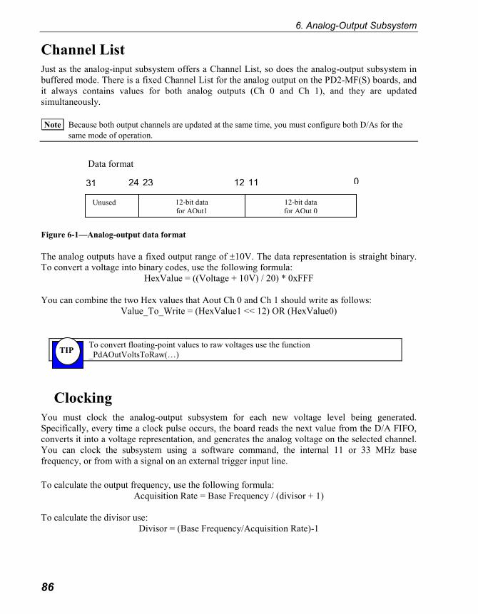
6. Analog-Output Subsystem
86
Channel List
Just as the analog-input subsystem offers a Channel List, so does the analog-output subsystem in
buffered mode. There is a fixed Channel List for the analog output on the PD2-MF(S) boards, and
it always contains values for both analog outputs (Ch 0 and Ch 1), and they are updated
simultaneously.
Note Because both output channels are updated at the same time, you must configure both D/As for the
same mode of operation.
Data format
Figure 6-1—Analog-output data format
The analog outputs have a fixed output range of ±10V. The data representation is straight binary.
To convert a voltage into binary codes, use the following formula:
HexValue = ((Voltage + 10V) / 20) * 0xFFF
You can combine the two Hex values that Aout Ch 0 and Ch 1 should write as follows:
Value_To_Write = (HexValue1 << 12) OR (HexValue0)
To convert floating-point values to raw voltages use the function
_PdAOutVoltsToRaw(…)
Clocking
You must clock the analog-output subsystem for each new voltage level being generated.
Specifically, every time a clock pulse occurs, the board reads the next value from the D/A FIFO,
converts it into a voltage representation, and generates the analog voltage on the selected channel.
You can clock the subsystem using a software command, the internal 11 or 33 MHz base
frequency, or from with a signal on an external trigger input line.
To calculate the output frequency, use the following formula:
Acquisition Rate = Base Frequency / (divisor + 1)
To calculate the divisor use:
Divisor = (Base Frequency/Acquisition Rate)-1
12-bit data
for AOut1
12-bit data
for AOut 0 Unused
0 11 12 23 24 31
TIP

6. Analog-Output Subsystem
87
Triggering
The external trigger line can serve as a Start/Stop trigger for free-running analog outputs. You can
select the internal clock as the analog-output timebase and then use the trigger line to start and
stop the output.
Additionally, the external trigger line can synchronize the analog-input and the analog-output
subsystems.
Programming Techniques
Let’s now take a look at how to program a PowerDAQ MF/MFS card’s analog-output subsystem
for each of the operating methods described above.
Method A—Single update
This simple method allows you to update the analog-output value on either or both D/As
immediately.
Note Examples in the SDK that fall into the category of Method A are:
• SimpleAOut.cpp
• SimpleTest.vbp
Initialization
Reset the board (if required)
_PdAOutReset(…)
Generate output
Output the analog output value.
_PdAOutPutValue(…)

6. Analog-Output Subsystem
88
Method B—Single-shot waveform generation
This method is useful when you need a series of single-shot waveforms with a significant delay
between runs where you output the waveform one time, stop the process, and run it again as
required. However, the size of the waveform data likely requires buffered D/A FIFO writes.
Consequently, this method requires initialization and use of the PowerDAQ buffering mechanism
(see Appendix E).
Method B uses an asynchronous notification from the driver through Win32 events. Thus you
should program the board for asynchronous operation and use Win32 function such as
WaitForSingleObject(…) to initiate a wait until the driver notifies that the data has been
successfully output.
Initialization
Reset analog output from previous operation
_PdAOutReset(…)
Acquire buffer for analog output
_PdAcquireBuffer(…) without setting the BUF_BUFFERWRAPPED flag
and fill the buffer with data
Initialize asynchronous operation
_PdAOutAsyncInit(…)
and set dwConfig = AOB_CVSTART0 to use internal clock
and calculate the divisor as described above
Set up event notification
_PdAOutSetPrivateEvent(…)
Start waveform generation
Start asynchronous operation
_PdAOutAsyncStart(…)
Wait for an eBufferDone event from the board or a timeout
WaitForSingleObject(hEventObject, Timeout)
Event handler
Check why the event object was set with
_PdGetUserEvents(…)
Re-enable events with
_PdSetUserEvents(…)

6. Analog-Output Subsystem
89
Restart
Stop asynchronous operation
_PdAOutAsyncStop(…)
_PdAOutAsyncTerm(…)
before starting again
_PdAOutAsyncInit(…)
_PdAOutAsyncStart(…)
only include
_PdAOutAsyncTerm(…)
and
_PdAOutAsyncInit(…)
if you need to change parameters
Deinitialize the subsystem
Stop asynchronous operation
_PdAOutAsyncStop(…)
_PdAOutAsyncTerm(…)
Release event object handle (optional)
_PdAOutClearPrivateEvent(…)
Release the buffer
_PdReleaseBuffer(…)
Clear the subsystem and set both outputs to 0V (optional)
_PdAOutReset(…)
Method C—Continuous waveform generation
Method C uses the PowerDAQ Advanced Circular Buffer mechanism (see Appendix E). Here you
work with one frame of a buffer you set up in host memory while the driver empties the other
frames. In this way, the output can run continuously, and each time an event occurs, the
application takes control. You can create separate threads in your application to run the acquisition
process.
Initialization
Reset analog output (if required)
_PdAOutReset(…)

6. Analog-Output Subsystem
90
Acquire buffer for analog output
_PdAcquireBuffer(…) set the BUF_BUFFERWRAPPED flag and fill the buffer with
data
Initialize asynchronous operation
_PdAOutAsyncInit(…)
and set dwConfig = AOB_CVSTART0 to use internal clock
and calculate the divisor as described above
Set up event notification
_PdAOutSetPrivateEvent(…)
Start waveform generation
Start asynchronous operation
_PdAOutAsyncStart(…)
Wait for an event from the board or a timeout
WaitForSingleObject(hEventObject, Timeout)
Event handler
Check why the event object was set with
_PdGetUserEvents(…)
Check where to put new data in the buffer
_PdAOutGetBufState(…)
and write the new data
Re-enable events with
_PdSetUserEvents(…)
Stop waveform generation
Stop asynchronous operation
_PdAOutAsyncStop(…)
_PdAOutAsyncTerm(…)
Deinitialize the subsystem
Release event object handle (optional)
_PdAOutClearPrivateEvent(…)

6. Analog-Output Subsystem
91
Release the buffer
_PdReleaseBuffer(…)
Clear the subsystem and set both outputs to 0V (optional)
_PdAOutReset(…)
Method D—Repetitive waveform generation
Use this method to create fixed-length waveforms. The PowerDAQ buffering mechanism handles
all data transfers to the D/A FIFO. After an application writes data to the buffer, the board starts to
output the waveform and restarts automatically when the pointer reaches the end of the buffer.
This method is suitable when you need a continuous repetitive waveform.
Initialization
Reset analog output (if required)
_PdAOutReset(…)
Acquire buffer for analog output
_PdAcquireBuffer(…) set BUF_BUFFERWRAPPED | BUF_BUFFERRECYCLED flags
and fill the buffer with data
Initialize asynchronous operation
_PdAOutAsyncInit(…)
and set dwConfig = AOB_CVSTART0 to use internal clock and calculate the divisor as described
above
Set up event notification
_PdAOutSetPrivateEvent(…)
Start waveform generation
Start asynchronous operation
_PdAOutAsyncStart(…)
Wait for an event from the board or a timeout
WaitForSingleObject(hEventObject, Timeout)
Event handler
Check why the event object was set with
_PdGetUserEvents(…)
6. Analog-Output Subsystem
92
Re-enable events with
_PdSetUserEvents(…)
Stop waveform generation
Stop asynchronous operation
_PdAOutAsyncStop(…)
_PdAOutAsyncTerm(…)
Deinitialize the subsystem
Release event object handle (optional)
_PdAOutClearPrivateEvent(…)
Release the buffer
_PdReleaseBuffer(…)
Clear the subsystem and set both outputs to 0V (optional)
_PdAOutReset(…)
Method E—Autoregeneration
Use this method to create fixed-length waveforms (2048 samples maximum, or 65536 with
external memory) without using any host CPU cycles; the onboard DSP handles all subsystem
operations. It’s easier than using Method D, but the size is limited to the D/A FIFO size. After an
application writes data to the D/A FIFO, the board starts to output the waveform and the
subsystem restarts automatically when the pointer reaches the end of the buffer. This method is
suitable when you need a continuous repetitive waveform less than or equal to the D/A FIFO size.
Note Examples in the SDK that fall into the category of Method E are:
• SimpleTest.dpr
Initialization
Reset the analog output (optional)
_PdAOutReset(…)
Set the analog-output configuration
_PdAOutSetCfg(…)

6. Analog-Output Subsystem
93
setting dwConfig = AOB_CVSTART0 | AOB_DACBLK0 | AOB_DACBLK1 | AOB_REGENERATE
to use the 11-MHz internal clock for autoretriggerable waveform generation.
Set the timebase
_PdAOutSetCvClk(…)
using the same calculations to set up the timebase as described in the analog-input subsystem
Write data to the D/A FIFO with
_PdAOutPutBlock(…)
Start waveform generation
_PdAOutEnableConv(…) using 1 as the value for dwEnable
_PdAOutSwStartTrig(…)
Stop waveform generation
Reset the analog-output subsystem (optional)
_PDAOutReset(…)
Note The board also stops waveform generation when it reaches the end of the buffer.
Method F—Event-based waveforms using PCI
interrupts
There are several ways to generate long continuously changing waveforms. The event-based
waveform technique empties the board’s onboard FIFO memory into the analog-output subsystem.
When the FIFO is less than half full, the board sends an interrupt to the host to request additional
data. You can process analog-output events in a separate event handler or in the common event
handler for all subsystems. Please note that Method C has replaced Method F, which we include
for backward compatibility.
Note Examples in the SDK that fall into the category of Method F are:
• AOEvents.c
• AEOutBlk.vbp

6. Analog-Output Subsystem
94
Initialization
Reset the analog output
_PdAOutReset(…)
This function resets both analog outputs to 0V, and you must reset all operating parameters before
running an analog output.
Set the analog-output configuration with
_PdAOutSetCfg(…)
and set dwConfig = AOB_CVSTART0 to use the 11-MHz internal base clock.
Set the timebase with
_PdAOutSetCvClk(…)
and use the same calculations to set up the timebase as described in the analog-input subsystem.
Set up an event object
_PdAOutSetPrivateEvent(…)
Enable the interrupt
_PdAdapterEnableInterrupt(…)
Set the events about which you wish to be notified
_PdSetUserEvents(…)
and set dwEventsNotify = eFrameDone | eBufferDone | eBufferError | eStopped. You need these
all for event-based waveform mode. Don’t forget to set the subsystem parameter to AnalogOut
Write the first block of data
_PdAOutPutBlock(…)
Enable and start analog-waveform generation
_PdAOutEnableConv(…) using 1 for dwEnable
_PdAOutSwStartTrig(…)
Note To start waveform generation with a software command, use _PdAOutSwStartTrig(). If you wish to
synchronize an analog output with an external trigger, set the appropriate flags in _PdAOutSetCfg().
Note that the flags AOB_STARTTRIG0, AOB_STARTTRIG1, AOB_STOPTRIG0 and
AOB_STOPTRIG1 have the same functionality as for the analog-input subsystem.
Wait for events and process them using the Win32 API call
WaitForSingleObject(…).
Event handler
Check why the event object was set with
_PdGetUserEvents(…)

6. Analog-Output Subsystem
95
Examine the return from this function for these events: eFrameDone means that the D/A has
output a voltage for half the values in the D/A FIFO; eBufferDone + eBufferError means that the
D/A has emptied the entire buffer and that no more datapoints are available.
Re-enable events with
_PdSetUserEvents(…)
Write additional data to the D/A FIFO with
_PdAOutPutBlock(…)
Continue waveform generation
_PdAOutEnableConv(…) and use 1 for dwEnable
_PdAOutSwStartTrig(…)
Stop waveform generation
Issue a stop trigger if you haven’t configured the external trigger
_PdAOutSwStopTrig()
and then disable D/A conversions
_PdAOutEnableConv(…) and use 0 (FALSE) for dwEnable
De-initialize the subsystem
Disable the board interrupt (if no other subsystem are using the interrupt at the time)
_PdAdapterEnableInterrupt(…) and use dwEnable = 0
Release the event object
_PdAOutClearPrivateEvent(…)
Clear the subsystem and set both outputs to 0V.
_PdAOutReset(…)

96
7. Digital I/O Subsystem
Architecture
The digital I/O subsystem in almost all PD2/PDXI MF/MFS Series boards contains one 16-bit
input register and one 16-bit output register. The only exception is the PDL-MF, which uses two
24-bit registers. In all cases, the digital I/O registers do not support clocked operation, so this
subsystem can be used only in software-polled mode.
Figure 7.1—Digital-input subsystem hardware block diagram
On all dedicated digital input lines the board comes with 4.7kΩ pull-up resistors. (We supply these
pull-up resistors on all digital inputs including all external trigger lines, all external clock inputs
and counter/timer inputs.)
In the standard configuration (excluding the PDL-MF), the eight lower lines of the digital input
connect to a latch register. You can then program this register to detect rising or falling edges on
these lines.

7. Digital I/O Subsystem
97
To configure the latch you send a 16-bit word, two bits being assigned to each of the eight sense
inputs. Setting the F bit for a given input to a One makes that input sensitive to a falling edge;
setting the R bit to a One makes that input sensitive to a rising edge.
Bit 7 Bit 6 Bit 5 Bit 4 Bit 3 Bit 2 Bit 1 Bit 0
F R F R F R F R F R F R F R F R
Figure 7.2—Digital-input configuration word
The latch register in the digital-input subsystem provides one status bit for each line. When it
detects the configured edge (falling or rising), the detection/latch logic does two things. First, it
sets this status bit to a One; second, it fires an interrupt to inform the DSP that the configured
conditions have been met.
If you set up a latch to watch for edges on several lines, the interrupt fires as soon as any of the
selected conditions happens. However, the interrupt will not refire until the user application clears
the status bit for that first line. Then, when the logic detects another change on any line, the
interrupt fires again. To determine which line has caused an interrupt, the user program must read
the digital-input status bits in the latch register.
Programming Techniques
The digital input/output subsystem can be used in two ways, and recall that this subsystem has no
clocked operations available.
Method A—Polled I/O
This method works by using software to poll 16 digital inputs and 16 digital outputs.
Note Examples in the SDK that fall into the category of Method A are:
• SimpleTest.dpr
Initialization
Reset the digital subsystem
_PdDOutReset(…) sets the output lines to Zero
_PdDInReset(…)clears the latch and the configuration register

7. Digital I/O Subsystem
98
Set up the digital input configuration
Set up edge-sensitivity configuration with
_PdDInSetCfg(…)
Specify an input line and an edge to be detected using a configuration word as described earlier in
this section.
Read the status of the digital input latch with
_PdDInGetStatus(…)
This function returns the current state of the digital-input lines in one byte and the status of the
digital-input latch register in a second byte. If the specified edge was detected, the latch contains a
One in the appropriate bit.
Clear the status of the digital input latch with
_PdDInClearData(…)
This function clears the latch register and re-enables edge detection on the line that previously
caused an event
Input/output
Read digital inputs
_PdDInRead(…)
Write digital outputs
_PdDOutWrite(…)
It’s possible to acquiring a digital signal using analog techniques. as analog. In an
application where you need to acquire some digital signals along with an analog input,
you can build a simple D/A converter using a resistor ladder. It allows you to convert up
to eight digital input lines into one analog signal, which you then digitize and from its
value you can determine the values of the original digital bits. for reliable detection using
a 12-bit PowerDAQ board.
TIP

7. Digital I/O Subsystem
99
Method B—Generate an event upon edge detection
In this scheme you set up an input configuration, and the subsystem fires an event when it detects
a specified edge on the corresponding input line. The eight lower lines of the 16-bit digital input
subsystem are edge-sensitive.
The setup parameters for this method are very similar to those used in Method A. The difference is
that you should additionally enable and set up event notification. As does the analog-output
subsystem, digital inputs can share an event handler with other subsystems or have a dedicated
event handler.
Note Examples in the SDK that fall into the category of Method B are:
• DIEvents.c
Initialization
Reset the digital-input subsystem with
_PdDInReset(…)
to clear the latch and configuration register
Set up the digital-input configuration
Set up the edge-sensitivity configuration
_PdDInSetCfg(…)
Specify an input line and an edge to be detected using a configuration word as described earlier in
this section.
_PdAdapterEnableInterrupt(…) with dwEnable set to 1
_PdDInSetPrivateEvent(…) sets up event object
_PdSetUserEvent(…)
and use DigitalIn as a subsystem name. The driver defines only one digital-input event,
eDInEvent, which means that one or more edges were detected
Event handler
Check event
_PdGetUserEvent(…)
should return the eDInEvent flag in the status word.
Read the status of the digital-input latch
_PdDInGetStatus(…)
7. Digital I/O Subsystem
100
This function returns the current state of the digital-input lines in one byte and the status of the
digital-input latch register in a second byte. If the specified edge was detected, the latch contains a
One in the appropriate bit.
Clear the status of the digital input latch with
_PdDInClearData(…)
It clears the latch register and re-enables edge detection on the line that previously caused an event
Re-enable events with
_PdSetUserEvent(…)
and use DigitalIn as a subsystem name. The driver defines only one digital-input event,
eDInEvent, which means that one or more edges were detected
De-Initialization
Disable interrupts if there is no other subsystem running
_PdAdapterEnableInterrupt(…) with dwEnable set to 0
Release the event object and clear user-level events
_PdDInClearPrivateEvent(…)
_PdClearUserEvent(…) and use DigitalIn as the subsystem name
Reset the digital inputs to clear the configuration and latch registers
_PdDInReset(…)

7. Digital I/O Subsystem
101
102
8. User Counter/Timer Subsystem
Architecture
Unlike the counter/timers on many other data-acq boards, those on the MF/MFS Series boards are
fully dedicated to user tasks. You can set up the three on-board counter-timers to any mode
compatible with the Intel 82C54 chip. Using a counter/timer output to control the analog-input and
-output subsystems can result in setups that perform sophisticated data-acquisition tasks. Certain
applications, though, might require you to build external digital circuitry.
Additionally, when they reach Zero counts these counter-timers can generate events, which can
clock other subsystems and perform various operations.
The user counter/timer (UCT) subsystem on MF/MFS Series boards is based on Intel’s 16-bit
82C54 counter-timer chip (again, the PDL-MF has a different configuration as described below).
That device contains three counter/timers that are not required by any PowerDAQ subsystems and
thus are fully dedicated to user applications. Further, the three counter/timers are fully independent
so that each can function in a different mode, if desirable.
Note: You can combine UCT0 with UCT1 to implement a 32-bit counter or use UCT0 as a
common prescaler for UCT1 and UCT2.
The 82C54 solves a common problem that arises in setting up test systems, the generation of
accurate time delays under software control. Instead of setting up timing loops in software, the
programmer configures the chip to meet system requirements and programs one of the counters for
the desired delay. After the desired delay, the 82C54 interrupts the CPU. Software overhead is
minimal and variable-length delays can easily be accommodated.
Some other counter/timer functions you can easily implement with the 82C54 are:
• Event counter
• Digital one-shot
• Programmable rate generator
• Squarewave generator
• Binary rate multiplier
• Complex waveform generator
• Complex motor controller
The UCT is extremely useful in combination with the external clock and trigger lines. Using the
UCT you can create very sophisticated acquisition setups.

8. User Counter/Timer Subsystem
103
At a high level, the programmer need only be concerned with selecting the input clock source and
then selecting the gate signal (setting the Gate to Logic 1 enables counting; setting it to Logic 0
disables counting; it has no effect on the counter/timer output lines). The UCT generates an output
signal depending on its operating mode and the input conditions. In addition, a counter/timer’s
outputs can also generate an interrupt to the host PC when a change in state occurs.
You can feed a clock input from one of the following sources:
• Software command
• 1-MHz internal timebase
• External clock input line (10 MHz max)
• Output from UCT0 (available as input for UCT1 and 2)
It is possible to control the gate from the following sources:
• Software command
• External gate input line
You can operate each UCT in several modes (for details, see the 82C54 datasheet available on the
Intel web site):
• Single pulse (82C54 Mode 1)—The output line is initially High, and it goes Low on the
clock pulse following a trigger on the gate line to begin a 1-shot pulse. It remains Low
until the counter reaches zero. At that point the output again goes High and remains in
that state until the clock pulse after the next trigger.
• Pulse train (82C54 Mode 2)—This mode functions like a divide-by-N counter so the
pulse length equals 1 / clock frequency. The output line is initially High. When the initial
count decrements to 1, the output goes Low for one clock pulse, and then it goes High
again at which time the counter reloads the initial count and the process repeats. This
mode is periodic, and the same sequence repeats indefinitely until it is instructed to stop.
• Rate (82C54 Mode 3)—This mode is similar to Pulse train mode except for the output
line’s duty cycle. That line is initially High, and when half the initial count has expired it
goes Low for the remainder of the count. The sequence repeats indefinitely. An initial
count of N results in a square wave with a period of N clock cycles.
• Delay (82C54 Mode 5)—This mode generates a single pulse after waiting a programmed
amount of time. The output line is initially High. The rising edge of the gate line triggers
counting. When the initial count has expired, the output line goes Low for one clock
pulse and then returns to a High state.
A special frequency measurement mode is implemented on PD2/PDXI boards. Using this mode
you can measure an external frequency; you connect the signal to the counter’s input terminal and
measure the number of counts (up to 65,535) that arrive in a 1-sec interval (see the
UCTMeasFrequency example program).
Note It’s not necessary to implement an event handler and enable interrupts for most UCT applications. Set
one up only if the application must be informed on specific countdown conditions.

8. User Counter/Timer Subsystem
104
Note You can use UCT to stop an analog acquisition run after acquiring N scans. To do so, program the
device to count the N scans, and also connect its output to the analog input’s external trigger. Then
set up the A/D to stop on the external trigger’s falling edge of the external trigger.
PDL-MF-X
The PDL-MF also supplies three user counter/timers, but they are implemented with 24-bit
registers on the 56301 DSP. They are independent of each other and can generate interrupts. The
maximum clock frequency is 16.5 MHz for an external clock and 33 MHz for an internal clock.
Please refer to Motorola DSP56301 user manual for details.
This UCT functions in the following modes:
• timer
• external event counting
• pulse output
• squarewave output
• PWM (pulse-width modulation) output
• width/period/capture measurement
Note On the MF-PDL card, TMR0 is shared with the AIn clock; TMR2 is shared with the AOut clock.

8. User Counter/Timer Subsystem
105
Programming Techniques
Programming the Intel 82C54 can be difficult because of its various modes and settings. To ease
this job, the PowerDAQ SDK provided the definitions you need along with a set of example
functions in the file uct_progr.c, which is located in the same folder with the UCTEvents Visual
C++ example. Please refer to that file and to the Intel 82C54 datasheet to assist you in learning
how to program the UCT subsystem.
Please be aware that the PowerDAQ API provides separate event flags for each
counter/timer.
Note To write to the counter/timer, you must apply an input clock to the selected UCT. You can control its
Gate line using the _PdUctSwSetGate(…) function.
Note Examples in the SDK that fall into the UCT category are:
• DIEvents.c
• uct_progr.c
• SimpleTest.dpr
• SimpleTest.vbp
Using UCT events
Initialization
Reset the UCT subsystem with
_PdUctReset(…) to clear the latch and configuration register
Set up UCT configuration
Set up the edge-sensitivity configuration
_PdUctSetCfg(…)
and refer to uct_progr.c in the SDK files for bit definitions
_PdAdapterEnableInterrupt(…) using dwEnable = 1
_PdUctSetPrivateEvent(…) sets up event object
_PdSetUserEvent(…)
and use CounterTimer as the subsystem name. The driver defines three events, one for each
counter/timer: eUct0Event, eUct1Event and eUct2Event
8. User Counter/Timer Subsystem
106
Event handler
Check for an event
_PdGetUserEvent(…)
can return either the eUct0Event, eUct1Event or eUct2Event flag in the status word.
Read the status of the UCT output
_PdUctGetStatus(…)
Re-enable events
_PdSetUserEvent(…)
Deinitialization
Disable interrupts if no other subsystem is running
_PdAdapterEnableInterrupt(…) while setting dwEnable = 0
Release the event object and clear user-level events
_PdUctClearPrivateEvent(…)
_PdClearUserEvent(…) using CounterTimer as the subsystem name
Reset the UCT to clear its configuration and stop ongoing operations
_PdUctReset(…)

8. User Counter/Timer Subsystem
107
108
9. Support Software
PowerDAQ Example Programs
A complete range of sample programs with source code is included with each PowerDAQ board
as part of the PowerDAQ Software Suite CD-ROM. For complete details on programming the
PowerDAQ board, refer to the PowerDAQ Software Manual
Note Listed below are summaries of just a few of the examples we supply. Please review the installation
directories for new examples or visit us online at www.PowerDAQ.com
Visual C++ examples
Versions supported: VC 1.5 (16 bit), VC 5 and 6 (32 bit)
Examples supplied:
• VM16.exe–simple voltmeter application displaying as many as 64 channels.
• Stream4.exe–continuous acquisition and stream-to-disk application.
Visual BASIC examples
Versions supported: VB 3 (16 bit), VB 5 and 6 (32 bit)
Examples supplied:
• The SimpleTest utility (SimpleTest.vbp), which allows the simultaneous operation, if
desired, of all subsystems: Analog Input, Analog Output, Digital Input, Digital Output
and Counter/Timer operation.
• Additional examples are located on the PowerDAQ Software Suite CD-ROM in the
VBExecutables directory. After running the installation, look in the
PowerDAQ\SDK\Examples\VisualBasic\VB5 (OR VB6)\[Example Name] directory.
Delphi examples
Versions supported: Delphi 3 and 4 (32-bit)
9. Support Software
109
Examples supplied include the following:
• The SimpleTest utility (SimpleTest.dpr), which allows the simultaneous operation, if
desired, of all subsystems: Analog Input, Analog Output, Digital Input, Digital Output
and Counter/Timer operation.
Borland C++ Builder examples
Versions supported: Inprise/Borland 3.5
Examples supplied:
• Stream4.exe – continuous acquisition and stream-to-disk application.
Note The files included for the above programming languages may have the same file name. This means
they can be used with either language.

9. Support Software
110
Third-Party Software Support
The PowerDAQ CD contains drivers for most popular third-party software packages. The
installation procedure automatically detects if you have installed any of the third-party packages,
and will install the drivers and examples automatically. If you install a third-party software
package after installing the PowerDAQ software, you must reinstall our software to include
support for this new third-party package.
As of the writing of this manual, we support the following third-party software:
Software
Package
Version Supports
multiple
PowerDAQ
boards
What’s included
LabVIEW 5.x or greater Yes Extensive VIs including click-
and-replace low-level VIs
LabVIEW for Linux 6.x or greater Yes VIs that mirror standard
LabVIEW support but run under
Linux
LabVIEW Real-
Time
6.x or greater Yes VIs that mirror standard
LabVIEW support but run under
this environment.
Agilent VEE 5.x or greater Yes Examples
DASYLab 4.x or greater No Examples
TestPoint 3.3 or greater Yes Examples
LabWindows/CVI 5.x or greater Yes Callable from our VC++ support
DIADEM 6.x or greater Yes Examples
MATLAB Data-
Acquisition
Toolbox
6.x or greater Yes Examples
xPC Target 2.x or greater Yes Examples
Table 9.1—Third-party software support

9. Support Software
111

112
Appendix A: Specifications

Appendix A: Specifications
113
PD2-MF Multifunction Boards
Model: PD2-MF-xx- 3M/12x 2M/14H 1M/12x 500/16x
Resolution 12 bits 14 bits 12 bits 16 bits
Number of Channels
Single-Ended
Differential
16 or 64
8 or 32
Maximum Sampling Rate 3M S/sec 2.2M S/sec 1.25M S/sec 500k S/sec
Onboard FIFO Size
(upgradeable to 16k, 32k, 64k)
16k samples 4k samples 2k samples
Channel-Gain List 256 entries
Input Ranges 0–5V, 0–10V, ±5V, ±10V
(software selectable)
Programmable Gains
by channel
L=1,10,100,1000
H=1, 2, 4, 8
H=1, 2, 4, 8
L=1,10,100,1000
H=1, 2, 4, 8
Drift
Zero
Gain
±30 µV/°C
±30 ppm/°C
Input Impedance 10 MΩ
Input Bias Current ±20 nA
Input Overvoltage ±20V,2000V ESD
10 mA max
±35V continuous
A/D Conversion Time 283 ns 0.45 µsec 0.8 µsec 2 µsec
A/D Settling Time 250 ns 0.37 µsec 0.6 µsec 1.2 µsec
DC Accuracy
Nonlinearity ±1 LSB ±2 LSB ±0.5 LSB ±1 LSB
System Noise 0.8 LSB 1.2 LSB 0.3 LSB 1.3 LSB
AC Accuracy
Effective Number of Bits 11.2 12.2 11.63 14.5
Total Harmonic Distortion+
Nonlinearity+Noise
72 dB 76 dB 71.8 dB 88 dB
Channel Crosstalk -80 dB @ 1k S/sec
Clocking and Trigger Input
Maximum A/D Pacer Clock
Aggregate Throughput
@ 0.01% Accuracy
3000k S/sec
2200k S/sec @ 1 ch
1800k S/sec @ all
1250k S/sec
500k S/sec
External A/D Sample Clock
Maximum Frequency
3000k S/sec
2200k S/sec @ 1 ch
1800k S/sec @ all
1250k S/sec
500k S/sec
Minimum Pulse Width 20 nsec
External Digital (TTL)Trigger
High-level Input Voltage
Low-level Input Voltage
Minimum Pulse Width
2.0V min
0.8V min
20 nsec

Appendix A: Specifications
114
Model: PD2-MF-xx- 400/14x 333/16x 150/16x
Resolution 14 bits 16 bits 16 bits
Number of Channels
Single-Ended
Differential
16 or 64
8 or 32
16
8
Maximum Sampling Rate 400k S/sec 333k S/sec 150k S/sec
Onboard FIFO Size
(upgradeable to 16k, 32k, 64k)
1k samples
Channel-Gain List 256 entries
Input Ranges 0–5V, 0–10V, ±5V, ±10V (software selectable)
Programmable Gains
by channel
L = 1,10,100,1000
H = 1, 2, 4, 8
Drift
Zero
Gain
±30 µV/°C
±30 ppm/°C
Input Impedance 10 MΩ
Input Bias Current ±20 nA
Input Overvoltage ±35V continuous
A/D Conversion Time 2.5 µsec 2.0 µsec 6 µsec
A/D Settling Time 2.0 µsec 1.2 µsec 5 µsec
DC Accuracy
Nonlinearity ±0.5 LSB ±1 LSB ±1 LSB
System Noise 0.8 LSB 1.3 LSB 1.2 LSB
AC Accuracy
Effective Number of Bits 13.1 14.5 14.8
Total Harmonic Distortion+
Nonlinearity+Noise
81 dB 89 dB 91 dB
Channel Crosstalk -80 dB @ 1k S/sec
Clocking and Trigger Input
Maximum A/D Pacer Clock
Aggregate Throughput
@ 0.01% Accuracy
400k S/sec
333k S/sec
150k S/sec
External A/D Sample Clock
Maximum Frequency
400k S/sec
333k S/sec
150k S/sec
Minimum Pulse Width 20 ns
External Digital (TTL)Trigger
High-level Input Voltage
Low-level Input Voltage
Minimum Pulse Width
2.0V min
0.8V min
20 nsec

Appendix A: Specifications
115
Analog Outputs - all PD2-MF models
Number of Channels 2
Resolution 12 bits
Update Rate 200k S/sec each
Onboard FIFO Size 2k samples (on DSP)
Analog Output Range ±10V
Error
Gain ±1 LSB
Zero Calibrated to 0
Current Output ±20 mA max
Output Impedance 0.3Ω typ
Capacitive Drive Capability 1000 pF
Nonlinearity ±1 LSB
Protection Short circuit to analog ground
Power-on Voltage 0V ±10 mV
Setting Time to 0.01% of FSR 10 µsec, 20V step
1 µsec, 100-mV step
Slew Rate 30 V/µsec
Counter/Timer - all PD2-MF models
Number of Counters 3 available to user
(Intel 82C54)
Resolution 16 bits on each counter
Clock Inputs:
Software configurable
High-level Input voltage
Low-level Input voltage
High-level Input current
Low-level Input current
Internal 1M S/sec
External < 10M S/sec
2.0V min
0.8V max
20 µA
-20 µA
Gate Inputs:
Maximum Pulse Width
100 nsec (High) 100 nsec (Low)
Counter Outputs:
Output Driver High Voltage
Output Driver Low Voltage
Inverted
2.5V min (IOH = 24 mA)
0.55V max (IOH = 48 mA)

Appendix A: Specifications
116
Digital I/O—all PD2-MF models
Input Bits
(8 can generate IRQ)
16
Output Bits 16
Inputs:
High-level Input Voltage
Low-level Input Voltage
High-level Input Current
Low-level Input Current
2.0V min
0.8V max
20 µA
-20 µA
Outputs:
Output Driver High Voltage
Output Driver Low Voltage
2.5V min, 3.0V typ (IOH = -32 mA)
0.55V max (IOL = 64 mA)
Current Sink -32/64 mA max, 250 mA per port
Pulse Width 20 ns min, interrupt bit latched on rising,
falling or either edge
Power-on Voltage Logic Zero
General Specifications and Connectors - all PD2-MF models
Power Requirements 5V
Physical Dimensions 10.5 x 3.8” (262 x 98 mm)
Environmental:
Operating Temperature Range
Storage Temperature Range
Relative Humidity
0 to 70°C
-25 to 85°C
to 95%, noncondensing
Connector J1 96-pin high-density Fujitsu connector (male)
(Fujitsu PN#FCN-245P096-G/U)
Connector J2 36-pin header connector (male)
(Thomas and Betts PN#609-3627)
Connector J4 36-pin header connector (male)
(Thomas and Betts PN#609-3627)
Connector J6 8-pin male connector
(Adam-Tech PN#PH2-SMT-8-SGA)

Appendix A: Specifications
117
PD2-MFS Simultaneous Sampling Boards
Model: PD2-MFS-xx- 2M/14 1M/12 800/14
Resolution 14 bits 12 bits 14 bits
Number of Channels
Single-Ended
Differential
4 (8 optional)
4 (8 optional)
Maximum Sampling Rate
(multiple channels)
2M S/sec 1M S/sec 800k S/sec
Onboard FIFO Size (upgradeable
to 16k, 32k, 64k)
4k samples 1k samples
Input Ranges 0–5V, ±5V,
0–8V, ±8V @ 10V
ranges
0–5V, 0–10V, ±5V, ±10V
(software selectable)
Channel-Gain List 256 entries
Programmable Gains
by channel
256 entries
Drift
Zero
Gain
±30 µV/°C
±30 ppm/°C
Input Impedance 1 MΩ
Input Bias Current ±100 pA
Input Overvoltage
A/D Conversion Time 0.45 µsec 0.8 µsec 1.25 µsec
SSH Amp Settling Time 0.7 µsec 0.9 µsec 1.0 µsec
A/D Settling Time 0.4 µsec 0.6 µsec 1.25 µsec
DC Accuracy
Nonlinearity
(no missing codes)
±2 LSB ±0.5 LSB ±0.5 LSB
AC Accuracy
Effective Number of Bits 12.1 11.3 12.7
Channel Crosstalk -80 dB @ 1k S/sec
Clocking and Trigger Input
Maximum A/D Pacer Clock 1500k S/sec, 4 ch,
1700k S/sec, 8 ch
975k S/sec, 4 ch,
1095k S/sec, 8 ch
800k S/sec
External A/D Sample Clock
Maximum Frequency
1500k S/sec, 4 ch
1700k S/sec, 8 ch
975k S/sec, 4 ch,
1095k S/sec, 8 ch
800k S/sec
Minimum Pulse Width 20 nsec
External Digital (TTL)Trigger
High-level Input Voltage
Low-level Input Voltage
Minimum Pulse Width
2.0V min
0.8V min
20 nsec

Appendix A: Specifications
118
Model: PD2-MFS-xx- 500/16 500/14 300/16
Resolution 16 bits 14 bits 16 bits
Number of Channels
Single-Ended
Differential
4 (8 optional)
4 (8 optional)
Maximum Sampling Rate
(multiple channels)
500k S/sec 500k S/sec 300k S/sec
Onboard FIFO Size (upgradeable to
16k, 32k, 64k)
1k samples
Input Ranges 0–5V, 0–10V, ±5V, ±10V (software selectable)
Channel-Gain List 256 entries
Programmable Gains by channel 1, 2, 5, 10
Drift
Zero
Gain
±30 µV/°C
±30 ppm/°C
Input Impedance 1 MΩ
Input Bias Current ±100 pA
Input Overvoltage ±18V SE, ±40V DI
A/D Conversion Time 2 µsec 2.0 µsec 3 µsec
SSH Amp Settling Time 1.2 µsec 1.2 µsec 1.2 µsec
A/D Settling Time 1.5 µsec 1.2 µsec 2.7 µsec
DC Accuracy
Nonlinearity
(no missing codes)
±1 LSB ±1 LSB ±1 LSB
AC Accuracy
Effective Number of Bits 13.8 12.7 13.8
Channel Crosstalk -80 dB @ 1k S/sec
Clocking and Trigger Input
Maximum A/D Pacer Clock 500k S/sec 300k S/sec
External A/D Sample Clock
Maximum Frequency
500k S/sec
300k S/sec
Minimum Pulse Width 20 nsec
External Digital (TTL)Trigger
High-level Input Voltage
Low-level Input Voltage
Minimum Pulse Width
2.0V min
0.8V min
20 nsec

Appendix A: Specifications
119
Analog Outputs - all PD2-MFS models
Number of Channels 2
Resolution 12 bits
Update Rate 200k S/sec each
Onboard FIFO Size 2k samples (on DSP)
Analog Output Range ±10V
Error
Gain ±1 LSB
Zero Calibrated to 0
Current Output ±20 mA max
Output Impedance 0.3Ω typ
Capacitive Drive Capability 1000 pF
Nonlinearity ±1 LSB
Protection Short circuit to analog ground
Power-on Voltage 0V ±10 mV
Setting Time to 0.01% of FSR 10 µsec, 20V step,
1 µsec, 100-mV step
Slew Rate 30 V/µsec
Counter/Timers - all PD2-MFS models
Number of Counters 3 available to user
(Intel 82C54)
Resolution 16 bits on each counter
Clock Inputs:
Software configurable
High-level Input voltage
Low-level Input voltage
High-level Input current
Low-level Input current
Internal 1M S/sec
External 10M S/sec
2.0V min
0.8V max
20 µA
-20 µA
Gate Inputs:
Maximum Pulse Width
100 nsec (High) 100 nsec (Low)
Counter Outputs:
Output Driver High Voltage
Output Driver Low Voltage
Inverted
2.5V min (IOH = 24 mA)
0.55V max (IOH = 48 mA)

Appendix A: Specifications
120
Digital I/O - all PD2-MFS models
Input Bits
(8 can generate IRQ)
16
Output Bits 16
Inputs:
High-level Input Voltage
Low-level Input Voltage
High-level Input Current
Low-level Input Current
2.0V min
0.8V max
20 µA
-20 µA
Outputs:
Output Driver High Voltage
Output Driver Low Voltage
2.5V min, 3.0V typ (IOH = -32 mA)
0.55V max (IOL = 64 mA)
Current Sink -32/64 mA max, 250 mA per port
Pulse Width 20 nsec min, interrupt bit latched on
rising, falling or either edge
Power-on Voltage Logic Zero
General Specifications and Connectors – all
PD2-MFS models
Power Requirements 5V
Physical Dimensions 10.5 x 3.8” (262 x 98 mm)
Environmental:
Operating Temperature Range
Storage Temperature Range
Relative Humidity
0 to 70°C
-25 to 85°C
to 95%, noncondensing
Connector J1 96-pin high-density Fujitsu connector (male)
(Fujitsu PN#FCN-245P096-G/U)
Connector J2 36-pin header connector (male)
(Thomas and Betts PN#609-3627)
Connector J4 36-pin header connector (male)
(Thomas and Betts PN#609-3627)
Connector J6 8-pin male connector
(Adam-Tech PN#PH2-SMT-8-SGA)

Appendix A: Specifications
121
PDL-MF “Lab” Multifunction Boards
Model: PDL-MF-x 50 333
Resolution 16 bits
Number of Channels
Single-Ended
Pseudo-Differential
Differential
16
16
8
Maximum Sampling Rate
(single or multiple channel)
50k S/sec 333k S/sec
Onboard FIFO Size
(upgradeable to 32k)
1k samples
64k samples with SRAM option
Channel-Gain List 64 entries
Input Ranges 0–10V,
±5V, ±10V (software selectable)
Programmable Gains 1, 2, 5, 10
Drift
Zero
Gain
±30 µV/°C
±30 ppm/°C
Input Impedance 10 MΩ
Input Bias Current ±20 nA
Input Overvoltage ±35V cont.
10 mA max
A/D Conversion Time 2.7 µsec 1.8 µsec
A/D Settling Time (@gain=1) 20 µsec 3 µsec
DC Accuracy
Nonlinearity ±1 LSB
System Noise 1.2 LSB
AC Accuracy
Effective Number of Bits 14.8
Total Harmonic Distortion+
Nonlinearity+Noise
91 dB
Channel Crosstalk -80 dB @ 1k S/sec
Clocking and Trigger Input
Maximum A/D Pacer Clock
Aggregate Throughput
@ 0.01% Accuracy
50k S/sec 333k S/sec
External A/D Sample Clock
Maximum Frequency
Minimum Pulse Width
50 kHz
20 nsec
333 kHz
20 nsec
External Digital (TTL)Trigger
High-level Input Voltage
Low-level Input Voltage
Minimum Pulse Width
2.0V min
0.8V min
20 nsec
Analog Trigger 2 channels-level and edge

Appendix A: Specifications
122
Analog Outputs—PDL-MF
Number of Channels 2
Resolution 12 bits
Update Rate 100k S/sec each
Onboard FIFO Size 2k samples
Analog Output Range ±10V
Current Output ±20 mA max
Output Impedance 0.3Ω typ
Capacitive Drive Capability 1000 pF
Nonlinearity ±1 LSB
Protection short circuit to analog ground
Power-on Voltage 0V ±10 mV
Setting Time to 0.01% of FSR 10 µsec, 20V step
1 µsec, 100 mV step
Slew Rate 30 V/µsec
Digital I/O—PDL-MF
Input Bits 24
Output Bits 24
High-level Input Voltage 2.0V min
Low-level Input Voltage 0.8V max
High-level Input Current 20 µA
Low-level Input Current -20 µA
Output Driver High Voltage 2.5V min, 3.0V typ (IOH=-32 mA)
Output Driver Low Voltage 0.55V max (IOL = 64 mA)
Current Sink -32/64 mA max, lines 8-16
-24/24 mA max, lines 0-7
250 mA per port
Counter/Timer—PDL-MF
Number of Channels 3
Resolution 24 bits
Maximum Frequency 16.5M S/sec for external clock and
33M S/sec for internal DSP clock
Minimum Frequency 0.00002 Hz for internal clock,
no low limits for external clock
Minimum Pulse Width 20 nsec
Output High Level 2.0V min @ -4 mA
Output Low Level 0.5V max @ 4 mA
Protection 7 kV ESD, ±30V overshoot/undershoot
Input Low Voltage 0.0–0.8V
Input High Voltage 2.0–5.0V

Appendix A: Specifications
123
PDXI-MF Multifunction Boards
Model: PDXI-MF-xx- 2M/14H 1M/12x 500/16x
Resolution 14 bits 12 bits 16 bits
Number of Channels:
Single-Ended
Differential
16 or 64
8 or 32
Maximum Sampling Rate 2.2M S/sec 1.25M S/sec 500k S/sec
Onboard FIFO Size
(upgradeable to 16k, 32k, 64k)
4k samples 2k samples
Channel-Gain List 256 entries
Input Ranges 0–5V, ±5V,
0–8V, ±8V @
10V ranges
0–5V, 0–10V, ±5V, ±10V
(software selectable)
Programmable Gains by channel H=1, 2, 4, 8 L=1,10,100,1000
H=1, 2, 4, 8
Drift:
Zero
Gain
±30 µV/°C
±30 ppm/°C
Input Impedance 10 MΩ
Input Bias Current ±20 nA
Input Overvoltage ±20V,2000V ESD 10
mA max
±35V continuous
A/D Conversion Time 0.45 µsec 0.8 µsec 2 µsec
A/D Settling Time 0.37 µsec 0.6 µsec 1.2 µsec
DC Accuracy
Nonlinearity ±2 LSB ±0.5 LSB ±1 LSB
System Noise 1.2 LSB 0.3 LSB 1.3 LSB
AC Accuracy
Effective Number of Bits 12.2 11.63 14.5
Total Harmonic Distortion+
Nonlinearity+Noise
76 dB 71.8 dB 88 dB
Channel Crosstalk -80 dB @ 1k S/sec
Clocking and Trigger Input
Maximum A/D Pacer Clock
Aggregate Throughput
@ 0.01% accuracy
2200k S/sec @ 1 ch
1800k S/sec @ all
1250k S/sec 500k S/sec
External A/D Sample Clock
Maximum Frequency
2200k S/sec @ 1 ch
1800k S/sec @ all
1250k S/sec 500k S/sec
Minimum Pulse Width 20 nsec
External Digital (TTL)Trigger
High-level Input Voltage
Low-level Input Voltage
Minimum Pulse Width
2.0V min
0.8V min
20 nsec
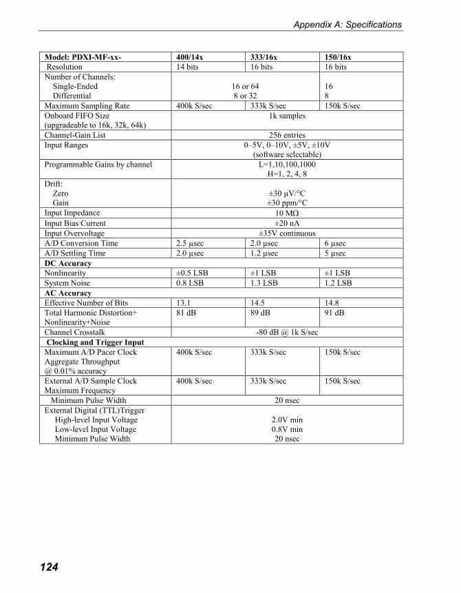
Appendix A: Specifications
124
Model: PDXI-MF-xx- 400/14x 333/16x 150/16x
Resolution 14 bits 16 bits 16 bits
Number of Channels:
Single-Ended
Differential
16 or 64
8 or 32
16
8
Maximum Sampling Rate 400k S/sec 333k S/sec 150k S/sec
Onboard FIFO Size
(upgradeable to 16k, 32k, 64k)
1k samples
Channel-Gain List 256 entries
Input Ranges 0–5V, 0–10V, ±5V, ±10V
(software selectable)
Programmable Gains by channel L=1,10,100,1000
H=1, 2, 4, 8
Drift:
Zero
Gain
±30 µV/°C
±30 ppm/°C
Input Impedance 10 MΩ
Input Bias Current ±20 nA
Input Overvoltage ±35V continuous
A/D Conversion Time 2.5 µsec 2.0 µsec 6 µsec
A/D Settling Time 2.0 µsec 1.2 µsec 5 µsec
DC Accuracy
Nonlinearity ±0.5 LSB ±1 LSB ±1 LSB
System Noise 0.8 LSB 1.3 LSB 1.2 LSB
AC Accuracy
Effective Number of Bits 13.1 14.5 14.8
Total Harmonic Distortion+
Nonlinearity+Noise
81 dB 89 dB 91 dB
Channel Crosstalk -80 dB @ 1k S/sec
Clocking and Trigger Input
Maximum A/D Pacer Clock
Aggregate Throughput
@ 0.01% accuracy
400k S/sec 333k S/sec 150k S/sec
External A/D Sample Clock
Maximum Frequency
400k S/sec 333k S/sec 150k S/sec
Minimum Pulse Width 20 nsec
External Digital (TTL)Trigger
High-level Input Voltage
Low-level Input Voltage
Minimum Pulse Width
2.0V min
0.8V min
20 nsec

Appendix A: Specifications
125
Analog Outputs - all PDXI-MF models
Number of Channels 2
Resolution 12 bits
Update Rate 200k S/sec each
Onboard FIFO Size 2k samples (on DSP)
Analog Output Range ±10V
Error
Gain ±1 LSB
Zero Calibrated to 0
Current Output ±20 mA max
Output Impedance 0.3W typ
Capacitive Drive Capability 1000 pF
Nonlinearity ±1 LSB
Protection Short circuit to analog ground
Power-on Voltage 0V ±10 mV
Setting Time to 0.01% of FSR 10 µsec, 20V step
1 µsec, 100-mV step
Slew Rate 30 V/µsec
Digital I/O - all PDXI-MF models
Input Bits
(8 can generate IRQ)
16
Output Bits 16
Inputs:
High-level Input Voltage
Low-level Input Voltage
High-level Input Current
Low-level Input Current
2.0V min
0.8V max
20 µA
-20 µA
Outputs:
Output Driver High Voltage
Output Driver Low Voltage
2.5V min, 3.0V typ (IOH = -32 mA)
0.55V max (IOL = 64 mA)
Current Sink -32/64 mA max, 250 mA per port
Pulse Width 20 nsec min, interrupt bit latched on
rising, falling or either edge
Power-on Voltage Logic Zero

Appendix A: Specifications
126
Counter/Timer - all PDXI-MF models
Number of Counters 3 available to user (Intel 82C54)
Resolution 16 bits on each counter
Clock Inputs:
Software configurable
High-level Input voltage
Low-level Input voltage
High-level Input current
Low-level Input current
Internal, 1M S/sec,
External, 10M S/sec
2.0V min
0.8V max
20 µA
-20 µA
Gate Inputs:
Maximum Pulse Width
100 nsec (High), 100 nsec (Low)
Counter Outputs:
Output Driver High Voltage
Output Driver Low Voltage
Inverted
2.5V min (IOH = 24 mA)
0.55V max (IOH = 48 mA)
General Specifications and Connectors – all PDXI-MF models
Power Requirements 5V
Physical Dimensions 7 x 4” (177 x 101 mm)
Environmental:
Operating Temperature Range
Storage Temperature Range
Relative Humidity
0 to 70°C
-25 to 85°C
to 95%, noncondensing
Connector J1 96-pin high-density Fujitsu connector (male)
(Fujitsu PN# FCN-245P096-G/U)
Connector J2 80-pin header connector (male)
(Adam Tech PN# HBMR-A-80-VSG)

Appendix A: Specifications
127
PDXI-MFS Simultaneous Sampling Boards
Model: PDXI-MFS-xx- 2M/14 1M/12 800/14
Resolution 14 bits 12 bits 14 bits
Number of Channels
Single-Ended
Differential (optional)
4 or 8
4 or 8
Maximum Sampling Rate
(multiple channels)
2M S/sec 1M S/sec 800k S/sec
Onboard FIFO Size
(upgradeable to 16k, 32k, 64k)
4k samples 1k samples
Input Ranges 0–5V, ±5V, 0–8V,
±8V @ 10V ranges
0–5V, 0–10V, ±5V, ±10V
(software selectable)
Channel-Gain List 256 entries
Programmable Gains by channel 1, 2, 5, 10
Drift
Zero
Gain
±30 µV/°C
±30 ppm/°C
Input Impedance 1 MΩ
Input Bias Current ±100 pA
Input Overvoltage ±18V SE
±40V DI
A/D Conversion Time 0.45 µsec 0.8 µsec 1.25 µsec
SSH Amp Settling Time 0.7 µsec 0.9 µsec 1.0 µsec
A/D Settling Time 0.4 µsec 0.6 µsec 1.25 µsec
DC Accuracy
Nonlinearity
(no missing codes)
±2 LSB ±0.5 LSB
AC Accuracy
Effective Number of Bits 12.1 11.3 12.7
Channel Crosstalk -80 dB @ 1k S/sec
Clocking and Trigger Input
Maximum A/D Pacer Clock 1500k S/sec @ 4 ch,
1700k S/sec @ 8 ch
975k S/sec @ 4 ch,
1095k S/sec @ 8 ch
800k S/sec
External A/D Sample Clock
Maximum Frequency
1500k S/sec @ 4 ch
1700k S/sec @ 8 ch
975k S/sec @ 4 ch,
1095k S/sec @ 8 ch
800k S/sec
Minimum Pulse Width 20 ns
External Digital (TTL)Trigger
High-level Input Voltage
Low-level Input Voltage
Minimum Pulse Width
2.0V min
0.8V min
20 nsec

Appendix A: Specifications
128
Model: PDXI-MFS-xx- 500/16 500/14 300/16
Resolution 16 bits 14 bits 16 bits
Number of Channels
Single-Ended
Differential (optional)
4 or 8
4 or 8
Maximum Sampling Rate
(multiple channels)
500k S/sec 300k S/sec
Onboard FIFO Size
(upgradeable to 16k, 32k, 64k)
1k samples
Input Ranges 0–5V, 0–10V, ±5V, ±10V
(software selectable)
Channel-Gain List 256 entries
Programmable Gains by channel 1, 2, 5, 10
Drift
Zero
Gain
±30 µV/°C
±30 ppm/°C
Input Impedance 1 MΩ
Input Bias Current ±100 pA
Input Overvoltage ±18V SE
±40V DI
A/D Conversion Time 2 µsec 2.0 µsec 3 µsec
SSH Amp Settling Time 1.2 µsec 1.2 µsec 1.2 µsec
A/D Settling Time 1.5 µsec 1.2 µsec 2.7 µsec
DC Accuracy
Nonlinearity
(no missing codes)
±1 LSB
AC Accuracy
Effective Number of Bits 13.8 12.7 13.8
Channel Crosstalk -80 dB @ 1k S/sec
Clocking and Trigger Input
Maximum A/D Pacer Clock 500k S/sec 300k S/sec
External A/D Sample Clock
Maximum Frequency
500k S/sec
300k S/sec
Minimum Pulse Width 20 nsec
External Digital (TTL)Trigger
High-level Input Voltage
Low-level Input Voltage
Minimum Pulse Width
2.0V min
0.8V min
20 nsec

Appendix A: Specifications
129
Analog Outputs—all PDXI-MFS models
Number of Channels 2
Resolution 12 bits
Update Rate 200k S/sec each
Onboard FIFO Size 2k samples (on DSP)
Analog Output Range ±10V
Error
Gain ±1 LSB
Zero Calibrated to 0
Current Output ±20 mA max
Output Impedance 0.3W typ
Capacitive Drive Capability 1000 pF
Nonlinearity ±1 LSB
Protection Short circuit to analog ground
Power-on Voltage 0V ±10 mV
Setting Time to 0.01% of FSR 10 µsec, 20V step
1 µsec, 100-mV step
Slew Rate 30 V/µsec
Counter/Timer—all PDXI-MFS models
Number of Counters 3 available to user
(Intel 82C54)
Resolution 16 bits on each counter
Clock Inputs
Software configurable
High-level Input voltage
Low-level Input voltage
High-level Input current
Low-level Input current
Internal, 1M S/sec
External, 10M S/sec
2.0V min
0.8V max
20 µA
-20 µA
Gate Inputs
Maximum Pulse Width
100 nsec (High), 100 nsec
(Low)
Counter Outputs
Output Driver High Voltage
Output Driver Low Voltage
Inverted
2.5V min (IOH = 24 mA)
0.55V max (IOH = 48 mA)

Appendix A: Specifications
130
Digital I/O—all PDXI-MFS models
Input Bits
(8 can generate IRQ)
16
Output Bits 16
Inputs
High-level Input Voltage
Low-level Input Voltage
High-level Input Current
Low-level Input Current
2.0V min
0.8V max
20 µA
-20 µA
Outputs:
Output Driver High Voltage
Output Driver Low Voltage
2.5V min, 3.0V typ (IOH = -32 mA)
0.55V max (IOL = 64 mA)
Current Sink -32/64 mA max, 250 mA per port
Pulse Width 20 ns min, interrupt bit latched on rising,
falling or either edge
Power-on Voltage logic Zero
General Specifications and Connectors - all PDXI-MFS models
Power Requirements 5V
Physical Dimensions 7 x 4” (177 x 101 mm)
Environmental:
Operating Temperature Range
Storage Temperature Range
0 to 70°C
-25 to 85°C
Relative Humidity to 95%, noncondensing
Connector J1 96-pin high-density Fujitsu connector (male)
(Fujitsu PN#FCN-245P096-G/U)
Connector J2 80-pin header connector (male)
(Adam Tech PN# HBMR-A-80-VSG)

Appendix A: Specifications
131

132
Appendix B: PowerDAQ A/D
Timing The following tables are intended to help you determine the fastest acquisition rates for various
models when working with various gains.
In the Board Model column, note that an “x” is a placeholder for various models and represents
the number of channels on the board.
In the Resolution / Speed / Gain column, “Low” refers to a board with modest gain capabilities
(either 1, 2, 4, 8 or 1, 2, 5, 10) and are intended to work with high-level signals—and hence the
“H” suffix on the board model number. Conversely, “High” in the second column refers to a board
with high gain capabilities (1, 10, 100, 1000) and are intended to work with low-level signals—
and hence the “L” suffix on the board model number.
The column “Fast Acq Delay” gives the minimum time between conversions when the board is
digitizing at its maximum rate.
The column “Slow Acq Delay (using Slow Bit)” gives the minimum time between conversions
when you activate the Slow Bit for a channel. Recall that a Slow Bit setting instructs the board to
wait an extra amount of time before taking the next sample, thereby giving the amplifier and other
front-end elements time to settle to the next value before actually digitizing the signal. This
column tells you exactly how much time you can expect to wait until the next channel is digitized.
Note We are working constantly to improve these specifications, and so they are subject to change. Please
check with the factory for the latest values.

Appendix B: PowerDAQ A/D Timing
133
PD2-MF Series Timing
Board Model Resolution / Speed /
Gain
Fast Acq
Delay
Slow Acq Delay
(using Slow Bit)
PD2-MF-xx-3M/12L 12 / 3 MHz / High 283 nsec 800 µsec
PD2-MF-xx-3M/12H 12 / 3 MHz / Low 283 nsec 800 µsec
PD2-MF-xx-2M/14H 14 / 2.2 MHz / Low 450 nsec 3.0 µsec
PD2-MF-xx-500/16L 16 / 500 kHz / High 2.0 µsec 20 µsec
PD2-MF-xx-500/16H 16 / 500 kHz / Low 2.0 µsec 10 µsec
PD2-MF-xx-400/14L 14 / 400 kHz / High 2.5 µsec 25.0 µsec
PD2-MF-xx-400/14H 14 / 400 kHz / Low 2.5 µsec 10.0 µsec
PD2-MF-xx-333/16L 16 / 333 kHz / High 3.0 µsec 20.0 µsec
PD2-MF-xx-333/16H 16 / 333 kHz / Low 3.0 µsec 10.0 µsec
PD2-MF-16-150/16L 16 / 150 kHz / High 6 µsec 20 µsec
PD2-MF-16-150/16H 16 / 150 kHz / Low 6 µsec 10 µsec
PD2-MFS Series Timing
Board Model Resolution /
Speed
Fast Acq
Delay
Slow Acq Delay
(using Slow Bits)
SSH Acq
Delay
SSH Hold
Delay
PD2-MFS-x-2M/14 14 / 2.2 MHz 450 nsec 2.0 µsec 700 nsec 500 nsec
PD2-MFS-x-800/14 14 / 800 kHz 1.25 µsec 3.0 µsec 900 nsec 700 nsec
PD2-MFS-x-500/14 14 / 500 kHz 2.0 µsec 3.0 µsec 900 nsec 700 nsec
PD2-MFS-x-333/16 16 / 333 kHz 3.0 µsec 10.0 µsec 900 nsec 700 nsec
PDL-MF Series Timing
Board Model Resolution / Speed / Gain Fast Acq
Delay
Slow Acq Delay (no
Slow Bits)
PDL-MF/PDL-MF-50 16 / 50 kHz / 1,2,5,10 20 µsec N/A
PDL-MF-333 16 / 333 kHz / 1,2,5,10 3 µsec N/A

Appendix B: PowerDAQ A/D Timing
134
PDXI-MF Series Timing
Board Model Resolution / Speed /
Gain
Fast Acq
Delay
Slow Acq Delay
(using Slow Bits)
PDXI-MF-xx-2M/14H 14 / 1.65 MHz / Low 450 nsec 3.0 µsec
PDXI-MF-xx-1M/12L 12 / 1.25 MHz / High 800 nsec 20.0 µsec
PDXI-MF-xx-1M/12H 12 / 1.25 MHz / Low 800 nsec 5.0 µsec
PDXI-MF-xx-800/14L 14 / 800 kHz / High 1.25 µsec 20.0 µsec
PDXI-MF-xx-800/14H 14 / 800 kHz / Low 1.25 µsec 10.0 µsec
PDXI-MF-xx-500/16L 16 / 500 kHz / High 2.0 µsec 20.0 µsec
PDXI-MF-xx-500/16H 16 / 500 kHz / Low 2.0 µsec 10.0 µsec
PDXI-MF-xx-400/14L 14 / 400 kHz / High 2.5 µsec 25.0 µsec
PDXI-MF-xx-400/14H 14 / 400 kHz / Low 2.5 µsec 10.0 µsec
PDXI-MF-xx-333/16L 16 / 333 kHz / High 3.0 µsec 20.0 µsec
PDXI-MF-xx-333/16H 16 / 333 kHz / Low 3.0 µsec 10.0 µsec
PDXI-MF-xx-150/16L 16 / 150 kHz / High 6.0 µsec 20.0 µsec
PDXI-MF-xx-150/16H 16 / 150 kHz / Low 6.0 µsec 10.0 µsec
PDXI-MF-xx-100/16L 16 / 100 kHz / Low 10.0 µsec 50.0 µsec
PDXI-MF-xx-100/16H 16 / 100 kHz / High 10.0 µsec 50.0 µsec
PDXI-MFS Series Timing
Board Model Resolution /
Speed
Fast Acq
Delay
Slow Acq
Delay (using
Slow Bits)
SSH Acq
Delay
SSH Hold
Delay
PDXI-MFS-x-2M/14 14 / 2.2 MHz 450 nsec 2.0 µsec 700 nsec 500 nsec
PDXI-MFS-x-1M/12 12 / 1.25 MHz 800 nsec 2.0 µsec 700 nsec 500 nsec
PDXI-MFS-x-800/14 14 / 800 kHz 1.25 µsec 3.0 µsec 900 nsec 700 nsec
PDXI-MFS-x-500/14 14 / 500 kHz 2.0 µsec 3.0 µsec 900 nsec 700 nsec
PDXI-MFS-x-333/16 16/ 333 kHz 3.0 µsec 10.0 µsec 900 nsec 700 nsec

Appendix B: PowerDAQ A/D Timing
135

136
Appendix C: Accessories UEI supplies a wide range of accessories for the PowerDAQ PD2/PDXI boards. They greatly
expand the core functionality of standard MF(S) hardware and allow you to employ these cards in
very demanding applications. These accessories also provide the means for implementing custom
interconnection schemes for OEM applications.
Screw-Terminal Panels (PD2/PDXI)
PD/PDXI-STP-96 Screw-terminal panel with 96- and 37-pin connector, suited for boards with as
many as 64 analog channels
PD/PDXI-STP-96-KIT Complete kit: Includes PD-STP-96, PD-CBL-96 and PD-CBL-37 for
64-channel boards
PD/PDXI-STP-9616 Screw-terminal panel with 96-pin and 37-pin connector for 4/8/16-channel
boards
PD/PDXI-STP-9616-KIT Complete kit: Includes PD-STP-9616, PD-CBL-96 and PD-CBL-37 for
4/8/16-channel boards
PD-STP-3716 Low-cost screw-terminal panel with 37-pin connector for 16-channel boards
PD-STP-3716-KIT Complete kit: Includes PD-STP-3716 and PD-CBL-9637 for 16-channel
boards
PD-STP-DIO Screw-terminal panel with 37-pin connector, handles digital I/O and
counter/timer signals only.
Screw Terminal Panels (PDL-MF only)
PDL-STP 100-way screw terminal with dual 50-pin IDC connectors
PDL-CBL-100 18” cable, connects 100-way connector on PDL-MF board and is terminated
with dual 50-way IDC connectors for the PDL-STP
PDL-MF-CONN Connector for direct attachment of signal leads to PDL-MF board, no cable
required
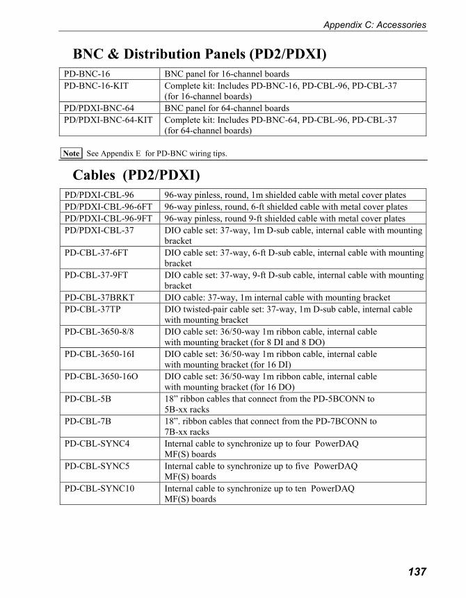
Appendix C: Accessories
137
BNC & Distribution Panels (PD2/PDXI)
PD-BNC-16 BNC panel for 16-channel boards
PD-BNC-16-KIT Complete kit: Includes PD-BNC-16, PD-CBL-96, PD-CBL-37
(for 16-channel boards)
PD/PDXI-BNC-64 BNC panel for 64-channel boards
PD/PDXI-BNC-64-KIT Complete kit: Includes PD-BNC-64, PD-CBL-96, PD-CBL-37
(for 64-channel boards)
Note See Appendix E for PD-BNC wiring tips.
Cables (PD2/PDXI)
PD/PDXI-CBL-96 96-way pinless, round, 1m shielded cable with metal cover plates
PD/PDXI-CBL-96-6FT 96-way pinless, round, 6-ft shielded cable with metal cover plates
PD/PDXI-CBL-96-9FT 96-way pinless, round 9-ft shielded cable with metal cover plates
PD/PDXI-CBL-37 DIO cable set: 37-way, 1m D-sub cable, internal cable with mounting
bracket
PD-CBL-37-6FT DIO cable set: 37-way, 6-ft D-sub cable, internal cable with mounting
bracket
PD-CBL-37-9FT DIO cable set: 37-way, 9-ft D-sub cable, internal cable with mounting
bracket
PD-CBL-37BRKT DIO cable: 37-way, 1m internal cable with mounting bracket
PD-CBL-37TP DIO twisted-pair cable set: 37-way, 1m D-sub cable, internal cable
with mounting bracket
PD-CBL-3650-8/8 DIO cable set: 36/50-way 1m ribbon cable, internal cable
with mounting bracket (for 8 DI and 8 DO)
PD-CBL-3650-16I DIO cable set: 36/50-way 1m ribbon cable, internal cable
with mounting bracket (for 16 DI)
PD-CBL-3650-16O DIO cable set: 36/50-way 1m ribbon cable, internal cable
with mounting bracket (for 16 DO)
PD-CBL-5B 18” ribbon cables that connect from the PD-5BCONN to
5B-xx racks
PD-CBL-7B 18”. ribbon cables that connect from the PD-7BCONN to
7B-xx racks
PD-CBL-SYNC4 Internal cable to synchronize up to four PowerDAQ
MF(S) boards
PD-CBL-SYNC5 Internal cable to synchronize up to five PowerDAQ
MF(S) boards
PD-CBL-SYNC10 Internal cable to synchronize up to ten PowerDAQ
MF(S) boards

Appendix C: Accessories
138
Mating cables, connectors, rack mounts (PD2/PDXI)
PD-CONN Mating connector with metal cover (includes Fujitsu
PN# FCN-230C096-C/E and FCN-247J096-G/E). Allows users to create
custom connector pinouts from PowerDAQ board.
PD-CONN-CBL 96-way pinless, 0.5m, round shielded cable with
metal cover plate (bare wires at one end)
PD-CONN-PCB PowerDAQ mating connector with pc-board attached
PD-CONN-9696 PowerDAQ connector for interfacing to custom/OEM boxes or equipment.
PD-CONN-NI Converts 100-way NI multipurpose analog-digital connector to the
PowerDAQ 96-way analog and 37-way digital connectors
PD-CONN-STR Individual Fujitsu connector (PN FCN-244P096-G/E), with a vertical pc-
board mount
PD-CONN-RTA Individual Fujitsu connector (PN FCN-245P096) with a right-angle
pc-board mount (version used on PowerDAQ boards)
PD-19RACK 19” rack, holds 3.5” deep terminal panels such as the PD-STP-96,
PD-STP-9616, and PD-BNC-16
PD-19RACKW 19” rack, wide version holds 7” deep terminal panels such as the
PD-TCR-16-x or PD-BNC-64
PD-5BCONN Connects 16- or 64-channel PowerDAQ board to one to four
5B-xx racks
PD-7BCONN Connects 16- or 64-channel PowerDAQ board to one to four
7B-xx racks
PD-100HDR Connects 16- or 64-channel PowerDAQ board to two 50-way IDC headers

Appendix C: Accessories
139
Signal Conditioning (all boards)
PD-PSU-5/15 Power supply (110/200V ac in; 5V, ±5V dc out) for use with PD-TCR-
16-x racks or with PD-ASTPs
PD-SCXU-AOMUX 8-channel analog-output multiplexer
PD-ASTP-16 16-channel AIn active screw-terminal panel (G = 1, 6-dB
cutoff @ 100 Hz)
PD-ASTP-16X 16-channel ASTP panel that adds 2 analog excitation-voltage channels
PD-ASTP-16SG Precision version of ASTP-16X with G = 100, cutoff of 10 Hz, for use
with strain gages and thermocouples
PD-5B-CONN Connects 64-channel PowerDAQ board to four ASTPs
PD2-DIO-BPLANE16 16-channel backplane for solid-state relay modules
PD2-DIO-CONN64-4 Distribution board (converts 100-way connector to four
50-way IDC headers)
PD2-DIO-CBL-100 100-way 1m cable
PD2-DIO-CBL-50 18” 50/50-way IDC ribbon cable, connects
PD2-DIO-CONN64-4 to PD2-DIO-BPLANE16
PD-5B-04 2-channel backplane, mounts 5B analog I/O modules to
MF(S) boards
PD-5B-08 8-channel backplane, mounts 5B analog I/O modules to
MF(S) boards
PD-5B-01 16-channel backplane, mounts 5B analog I/O modules to
MF(S) boards
Note UEI supplies a wide range of analog and digital signal-conditioning modules for use on these racks.
The list is far too extensive to publish in this manual. For the latest list, contact the factory or your
local distributor, or review the list on our web site at www.ueidaq.com.
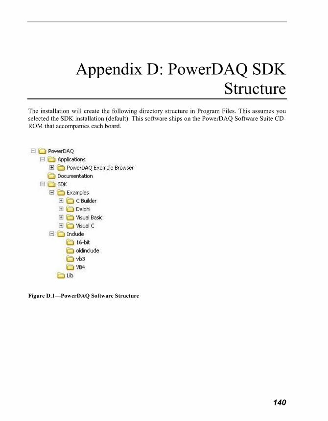
140
Appendix D: PowerDAQ SDK
Structure The installation will create the following directory structure in Program Files. This assumes you
selected the SDK installation (default). This software ships on the PowerDAQ Software Suite CD-
ROM that accompanies each board.
Figure D.1—PowerDAQ Software Structure
Appendix D: PowerDAQ SDK Structure
141
PowerDAQ Windows device drivers
Windows 9x
\windows\system pwrdaq95.vxd
Windows NT
\winnt\system32\drivers pwrdaq.sys
Windows 2000
\winnt\system32\drivers PwrDAQ2K.sys
\winnt\inf PwrDAQ2K.inf
Windows XP
\windows\system32\drivers PwrDAQ2K.sys
\windows\inf PwrDAQ2K.inf
Note The PDL-MF works on all operating systems except Windows 9x, and it also runs under Linux and
QNX. The PowerDAQ Software Suite Version 3 or above is required.
PowerDAQ Windows DLLs
The PowerDAQ Software Suite includes various DLLs (dynamic linked libraries) for different
versions of the Windows operating system. The location of these DLLs is as follows:
Windows 9x
\windows\system PwrDAQ32.dll (32-bit)
PwrDAQ16.dll (16-bit)
Windows NT/2000
\winnt\system32 PwrDAQ32.dll
PwrDAQ16.dll
Windows XP
\windows\system32 PwrDAQ32.dll
PwrDAQ16.dll
The DLLs have identical names for Windows 9x and NT/2000/XP, but note that they are
implemented differently. Both support the same API, so PowerDAQ applications that don’t use
functions specific to Win9x or WinNT/2000/XP should run on any version of Windows.

Appendix D: PowerDAQ SDK Structure
142
PowerDAQ Language Libraries
PowerDAQ SDK contains libraries for all major software development tools.
/lib
pwrdaq32.lib MSVC/MSVS v.5.x, 6.x
pd32bb.lib Borland C Builder v.3.0, 4.0
pd16bb.lib 16-bit Borland compilers
pwrdaq16.lib 16-bit MSVC 1.5x

Appendix D: PowerDAQ SDK Structure
143
PowerDAQ Include Files
/include
aliases.bas auxiliary functions to access PowerDAQ structures from within VB
DAQDefs.bas DAQ constant and variable definitions file for Visual Basic
DAQDefs.pas DAQ constant and variable definitions file for Delphi
pdApi.bas module used in SimpleTest VB example
pd_dsp_ct.h DSP counter-timer register definitions file for C/C++
pd_dsp_ct.pas DSP counter-timer register definitions file for Delphi
pd_dsp_es.h ESSI port register definitions file for C/C++
pd_dsp_es.pas ESSI port register definitions file for Delphi
pd32hdr.h PowerDAQ DLL driver interface function definitions file for C\C++
pd32hdr.pas PowerDAQ DLL driver interface function definitions file for Delphi
pdfw_bitsdef.bas PowerDAQ Firmware Command definitions file for Visual Basic
pdfw_bitsdef.pas PowerDAQ Firmware Command definitions file for Delphi
pdfw_def.h firmware constant definition file for C/C++
pdfw_def.pas firmware constant definition file for Borland Delphi
pdfw_def.bas firmware constant definition file for Visual Basic
pd_hcaps.h boards capabilities definition file for C/C++
pd_hcaps.pas PowerDAQ Firmware PCI interface definitions file for Visual Basic
pdpcidef.h PowerDAQ Firmware PCI interface definitions file for C\C++
pdpcidef.pas PowerDAQ Firmware PCI interface definitions file for Delphi
pwrdaq.h driver constants and definitions file for C/C++
pwrdaq.pas driver constants and definitions file for Delphi
pwrdaq.bas driver constants and definitions file for Visual Basic
pwrdaq32.h API function prototypes and structures file for C
pwrdaq32.hpp API function prototypes and structures file for C++
pwrdaq32.pas API function prototypes and structures file for Delphi
pwrdaq32.bas API function prototypes and structures file for Visual Basic
pxi.bas PXI related function definitions file for Visual Basic
pxi.h PXI related function definitions file for C\C++
sigproc.h PowerDAQ FFT and windows routines definition file for C
sigproc.hpp PowerDAQ FFT and windows routines definition file for C++

Appendix D: PowerDAQ SDK Structure
144
vbdll.bas auxiliary functions to access PowerDAQ buffer from within VB
/include/vb3
pwrdaq16.bas API function prototypes and structures file for Visual Basic v.3.0
pdfw_def.bas firmware constant definition file for Visual Basic v.3.0
pd_hcaps.bas boards capabilities definition file for Visual Basic v.3.0
daqdefs.bas event word definition for Visual Basic v.3.0
/include/16-bit
pwrdaq16.h API function prototypes and structures file for 16-bit C/C++
pwrdaq.h driver constants and definitions file for 16-bit C/C++
pdd_vb3.h auxiliary functions to access PowerDAQ structures from within VB
v.3.0
pd_hcaps.h boards capabilities definition file for 16-bit C
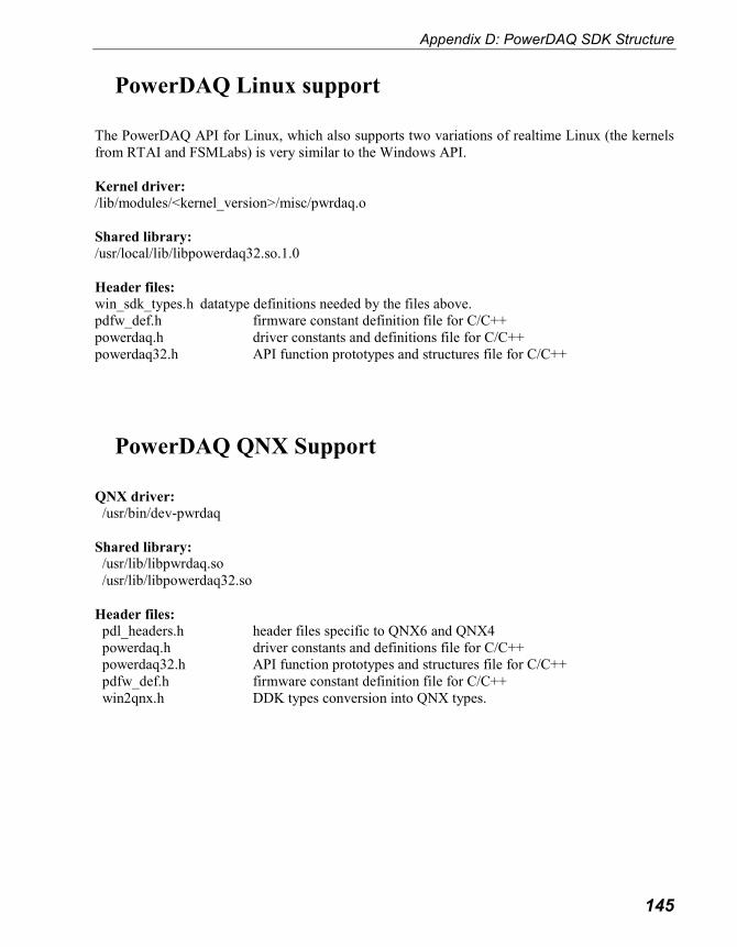
Appendix D: PowerDAQ SDK Structure
145
PowerDAQ Linux support
The PowerDAQ API for Linux, which also supports two variations of realtime Linux (the kernels
from RTAI and FSMLabs) is very similar to the Windows API.
Kernel driver:
/lib/modules/<kernel_version>/misc/pwrdaq.o
Shared library:
/usr/local/lib/libpowerdaq32.so.1.0
Header files:
win_sdk_types.h datatype definitions needed by the files above.
pdfw_def.h firmware constant definition file for C/C++
powerdaq.h driver constants and definitions file for C/C++
powerdaq32.h API function prototypes and structures file for C/C++
PowerDAQ QNX Support
QNX driver:
/usr/bin/dev-pwrdaq
Shared library:
/usr/lib/libpwrdaq.so
/usr/lib/libpowerdaq32.so
Header files:
pdl_headers.h header files specific to QNX6 and QNX4
powerdaq.h driver constants and definitions file for C/C++
powerdaq32.h API function prototypes and structures file for C/C++
pdfw_def.h firmware constant definition file for C/C++
win2qnx.h DDK types conversion into QNX types.
146
Appendix E: Application Notes
1. PowerDAQ Advanced Circular Buffer (ACB)
The Advanced Circular Buffer (ACB) solves many of the problems associated with high-
throughput data acquisition on a multithreaded /multitasking operating system. For simplicity, data
acquisition as an input process is discussed here. However, the same concepts can be applied to
output-signal generation.
• Asynchronous operation
• Nondeterministic processor time slots per thread
• Dynamic processor loading
• Nondeterministic user operation
The ACB requires that the DAQ interface library allocate a large circular buffer in the
application's memory space. The buffer size must be no larger than the available physical memory
with sufficient physical memory left over for most of the executable portion of the OS and active
applications to reside in memory. This prevents code or data from frequently being swapped to
disk. Consequently, if continuous gap-free acquisition is to be performed, the buffer should be
large enough to hold all the acquired data for the maximum time period expected between
application execution latency and the time required for the application to process all data in a full
buffer. This also implies that the application must be able to process the data at a rate faster than
the rate of acquisition.
Once acquisition is started, the DAQ board/driver transfer and store data into the buffer at one
rate, and the application generally reads the data from the buffer at another rate. Both operations
occur asynchronously of each other.

Appendix E: Application Notes
147
Frame Markers
Buffer Tail
Buffer Head
Board/Driver
Write New Data
At Buffer Head
Application
Reads Data From
Buffer Tail
Driver Asserts
Frame Done Events
When Data Written
Passes FrameBoundry
Advanced Circular
Buffer
Figure E.1—Advanced Circular Buffer
The application can be synchronized to the acquisition process by either timer notification or by an
event from the driver notifying that a certain sample count boundary has been passed.
In order to receive notification on a sample or scan count boundary, the buffer is segmented into
frames. Whenever the data transferred to the buffer crosses a frame boundary, the driver sends an
event to the application. This event wakes up the application thread that is responsible for
processing data in the buffer. To keep the frame boundaries at fixed buffer locations, the buffer
size should be a multiple of the frame size. If multichannel acquisition is performed, then the
frame size should also be a multiple of the scan size. Doing so keeps the pointer arithmetic from
becoming unnecessarily complex.
With the ACB, three modes of operation are possible:
• Single Buffer
• Circular Buffer
• Recycled Circular Buffer
In all three modes, data is written to the beginning of the buffer at the start of acquisition. The
three modes differ in what is done when the end of the buffer is reached and if the buffer head
catches up with the buffer tail.

Appendix E: Application Notes
148
Single Buffer
In the Single Buffer mode, acquisition stops when the buffer end is reached. In this mode, the
application can access the buffer and process the data any time during acquisition or wait until the
buffer is full, and acquisition stops. The Single Buffer mode is the simplest to program, and it’s
also the most common. It is useful in applications where acquiring data in a continuous stream is
not required. This is similar to the way digital multimeters and storage scopes acquire signals,
whereby a single buffer is filled and then the waveform is displayed. This process can also be
repeated any number of times.
Circular Buffer
In the Circular Buffer mode, the buffer head and tail wrap to the beginning of the buffer when the
end is reached. Data is written at the location pointed to by head and the head pointer is
incremented, and likewise data is read from the location pointed to by the tail and the tail pointer
is incremented. When the head pointer wraps around and reaches the tail pointer, then the buffer is
considered full and acquisition stops with a buffer overflow condition. To prevent unintentional
incrementing of the tail pointer, the pointer should be incremented after the application has
finished reading the data in the buffer and has indicated that the buffer space is relinquished for
the write operation.
The Circular Buffer mode is useful in applications that must acquire data with no sample loss.
Each acquired sample must be stored by the hardware/driver and read by the application. The data-
acquisition operation continues until the application issues a stop command to the driver. If the
application cannot keep up with the acquisition process and the buffer overflows, then the
acquisition is stopped and the error condition is reported.
Recycled Circular Buffer
The Recycled Circular Buffer mode is similar to the Circular Buffer mode except that when the
head pointer catches up with the tail pointer, the tail pointer is automatically incremented to the
next frame boundary. This buffer-space recycling occurs irrespective of whether the application
read the data or not. In this mode, a buffer overflow condition never occurs.
The Recycled Circular Buffer is best suited for applications that monitor acquired signals at
periodic intervals. The application may require the signals to be acquired at a high rate, but not all
acquired samples need to be processed. Also, an application may only need the latest block of
samples acquired. As the buffer fills up, the driver is free to recycle frames, automatically
incrementing the buffer tail, and using the space to store new samples.
While the Advanced Circular Buffer may appear a much different buffering mechanism when
compared to the much simpler single and double buffer mechanisms, it is actually a superset of the
simpler buffers. The ACB configured in the single buffer mode will behave just as the simple
ordinary single buffer. If the ACB is configured as Circular Buffer with two frames, it will behave
as a double buffer. With multiple frames, the ACB can be used in algorithms that were designed
for buffer queues. The only limitation, which consequently results in more efficient performance,
is that the logical buffers in the buffer queues cannot be dynamically allocated and freed. In
addition, their order is fixed.

Appendix E: Application Notes
149
2. PD-BNC-xx wiring options:
Voltage dividers
To build a voltage divider, install resistors in the R0A, R8A and R0C positions for the Ch0 and
Ch8 pair, and similarly for other pairs. Note that when supplied by the factory, the RxA resistors
have 0Ω (wire) jumpers installed
Lowpass filtering
To build a lowpass filter, install resistors in the R0A and R8A positions. Also install a capacitor in
the C0B position for the Ch 0 and Ch 8 pair, and for other pairs as well. Note that when supplied
by the factory, the RxA resistors have 0Ω (wire) jumpers installed.
Highpass filtering
In order to build a highpass filter, install capacitors in the R0A and R8A positions. Also install a
resistor into the C0B position for the Ch 0 and Ch 8 pair and for other pairs as well. Note that
when supplied by the factory, the RxA resistors have 0Ω (wire )jumpers installed.

150
Appendix F: Warranty
All PowerDAQ boards have received CE Mark certification according to the following:
EN55011 Radiated Emissions Standard
EN50082-1 Generic Immunity Standard
UEI Terms and Conditions for all products are available as copies on demand, and
online at http://ueidaq.com/company/terms.aspx

151
Appendix G: Glossary
A
ACB see Advanced Circular Buffer
A/D (see ADC) Analog/digital, often used in connection with an A/D
converter.
adapter Alternate designation for a function card that plugs into a
backplane, often a PC.
ADC (also see A/D) Analog-to-Digital Converter. An integrated circuit that
converts an analog voltage to a digital number.
ADC conversion The process of converting an analog input to its digital
equivalent.
ADC conversion Start Signal used to start the process of converting an analog input
to a digital value. The source of this signal can be an internal
clock or an external asynchronous signal.
ADC Channel List Start Signal used to start the acquisition of digitized values as
defined in the Channel List. The triggering edge of this signal
(falling edge) enables the ADC conversion Start signals.
Advanced Circular Buffer A special user-defined buffer in host memory that stores
frames of collected data. The PowerDAQ driver allows the
user application to fetch data from this buffer in several
modes.
alias A false lower-frequency component that appears in sampled
data that has been acquired at an insufficiently high sampling
rate.
analog trigger A trigger that occurs when an analog signal reaches a user-
selected level. Users can configure triggering to occur at a
specific level on either an increasing or a decreasing signal
(positive or negative slope).
API Application Programming Interface, a collection of high-level
language function calls that provide access the functions in a
driver or other utility.
asynchronous (1) Hardware—A property of an event that occurs at an
arbitrary time, without synchronization to a reference clock.
Appendix G: Glossary
152
(2) Software—A property of a function that begins an
operation and returns prior to the completion or termination of
the operation.
B background acquisition Data is acquired by a DAQ system while another program or
processing routine is running without apparent interruption.
base address A memory address that serves as the starting address for
programmable registers. All other addresses are located by
adding to the base address.
bipolar A signal range that includes both positive and negative values
(for example, -5V to +5V, also represented as ±5V).
bit One binary digit, either 0 or 1.
Block mode A high-speed data transfer in which the address of the data is
sent followed by a specified number of back-to-back data
words.
Burst mode A high-speed data transfer in which the address of the data is
sent followed by back-to-back data words while a physical
signal is asserted.
bus The group of conductors that interconnect individual circuitry
in a computer. Typically, a bus is the expansion vehicle to
which I/O or other devices are connected. Examples of PC
buses are the PCI bus and the PXI bus.
bus master A type of plug-in board or controller that can read and write to
devices on the computer bus without the assistance of the host
CPU.
byte Eight related bits of data, an 8-bit binary number. Also used to
denote the amount of memory required to store one byte of
data.
C cache High-speed processor memory that buffers commonly used
instructions or data to increase processing throughput.
calibration The setting or correcting of a measuring device or base level,
usually by adjusting it to match or conform to a dependably
known and unvarying measure.
channel list A variable length list of from 1 to 256 entries, each of which
defines a channel, its gain any Slow Bits. In continuous A/D
acquisition mode, the list wraps around to the first channel
after it reaches the end. The channels need not be in any
particular order and may appear multiple times in the list.
Channel List FIFO The on-board memory that holds the Channel List.

Appendix G: Glossary
153
CL clock The Channel List clock, also known as the Burst clock, tells
the control logic how quickly to move to the next entry in the
Channel List and set up the front-end operating parameters
such as gain.
control register Register containing control bits that set up and configure
various onboard subsystems.
CMRR Common-Mode Rejection Ratio, a measure of an instrument's
ability to reject interference from a common-mode signal,
usually expressed in decibels (dB).
code generator A software program, controlled from an intuitive user
interface, that creates syntactically correct high-level source
code in languages such as C or Basic.
cold-junction compensation The means to compensate for the ambient temperature in a
thermocouple measurement circuit.
common-mode range The input range over which a circuit can handle a common-
mode signal.
common-mode signal The mathematical average voltage, relative to the computer's
ground, of the signals going into a differential input.
component software An application that contains one or more component objects
that can freely interact with other component software.
Examples
include OLE-enabled applications such as Microsoft Visual
Basic and OLE Controls.
conversion time The time, in an analog input or output system, from the
moment a channel is interrogated (such as with a Read
instruction) to the moment that accurate data is available.
counter/timer A circuit that counts external pulses or clock pulses (timing),
such as the Intel 8254 device.
coupling The manner in which a signal is connected from one location
to another.
crosstalk An unwanted signal on one channel due to an input on a
different channel.
current drive capability The amount of current a digital or analog output channel can
source or sink while still operating within voltage range
specifications.
current sinking The ability of a DAQ board to dissipate power from an output
signal, either analog or digital. Some sensors apply a voltage
to a loop, and the DAQ card must be able to accept the
resulting current flow.
current sourcing The ability of a DAQ board to supply current for analog or
digital output signals.

Appendix G: Glossary
154
CV clock The Conversion Clock, also known as the Pacer clock, it
triggers individual acquisitions and thus tells the A/D how fast
to digitize successive samples.
D D/A Digital-to-analog, digital/analog
DAC Digital-to-Analog Converter, an integrated circuit that
converts a digital value into a corresponding analog voltage or
current.
DAC conversion Start Signal used to start the process of converting a digital value to
an analog output. The source of this signal can be either an
internal synchronous clock or an external asynchronous signal.
DAQ Data Acquisition
(1) Collecting and measuring electrical signals from sensors,
transducers, and test probes or fixtures, and moving them to a
computer for processing;
(2) Collecting and measuring the same kinds of electrical
signals with A/D or DIO boards plugged into a PC, and
possibly generating control signals with D/A or DIO boards in
the same PC.
dB Decibel, the unit for expressing a logarithmic measure of the
ratio of two signal levels: dB = 20log10(V1/V2) for signals in
volts.
differential input An analog-input configuration that measures the difference
between signals on two terminals, both of which are isolated
from computer ground.
DIO Digital input/output.
DLL Dynamic Link Library, a software module in Microsoft
Windows containing executable code and data that can be
called or used by Windows applications or other DLLs.
Functions and data in a DLL are loaded and linked at run time
when they are referenced by a Windows application or other
DLLs.
DNL Differential nonlinearity, a measure in LSBs of the worst-case
deviation of code widths from their ideal value of 1 LSB.
DMA Direct Memory Access, a method of transferring data to/from
computer memory from/to a device or memory on the bus,
taking place while the host processor does something else.
DMA is the fastest method of transferring data to/from
computer memory.
drivers Software that controls a specific hardware device such as a
DAQ board.
Appendix G: Glossary
155
DSP Digital signal processing.
dual-access memory Memory that can be sequentially accessed by more than one
controller or processor but not simultaneously. Also known as
shared memory.
dual-port memory Memory that can be simultaneously accessed by more than
one controller or processor.
dynamic range The ratio, normally expressed in dB, of the largest signal level
in a circuit to the smallest signal level. In DAQ boards it
typically refers to the range of signals a board can handle or
the amount of noise it suppresses.
E EEPROM Electrically Erasable Programmable Read-Only Memory, a
nonvolatile memory device you can repeatedly program for
storage, erase and reprogram.
encoder A device that converts linear or rotary displacement into
digital or pulse signals. The most popular type of encoder is
the optical encoder.
EPROM Erasable Programmable Read-Only Memory: A nonvolatile
memory device that can be erased (usually by ultraviolet light
exposure) and reprogrammed.
event A signal or interrupt generated by a device to notify another
device of an asynchronous event. The contents of events are
device-dependent.
event-based mode A board operating mode whereby it notifies the user
application of certain predefined subsystem events using
Win32 calls. It allows you to write asynchronous applications.
external trigger A voltage pulse from an external source that triggers an event
such as an A/D conversion.
F FIFO First-In First-Out, usually used in reference to a memory
buffer where the first data stored is the first sent out.
fixed point A format for processing or storing numbers as digital integers.
In fixed-point arithmetic all numbers are represented by
integers, fractions (usually restricted between ±1.0) or a
combination of both integers and fractions. Thus integer
mathematics can be implemented on all general-purpose
processors.
floating point Representing data as a combination of a mantissa and an
exponent. The mantissa is usually described by a signed
fractional value that has a magnitude >= 1.0 and restricted to<
2.0. The exponent, instead, is an integer and represents the
Appendix G: Glossary
156
number of places any binary number must be shifted, left or
right, in order to yield the desired value.
frame A user-defined number of scans, and these datapoints reside in
a predefined portion of a buffer in host-memory. This host-
memory buffer is also known as the Advanced Circular Buffer
(ACB).
function A set of software instructions executed by a single line of code
that may have input and/or output parameters and returns a
value when executed.
G gain The factor by which a signal is amplified, sometimes
expressed in dB.
gain accuracy A measure of the deviation of an amplifier’s gain from the
ideal gain.
GUI Graphical User Interface, an intuitive means of
communicating information to and from a computer program
by means of graphical screen displays. GUIs can resemble the
front panels of instruments or other objects associated with a
computer program.
H handler A device driver installed as part of the computer’s OS.
hardware The physical components of a computer system, such as the
circuit boards, plug-in boards, chassis, enclosures, peripherals,
cables, and so on.
I IMD Intermodulation Distortion, the ratio, in dB, of the total RMS
signal level of harmonic sum and difference distortion
products, to the overall RMS signal level. The test signal
consists of two sinewaves added together.
INL Integral Nonlinearity, a measure in LSB of the worst-case
deviation from the ideal A/D or D/A transfer characteristic of
the analog I/O circuitry.
input bias current The current that flows into the inputs of a circuit.
input impedance The measured resistance and impedance between the input
terminals of a circuit.
input offset current The difference in the input bias currents of the two inputs of
an instrumentation amplifier.
instrumentation amplifier A circuit whose output voltage with respect to ground is
proportional to the difference between the voltages at its two
inputs.

Appendix G: Glossary
157
integral control A control action that eliminates the offset inherent in
proportional control.
integrating A/D An A/D whose output code represents the average value of the
input voltage over a given time interval.
interrupt A computer signal indicating that the CPU should suspend its
current task to service a designated activity.
I/O Input/Output, the transfer of data to/from a computer system
involving communications channels, operator interface
devices, and/or data-acquisition and control interfaces.
IPC Interprocess Communication, protocol by which processes can
pass messages. Messages can be either blocks of data and
information packets, or instructions and requests for
process(es) to perform actions. A process can send messages
to itself, other processes on the same machine, or processes
located anywhere on the network.
isolation voltage The voltage that an isolated circuit can normally withstand,
usually specified from input to input and/or from any input to
the amplifier output, or to the computer bus.
K k kilo, the standard metric prefix for 1000 or 10
3, used with
units of measure such as volts, Hertz, and meters.
L linearity The adherence of device response to the equation R = KS,
where R = response, S = stimulus, and K is a constant.
LSB Least-significant bit.
M M mega, the standard metric prefix for 1 million or 10
6, when
used with units of measure such as volts and Hertz; the prefix
for 1,048,576, or 220, when used to quantify data or computer
memory.
Mbytes/s A unit for data transfer that means 1 million or 106 bytes/sec.
MMI Man-machine interface, the means by which an operator
interacts with an industrial automation system; often called a
GUI.
multiplexer A switching device with multiple inputs that sequentially
connects each of its inputs to its output, typically at high
speeds, in order to measure several signals with a single
analog input channel.

Appendix G: Glossary
158
multitasking A property of an operating system in which several processes
can run simultaneously.
mux see multiplexer
N noise An undesirable electrical signal. Noise comes from external
sources such as the AC
power line, motors, generators, transformers, fluorescent
lights, soldering irons, CRT displays, computers, electrical
storms, welders, radio transmitters as well as internal sources
such as semiconductors, resistors and capacitors.
O OLE Object Linking and Embedding, a set of system services that
provides a means for applications to interact and interoperate.
Based on the underlying Component Object Model, OLE is
object-enabling system software. Through OLE Automation,
an application can dynamically identify and use the services of
other applications. OLE also makes it possible to create
compound documents consisting of multiple sources of
information from different applications.
OLE controls see ActiveX controls.
operating system Base-level software that controls a computer, runs programs,
interacts with users, and communicates with installed
hardware or peripheral devices.
optical isolation The technique of using an optoelectric transmitter and receiver
to transfer data without electrical continuity to eliminate high
potential differences and transients.
OS see operating system
output settling time The amount of time required for the analog output voltage of
an amplifier to reach its final value within specified limits.
output slew rate The rate of change of an analog output voltage from one level
to another.
overhead The amount of computer processing resources, such as time or
memory, required to accomplish a task.
P paging A technique used for extending the address range of a device
to point into a larger address space

Appendix G: Glossary
159
PCI Peripheral Component Interconnect, an expansion bus
architecture originally developed by Intel to replace ISA and
EISA. It offers a theoretical maximum transfer rate of 132M
bytes/sec.
PDXI PowerDAQ eXtensions for Instrumentation, UEI’s
implementation of the PXI bus standard.
PGA see Programmable-gain amplifier
PID control A 3-term control algorithm combining proportional, integral
and derivative control actions.
pipeline A high-performance processor structure in which the
completion of an instruction is broken into its elements so that
several elements can be processed simultaneously from
different instructions.
PLC Programmable logic controller, a special-purpose computer
used in industrial monitoring and control applications. PLCs
typically have proprietary programming and networking
protocols and special-purpose digital and analog I/O ports.
Polled mode DAQ board operating mode whereby the user application
queries the board about the status of various subsystems as
needed.
port A communications connection on a computer or a remote
controller.
postriggering The technique used on a DAQ board to acquire a programmed
number of samples after trigger conditions are met.
potentiometer An electrical device whose resistance you can manually
adjusted; known among engineers as a “pot.”
pretriggering The technique used on a DAQ board to keep a continuous
buffer filled with data, so that when the trigger conditions are
met, the sample includes the data leading up to the trigger
condition.
programmable-gain amplifier also see PGA, an amplifier where you can change the amount
of gain applied to the inputs. Gain settings today are usually
made with software instead of setting jumpers as was
necessary with first-generation DAQ boards.
programmed I/O The standard method a CPU uses to access an I/O device—
each byte of data is read or written by the CPU.
propagation delay The amount of time required for a signal to pass through a
circuit.
proportional control A control action whose output is proportional to the deviation
of the controlled variable from a desired setpoint.
protocol The exact sequence of bits, characters and control codes used
to transfer data between computers and peripherals through a
communications channel.
Appendix G: Glossary
160
pseudodifferential An analog-input configuration where all channels refer their
inputs to a common ground—but this ground is not connected
to the computer ground.
PXI PCI eXtensions for Instrumentation, a bus standard that
combines the mechanical form factor of the CompactPCI
specification and the electrical aspects of the PCI bus. It also
adds integrated timing and triggering designed specifically for
measurement and automation applications.
Q quantization error The inherent uncertainty in digitizing an analog value due to
the finite resolution of the conversion process.
R real time A system in which the desired action takes place immediately
when all input conditions are fulfilled; it never has to wait for
other processes to complete before it can start. In DAQ terms,
it generally refers to the processing of data as it is acquired
instead of being accumulated and getting processed at a later
time.
relative accuracy A measure in LSB of the accuracy of an A/D. It includes all
nonlinearity and quantization errors. It does not include offset
and gain errors of the circuitry feeding the ADC.
resolution The smallest signal increment that a measurement system can
detect. Resolution can be expressed in bits, in proportions, or
in percent of full scale. For example, a system has a resolution
equal to 12 bits = one part in 4,096 = 0.0244% of full scale.
resource locking A technique whereby a device is signaled not to use one of its
resources, often local memory, while that resource is being
used by another device, generally the system bus.
ribbon cable A flat cable in which conductors are placed side by side.
RMS Root-mean square, computed by squaring the instantaneous
voltage, integrating over the desired time and taking the
square root.
RTD Resistance temperature detectors operate based on the
principle that electrical resistance varies with temperature.
They generally use pure metal elements, platinum being the
most widely specified RTD element type although nickel,
copper, and Balco (nickel-iron) alloys are also used. Platinum
is popular due to its wide temperature range, accuracy,
stability as well as the degree of standardization among
manufacturers. RTDs are characterized by a linear positive
change in resistance with respect to temperature. They exhibit

Appendix G: Glossary
161
the most linear signal over temperature of any electronic
sensing device
RTSI Real Time Systems Integration bus, developed by National
Instruments, this intercard bus allows you to transfer data and
control signals without using the backplane bus.
S samples/sec expresses the rate at which a DAQ board digitizes an analog
signal.
scan one run through the presently configured Channel List
SDK Software developer’s kit, a collection of drivers and utilities
that allow engineers to write their own application programs.
SE see single-ended.
self-calibrating reference to a DAQ board that calibrates its own A/D and D/A
circuits with a reference source, sometimes provided internally
with a precision D/A converter.
sensor A device that generates an electrical signal in response to a
physical stimulus (such as heat, light, sound, pressure, motion
or flow).
S/H Sample/Hold, a circuit that acquires and stores an analog
voltage on a capacitor for a short period of time.
simultaneous sampling the act of digitizing multiple channels simultaneously, with
interchannel skew often being measured in psec.
single-ended a term used to describe an analog-input configuration where
you measure each channel with respect to a common analog
ground.
Slow Bit a control bit in the analog-input configuration word that
instructs the A/D to wait a short while before actually
digitizing the input voltage; it gives the input amplifier time to
settle, and is very useful when working with very high gains.
SNR also S/N ratio or Signal/Noise ratio, the ratio of the peak
power level to the remaining noise power, expressed in dB.
software trigger A programmed event that triggers an event such as a data
acquisition.
SPDT Single-pole double-throw, a switch in which one terminal can
be connected to one of two other terminals.
SSH Simultaneous Sample/Hold, see simultaneous sampling
S/s, S/sec see samples/sec
strain gage A sensor that converts mechanical motion into an electronic
signal. A change in capacitance, inductance or resistance is
proportional to the strain experienced by the sensor, but
Appendix G: Glossary
162
resistance is the most widely used characteristic that varies in
proportion to strain.
subroutine A set of software instructions executed by a single line of code
that may have input and/or output parameters.
subsystem On PowerDAQ cards, a group of circuits that perform either
analog input, analog output, digital input, digital output or
counter/timer functions.
successive-approximation A/D An A/D that sequentially compares a series of binary-
weighted values with an analog input to produce an output
digital word in n steps, where n is the A/D’s resolution in bits.
synchronous A property of a function that begins an operation and returns
only when the operation is complete.
system noise A measure of the amount of noise seen by an analog circuit or
an A/D when the analog inputs are grounded.
T TCP/IP Transmission Control Protocol/Internet Protocol, the basic 2-
layer communication protocol of the Internet but that is also
used in a private network (either an intranet or an extranet).
The higher layer, TCP, manages the assembling of a message
or file into smaller packets that are transmitted and received
by a TCP layer that reassembles the packets into the original
message. IP handles the address portion of each packet so it
gets to the right destination.
THD Total harmonic distortion, the ratio of the total RMS signal
due to harmonic distortion to the overall RMS signal,
expressed in dB or percent.
THD+N The percentage of Total Harmonic Distortion + Noise
(THD+N) of a sine wave equals 100 times the ratio of the
RMS voltage measured with the fundamental component of a
sine wave removed by a notch filter, to the RMS voltage of the
fundamental component.
thermistor A temperature-sensing element that exhibits a large change in
resistance proportional to a small change in temperature.
Thermistors usually have negative temperature coefficients.
They tend to be more accurate than thermocouples or RTDs,
but they have a much more limited temperature range.
thermocouple A temperature sensor created by joining two dissimilar metals.
The junction produces a small voltage as a function of
temperature.
throughput rate The flow of data, measured in bytes/sec, for a given
continuous operation.
Appendix G: Glossary
163
transducer A device that converts energy from one form to another.
Generally applied to devices that convert a physical
phenomenon (such as pressure, temperature, humidity or flow)
to an electrical signal.
transfer rate The rate, measured in bytes/sec, at which data is moved from a
source to a destination after software initialization and setup
operations; the maximum rate at which the hardware can
operate.
Trigger A signal, in either hardware or software, that initiates or halts
a process. In DAQ boards, it generally refers to a signal that
starts or stops an A/D, D/A or DIO operation.
U UCT User counter/timer
unipolar A signal range that is always positive (for example, 0 to 10 V).
Z zero offset The difference between true zero and an indication given by a
measuring instrument.
zero-overhead looping The ability of a high-performance processor to repeat
instructions without requiring time to branch to the beginning
of the instructions.
zero-Wait-State memory Memory fast enough that the processor does not have to wait
during any reads and writes to the memory.
Index
5
56301...................................................7, 105
5B modules............................................. 140
8
82C54 ................................................41, 103
A
A/D
peak rates ........................................... 133
successive approximation .................... 45
A/D FIFO............................................ 40, 64
ACB...............see Advanced Circular Buffer
Accessories ............................................. 137
Active screw-terminal panel ................... 140
Adapter ..................................................... 43
Advanced Circular Buffer64, 69, 79, 90, 147

Index
164
circular buffer mode .............................70
recycled mode ......................................70
single buffer mode................................70
Agilent VEE support...............................111
Analog output
1-shot waveform.............................86, 89
asynchronous........................................89
autoregeneration .............................86, 93
backward compatibility ........................94
Channel List .........................................87
clocking ................................................87
configuration bits..................................94
continuous waveform .....................86, 90
data conversion.....................................87
event based waveform....................86, 94
events ...................................................86
repetitive waveform........................86, 92
single update...................................85, 88
software command ...............................96
triggering ........................................88, 96
Analog output multiplexer ......................140
Analog-input subsystem......................39, 45
Analog-output subsystem....................40, 85
ASTP........ see Active Screw Terminal Panel
Averaging..................................................46
B
Base address..............................................23
Binary rate multiplier ..............................103
Block diagram, PD2-MF(S) ......................37
Block diagram, PDL-MF ..........................39
Block diagram, PDXI-MF(S)....................38
BNC panels .............................................138
Board families .............................................8
Board types .................................................8
Borland C++ examples............................110
Buffer size.................................................80
Burst buffered acquisition .........................76
Burst clock ............................... see CL clock
Bus mastering............................................64
C
C examples..............................................109
Cables, master list ...................................138
Calibration certificate................................15
Calibration procedures ..............................36
CE Mark Certification .............................151
Channel List ........................................45, 46
Channel List clock....................see CL clock
Channel List FIFO.....................................39
Circular Buffer mode.................................70
CL clock ..............................................22, 57
Clock
analog output ........................................87
CL clock ...................................22, 31, 57
configuration bits..................................58
continuous ............................................58
CV clock...................................22, 31, 57
default ...................................................58
external .................................................57
internal..................................................57
PDL-MF ...............................................59
software ................................................57
sources ..................................................57
Clocking ..............................................17, 57
multichannel .........................................62
preferred ...............................................54
repeated scans.......................................62
single sample ........................................61
source combinations .............................62
Clocking / timing examples.......................61
Combining analog, digital subsystems ......83
Configuration word
dwAInCfg .............................................58
Connector
J1, PD2-MF(S) .....................................24
J1, PDXI-MF(S) ...................................33
J2, PD2-MF(S) .....................................24
J2, PDXI-MF(S) ...................................33
J4, PD2-MF(S) .....................................24
J6, PD2-MF(S) .....................................25
Connector layout, PD2-MF(S) ..................19
Connector layout, PDL-MF.......................22
Connector layout, PDXI-MF(S) ................21
Connector summary, PD2 MF(S)..............24
Connectors, custom pinouts ....................139
Continuous acquisition ..............................79
Control Panel Application .........................18
Conversion clock......................see CV clock
Counter/timer
82C54 modes ......................................104

Index
165
clock sources...................................... 104
configuration...................................... 106
delay mode......................................... 104
event flags.......................................... 106
for A/D control .................................. 105
gate sources........................................ 104
pulse-train mode ................................ 104
rate mode ........................................... 104
single-pulse mode .............................. 104
Counter/Timer subsystem......................... 41
Crosstalk................................................... 51
CV clock..............................................22, 57
D
D/A FIFO ................................................. 40
DASYLab support .................................. 111
Data format............................................... 71
Data transfers
Bus Master (standard).......................... 66
Bus Master/Short Burst........................ 67
Fast mode............................................. 65
Normal mode ....................................... 65
Delphi examples ..................................... 110
Device drivers......................................... 142
DG, MFS option ....................................... 13
DIADEM support ................................... 111
Differential ............................................... 49
Digital I/O
configuration...................................... 100
edge detection .................................... 100
event handler...................................... 100
polled I/O............................................. 98
Digital I/O subsystem..........................41, 97
Digital one-shot ...................................... 103
Disk streaming........................................ 109
Distribution panels ................................. 138
DMA......................................................... 23
E
Event
acquisition stopped .........................78, 81
buffer done................................78, 81, 89
buffer error......................................78, 81
buffer wrapped..................................... 81
checking............................................... 78
frame done ..................................... 78, 80
frame recycled...................................... 82
private .................................................. 83
status bits.............................................. 77
Stop trigger .......................................... 81
Event counter .......................................... 103
Event handler ...................................... 89, 91
Event mode ............................................... 43
Example programs .................................. 109
F
FIFO upgrades .......................................... 13
Filter
highpass ............................................. 150
lowpass............................................... 150
Frames .............................................. 64, 148
size ....................................................... 80
unread................................................... 81
FSMLabs ................................................ 146
G
Gain option, MFS boards.......................... 13
Gains......................................................... 46
"H" option .................................. 8, 40, 46
"L" option................................... 8, 40, 46
impact on rates ................................... 133
Gains, MF Series ........................................ 8
Gated mode, PDL-MF .............................. 59
Glossary .................................................. 153
H
Hardware installation................................ 17
I
Immediate Update..................................... 68
Input impedance........................................ 51
Input mode
Differential........................................... 49
Pseudodifferential ................................ 48
Single ended......................................... 48
Input ranges .............................................. 45
Installation, multiple boards ..................... 22
Interrupts................................................... 23

Index
166
J
J2, Clocks on.............................................57
L
Lab Board..................................................14
LabVIEW for Linux support...................111
LabVIEW Real-Time support .................111
LabVIEW support ...................................111
LabWindows/CVI support ......................111
Latch .........................................................97
Libraries ..................................................143
Life Support Policy .................................151
Linux.......................................................146
Loopback tests ..........................................35
Low-level signals ......................................50
M
Mating cables ..........................................139
MATLAB support...................................111
Motor controller ......................................103
Multiplexer................................................39
N
Negative delay ..........................................54
O
Operational test program...........................35
P
Pacer clock...............................see CV clock
PD2-MF Series............................................8
PD2-MFS Series .......................................10
PDL-MF....................................................14
OS support..........................................142
PDXI Configurator....................................23
PDXI-MF Series .......................................11
PDXI-MFS Series .....................................12
Polled ........................................................43
Polled mode ..............................................43
Posttriggering
analog ...................................................61
PowerDAQ models .....................................8
PowerDAQ Software Suite ......... 15, 16, 141
Pretriggering
analog ...................................................61
digital....................................................61
Programmable gain amplifier (PGA) ........39
Programmable rate generator ..................103
Programming
general model .......................................42
opening, closing a subsystem ...............43
OS support ..........................................142
PowerDAQ API....................................42
PowerDAQ DLLs.................................42
PowerDAQ DLLs...............................142
PowerDAQ include files.....................144
PowerDAQ language libraries............143
PowerDAQ OS drivers .......................142
PowerDAQ SDK ..................................16
PowerDAQ SDK, structure ................141
PowerDAQ Software Suite...........15, 141
Pseudodifferential......................................48
Pull-up resistors.............................58, 60, 97
Q
QNX ........................................................146
R
Rack mounts............................................139
Realtime Linux........................................146
Recycled mode ..........................................70
Recycled-buffer mode ...............................82
RTAI .......................................................146
RTSI bus....................................................20
S
S/H amplifiers ...........................................54
Sandwich format PD2 ...............................20
Scaling raw readings .................................71
Scan ...........................................................64
Schmidt trigger ..........................................41
Screw-terminal panels .............................137
Sense inputs...............................................97
Sequential sampling ..................................52
Signal-conditioning options ....................140
Simple Test program .................................35
Simultaneous sampling........................52, 54
settling-time issues ...............................56

Index
167
Single Buffer mode................................... 70
Single scan operation................................ 73
Single-ended............................................. 48
Skew......................................................... 52
Sleep mode ............................................... 80
Slow Bit.......................................46, 75, 133
Software installation................................. 16
Software Suite ........................................ 141
Solid-state relay modules ....................... 140
Specifications ......................................... 113
PD2-MF Series .................................. 114
PD2-MFS Series ................................ 118
PDL-MF Board.................................. 122
PDXI-MF Series ................................ 124
PDXI-MFS Series.............................. 128
Squarewave generator ............................ 103
Start trigger............................................... 59
Stop trigger ............................................... 59
Strain gages ............................................ 140
Strain gauges ............................................ 50
Synchronization........................................ 88
cable..................................................... 22
connector ............................................. 31
multiple boards ...............................22, 34
Synchronous operation ............................. 83
System requirements ................................ 15
T
TestPoint support.................................... 111
Thermocouples ....................................... 140
Thermocuple readings............................... 82
Timeout..................................................... 77
Trigger ................................................ 17, 59
analog output........................................ 88
external................................................. 60
posttriggering ....................................... 61
pretriggering......................................... 61
rising/falling edge ................................ 60
software................................................ 60
start....................................................... 59
stop....................................................... 59
U
Unused channels ....................................... 51
User Counter/Timer Subsystem.............. 103
V
Visual BASIC examples ......................... 109
Visual C++ examples.............................. 109
Voltage divider ....................................... 150
W
Warranty ................................................. 151
Waveform generator ......................... 85, 103
X
xPC Target support ................................. 111

168
Reader Feedback We are committed to improving the quality of our documentation, in order to serve you better.
Your feedback will help us in the effort. Thanks for taking the time to fill out and return this form.
Is the manual well organized? Yes No
Can you find information easily? Yes No
Were you able to install the PowerDAQ boards? Yes No
Were you able to connect the PowerDAQ board to
the accessories?
Yes No
Did you find any technical errors? Yes No
Is the manual size appropriate? Yes No
Are the design, type style, and layout attractive? Yes No
Is the quality of illustrations satisfactory? Yes No
How would you rate this manual? Excellent Good Fair Poor
Why?
Suggested improvements:
Other Comments:
Your background (optional):
Your application: