powerquicc(tm) ddr2 sdram controller register...
TRANSCRIPT
Freescale SemiconductorApplication Note
© Freescale Semiconductor, Inc., 2008. All rights reserved.
This document expands on the description of the double data rate (DDR2) memory controller programmable registers in the reference manuals for PowerQUICC™ processors. The corresponding material in the reference manual defines the function of each field in the programmable registers. This application note focuses on when and why to select certain configurations of the register bits and fields to achieve efficient DDR programming. To obtain a comprehensive understanding of the memory controller functionality and the basic operation of the DDR2 memory, we recommend the following reading:
• Reference manual of the corresponding PowerQUICC processor
• Device errata of corresponding processor
• Processor revision conversion guides (if applicable)
• Manufacturer data sheet on the memory selected
• Programming the PowerQUICC™ DDR SDRAM Controller (AN2583)
Document Number: AN3369Rev. 5.0, 09/2008
Contents1. Configuration Guidelines . . . . . . . . . . . . . . . . . . . . . . 22. Chip-Select n Memory Bounds Register
(CSn_BOUNDS) . . . . . . . . . . . . . . . . . . . . . . . . . . . . . 33. Chip-Select n Configuration Register
(CSn_CONFIG). . . . . . . . . . . . . . . . . . . . . . . . . . . . . . 34. DDR SDRAM Timing Configuration 0 Register
(TIMING_CFG_0). . . . . . . . . . . . . . . . . . . . . . . . . . . . 55. DDR SDRAM Timing Configuration 2 Register
(TIMING_CFG_2). . . . . . . . . . . . . . . . . . . . . . . . . . . . 66. TIMING_CONFIG_3[EXT_REFREC] . . . . . . . . . . . 87. DDR SDRAM Timing Configuration 2 Register
(TIMING_CFG_2). . . . . . . . . . . . . . . . . . . . . . . . . . . . 88. DDR_SDRAM_CFG_1 . . . . . . . . . . . . . . . . . . . . . . . 99. DDR_SDRAM_CFG_2 . . . . . . . . . . . . . . . . . . . . . . 12
10. DDR_SDRAM_MODE (Big-Endian Convention) . 1311. DDR_SDRAM_INTERVAL . . . . . . . . . . . . . . . . . . . 1512. DDR_SDRAM_CLOCK_CNTL . . . . . . . . . . . . . . . 1513. Revision History . . . . . . . . . . . . . . . . . . . . . . . . . . . . 16
PowerQUICC™ DDR2 SDRAM Controller Register Setting Considerations

PowerQUICC™ DDR2 SDRAM Controller Register Setting Considerations, Rev. 5.0
2 Freescale Semiconductor
Configuration Guidelines
• MSC711x Memory Controller Usage Guidelines (AN2893)
• Hardware and Layout Design Considerations for DDR2 SDRAM Memory Interfaces (AN2910).
Most of these documents are available at the Freescale web site listed on the back cover of this document.
1 Configuration GuidelinesWhen selecting values for the memory controller registers, follow these steps:
1. Obtain the data sheet for the DDR SDRAM chip (or DIMM) used.
2. Using the values provided in the DDR data sheet, configure the register values per corresponding parameters. There are two types of values stated in the DDR data sheet:
— The value is stated as the number of memory clocks, and it can be directly used for configuring the registers.
— The value is stated in units of fractions of a second, and you must divide the value by the memory clock period to obtain the number of clocks. If the memory frequency clock is lower than the DDR data sheet rating, the actual memory frequency should be used to calculate the memory clock period. For example, if a DDR2-400 data sheet provides a value of 15 ns for a given parameter (for example tRP min = 15ns), and the memory clock operates at 133 MHz (or data rate of 266 Mbps), then the number of clocks is calculated by first finding the operating memory period (1/133 MHz = 7.5ns) and next dividing the value by period 15 ns/ 7.5 ns = 2 clk. As indicated, a higher-rated memory can operate in lower frequencies. The DDR2-400 is the lowest data rate DDR2 memory available, but per the JEDEC specification DDR2-400 can operate at a data rate down to 250 Mbps.
3. Set the remaining memory register settings as specified in the processor reference manual and per additional information provided in this application note.
Based on the most commonly observed mistakes in the memory controller register setting for DDR2, special attention must be paid to the following items:
• Selecting and validating the following fields:
— DDR_SDRAM_CLK_CNTL[CLK_ADJUST]
— TIMING_CFG_2[WR_DATA_DELAY]
— TIMING_CFG_2[CPO]
• Selecting and verifying CAS latency, write latency, and additive latency.
• Confirming that all DDR mode register values match DDR controller configuration registers, especially the CAS latency, additive latency, and write recovery settings.
• Verifying whether the registered DIMMs are used only if timing is selected.
• Verifying whether the values for the TWTR, TRRD, and TRTP fields are set to 1 clock cycle. The minimum value for these fields is 2 clock cycles.
Table 1 lists the memory controller programmable registers discussed in this document. The remainder of this document describes the recommended settings for each of these registers.

PowerQUICC™ DDR2 SDRAM Controller Register Setting Considerations, Rev. 5.0
Freescale Semiconductor 3
Chip-Select n Memory Bounds Register (CSn_BOUNDS)
2 Chip-Select n Memory Bounds Register (CSn_BOUNDS)
The selections in the chip-select 0 memory bounds register are based on the row and column structure of selected memory. The manufacturer data sheet for the selected memory should be used to obtain the proper values for this register.
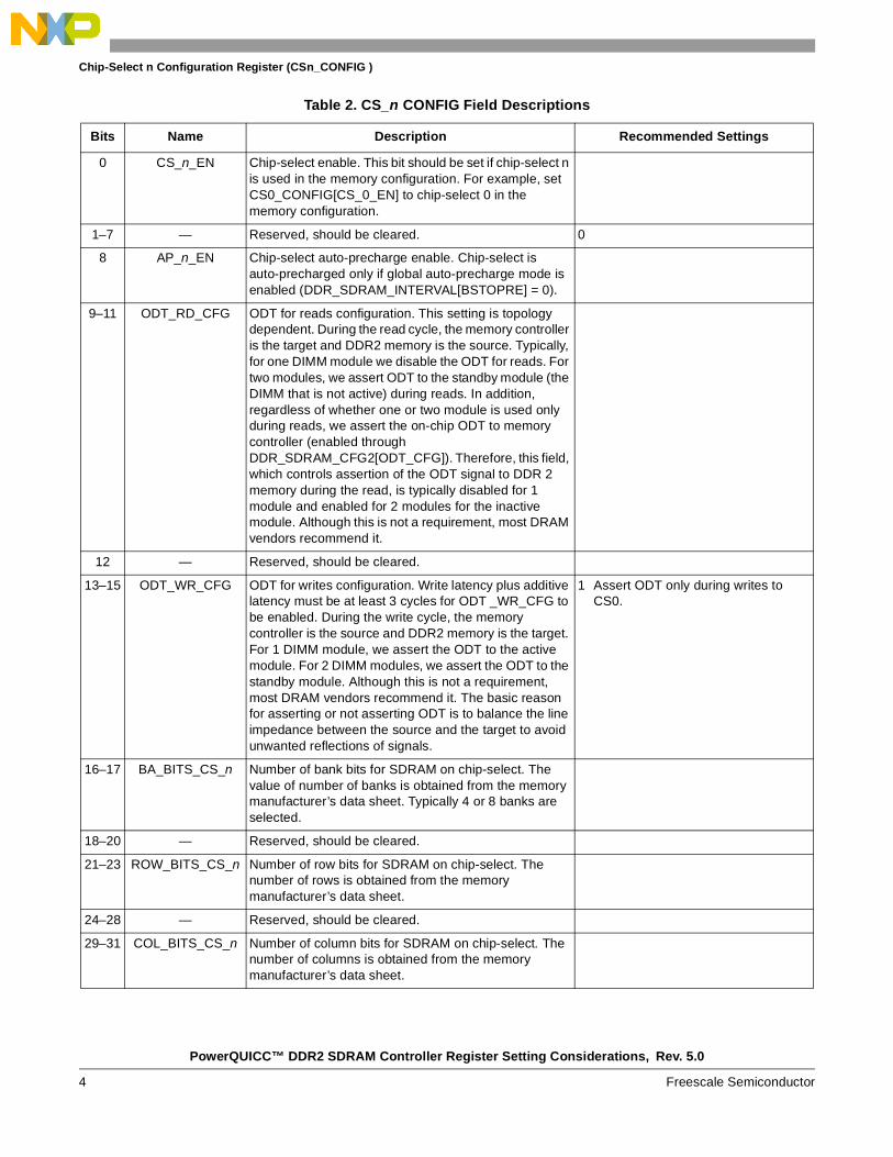
3 Chip-Select n Configuration Register (CSn_CONFIG)CSn_CONFIG enables DDR chip-select n and sets the number of row and column bits used for chip-select.
Table 1. Summary of Register Settings
Register Name Register Mnemonic Offset
1 Chip-select n memory bounds register CSn_BOUNDS 0x000
2 Chip-select n configuration register CSn_CONFIG 0x080
3 DDR SDRAM timing configuration register 0 TIMING_CFG_0 0x104
4 DDR SDRAM timing configuration register 1 TIMING_CFG_1 0x108
5 DDR SDRAM timing configuration register 3 EXT_REFREC field TIMING_CFG_3[EXT_REFREC] 0x100
6 DDR SDRAM timing configuration register 2 TIMING_CFG_2 0x10C
7 DDR SDRAM control configuration register 1 DDR_SDRAM_CFG_1 0x110
8 DDR SDRAM control configuration register 2 DDR_SDRAM_CFG_2 0x114
9 DDR SDRAM mode configuration register DDR_SDRAM_MODE 0x118
10 DDR SDRAM interval configuration register DDR_SDRAM_INTERVAL 0x124
11 DDR SDRAM clock control register DDR_SDRAM_CLOCK_CNTL 0x130
Offset 0x080 Access: Read/Write
0 1 7 8 9 11 12 13 15
RCS_n _EN — AP_n_EN ODT_RD_CFG — ODT_WR_CFG
W
16 17 18 20 21 23 24 28 29 31
RBA_BITS_CS_n — ROW_BITS_CS_n — COL_BITS_CS_n
W
Figure 1. Chip-Select Configuration Register (CSn_CONFIG)
PowerQUICC™ DDR2 SDRAM Controller Register Setting Considerations, Rev. 5.0
4 Freescale Semiconductor
Chip-Select n Configuration Register (CSn_CONFIG )
Table 2. CS_n CONFIG Field Descriptions
Bits Name Description Recommended Settings
0 CS_n_EN Chip-select enable. This bit should be set if chip-select n is used in the memory configuration. For example, set CS0_CONFIG[CS_0_EN] to chip-select 0 in the memory configuration.
1–7 — Reserved, should be cleared. 0
8 AP_n_EN Chip-select auto-precharge enable. Chip-select is auto-precharged only if global auto-precharge mode is enabled (DDR_SDRAM_INTERVAL[BSTOPRE] = 0).
9–11 ODT_RD_CFG ODT for reads configuration. This setting is topology dependent. During the read cycle, the memory controller is the target and DDR2 memory is the source. Typically, for one DIMM module we disable the ODT for reads. For two modules, we assert ODT to the standby module (the DIMM that is not active) during reads. In addition, regardless of whether one or two module is used only during reads, we assert the on-chip ODT to memory controller (enabled through DDR_SDRAM_CFG2[ODT_CFG]). Therefore, this field, which controls assertion of the ODT signal to DDR 2 memory during the read, is typically disabled for 1 module and enabled for 2 modules for the inactive module. Although this is not a requirement, most DRAM vendors recommend it.
12 — Reserved, should be cleared.
13–15 ODT_WR_CFG ODT for writes configuration. Write latency plus additive latency must be at least 3 cycles for ODT _WR_CFG to be enabled. During the write cycle, the memory controller is the source and DDR2 memory is the target. For 1 DIMM module, we assert the ODT to the active module. For 2 DIMM modules, we assert the ODT to the standby module. Although this is not a requirement, most DRAM vendors recommend it. The basic reason for asserting or not asserting ODT is to balance the line impedance between the source and the target to avoid unwanted reflections of signals.
1 Assert ODT only during writes to CS0.
16–17 BA_BITS_CS_n Number of bank bits for SDRAM on chip-select. The value of number of banks is obtained from the memory manufacturer’s data sheet. Typically 4 or 8 banks are selected.
18–20 — Reserved, should be cleared.
21–23 ROW_BITS_CS_n Number of row bits for SDRAM on chip-select. The number of rows is obtained from the memory manufacturer’s data sheet.
24–28 — Reserved, should be cleared.
29–31 COL_BITS_CS_n Number of column bits for SDRAM on chip-select. The number of columns is obtained from the memory manufacturer’s data sheet.
PowerQUICC™ DDR2 SDRAM Controller Register Setting Considerations, Rev. 5.0
Freescale Semiconductor 5
DDR SDRAM Timing Configuration 0 Register (TIMING_CFG_0)
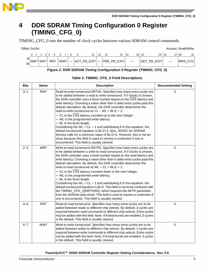
4 DDR SDRAM Timing Configuration 0 Register (TIMING_CFG_0)
TIMING_CFG_0 sets the number of clock cycles between various SDRAM control commands.
Offset 0x104 Access: Read/Write
0 1 2 3 4 5 6 7 8 9 11 12 13 15 16 19 20 23 24 27 28 31
RRWT WRT RRT WWT — ACT_PD_EXIT — PRE_PD_EXIT — ODT_PD_EXIT — MRS_CYC
W
Figure 2. DDR SDRAM Timing Configuration 0 Register (TIMING_CFG_0)
Table 3. TIMING_CFG_0 Field Descriptions
Bits Name Description Recommended Setting
0–1 RWT Read-to-write turnaround (tRTW). Specifies how many extra cycles are to be added between a read to write turnaround. If 0 clocks is chosen, the DDR controller uses a fixed number based on the CAS latency and write latency. Choosing a value other than 0 adds extra cycles past this default calculation. By default, the DDR controller determines the read-to-write turnaround as CL – WL + BL/2 + 2:
• CL is the CAS latency rounded up to the next integer. • WL is the programmed write latency. • BL is the burst length. Considering the WL = CL – 1 and substituting it in the equation, the default turnaround equation is BL/2+3. Also, JEDEC for SDRAM devices calls for a minimum value of BL/2+2. However, this is not an issue because this field is used to resolve a contention if one is encountered. This field is usually cleared.
0
2–3 WRT Write-to-read turnaround (tWTR). Specifies how many extra cycles are to be added between a write-to-read turnaround. If 0 clocks is chosen, the DDR controller uses a fixed number based on the read latency and write latency. Choosing a value other than 0 adds extra cycles past this default calculation. By default, the DDR controller determines the write-to-read turnaround as WL – CL + BL/2 + 1:
• CL is the CAS latency rounded down to the next integer. • WL is the programmed write latency. • BL is the burst length. Considering the WL = CL – 1 and substituting it in the equation, the default turnaround equation is BL/2. This field is not to be confused with the TIMING_CFG_1[WRTORD], which requires the tWTR parameter from the SDRAM data sheet. This field is used to resolve a contention if one is encountered. This field is usually cleared.
0
4–5 RRT Read-to-read turnaround. Specifies how many extra cycles are to be added between reads to different chip selects. By default, 3 cycles are required between read commands to different chip selects. Extra cycles may be added with this field. Note: If 8-beat bursts are enabled, 5 cycles is the default. This field is usually cleared.
0
6–7 WWT Write-to-write turnaround. Specifies how many extra cycles are to be added between writes to different chip selects. By default, 2 cycles are required between write commands to different chip selects. Extra cycles can be added with this field. Note: If 8-beat bursts are enabled, 4 cycles is the default. This field is usually cleared.
0

PowerQUICC™ DDR2 SDRAM Controller Register Setting Considerations, Rev. 5.0
6 Freescale Semiconductor
DDR SDRAM Timing Configuration 1 Register (TIMING_CFG_1)
5 DDR SDRAM Timing Configuration 1 Register (TIMING_CFG_1)
TIMING_CFG_1 sets the number of clock cycles between various SDRAM control commands.
8 — Reserved, should be cleared. 0
9–11 ACT_PD_EXIT Active powerdown exit timing (tXARD and tXARDS). Depending on the selection of fast exit or slow exit power-down mode in the mode register of the DDR memory, this field should be configured to tXRAD for a fast power-down and tXRADS for a slow power-down. The values can be obtained from the manufacturer’s data sheet. For details, see the next section. The fast exit mode shows a performance gain when the memory system comes out of power-down. The slow exit can save on power consumption. When memory is not put into sleep, performance is not a concern. Therefore, power saving is more meaningful. Hence If ((DDR_SDRAM_MODE[exit_active_powerdown] == fast) AND (DDR_SDRAM_CFG[DYN_PWR] == enabled))
THEN TIMING_CFG_0[ACT_PD_Exit] = tXARD
OR
If ((DDR_SDRAM_MODE[exit_active_powerdown] == slow) AND
(DDR_SDRAM_CFG[DYN_PWR] == enabled))
THEN TIMING_CFG_0[ACT_PD_Exit] = tXARDS
From manufacturer’s data sheet
12 — Reserved, should be cleared.
13–15 PRE_PD_EXIT Precharge powerdown exit timing (tXP). Should be based on tXP. From manufacturer’s data sheet
16–19 — Reserved, should be cleared.
20–23 ODT_PD_EXIT ODT powerdown exit timing (tAXPD). Should be based on tAXPAD. From manufacturer’s data sheet
24–27 — Reserved, should be cleared.
28–31 MRS_CYC Mode register set cycle time (tMRD). Should be based on tMRD. From manufacturer’s data sheet
Offset 0x108 Access: Read/Write
0 1 3 4 7 8 9 11 12 15 16 19 20 21 23 24 25 27 28 29 31
R— PRETOACT ACTTOPRE — ACTTORW CASLAT REFREC — WRREC — ACTTOACT — WRTORD
W
Figure 3. DDR SDRAM Timing Configuration 1 Register (TIMING_CFG_1)
Table 3. TIMING_CFG_0 Field Descriptions (continued)
Bits Name Description Recommended Setting

PowerQUICC™ DDR2 SDRAM Controller Register Setting Considerations, Rev. 5.0
Freescale Semiconductor 7
DDR SDRAM Timing Configuration 1 Register (TIMING_CFG_1)
Table 4. TIMING_CFG_1 Field Descriptions
Bits Name Description Recommended Setting
0 — Reserved, should be cleared.
1–3 PRETOACT Precharge-to-activate interval (tRP). Should be based on tRP. Using the min from the specification yields the best possible performance.
From manufacturer’s data sheet
4–7 ACTTOPRE Activate to precharge interval (tRAS). Should be based on tRAS. From manufacturer’s data sheet
8 — Reserved, should be cleared.
9–11 ACTTORW Activate to read/write interval for SDRAM (tRCD). Should be based on tRRD.
From manufacturer’s data sheet
12–15 CASLAT MCAS latency from READ command. Should be based on the corresponding CL value, which can be obtained from the manufacturer’s data sheet depending on the operation frequency. When the value of CL is 3 or less or if more than one choice is available, the following should be considered to make the proper selection. In Power QUICC devices the WL (Write Latency) is obtained by subtracting one from CL (WL=CL–1) which is slightly different from the conventional definition of the write latency (WL = RL–1). In addition, if ODT is used, the WL + AL (additive latency) must be at least 3 clocks, and the RL=CL + AL must be at least 3 clocks. Therefore, when the selected CL value is equal to or less than 3 and ODT is used, the AL value must be used so that RL = CL + AL must be at least 3 clocks. The CAS value selected here should be identical to the value in the corresponding field in the DDR_SDRAM_MODE[SDMODE] field.
From manufacturer’s data sheet
16–19 REFREC Refresh recovery time (tRFC). Should be based on tRFC. If the tRFC value obtained from the SDRAM data sheet is larger than the max value provided by this field, the EXTREFREC[EXTREFREC] field should be used to accommodate the difference.
From manufacturer’s data sheet
20 — Reserved, should be cleared.
21–23 WRREC Last data to precharge minimum interval (tWR). Should be based on tWR. The WR value selected here should be identical to the value in the corresponding field in the DDR_SDRAM_MODE[SDMODE] field.
From manufacturer’s data sheet
24 — Reserved, should be cleared.
25–27 ACTTOACT Activate-to-activate interval (tRRD). Should be based on tRRD. The minimum value for this field is 2 clock cycles. Therefore, if the data sheet min value is 1 clock, give this field a value of 2 clock cycles.
From manufacturer’s data sheet
28 — Reserved, should be cleared.
29–31 WRTORD Last write data pair to read command issue interval (tWTR). Should be based on tWTR. The minimum value for this field is 2 clock cycles. Therefore, if the data sheet min value is 1 clock, give this field a value of 2 clock cycles.
From manufacturer’s data sheet

PowerQUICC™ DDR2 SDRAM Controller Register Setting Considerations, Rev. 5.0
8 Freescale Semiconductor
TIMING_CONFIG_3[EXT_REFREC]
6 TIMING_CONFIG_3[EXT_REFREC] The value in the extended refresh recovery time (EXT_REFREC) field is added to the refresh recovery time when the maximum value in the Refresh recovery time field is less than tRFC obtained from the manufacturer’s datasheet.
7 DDR SDRAM Timing Configuration 2 Register (TIMING_CFG_2)
Offset 0x10C Access: Read/Write
0 1 3 4 8 9 10 12 13 15 16 18 19 21 22 23 25 26 31
R— ADD_LAT CPO — WR_LAT — RD_TO_PRE WR_DATA_DELAY — CKE_PLS FOUR_ACT
W
Figure 4. DDR SDRAM Timing Configuration 2 Register (TIMING_CFG_2)
Table 5. TIMING_CFG_2 Field Descriptions
Bits Name Description Recommended Setting
0 — Reserved, should be cleared. —
1–3 ADD_LAT Additive latency. RL = CL + AL and WL = CL -1, but WL+AL should be a minimum of 3 cycles for the ODT to be asserted correctly. Therefore, if the value of CL = <3, the AL should be at least (AL = 3–WL) to provide the minimum of 3 cycles. For example, if CAS = 3, AL should be at least equal to one (AL = 1). In addition, the additive latency should be less than the tRCD (ACTTORW) value. The AL value selected here should be identical to the value in the corresponding field in the DDR_SDRAM_MODE[ESDMODE] field.
—
4–8 CPO MCAS-to-preamble override. As stated in the reference manual, the CPO value defines the number of DRAM cycles between the time when the controller issues a read command and when the corresponding DQS preamble is valid for the memory controller. CPO is a timing calculation that starts when a read command is issued from the controller and ends when the corresponding strobe from the DDR memory is expected to be received back and recognized in the memory controller. The CPO value has memory controller, SDRAM memory, and printed circuit board (PCB) dependencies with a minimum and maximum value. Therefore, the min and max values result in an acceptable window of operation where the CPO value is valid. The CPO value is obtained from this window of operation. Therefore, if the window operation allows it, several values can be operational and the center value should be selected for the best option. Application note AN2583 provides a detailed explanation and calculation example that should be studied for a complete understanding of the CPO value and its calculation.
—
9 — Reserved, should be cleared. —
10–12 WR_LAT Write latency. Write latency (WL) should be set to CAS latency (CL) minus one: WL = CL–1. The WL value for this field is slightly different than the conventional WL= CL +AL -1. The AL (additive Latency) value is incorporated separately in the TIMING_CFG_2[AL] field.
—

PowerQUICC™ DDR2 SDRAM Controller Register Setting Considerations, Rev. 5.0
Freescale Semiconductor 9
DDR_SDRAM_CFG_1
8 DDR_SDRAM_CFG_1
13–15 — Reserved, should be cleared.
16–18 RD_TO_PRE Read to precharge (tRTP). Should be based on tRTP. The minimum value for this field is 2 clock cycles. Therefore, if the tRTP value from the data sheet calculates to the min value of 1 clock, give this field a value of 2 clock cycles. In addition, with a non-zero ADD_LAT value, this field takes a minimum value of ADD_LAT + tRTP cycles between read and precharge. For example, when tRTP=2 clks and clks AL=1 clk, then the value for this field should be ADD_LAT + tRTP=1+2=3clks.
From manufacturer’s data sheet
19–21 WR_DATA_DELAY Write command to write data strobe timing adjustment. This is highly dependent upon the board and the system topology. This field should be configured so that the first rising edge of MDQS (strobe) for a write operation meets the DRAM tDQSS specification. Also, this field is to ensure that during a write operation, the controller issues the strobe no earlier than 75 percent and no later than 125 percent of the rising edge of the clock. There can be 1 or 2 valid settings, and when more than one selection is valid, the center value is the best option. In many cases, ½ clock delay is the recommended value for this field. The value selected for the write data delay should closely follow the DDR_SDRAM_Clock_Ctrl [CLK_ADJUST] field value. In addition, CLK_ADJUST shifts MCK/MCK_B (clock) with respect to where the ADDR/CMD (address/command) is launched. In contrast, WR_DATA_DELAY shifts transmit DQS/DQS_B/DQ/ECC/DM with respect to where the ADDR/CMD was launched. Therefore, if WR_DATA_DELAY is not changed to match the CLK_ADJUST change, an offset is added between MCK and DQS.
22 — Reserved, should be cleared.
23–25 CKE_PLS Minimum CKE pulse width (tCKE). Should be based on tCKE. From manufacturer’s data sheet
26–31 FOUR_ACT Window for four activates (tFAW). Should be based on tFAW. From manufacturer’s data sheet
Offset 0x110 Access: Read/Write
0 1 2 3 4 5 7 8 9 10 11 12 13 14 15
RMEM_EN SREN ECC_EN RD_EN — SDRAM_TYPE — DYN_PWR DBW 8_BE NCAP —
W
16 17 23 24 25 26 27 28 29 30 31
R2T_EN BA_INTLV_CTL — x32_EN PCHB8 HSE — MEM_HALT BI
W
Figure 5. DDR SDRAM Control Configuration Register (DDR_SDRAM_CFG_1)
Table 5. TIMING_CFG_2 Field Descriptions (continued)
Bits Name Description Recommended Setting

PowerQUICC™ DDR2 SDRAM Controller Register Setting Considerations, Rev. 5.0
10 Freescale Semiconductor
DDR_SDRAM_CFG_1
Table 6. DDR_SDRAM_CFG_1 Field Descriptions
Bits Name Description
0 MEM_EN DDR SDRAM interface logic enable. Clear this bit first. After all the DDR controller registers are configured, there must be a 200 clock delay before this bit is set. This bit enables the memory controller, so all the registers must be configured and a there must be a delay to ensure that the set values are stable before normal operation is started in the controller.
1 SREN Self refresh enable. SREN must me enabled (SREN=1) for the self-refresh command to be issued. There are three ways entering the self-refresh mode, core going to sleep (by power management), Software forced (by enabling FRC_SC), or external HW interrupt (by enabling SR_IE). If SREN is disabled (SREN=0) and any of self-refresh entry modes applied, only MCKE will be negated and self-refresh command will not be issued.
2 ECC_EN ECC enable. Note that uncorrectable read errors may cause the assertion of core_fault_in, which causes the core to generate a machine check interrupt unless it is disabled (by clearing HID1[RFXE]). If RFXE is zero and this error occurs, ERR_DISABLE[MBED] must be zero and ERR_INT_EN[MBEE] and ECC_EN must be one to ensure an interrupt is generated.
0No ECC errors are reported. No ECC interrupts are generated.
1ECC is enabled.
3 RD_EN Registered enable. Memory DIMM is either registered or unbuffered. This information is obtained from the DIMM manufacturer data sheet. A registered DIMM has an additional latch operation and is used only for the dual in-line memory modules (memory sticks). Therefore, if the DIMM is not used, the memory is unbuffered. In a registered DIMM the CMD/Address signals are buffered. RD_EN informs the controller of the type of the memory so it can account for it. If a registered DIMM is used, the DDR_SDRAM_CFG[2T_EN] registered field must be cleared, which corresponds to 1T timing.
4 — Reserved, should be cleared
5–7 SDRAM_TYPE Type of SDRAM device to be used. The controller applies different processes for different types of memory. This field informs the controller of the type of memory with which it is to communicate.
8–9 — Reserved, should be cleared
10 DYN_PWR Dynamic power management mode.
0 Dynamic power management mode is disabled.1 Dynamic power management mode is enabled. If there is no ongoing memory activity, the
SDRAM CKE signal is negated.
11 — Reserved, should be cleared
12 32_BE DRAM data bus width. 0 64-bit bus is used.1 32-bit bus is used.
13 8_BE 8-beat burst enable. 0 4-beat bursts are used on the DRAM interface.1 8-beat bursts are used on the DRAM interface.Note: DDR2 (SDRAM_TYPE = 011) must use 4-beat bursts in either 32-bit or 64-bit bus mode.
14 NCAP Non-concurrent auto-precharge. Some older DDR DRAMs do not support concurrent auto precharge. If one of these older DRAM devices is used, this bit should be set. Otherwise, in most cases where concurrent auto precharge is supported, 0 should be selected.
15 — Reserved, should be cleared
PowerQUICC™ DDR2 SDRAM Controller Register Setting Considerations, Rev. 5.0
Freescale Semiconductor 11
DDR_SDRAM_CFG_1
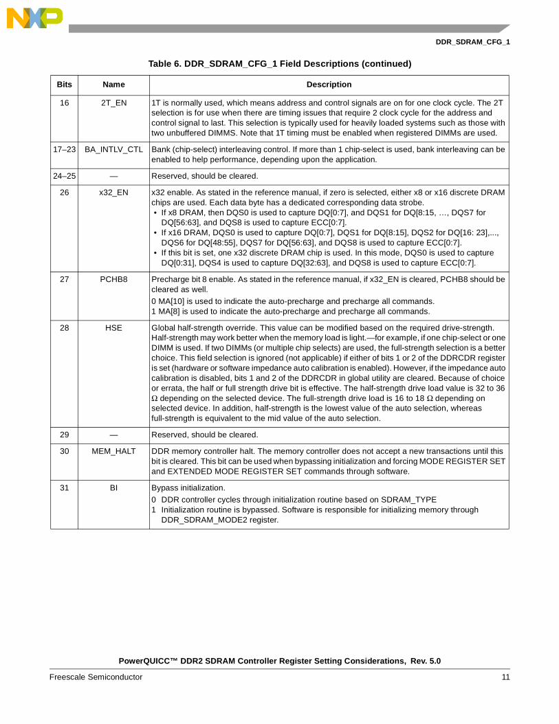
16 2T_EN 1T is normally used, which means address and control signals are on for one clock cycle. The 2T selection is for use when there are timing issues that require 2 clock cycle for the address and control signal to last. This selection is typically used for heavily loaded systems such as those with two unbuffered DIMMS. Note that 1T timing must be enabled when registered DIMMs are used.
17–23 BA_INTLV_CTL Bank (chip-select) interleaving control. If more than 1 chip-select is used, bank interleaving can be enabled to help performance, depending upon the application.
24–25 — Reserved, should be cleared.
26 x32_EN x32 enable. As stated in the reference manual, if zero is selected, either x8 or x16 discrete DRAM chips are used. Each data byte has a dedicated corresponding data strobe. • If x8 DRAM, then DQS0 is used to capture DQ[0:7], and DQS1 for DQ[8:15, …, DQS7 for
DQ[56:63], and DQS8 is used to capture ECC[0:7]. • If x16 DRAM, DQS0 is used to capture DQ[0:7], DQS1 for DQ[8:15], DQS2 for DQ[16: 23],...,
DQS6 for DQ[48:55], DQS7 for DQ[56:63], and DQS8 is used to capture ECC[0:7]. • If this bit is set, one x32 discrete DRAM chip is used. In this mode, DQS0 is used to capture
DQ[0:31], DQS4 is used to capture DQ[32:63], and DQS8 is used to capture ECC[0:7].
27 PCHB8 Precharge bit 8 enable. As stated in the reference manual, if x32_EN is cleared, PCHB8 should be cleared as well.
0 MA[10] is used to indicate the auto-precharge and precharge all commands.1 MA[8] is used to indicate the auto-precharge and precharge all commands.
28 HSE Global half-strength override. This value can be modified based on the required drive-strength. Half-strength may work better when the memory load is light.—for example, if one chip-select or one DIMM is used. If two DIMMs (or multiple chip selects) are used, the full-strength selection is a better choice. This field selection is ignored (not applicable) if either of bits 1 or 2 of the DDRCDR register is set (hardware or software impedance auto calibration is enabled). However, if the impedance auto calibration is disabled, bits 1 and 2 of the DDRCDR in global utility are cleared. Because of choice or errata, the half or full strength drive bit is effective. The half-strength drive load value is 32 to 36 Ω depending on the selected device. The full-strength drive load is 16 to 18 Ω depending on selected device. In addition, half-strength is the lowest value of the auto selection, whereas full-strength is equivalent to the mid value of the auto selection.
29 — Reserved, should be cleared.
30 MEM_HALT DDR memory controller halt. The memory controller does not accept a new transactions until this bit is cleared. This bit can be used when bypassing initialization and forcing MODE REGISTER SET and EXTENDED MODE REGISTER SET commands through software.
31 BI Bypass initialization.
0 DDR controller cycles through initialization routine based on SDRAM_TYPE1 Initialization routine is bypassed. Software is responsible for initializing memory through
DDR_SDRAM_MODE2 register.
Table 6. DDR_SDRAM_CFG_1 Field Descriptions (continued)
Bits Name Description

PowerQUICC™ DDR2 SDRAM Controller Register Setting Considerations, Rev. 5.0
12 Freescale Semiconductor
DDR_SDRAM_CFG_2
9 DDR_SDRAM_CFG_2 Offset 0x114 Access: Read/Write
0 1 2 3 4 5 6 8 9 10 11 13 14 15
RFRC_SR SR_IE DLL_RST_DIS — DQS_CFG — ODT_CFG —— VWC
W
1
16 19 20 23 24 25 26 27 28 31
RNUM_PR —— DMC — D_INIT —
W
Figure 6. DDR SDRAM Control Configuration Register 2 (DDR_SDRAM_CFG_2)
Table 7. DDR_SDRAM_CFG Field Descriptions
Bits Name DescriptionRecommended
Setting
0 FRC_SR Force self refresh. As stated in the reference manual: when this bit is cleared, the DDR controller operates in normal mode. When it is set, the DDR controller enters self-refresh mode.
1 — Reserved, should be cleared.
2 DLL_RST_DIS DLL reset disable. As stated in the reference manual: the DDR controller typically issues a DLL reset to the DRAMs when exiting self refresh. However, this function can be disabled by setting this bit during initialization. When this bit is cleared, the DDR controller issues a DLL reset to the DRAMs when exiting self refresh. When this bit is set, the DDR controller does not issue a DLL reset to the DRAMs when exiting self refresh.
3 — Reserved, should be cleared
4–5 DQS_CFG DQS configuration. The 00 value is used with DDR1 or single-ended strobe signals are used (on the controller side) with DDR2. The 0b01 value should be used with a differential strobe signal with DDR2.
6–8 — Reserved, should be cleared
9–10 ODT_CFG ODT configuration. Refers to the termination at the on-chip I/O (memory controller side). This filed should be set to assert ODT to internal IOs only during reads to DRAM. Therefore, the value of 0b10 is recommended for this field, regardless of DDR2 SDRAM topology.
0b10 is recommended.
11–15 — Reserved, should be cleared
PowerQUICC™ DDR2 SDRAM Controller Register Setting Considerations, Rev. 5.0
Freescale Semiconductor 13
DDR_SDRAM_MODE (Big-Endian Convention)
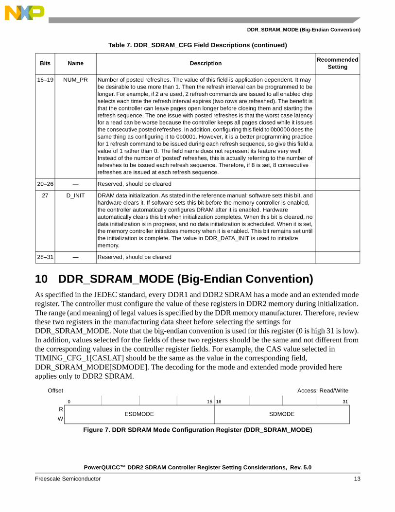
10 DDR_SDRAM_MODE (Big-Endian Convention)As specified in the JEDEC standard, every DDR1 and DDR2 SDRAM has a mode and an extended mode register. The controller must configure the value of these registers in DDR2 memory during initialization. The range (and meaning) of legal values is specified by the DDR memory manufacturer. Therefore, review these two registers in the manufacturing data sheet before selecting the settings for DDR_SDRAM_MODE. Note that the big-endian convention is used for this register (0 is high 31 is low). In addition, values selected for the fields of these two registers should be the same and not different from the corresponding values in the controller register fields. For example, the CAS value selected in TIMING_CFG_1[CASLAT] should be the same as the value in the corresponding field, DDR_SDRAM_MODE[SDMODE]. The decoding for the mode and extended mode provided here applies only to DDR2 SDRAM.
16–19 NUM_PR Number of posted refreshes. The value of this field is application dependent. It may be desirable to use more than 1. Then the refresh interval can be programmed to be longer. For example, if 2 are used, 2 refresh commands are issued to all enabled chip selects each time the refresh interval expires (two rows are refreshed). The benefit is that the controller can leave pages open longer before closing them and starting the refresh sequence. The one issue with posted refreshes is that the worst case latency for a read can be worse because the controller keeps all pages closed while it issues the consecutive posted refreshes. In addition, configuring this field to 0b0000 does the same thing as configuring it to 0b0001. However, it is a better programming practice for 1 refresh command to be issued during each refresh sequence, so give this field a value of 1 rather than 0. The field name does not represent its feature very well. Instead of the number of 'posted' refreshes, this is actually referring to the number of refreshes to be issued each refresh sequence. Therefore, if 8 is set, 8 consecutive refreshes are issued at each refresh sequence.
20–26 — Reserved, should be cleared
27 D_INIT DRAM data initialization. As stated in the reference manual: software sets this bit, and hardware clears it. If software sets this bit before the memory controller is enabled, the controller automatically configures DRAM after it is enabled. Hardware automatically clears this bit when initialization completes. When this bit is cleared, no data initialization is in progress, and no data initialization is scheduled. When it is set, the memory controller initializes memory when it is enabled. This bit remains set until the initialization is complete. The value in DDR_DATA_INIT is used to initialize memory.
28–31 — Reserved, should be cleared
Offset Access: Read/Write
0 15 16 31
RESDMODE SDMODE
W
Figure 7. DDR SDRAM Mode Configuration Register (DDR_SDRAM_MODE)
Table 7. DDR_SDRAM_CFG Field Descriptions (continued)
Bits Name DescriptionRecommended
Setting
PowerQUICC™ DDR2 SDRAM Controller Register Setting Considerations, Rev. 5.0
14 Freescale Semiconductor
DDR_SDRAM_MODE (Big-Endian Convention)
Table 8. DDR_SDRAM_MODE Field Descriptions
Bits Name Description Recommended Setting
0 ESDMODE Extended SDRAM mode. Reserved 0 Default value
1–2 ESDMODE[MRS]
The DDR controller automatically sets the MBA bits, which are used to determine which mode register is written. The values written to the extended mode register affect only the MA pins. If only 13 MA pins are available on the DRAM, then bits 0, 1, and 2 of this register affect nothing. Even though the BA bits are automatically set, one would expect reading this register to provide the same data that was originally written to it.
01 Select the extended mode register, default
3 ESDMODE[OUT]
Enable the outputs. 0 Default value
4 ESDMODE[RDQS]
This bit should be cleared. Our controller does not support RDQS. 0 Disable the RDQS
5 ESDMODE[DQS]
We typically use differential data strobes for the DDR2 memory type if the DRAM and controller offer this option. In PowerQUICC™ Pro devices, single-ended strobes are the only option, so differential data strobes should not be selected.
1 to Disable the DQS for single-ended
6–8 ESDMODE[OCD]
Software should configure this field to 0b000. The DDR controller automatically disables OCD during the initialization sequence.
000 OCD setting
9 ESDMODE[Rtt]
The DRAM termination should be set based on system topology. At higher frequencies, it may be desirable to use 75 Ω termination for the DRAM termination. However, for DDR2-400, 150 Ω termination may be sufficient. At 533 MHz, 75 Ω may be better. Also, it is not necessary to use the same Ω value as the DDR controller side. Simulation results should be a good starting-point.
01 75 Ω Rtt10 150 Ω Rtt
10–12 ESDMODE[AL]
This value should be identical to that for the SDRAM_TIMING_2[AL] for the controller setting.
posted CAS additional latency (AL)
13 ESDMODE[Rtt]
This is a continuation of bit 9. 75/150 Ω Rtt
14 ESDMODE[ODS]
Depends upon system topology and frequency. Based on your design, half strength may be a better choice. Simulation results should be a good starting-point for this setting.
0 Output drive strength of 100 percent
15 ESDMODE[DLL]
Follow the DRAM manufacturer’s recommendation on this bit. 0 Normal operations
16–18 SDMODE[MR]
Usually cleared. 0 Mode Register
19 SDMODE[PD]
If dynamic power management is used (set in DDR_SDRAM_CFG), then the DRAM disables the DRAM DLL when using slow-exit active power-down. This yields more power savings.
0 Fast PD exit (use tXRAD)
1 Slow PD exit (use tXRADS)
20–22 SDMODE[WR]
The value of this bit should be identical to that of the write recover selection. Write recover
23 SDMODE[DLL]
Zero setting is okay. The DDR controller should automatically reset the DRAM DLL during the initialization sequence.
0 Disable the DLL reset
24 SDMODE[TM]
Zero setting is okay 0 Normal mode1 Test mode
PowerQUICC™ DDR2 SDRAM Controller Register Setting Considerations, Rev. 5.0
Freescale Semiconductor 15
DDR_SDRAM_INTERVAL
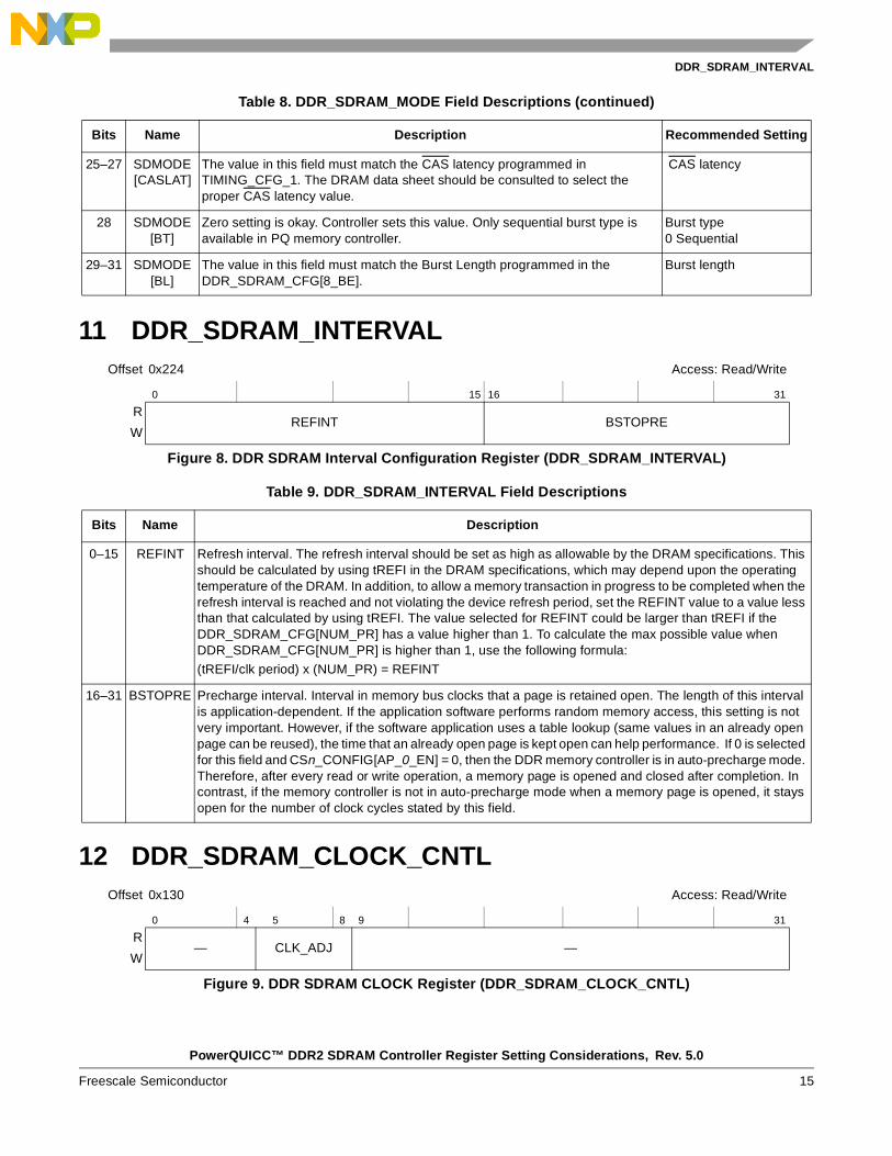
11 DDR_SDRAM_INTERVAL
12 DDR_SDRAM_CLOCK_CNTL
25–27 SDMODE[CASLAT]
The value in this field must match the CAS latency programmed in TIMING_CFG_1. The DRAM data sheet should be consulted to select the proper CAS latency value.
CAS latency
28 SDMODE[BT]
Zero setting is okay. Controller sets this value. Only sequential burst type is available in PQ memory controller.
Burst type 0 Sequential
29–31 SDMODE[BL]
The value in this field must match the Burst Length programmed in the DDR_SDRAM_CFG[8_BE].
Burst length
Offset 0x224 Access: Read/Write
0 15 16 31
RREFINT BSTOPRE
W
Figure 8. DDR SDRAM Interval Configuration Register (DDR_SDRAM_INTERVAL)
Table 9. DDR_SDRAM_INTERVAL Field Descriptions
Bits Name Description
0–15 REFINT Refresh interval. The refresh interval should be set as high as allowable by the DRAM specifications. This should be calculated by using tREFI in the DRAM specifications, which may depend upon the operating temperature of the DRAM. In addition, to allow a memory transaction in progress to be completed when the refresh interval is reached and not violating the device refresh period, set the REFINT value to a value less than that calculated by using tREFI. The value selected for REFINT could be larger than tREFI if the DDR_SDRAM_CFG[NUM_PR] has a value higher than 1. To calculate the max possible value when DDR_SDRAM_CFG[NUM_PR] is higher than 1, use the following formula:
(tREFI/clk period) x (NUM_PR) = REFINT
16–31 BSTOPRE Precharge interval. Interval in memory bus clocks that a page is retained open. The length of this interval is application-dependent. If the application software performs random memory access, this setting is not very important. However, if the software application uses a table lookup (same values in an already open page can be reused), the time that an already open page is kept open can help performance. If 0 is selected for this field and CSn_CONFIG[AP_0_EN] = 0, then the DDR memory controller is in auto-precharge mode. Therefore, after every read or write operation, a memory page is opened and closed after completion. In contrast, if the memory controller is not in auto-precharge mode when a memory page is opened, it stays open for the number of clock cycles stated by this field.
Offset 0x130 Access: Read/Write
0 4 5 8 9 31
R— CLK_ADJ —
W
Figure 9. DDR SDRAM CLOCK Register (DDR_SDRAM_CLOCK_CNTL)
Table 8. DDR_SDRAM_MODE Field Descriptions (continued)
Bits Name Description Recommended Setting

PowerQUICC™ DDR2 SDRAM Controller Register Setting Considerations, Rev. 5.0
16 Freescale Semiconductor
Revision History
13 Revision HistoryTable 11 provides a revision history for this application note.
Table 10. DDR_SDRAM_INTERVAL Field Descriptions
Bits Name Description
0–4 — Reserved, should be cleared
5–8 CLK_ADJ Clock adjustment. For lightly loaded systems (where ADDR/CMD and clock are fairly equally loaded in the system), this field is probably set to ½ DRAM cycle most of the time. This setting can be used to better center the output clock inside the ADDR/CMD valid eye at the DRAM. If the ADDR/CMD is more heavily loaded than the clock, values higher than ½ typically need to be used. For details, refer to section 4.2 in application note AN2583. In addition, note that CLK_ADJUST shifts MCK/MCK_B (clock) with respect to where the ADDR/CMD (address/command) was launched. In contrast, WR_DATA_DELAY shifts transmit DQS/DQS_B/DQ/ECC/DM with respect to where the ADDR/CMD is launched. So, if WR_DATA_DELAY is not changed to match the CLK_ADJUST change, an offset is added between MCK and DQS.
9–31 — Reserved, should be cleared
Table 11. Document Revision History
Rev.Number
Date Description
0 4/2007 Initial release.
1 6/2007 In Section 8, “DDR_SDRAM_CFG_1,” added the ECC_EN bit (Bit 2), which was omitted by mistake. In Table 6, “DDR_SDRAM_CFG_1 Field Descriptions,” on page 10, added the description of the bit.
2 8/2007 Corrected the description of Bit 26, DDR_SDRAM_CFG_1[x32_EN], in Table 6
3 10/2007 Corrected the description of bit 1, DDR_SDRAM_CFG_1[SREN], in Table 6
4 02/2008 Corrected the offset value of the DDR_SDRAM_CFG_2 register in Figure 4.
4.1 07/2008 Added further explanation for the RD_TO_PRE field values to include a non-zero ADD_LAT value in Table 5.
5.0 09/2008 In Table 8, “DDR_SDRAM_MODE Field Descriptions,” updated SDMODE[BL] description to read, “The value in this field must match the Burst Length programmed in the DDR_SDRAM_CFG[8_BE].”

PowerQUICC™ DDR2 SDRAM Controller Register Setting Considerations, Rev. 5.0
Freescale Semiconductor 17
Revision History
THIS PAGE INTENTIONALLY LEFT BLANK

PowerQUICC™ DDR2 SDRAM Controller Register Setting Considerations, Rev. 5.0
18 Freescale Semiconductor
Revision History
THIS PAGE INTENTIONALLY LEFT BLANK

PowerQUICC™ DDR2 SDRAM Controller Register Setting Considerations, Rev. 5.0
Freescale Semiconductor 19
Revision History
THIS PAGE INTENTIONALLY LEFT BLANK
Document Number: AN3369Rev. 5.009/2008
Information in this document is provided solely to enable system and software
implementers to use Freescale Semiconductor products. There are no express or
implied copyright licenses granted hereunder to design or fabricate any integrated
circuits or integrated circuits based on the information in this document.
Freescale Semiconductor reserves the right to make changes without further notice to
any products herein. Freescale Semiconductor makes no warranty, representation or
guarantee regarding the suitability of its products for any particular purpose, nor does
Freescale Semiconductor assume any liability arising out of the application or use of
any product or circuit, and specifically disclaims any and all liability, including without
limitation consequential or incidental damages. “Typical” parameters which may be
provided in Freescale Semiconductor data sheets and/or specifications can and do
vary in different applications and actual performance may vary over time. All operating
parameters, including “Typicals” must be validated for each customer application by
customer’s technical experts. Freescale Semiconductor does not convey any license
under its patent rights nor the rights of others. Freescale Semiconductor products are
not designed, intended, or authorized for use as components in systems intended for
surgical implant into the body, or other applications intended to support or sustain life,
or for any other application in which the failure of the Freescale Semiconductor product
could create a situation where personal injury or death may occur. Should Buyer
purchase or use Freescale Semiconductor products for any such unintended or
unauthorized application, Buyer shall indemnify and hold Freescale Semiconductor
and its officers, employees, subsidiaries, affiliates, and distributors harmless against all
claims, costs, damages, and expenses, and reasonable attorney fees arising out of,
directly or indirectly, any claim of personal injury or death associated with such
unintended or unauthorized use, even if such claim alleges that Freescale
Semiconductor was negligent regarding the design or manufacture of the part.
How to Reach Us:
Home Page: www.freescale.com
Web Support: http://www.freescale.com/support
USA/Europe or Locations Not Listed: Freescale Semiconductor, Inc.Technical Information Center, EL5162100 East Elliot Road Tempe, Arizona 85284 +1-800-521-6274 or+1-480-768-2130www.freescale.com/support
Europe, Middle East, and Africa:Freescale Halbleiter Deutschland GmbHTechnical Information CenterSchatzbogen 781829 Muenchen, Germany+44 1296 380 456 (English) +46 8 52200080 (English)+49 89 92103 559 (German)+33 1 69 35 48 48 (French) www.freescale.com/support
Japan: Freescale Semiconductor Japan Ltd. HeadquartersARCO Tower 15F1-8-1, Shimo-Meguro, Meguro-ku Tokyo 153-0064Japan 0120 191014 or+81 3 5437 [email protected]
Asia/Pacific: Freescale Semiconductor Hong Kong Ltd. Technical Information Center2 Dai King Street Tai Po Industrial Estate Tai Po, N.T., Hong Kong +800 2666 [email protected]
For Literature Requests Only:Freescale Semiconductor
Literature Distribution Center P.O. Box 5405Denver, Colorado 80217 +1-800 441-2447 or+1-303-675-2140Fax: +1-303-675-2150LDCForFreescaleSemiconductor
@hibbertgroup.com
Freescale™ and the Freescale logo are trademarks of Freescale Semiconductor, Inc. The Power Architecture and Power.org word marks and the Power and Power.org logos and related marks are trademarks and service marks licensed by Power.org. All other product or service names are the property of their respective owners.
© Freescale Semiconductor, Inc., 2008. Printed in the United States of America. All rights reserved.