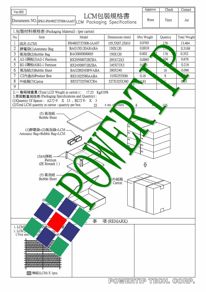
powertip ph480272t006-iaa07 tft-display distributed by ... · 16 d3 data bus. 17 d4 data bus. ......
TRANSCRIPT

PH480272T006-IAA07
4.3” TFT - 480x272 - RGB
Version: 1.0Date: 17.07.2018
Note: This specification is subject to change without prior notice
SPECIFICATION
w w w . d a t a - m o d u l . c o m

TECH. CORP.
SPECIFICATIONS
CUSTOMER : PTC
SAMPLE CODE : SH480272T006-IAA07
MASS PRODUCTION CODE : PH480272T006-IAA07
SAMPLE VERSION : 01
SPECIFICATIONS EDITION : 001
DRAWING NO. (Ver.) : JLMD- PH480272T006-IAA07_001
PACKAGING NO. (Ver.) : JPKG- PH480272T006-IAA07_001
Customer Approved
Date:
Approved Checked Designer
閆偉 劉進 陳璐
□ Preliminary specification for design input
■ Specification for sample approval
POWERTIP TECH. CORP. Headquarters: No.8, 6th Road, Taichung Industrial Park,
Taichung, Taiwan
台中市 407 工業區六路 8 號
TEL: 886-4-2355-8168
FAX: 886-4-2355-8166
E-mail: [email protected]
Http://www.powertip.com.tw
NO.PT-A-005-8

PH480272T006-IAA07 Page2 SAMPLE Ver.01
SPEC Edi.001
History of Version
Date (mm / dd / yyyy) Ver. Edi. Description Page Design by
07/11/2018 01 001 New Sample - 陳璐
Total: 28 Pages
PH480272T006-IAA07 Page3 SAMPLE Ver.01
SPEC Edi.001
Contents
1. SPECIFICATIONS 1.1 Features 1.2 Mechanical Specifications 1.3 Absolute Maximum Ratings 1.4 DC Electrical Characteristics 1.5 Optical Characteristics 1.6 Backlight Characteristics
2. MODULE STRUCTURE 2.1 Counter Drawing 2.2 Interface Pin Description 2.3 Timing Characteristics
3. QUALITY ASSURANCE SYSTEM 3.1 Quality Assurance Flow Chart 3.2 Inspection Specification
4. RELIABILITY TEST 4.1 Reliability Test Condition
5. PRECAUTION RELATING PRODUCT HANDLING 5.1 Safety 5.2 Handling 5.3 Storage 5.4 Terms of Warranty
Appendix:1. LCM Drawing 2. Packaging
Note : For detailed information please refer to IC data sheet : Primacy(TFT LCD): Sitronix--ST7282-G4
(Or compatible IC )

PH480272T006-IAA07 Page4 SAMPLE Ver.01
SPEC Edi.001
1. SPECIFICATIONS 1.1 Features
Item Standard Value
Display Type 480 * 3 (RGB) * 272 Dots
LCD Type a-Si TFT , Normally white, Transmissive type
Screen size(inch) 4.3 inch
Viewing Direction 6 O’clock
Color configuration RGB-Strip
Interface Support 16-bit Parallel interface with 8080 or 6800 series MCU
Other(controller/driver IC) ST7282-G4
(Or Compatible IC )
ROHS
THIS PRODUCT CONFORMS THE ROHS OF PTC
Detail information please refer website :
http://www.powertip.com.tw/news.php?area_id_view=1085560481/
1.2 Mechanical Specifications
Item Standard Value Unit
Outline Dimension 105.5(W) x 67.2 (L) x 8.0(H) mm
Viewing Area 96.64(W) x 55.456 (L) mm
Active Area 95.04 (W) * 53.856 (L) mm
Note : For detailed information please refer to LCM drawing

PH480272T006-IAA07 Page5 SAMPLE Ver.01
SPEC Edi.001
1.3 Absolute Maximum Ratings
Module
Item Symbol Condition Min. Max. Unit
System Power Supply Voltage VDDIO GND=0 -0.3 4.6 V
Operating Temperature TOP - -20 70 °C
Storage Temperature TST - -30 80 °C
1.4 DC Electrical Characteristics
Module GND = 0V, Ta = 25°C
Item Symbol Condition Min. Typ. Max. Unit
Power Supply Voltage
VDDIO - 3.0 3.3 3.6 V
VGH - 13 15 17.5 V
VGL - -11.5 -10 -7 V
Input H/L Level Voltage VIH - 0.7 VDDIO - VDDIO V
VIL - 0 - 0.3 VDDIO V
Output H/L Level
Voltage
VOH - VDDIO-0.4 - VDDIO V
VOL - 0 - GND+0.4 V
Supply Current IDD VDDIO = 3.3 V - 250 400 mA

PH480272T006-IAA07 Page6 SAMPLE Ver.01
SPEC Edi.001
1.5 Optical Characteristics TFT LCD Module VDDIO= 3.3 V, Ta=25°C
Item Symbol Condition Min. Typ. Max. unit -
Response time Tr+Tf 25℃ - - 30 45 ms -
Viewing angle
Top θY+
CR ≥ 10
- 60 -
Deg. Note 4Bottom θY- - 60 -
Left θX- - 60 -
Right θX+ - 60 -
Contrast ratio CR
IF= 20mA
500 600 - - Note 3
Color of CIE
Coordinate
(B/L & LCD)
White X 0.26 0.31 0.36
- Note1
Y 0.29 0.34 0.39
Red X 0.55 0.60 0.65
Y 0.29 0.34 0.39
Green X 0.29 0.34 0.39
Y 0.57 0.62 0.67
Blue X 0.10 0.15 0.20
Y 0.06 0.11 0.16
Average Brightness
Pattern=white display
(B/L & LCD)*1
IV IF= 20mA 300 400 - cd/m2 Note1
Uniformity
(B/L & LCD)*2 △B - 70 - - % Note1

PH480272T006-IAA07 Page7 SAMPLE Ver.01
SPEC Edi.001
Note 1:
*1:△B=B(min) / B(max) * 100%
*2:Measurement Condition for Optical Characteristics:
a:Environment: 25 ±℃ 5℃ / 60±20%R.H,no wind,dark room below 10 Lux at typical lamp
current and typical operating frequency.
b:Measurement Distance: 500 ± 50 ㎜ ,(θ= 0°)
c:Equipment: TOPCON BM-7 fast,(field 1°),after 10 minutes operation.
d:The uncertainty of the C.I.E coordinate measurement ±0.01,Average Brightness ± 4%
To be measured at the center area of panel with a viewing cone of 1 by Topcon
luminance meter BM-7, after 10 minutes operation (module)
Note2: Definition of response time:
The output signals of photo detector are measured when the input signals are changed
from “black” to “white”(falling time) and from “white” to “black”(rising time), respectively.
The response time is defined as the time interval between the 10% and 90% of
Amplitudes.
Refer to figure as below:
Normally White
1 2 3
6 5 4
7 8 9
VIEW AREA
LCM
θθ
Colorimeter=BM-7 fast
500 ㎜
100%90%
10%0%
Signal (Relative value)
"Black"
Tr Tf
"White" "White"

PH480272T006-IAA07 Page8 SAMPLE Ver.01
SPEC Edi.001
Normally Black
Note3: Definition of contrast ratio:
Contrast ratio is calculated with the following formula
Photo detector output when LCD is at “White” state
Contrast ratio (CR) =
Photo detector output when LCD is at “Black” state
Note4: Definition of viewing angle:
Refer to figure as below:
θ X - = 90 °
θ Y - = 90 °
X -
Y -
θ Y + = 90 °
θ X + = 90 °
X +
θ Y - θ Y +
θ X -θ X +
Y +
θ X = θ Y = 0°
Φ
Φ = 0 °6 H
Φ = 270 °
Φ = 90 °
Φ = 180 °12H
100%90%
10%0%
Signal (R
elative value)
"Black"
Tr Tf
"White""Black"
PH480272T006-IAA07 Page9 SAMPLE Ver.01
SPEC Edi.001
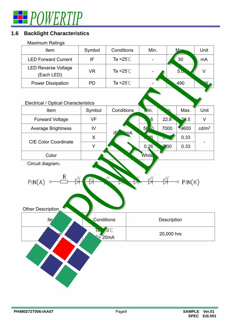
1.6 Backlight Characteristics
Maximum Ratings
Item Symbol Conditions Min. Max. Unit
LED Forward Current IF Ta =25℃ - 30 mA
LED Reverse Voltage
(Each LED) VR Ta =25℃ - 5.0 V
Power Dissipation PD Ta =25℃ - 490 mW
Electrical / Optical Characteristics
Item Symbol Conditions Min. Typ. Max. Unit
Forward Voltage VF
IF=20mA
19.6 22.8 24.5 V
Average Brightness IV 5600 7000 9600 cd/m2
CIE Color Coordinate X 0.26 0.30 0.33
- Y 0.26 0.30 0.33
Color White
Circuit diagram:
Other Description
Item Conditions Description
Life Time Ta =25℃
IF= 20mA 20,000 hrs

PH480272T006-IAA07 Page10 SAMPLE Ver.01
SPEC Edi.001
2. MODULE STRUCTURE
2.1 Counter Drawing
2.1.1 LCM Mechanical Diagram
* See Appendix
2.1.2 Block Diagram

PH480272T006-IAA07 Page11 SAMPLE Ver.01
SPEC Edi.001
2.2 Interface Pin Description
Pin No. Symbol Function
1 NC Not Connect
2 NC Not Connect
3 VSS Ground
4 VSS Ground
5 VDDIO Power Supply Voltage.
6 VDDIO Power Supply Voltage.
7 CONF
MCU interface configuration
0: 6800 Interface
1: 8080 Interface
8 RESET Master synchronize reset.
9 CS Chip select.
10 D/C Data/Command select.
11 E (RD) 6800 mode: E (enable signal)
8080 mode: RD (read strobe signal)
12 R/W (W/R)
6800 mode: R/W
0: Write cycle
1: Read cycle
8080 mode: WR (write strobe signal)
13 D0 Data bus.
14 D1 Data bus.
15 D2 Data bus.
16 D3 Data bus.
17 D4 Data bus.
18 D5 Data bus.
19 D6 Data bus.
20 D7 Data bus.
21 D8 Data bus.
22 D9 Data bus.
23 D10 Data bus.

PH480272T006-IAA07 Page12 SAMPLE Ver.01
SPEC Edi.001
Pin No. Symbol Function
24 D11 Data bus.
25 D12 Data bus.
26 D13 Data bus.
27 D14 Data bus.
28 D15 Data bus.
29 NC Not Connect
30 NC Not Connect
31 NC Not Connect
32 NC Not Connect
33 NC Not Connect
34 NC Not Connect
35 NC Not Connect
36 NC Not Connect
37 NC Not Connect
38 NC Not Connect
39 NC Not Connect
40 NC Not Connect

PH480272T006-IAA07 Page13 SAMPLE Ver.01
SPEC Edi.001
2.2.1 Refer Initial Code
LCD_WR_REG(0xe2);
LCD_WR_DATA(PLL_N-1);
LCD_WR_DATA(PLL_M-1);
LCD_WR_DATA(0x54);
LCD_WR_REG(0xe0);
LCD_WR_DATA(0x01);
delay_ms(10);
LCD_WR_REG(0xe0);
LCD_WR_DATA(0x03);
LCD_WR_REG(0xe6);
LCD_WR_DATA(count_freq(VSYNC)>>16);
LCD_WR_DATA(count_freq(VSYNC)>>8);
LCD_WR_DATA(count_freq(VSYNC));
LCD_WR_REG(0xb0);
LCD_WR_DATA(0x28);
LCD_WR_DATA(0x00);
LCD_WR_DATA((lcddev.width-1)>>8);
LCD_WR_DATA((lcddev.width-1));
LCD_WR_DATA((lcddev.height-1)>>8);
LCD_WR_DATA((lcddev.height-1));
LCD_WR_DATA(0x2d);
LCD_WR_REG(0xb4);
LCD_WR_DATA((HT-1)>>8);
LCD_WR_DATA((HT-1));
LCD_WR_DATA(0x00);
LCD_WR_DATA(HPS);
LCD_WR_DATA(HPW-1);
LCD_WR_DATA(0x00);
LCD_WR_DATA(0x00);
LCD_WR_DATA(0x00);

PH480272T006-IAA07 Page14 SAMPLE Ver.01
SPEC Edi.001
LCD_WR_REG(0xb6);
LCD_WR_DATA((VT-1)>>8);
LCD_WR_DATA((VT-1));
LCD_WR_DATA(0x00);
LCD_WR_DATA(VPS); //VPS 不需要減 1
LCD_WR_DATA(VPW-1);
LCD_WR_DATA(0x00);
LCD_WR_DATA(0x00);
LCD_WR_REG(0x11);
LCD_WR_REG(0x20);
LCD_WR_REG(0x36);
LCD_WR_DATA(0x00);
LCD_WR_REG(0x3a);
LCD_WR_DATA(0x70);
LCD_WR_REG(0x2a);
LCD_WR_DATA(0x00);
LCD_WR_DATA(0x00);
LCD_WR_DATA((lcddev.width-1)>>8);
LCD_WR_DATA((lcddev.width-1));
LCD_WR_REG(0x2b);
LCD_WR_DATA(0x00);
LCD_WR_DATA(0x00);
LCD_WR_DATA((lcddev.height-1)>>8);
LCD_WR_DATA((lcddev.height-1));
LCD_WR_REG(0xbe); //Set PWM frequence and duty
LCD_WR_DATA(PLL/65536/PWMF);
LCD_WR_DATA(256*PWM);
LCD_WR_DATA(0x01); //Set PWM by host
LCD_WR_DATA(0x10);
LCD_WR_DATA(0x10);
LCD_WR_DATA(0x00);
LCD_WR_REG(0x29);

PH480272T006-IAA07 Page15 SAMPLE Ver.01
SPEC Edi.001
2.3 Timing Characteristics
2.3.1 8080 Mode 8080 Mode Timing
8080 Mode Timing Diagram

PH480272T006-IAA07 Page16 SAMPLE Ver.01
SPEC Edi.001
2.3.2 6800 Mode 6800 Mode Timing
6800 Mode Timing Diagram (Use CS# as Clock)
6800 Mode Timing Diagram (Use E as Clock)

PH480272T006-IAA07 Page17 SAMPLE Ver.01
SPEC Edi.001
3. QUALITY ASSURANCE SYSTEM
3.1 Quality Assurance Flow Chart
Item Customer Sales R&D Q.A Manufactu
ring
Product
control Purchase
Inventory
control
Marketing
&
Design
Sample
Approval
Pilot
Run
&
Mass
Product
Ship
Out
OK
Request
Info Survey
Inquiry Project evaluation
Project Validation
Quote OK
NG
Contract
Design check
Sample test
Verification
Sample approval
NG
NG
Pilot run & Reliability test
Verification
Specification preparation OK
Mass production
Inspection NGOK
Shipment
NG
Ship out
OK

PH480272T006-IAA07 Page18 SAMPLE Ver.01
SPEC Edi.001
Item Customer Sales R&D Q.A Manufact
uring
Product
control Purchase
Inventory
control
Sales
Service
Q.A
Activity
1. ISO 9001 Maintenance Activities 2. Process improvement proposal 3. Equipment calibration 4. Education And Training Activities 5. Standardization Management
Info Claim
Failure analysis
Corrective action
Tracking
Analysis report

PH480272T006-IAA07 Page19 SAMPLE Ver.01
SPEC Edi.001
3.2. Inspection Specification ◆Scope:The document shall be applied to TFT-LCD Module for 3.5〞~15〞(Ver.B01).
◆Inspection Standard:MIL-STD-105E Table Normal Inspection Single Sampling Level Ⅱ.
◆Equipment:Gauge、MIL-STD、Powertip Tester、Sample
◆Defect Level:Major Defect AQL: 0.4 ; Minor Defect AQL: 1.5
◆OUT Going Defect Level:Sampling.
◆Standard of the product appearance test:
a. Manner of appearance test:
(1). The test best be under 20W×2 fluorescent light,and distance of view must be at 30 cm.
(2). The test direction is base on about around 45˚ of vertical line.
(3). Definition of area.
(4). Standard of inspection: (Unit:mm)
A area : viewing area
B area : Outside of viewing area

PH480272T006-IAA07 Page20 SAMPLE Ver.01
SPEC Edi.001
◆Specification For TFT-LCD Module 3.5〞~15〞: (Ver.B01)
NO Item Criterion Level
01 Product condition
1.1The part number is inconsistent with work order of production.
Major
1.2 Mixed product types. Major
1.3 Assembled in inverse direction. Major
02 Quantity 2.1The quantity is inconsistent with work order of production. Major
03 Outline dimension 3.1 Product dimension and structure must conform to structure
diagram. Major
04 Electrical Testing
4.1 Missing line character and icon. Major
4.2 No function or no display. Major
4.3 Display malfunction. Major
4.4 LCD viewing angle defect. Major
4.5 Current consumption exceeds product specifications. Major
4.6 Mura can not be seen through 5% ND filter. (Mura : Under the normal examination angle of view,the
picture has the non-uniform phenomenon.) Minor
05
Dot defect
(Bright dot、
Dark dot)
On -display
Item Acceptance (Q’ty)
Dot Defect
Bright Dot ≦ 4
Dark Dot ≦ 5
Joint Dot ≦ 3
Total ≦ 7
5.1 Inspection pattern:full white , full black , Red , Green and
blue screens.
5.2 It is defined as dot defect if defect area >1/2 dot.
5.3 The distance between two dot defect ≧5 mm.
5.4 Bright dot that can not be seen through 5% ND filter.
Minor

PH480272T006-IAA07 Page21 SAMPLE Ver.01
SPEC Edi.001
◆Specification For TFT-LCD Module 3.5〞~15〞: (Ver.B01)
NO Item Criterion Level
06
Black or white dot、scratch、 contamination
Round type
6.1 Round type ( Non-display or display):
Dimension (diameter:Φ) Acceptance (Q’ty) A area B area
Φ ≦ 0.25 Ignore
Ignore 0.25 < Φ ≦ 0.50 5
Φ > 0.50 0
Total 5
6.2 Line type( Non-display or display):
module size Length
(L) Width (W)
Acceptance (Q’ty)A area B area
3.5” to less 9”
--- W ≦ 0.03 Ignore
Ignore
L ≦10.0 0.03 <W ≦ 0.05 4 L ≦5.0 0.05 <W ≦ 0.10 2
--- W >0.10 As round type
Total 5
9” to 15”
--- W ≦ 0.05 Ignore
IgnoreL ≦10.0 0.05 <W ≦ 0.10 5
--- W >0.10 As round type
Total 5
Minor
07 Polarizer Bubble
Dimension (diameter:Φ) Acceptance (Q’ty) A area B area
Φ ≦ 0.25 Ignore
Ignore
0.25 < Φ ≦ 0.50 4
0.50 < Φ ≦ 0.80 1
Φ > 0.80 0
Total 5
Minor
X
Y
Φ=(x+y) / 2
W
L
Line type

PH480272T006-IAA07 Page22 SAMPLE Ver.01
SPEC Edi.001
◆Specification For TFT-LCD Module 3.5〞~15〞: (Ver.B01)
NO Item Criterion Level
08 The crack of glass
Symbols: X : The length of crack Y : The width of crack.Z : The thickness of crack W : terminal length t : The thickness of glass a : LCD side length
Minor
8.1 General glass chip:
8.1.1 Chip on panel surface and crack between panels:
X
Y
SP
【OK】
SP
【NG】
X Y Z
≦ a Crack can’t enter
viewing area ≦1/2 t
≦ a Crack can’t exceed the
half of SP width. 1/2 t < Z ≦2 t
X
YZ
YZ
XY
Z
Seal width

PH480272T006-IAA07 Page23 SAMPLE Ver.01
SPEC Edi.001
◆Specification For TFT-LCD Module 3.5〞~15〞: (Ver.B01)
NO Item Criterion Level
08 The crack of glass
Symbols: X : The length of crack Y : The width of crack. Z : The thickness of crack W : terminal length t : The thickness of glass a : LCD side length
Minor
8.1.2 Corner crack:
8.2 Protrusion over terminal:
8.2.1 Chip on electrode pad:
Z
X Y
X Y Z
Front ≦ a ≦ 1/2 W ≦ t
Back ≦ a ≦ W ≦ 1/2 t
X
Y
Z
X Y Z
≦1/5 a Crack can’t enter viewing area
Z ≦ 1/2 t
≦1/5 a Crack can’t exceed the half of SP width.
1/2 t < Z ≦ 2 t
W

PH480272T006-IAA07 Page24 SAMPLE Ver.01
SPEC Edi.001
◆Specification For TFT-LCD Module 3.5〞~15〞: (Ver.B01)
NO Item Criterion Level
08 The crack of
glass
Symbols: X : The length of crack Y : The width of crack. Z : The thickness of crack W : terminal length t : The thickness of glass a : LCD side length
Minor
8.2.2 Non-conductive portion:
⊙ If the chipped area touches the ITO terminal, over 2/3 of
the ITO must remain and be inspected according to
electrode terminal specifications.
8.2.3 Glass remain :
8.2.4 Cracking
X Y Z
≦ a ≦ 1/3 W ≦t
X Y Z
≦ 1/3 a ≦ W ≦t
Not Allowed

PH480272T006-IAA07 Page25 SAMPLE Ver.01
SPEC Edi.001
◆Specification For TFT-LCD Module 3.5〞~15〞: (Ver.B01)
NO Item Criterion Level
09 Backlight elements
9.1 Backlight can’t work normally. Major
9.2 Backlight doesn’t light or color is wrong. Major
9.3 Illumination source flickers when lit. Major
10 General
appearance
10.1 Pin type、quantity、dimension must match type in structure
diagram. Major
10.2 No short circuits in components on PCB or FPC . Major
10.3 Parts on PCB or FPC must be the same as on the
production characteristic chart .There should be no wrong
parts , missing parts or excess parts.
Major
10.4 Product packaging must the same as specified on packaging
specification sheet. Minor
10.5 The folding and peeled off in polarizer are not acceptable. Minor
10.6 The PCB or FPC between B/L assembled distance(PCB or
FPC ) is ≦1.5 mm. Minor

PH480272T006-IAA07 Page26 SAMPLE Ver.01
SPEC Edi.001
4. RELIABILITY TEST
4.1 Reliability Test Condition (Ver.B01)
NO. TEST ITEM TEST CONDITION
1 High Temperature
Storage Test Keep in +80 ±2℃ 240 hrs Surrounding temperature, then storage at normal condition 4hrs.
2 Low Temperature
Storage Test Keep in -30 ±2℃ 240 hrs Surrounding temperature, then storage at normal condition 4hrs.
3 High Temperature /
High Humidity Storage Test
Keep in +60 ℃ / 90% R.H duration for 240 hrs Surrounding temperature, then storage at normal condition 4hrs. (Excluding the polarizer)
4 Temperature Cycling
Storage Test
-30℃ → +25℃ → +80℃ → +25℃
(30mins) (5mins) (30mins) (5mins)
20 Cycle
Surrounding temperature, then storage at normal condition 4hrs.
5 ESD Test
Air Discharge:
Apply 2 KV with 5 times Discharge for each polarity +/-
Contact Discharge:
Apply 250 V with 5 times discharge for each polarity +/-
1. Temperature ambiance : 15℃~35℃ 2. Humidity relative : 30%~60% 3. Energy Storage Capacitance(Cs+Cd) : 150pF±10% 4. Discharge Resistance(Rd) : 330Ω±10% 5. Discharge, mode of operation : Single Discharge (time between successive discharges at least 1 sec)
(Tolerance if the output voltage indication : ±5%)
6 Vibration Test
(Packaged)
1. Sine wave 10~55 Hz frequency (1 min/sweep)
2. The amplitude of vibration :1.5 mm
3. Each direction (X、Y、Z) duration for 2 Hrs
7 Drop Test (Packaged)
Drop Direction :※1 corner / 3 edges / 6 sides each 1time
Packing Weight (Kg) Drop Height (cm)
0 ~ 45.4 122
45.4 ~ 90.8 76
90.8 ~ 454 61
Over 454 46

PH480272T006-IAA07 Page27 SAMPLE Ver.01
SPEC Edi.001
5. PRECAUTION RELATING PRODUCT HANDLING 5.1 SAFETY
5.1.1 If the LCD panel breaks , be careful not to get the liquid crystal to touch your skin.
5.1.2 If the liquid crystal touches your skin or clothes , please wash it off immediately by
using soap and water.
5.2 HANDLING 5.2.1 Avoid any strong mechanical shock which can break the glass.
5.2.2 Avoid static electricity which can damage the CMOS LSI—When working with the
module , be sure to ground your body and any electrical equipment you may be using.
5.2.3 Do not remove the panel or frame from the module.
5.2.4 The polarizing plate of the display is very fragile. So , please handle it very
carefully ,do not touch , push or rub the exposed polarizing with anything harder
than an HB pencil lead (glass , tweezers , etc.)
5.2.5 Do not wipe the polarizing plate with a dry cloth , as it may easily scratch the
surface of plate.
5.2.6 Do not touch the display area with bare hands , this will stain the display area.
5.2.7 Do not use ketonics solvent & aromatic solvent. Use with a soft cloth soaked with
a cleaning naphtha solvent.
5.2.8 To control temperature and time of soldering is 320±10℃and 3-5 sec.
5.2.9 To avoid liquid (include organic solvent) stained on LCM .
5.2.10 Caution!( LCM products with Capacitive Touch Panel)
Strong EMI-sources such as switch-mode power supplies (SMPS) can lead to touch
malfunction (e.g. ghost-touches).
Therefore, the touch needs to be thoroughly tested inside the target application.
5.3 STORAGE 5.3.1 Store the panel or module in a dark place where the temperature is 25℃ ±5℃
and the humidity is below 65% RH.
5.3.2 Do not place the module near organics solvents or corrosive gases.
5.3.3 Do not crush , shake , or jolt the module.
5.4 TERMS OF WARRANTY 5.4.1 Applicable warrant period
The period is within thirteen months since the date of shipping out under normal
using and storage conditions.
5.4.2 Unaccepted responsibility
This product has been manufactured to your company’s specification as a part for
use in your company’s general electronic products. It is guaranteed to perform
according to delivery specifications. For any other use apart from general
electronic equipment , we cannot take responsibility if the product is used in
nuclear power control equipment , aerospace equipment , fire and security

PH480272T006-IAA07 Page28 SAMPLE Ver.01
SPEC Edi.001
systems or any other applications in which there is a direct risk to human life
and where extremely high levels of reliability are required.

PAR
T NO
:
Page
Scale
Unit
DR
AW
ING
NAM
E :D
esign
Approve
Check
PO
WE
RTIP
TEC
HN
OLO
GY C
OR
POR
ATION
久 正
光 電
股 份
有 限
公 司
TITLE:
Material
Quantity
Surface
Thickness
AB
CD
EF
GH
123456
MM
JLMD
-PH
480272T006-IAA07
PH
480272T006-IAA07
LCD
Module D
rawing
003002001
RE
V B
YR
EV
ISE
RD
ATE
NE
W D
RA
WIN
G
-----1/1
1:1.3
Ryan
004005006007
Length(Min)
(mm
) Tolerance
PrecisionP
recision Level
Air
Terry2018/06/22
Air

A L L T E C H N O LO G I E S . A L L CO M P E T E N C I E S . O N E S P E C I A L I S T.
w w w . d a t a - m o d u l . c o m
More information and worldwide locations can be found at
DATA MODUL AG
Landsberger Straße 322 DE-80687 Munich Phone: +49-89-56017-0
DATA MODUL WEIKERSHEIM GMBH
Lindenstraße 8 DE-97990 Weikersheim Phone: +49-7934-101-0