practical electronics 2'6 inexpensive oscilloscope • · pdf fileinexpensive...
TRANSCRIPT

Practical Electronics
MARCH 1965 PRICE
4 GREAT CONSTRUCTIONAL PROJECTS
INEXPENSIVE OSCILLOSCOPE • AUTO PARKING LIGHT
DIGITAL DISPLAY CLOCK • RADIO TUNER
PfusStoOHWM
ofymMefo
WfiiCOhdvcfa
OwrtPesioh
Sf'-'- •
2'6
mm
i
c mM
■
..
mm \

VOL. 1 No. 6
MARCH 1985
GOING SHOPPING
You cannot build without bricks. The bricks of electronics —circuit components and ancillary items of hardware-
have to be purchased from somewhere. Undoubtedly some constructors will have the traditional "junk box" to dip
into, but those thousands who have only in recent limes
taken interest in electronics as a hobby will be without any
such accumulation of parts. And in any case junk boxes need replenishing and bringing up to dale from lime to lime.
The electronics constructor is particularly fortunate in
being well catered for by a large number of retailers long experienced in administrating to his needs. Some of these
businesses deal exclusively in new branded or proprietary
components, some deal exclusively in manufacturer's or government surplus components or equipment, while there
are those who handle a selection of both.
THIS MONTH
CONSTRUCTIONAL PROJECTS
ELECTRIC CLOCK WITH
DIGITAL DISPLAY 324
INEXPENSIVE OSCILLOSCOPE 328
MAGIC BOXES 336
GUITAR AMPLIFIER 343
AUTOMATIC PARKING LIGHTS 347
TWO BAND RADIO TUNER 354
SPECIAL SERIES
It is not our purpose here to advise for or against the use
of either of the above-mentioned categories of electronic
goods. This will be a matter for the individual to decide
for himself in light of a number of factors. It might be
useful, however, to explain that the term "surplus" does not necessarily mean that the components are of the used or
second-hand variety; in some instances they may be brand
new components of current type which a large manufacturer
has found to be redundant to his requirements.
There are certainly other components and pieces of equip-
ment on the market that bear unmistakable signs of having
been used. These items are usually of government or service origin and are quite often good economical propositions, even
if only part can be salvaged for re-use. However, those inexperienced in such matters arc recommended to proceed
cautiously when contemplating the purchase of such equip-
ment, and to obtain expert advice regarding the potential
utility of either the whole equipment, or its constituent
parts. The rapid changes in component design in recent years
mean that many of the parts in the older surplus equipments
are electrically or physically incompatible with those used in projects of modern design. On the other hand, to some of the
more venturesome and intrepid spirits in our fraternity this
older equipment presents a source of much enjoyment and
the opportunity for them to exercise their skill at improvisa-
tion at minimum cost.
SEMICONDUCTORS—2 339
BEGINNERS START HERE—5 352
GENERAL FEATURES
HALL EFFECT 360
DESIGN OF CERAMIC PICK-UP
CARTRIDGES 366
NEWS AND COMMENT
EDITORIAL 323
ELECTRONORAMA 350
NEW PRODUCTS 359
DETACHED PARTICLES 364
READOUT 374
Our April issue will be publ Thursday, March 11
ubllshed on
All correspondence Intended for the Editor should be addressed to; The ^1 !o^,^RA<i,1,,1 a'rtK a'l FTkcTROT^^S^Georfte^ewiics Ltd!! House. Southampton Street, London. W.C.a. Editorial and Advertisement OfBees: PRACTICAL ELECT* • s JL . R . Tower House. Southampton Street. London. JV C.2. Phone: Temple nar 436L Te.egrams: *0-^ Including postngc for one year, to any part of the world, 358. © George Sewnc* Ltd., I ■ J - slonalorv to the Berne Convention and articles published In PRACTICAL ELECTRONICS Is specially reserved throughout the countries signatory the U.S.A. Reproductions or Imitations of any of these are therefore expressly forbidden.

PERSONALLY, I usually give it up as a bad job!
Trying to see what the lime is in the middle of ihc
night, I mean. Have you tried it lately? It lakes
five minutes to sec, dimly, the remaining luminescence
on the clock face as shapeless blodgcs. Deciding
which hand is which and interpreting with a sleep-
befuddled brain their message is beyond my power of
concentration. If you switch the light on to read it
properly, the results may be twofold:
(a) Panic on the part of your wife who imagines a
major catastrophe.
(b) You can't get to sleep for hours afterwards.
As I said, I usually give it up as a bad job. What's
wanted is a clock that is easy to read at all times of
the day or night, hence illuminated digital
presentation.
Having a preference for electronic rather than
electro-optical devices, I chose digitrons for the pre-
sentation although the latter would do.
Digitrons such as Ericsson GRIOJ or Mullard
G530iVl are readily available at about 32s 6d each.
Having decided on the presentation, the next thing is to
decide on the method of time measuring to be used.
The possible schemes are:
(a) All electronic with countdown from the mains
frequency.
(b) All electronic with countdown from an internal
oscillator.
(c) Electro-mechanical synchronised with mains
frequency.
(d) Electro-mechanical with self-contained frequency
source.
Examining these possibilities, we find that:
(a) Can be devised with binary counters driven from
the mains frequency. The countdown would be
done in the following stages: 50 : I, 60 : I to
give seconds; 60 : I to give minutes; 12 : I to
give hours. Using binary division, this would
require 44 valves or semiconductors not including
coupling amplifiers or diodes. This scheme is
likely to be loo large and expensive. Tunnel
diodes have been used as reliable 30 : I count-
down devices and makes this method worth

CD MOTOR
-'/a1
Fig. la. Plan view showing the gearing mechanism and the spindle spacing dimensions
JAPPED ABA 0
MOTOR
£ (2^ i ® !
(D
S is u ^ VA y is u U VA
Fig. lb. Elevation showing details of the wafer switch mountings. It will be noticed that the gearing shown on the drawing does not resemble that in the photograph below. The gearing in the photo- graph has been modified to form a more robust mounting for the teeth
SWITCH WAFERS
investigating. Using decimal counters, such as
dekatrons (they can be obtained to count up to
12 as well as 10 using, for example, Ericsson
GCI2/4B tubes), 7 dekatrons and six coupling
amplifiers would be required.
(b) This approach was discarded because of the
accuracy required of the frequency source. A
clock accuracy of I minute per month requires
an oscillator accuracy and stability of two parts
in 10°. In addition, to reduce the countdown
circuitry, a basic frequency of 50c/s or less
would be required.
(c) This method can be achieved by using a syn-
chronous motor suitably geared to switches for
the countdown. Almost any clock motor is
suitable but one with built-in gearing to give
I r.p.m. is the best. The gearing needs to be
10 : I for unit minutes. 6 : 1 for tens of minutes
and 12 : I for hours when using a I r.p.m.
motor assembly.
(d) Can be obtained by using a velocity servo, using
a mercury standard cell for reference and for the
lacho licld supply. The other requirements
being a power amplifier and split field motor/
tacho. The gearing equipment requirements
are as in (c) if the servo gives a I r.p.m. output.
Of these schemes, (c) was selected as being the
cheapest and simplest method of the four.
G 9
V
I Ui ,5 r*v
325

•X u
_o "C
"O 0) *-» u a> c c o u
gj
J5 2
E °
rr cNra
_CJ CJ
g-g. _o _«
.. oo oo 9 .E .- ^ VI v> U .^ — fS
W)
"O « w u g-fc
oj
> v»
n3
SJ n c
? 2 o .£ fn cj .a.
_a ' o ^ Q. 4»
.? i g S. ~>-5
IA
to
<7« f*.
S5 to — o «tJ
c "2
E"2
o v E§
"C £ w o ^ C ) 0) ^ to u
III o to g;
c O v c v> k. o
"O
> ro >
v» 00 2
v» vt 3 0 O 9 X
r* o
11 .2U
z < z
o
E o t- 00 o
u
t £ o. E o
VJ
lO
VI P9 X o
VI 0)
"3 — OQ
fN s < o
3 z
(N m f 10 vo QQQQQD
o
Z ~ o lO
"O k. _rt
3 Z
O c o v> S
9 . > — 3>> >
> >
\0
_x o lO
a
r>-
r-ajoo — r^m-riovor^ rsr^fSrorororororororo ctczaLctaiaiaictctaict
PS
-h VI k. S VI vi a
a -X
a -X o lO
a -X r>
o r
CO
t to vo r--. a) o o — rs ro tt to >o rMiNfxr^rNfMr^ c£a:a:a:c£a:a:c£c£c£oic£c£
aacjaa a ^ _X -X ^ -X ^ o r-^ o r^. r^- o rs T to T to
a -X
— rc — o — rc ro
fsron-ko>or^coa*-— — — c£c£<*.c£(*LcLcLcLcLc£cLc£.

SWITCHING
The gearing from the motor is the only item that
requires further consideration. With normal gearing,
the hours switch would take 1 hour to cover one
segment and this would make the time of switch-over
unreliable. What is required is for all the switches to
change from one segment to another rapidly, i.e.
within a few seconds, but still to retain the correct gear
ratio. The gears drive the wipers of wafer switches to
switch the supplies to the numeral that it is required to
display. The gearing is shown diagrammalically in
Figs, la and b.
This will operate all switches at the same speed
giving about 5 seconds for the complete changeover
from segment to segment but less than 1 second for
numeral change.
The switch wafers required are 10-way 36°, six-way 60 '
and 12-way 30°, that is the segments must be evenly
disposed. The 12-way wafer is a standard, the six-way
is a 12-way wafer with the segments connected in pairs.
The 10-way wafer was a problem and the only
suitable wafer found was the Painton winkler switch
wafer which is a 30 contact wafer and thus the contacts
were wired in threes. All wafers must be make before
break to avoid interruptions of the display of hours and
tens of minutes.
The digitrons require +170 volts to strike and
140 volts as the minimum maintaining voltage, +60V
on a cathode will extinguish that cathode. The current
is 2mA. As filtering of the supply is unnecessary, a
simple half-wave rectified supply is used.
Earthing any cathode will produce about +60 volts
r.m.s. on all the other cathodes. The anode resistor
is included to limit the total valve current if a fault
should occur. The circuit used gives the greatest
protection to the digitron if either a short circuit or
open circuit should occur.
The full circuitry of the clock is shown in Fig. 2.
Note that rather than have a separate switch wafer
for the tens of hours, diodes are used so that the 10, 11
and 12 positions of the hours switch wafer will light the
I on the tens of hours digitron as well as the required
unit. The diodes are required to prevent the 1 and 2
positions on the hours switch from lighting the 1 on the
last digitron.
CONSTRUCTION
Details of the switching mechanism are shown in
Figs, la, b. The "teeth" of the gears are made from stout
piano wire soldered on to i in diameter discs. A
wooden jig is strongly recommended for this soldering
with the wires laid in saw cuts. Cut the wires to
length after soldering. The discs are then bolted with
4 B.A. screws to the end of i'm diameter spacers and
secured with Aralditc. The spacer is drilled out to iin
for part of its length for attaching to the switch shaft.
The switch wafer is mounted on the baseboard with its
drive shaft in the usual way. The switch detent
mechanism is however prevented from working by
either removing the ball bearings or the detent spring.
The gears must be fixed to the switch shaft in the
correct position by using grub screws. This is best
found when the wiring is complete and with the power
supply switched on. Once this is done, the clock can
be set to the correct time by rotating the gears indi-
vidually.
Well that's it. Incidentally, the clock gives almost
enough light to read the time on my watch!
o
r-e-—e—
I |—€>-—©—
■e-
h-o- -e-
H-O-—O"
H-o- ©■
f—o- "©■
R37
R36
R35
R34
R53
R32
R3t
R30
R29
R28
l"0
r-o—o- I H-O- 0—
1—e-—©—
_rr:QR27 rw
r i
R27
R25
-O—©—
r-o-—©■ i h-©—e— I H-€>-—©■ I L-o-—©—
R19
I ro-—©—
R24
R25
R22
R21
R20
O- -0-
O >■
TO R26-
R19
R18
R17
| HO
I! L-0--
ho
I HO-—0— M I H-© 0 II I HO 0—
Ir"0"
H-© 0 I Ho
Lo 0
R16
R15
R14
R13
R12
R11
R10
R9
R8
R7 I /♦-TO R7 I—O 0— R6
H-O- ©— R3
H O R2
TO R18-
—0
—0
■o
T0R6-
—©
—O 0- 01
—0 ©TRS TO WIPERS N 1 OF S1,S2,S5
TAG 10 SI
R4 1—*—
1 o o—©-i
"V— i
-O-U
^■o 0
0 07 & TAG 12,SI ^—© 0 06 & TAG 11, SI
O o o
->e -
-K 02 ->e e—-o-i
0+ 03 ->e 0-1
0"\ 04 ->e
PIN TAG 3 ' 0
4 9
5 8
6 7
7 6
9 5 VV4
10 4
11 3
12 2
13 1
2 3 ' O] 9 5
10 4
11 3
12 0/3 2
13 1
2
3 & 05
4 *
9
5
6 7
7 6
9 >-V2
10 4
H 3
12 2& 07
13 1& 06
2
PIN 2,VI
S3
^S2
SI
NEON
PIN 13,VI
NEON
PIN 3,V2&Rt7
Fig. 3. Layout of components on a piece of perforated board. This diagram is not to scale
327

i
y.
*
By
P. Cairns
PART ONE
SPECIFICATION
Display tube
Electrostatically focused and deflected, 3in
diameter screen, medium persistence green
phosphor. Type 3BPI. 3EPI. or 3GPI.
Y amplifier
Input impedance I M12, 30pF.
Maximum sensitivity approximately 200mV/cm.
Six-range attenuator with following steps:
(I) XI OdB; (2) X3 lOdB; (3) XIO 20dB;
(4) X30 30dB: (5) XI00 40dB; (6) X300 50dB.
Response iSdBfrom 5c/s to I75kc/s, with a useful
display gain up to I Mc/s.
Time base and X amplifier
Time base switch provides the following ranges:
(I) lOOms/cm to lOms/cm; (2) lOms/cm to I ms/cm;
(3) I ms/cm tdOC/is/cm; (4) IOO/«/cmto IO//s/cm.
The fine control gives adequate overlap between
ranges.
The fifth position gives facilities for external
signal input to the X amplifier while muting
time base and sync signals.
With the time base on, the X amplifier gain
gives a trace expansion of at least six times.
With the switch in the external position the
X amplifier has a maximum sensitivity of about
800mV/cm, and a response of lOc/s to 75kc/s
^SdB. and a useful display gain up to 200kc/s.
Sync
Synchronising is continuously variable for all
types of Y input signal. Switching allows an
external sync signal to be applied if required.
Calibration
An internal calibration unit gives a square wave
output at 50c/s with a mark/space ratio of I : I.
an amplitude of I volt peak to peak, and a rise
time better than 5/<s.
Power consumption
The total power consumption from the mains
is less than 50 watts.
Dimensions
The approximate overall dimensions are height
I2in. width 9in, and depth I Sin.
U The following article describes an extremely useful
and comprehensive oscilloscope which the writer
has used extensively during the past few months and
which has proved indispensable in practice and
reliable in operation. This instrument should prove
of particular interest to both the serious experimental
amateur and the spare lime radio or television service-
man. Those interested in audio equipment work
would also find it very useful.
328
The oscilloscope was designed with a number of
factors in mind. First, the circuit had to use all
standard easy-to-get components and valves, while the
cost had to be kept to a minimum. Second, the circuit
had to be kept as simple as possible for ease of
construction and be simple to set up, while maintaining
the majority of useful features met with in much more
expensive commercial instruments. Finally, it had to
have reliability over a long period together with ease

*
u-« in X u. _i P Ou.
§ ' ' 3,
rsj 'J " -
^ O *\JCS k> Q :• o: —
m
w
QliNj h-y O
rj: av
G o
ii 11 <NJ
K
=:8 M O
- a .. — «iro
o rsj O* M I I
rv. W
O »— co c;
- > <-4 ^ s CO cr- 1 — »o. -rfll
. '• \ cri m o a: k» a: k>
W—W w y • o c; ro (\.ia. f • a. O
3 in
il 5 u o <«> a O q 1 y 11 ^ O
•O > m <•> N
w w w -o C
O
<>
W -G
o t m C? m O G s ^ G (NJ OO ^ m u#
'NJ G 0=0 o o > o •N u> 2 •/
II t. ~ r.» ~,
a
IM
II O O HI O u- - > 'V TH IM
Q O o A -
M ro * • IM o in
II m
?■ H
- S Si S
QQQ_/-
-/ o k*. «J
V3 ^ o NO < = r * o
a in i
o
§ "s o
o u
■£ ■O c o
s
o u
§
>s
&
t) *
I *>
£
329

fi '4
'M m m
Underside view of the com- pleted instrument
and simplicity of servicing which meant that the
number of different types of valves employed had to he
kept to a minimum.
The circuit finally evolved after a considerable
amount of work is shown in Figs. 1, 2, and 3 and
is considered the best compromise between the various conflicting features mentioned above.
The instrument is built around a 3in tube with
green trace and relatively short persislance such as
the type 3BPI, 3EP1, or 3GP1. These are American
surplus lubes and can be obtained at very reasonable
prices although, as with all surplus equipment, the
supply position docs fluctuate from time to time and
place to place. Any of these three tubes may be
used quite satisfactorily in this instrument, the minor
differences in characteristics being automatically taken
care of during the setting up and calibration of the
completed oscilloscope.
Only two types of valves are used in the 10 valve
circuit: these are the*bheap and easily replaceable
double triodes ECC81 and ECC82.
A conventional h.t. and e.h.t. arrangement is used.
The only high tolerance components used are in the
Y attenuator and a few resistors in the Y amplifier.
PRINCIPAL FEATURES
The main design features include a six range Y
attenuator in lOdB steps to 50dB, cathode follower
input in both X and Y amplifier first stages, linear X
and Y gain controls, and push-pull d.c. coupled outputs
to the c.r.t. deflection plates. Both X and Y shift
controls are d.c. coupled giving a positive shift action
in both planes. A four range lime base circuit with a
fine control gives ample overlap between ranges.
Facilities are also available for external X input,
the time base and sync circuits being muted in this
position. The sync circuit also has switching facilities
for external or internal use while the sync control
locks the time base to the signal being displayed. The
Y amplifier was designed to give the best compromise
between gain and bandwidth in the number of stages
available. The maximum sensitivity of 200mV/cm
with a flat response to nearly 200kc/s and a useful
display gain to over IMc/s should cover the majority
of practical applications.
An internal transistor square wave calibration circuit
is included, this being extremely useful for checking
and selling up the Y amplifier. It also provides a
useful time calibration check on the time base.
Finally, a prc-set astigmatism control is used to
give optimum focus over the screen width.
- IE'. ' "• »^S. IP I
Features which are not included and which are
found in some of the more expensive commercial
oscilloscopes are: stabilised h.t. and e.h.t. supplies,
d.c. coupled Y amplifier with differential input, and
extensive triggering facilities. While these features
are obviously advantageous and increase the scope
and usefulness of an instrument, it was not considered
worthwhile to include them in the relatively simple and
practical oscilloscope envisaged. Not only would
their incorporation have increased the size and circuit
complexity of the instrument, but the extra number of
stages and power supplies to perform these functions
would have made the oscilloscope prohibitively
expensive for the amateur constructor and the
advantages derived would be outweighed by the
extra expense involved.
One other point which may be mentioned (though
in the opinion of the writer it is a debatable one) is
the inclusion of switching or plug facilities for direct
external connection to the c.r.t. deflection plates. In
practice the number of occasions when this feature
is required are extremely rare. The stray capacitance
due to the plugs or switching and the extra wiring
involved all mean extra loading on the X and Y
amplifier output stages with a resultant deterioration
at the h.f. end of the amplifier response curves. For
this reason this feature was not incorporated in the design though it could be included at negligible cost
if required, but with consequent fall off in amplifier
h.f. gain.
Before going on to the constructional details, a brief
description of the various circuit functions will be of
interest and will also help to clarify the working of
the instrument and the uses to which it may be put.
POWER SUPPLIES
Fig. I shows the power supply section, the cathode
ray tube, and the calibration unit.
The mains transformer T1 feeds the full-wave
rectifier VI, and the pulsating d.c. output is smoothed
by LI and Cl. The h.t. is at a potential of 315 volts.
Three heater windings are provided on Tl: y-y
for the c.r.t., x-x for the valves V4-V8 inclusive and
z-z for the rectifier VI. The valve heater winding
x-x is centre lapped—this is essential in order to
reduce hum in the amplifiers to a minimum.
The e.h.t. is derived from a half wave voltage
doubling circuit comprising C5, Dl, and D2. The
final output after smoothing by C6, R14, and C7, is
in the region of minus 750 volts with respect to earth.
330

As A3 is fed from the aslig. control VRI connected in
a divider network across the h.t. supply, this means
that approximately IkV is applied across the c.r.t.
The e.h.t. divider chain R15-VR3 provides the
necessary voltage levels for the tube electrodes, VR2
being the focus control and VR3 the brilliance control.
Adequate decoupling is provided against spurious signal pick-up by means of C2, C8, and C9. Flyback
suppression is applied to the tube cathode via CIO
which provides d.c. isolation between the two circuits.
A large positive-going pulse (about 60 volts peak) is
applied via this capacitor from the time base circuit
COMPONENTS...
during the flyback period, and drives the cathode
positive with respect to the grid so cutting the lube off
during this period.
Another divider chain across the h.t. line, R4-R6,
provides a suitable low voltage supply for the transistor
calibration circuit, the large capacitor C4 providing
extra smoothing. A small neon tube V2 shows when
the h.t. is switched on. The warming-up period is
less than a minute.
The low voltage supply for the transistor calibration
unit is taken via S2 to the common positive supply
line for this circuit. This supply is about 11 volts.
Resistors
Rl 470ki2 R2 I Okfl R3 68l<a R4 33ki> IW R5 33ka IW R6 3-9ka R7 3-3ka R8 390ka R9 220ka RIO lOOka
Rl I 3-3ka RI2 I Oka RI3 Ika RI4 33 ka IW RI5 330ka IW . RI6 I80ka IW v RI7 2-7ka RI8 IMa 5% H.S. RI9 5-6ka 5% H.S. R20 6-8ka 5% H.S. R2I ma 5% H.S. R22 I Oka 5% H.S. R23 ma 5% H.S. R24 39ka 5% H.S. R25J.l20ka 5% H.S. R26 ma 5% H.S. R27 lOMa 5% H.S. R28 lOOka 5% H.S. R29 680 ka 5% H.S. R30 ma 5% H.S. R3I 390ka 5% H.S.
✓
R32 R33 R34 R35 R36 R37 R38 R39 R40 R4I R42 R43 R44 R45 R46 R47 R48 R49 R50 RSI R52 R53 R54 R55 R56 R57 R58 R59 R60 R6I R62
ma 5% H.S. I Oka 5% 3W 220a ma ma i Oka lOka 5% 3W I Oka 5% 3W 1-Ska 5% i Oka ma I20ka . ma 33ka | uj ika ma 4-7ka 220ka 2-2Ma
2-2ka 47 ka 33ka 4-7ka ma i Oka 33ka 33 ka 2-7ka lOka ma I20ka
iw ^ iw
iw iw
All 10% iW unless otherwise indicated
Potentiometers
VRI SOka wire wound, linear
• VR2 lOOka carbon or wire wound, linear
• VR3 SOka carbon or wire wound, linear
VR4 25ka wire wound, linear
VR5 25ka wire wound, linear
• VR6 IMa carbon, linear
- VR7 2Ma carbon, linear
VR8 25ka wire wound, linear
• VR9 25ka wire wound, linear
CI4 CIS CI6 CI7 CIS CI9 C20 C2I C22 C23 C24 C25 C26 C27
Capacitors
Cla 32/iF\dual elect. I Clb 32/4F/ 450V
C2 O'l/tF paper 350V ■I C3 0-25^F paper 150V x C4 l00,tF elect. 25V
C5 0-5/iF paper 750V C6 0-5/zF paper 1.000V C7 0• 5/iF paper 1.000V C8 0-1/iF paper 500V C9 0-1/iF paper 500V CIO 0-1/tF paper 1.000V CM 0-25/iF paper 750V CI2 16/iF elect. 350V CI3 0 025/iF paper 150V
Switches 51 D.P.S.T. toggle 52 S.P.S.T. toggle
• S3 2 pole, 6 way rotary S4 S.P.D.T. toggle
. S5 2 pole 5 way rotary
Valves VI 6X5 V2 miniature neon lamp, 250V V3 3BPI, 3EPI, or 3GPI V4 ECC8I V5 ECC82 V6 ECC8I V7 ECC82 V8 ECC82
Semiconductors Dl D2 D3 TRI TR2 TR3
OA2IO OA2IO OAS I OC200 OC200 OC200
2/iF paper 350V 220pF silver mica 250V O-l/iF paper 150V 0 02/iF paper 350V 15pF silver mica 350V 15pF silver mica 350V 2.C)OOpF paper 350V I.OOOpF paper 250V 0 0lMF paper 250V 0-l/iF paper 250V l/tF paper 250V 0 05/iF paper 500V 16/iF elect. 350V 0-5/iF paper 350V
C2^ C iMF
Inductors and Transformers LI Smoothing choke, 20H 50mA Tl Mains transformer. Primary 230-250V.
Secondaries: 350-0-350V 60mA: 6-3V 3A. centre tapped; 6'3V 2A; 6-3V IA. (Radio- spares "Heavy Duty" type with extra heater winding wound on)
Miscellaneous Five B9A valve holders and screening cans. One I.O. valve holder. Seven OZ sockets and plugs. One coaxial socket. Grommets, tag boards and tag strips. Mu-metal shield and base for c.r.t.
331

CALIBRATION UNIT
The input sine wave signal to the calibration
circuit is taken from one end of the heater supply "x"
through the isolating capacitor C3 and limiting
resistor R7 to the base of the first transistor TRI.
Here the signal is clipped by the base-emitter diode
action of this transistor and the diode D3. To achieve
symmetrical clipping TRI is suitably biased by R9
•which in efiect controls the mark/space ratio to a
certain extent. The output developed across the load
resistor RIO is a symmetrical semi-square wave.
The transistors TR2 and TR3 form a cascade amplifier
(sometimes called an alpha plus pair) having an
extremely high gain. The output developed across
R12-R13 is a symmetrical square wave having a fast
rise time (5/xsec) as this part of the amplifier is driven
between its fully bottomed and fully cut-off conditions.
The reason for the tapped load is that the signal
amplitude available is the full supply voltage (11 volts)
which is rather high for practical applications. Only
that part of the signal across R13 is actually used,
this being the ratio of the divider resistors to the
supply voltage, in this case one-eleventh of 11 volts.
This means that a calibration signal of 1 volt peak
to»peak is available at the output terminal.
Y AMPLIFIER AND ATTENUATOR
The circuit of the Y amplifier and the input
attenuator is given in Fig. 2. Input is coupled via
the isolating capacitor C11 to the attenuator switch S3.
In position I the input is fed directly to the grid of
the first stage, V4. In the other five positions lapped
potentiometers are brought into circuit, the values of
the resistors being so arranged to give increasing
values of attenuation up to a maximum of about
50dB or X300 sensitivity. This means, for example,
that in the sixth position the maximum sensitivity will
be approximately 300 x 200mV/cm, or 60 volts/cm.
The first stage of the amplifier V4a is a cathode
follower which gives a high input impedance with a
low output impedance so ensuring good isolation
between the input circuit and output. The cathode
load is a potentiometer VR4 which constitutes a linear
Y gain control, maximum sensitivity occuring when
the slider is at the cathode end of the potentiometer.
Output from the slider of VR4 is coupled to the
input of the second amplifier stage V4b through CI2.
This half of the double triode operates as a con-
ventional amplifier with a relatively low anode load
to increase the h.f. response.
It must be noted that the decoupling capacitor CI3
across the bias resistor R34 is quite critical, having a
noticeable effect on the amplifier response; too low a
value gives rounding of the corners on a square wave
signal while too high a value gives overshoot.
The output of this stage is coupled via C14 to the
input of the cathode coupled push-pull output stage
V5a,b. Here again relatively low values of anode load
are used to maintain the overall h.f. response. A
certain amount of negative feedback is also obtained
through the common bias resistor R40.
The Y shift control VR5 applies a variable d.c.
voltage to the valve grids. Altering this control
changes the bias level on the grids in opposite directions,
i.e. as one grid is made more negative the other is
made correspondingly positive. Both stages can
therefore be swung over their full characteristic by
means of this control, the anode voltages changing in
accordance with the change in grid voltage.
The grid of V5b is effectively decoupled against stray
pick-up and ripple by means of C16, while the small
capacitor CIS provides h.f. compensation. The out-
puts to the Y deflection plates of the c.r.t. are directly
coupled from the anodes of VS. „
The large value coupling capacitors C12 and C14
were necessary to give a good l.f. response; though the
long time constants involved give a slight delay in
signal response (most noticeable when the Y gain is
altered with a sudden jerk) this action is unavoidable
if a good l.f. response is to be maintained. This is one
of the problems which would be obviated if a d.c.
coupled amplifier were used.
♦ 315V S3 Y ATTENUATOR R43
120k A R38 R39
lOkn IOkA iOkn SYNC S4
-P^-YI rrra CM CRT, INPUT 2uF
II Y2
Cl R29 680kA
O-i- b V5 \ECC82
74 0-25>i F
\
ECC0I
R23 R26 IMA
R27 I0MA
RI8 IMA
" < I IMA IMA
R42 ■ IMA
R5? C 2 Y INPUT IMQ Ci(> I6)i F
O-luF VR4 CIS R20 6-8kA
R30 IMO
*36 25kA Y GAIN R54 220
* R4« 22on PF R40 R26 10 R3I
390kA 5-6 20 ,VR5 25kQ
'Y* SHIFT
... 1\
kfl «xi R37 lOkfl
R35 IMQ
CIS R22 R24 lOkQ 39kn
R28 OOkA
ALL SCREENING ON LEADS TO BE CONNECTED TO EARTH COMMON
EARTH
Fig. 2. The circuit of the Y amplifier and the input attenuator
332

•* aM <r CHf+t irert.
V4 ANODE. »R33.CI4 :iNT. SYNC
FLYBACK SUPP, CIO
+ 3I5V
R62 I20kn
R53 33kn
R57 53k n
R58 33kA
R48 4-7ka R45
35kn ALL SCREENING ON LEADS
TO BE CONNECTED TO EARTH
C27 0-5 MF C20
II K CRT 0*002uF
X2 R47 IMA CI9
b V8 \ ECC82
b V6 AECC8I
V7 ISpF ECC82 0-05pF
Hil EXT S5
TIMEBASE R44 IMA
-J If R6I
IMA CI7 i—
R50 CI8 0*02' RSI 2-2lrA
2*2 R49 220kn / MF
IllU
MA ISpF C28
O-lpF R54
4-7kA EXT. SYNC INPUT
R55 IMA
R59 ■ R46 IkA Z-7kA
' cia C26 FINE TIME BASE
vR7 R52 47kA 2Mn 1
\ R60 iOkn VR6
imo SYNC
VRB 22 25 24 2 5k A R56
lOkfl 25kA X" SHIFT X GAIN
r AMP 0 INPUT
IpF O-OOIuF O-OlpF O-lpF
Flgf3, Time base generator and X amplifier circuit
TIME BASE AND X AMPLIFIER
Fig. 3 gives the circuit of the time base generator
and the X amplifier.
The synchronising and time base generator functions
are carried out by Vba^b which is simply a rather
unorthodox form of multivibrator or flip-flop circuit.
The saw-tooth waveform is dependent upon the charge
and discharge of the capacitors C21-C24 through the
multivibrator action. The waveform at the anode of
V6a takes the form of a series of short time duration
sharp positive-going pulses which correspond to the
flyback period, thus the capacitor is rapidly charged
during this period as V6a will be cut olT and V6b will
be conducting as its grid is d.c. coupled to the anode
of V6a.
Having charged the capacitor the circuit reverts to
its original position through the coupling C20, R47.
The whole of this action is very rapid. The circuit
must now wait until the charged capacitor has dis-
charged via R49, VR7, this being the scan period whose
time is principally determined by the time constant
C21-C24 selected by S5 the coarse control and VR7
the fine control. When the capacitor is discharged
the complete sequence is repeated, the action being
repetitive. The output therefore obtained at the
cathode of V6b is an extremely linear saw-tooth wave-
form, the linearity being improved by the bias resistor
R46 which allows the slightly non-linear portion of
the discharge curve to fall in the cut-off portion of the
valve characteristic.
A secondary advantage of the circuit is that the
sharp positive-going pulse at V6a anode can be con-
veniently applied to the c.r.t. cathode and so ensure
effective flyback suppression. By applying an external
signal to the grid of V6a the multivibrator action and
thus the lime base can be locked or synchronised to
this signal. This synchronising signal is derived from
the Y amplifier or externally, depending upon the
position of S4. It is fed through the isolating capacitor
C17 to the sync control VR6. This control allows
COMMON EARTH
the amplitude of the incoming signal to be set until the
signal and time base arc effectively locked.
The saw-tooth signal obtained at the cathode of
V6b is taken through the switch S5 to the cathode
follower V7a. The last position on S5 allows an
external signal to be fed into V7a, while at the same
time V6b is short circuited, this stopping the lime base
generator and muling the sync signal. In this manner
the time base/sync circuit is prevented from interfering
with the external signal being applied to the X amplifier
due to stray coupling across the switch and associated
wiring. •
The cathode follower V7a serves the same function
as the cathode follower in the Y amplifier, the output
signal being developed across the load R5I» with R52
providing the necessary bias. The signal is coupled
via C26 to the X gain control VR8. With S5 set to one
of the time base ranges, VR8 serves as an X expansion
control allowing an effective screen diameter of at
least six times to be obtained. This feature allows
small parts of a composite signal to be displayed on a
much larger scale. With an external X signal applied
VR8 serves as a straightforward gain control.
The output from this control is applied to the grid
of V7b which is a conventional amplifier. A large
value bias resistor R54 is used in order to maintain
maximum linearity. The output of this stage is
coupled via C27 to the cathode coupled push-pull
output amplifier V8a,b. This is a similar circuit to
that incorporated in the Y amplifier.
It will be found in practice that a slight non-linearity
may occur on the very slow sweep speeds, this is partly
due to the time base and partly due to the fall off in
l.f. response in the X amplifier. This effect can be
obviated by increasing the X gain until the small
non-linear part of the trace ^disappears" off the edge
of the lube face.
Next month: Details of the construction will be
given
* 335

Iv-Vv..','
vy
1
BOXES ? By G. A. BOBKER
*e>
m
'...
v- .J
fc.-r
Apart from being an interesting gadget to amuse and
mystify your friends, certain useful applications will no
doubt come to mind where remote indication of the state of
two circuits is needed but one is limited to just one pair of
interconnecting wires.
Many readers will doubtlessly remember the "magic-boxes" which
became popular as an electronic novelty a few years ago. Two
boxes were connected together by a pair of wires, and then by turning
a switch on one box either of two lamps in the second box could be
illuminated. It was not too difficult to deduce what the boxes con-
tained, however. The "magic" was relatively simple.
The circuit of this original device is given in Fig. 1. When the
switch SI is in the "1" position as shown, the voltage at point "A"
is positive; diode Dl therefore conducts and allows current to flow
through lamp LP1. When SI is set to "2", the battery BY2 is brought
into circuit, and the polarity of the supply at point "A" is now negative.
Under this condition D2 conducts, so illuminating the second lamp
LP2, while Dl is cut off.
A NEW VERSION
A more intriguing puzzle is produced if a further action is added,
so enabling both lamps to be illuminated together.
There are several methods of obtaining this third function. The
method used by the author and to be described in this article seems the
most practical for size and cost and—most important of all- will
appear the most mystifying.
The "magic" involved in this new version is performed by a Zener
diode. A diode, of course, allows current to flow through it in one
direction, while if the polarity of the supply is reversed, practically
no current will flow. But, should the voltage across the diode exceed
a certain value, the diode "breaks down" and does allow current to
flow in this "reverse" direction. Unfortunately, with a normal
diode, it would be destroyed if operated in this manner.
The Zener diode operates in the manner described above except that
it is designed to stabilise a reverse voltage without sustaining damage.
Fig. /. Circuit of the earlier magic box device
BY 1
r
ia D?
2' (
1 1 1
1 LP1Cv )
LP2(0
8Y2 - 1 1 L
+ 1 1 I
I J
POWER BOX
LAMP BOX

COMPLETE CIRCUIT
r 9 V
1 51A
— 6V I STUD LP1
2-5V -ZA GREEN
BY 1 CROCODILE CLIPS i—
-5V I LPZ 6V -OGA
RED 0'
HY/
+ V
STUD
J LAMP BOX B
POWER BOX'A
Fig. 2. Circuit of the "Magic Boxes" the con- struction of which is illustra- ted below
mmmmirn ■ ■ "slfSMSii
Fig. 3. The switch contacts are identified in the left hand draw- ing. The other illus- tration shows the wiring of the two 4-5V batteries
BY BY •
PAINT MARK
5V — 6V
is
\
0 ~ 9 V
+ VE-
Fig. 4. Constructional details of the two boxes and the arrangement of ' the components
PARTITION
STUD
' Va
TT
BULB HOLDERS
T
DIODE HEAT SINK
''/a "/a /
/_
O
3%
STUD (nut & bolt)
ST £
& fi
337

THE CIRCUIT
The complete circuit diagram for the "Magic Boxes"
appears in Fig. 2. The power box "A" is arranged
to supply cither +3V, —6V or —9V to point "X"
in the lamp box "B". These supplies are derived
from the two 4-5V batteries. The two batteries are connected in series and the appropriate voltages tapped
ofT by the double pole switch SI. The action is as
follows.
Switch at position I: -f 3V appears at "X". Since
the top of the Zcner diode D1 is positive, this diode
conducts so cfTcctively shorting out lamp LP2. There-
fore, the whole 3V supply is developed across LPI,
and this lamp (green) becomes illuminated.
6BA NUT & BOLT FASTENED TIGHT
r o
ALUMINIUM
V
© 3
+-
SIDE VIEW FRONT VIEW ZEHER
CONSTRUCTION
Both boxes were constructed of thin plywood, simply
glued together, and covered with a self-adhesive
material. This material also secures the removable
backs of the boxes. See Fig. 4 for details.
The power box dimensions are just sufficient to
house two flat type 4-5V batteries and the switch
SI.
Before commencing wiring, turn the switch lully
anticlockwise, as viewed from the front. Locate an
outer contact which is touching an inner contact and
mark these to facilitate wiring. Wire up the switch
and batteries as shown in Fig. 3.
COMPONENTS...
4 5V torch battery. Ever Ready 1289
(2 off)
6V Zener diode type VR575 (A.E.I.)
lamp 2-5V 0-2A
lamp 6V 0-06A
rotary switch, 2-pole, 3-way
Miscellaneous
Two MES open type lampholders. one with red lens, one with green lens.
Two crocodile clips. Two 6 B.A. nuts and bolts (for the 'studs").
Small piece of aluminium for heat sink.
BY I. BY2
Dl
LPI
LP2
SI
Fig. 5. The Zener diode and heat sink
Switch at position 2: -6V appears at tkX". Due
to the lamp LP2 having a much higher resistance than
LPI, the majority of the 6V supply is developed across
LP2. The latter becomes illuminated and since the
current through it is only 0-06A, it will not be sufficient
to light the other lamp LPI. Note: The Zener diode used stabilises at about 6V.
But since the voltage across LP2, and therefore also
across the diode, is slightly below 6V, the current
through the diode will be very small, and can be
ignored.
Switch at position 3: —9V appears at "X". With a
negative voltage applied greater than — 6V, the Zener
diode conducts so stabilising the voltage across it at
6V. Therefore 6V are applied across LP2, and this
lamp is lit. The remaining 3V arc dropped across
LPI, which is also lit. The current through LPI
is made up from 0-06A through LP2, plus 0-144A
drawn by DL
The difference in brilliance, due to the use ol differ-
ent wattage lamps, is very effectively disguised by the
use of coloured lenses; green for LPI, red for LP2.
In the case of the lamp box it is necessary to use a partition between the lampholders, as these are of the
"open" type. Ensure that the Zener diode is con-
nected the correct way round. A small heat sink
must be used as the power dissipated by the diode
in the third position approaches the maximum permis-
sible. Details of the heat sink are given in Fig. 5.
OPERATION
(a) Show that the two boxes arc connected by two
wires only.
(b) Demonstrate that cither lamp 1 or lamp 2 can
be illuminated. Ask observer how he thinks
this is arranged.
(c) If person knows how it is done, then switch to
the third position.
The usual comment after this demonstration is, "Do
it again". Allow anyone to inspect the power box, but don't
open the lamp box. Strange as it may seem, most
people think that the secret of the "magic" is within
the power box.
Guide to
SEMICONDUCTOR
CIRCUIT DESIGN
338
The second part of the pull-out booklet on semicon-
ductor data is included as a supplement in this month's
Practical Electronics. The centre pull-out pages
deal with transistor characteristics.
The main parameters were briefly explained and
characteristics of some of the most commonly used
signal diodes and Zener diodes were given last month.
When the pages have been removed from the staples
they can be folded in half and cut along the top edges.

THE
PART 2. GERMANIUM & SILICON DIODES
BY CHARLES NORMAN
In june, 1948, three scientists working for the Bell
Telephone Laboratories made the first public
announcement of the transistor, and to them goes the
official credit for its invention. So in less than 20
years semiconductor devices have invaded the whole
field of electronics. In about another 20 years the
valve may have become a museum piece. Already there
arc more semiconductor diodes listed than there arc
valves of all types. Yet the triodc was invented in 1906
and vacuum diodes were known long before this.
We saw last month how the junction between p- and
//-type germanium acts as a unidirectional conductor.
Given this, it needs little imagination to conceive
detectors no larger than a grain of wheat and power
rectifiers much smaller than a thimble. But this is not
half of it. There are diodes that can be used to
provide accurate reference voltages and others that can
be used, not only as fast switches, but as amplifiers and
oscillators operating up to frequencies of a million
megacycles.
SIGNAL DIODES
As a detector, the germanium diode is too well known
to need a detailed description. Both its connections
and its operation are similar to those of a conventional
diode. It needs no heater supply, it occupies practically
no space, and it is far more efficient than the old-
fashioned crystal and cat's whisker. If you happen to
have a pair of high resistance headphones it might be
interesting to make up a modern version of the crystal
set.
Use the circuit of Fig. 2.1 which should be self-
explanatory. The coil LI could be any medium wave
coil or you could close-wind 90 turns of 35s.w.g.
enamelled wire on a 1 in former, making the tap
one-third of the way along the winding. The tuning
capacitor C1 could be a 500pF mica trimmer and the
other two capacitors can be anything of about the
values shown that happen to be available. This can
hardly be called a sophisticated receiver, but it can be
made in no time and will give quite good reception of
the Home Service and Light Programme in most parts
of the British Isles on just a few yards of aerial. After
dark it will pick up one or two overseas stations.
POWER RECTIFIERS
Semiconductor power rectifiers are usually made
from silicon, which can be doped with donor and
acceptor impurities in the same way as germanium.
Silicon is much more difficult to melt and purify than
germanium but it will handle higher powers more
efficiently and is less sensitive to temperature. A single
silicon diode of about the same size as a pea makes an
ideal rectifier in an a.c./d.c. radio or television receiver.
The most common types of diode will pass up to about
half an ampere and can safely be used with reservoir
capacitors of very high values.
There is nothing complicated about using a silicon
diode, but one very important fact should be
remembered. When a valve rectifier fails, it just ceases
to conduct, but a semiconductor rectifier is more likely
to be short-circuited than open-circuited. A faulty
silicon diode could put raw a.c. on to your clcctrolytics
in a universal receiver or burn out the transformer if one
is used. For this reason, proper fusing is essential.
This is a minor drawback though, and if you have to
service any receiver in which a valve rectifier has died a
silicon diode is an excellent replacement.
200 PF
OLI o o o VC1 GERMANIUM •0005
MAX
o s DIODE
o
O 01 o
I i
PHONES
Fig. 2.1. Circuit diagram of an "up- dated" simple crystal set using a germanium diode in place of the old- fashioned crystal and cat's whisker
f VOLTS
Fig. 2.2a, Characteristic curve of a normal germanium diode showing how the reverse current Increases rapidly once it is beyond point X
60 /
50 /
e30 : /
20
10 X
25 r 15 5 0 2
•5 1 1-5 2 2-5 3 3-5 4 +
4 -
1 6
o
-
0
10 -
—
Fig. 2.2b. Characteristic curve of a silicon Zener diode designed to take full advantage of the sudden reverse current increase
339
With a transformer power supply a 10 ohm 2 watt
composition resistor should be wired in series with each
diode. Then, if a diode happens to go short-circuit,
the resistor will burn out before the transformer is
damaged.
ZENER REFERENCE DIODES
In modern electronic equipment an absolutely stable
power supply which will remain constant under
changing load and supply conditions is often essential.
i.uDcrni ATFn REGULATED INPUT 1 OUTPUT^
+
ZENER DIODE
TR2
▼
Fig. 2.3. A simplified circuit diagram of a power supply stabiliser using a Zener diode
This is where the Zener, or reference diode, comes in
very useful. In essence the Zener is a specially con- structed diode which works in reverse and which uses
what would normally be considered as the failure part
of the characteristic in the ordinary silicon diode.
Fig 2 2a shows the characteristic curve of a normal germanium diode. The device passes a steadily
increasing current in a forward direction and a very
much smaller current when the applied voltage is
reversed. But at point X on the graph, where the
reverse voltage has increased beyond a critical value,
the reverse current begins to increase sharply. The electrons arc moving so fast that they knock off some ot
the bonding electrons from their orbits, making these available as current carriers. These in turn displace
more bonding electrons and as each moving electron
may displace two or more fixed electrons, the current
grows like an avalanche, and the diode may very
easily be destroyed. The silicon Zener diode, whose characteristic curve is
shown in Fig. 2.2b, is specially designed to take
advantage of this avalanche effect. At point X on this
curve the effect is so pronounced that the reverse
current curve is practically vertical, indicating that the
diode behaves almost as a short-circuit. The critical
reverse voltage at which this action occurs is called the
Zener voltage after Clarence Zener. who discovered
the effect. . , . If a Zener diode is connected across a low impedance
source the diode will burn out as soon as the reverse
voltage exceeds the Zener voltage, but if a suitable
series resistance is added the increase in current will
cause an increase in voltage drop across the resistance.
So the voltage drop across the diode will remain at
exactly the Zener voltage. These diodes can be so
accurately made that in many applications they have
replaced the Standard cell. They are robust and small,
and can be obtained at a variety of "turnover" voltages.
Fig 2.3 is a simplified circuit of a power supply stabi-
liser using a Zener diode and two transistors. For
the present, let us forget about how transistors operate and lust accept that they will amplify and pass current
just as valves will. TRI is a power transistor which
340
will pass a large current and which is placed in series
with the h.t. line. Its base is connected to the collector
of TR2, a low-power transistor. A Zener diode in
series with a resistor is connected across the h.t. supply.
The emitter of TR2 is led to the junction of these two,
while its base goes to the slider of a potentiometer which
is also connected across the h.t. supply. The Zener
diode holds the emitter of TR2 at a constant potential
whatever the variation of the supply voltage. So if the
h.t. voltage goes up, TR2 base voltage goes up with
respect to the emitter voltage. Its collector voltage
goes down in the same way as that of a valve, making
the base of TRI go negative. This causes TRI to
conduct less heavily, which has the same effect as
increasing a resistance in series with the h.t. supply.
If the h.t. voltage goes down the same process lakevS
place in reverse. So, over reasonable variations of
supply and load, the output voltage remains constant at
a value depending on the potentiometer setting.
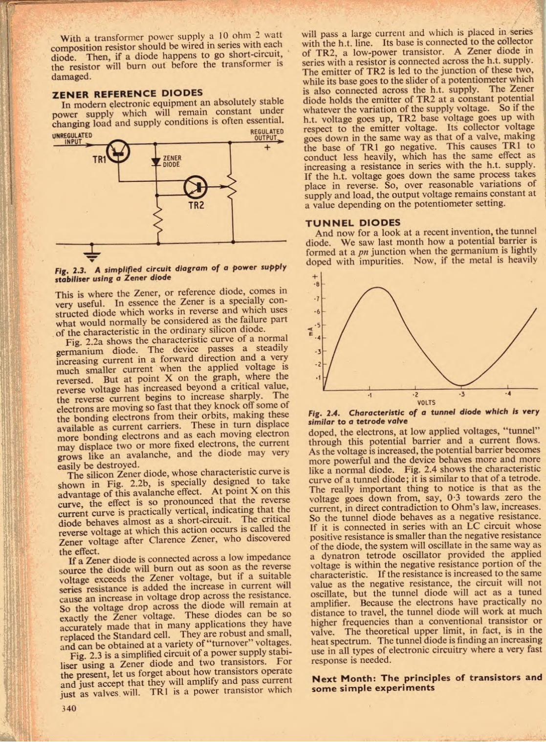
TUNNEL DIODES
And now for a look at a recent invention, the tunnel
diode. We saw last month how a potential barrier is
formed at a pn junction when the germanium is lightly
doped with impurities. Now, if the metal is heavily
VOLTS
Fig. 2.4. Characteristic of a tunnel diode which Is very similar to a tetrode valve
doped, the electrons, at low applied voltages, "tunnel"
through this potential barrier and a current flows.
As the voltage is increased, the potential barrier becomes
more powerful and the device behaves more and more
like a normal diode. Fig. 2.4 shows the characteristic
curve of a tunnel diode; it is similar to that of a tetrode.
The really important thing to notice is that as the
voltage goes down from, say, 0-3 towards zero the
current, in direct contradiction to Ohm's law, increases.
So the tunnel diode behaves as a negative resistance.
If it is connected in series with an LC circuit whose
positive resistance is smaller than the negative resistance
of the diode, the system will oscillate in the same way as
a dynatron tetrode oscillator provided the applied voltage is within the negative resistance portion of the
characteristic. If the resistance is increased to the same
value as the negative resistance, the circuit will not
oscillate, but the tunnel diode will act as a tuned
amplifier. Because the electrons have practically no
distance to travel, the tunnel diode will work at much
higher frequencies than a conventional transistor or
valve. The theoretical upper limit, in fact, is in the
heat spectrum. The tunnel diode is finding an increasing
use in all types of electronic circuitry where a very fast response is needed.
Next Month: The principles of transistors and
some simple experiments

By S. Chisholm
The information which follows describes the proto-
type, which employed complex tone control. As the
equipment is not frequency-conscious, rigid adherence
to component values and dimensions is not essential and
the prospective constructor will probably find some of
the material on his spares shelf already.
It must be realised, however, that there is a very high
gain between input and output; when designing layout,
cross-coupling between grid and anode circuits due to
close proximity of wiring will cause instability. Also,
because of the high gain, the main amplifier must be
effectively earthed if hum is to be reduced to a minimum.
The earthing arrangements must be adhered to in the
sub-units and input circuit screening.
MAIN AMPLIFIER
Fig. 5 shows the drilling details of the main amplifier
using international octal valve bases. It does not show
drilling details for component assembly strips, T3, L3
and L4 as these will depend on what is available.
Fig. 6 shows a representative component layout when a
smoothing choke is to be used instead of an energised
loudspeaker. The location of the transformer (T3) is
shown doited, also the position of L4. Approximate
cable entry positions are given.
As much as possible of the wiring to the grid circuit of
V3 and to the compensating volume controls mounted
on the relay sub-assembly should be in screened cable.
The screens are earthed.
A word of caution here: in some screened cable
(particularly coaxial cable) with p.v.c. or polythene
insulation, the insulation will melt at fairly low tem-
peratures. It is best to tin the screen and centre
conductor with solder before final connection. In all
cases, check the insulation between the internal lead and
its screen after completing the joint, making sure that
no resistors are in circuit.
When wiring, do not forget the h.t. and l.t. con-
nections for the sub-units. These can be formed into a
cable, in which the heater leads should be a twisted pair.
Finally, ensure all joints are sound. One poor con-
nection can cause a great deal of annoyance and partial
dismantling of the assembly. A good test for "dry"
joints is to give the soldered wire a gentle tug with a pair
of pliers.
COMPONENTS
Details of components were given last month but it
may be worth mentioning here that if R28 is too low in
value the vibrato speed may be affected.
Relays RLA, RLB are mounted on a sub-panel which
also carries the compensating volume controls. The
flexible wiring from the relay contacts to the amplifier
must be low loss screened cable in anode and grid
circuits and may be laced into a cable form which
enters the amplifier through a suitable grommct.
Wiring between the relays can be single strand p.v.c.
covered wire.
PRE-AMPLIFIER
A typical layout for this sub-unit is shown in Fig. 7
and needs little explanation. Healer wiring should
again be in twisted pair. Grid inputs, and anode output
leads to the main amplifier, should be in screened
343

wiring, the screen being well earthed. Remember to
leave sufficiently lengthy leads for inter-wiring between
the pre-amplifier, the vibrato panel, and to the input
control panel. These can be laced after the units
have been fitted into the cabinet and the connections
soldered. • a
A word of caution regarding valves. It is advisable
to use new valves if possible. The reason is that some
"used" but "good" valves are too noisy for those stages
where high gain is required. A cathode to healer leak
is one source of noise here, whereas it may not matter so much in later stages of the amplifier. The valveholders
should be skirted, and have clip-on screening cans both
to prevent hum pick-up and to prevent the va ves becoming dislodged during transit. A small bracket,
boiled to the skirt, provides a simple means ot attaching
the holder to the sub-unit panel.
VIBRATO UNIT
This unit is shown in Fig. 8. The capacitors in the
prototype were physically rather large and a suggested
alternative layout is shown in view of this. Construc-
tion is on similar lines to the method described for the pre-amplifier. _ .
Transformer T1 is an inlervalve transformer whose
secondary d.c. resistance is approximately 2,(XX) ohms,
and primary resistance about 500 ohms. Other steP"yP transformers have been tried and worked quite well, but
the one specified above proved most effective. Its
function is to control the vibrato "slow" frequency,
thus a small amount of experimenting with readily
available transformers and capacitors may be necessary.
If a selection of transformers is not available, a 4:1
step-up inlervalve transformer should be obtained.
The resistor R15 will determine the amplitude (depth)
of vibrato; try 20 kilohms for a starting point. If "puffing" (over-modulation) of the vibrato occurs,
raise the value in 5 kilohm steps until the puffing clears.
INPUT CONTROL PANEL
The component layout of the input control panel is
shown in Fig. 9. Physically small potentiometers are
required in order to clear the sockets SKI, SK2 and
the control socket SK3. Wiring between the panel
and the sub-units is made up into a cable form, which
includes screened leads from VR1 and VR2, and is
secured against vibration by the insulated cleat; other
leads are clamped to the interior of the cabinet.
The h.t. and l.t. supply leads coming from the main
amplifier are also assembled into the cable form, but
remember to twist the l.t. leads. Lamp LP1 is a 6-3V
0-05A, or 0-3A if the transformer can handle the total
load quite safely, and indicates when vibrato is in use.
GENERAL ASSEMBLY
The overall assembly of the complete amplifier was
shown in Fig. 2 (last month). Note the positions of
the vibrato speed control VR3, the smoothing choke
Fig. 5. Main amplifier chassis. Power supply components are not shown since their position and drilling details depend on the sizes of the Items used. CABLEFORM L3 is not shown for the same reason, EMTW A guide to the approximate posi- tlons Is given In Fig. 2 ^ ^
ON/OFF VOL.)
TONE SWITCH SZ If mounted on chassis
k V \
N
N MAINS CABLE ENTRYv 2*
OUTLET' V CabktopaneU^
control i
•N
3! POWER SUPPIY TO SmHJHfTS
5/7
TO OUTPUT TRANSFORMER M
DIA.0N * HOLES 5/x0 <VCENTR&
HOLES ABA CLEAR. ft'C'HOLES^OU. i%tf HOLE 'JA OU. S'E*HOLES iVsOIA.
ZVnOLES TO SWT 2 F SOCKET
344

V4 vs V6 FtfO
-\R? N _ — t — V N
' I / T3 m R^
\^Cl8l^
CZIx
. CM R?l
r' JRzsci:
R24 ^ U* I
CI9 CI60 k C20 lU m
Fig. 6. Approximate layout guide to components on the underside of the main amplifier chassis. L4 and C2I are fitted only if the complex tone control circuit (described last month) Is used. The approximate positions of T3 and L3 are shown; they are mounted on the top of the chassis. The cores should be arranged at right angles to each other to reduce hum
L2 and associated capacitors C8 and CI1. These
items (including R19) cannot be fitted into the
sub-units or main amplifier without overcrowding or
risk of hum due to coupling. The terminal strip
secured to the loudspeaker carries the wiring to the h.t.
fuse mounted on the main amplifier control panel.
The relay sub-assembly can be conveniently fitted
above the top edge of the amplifier control panel.
From this point, the wiring (in the cable form) to the
main amplifier is quite short and, if handled carefully,
the relay sub-assembly and main amplifier can be
withdrawn for inspection without unsoldering.
Security of the sub-assemblies can be obtained by
fitting a wood or metal pillar to the cabinet adjacent to
the side of the sub-assembly concerned, and then
securing the sub-assembly panel to the pillar by a screw
passed through the panel. This precaution is worth
taking if the amplifier is to be transported frequently.
The vibrato and tone controls shown on the guitar
(January issue) are SI and S2 respectively (see the
components list last month). If desired SI can be
mounted on the control panel of the amplifier as shown
in Fig. 9. S2 can be mounted on the main amplifier
chassis as indicated in Fig. 5. In this case the inter-
national octal control sockets can be eliminated so that
only one screened cable is left to link the guitar volume
control with the amplifier.
EXTENSION LOUDSPEAKER
If the lid of the cabinet is used to house an extension
loudspeaker, it will be necessary to fit a hardboard
panel over the interior of the amplifier to guard against
damage when the extension speaker is in use.
TRYING OUT THE GUITAR
Fit the guitar plug into the guitar socket, and the
control plug and input plug into the amplifier sockets.
Switch the amplifier on and allow time to warm up.
Set the amplifier volume control to about mid-travel.
Set the tone switch to normal, and the gain controls to
two-thirds of full travel. Set the vibrato switch to off.
Set the guitar volume control about mid-way and the
tone switch to the central position (normal tone). Set
the vibrato switch (SI) to "off". The central position
gives slow speed; downward gives fast speed.
Now pluck the strings and adjust the volume control
to the required level. If insufficiently loud, increase the
input gain control (VR1) on the amplifier or, if this is
already at maximum, set the main amplifier volume
control to a higher level. Check the effect of the tone
control and note the switch positions. Check the
vibrato circuit at low speed and high speed and note the
switch positions. Adjust the bass and treble gain to
balance volume when using normal tone.
USING THE AMPLIFIER
(1) Ensure the amplifier is efficiently earthed by as
short a lead as is practicable.
(2) Switch on 10 minutes before requiring to use the
amplifier to allow it to settle down.
(3) If using only one input, turn the unused input
volume control to minimum otherwise hum may
be picked up. This effectively shorts the grid of
the other half of VI to earth.
(4) Vibrato is most effective on sustained notes.
Do not try to use it on fast moving music.
(5) To prevent excessively noisy operation, use no
more input gain than is necessary.
(6) When using a microphone, which must be a high
impedance type, or a low impedance type coupled
through a transformer, guard against acoustic
feedback, especially if two speakers are in use,
v« V5
ffl m aa R1 ^ R8 R7 R<0 R<Z R9 RIT
^ 1
A© B© C0 D0 E0 F0 G0
Fig. 7. Pre-amplifier unit built on Veroboard. Terminal connections are as follows (see also Figs. 6, 8, and 9): A to LI, Cl; B to RI5 (and L2 see text); C—coaxial to RI7; D and E to heater supply; F—coaxial to VRI; G—-coaxial to VR2
345

otherwise the loudspeaker may be damaged.
For high quality, a crystal microphone should be connected through a matching circuit to suit a
50 kilohm input impedance.
ADDITIONAL GUITAR DETAILS
The following notes may help readers who are
constructing the guitar described in the January issue.
Head Matching Transformer
This component is mounted in the body of the guitar,
so the most critical feature is its physical size determined
by the space available. It should preferably have a
voltage ratio 30 : 1; a microphone transformer
should serve the purpose. Alternatively, a loudspeaker
output transformer with a 3 ohm low impedance
winding can be used provided the impedance of the
other winding is at least 2,700 ohms.
It may be worthwhile providing one channel of the amplifier to take a high impedance input while the
other channel can be low impedance. This trans-
former can then be mounted on the amplifier chassis
and wired to one channel only, keeping the same
physical connections as described earlier. This means
that the "sound" lead from the guitar will be low
impedance and reduce the likelihood of hum being
picked up. The restriction of physical size is also
overcome.
Guitar Volume Control
This is a miniature carbon potentiometer cither
25 kilohms or 50 kilohms. Here again the physical
size is important. The higher resistive value will give
a coarse cpntrol, i.e. a faster reduction of volume.
Strings and Winders
The strings used arc standard taped strings specially
made for electronic guitars (they must be steel) and are
readily obtainable in sets of six from music shops
dealing in guitars. The winders or "machine heads"
arc single units secured to the instrument as described
in the article. The string is passed through the hole
in the winder pin which is attached to the spur wheel.
There should be sufficient slack in the string to give at
least two turns around the pin before the strings become
taut. The turns should be low down on the pin.
O SM LPI
SK5
& (D
CABLE FORM
B © |SK2 VR? Si
CI&C?
/ m
u % n
w. Q
cv K'- i RJ fni
V2 M - *
RI5
© 0 0 *0) 9
Pig. 8. Vibrato unit built on Veroboard. Terminal con- nections are as follows (see also Figs. 6, 7 and 9): A to R2; B to R4, RIO, RI2; C—coaxial to Sib (I); D and E to heater supply; F to VR3 (mounted on cabinet). Screen
of coaxial cable to chassis
Fig. 9. Control panel layout. Socket SK3 links with the remote controls on the guitar. Sockets SKI and SK2 ore the signal input jacks
GUITAR FAULT ANALYSIS
One or two points may be mentioned in conclusion,
and may help a constructor to overcome difficulties or
avoid pitfalls when using the guitar.
Falling Out of Tune. Check the condition of
storage; a damp room will cause this. Check for
curvature of stem due to soft wood; check the move-
ment of the stem due to insecure fixing screws or to
very soft shim m'aterial. Check for movement of lail-
plalc; the body must be very sound hardwood other-
wise it will allow the tailpiece to drag its screws.
Inaccurate Tuning Over the Range o) Frets. This is
due to (a) use of incorrect string for the position, or
(b) inaccurate measurement and placing of frets. Try
moving the bridge block to correct mistuning.
Low Sensitivity Over-all. Check that the strings are
steel strings (internally, if wrapped) as used in electronic
guitars. Nylon strings are useless with a pick-up.
Low Sensitivity at One String. This is likely to be
due to a short circuit when winding the pick-up limb
concerned. It will require rewinding.
No Output. Pick-up winding broken, or circuit to
transformer broken or short-circuited. Check from
transformer by removing fingerboard, connecting up
the amplifier in the usual way, and with the volume
control set high, touch the transformer terminals.
Touching one terminal should produce a loud hum.
If this is not so, check the wiring to the volume control,
the connector cable and the input plug.
Greater Sensitivity at Low Notes. This is probably
due to the string material, but may be partly or wholly overcome by increasing the height of the affected
string above the pick-up. The height may be increased
by alteration to the bridge slot. Feedback. A sensitive guitar, played very near to
its loudspeaker, will pick up notes to which the *'open"
strings will respond. This causes the strings to vibrate
and produce a continuous, often unpleasant, note.
The volume control should be decreased or the loud-
speaker may be placed further away from the guitar
and facing away from it. ★
346

The unit to be described is basically very simple, and
yet extremely useful for the motorist without a
^If*a car fitted with this device is parked in a street,
the parking light will go on automatically when it
begins to get dark. This saves the owner the task ol
having to come out and switch them on at lighting-up
lime to avoid a "ticket" for parking without lights.
Not only does this unit switch the lights on in the
evening, but it also switches the lights off in the morning
when it is light.
CIRCUIT v . t
The heart of the circuit (see Fig. 1) is the very sensi-
tive OCP71 pholotransistor, which combines the
advantages of a low voltage photocell and a built-in
transistor amplifier all in a single envelope.
The signal from the pholotransistor TRl is passed
to a multistage, directly coupled transistor amplifier,
in emitter follower configuration. The number o!
stages employed in the amplifier depends on the
characteristics of the relay used, which will be dis-
cussed later. Bias is supplied to the pholotransistor
via VRI, which controls the operating point of the
whole circuit. Note that R2 has a negative temperature
coefficient, to compensate for changes in temperature,
and is, in fact, a thermistor.
RELAY • r J .u I The output from the amplifier is led to the relay
RLA which must be as sensitive as possible, with the
energising coil rated at 12 volts. The contacts need
not have a high current rating; a single-pole changeover
type rated at 12V 1A being suitable. . . r
Before building the amplifier, the vital statistics of
the relay must be assessed, as these govern the number
of stages used in the amplifier.
Find the current needed to energise the relay, and
also the current at which it "drops out", i.e. becomes
de-energised. The smaller the difference between these
two current values, the more suitable is the relay.
This is because the changes in light intensity produce
changes in current in the pholotransistor which are in
turn amplified by TRl and TR2. It this change in
output current is not enough to take the relay from the
"on" position to the "off" position (or vice versa) the
unit will not function correctly.
The relay used (type MH2, 700 ohms) was found to
operate at about 12mA and drop out at about 4mA.
CONSTRUCTION
The construction of the unit is not critical, and with
small components can be built in a surprisingly small
space.
The whole unit can be built up on a 15-way miniature
component lag strip with the switch and potentiometer
mounted on the side of a plastics box 2jin x 4iin
(see Fig. 2). . . .
The pholotransistor TRl can be mounted through
a hole in the stem of a rubber suction pad and soldered
to a length of twin-cored screened flex, as used
in record players, etc. This enables the pholotran-
sistor to be mounted in a suitable position on the car,
while the amplifier and relay unit is hidden away out
of sight The most light-sensitive side of the OCP7I is the
base-emitter junction (recognised as the side of the
base with the smallest "blob" on it). The collector
wire is the one nearest the white line at the side of the
plastics envelope.
et so m in Nl time ar
itsel light switch parkin et your
^yr^rrnyF1 ^ 1'1 l,fi 1 ^
CfaOESKEOJI
* L
♦
[BSIHffX]
LIGHT
347

I
R! RJ ikSi 0\W P1 A 17
Rl At
TR2
Parking lamp 0C8ID 0CP7i
VRt
250 kfi
¥
R2
.7 k A
Th«ri«Dtof
Fig. I. Complete circuit diagram of the amplifier and relay unit. Note that R2 Is a thermistor which compensates for any changes In temperature
a
Fig. 2. This version has three leads coming from the platlcs box enabling the unit to be hidden away. The three leads are: one from the relay to the parking light, one from the unit to the car battery, and finally a lead from the unit with the photocell soldered to the end and In- serted through the end stub of a rubber suction pad for mounting In the car
Fig. 3. In this version one lead from the car battery to the unit Is the only exter- nal connection. The photocell and parking light are mounted in or on the transparent plastics box. Although the mounting is much simpler there is the added risk of theft since the complete unit is mounted on the window
348
*
T B

PorkinqU^t
H2 TR3
-fKV O a o o ■
m* t -t?v
RL A ; ■■.' -
51
^4 to
H(
Fig. 4. Component wiring lay- out. Note that ten tags are removed from one end of the panel to accommodate the relay
COMPONENTS...
Resistors Rl 4-7kn iW 10% R2 4-7kn thermistor R3 IkQ iW 10% VRI 250kU miniature pre-set potentiometer
Transistors TRI OCP7I phototransistor
TR3 OCs! ^j0r s,m''ar a^* transistors
Relay RLA Sensitive energising coil, 12V, 700ii (Type
MH2, Keyswitch Relays Ltd.) Single-pole changeover contacts rated at 12V I A.
Lamp LP Parking lamp 12 volts 0-5A amp
Miscellaneous 15-way component tag strip, on-off toggle switch, wire, plastics case
Readers may have their own ideas about housing
the unit, but to keep the wiring to the battery and lamp
to a minimum the box should be close to them.
SETTING-UP
Set VRI anticlockwise (lowest resistance) and connect
the relay coil in series with a 0-25mA meter. The meter is
used merely to check that excess current is not being
drawn.
Place the phototransistor, on the end of its lead, in
normal daylight (not direct sunlight). Advance VRI
slowly until the relay is just heard (or seen) to click in.
This should be the correct setting for VR1.
Any decrease in the light intensity will cause the relay
to drop out, and thus switch on the parking light via
the relay contacts. Check that the current taken by the
relay is within the range previously mentioned. The
amplifier should take only a few milliamps more.
The current taken when the phototransistor is in the
dark should be quite low, only a few milliamps.
If the phototransistor needs almost complete dark-
ness to switch off the relay, either VRI is set too high
or the amplifier or relay is not sensitive enough.
One word of warning: it is possible that the street
lighting, if powerful enough, may interfere with the
correct function of the unit, so the transistor should
be shielded from it. ^
PRACTICAL WIRELESS PRACTICAL TELEVISION
THIS MONTH
THE "CADET"
A 7VV hydrid amplifier, using transistors for low
signal amplification and a valve output stage.
KEYED AUDIO OSCILLATOR
A versatile unit for the experimenter.
VOLTAGE STABILISED V.F.O.
Special feature for "hams".
March issue on sale NOW. Price 2s.
THIS MONTH
DO-IT-YOURSELF GUIDE TO TV SERVICING
Instructional article for the newcomer.
GSNOX/T
The well known amateur television transmitting
station.
IMPROVING THE P.T. C.C.T.V. CAMERA
Further notes on this popular feature.
March issue on sale 18 February. Price 2s.
349

\*zr
□
D
I I
ENE * i
What A Dish!
, >
The 2IOfl radio telescope at Parkes, New South Wales,
has acquired a new friend
recently in the form of a 60ft
diameter infcromelcr (seen on
the left of the picture). This inferometer is, to a cer-
tain extent, mobile since it runs
on a system of circular and
straight quadrant tracks. It is
capable of providing an addi-
tional degree of accuracy in
finding the position of radio
sources in the universe, including
artificial satellites.
This inferometer has been
financed by the Commonwealth
Scientific and Industrial Re-
search Organisation, which also
designed it.
500 MHO f
c »
- * *
o o
OdO
<?
o
»r * 'I i . >»'!
Precision Communications Receiver
rouR YEARS of research and development by the National Radio Company r in America has culminated in this HRO-500 commun.calions receiver.
No less than 57 semiconductors arc employed in solid stale plug-in circuits
to cover 5kc/s to 30Mc/s. Frequency stability is maintained to a high order
bv a phase locked synthesiser with a crystal controlled oscillator. The receiver can be operated on s.s.b., c.w., or a.m. Provision is made for
remote control use and it can be powered by 115-230 volts a.c. or 12 volts
d.c. It is said that the performance is commensurate with the price for such
an advanced piece of equipment. A . A _ . . . Distribution in the U.K. is being handled by Ad. Aunema Limited. The
price—£606 2s. 9d. retail. Strictly for affluent hams!
4
« i i
• . ■ / ' -
\\y a i / i.
If- A i < i I..,
wmk

...
, | wmmt
-
I'
V
/
■>
/■
Look After the Pennies... ^
Five computers, designed and built
by English Electric Leo, and worth
£2i million, will help the Post OITicc
look after its accounts, including the
savings bank and premium bonds.
From 1 January next year the charac-
ters on postal orders will carry a
magnetic ink so that coded details can
be t'filcd,, on magnetic tape.
Don't Dig That Road!
Anew way of increasing the
number of speech channels be-
tween telephone exchanges without
digging up the road has been under
investigation for a number of years by
the Post Office. The outcome is a
system of transmission by pulse code
modulation which was first invented
in 1937.
Now Standard Telephones and
Cables have built equipment for trials
over the cable route between Guildford
and Haslemerc in Surrey. Up to
twenty-three speech channels can be
accommodated on a four wire circuit
with one pair carrying the "go"
channels and the other the "return"
channels.
Speech from each of twenty-three
subscribers is sampled sequentially
8,000 times per second. Each sample
is measured against a 125-Icvel scale
and a coded pulse train is produced
corresponding to the level of each
sample. Pulses are transmitted at
1,750,000 per second along the line.
A 24lh channel is used for syn-
chronisation. Repealers can be
installed in existing manholes to boost
the signals. The pulses received at the
other end are decoded and transmitted
as "real" speech on twenty-three
lines.
And they don't get mixed up!
Ghost Train! The modern idea of a driverless train is by no means
confined to the London Underground Railway. This
particular model, designed by E.M.I. Electronics and in use
here at their record factory, runs on any kind of road
surface which has been fitted with a special "live" wire.
The Robotug, as it is called, detects the current flowing
through the wire, which is buried half an inch below the
surface, and steers itself according to the signal received
from it. As it reaches a point where it needs to cross the
road a traflic signal is automatically switched to red to
hall ordinary vehicular traffic.
After crossing the road the signal reverts to green.
The factory doors are opened automatically when the
Robotug approaches. If the train is delayed en route
for more than 10 seconds an alarm signal is set off.
*
n
ff * 4
'■
•» r
r
S
m H
P¥1
■>
A
%
V % IN * * ■s
v V
-v
%
* * %
i'»> • i
H

BEGINNERS start here... 5
An Instructional Series for the Newcomer to Electronics
Resuming our discussion on the capacitor, we first
note two basic but vital formulae which enable the
total value of capacitance to be calculated when two
or more capacitors are connected in series or in
parallel.
CAPACITORS IN PARALLEL
Last month we saw that one of the factors which
determine the amount of charge stored in a capacitor
is the area of the plates. Increase the dimensions of
the plates and the charge stored increases—or in other
words the capacitance of the component increases.
From this it will not be difficult to see that when
two or more capacitors are connected in parallel, as
shown in Fig. 5.1, the total capacitance is then the sum
of the individual capacitances. The formula is given
below.
i
ci :n
XJ"
C total — Q + C, + C3 etc.
Fig. 5.1.
CAPACITORS IN SERIES
If a number of capacitors are connected in series, as
in Fig. 5.2, the resultant value of capacitance is
calculated using the formula:
C total = 1 \ 3—t etc. C4
C2
C3
1 +JL+ J Ci c, ca
It will be noted that the formula
for capacitors in parallel is similar to
that for resistors in series, while the
formula for capacitors in series is
similar to that for resistors in
parallel.
Fig. 5.2.
PAPER AND FOIL
These capacitors, commonly referred to as "paper
type, are inexpensive and are widely used in medium
capacity values of from about 0-0001-1/^F, although
higher values are obtainable. Capacity value tolerances
are 10 per cent and 25 per cent. They are made in
various d.c. ratings from 150V to 1,000V and even
higher.
Paper capacitors are ideal for audio frequency (a.f.)
purposes but have a fairly poor power factor (0-25 per
cent) which makes them rather unsuitable for the higher
frequencies. A certain amount of inductance is often
present and this is a further limiting factor as far as
the higher frequencies are concerned.
Paper and foil capacitors are made by winding strips
of aluminium or tin foil with interleaving strips of
specially treated paper. The strips of metallic foil
form the two electrodes or plates of the capacitor and
they are insulated throughout by the paper dielectric
which is impregnated with paraffin wax or other
material to prevent the absorption of moisture. The
completed toll is hermetically sealed in a tubular case
of cardboard or metal. The cardboard cases are
usually coated with wax. Metal cased types are often
covered with a plastic sleeve.
METAL FOIL
TERMINAL STRIP
TERMINAL STRIP
'PAPER
Fig. 5.3. The general form of construction of a paper and foil type capacitor
PRACTICAL CAPACITORS
We will now proceed to look at practical capacitors
—the actual components one meets in everyday work
on electronics. One expression that crops up several
times in the following brief descriptions is "Power
Factor". Do not worry about this term at present;
we will explain the meaning of power factor later. As
you will soon discover, there is a large variety of types.
Each type has its own particular advantages and
disadvantages. We must learn about their character-
istics in order to be able to choose the most suitable
capacitor for a particular purpose.
352
It is becoming more the practice now for these
capacitors to be encapsulated in a plastic tube. This
kind of housing is generally more effective, particularly
at high temperatures, where there is always the possi-
bility of wax melting. The moulded plastic container
also permits a reduced overall size as compared with
the conventional tubular capacitor.
With the larger values, from about 0 01 to 10/aF,
the roll is pressed flat and then fitted into a rectangular
metal case.

metallised paper This is a development from the paper and foil tvne
formsW,]erC 3 ,hin deposit of on the paper
Due L this £heS? ,nStead 0f seP;ira,e metallic foils.
S made fnf n a ""T® C0lI,Pact component can oe made for a given value of capacity. Another
aluable feature of the metallised paper capacitor is
volta«f4L0onrlhSla^d the app,icali'n of excessive vonage without sustaining permanent damage.
r.SKh^?50W3SSS m0m™n' Wi,h V;,l,a8e
PLASTIC AND FOIL
SUbsti^pn,fnrVeIOPmentJS 0f PlaStiC filmS aS a substitute for paper. Plastics such as p.t.f.e. nolv-
ihpm"6 a." i,0,,yCSter have characteristics which make
&H^rtr,ar,y sultabIe as a dielectric material. The sid
8erdufjC^c st.ren8th of these plastics permits a con-
=b,fv^10n.- Ph>:sical size compared with a
ta^ tyTm^'T 0 equivalcnt va'ue- Good anH c- 18 maintained over a wide temperature range
^naS arP^T'r'8 imPervious 'o moisture thefe
SmS humidhy! ^ 0Perat,0n Under COndi,ions
annmx'imMiHv th' CaPacitors are manufactured in
paperType. Same ran8e 0f values as the
An interesting range of low voltage workinc
capacitors specially designed for close packing on
years In^their r haS beCume P0Pular in recent ^i . • n
fi,thei.r components, the winding of foil and
shaS nf IS uaUCuIled 80 ,he component takes the shape of a small tablet. Insulation and protection
IS provided by a hard lacquer coaling.
METALLISED PLASTIC FILM
thc^ameSmlaftic f0.il (polycstcr> capacitors follow IvL! k construction as the metallised paper
and from ^mre 'h US- COmpleItcly insulatcd electrically
m..h h at.mosphcr|c conditions. This moulding
mmnnn.mc 8 3 Var,ety of shapcs' and rectangular components are common; these are of course very
Twif11 C Se packing of components is necessary. n m f ^ -/^ngCS 0 mcta',ised plastic capacitors are 0 01 to 2-2//F 160V; 0 01 to 0-47//.F 400V
In this particular range one connecting lead is con-
mounting. 8er thC 0ther and facilitatcs vertical
IVM-'Thaw Th,alfiSMd p(,lyesI<ir caPacitors ("flattened n i^p Tk i. following values; 0-01, 0 047 and 0 l/^r. The voltage rating is 200V.
MICA STACKED FOIL
foi1|natreiSclt™HftCaP^it0r ^ of mica and metal toil are clamped together to make a compact stack
Alternative layers of foil arc connected together thus
forming the two electrodes. The stack is enclosed in
a moulding through which are brought out two con- necting wires or terminal lugs.
METAL FOIL
■ 'e;.5:4- Alternate layert of mica and metal foil are stacked in this manner to form a capacitor "oc*e<»
Mica is the best of all the solid dielectrics, but it is
at *P!:|lSIVe a," bu'ky. and so its use is conlincd
to 5 OOOnF rn 0 Capaci'y' ran8ing from 5pF ^rc . P '0 ()05/'F) approximately. These capaci-
m 07 ^ very stable and have a very low power factor
Th^ y or lower) and arc ideal for r.f. purposes
abounSO.'"8 VO 380 0f ,hCSe capacitors 'S normally
SILVERED MICA
f ™LSilrVCrCd mica or metallised mica capacitor is
kl^T .u onc or more pieces of mica coated on both sides with a thin film of silver. In the case of multiple
plates these arc stacked and all the upper coalings are
connected to one lead-out metal stripedTower^ott,-
^ ■ -lse to another wire. The assembled capacitor is either encased in a moulding or is given a protective
coating of wax. Miniature types can be obtained with
the conventional axial connecting strips or with side
Sg^ands Particularly suitable for printed
SILVER DEPOSITED EITHER SIDE OF MICA PLATE
in ^r?d mica .^Pacdors have marked advantages m that they arc little affected by time or temoeramm
and they should be used whenever a precise value
of capacity and a higher order of stability arc essential
mqnU|l7ec?n,S J VallJCS range from l -5pF to I2 000dF (0 012//F), and tolerances of 1 per cent, 2 per cent or
10 per cent can be obtained. Voltage rating 350 500
Power factor less than 20 x 10 ' per cent '
CERAMIC
Ceramic has a high dielectric constant and the use of
o Th enables a range of lowcr valuecapadtore having very small dimensions. A variety of
St ,«HUSed " al1 ,he basic method of construc- on is to deposit a thin metallic coating on two surfaces
of a ceramic plate, tube, disc or cup. Two someS
^"'tLSeTrovidc |lhad',hr0U8h ,ype- and a stand-off type, tnese provide the answer to many constructional
requScna|t.ar,Se ^ dCSi8nin8 the layou, of a pi**
METALLIC COATING CONTINUOUS WITH INNER COATING
METALLIC COATING
INSULATING MARGIN
Fig. 5.6. A tubular ceramic type capacitor
There remains yet one more important tvoe of fixpH
N"f -.on". ™ S
353

•. •
o oom/r
f A rA
m
m
By A. SYDENHAM
In (he electronics sphere transistors arc considered to
be one of the most important advancements since
the war. Miniaturisation of hitherto cumbersome
apparatus is made possible and efficiency is improved.
In domestic entertainment they provide an excellent
means for building small inexpensive units for adding
to existing equipment. The aim of this article is to
present a reliable device, in simple form, that can be
used to detect broadcast signals and feed radio pro-
grammes into a tape recorder. The unit can also be
employed in other ways as will be explained later.
Considerable attention has been given to design and
presentation and the outcome is a unique unit, fully
portable, and weighing only 12 ounces. It is com-
pletely self-contained and is powered by a small
battery which will last a very long time due to a low
current drain of only 2mA. Programme material over two wave bands is available
and switching is so arranged that the chances of
accidentally leaving the unit switched on arc minimised.
From the constructional angle care has also been taken
to utilise only those items easily obtainable.
The minimum number of small tools needed to
complete the project are required and a "kitchen table"
construction is feasible if needs so dictate.
RECORDING FROM THE RADIO
First attempts at making recordings frequently
consist of little more than placing a microphone in
front of an operating radio receiver. Fig. 1 depicts
various ways in which recordings can be made, the
simple scene just mentioned being shown in Fig. la.
Provided room noises arc kept low very good results
arc possible when the programme material is not
musical in content. Microphone recording is without
doubt a convenient method but it is best left on one
side if music is to be recorded with any degree of
fidelity. Quality can be impaired if the loudspeaker in
the radio set, the microphone, and the room acoustics
are not perfectly loss free over the audio frequency rangC<
A slightly better method is shown in Fig. lb but this
too has its drawbacks for it is soon realised that any imperfections present in the sounds issued by the
loudspeaker arc truly copied on to the tape.
354
To obtain distortion free signals from a radio
receiver it is necessary to extract them from the part of
the circuit where they are comparatively pure—for
example, at "w" in Fig. Ic. Sometimes an existing
receiver can be "adapted" to provide the take-olT points
but in many instances it is wiser to build a separate
unit.
Main requirements of a unit such as the one des-
cribed later are:
1. The device should be tuneable over both medium
and long wavebands.
2. It should be small physically.
3. It should be self-contained.
4. It should be versatile so that it can be used with
other reproducing equipment.
All the above requirements are fulfilled in this
article. For even better quality reproduction a v.h.f.
f.m. tuner is recommended.
A B
0 o Tone Voi Tone
(o)
I
V G r* — Extraneous V* P " — no«s«s
Microphone
N \ \ (Low quality si9nob)
To Recorder \l/
c
N
\1/
To Recorder (Medium quality signals)
A
' B A
\ O 0 •
c)
\
To Recorder
Fig. f. Methods of recording from a domestic receiver

CIRCUIT THEORY
The theoretical circuit is given in Fig. 2 and shows a
3-transistor grounded emitter configuration in which
TR1 accepts signals selected from the aerial trans- formers LI and L2. The mixer stage introduces a
frequency changing action to produce a lower frequency of 470kc/s by combining the r.f. signal with a local
oscillator signal. TR2 and TR3 amplify the resulting
signal with the aid of tuned intermediate frequency
(i.f.) transformers.
Diode D1 rectifies this signal and makes it audible. The diode also causes a voltage to be developed across
resistor R7 during the rectification process and this
varies in proportion with signal strength. By feeding
back this voltage to the transistor TR2 an automatic
gain control circuit is set up increasing the effective
output of weak signals; strong signals are auto-
matically reduced.
The board must be drilled to accommodate the four
canned transformers (as shown in Fig. 3); the strips
and holes have been given reference numeral and letter
designations. If a ^in diameter hole is cut out for each
transformer exactly as shown it will be found that the metal cans will stand comfortably on the plain side of
the board, allowing the pins to project below; the dust
cores will also be available from either end. The
transformer mounting lugs may then be passed through
existing holes, for instance, the lugs of T4 will engage holes 3d and 6d and so on. These lugs are then bent
over to lie along strips 3, 6, 9. and 12, but note the
orientation, especially with regard to Tl, before
soldering.
A hole must also be cut out for the shaft of VCI as
shown and the conductor strip must be severed as
indicated at points w, x, y and z. The shaded portions
at the opposing corners must also be removed. The
TR2.5 TR1 T? • r T5 14
0 r
0 Ri i i
b c * b v Spot 47 22 kCI Tl 3- T2.3(4 KQ
SI
U LONG WAVE_ L2 MfOIUM^VME
::+ Red White
IO.OOOPL £•
Gretir How Blue 0A7C
TR1 TR2. TR3
Rll ISOpF — AAA/,
1.2 kn
Ju 220 AF«7 AFH7 PF e i a:
T 0044 /■
R2 8-2 kfl :ic 3
JVS SIA SIC n ICO C0 PF
.aoooTR3
pF 3-9 P "TwuF '176 R9 8uF R6 04 R1C .04 04 pF pF uF IWl •s ' uF yt
A kd kD
I -J RS Battery 9V
-w OUTLET
175?F (see text) SIA.B.C ganged
1-Medium wave 2-Off 3-Long wave
NOTE a2ka Trirrmer capacitors not shown are inbuilt with VCIA/B.
Fig. 2. Circuit diagram-of the tuner. Undesignated capacitors onJT2. T3. and T4 are supplied inside transformer cans
We could take the audio signals for our recorder via
€6, where little signal distortion will have been intro-
duced. If on the other hand, we connect a pair of
high impedance headphones (say 4,000 ohms) to the
output socket, signals may be plainly heard. Or. we
could connect a suitable audio amplifier to the socket.
CONSTRUCTION
The unit can be easily built by using a piece of
Veroboard (approximately 2$ x 3iin) with holes
spaced 0-2in apart, it is thus very easy to link
small low voltage components together to form a
pseudo "printed wiring" assembly. The particular
piece of board required should carry 14 conductor
strips each having 19 holes; this is easily cut
from a larger sheet by using a hacksaw, or a piece
ready cut to size can be purchased.
various connections shown in Fig. 3 arc then made
exactly as shown.
Most of the components occupy the plain side of the
board; their locations arc shown in Fig. 5, which also
shows the board correctly positioned for mounting on
the inside of the front panel.
P.V.C. sleeving is fitted to each transistor wire, which is then held firmly with strong tweezers during the
actual soldering process so that heat is shunted away
from the transistor by conduction. Care is also
required when connecting VCI but no problems need
arise if the plan in Fig. 4 is followed.
Note that four link wires arc needed and also observe
that six flying leads emanate from the plain side of the
board for subsequent external connecting purposes.
For these use flexible leads with different coloured
insulation as an aid to recognition later; the length of
these leads is initially made some 4in or so.
355

Remove shaded portion of copper conductor
Fig. 3. The underside of the Veroboard panel showing the transformer wiring details. Note the cutting details and shaded areas (see text)
FRONT PANEL
The front panel is now prepared using Figs. 5 and 6
as a guide. Polished s.r.b.p. or ebonite is attractive (if un-
scratched) and easy to work with. This panel carries
a pair of Terry clips to hold the aerial, the reduction
drive dial, the rotary switch and outlet socket. Prior
to mounting the switch check which of the outer
"way" tags come under the influence of the central
"pole" lags. There should be three "way" tags per
"pole" and it is helpful to bend alternative sets flat as
shown in Fig. 5. Shorten the shaft if necessary and
file a "flat" for the knob. Arrange the flat so that the
pointer will be upright at position 2, after which fix
the switch in position.
Two wooden spacers Qin cube) are then glued to
the inside of the panel at points x and y in Fig. 5—to
agree with holes 14a and Is. Later the board is
screwed down to these spacers and the flying leads
shortened and connected as indicated, but routing
them as far as possible via the Terry clips to obtain
both neatness and anchorage. It now remains
necessary to solder positive and negative battery leads
to the switch after ensuring that this is set to position 2.
TESTING AND ALIGNING
If a milliammcter is available this should be set to
read 0-10mA and inserted in the negative battery lead.
When the rotary switch is moved to cither of positions
I or 3 a reading of approximately 2mA should be
observed. If it is much higher, say 8-10mA, switch
off and inspect for a fault.
If all is well the output can be connected to either an
audio amplifier, the pick-up sockets of a suitable radio
receiver or a pair of high impedance headphones. If a
signal generator is available no alignment problems
are likely. Adjust the cores of the i.f. transformers to
470kc/s, after which the medium and long wavebands
are trimmed and padded for optimum results. It will
then be found that the cores and trimmers need only a
slight adjustment since they do peak very sharply.
ALIGNMENT WITHOUT A SIGNAL
GENERATOR
The tuner can be aligned without a generator. A
thin plastics knitting needle filed to form a small
screwdriver can be used as a trimming tool. Steel
needles and screwdrivers will upset the apparent tuned
position by increasing the core volume and hence the
inductance. This form of alignment is also most
easily accomplished if the tuner can be connected to a
suitable audio amplifier.
The first step consists of sweeping VC1 through its
full range of travel with the switch set to position I
and the core of T1 adjusted to a position just below
the top of the metal can. While manipulating VCI
some sort of signal might be heard, although it may be
rather weak (remember that the aerial is directional).
VClBThmn*'
0^0 p ©
© = To Nut toq L 2
To Hole "I
VC lATrimotr
Aenal rod
Front panel
Fig. 4. Connections to the trimmers VCI a and VCIb
356

COMPONENTS ...
Resistors
R1 47ki2 R6 68012
R2 8-2kl» R7 4-7kl2
R3 3-9ki2 R8 22k£2
R4 56k 12 R9 4-7kl2
R5 8-2kl2 RIO 1 kl2
Rll l-2kl2
All resistors are 10% carbon
Capacitors
Cl lO.OOOpF ceramic
C2 lO.OOOpF ceramic
C3 8/iF 6V elect.
C4 0 04^F 150V paper
C5 220pF silver mica
C6 0 04^F 150V paper
C7 O OAfiF 150V paper
C8 0-04/xF 150V paper
C9 l0,000pF ceramic
CIO 100/iF 9V elect. •
CM . l75pF silver mica (sec text)
CI2 ISOpF silver mica
Semiconductors
TRI OC44 TR2 AFI17 (or OCI70) TR3 AFI 17 (or OCI70) Dl OA70
Mullard
Transformers
Tl Oscillator P50/ICC T2 T3 T4
I.F. I.F. I.F.
P50/2CC(Weymouth Radio P50/2CCI (Weyrad) P50/3CC'
Inductance
[[ | Aerial coil type RA2W (Weymouth Radio)
Switch SI 4-pole, 3-way rotary wafer switch
Miscellaneous
Vernier Dial 2in (Eagle Products) Battery PP3 9 volts Veroboard 2} x 3}in (Alpha Radio. Leeds) Terry clips Jin Panel—sheet of polished s.r.b.p. or ebonite Pointer knob Woodscrews. 6 B.A. nuts and bolts, wire, solder
Grtfl Ttrry Clips
c Wh.U I' White L2
Yellow. Hole cU
Red,Lli lov
X £^30. o mer a M \J
o CIB Trimmer Blue. C5
o
Sf SI TRI Block 12
TI VCI SoWer tc
cosmo 0 r o Ootlel Socket
to Red Spo
O O RH O
w cn C J o o o r> o o o
T4 TJ + TZ
0 e
0 C9
10 •b
o 9 'O
i. t. .<
% o o o o o o o o o
-f9V -9V
A\ VEROBOARO HELD CLEAR OF FRONT PANEL li BY WOOD SPACERS 1/^LONG AT'X-'Y'
ny, J ?,—»"""4^
3!

A
\
r
*
* -f' . V
Fig. 6. Details of the cabinet and front panel. The parts are glued to- gether but the back panel should be made removable for easy access to the interior for servicing
MATERIAL Via Thick s R.B P (polish«d)
or Ebonite
HOLE DATA ^ A'HOLES Vg OIA
2 'B'HOLES VoiA
rCHOLE VoiA.
but if no sound is heard adjust the core of TI slightly.
At all times use the knitting needle screwdriver when
adjusting transformer cores. Immediately a signal is
heard cease this activity and very carefully adjust the
cores of T4, T3, then T2, in that order, for maximum
response. Next try to identify the transmission, or
alternatively search for a good BBC signal. Note the
dial reading.
Now try moving L2 slightly along the aerial rod and
leave it where the signal sounds strongest—this should
be where L2 is just at the rod end. Search for a trans-
mission at a point where the vanes of VC1 are almost
fully engaged then reset (pad) L2 for maximum response.
Next rotate the dial knob until the vanes of VCI arc
almost fully open and on finding a signal very carefully
adjust the trimmers on its base. Repeat these opera-
tions several times until no improvements can be made.
Radio Luxembourg can be received at a low dial
reading (208m). If VCI cannot be made to "open"
enough to receive this station cither the trimmers arc
• j« or the core of TI needs a minute adjustment. If this has to be done it will be
necessary to retrim and also repad. Finally, seal L2 in
position with adhesive tape or beeswax.
On the other range it is usually adequate to search
for the Light programme (Droitwich 1500m, 200kc/s) and adjust LI for maximum signal strength. This
station should be heard at approximately half-scale
dial reading but in actual fact this might not result.
The value of CI1 is moderately critical and because the
precise value of intermediate frequency is now unknown the station might not be tuneable. For quick results
change the value of C1J to 150pF and connect a 60pF
postage stamp type trimmer in parallel with it. Finally, seal LI in position and carefully rccheck to see that the
358
*■
Fig. 7. A general view of the finished unit
i.f. transformer cores arc peaked for maximum response
after which they should be sealed by dropping in
molten wax.
The tuner can then be tested with a tape recorder by
connecting the output of the tuner to a high impedance
input socket. If the signals cannot be monitored from
the recorder itself, either fit another outlet socket wired
m parallel with the existing one, or belter still connect
a pair of high impedance headphones to the tape
recorder output.
CONCLUSION
In use it will be found that this tuner will provide
enough volume to modulate the recorder quite ade-
quately. It now only remains to complete the casing
along the lines shown in Fig. 6. The sides can be held
together using wooden corner butts and a modern
impact adhesive; the back should be made rcmovcable

the HALL effect... js™
nUBT
Last month we found that if a current Ib is caused
- to flow through a conductor in the presence of a
magnetic field of flux density B then a Hall voltage Vn
is produced perpendicular to both h: and B and of
magnitude given by:
VH = KhIEB . . . (1)
Where Kn is known as the Hall constant.
We know that the passage of an electric current
through a coil causes a magnetic field to be set up
parallel to the axis of the coil as shown in Fig. 5.
Assuming the permeability of the core and the number
of turns on the coil is constant, the value of the flux
density B can be shown to be directly proportional to
the current Ix thus:
B = kll
where k is a constant depending upon permeability
and the number of turns.
Moreover, if we wind a second coil on the core with
exactly the same number of turns, and pass a current /a
through this second winding, then
B = -f /,) ... (2)
Suppose that we now apply this winding to the
Hall element shown in Fig. 6. The magnitude of the
Hall voltage is then given by combining equations (I)
and (2) to give
Vn = KnkhXIi -f /•>)
or Vu = KM'i + /*) ... (3)
where Afj = kKu
The arrangement of Fig. 6 and its circuit symbol in
Fig. 7 is a simple form of Hall multiplier and
equation (3) describes the basis of its operation. We
shall now discuss various applications of the Hall
multiplier while referring to this equation for a
detailed explanation.
Fig. 6 (right). A simple form of Hall multiplier
Fig. 5. The passage of an electric current through a coil causes a magnetic field parallel to the coil axis
THE HALL POWER METER
We know that the electrical power dissipated in a
load is the product of the current flowing through the
load IL and the voltage appearing across it. We have
seen that the output voltage of the Hall multiplier is
the product of excitation current and coil current.
If the load current flows through one of the multiplier
coils and we arrange the load voltage to produce a
proportional excitation current then the output voltage will be directly proportional to the power dissipated in
the load.
Such an arrangement is shown in Fig. 8. The
resistor R is given as high a value as possible in order
that it may not appreciably shunt the load. At the
present state of the art, it is possible to measure power
from 100 watts upwards, at frequencies from d.c. to
50kc/s. A wattmeter relying upon this principle is
illustrated in Fig. 9.
ANALOGUE COMPUTING ELEMENT
Before we explain how the Hall multiplier behaves
as a computing element, it may be as well if we explain
just what we expect a computing clement to do.
Analogue computers perform given mathematical
operations upon one or more time varying voltage or
current waveforms (sine, square, triangular, pulse
waveforms, etc.) which are either applied to the com-
puter or generated within the instrument itself.
For example, a computer may be required to perform
the very simple operation of squaring the input
signal. If we call the input A, then the output would
be A2. Or, again, with an inverting circuit the output
would be I/A. We may wish to produce the square
root of the input, when the output would be \/A.
However, a word of warning here. Do not confuse
electronic and computing circuits! A computer squar-
ing or inverting circuit is quite different from an
551
8s-
360

Fig, 7. Circuit symbol of the Hall multiplier
electronic squarer or inverter. If wc applied a sine
wave to a computing squaring circuit, we would
certainly not expect a clipped sine wave output! In
electronics we use the words to describe the geometrical
properties of the waveforms we might sec on an oscillo-
scope. In computing circuits we use the words to
describe the mathematical operation which is performed
on the input by the computer itself.
The Hall multiplier can, with suitable amplifiers,
perform these several mathematical operations on one
or more inputs. Wc shall, in due course, see how we
can operate on two inputs, A and Ry to produce an
output defined by the equation
Kout = K^A2 + AB+ B*)
As a start, let us consider the multiplying circuit, an
obvious first choice. This is given in Fig. 10a. The
coil and excitation currents are the two inputs A and B.
Thus, from equation (3), where /2 = 0, /j = A, and
/e = B
Vu = Fout «= K.AB
Thus the output voltage is proportional to the product
of the two inputs. Squaring follows on from multi-
plication. By connecting the coil and element in
series (Fig. I Ob) we make /, = Ik = A. Thus:
Kom = KXA.A = K.A'1
Addition of two inputs is quite simple. We keep It:
constant and apply the two inputs to the two coil
windings (Fig. 10c). Then /, = AJ2 = B, thus:
Fout = KxIe{A + fl) = K%{A -f B)
where Kt is a constant.
INVERSION
Inversion is a little more complicated. Here we
need a differential amplifier of very high gain with the
Hall device placed in the feedback loop. (A differen-
tial amplifier produces an output which is equivalent
to the difference of the two inputs, suitably amplified.
If the two inputs were identical, the output would, of
course, be zero). The circuit is given in Fig. 11. A
constant valued function C (i.e. a d.c. signal) is applied
to one input of the amplifier.
It can be shown that the output of the amplifier
out _ *3
(inversion).
m
GENERATOR
VOLT HCTEK SCALED IN WATTS
LOAD
Fig. 8. Hall multiplier used to measure a.c. or d.c. power
article gives a proof of this relationship, for those who
want to go further. The rest of us will pass on to the
quadratic circuit. The equation
Fout = K^A2 + AB + B2)
is called a quadratic equation, and here again the Hall
multiplier can do the job. This time, however, we use
two multipliers connected as shown in Fig. 12. Veri-
fication of the equation is quite simple—there are no
amplifiers to confuse the issue. Start with equation (3)
and substitute values for //?, /, and /2 dealing with the
two elements separately and combining the two
outputs Vhi and F//a using F0ut -= Vm 4- Virt. (No
prizes for correct solutions but see what you can do.)
Here we have only touched on the subject, space
prevents us going further. However, wc have seen
how the Hall multiplier fulfils the requirements of
elementary computing circuits and, of course, it can
do much more complex computing jobs. Wc shall
leave the subject here, and get back on to firmer ground.
THE HALL CHOPPER
The chopping function of the Hall multiplier is
obtained when the excitation current is interrupted in
a square wave manner as shown in Fig. 13. The output
waveform is a chopped replica of the input signal
having zero output during the "off time" of the
chopping signal.
Chopping circuits are used almost exclusively in
high gain d.c. amplifiers where the d.c. input is first
chopped to give an a.c. signal which is then amplified
Fig. 9. A Hall effect wattmeter
Unfortunately, wc must resort to mathematics to verify this. The appendix appearing at the end of this
MPM SOIWIOI BAHO WAITMIIft
Ball .•
361

by a conventional tuned a.c. amplifier. Obviously, the
output of the amplifier is an amplified version of the
chopped input, which must be converted back to d.c.
This latter function is fulfilled by an a.c. to d.c. con-
verter—discussed under the next heading.
THE FREQUENCY DOUBLER
Any a.c. sinusoidal signal may be represented by the
equation
E = Ksin {In ft -f 0)
Where E is the instantaneous value of the signal at
any time, Kis the peak value of the signal of frequency /,
and 0 is the phase of the sine wave with respect to
some arbitrary reference. We normally write In f = w,
to being the angular frequency of the signal.
Let us apply two signals, A sin (ot and B sin (oi, of
equal phase and frequency, as shown in Fig. 14. The
output is thus
Vout = KiAB sin2 cot = ^K^BiA + cos hot)
thus Kout = \KiAB -}■ \K\AB cos 2w/
\KXAB is a d.c. term, and \KxAB cos 2wr represents
an a.c. term of twice the original frequency. Thus the
Hall multiplier behaves as a frequency doublet. Alter-
natively, if we filter out this double frequency (a.c.)
term, we are left with the d.c. term kKxAB. By keeping
B constant, the magnitude of the d.c. output is thus
proportional to the magnitude of the a.c. input A sin
(ot, and we have what is essentially an a.c. to d.c. con-
verter.
SUPPRESSED CARRIER MODULATION
The circuit is identical to that shown in Fig. 14
except that in this case we supply a.c. signals of
different frequencies.
Suppose one input is A cos (frequency /O, and
B cos (o2t (frequency / 2). Then the output will be
Kout = KiAB cos ov cos (o2t which leads to
Fout = K2AB cos^j — oj2)t -f K2AB cos(w1 + o)2)t
Thus we have a complex output signal composed of
two sinusoidal signals whose frequencies are equal to
the sum and difference of the two input frequencies.
Fig. 10a, b, c (left). Examples of computing elements using the Hall multiplier
Fig. //. Generation of inverse function: Vout ^ *3 i
If wc make/, the carrier frequency and/2 the signal
irequcncy (of much lower value than/,) then it can be
s?fn.'j t,h? outPut consists of the upper and lower
(/1 +/«) and (/■ - /a)- Notice there is no carrier term in the output at a frequency/,, the
earner frequency. We thus have double sideband
suppressed earner modulation.
Here we must stop. Much more can be said on the
subject, and many more multiplier circuits could be
introduced to illustrate the versatility of this unique device. However, we hope that in these two articles
you have gained a basic appreciation of the Hall
effect and its potentialities. At the present time. Hall
multipliers range in price from £30-£l00 each. As
production techniques arc improved and the device
gains wider recognition, prices will most likely be
reduced and the Hall multiplier will undoubtedly
claim its rightful place.
APPENDIX
Referring to Fig. II and considering the Hall
multiplier only. From equation (3)
Vn = KJf.A
If R is the resistance of the Hall element then
'out = IeR
Fig. 13, The Hall multiplier as an electronic chopper
thus
II3I9I
j/// ^ l fpUtA
R (4
Considering now the amplifier of gain G:
rout = (Vu- QG
Substituting the value for F// given by (4):
G/C, VoutA
R Fom = - GC
y^{GY -1) = cc
font = GCR
GK.A - R
Voui = K^Zl
R G
If G is very large then we can write !.. = 0 with littl (j
loss in accuracy, thus
1/ CR \ __ I out ~ K,'A ^ K*'A Smce C' R and are a
constant. ^
Fig* 14. The Hall multiplier as a frequenc doubler and a.c./d.c. converter
363

I
MUSIC GALORE
K| or withstanding the apparent
■ ^ usurpation of part of the elec-
tronics industry by the beat groups,
there arc still interesting and import-
ant happenings in the field of serious
music—if beat fans will excuse the
expression.
According to the Russian scientist
Zaripov the composer will eventually
be freed from the tedious part of his
job which is writing the accompani-
ment to a melody: the accompani-
ment or harmonisation of the melody
■follows strict rules and so can be
entrusted to a computer.
A future Tchaikovsky will have to
divide his attention between a
URAL-1 computer and the piano-
forte. Production will rise. None of this retiring with a mere bagatelle
of five or six symphonies to one's
credit. I guess a century will become
the norm.
Just imagine, there will be enough
symphonies for the Third Programme
to broadcast non stop for months
without a repeat. And how those
television producers will love this
boundless store of music from which
to draw the indispensable background
sound.
ASSISTED RESONANCE
Chom music in theory to music in
■ practice. The Royal Festival Hall
has just reopened after extensive
alterations. Part of the work
included the installation of ''Assisted
Resonance". Acoustic engineers
from the Building Research Station
have developed a system for length-
ening the reverberation time using
electronic means that is quite different
to methods previously used.
A large number of frequency
selective microphones are mounted
in the ceiling. Each microphone is
tuned to one narrow band of fre-
quencies, and feeds an amplifier
which in turn drives a loudspeaker.
The loudspeakers arc arranged to be
nearer the source of sound than the
microphones and so the listener
hears the original sound before the
amplified sound. The latter extends
the duration of the original sound
without being delectable by the ■ listener.
364
IN HARMONY
Thf partnership between music 1 and electronics will become
increasingly closer at all stages, from
the very composition of a score to its
public performance—as the two
examples just mentioned illustrate.
Do we then have reason to fear the
complete subjection of the individual
composer or instrumentalist? It is
worth recalling that thirty years ago
Leopold Stokowski predicted that the
traditional orchestral instruments
would become obsolete in a matter of
twenty years. Since this eminent
conductor made this prediction it is
true that a variety of electronic
musical instruments have emerged,
but these appear to be finding their
own particular uses with individual
performers and small groups. One
cannot really imagine these instru-
ments ever taking the place of the
larger concert orchestras.
As for computer composed musical
works: these will help satisfy the
almost insatiable demand for inno-
cuous but uninspiring tunes that
arises from the increasing use of
background music wherever we go.
On the other hand it seems at pre-
sent difficult to produce melodies in a
given style from a computer. We
will therefore have to rely on human
genius to create works of art to
enthral appreciative audiences for a
little longer yet.
NOT FORGOTTEN
\A/ hether visibly fuming or
' Y relaxed and quietly resigned
behind the steering column, the
unhappy motorist caught in a traffic
jam in one of our cities can take
comfort from the fact that he is not
forgotten in the march of electronics.
The Ministry of Transport has
been trying out a new system deve-
loped and produced by Decca Radar
Ltd. This permits the rate of
traffic flow at any selected area to be
constantly monitored and the exist-
ence of a jam indicated by lights on a
large scale wall map. Each vehicle
movement is registered through pres-
sure operated devices working in
conjunction with small rubber tubes
fixed to the surface of the road, ff
adopted as a permanent system, it is
likely that improved detecting
devices, probably magnetic trans-
ducers, will be embedded in the road.
Close study of the map enables a
traffic supervisor to anticipate a
likely congestion. How effectively
this intelligence can be applied to
remedy the situation is not really
clear. Still it will be nice to know
you are not forgotten and that your
predicament is being sympathetically
observed by some official in a nice
comfortable office somewhere in
town.
SAFE RETURN
ooking at the curious hierogly-
^ phics which adorn the neck bands
of my shirts I am more than a little
amazed that so far none has failed to
return to its rightful owner after
each visit to the laundry. These
seemingly meaningless marks do
after all convey some sort of infor-
mation to the sorter-outer, if not to
me.
I know others have had less happy
experiences with their weekly wash.
To these I can offer some comfort:
the British Launderers Research
Association is working on an auto-
malic sorting machine incorporating
an electronic eye. The laundry
mark—made presumably with mag-
netic ink—will be read by the "eye"
and somehow or other the
machine will gather together ^11
articles belonging to one customer.
. . . having trouble with one of the biitables, eh?

DESIGN OF
CERAMIC
PICK-UP
CARTRIDGES
BY J. W. G. TAYLOR, Plessey-UK Ltd.
Akange of ceramic pick-up cartridges is manu-
factured in the Acoustics Division of Plessey-
UK Limited at Havant, and marketed by Technical
Ceramics Limited in association with the Sonotone
Corporation. These include mona«i£l"and stereo-
phonic cartridges for general usage, and types specially
developed to provide high compliance and suitable for
use with reproducers of the highest fidelity.
In pick-up cartridges of the ceramic type the trans-
ducer element is a flat strip of sandwich construction
comprising metal or metallised electrodes and piezo-
electric ceramic material, so arranged that an electric
potential is developed between the electrodes which is
proportional to deflection of the element.
Unlike other types of crystal transducer, the materials
used are impervious to moisture and are not damaged
by extremes of temperature. Thus the end product is
suitable for use in all climates and is of particular
interest to users of high-grade reproducing equipment,
as the output characteristics do not vary'significantly
with normal variations in the conditions of use.
The source impedance presented across the output
terminals is capacitive, typically several hundred
picofarads. The cartridge is designed to provide a nearly linear frequency response into an amplifier
with an input resistance of 2 megohm, shunted by
IGOpF to allow for the stray capacitance of the ampli-
fier and the interconnecting leads. Typical frequency
characteristics are shown in Fig. I.
The introduction of the 9T series of high quality
cartridges has extended the use of piezo-electric pick-
ups into the high fidelity and transcription fields. Of
particular interest is the type 9T AHC which provides
very high compliance and thus permits the use of a
low-mass pick-up arm with minimum pivot torque.
A tracking weight as low as one gram can be em-
ployed thus minimising wear and distortion, and, the
resonance attributable to arm mass and stylus com-
pliance can be maintained at an acceptably low
frequency.
366
o
rtt
1-4-
IATIML ACSfONSt
I ' 1 I I Ml I I » i 30 100
1 1 1—rr-f- TtST AtCWO HMV IS99
-1 J—1 I t i IJ 1000 ,0000
MEQUCMCY (c/i)
(a) Typical response curve (lateral)
TTTTTT
I ««!>..
I I "I
-nil—I
S> sz
rmr\
JO
-M »IHf— Stcno RlSPfXtSC
J—L-L l I . J 100
MMlTl '—I—ri TEST nrrafto nrrr TEST RECORD OECCA SXl ?057
• • Vooo : ' FREOUEHCY (cA)
(b) Typical response curve (stereo)
10000
hM n —fr-t
= 20 » i i—
--IS
-44J
N
< I r i * f
I h —h-K+ft TEST RECORD OECCA S*L 2057 Ttz J 1 ^ i M I I I 1 j 11 . i , 01
w 1000 FREQUENCY (c/i)
(e) Typical channel isolation curve
10000
Fig. I. Response curves of cartridge type 9TA. Electrical load 2AAQ and lOOpF, stylus pressure 3gm

A typical application of this cartridge is seen in the
Garrard model 3000 (sec heading photograph) which
combines the advantages of an automatic changer with
some of the^ttribales of a transcription turntable.
fn a monaUr^f cartridge playing a normal recording
the lateral movement of the stylus bends the clement
from side to side thus producing an output voltage.
The movement is transmitted by a simple linkage
coupling the stylus to the clement. The opposite
end of the element is held in a rubber insert in the
cartridge housing. The characteristics of this rubber may be varied to provide different high frequency
responses. This insert also protects the clement from shock and prevents damage by mishandling.
In the stereo case a more complicated groove
modulation has to be transmitted to the two elements,
one providing a left-hand output and one a right-hand
output. Separate modulation of each channel is
obtained by rotating the planes of modulation through
45 degrees, so that movement of the stylus resulting
Irom the left-hand channel is at right-angles to that,
from the right-hand channel.
These movements have to be transmitted to the left- hand and right-hand elements in such a way that
crosstalk (left-hand stylus motion producing right-hand
clement movement and vice versa) is minimised.
This is accomplished by a pantograph arrangement
which can be seen clearly in the exploded view in Fig. 2; this also shows the method by which the
pantograph is held to the housing and the method of
supporting the ceramic elements in rubber blocks
in the housing.
MECHANICAL CHARACTERISTICS
We shall now analyse the mechanical characteristics
of the type 8T4A cartridge in order to show how the
desired characteristics arc achieved in a typical general-
purpose cartridge.
The mechanical circuit of the type 8T4A cartridge
is shown in Fig. 3a together with an explanation of
the various components. The formal equivalent is
shown in Fig. 3b, using the convention that the lines
of the circuit are ones of equal velocity.
If we now wish to draw an electrical equivalent
circuit we have a choice of conventions, but the most
convenient one in this case is to use current equiva- lent to force, and voltage equivalent to velocity.
This is known as the mobility analogy, and is shown
in Fig. 4. Here /out is equivalent to the force applied
against the stiffness of the clement and is therefore
proportional to the output voltage of the cartridge.
In order to determine the value of /out we must
first specify the input generator to be applied to the
circuit of Fig. 4.
I his is equivalent to the electrical input resulting
Irom the deflection of the pick-up stylus as it travels
along the groove of the gramophone record. The
input generator therefore must be analogous to the
recording characteristic used in practice. The British
Standard recording characteristic is shown in Fig. 5,
and it can be seen that the amplitude A of groove
deflection falls with increasing frequency. Since in
the analogue circuit of Fig. 4. velocity is represented
by voltage, the input generator should be one with an
amplitude-frequency characteristic equal to the velo-
city-frequency characteristic of Fig. 5. This can be seen by studying the simplified circuit
of Fig. 6. , Here we have assumed a large compliance
•V,, zero compliance 5;l. and a large compliance 54,
and, hence, L,. and Li are omitted. In this case
therefore the element is assumed to be actuated directly by the record and so if we were to use a constant
amplitude recording the output voltage would be
constant with respect to frequency. In the equivalent
circuit this means that /out would not vary with fre-
quency.
In order to provide this, a generator with an output
voltage rising 6dB per octave must be applied to the
input, and this is the appropriate analogy of the
velocity characteristic of constant amplitude recording.
The final circuit is as shown in Fig. 7. in which we
have taken Fig. 4, added the appropriate input func-
tion and simplified the circuit by neglecting C, and L,.
These components modify the load seen by the genera-
tor and therefore the force reaction of the stylus on
the groove wall. The current delivered to L., from
the voltage source is not affected by their omission.
RUMBLE FILTER
0
<2L ^
CONTACTS
HOUSING
DUST COVER
O
o
PANTOGRAPH
ELEMENTS
STYLUS ASSEMBLY
Fig. 2. Exploded view of cartridge type 8T4A
369

FORCE
000 Mf
PIVOTS
(a) Diagrammatic
FORCE
yMtr^ s3
S|
S2 S5
'//////■' /
V///////////, %
(b) Formal
Fig. 3, Mechanical circuits of cartridge type 5T48 Sl Stylus shaft stiffness M, Stylus shaft mass
Sj Element stiffness M , Element mass S3 Pantograph stiffness between stylus and element St Pantograph stiffness between element and support Ss Element clamp stiffness
i IN L3 L2 15
i OUT > '
Fig. 4. Electrical analogy of Fig. 3.
Thus we have:
/out =
and
where
IlLA
L\ + La+ Lr.
lL
L =
VJM sin /
(1 — 4- yoL
iLt_± Ls)LA
^2 : ^-4 ^-5
CALCULATION OF VALUES
Referring to the mechanical circuit Fig. 3, we can
measure the mechanical stiffness and weigh the ele-
ments. The dynamic mass of the element, since to a
first approximation it is a beam pivoted at one end,
is one-third the static mass. If wc express the inverse
I
S
*i0
+ 20
■HO
0
-K)
1
AHFLITUDC
'VELOCITY
FREQUENCY (eA)
Fig. 5. Recording characteristics to B.S. 1928
370
stiffness, or compliance, in centimetres per dyne, and the mass in grams, then we can, in Fig. 7, set
■se KCr m K
Ltc = KC2m = -/ 02m
y— A/ Cie-~Tr
where the suffix e refers to electrical components and m to mechanical components.
These relations preserve the equations
= ' = 1
LgCf MmCtn
The values of K and Vof (to) must be chosen such that
/out can be related to the cartridge output voltage for a given recording amplitude. We may set AT = I, and
choose Vof((*>) in the following way: By selecting a suitable frequency we may neglect
the component A/2 in Fig. 3 and it can be shown that
kANC out
(Co + CJfC -F CJ
C
where
C4(C2 + C6)
C2 -f- c4 + c5
Here k is the leverage, expressed as a fraction less
than one, between the pantograph and stylus move-
ment, A is the recording amplitude and N is the volts
per unit force of the element.
Inserting the measured values we obtain: K,ut = 95m V at I kc/s, I cm/sec, and this is close to the measured
value. This value can now be used to set the vertical
scale of the graph relating /out with frequency. This
graph is shown in Fig. 8 which compares the cal-
culated response with the measured response.
Two regions of difference between the calculated
and measured rcponse can be seen.
'OOO^ 'TftRP—
»r-V0 f (■) SIN
i OUT a CONSTANT > '
Fig. 6. Simplified version of Fig. 4, giving constant current output
—r00(P—TRRT L3
i OUT \
V0 f (■) SIN wX
Fig. 7. Overall equivalent circuit of practical case
♦201—
HB CALCULATEQ
V MEASUREQ «tSF0MSl
-10
I I L -20 50 100 200 500 1000 2000
fltOUENCY (c/O 5000 10000 20000
Fig. 8, Comparison of calculated response with measured response

1. The high frequency region. In the equivalent
circuit under consideration no loss terms have been
included. In practice, these have the effect of smooth-
ing out the high frequency peak. In the 8T4A cart-
ridge the additional high frequency damping is ob-
tained by surrounding the elements with a siliconc
grease, inserted under pressure into the body of the
cartridge.
2. The low frequency region. In this region there
is a reduction in the output due to the action of the t,rumbIe,, filter. In order to simplify the analysis,
the effect of this filter was ignored. In the 8T4A
>■ FORCE SI0
A/WV Rio
-/Tftnrv-
S||
'10 •11
V/
(a) Mechanical circuit
©
LI0
"10
^ a v0 f(w) SIN wt
-nnsir^ I..
CI0
(b) Electrical analogy
Fig. 9, Equivalent circuit of rumble filter
A110 Cartridge mass Sl0 Cartridge stiffness
S|! Rumble filter stiffness M]] Arm mass Ri0 Stylus damping
♦10
♦ 5 /
0
- 5
•
/
-10
1 1
-15 li 1
IOOC Fiioumct (c/ij
Fig. 10. Calculated frequency response of rumble filter
cartridge a resilient mounting bracket is used and this
has the effect of reducing the output at low frequencies,
for vertical movements of the stylus only. Thus,
attenuation is provided of the voltage arising from
unwanted low frequency movements of the turntable
i.e. "rumble".
Some attenuation of the wanted stereo signals is also experienced, as the movement of the element
resulting from groove modulations contains a vertical
as well as a horizontal component.
The effect of the rumble filter can be calculated in
the same way as the main response, and the equivalent
circuits are shown in Fig. 9 and the calculated response in Fig. 10. The electrical analogy of Fig. 9b has been
proved by construction and measurement in the
laboratory and has been used to predict the effect of
design modifications.
The apparent peak at 20c/s in the rumble filter
characteristic results from resonance of the stylus
compliance and arm mass. Acoustically it has no
significance as it is outside the normal passband of the
reproducing system used with this class of cartridge.
In the case of the 9T series cartridge, higher com-
pliance combined with a low mass arm ensures that the
response is free from this effect down to very low
frequencies, as can be seen in Fig. I. jl.
Your opportunity to gain experience
of printed wiring boards
NEXT MONTH'S PRACTICAL ELECTRONICS
Will include articles describing six
simple electronic devices any one of
which can be easily built on the
SMALL PRINTED WIRING BOARD
TO BE PRESENTED FREE WITH THE ISSUE
REMEMBER .... The April issue of PRACTICAL ELECTRONICS will be on sale March 11
37J