preliminary data sheet sc1701bk3-200 sc1701bh5-200
TRANSCRIPT

Preliminary Data Sheet
SC1701BK3-200SC1701BH5-200SC1701BH5-300
Rev0.75 | September 23, 2020Socionext Europe GmbH
Graphic Competence Center – GCC
Socionext Europe GmbHGraphic Competence Center - GCC Preliminary Data Sheetds-SC1701BK3/BH5-200-300-rev0.75 GCC-0286-Ehttps://www.eu.socionext.com/ Copyright 2020PUBLIC

Socionext Europe GmbH iiGraphic Competence Center - GCC Preliminary Data Sheetds-SC1701BK3/BH5-200-300-rev0.75 Prefacehttps://www.eu.socionext.com/ Rev 0.75| September 23, 2020PUBLIC
Preface
Intention and Target Audience of this Document
This document describes and gives you detailed insight to the stated Socionext Europe GmbH product.
The SC1701 family devices belong to the SoC Family used for graphics applications.
This document is intended for engineers developing products that use the SC1701BK3-200 or SC1701BH5-200 devices. The document describes the function and operation of the devices. Please read this document carefully.
Trademarks
System names and product names which appear in this document are the trademarks of the respective company or organization.
Licenses
Under the conditions of Philips corporation I2C patent, the license is valid where the device is used in an I2C system which conforms to the I2C standard specification by Philips Corporation.
The purchase of Socionext I2C components conveys a license under the Philips I2C Patent Rights to use these components in an I2C system, provided that the system conforms to the I2C Standard Specification as defined by Philips.
Contact Us
For more information on Socionext products, as well as for support and sales inquiries, please visit us at www.eu.socionext.com.

Socionext Europe GmbH iiiGraphic Competence Center - GCC Preliminary Data Sheetds-SC1701BK3/BH5-200-300-rev0.75 Historyhttps://www.eu.socionext.com/ Rev0.75 | September 23, 2020PUBLIC
History
Revision Date Description
0.01 10.04.2018 First release - for review
0.10 02.05.2018 First preliminary release
0.15 12.07.20181. Overview: updated “1.3.2. Video-Related Features”: Max pixel clock
2. Electrical Characteristics: added “Figure 2.3. : Power-On Sequence”
0.16 28.09.20181. Overview: updated SRAM feature in System Features.
2. Electrical Characteristics: Updated notes in Table 2.5, “Clock Input Specifications”,added Section “2.7. Flash Memory Program / Erase Characteristics”.
0.25 09.11.2018Updated attached files.
1. Overview: updated“1.2. Features”, “1.3. Device Comparison”, “1.4. Block Diagrams”,“1.7.2. SC1701BH5-200/300 Pin Overview”.
0.30 08.03.2019
Throughout document changed SC1701A... → SC1701B...
1. Overview: Added Test section to “1.2. Features” and section “1.6. Part Number Code”.
2. Electrical Characteristics: Updated “2.5. Reset Timing” and “2.9.2. ConfigurationPins”.
0.40 22.07.2019
Updated attached pinlists to rev1.21.
1. Overview: Removed “On chip power on reset” from “System Features”; updated “1.4.Block Diagrams”.
2. Electrical Characteristics: Updated “2.2. Power Consumption”; removed On-ChipPower On reset (POR) Characteristics; added “2.8. ADC Sampling Time”.
0.50 31.03.2020
Throughout manual: Added new variant SC1701BH5-300 and its relevant information. Removed MIPI and VESA DSC (Display Stream Compression Decoder) information, will not be supported.
Attachments: Added attachment Pinmux_MII_RMII.xlsx. Updated pinlists to version 1.22. Pinout version renamed to 1.22.
1. Overview: Added specifications for SC1701BH5-300. Updated “1.2. Features”; VideoInput Interfaces Table 1.5 , Table 1.6 ; “1.3. Device Comparison”; “1.4. Block Dia-grams”;“1.7.2. SC1701BH5-200/300 Pin Overview”.
7. Electrical Characteristics: Added Junction temperature (Tj) values to Table 2.2, “Rec-ommended Operating Conditions”; “2.3. Thermal Design Considerations”; “2.10.9. RMIIInterface”. Updated “2.6. Power-On Sequence”; “2.10.8. MII Interface”; “2.8.1. ADCElectrical Characteristics”; Table 2.24, “IO circuit types” see VOS values for RSDS,LVDS, and miniLVDS.
0.60 11.05.2020
Attachments: Updated SC1701BH5-300 pinlist to rev1.23.
DISP1 or DISP0 now supported in SC1701BH5-300.
2. Electrical Characteristics: Added Junction Temp. (TJ) and OSC values to Table 2.1,“Absolute Maximum Ratings”; “2.3. Thermal Design Considerations”; “2.10.9. RMII Inter-face”. Updated “2.1.2. Recommended Operating Conditions”; “2.2. Power Consump-tion”; “2.6. Power-On Sequence”; Figure 2.4, “ADC input signal; “2.10.8. MII Interface”;Table 2.24 .
0.70 30.07.2020
1. Overview: Updated Table 1.1, “Overview of SC1701 Series”, and “1.6. Part NumberCode”.
2. Electrical Characteristics: Updated “2.10.3.3. LVDS Mode”. Restructured “2.11. IO Cir-cuit Types” and updated all “2.11.6. MSIO (Multi Standard IO)” circuits.
0.75 23.09.2020 1. Overview: Added details to SC1701-BK3 Package figure

Table of Contents
1. Overview .......................................................................................................................................... 1-11.1. General ..................................................................................................................................... 1-11.2. Features .................................................................................................................................... 1-11.3. Device Comparison ................................................................................................................... 1-8
1.3.1. General Features .............................................................................................................. 1-81.3.2. Video-Related Features .................................................................................................... 1-8
1.4. Block Diagrams ......................................................................................................................... 1-91.4.1. SC1701BK3-200 Overview Block Diagram ...................................................................... 1-91.4.2. SC1701BH5-200 Overview Block Diagram .................................................................... 1-101.4.3. SC1701BH5-300 Overview Block Diagram .................................................................... 1-11
1.5. Package .................................................................................................................................. 1-121.5.1. SC1701BK3-200 Package .............................................................................................. 1-121.5.2. SC1701BH5-200/300 Package ....................................................................................... 1-13
1.6. Part Number Code .................................................................................................................. 1-151.7. Pinning .................................................................................................................................... 1-16
1.7.1. SC1701BK3-200 Pin Overview ....................................................................................... 1-161.7.2. SC1701BH5-200/300 Pin Overview ............................................................................... 1-171.7.3. Pin Descriptions and Multiplexing ................................................................................... 1-17
2. Electrical Characteristics ............................................................................................................... 2-12.1. Operating Conditions ................................................................................................................ 2-1
2.1.1. Absolute Maximum Ratings .............................................................................................. 2-12.1.2. Recommended Operating Conditions ............................................................................... 2-2
2.2. Power Consumption ................................................................................................................. 2-32.3. Thermal Design Considerations ................................................................................................ 2-32.4. Clock Input ................................................................................................................................ 2-42.5. Reset Timing ............................................................................................................................. 2-52.6. Power-On Sequence ................................................................................................................ 2-62.7. Flash Memory Program / Erase Characteristics ....................................................................... 2-72.8. ADC Sampling Time ................................................................................................................. 2-8
2.8.1. ADC Electrical Characteristics .......................................................................................... 2-92.8.2. Timing Characteristics ...................................................................................................... 2-9
2.9. PCB Layout Recommendations .............................................................................................. 2-102.9.1. High Speed Interfaces .................................................................................................... 2-102.9.2. Configuration Pins .......................................................................................................... 2-10
2.10. AC Limits .............................................................................................................................. 2-132.10.1. Host SPI Characteristics ............................................................................................... 2-13
2.10.1.1. Host SPI Interface ................................................................................................. 2-132.10.2. Config Interface ............................................................................................................ 2-142.10.3. Display Interface ........................................................................................................... 2-15
2.10.3.1. TTL Mode .............................................................................................................. 2-152.10.3.2. RSDS Mode........................................................................................................... 2-162.10.3.3. LVDS Mode ........................................................................................................... 2-17
2.10.4. SPI Interface (External SPI and Flash SPI) .................................................................. 2-182.10.5. I2C Interface ................................................................................................................. 2-192.10.6. USART/LIN Interface .................................................................................................... 2-192.10.7. I2S Interface ................................................................................................................. 2-202.10.8. MII Interface .................................................................................................................. 2-212.10.9. RMII Interface ............................................................................................................... 2-23
2.11. IO Circuit Types .................................................................................................................... 2-252.11.1. OSC .............................................................................................................................. 2-252.11.2. INPUT, INPUTH ............................................................................................................ 2-252.11.3. BIDI33 ........................................................................................................................... 2-262.11.4. Output ........................................................................................................................... 2-27
Socionext Europe GmbH ivGraphic Competence Center - GCC Preliminary Data Sheetds-SC1701BK3/BH5-200-300-rev0.75 Table of Contentshttps://www.eu.socionext.com/ Rev0.75 | September 23, 2020PUBLIC

Table of Contents
2.11.5. Analog ........................................................................................................................... 2-282.11.6. MSIO (Multi Standard IO) ............................................................................................. 2-29
2.11.6.1. LVDS TX................................................................................................................ 2-292.11.6.2. LVDS RX ............................................................................................................... 2-312.11.6.3. miniLVDS TX ......................................................................................................... 2-322.11.6.4. RSDS TX SST (Single Sided Termination) ........................................................... 2-342.11.6.5. RSDS TX DST (Double Sided Termination) .......................................................... 2-352.11.6.6. TTL ........................................................................................................................ 2-37
Socionext Europe GmbH vGraphic Competence Center - GCC Preliminary Data Sheetds-SC1701BK3/BH5-200-300-rev0.75 Table of Contentshttps://www.eu.socionext.com/ Rev0.75 | September 23, 2020PUBLIC

1. OverviewThis document describes the features and functions of the SC1701 family devices SC1701BK3-200, SC1701BH5-200 and SC1701BH5-300.
Note: The content of this document is subject to minor changes. Please check the “History” page for a record of the latest updates and modifications.
1.1. General
The SC1701 devices are state-of-the-art graphics controllers especially designed for remote display applications in the automotive industry.
The target application areas are dashboard displays, HUD (Head-Up Display) systems, CID (Central Information Displays) and any other display systems within a car.
1.2. Features
The SC1701 devices are system-on-chip solutions for graphics applications which incorporate graphics engines and graphics display controllers. The features of the SC1701BK3-200 and SC1701BH5-200/300 devices are listed below.
Technology
CMOS 55nm NVM
Power supply voltages:
3.3V IO supply
1.2V core supply
Temperature Range
Ta= -40...105°C
Table 1.1. : Overview of SC1701 Series
Device type Variants and differentiation
SC1701BK3
SC1701BK3-100: Fully featured device.
SC1701BK3-10N: No HDCP functionality at APIX link.
SC1701BK3-200: No APIX or HDCP functionality.
SC1701BH5
SC1701BH5-100: Fully featured device.
SC1701BH5-10N: No HDCP functionality at APIX link.
SC1701BH5-200: No APIX or HDCP functionality.
SC1701BH5-300: No APIX or HDCP functionality, no mini-LVDS output.
Note: ES1 (Engineering Sample 1) refers to SC1701AK3 and SC1701AH5 devices.
For a breakdown of the part number code see “1.6. Part Number Code”.
Socionext Europe GmbH 1 - 1Graphic Competence Center - GCC Preliminary Data Sheetds-SC1701BK3/BH5-200-300-rev0.75https://www.eu.socionext.com/ Rev0.75 | September 23, 2020PUBLIC

Package
SC1701BK3-200: HS-BGA-319
23x23mm
1.0mm ball pitch
SC1701BH5-200/300: EP-LQFP-216
24x24mm
0.4mm pin pitch
Clock Generation
On-chip oscillator (with external 30.0MHz crystal, 100ppm accuracy)
On-Chip low-jitter 1.5GHz video PLL for each pixel pipeline and each LVDS capture input(overall: 4 instances of video PLL)
System Features
SC1701BK3-200: 2 display support
SC1701BH5-200/300: 1 display support
SC1701BK3-200: 300MHz system clock
SC1701BH5-200/300: 200MHz system clock
128kB embedded FLASH memory with ECC
256kB embedded SRAM video memory
9kB embedded SRAM with ECC (1kB freely usable, 8kB used by internal modules like CommandSequencer)
Embedded programmable core (Command Sequencer, 2 cores)
DMA controller
Touch controller support (hardware accelerated communication with external touch devices)
Configuration FIFO (to decouple host command stream and generate isochronous reconfiguration withinternal peripherals)
High-speed quad-mode SPI to connect external Flash or RAM devices
Spread Spectrum Clock Modulation (for pixel clocks and system clock)
Watchdog, Alive sender
CRC checksum calculation unit for checking of memory content
PVT monitor
Configuration interfaces
Host SPI configuration interface
Ethernet controller (thru ext-PHY)
High-speed interfaces for video streams
SC1701BK3-200
2x RX LVDS single mode
1x RX LVDS dual mode
1x TX RSDS single/dual mode
2x TX LVDS single/dual mode
2x TX miniLVDS 3/6 pair mode
Socionext Europe GmbH 1 - 2Graphic Competence Center - GCC Preliminary Data Sheetds-SC1701BK3/BH5-200-300-rev0.75https://www.eu.socionext.com/ Rev0.75 | September 23, 2020PUBLIC

1x TX LVDS quad mode
SC1701BH5-200/300
1x RX LVDS single mode
1x RX LVDS dual mode
1x TX RSDS single mode
1x TX LVDS single/dual mode
1x TX miniLVDS 3/6 pair mode (only in SC170BH5-200)
SEERIS MVL3 graphics features
SC1701BK3-200: 2 display controllers (display output)
SC1701BH5-200/300: 1 display controller (display output)
For each display controller:
Up to 30bit color resolution
SC1701BK3-200: Up to 266Mpix/s in single (533Mpix/s in dual) display controller mode
SC1701BH5-200: Up to 160Mpix/s (only single display controller mode)
SC1701BH5-300: Up to 140Mpix/s (only single display controller mode)
Timing controller with up to 12 signal generators
Safety display layer for critical content
Signature unit (up to 16 windows / 8 in SC1701BH5-300 )
IDHash unit (up to 4 windows per pipeline)
Dithering, Matrix and Gamma units
SC1701BK3-200: 2 capture controllers (video input)
SC1701BH5-200/300: 1 capture controller
For each capture controller:
Video timing analyzer
Histogram measurement
Test image generator
Line splitter (not supported in SC1701BH5-300)
Upscaling/Downscaling (not supported in SC1701BH5-300)
Memory stream
Safety layer/memory layer inside
Boot-logo or default stream
Debug overlay
Socionext Europe GmbH 1 - 3Graphic Competence Center - GCC Preliminary Data Sheetds-SC1701BK3/BH5-200-300-rev0.75https://www.eu.socionext.com/ Rev0.75 | September 23, 2020PUBLIC

Peripherals
Note: Peripherals share pins; the following list represents the maximum number of available peripherals.
6x stepper motor controller (3.3V)
2x I2C + slave function
4x SPI (shared with one HS-SPI)
2x HS-SPI
2x USART/LIN
SC1701BK3-200: 10-channel ADC
SC1701BH5-200/300: 8-channel ADC
16x PWM
SC1701BK3-200: Max 139 GPIO
SC1701BH5-200/300: Max 133 GPIO
CRC unit
Ethernet arbiter
I2S
Sound generator
Memory and peripheral protection units
8 external interrupts
16 reload timers
CAN in Listen-Only mode
Diagnostics
Failure unit
Panic switch
Alive sender
System watchdog
CRC unit
FLASH with ECC
SRAM with ECC
Privileged Access
Test Register
HW analysis support for video freeze detection (evaluation cluster)
Video signature unit (8 per display output)
Test
Support for boundary scan (IEEE 1149.1-2001)
Socionext Europe GmbH 1 - 4Graphic Competence Center - GCC Preliminary Data Sheetds-SC1701BK3/BH5-200-300-rev0.75https://www.eu.socionext.com/ Rev0.75 | September 23, 2020PUBLIC

Display Interfaces
Table 1.2. : SC1701BK3-200 Display Interfaces
# InterfaceColor depth #Pins TCON
Max Pin Freq.
Max Pix Freq.(*1)
Example resolution(*4)
2x
LVDS single
mode(*2)
18bit 4x2 Diff
External 1050Mbit/s 150Mpix ~1920x108024bit 5x2 Diff
30bit 6x2 Diff
2x
LVDS dual
mode(*2)
18bit 8x2 Diff
External 1050Mbit/s 300Mpix(*3)
~2560x1600@60Hz (>270Mpix)
~2880x1080@60Hz (>205Mpix/s)
24bit 10x2 Diff
30bit 12x2 Diff
1xLVDS quad
mode(*2)
18bit 16x2 Diff
External 1050Mbit/s 533Mpix ~3840x2160@60Hz24bit 20x2 Diff
30bit 24x2 Diff
2x
Mini LVDS
3 pair(*2)
18bit8x2 Diff
Up to 12 CMOSInternal
450Mbit/s
150Mpix ~1920x108024bit 600Mbit/s
2x
Mini LVDS
6 pair(*2)
18bit14x2 Diff
+ Up to 12 CMOSInternal
450Mbit/s
300Mpix
~2560x1600@60Hz (>270Mpix)
~2880x1080@60Hz (>205Mpix/s)
24bit 600Mbit/s
1x RGB(*2) 18bit18 CMOS
4 CMOSExternal
85Mbit/s Data
170Mbit/s Clk85Mpix ~1440x900
1x
RSDS
single
mode(*2)
18bit 10x2 Diff +12 CMOS
Internal 170Mbit/s 85Mpix ~1440x90024bit 13x2 Diff +12 CMOS
30bit 16x2 Diff +12 CMOS
1xRSDS dual
mode(*2)
18bit 20x2 Diff +12 CMOS
Internal 144Mbit/s 144Mpix~1920x1080 (RB),
1220x720 (90Mpix)24bit 26x2 Diff +12 CMOS
30bit 32x2 Diff +12 CMOS
(*1) Speed applies to panel interface only.
(*2) Shared multi-standard IO cell is used.
(*3) Two pixel pipelines needed to transport 2x150Mpix/s.
(*4) These are only example resolutions. Maximum resolutions are determined by the maximum pixel frequencies.
RB: Reduced blanking
Socionext Europe GmbH 1 - 5Graphic Competence Center - GCC Preliminary Data Sheetds-SC1701BK3/BH5-200-300-rev0.75https://www.eu.socionext.com/ Rev0.75 | September 23, 2020PUBLIC

Table 1.3. : SC1701BH5-200 Display Interfaces
# InterfaceColor depth #Pins TCON
Max Pin Freq.
Max Pix Freq.(*1)
Example resolution(*3)
1x
LVDS single
mode(*2)
18bit 4x2 Diff
External 800Mbit/s 114Mpix/s ~1920x72024bit 5x2 Diff
30bit 6x2 Diff
1x
LVDS dual
mode(*2)
18bit 8x2 Diff
External 600Mbit/s 160Mpix/s ~1920x1200 24bit 10x2 Diff
30bit 12x2 Diff
1x
Mini LVDS
3 pair(*2)
18bit8x2 Diff
Up to 12 CMOSInternal
450Mbit/s
150Mpix/s ~1920x108024bit 600Mbit/s
1x
Mini LVDS
6 pair(*2)
18bit 14x2 Diff
+ Up to 12 CMOSInternal
450Mbit/s160Mpix/s ~1920x1080
24bit 600Mbit/s
1x RGB(*2) 18bit18 CMOS
4 CMOSExternal
85Mbit/s Data
170Mbit/s Clk85Mpix/s ~1440x900
1xRSDS single
mode(*2)
18bit 10x2 Diff +12 CMOS
Internal 170Mbit/s 85Mpix/s ~1440x90024bit 13x2 Diff +12 CMOS
30bit 16x2 Diff +12 CMOS
(*1) Speed applies to panel interface only.
(*2) Shared multi-standard IO cell is used.
(*3) These are only example resolutions. Maximum resolutions are determined by the maximum pixel frequencies.
Table 1.4. : SC1701BH5-300 Display interfaces
# Interface Color depth
#Pins TCON Max Pin Freq.
Max Pix Freq.(*1)
Example resolution(*3)
1x
LVDS single
mode(*2)
18bit 4x2 Diff
External 800Mbit/s 114Mpix/s ~1920x72024bit 5x2 Diff
30bit 6x2 Diff
1x
LVDS dual
mode(*2)
18bit 8x2 Diff
External 500Mbit/s 140Mpix/s ~1920x1080 (RB)24bit 10x2 Diff
30bit 12x2 Diff
1x RGB(*2) 18bit18 CMOS
4 CMOSExternal
85Mbit/s Data
170Mbit/s Clk85Mpix/s ~1440x900
1xRSDS single
mode(*2)
18bit 10x2 Diff +12 CMOS
Internal 170Mbit/s 85Mpix/s ~1440x90024bit 13x2 Diff +12 CMOS
30bit 16x2 Diff +12 CMOS
(*1) Speed applies to panel interface only. (*2) Shared multi-standard IO cell is used.
(*3) These are only example resolutions. Maximum resolutions are determined by the maximum pixel frequencies.
Socionext Europe GmbH 1 - 6Graphic Competence Center - GCC Preliminary Data Sheetds-SC1701BK3/BH5-200-300-rev0.75https://www.eu.socionext.com/ Rev0.75 | September 23, 2020PUBLIC
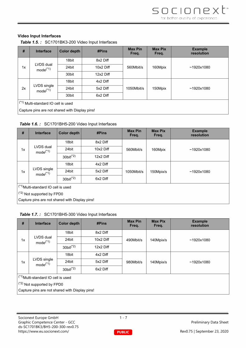
Video Input Interfaces
Table 1.5. : SC1701BK3-200 Video Input Interfaces
# Interface Color depth #PinsMax Pin
Freq.Max Pix
Freq.Example
resolution
1xLVDS dual
mode(*1)
18bit 8x2 Diff
560Mbit/s 160Mpix ~1920x108024bit 10x2 Diff
30bit 12x2 Diff
2xLVDS single
mode(*1)
18bit 4x2 Diff
1050Mbit/s 150Mpix ~1920x108024bit 5x2 Diff
30bit 6x2 Diff
(*1) Multi-standard IO cell is used
Capture pins are not shared with Display pins!
Table 1.6. : SC1701BH5-200 Video Input Interfaces
# Interface Color depth #Pins Max Pin Freq.
Max Pix Freq.
Exampleresolution
1xLVDS dual
mode(*1)
18bit 8x2 Diff
560Mbit/s 160Mpix ~1920x108024bit 10x2 Diff
30bit(*2) 12x2 Diff
1xLVDS single
mode(*1)
18bit 4x2 Diff
1050Mbit/s 150Mpix/s ~1920x108024bit 5x2 Diff
30bit(*2) 6x2 Diff
(*1)Multi-standard IO cell is used
(*2) Not supported by FPD0
Capture pins are not shared with Display pins!
Table 1.7. : SC1701BH5-300 Video Input Interfaces
# Interface Color depth #PinsMax Pin
Freq.Max Pix
Freq.Example
resolution
1xLVDS dual
mode(*1)
18bit 8x2 Diff
490Mbit/s 140Mpix/s ~1920x108024bit 10x2 Diff
30bit(*2) 12x2 Diff
1xLVDS single
mode(*1)
18bit 4x2 Diff
980Mbit/s 140Mpix/s ~1920x108024bit 5x2 Diff
30bit(*2) 6x2 Diff
(*1)Multi-standard IO cell is used
(*2) Not supported by FPD0
Capture pins are not shared with Display pins!
Socionext Europe GmbH 1 - 7Graphic Competence Center - GCC Preliminary Data Sheetds-SC1701BK3/BH5-200-300-rev0.75https://www.eu.socionext.com/ Rev0.75 | September 23, 2020PUBLIC
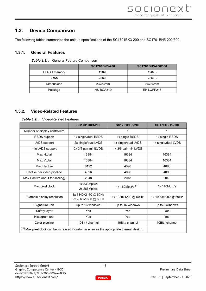
1.3. Device Comparison
The following tables summarize the unique specifications of the SC1701BK3-200 and SC1701BH5-200/300.
1.3.1. General Features
1.3.2. Video-Related Features
Table 1.8. : General Feature Comparison
SC1701BK3-200 SC1701BH5-200/300
FLASH memory 128kB 128kB
SRAM 256kB 256kB
Dimensions 23x23mm 24x24mm
Package HS-BGA319 EP-LQFP216
Table 1.9. : Video-Related Features
SC1701BK3-200 SC1701BH5-200 SC1701BH5-300
Number of display controllers 2 1 1
RSDS support 1x single/dual RSDS 1x single RSDS 1x single RSDS
LVDS support 2x single/dual LVDS 1x single/dual LVDS 1x single/dual LVDS
miniLVDS support 2x 3/6 pair miniLVDS 1x 3/6 pair miniLVDS -
Max Htotal 16384 16384 16384
Max Vtotal 16384 16384 16384
Max Hactive 8192 4096 4096
Hactive per video pipeline 4096 4096 4096
Max Hactive (input for scaling) 2048 2048 2048
Max pixel clock1x 533Mpix/s
2x 266Mpix/s1x 160Mpix/s (*1) 1x 140Mpix/s
Example display resolution1x 3840x2160 @ 60Hz
2x 2560x1600 @ 60Hz1x 1920x1200 @ 60Hz 1x 1920x1080 @ 60Hz
Signature unit up to 16 windows up to 16 windows up to 8 windows
Safety layer Yes Yes Yes
Histogram unit Yes Yes Yes
Color pipeline 10Bit / channel 10Bit / channel 10Bit / channel
(*1) Max pixel clock can be increased if customer ensures the appropriate thermal design.
Socionext Europe GmbH 1 - 8Graphic Competence Center - GCC Preliminary Data Sheetds-SC1701BK3/BH5-200-300-rev0.75https://www.eu.socionext.com/ Rev0.75 | September 23, 2020PUBLIC

1.4. Block Diagrams
1.4.1. SC1701BK3-200 Overview Block Diagram
Figure 1.1. : SC1701BK3-200 block diagram
Memory
128kB Flash 256kB SRAM(9kB with ECC)
Command Sequencer
System
Watchdog Clock
Config. FiFoTimer
CaptureEngine
SEERIS™ 2D Engine
4 planes, 34 layers, Alpha blend, Up/down-scale, Safety layerSignature Unit
LVDS, istogram
PixelEngine
ADC
Connectivity
PWM
HS-SPISPI Master
GPIO
UARTUSART/LIN
CAN
SMC
Connectivity
I2C
Ext. Serial Flash I/F
HOST I/F
I2S
Interrupt
Dithering, CLUT, Dual TCONDual output: 2x266Mpix/s, 4k/30bit
LVDS/OpenLDI, miniLVDS, TTL, RSDS
DisplayOutputEngine
SC1701 K3-200
Temperature Sensor
Socionext Europe GmbH 1 - 9Graphic Competence Center - GCC Preliminary Data Sheetds-SC1701BK3/BH5-200-300-rev0.75https://www.eu.socionext.com/ Rev0.75 | September 23, 2020PUBLIC

1.4.2. SC1701BH5-200 Overview Block Diagram
Figure 1.2. : SC1701BH5-200 block diagram
Memory
128kB Flash 256kB SRAM(9kB with ECC)
CaptureEngine
SEERIS™ 2D Engine
4 planes, 34 layers, Alpha blend, Up/down-scale, Safety layerSignature Unit
LVDS, istogram
PixelEngine
ADC
Connectivity
PWM
HS-SPISPI Master
GPIO
UARTUSART/LIN
CAN
SMC
Connectivity
I2C
Ext. Serial Flash I/F
HOST I/F
I2S
Interrupt
Dithering, CLUT, TCONOutput: 160Mpix/s, FHD/30bit
LVDS/OpenLDI, miniLVDS, TTL, RSDS
DisplayOutputEngine
SC1701 H5-200
Command Sequencer
System
Watchdog Clock
Config. FiFoTimer
Temperature Sensor
Socionext Europe GmbH 1 - 10Graphic Competence Center - GCC Preliminary Data Sheetds-SC1701BK3/BH5-200-300-rev0.75https://www.eu.socionext.com/ Rev0.75 | September 23, 2020PUBLIC

1.4.3. SC1701BH5-300 Overview Block Diagram
Figure 1.3. : SC1701BH5-300 block diagram
Memory
128kB Flash 256kB SRAM(9kB with ECC)
CaptureEngine
SEERIS™ 2D Engine
4 planes, 34 layers, Alpha blend, Safety layerSignature Unit
LVDS,Histogram
PixelEngine
ADC
Connectivity
PWM
HS-SPISPI Master
GPIO
UARTUSART/LIN
CAN
SMC
Connectivity
I2C
Ext. Serial Flash I/F
HOST I/F
I2S
Interrupt
Dithering, CLUT, TCONOutput: 140Mpix/s, FHD/30bit
LVDS/OpenLDI, TTL, RSDS
DisplayOutputEngine
SC1701BH5-300
Command Sequencer
System
Watchdog Clock
Config. FiFoTimer
Temperature Sensor
Socionext Europe GmbH 1 - 11Graphic Competence Center - GCC Preliminary Data Sheetds-SC1701BK3/BH5-200-300-rev0.75https://www.eu.socionext.com/ Rev0.75 | September 23, 2020PUBLIC

1.5. Package
1.5.1. SC1701BK3-200 Package
Figure 1.4. : SC1701BK3-200 Package
Table 1.10. : Package Characteristics
Package HS-BGA
Pins 319
Dimensions 23 x 23 mm
Pitch 1 mm
���� ��� ��� ������������
Socionext Europe GmbH 1 - 12Graphic Competence Center - GCC Preliminary Data Sheetds-SC1701BK3/BH5-200-300-rev0.75https://www.eu.socionext.com/ Rev0.75 | September 23, 2020PUBLIC

1.5.2. SC1701BH5-200/300 Package
Figure 1.5. : SC1701BH5-200/300 Package (top view, dimensions in mm)
Table 1.11. : Package Characteristics
Package EP-LQFP
Pins 216
Dimensions 24x24 mm
Pitch 0.4 mm
Socionext Europe GmbH 1 - 13Graphic Competence Center - GCC Preliminary Data Sheetds-SC1701BK3/BH5-200-300-rev0.75https://www.eu.socionext.com/ Rev0.75 | September 23, 2020PUBLIC

Figure 1.6. : SC1701BH5-200/300 Package (bottom view; dimensions in mm)
Figure 1.7. : SC1701BH5-200/300 - Exposed pad soldering pattern
26.4mm 24mm
6.0mm
6.0m
m
1.2m
m
0.4mm
a
0.19mm a 0.24mm
1.275mm
1.275mm
0.3mm
A
B
A
B
Socionext Europe GmbH 1 - 14Graphic Competence Center - GCC Preliminary Data Sheetds-SC1701BK3/BH5-200-300-rev0.75https://www.eu.socionext.com/ Rev0.75 | September 23, 2020PUBLIC

1.6. Part Number Code
Figure 1.8. : Part number code
XX #### % - ***
Unique IdentifierSC= Socionext
Chip Code####= 1701
VersionA= ES1
B= ES2 / CS
Option Code100 10N200300
Package CodeK3= HS-BGAH5= EP-LQFP
XX
Socionext Europe GmbH 1 - 15Graphic Competence Center - GCC Preliminary Data Sheetds-SC1701BK3/BH5-200-300-rev0.75https://www.eu.socionext.com/ Rev0.75 | September 23, 2020PUBLIC

1.7. Pinning
1.7.1. SC1701BK3-200 Pin Overview
Figure 1.9. : SC1701BK3-200 Pin Overview
1 2 3 4 5 6 7 8 9 10 11 12 13 14 15 16 17 18 19 20 21 22
TOP VIEW
A #VSS1 TSIG0_5
TSIG0_2 TMS #VSS8
9SMC_2
M_3SMC_1
M_3SMC_2
M_2SMC_1
M_2SMC_2
M_1SMC_1
M_1SMC_2
M_0SMC_1
M_0#VSS8
7 ADC0 ADC2 ADC6 #VSS84
TSIG1_0
TSIG1_2
TSIG1_5 #VSS4 A
B TSIG0_7
TSIG0_6
TSIG0_4
TSIG0_1
#VSS90
SMC_2P_3
SMC_1P_3
SMC_2P_2
SMC_1P_2
SMC_2P_1
SMC_1P_1
SMC_2P_0
SMC_1P_0
#VSS88 ADC1 ADC3 ADC7 #VSS8
5TSIG1
_1TSIG1
_4TSIG1
_6TSIG1
_8 B
C #VSS26
#VSS27
#VSS28
TSIG0_3
TSIG0_0 TCK TDI TRST #VSS9
1#VSS9
2#VSS9
3#VSS9
4FLSH_
TMFLSH_VREF
#VSS86 ADC4 ADC5 FSOU
RCETSIG1
_3#VSS7
8#VSS8
2#VSS8
3 C
D DISP0P15
DISP0N15
#VSS29
TSIG0_8
#VDDE16 TDO #VSS9
5#VDDE
24#VDDE
23#VDDE
22#VSS9
6#VSS9
7#VSS9
8#VDDE
21ADC_AVD
RESETO_N
RESET_N
#VDDE20
TSIG1_7
#VSS79
DISP1N15
DISP1P15 D
E DISP0P14
DISP0N14
#VDDE1
TSIG0_9
TSIG1_9
#VSS80
DISP1N14
DISP1P14 E
F DISP0P13
DISP0N13
#VSS30
TSIG0_10
TSIG1_10
#VSS81
DISP1N13
DISP1P13 F
G DISP0P12
DISP0N12
#VDDE2
TSIG0_11
TSIG1_11
#VDDE19
DISP1N12
DISP1P12 G
H DISP0P11
DISP0N11
#VSS31
#VDDE3
#VSS73
#VSS64
DISP1N11
DISP1P11 H
J DISP0P10
DISP0N10
#VSS32
#VDDE4 #VSS5 #VDDI
1#VDDI
2#VDDI
3#VDDI
4#VSS2
5#VDDE
18#VSS6
5DISP1N10
DISP1P10 J
K DISP0P9
DISP0N9
#VDDE5
#VSS58
#VDDI5 #VSS6 #VSS1
0#VSS1
5#VSS2
0#VDDI
11#VDDE
17#VSS6
6DISP1
N9DISP1
P9 K
L DISP0P8
DISP0N8
#VSS33
#VSSEPLL0
#VDDI6 #VSS7 #VSS1
1#VSS1
6#VSS2
1#VDDI
12#VSSEPLL1
#VSS67
DISP1N8
DISP1P8 L
M DISP0P7
DISP0N7
#VSS34
#VDDEPLL0
#VDDI7 #VSS8 #VSS1
2#VSS1
7#VSS2
2#VDDI
13#VDDEPLL1
#VSS68
DISP1N7
DISP1P7 M
N DISP0P6
DISP0N6
#VSS35
#VDDE6
#VDDI8 #VSS9 #VSS1
3#VSS1
8#VSS2
3#VDDI
14#VDDE
15#VSS6
9DISP1
N6DISP1
P6 N
P DISP0P5
DISP0N5
#VSS36
#VSS60
#VDDI9
#VDDI10
#VSSA2
#VSSA3
#VSS24
#VDDI15
#VSS75
#VSS70
DISP1N5
DISP1P5 P
R DISP0P4
DISP0N4
#VSS37
#VSS61
#VSS76
#VSS71
DISP1N4
DISP1P4 R
T DISP0P3
DISP0N3
#VSS38
#VSS62
#VSS77
#VSS72
DISP1N3
DISP1P3 T
U DISP0P2
DISP0N2
#VDDE7
#VSS63 GPIO7 #VDDE
14DISP1
N2DISP1
P2 U
V DISP0P1
DISP0N1
#VDDE8 GPIO0 N #VSSA
1 N GPIO6 #VDDE13
DISP1N1
DISP1P1 V
W DISP0P0
DISP0N0
#VSS39 GPIO1 GPIO2 I2C0_S
DAI2C0_S
CL#VDDE
10#VSS4
7#VDEA
2#VDEA
3TEST_
EN GPIO8 GPIO3 GPIO4 #VSS57
DISP1N0
DISP1P0 W
Y #VSS40
#VSS41
#VSS42
#VSS43
#VSS44
#VSS45
#VDDE9
#VSS48
#VSS49
#VDEA1
#VDDA_VCO1
#VSSA7
#VSSA8
#VSS51
#VSS52
#VSS53
#VDDE12 GPIO5 #VSS5
4#VSS5
5 Y
AA #VSS46
FPD0_N4
FPD0_N3
FPD0_NCK
FPD0_N2
FPD0_N1
FPD0_N0
#VDDE11 XO #VSSA
4#VSSA
6#VDDA
2#VDDA
4FPD1_
N0FPD1_
N1FPD1_
N2FPD1_NCK
FPD1_N3
FPD1_N4
#VSS56 AA
AB #VSS2 FPD0_P4
FPD0_P3
FPD0_PCK
FPD0_P2
FPD0_P1
FPD0_P0
#VSS50 XI #VDDA
1#VDDA
3 ATST #VSSA5
FPD1_P0
FPD1_P1
FPD1_P2
FPD1_PCK
FPD1_P3
FPD1_P4 #VSS3 AB
1 2 3 4 5 6 7 8 9 10 11 12 13 14 15 16 17 18 19 20 21 22
Socionext Europe GmbH 1 - 16Graphic Competence Center - GCC Preliminary Data Sheetds-SC1701BK3/BH5-200-300-rev0.75https://www.eu.socionext.com/ Rev0.75 | September 23, 2020PUBLIC

1.7.2. SC1701BH5-200/300 Pin Overview
Figure 1.10. : SC1701BH5-200/300 Pin Overview (multiplex functionality). See attached fi le pinout_QFP216_X_v1.22.xlsx for a detailed view.
1.7.3. Pin Descriptions and Multiplexing
The functionality of many pins changes according to the pin multiplexing mode that is set.
SC1701BK3-200: For details refer to the attached pin table SC1701BK3-200_pinlist_v1.22.xlsx.
SC1701BH5-200: For details refer to the attached pin table SC1701BH5-200_pinlist_v1.22.xlsx.
SC1701BH5-300: For details refer to the attached pin table SC1701BH5-300_pinlist_v1.23.xlsx.
TM TM TM TM
EIR
Q_7
EIR
Q_6
NO
T_U
SED
7N
OT_
USE
D7
NO
T_U
SED
7
EXTM
AC_R
MII_
CLK
EXTM
AC_R
MII_
RX_
DV
EXTM
AC_R
MII_
RXD
1EX
TMAC
_RM
II_R
XD0
EXTM
AC_R
MII_
RX_
ERH
OST
_IN
T0EX
TMAC
_RM
II_TX
D1
EXTM
AC_R
MII_
TXD
0EX
TMAC
_RM
II_TX
_EN
EXTP
HY
MII
RXC
LKR
E
CAN
_TX
CAN
_RX
NO
T_U
SED
7N
OT_
USE
D7
NO
T_U
SED
7N
OT_
USE
D7
ADC
0AD
C1
ADC
2AD
C3
ADC
5AD
C6
NO
T_U
SED
7N
OT_
USE
D7
NO
T_U
SED
7N
OT_
USE
D7
NO
T_U
SED
7N
OT_
USE
D7
NO
T_U
SED
7N
OT_
USE
D7
HO
ST_I
NT0
CAN
_TX
CAN
_RX
CAN
_TX
CAN
_RX
EXTM
AC_M
II_R
X_C
LKEX
TMAC
_MII_
RX_
DV
EXTM
AC_M
II_R
XD3
EXTM
AC_M
II_R
XD2
EXTM
AC_M
II_R
XD1
EXTM
AC_M
II_R
XD0
EXTM
AC_M
II_TX
_CLK
EXTM
AC_M
II_TX
_EN
EXTM
AC_M
II_TX
D3
EXTM
AC_M
II_TX
D2
EXTM
AC_M
II_TX
D1
EXTM
AC_M
II_TX
D0
EXTM
AC_M
II_R
X_ER
NO
T_U
SED
CAN
_TX
CAN
_RX
ADC
0AD
C1
ADC
2AD
C3
ADC
5AD
C6
CAN
_TX
CAN
_RX
NO
T_U
SED
CAN
_TX
CAN
_RX
NO
T_U
SED
CAN
_TX
CAN
_RX
SPI3
_SD
I
SPI3
_SC
LKSP
I3_S
DO
USA
RT1
_DO
USA
RT1
_DI
EXTP
HY_
MII_
TXC
LKEX
TPH
Y_M
II_TX
_EN
EXTP
HY_
MII_
TXD
3EX
TPH
Y_M
II_TX
D2
EXTP
HY_
MII_
TXD
1EX
TPH
Y_M
II_TX
D0
EXTP
HY
MII
RXC
LKR
EXTP
HY_
MII_
RX_
DV
EXTP
HY_
MII_
RXD
3EX
TPH
Y_M
II_R
XD2
EXTP
HY_
MII_
RXD
1EX
TPH
Y_M
II_R
XD0
EXTP
HY_
MII_
RX_
ERU
SAR
T1_D
OEI
RQ
_0EI
RQ
_1
ADC
0AD
C1
ADC
2AD
C3
ADC
5AD
C6
SPI_
CLK
SPI_
SDIO
0SP
I_SD
IO1
SPI_
SDIO
2SP
I_SD
IO3
SPI_
CS3
SPI_
CS2
SPI_
CS1
USA
RT0
D
HO
ST_I
NT0
EIR
Q_5
EIR
Q_1
EIR
Q_0
FLSH
SDIO
FLSH
SDIO
FLSH
SDIO
FLSH
SDIO
FLSH
_CLK
FLSH
_CS0
FLSH
_CS1
FLSH
_CS2
FLSH
_CS3
EIR
Q_6
USA
RT1
DU
SAR
T1C
USA
RT1
_DI
USA
RT0
CU
SAR
T0D
USA
RT0
_DI
ADC
0AD
C1
ADC
2AD
C3
ADC
5AD
C6
SPI0
_SC
LKSP
I0_S
DO
SPI0
_SD
ISP
I1_S
CLK
SPI1
_SD
ISP
I1_S
DO
EIR
Q_2
EIR
Q_3
PPG
_7B
PPG
_4B
PPG
_5B
HO
ST_I
NT0
PPG
_14B
PPG
_7B
PPG
_4B
EXTP
HY
REX
TPH
YR
EXTP
HY
REX
TPH
YR
EXTP
HY
REX
TPH
YR
EXTP
HY
REX
TPH
YR
PPG
_5B
PPG
_2B
PPG
_3B
PPG
_0B
PPG
_1B
PPG
_14B
ADC
0AD
C1
ADC
2AD
C3
ADC
5AD
C6
PPG
_15B
PPG
_12B
PPG
_13B
PPG
_10B
PPG
_11B
PPG
_8B
PPG
_9B
PPG
_6B
PPG
_6
PPG
_5PP
G_4
PPG
_0PP
G_1
5
PPG
_14
PPG
_13
PPG
_12
PPG
_11
PPG
_10
PPG
_9PP
G_8
PPG
_7PP
G_6
PPG
_5
PPG
_4PP
G_3
PPG
_2PP
G_1
PPG
_0PP
G_1
5
ADC
0AD
C1
ADC
2AD
C3
ADC
5AD
C6
PPG
_14
PPG
_13
PPG
_12
PPG
_11
PPG
_10
PPG
_9PP
G_8
PPG
_7
TSIG
0_7
TSIG
0_6
TSIG
0_5
TSIG
0_1
TSIG
0_0
SMC
_2P_
3SM
C_2
M_3
SMC
_1P_
3SM
C_1
M_3
SMC
_2P_
2SM
C_2
M_2
SMC
_1P_
2SM
C_1
M_2
SMC
_2P_
1SM
C_2
M_1
SMC
_1P_
1SM
C_1
M_1
SMC
_2P_
0SM
C_2
M_0
SMC
_1P_
0SM
C_1
M_0
ADC
0AD
C1
ADC
2AD
C3
ADC
5AD
C6
TSIG
1_0
TSIG
1_1
TSIG
1_2
TSIG
1_3
TSIG
1_4
TSIG
1_5
TSIG
1_6
TSIG
1_7
GPI
O10
2
GPI
O10
1G
PIO
100
GPI
O96
GPI
O95
HO
ST_D
OH
OST
_XC
S
HO
ST_S
CK
HO
ST_D
ITR
STG
PIO
94G
PIO
93G
PIO
92G
PIO
91
GPI
O90
GPI
O89
GPI
O88
GPI
O87
GPI
O86
GPI
O85
GPI
O84
GPI
O83
GPI
O82
GPI
O81
GPI
O80
GPI
O79
FLSH
_VR
EF
ADC
0AD
C1
ADC
2AD
C3
ADC
5AD
C6
RES
ETO
_NR
ESET
_N
GPI
O78
GPI
O77
GPI
O76
GPI
O75
GPI
O74
GPI
O73
GPI
O72
GPI
O71
VSS
TSIG
VDE
TSIG
TSIG
TSIG
TSIG
SYST
EMSY
STEM
VDD
SYST
EMSY
STEM
SYST
EMSM
CSM
CSM
CSM
CVD
DSM
CSM
CSM
CSM
CSM
CSM
CVD
DSM
CSM
CSM
CSM
CSM
CSM
CVD
DFL
SH_V
REF
ADC
_AVD
ADC
ADC
ADC
ADC
ADC
ADC
VDD
SYST
EMSY
STEM
VDE
TSIG
TSIG
TSIG
TSIG
TSIG
TSIG
TSIG
TSIG
VDE
VSS
216
215
214
213
212
211
210
209
208
207
206
205
204
203
202
201
200
199
198
197
196
195
194
193
192
191
190
189
188
187
186
185
184
183
182
181
180
179
178
177
176
175
174
173
172
171
170
169
168
167
166
165
164
163
VSS 1 162 VSSSPI3 SDI EXTMAC RMII TXD0 EIRQ 4 USART0 CLK PPG 6B PPG 7 TSIG0 8 GPIO103 TSIG 2 161 TSIG GPIO70 TSIG1 8 PPG 6 PPG 7B SPI0 SCLK SPI CS0 NOT USED NOT USED7NOT USED7 EXTMAC RMII TXD1 EIRQ 5 USART0 DI PPG 9B PPG 8 TSIG0 9 GPIO104 TSIG 3 160 TSIG GPIO69 TSIG1 9 PPG 5 PPG 4B SPI0 SDO EIRQ 5 NOT USED NOT USED7CAN RX EXTMAC RMII TX E I2C1 SCL SG SGA PPG 8B PPG 9 TSIG0 10 GPIO105 TSIG 4 159 TSIG GPIO68 TSIG1 10 PPG 4 PPG 5B SPI0 SDI EIRQ 6 NOT USED NOT USED7CAN TX EXTMAC RMII CLK I2C1 SDA SG SGO PPG 11B PPG 10 TSIG0 11 GPIO106 TSIG 5 158 TSIG GPIO67 TSIG1 11 PPG 3 PPG 2B SPI1 SCLK EIRQ 7 NOT USED NOT USED7
VDD 6 157 VDDCAN RX EXTMAC RMII RX E TSIG0 0 USART1 DO PPG 10B PPG 11 DISP0P15 GPIO107 DISP0 7 156 DISP1 GPIO66 DISP1P15 PPG 2 PPG 3B SPI1 SDO TSIG1 0 NOT USED NOT USED7CAN TX EXTMAC RMII RX D TSIG0 1 USART1 DI PPG 13B PPG 12 DISP0N15 GPIO108 DISP0 8 155 DISP1 GPIO65 DISP1N15 PPG 1 PPG 0B SPI1 SDI TSIG1 1 NOT USED NOT USED7
VDE 9 154 VDEHOST INT0 EXTMAC RMII RXD0 TSIG0 2 USART0 DO PPG 12B PPG 13 DISP0P14 GPIO109 DISP0 10 153 DISP1 GPIO64 DISP1P14 PPG 0 PPG 1B SPI3 SCLK TSIG1 2 NOT USED NOT USED7EXTPHY MII RXCLK EXTMAC RMII RXD1 TSIG0 3 USART0 DI PPG 15B PPG 14 DISP0N14 GPIO110 DISP0 11 152 DISP1 GPIO63 DISP1N14 PPG 15 PPG 14B SPI3 SDO TSIG1 3 NOT USED NOT USED7
VDD 12 151 VDDEXTPHY RMII TXD0 EXTMAC MII TXD0 EXTPHY MII I2S SD PPG 14B PPG 15 DISP0P13 GPIO111 DISP0 13 150 DISP1 GPIO62 DISP1P13 PPG 14 PPG 15B SPI3 SDI TSIG1 4 NOT USED NOT USED7EXTPHY RMII TXD1 EXTMAC MII TXD1 EXTPHY MII I2S SCLK PPG 1B PPG 0 DISP0N13 GPIO112 DISP0 14 149 DISP1 GPIO61 DISP1N13 PPG 13 PPG 12B SPI2 SCLK TSIG1 5 NOT USED NOT USED7EXTPHY RMII TX ENEXTMAC MII TXD2 EXTPHY MII NOT USED4 PPG 0B PPG 1 DISP0P12 GPIO113 DISP0 15 148 DISP1 GPIO60 DISP1P12 PPG 12 PPG 13B SPI2 SDO TSIG1 6 NOT USED NOT USED7EXTPHY RMII CLK EXTMAC MII TXD3 EXTPHY MII I2S WS PPG 3B PPG 2 DISP0N12 GPIO114 DISP0 16 147 DISP1 GPIO59 DISP1N12 PPG 11 PPG 10B SPI2 SDI TSIG1 7 NOT USED NOT USED7EXTPHY RMII RX E EXTMAC MII TX EN EXTPHY MII FPD0 P4 PPG 2B PPG 3 DISP0P11 GPIO115 DISP0 17 146 DISP1 GPIO58 DISP1P11 PPG 10 PPG 11B SPI CLK NOT USED5 NOT USED NOT USED7EXTPHY RMII RX D EXTMAC MII TX CL EXTPHY MII FPD0 N4 PPG 5B PPG 4 DISP0N11 GPIO116 DISP0 18 145 DISP1 GPIO57 DISP1N11 PPG 9 PPG 8B SPI SDIO0 NOT USED5 NOT USED NOT USED7
VDD 19 144 VDDEXTPHY RMII RXD0 EXTMAC MII RXD0 EXTPHY MII FPD0 P3 PPG 4B PPG 5 DISP0P10 GPIO117 DISP0 20 143 DISP1 GPIO56 DISP1P10 PPG 8 PPG 9B SPI SDIO1 NOT USED5 NOT USED NOT USED7EXTPHY RMII RXD1 EXTMAC MII RXD1 EXTPHY MII FPD0 N3 PPG 7B PPG 6 DISP0N10 GPIO118 DISP0 21 142 DISP1 GPIO55 DISP1N10 PPG 7 PPG 6B SPI SDIO2 NOT USED5 NOT USED NOT USED7EXTMAC RMII TXD0 EXTMAC MII RXD2 EXTPHY MII FPD0 PCK PPG 6B PPG 7 DISP0P9 GPIO119 DISP0 22 141 DISP1 GPIO54 DISP1P9 PPG 6 PPG 7B SPI SDIO3 NOT USED5 NOT USED NOT USED7EXTMAC RMII TXD1 EXTMAC MII RXD3 EXTPHY MII FPD0 NCK PPG 9B PPG 8 DISP0N9 GPIO120 DISP0 23 140 DISP1 GPIO53 DISP1N9 PPG 5 PPG 4B SPI CS3 NOT USED5 NOT USED NOT USED7EXTMAC RMII TX E EXTMAC MII RX DV EXTPHY MII FPD0 P2 PPG 8B PPG 9 DISP0P8 GPIO121 DISP0 24 139 DISP1 GPIO52 DISP1P8 PPG 4 PPG 5B SPI CS2 NOT USED5 NOT USED NOT USED7EXTMAC RMII CLK EXTMAC MII RX CL EXTPHY MII FPD0 N2 PPG 11B PPG 10 DISP0N8 GPIO122 DISP0 25 138 DISP1 GPIO51 DISP1N8 PPG 3 PPG 2B SPI CS1 NOT USED5 NOT USED NOT USED7
VDD 26 137 VDDEXTMAC RMII RX E EXTMAC MII RX ER EIRQ 3 FPD0 P1 PPG 10B PPG 11 DISP0P7 GPIO123 DISP0 27 136 DISP1 GPIO50 DISP1P7 PPG 2 PPG 3B SPI CS0 NOT USED5 NOT USED NOT USED7EXTMAC RMII RX D EIRQ 2 EXTPHY MII FPD0 N1 PPG 13B PPG 12 DISP0N7 GPIO124 DISP0 28 135 DISP1 GPIO49 DISP1N7 PPG 1 PPG 0B NOT USED4 SPI0 SDI NOT USED EXTMAC RMII RX DVEXTMAC RMII RXD0 NOT USED EIRQ 1 FPD0 P0 PPG 12B PPG 13 DISP0P6 GPIO125 DISP0 29 134 DISP1 GPIO48 DISP1P6 PPG 0 PPG 1B NOT USED4 SPI0 SCLK NOT USED EXTMAC RMII RXD1EXTMAC RMII RXD1 NOT USED EIRQ 0 FPD0 N0 PPG 15B PPG 14 DISP0N6 GPIO126 DISP0 30 133 DISP1 GPIO47 DISP1N6 PPG 15 PPG 14B NOT USED4 SPI0 SDO EXTMAC MII RX ER EXTMAC RMII RXD0
VDE 31 132 VDEVDD 32 131 VDD
NOT USED7 NOT USED USART1 DI FPD1 P4 I2C1 SCL PPG 15 DISP0P5 GPIO127 DISP0 33 130 DISP1 GPIO46 DISP1P5 PPG 14 PPG 15B EXTPHY MII TXCLK TSIG1 8 EXTMAC MII RX CLK EXTMAC RMII CLKNOT USED7 NOT USED USART1 DO FPD1 N4 I2C1 SDA PPG 0 DISP0N5 GPIO128 DISP0 34 129 DISP1 GPIO45 DISP1N5 PPG 13 PPG 12B EXTPHY MII TX EN TSIG1 9 EXTMAC MII RX DV EXTMAC RMII TX ENNOT USED7 NOT USED USART1 CLK FPD1 P3 PPG 0B PPG 1 DISP0P4 GPIO129 DISP0 35 128 DISP1 GPIO44 DISP1P4 PPG 12 PPG 13B EXTPHY MII TXD3 TSIG1 10 EXTMAC MII RXD3 EXTMAC RMII TXD1NOT USED7 NOT USED SPI CS3 FPD1 N3 PPG 3B PPG 2 DISP0N4 GPIO130 DISP0 36 127 DISP1 GPIO43 DISP1N4 PPG 11 PPG 10B EXTPHY MII TXD2 TSIG1 11 EXTMAC MII RXD2 EXTMAC RMII TXD0NOT USED7 NOT USED SPI CS2 FPD1 PCK PPG 2B PPG 3 DISP0P3 GPIO131 DISP0 37 126 DISP1 GPIO42 DISP1P3 PPG 10 FLSH CS EXTPHY MII TXD1 TSIG1 0 EXTMAC MII RXD1 EXTMAC RMII RX ERNOT USED7 NOT USED SPI CS1 FPD1 NCK PPG 5B PPG 4 DISP0N3 GPIO132 DISP0 38 125 DISP1 GPIO41 DISP1N3 PPG 9 FLSH CS EXTPHY MII TXD0 TSIG1 1 EXTMAC MII RXD0 EXTPHY RMII RX ER
VDD 39 124 VDDNOT USED7 NOT USED SPI SDIO3 FPD1 P2 PPG 4B PPG 5 DISP0P2 GPIO133 DISP0 40 123 DISP1 GPIO40 DISP1P2 PPG 8 FLSH SD EXTPHY MII RXCLK TSIG1 2 EXTMAC MII TX CLK EXTPHY RMII CLKNOT USED7 NOT USED SPI SDIO2 FPD1 N2 PPG 7B PPG 6 DISP0N2 GPIO134 DISP0 41 122 DISP1 GPIO39 DISP1N2 PPG 7 FLSH SD EXTPHY MII RX DV TSIG1 3 EXTMAC MII TX EN EXTPHY RMII TX ENNOT USED7 NOT USED SPI SDIO1 FPD1 P1 PPG 6B PPG 7 DISP0P1 GPIO135 DISP0 42 121 DISP1 GPIO38 DISP1P1 PPG 6 FLSH SD EXTPHY MII RXD3 TSIG1 4 EXTMAC MII TXD3 EXTPHY RMII TXD1NOT USED7 NOT USED SPI SDIO0 FPD1 N1 PPG 9B PPG 8 DISP0N1 GPIO136 DISP0 43 120 DISP1 GPIO37 DISP1N1 PPG 5 FLSH SD EXTPHY MII RXD2 TSIG1 5 EXTMAC MII TXD2 EXTPHY RMII TXD0NOT USED7 CAN RX SPI CS0 FPD1 P0 PPG 8B PPG 9 DISP0P0 GPIO137 DISP0 44 119 DISP1 GPIO36 DISP1P0 PPG 4 FLSH CS EXTPHY MII RXD1 TSIG1 6 EXTMAC MII TXD1 EXTPHY RMII RXD1NOT USED7 CAN TX SPI CLK FPD1 N0 PPG 11B PPG 10 DISP0N0 GPIO138 DISP0 45 118 DISP1 GPIO35 DISP1N0 PPG 3 FLSH CLKEXTPHY MII RXD0 TSIG1 7 EXTMAC MII TXD0 EXTPHY RMII RXD0
VDE 46 117 VDEVDD 47 116 VDD
NOT USED7 HOST INT0 USART0 DI SG SGA PPG 1B PPG 0 I2C1 SCL GPIO0 PERIPHERIE 48 115 PERIPHERIE GPIO7 NOT USEDPPG 7 FLSH CS EXTPHY MII RX ER TSIG1 8 NOT USED EXTPHY RMII RX DVEXTPHY RMII TXD0 EXTMAC MII RX ER USART0 DO SG SGO PPG 0B PPG 1 I2C1 SDA GPIO1 PERIPHERIE 49 114 PERIPHERIE GPIO6 NOT USEDPPG 6 PPG 7B FLSH CS2 TSIG1 9 NOT USED I2S WSEXTPHY RMII TXD1 EXTMAC MII RX ER USART0 CLK NOT USED4 PPG 3B PPG 2 HOST INT0 GPIO2 PERIPHERIE 50 113 PERIPHERIE GPIO5 NOT USEDPPG 5 PPG 4B SPI3 SCLK TSIG1 10 CAN TX I2S SCLK
VDE 51 CURRENT VERSION 112 PERIPHERIE GPIO4 NOT USEDPPG 4 PPG 5B SPI3 SDO TSIG1 11 CAN RX I2S SDEXTPHY RMII TX ENEXTMAC MII TX CL USART1 DI NOT USED4 PPG 8B PPG 9 I2C0 SDA GPIO9 PERIPHERIE 52 111 VDEEXTPHY RMII CLK EXTMAC MII TX EN USART1 DO NOT USED4 I2S WS PPG 10 I2C0 SCL GPIO10 PERIPHERIE 53 110 PERIPHERIE GPIO3 USART0 DPPG 3 PPG 2B SPI3 SDI TSIG1 0 HOST INT0 NOT USED7
VSS 54 109 VSS
55 56 57 58 59 60 61 62 63 64 65 66 67 68 69 70 71 72 73 74 75 76 77 78 79 80 81 82 83 84 85 86 87 88 89 90 91 92 93 94 95 96 97 98 99 100
101
102
103
104
105
106
107
108
VSS
CAP
0C
AP0
VDE
CAP
0C
AP0
VDD
CAP
0C
AP0
CAP
0C
AP0
VDE
CAP
0C
AP0
VDD
OSC
OSC
VDD
VDD
AVD
EAN
CN
CN
CN
CVD
EAN
CVD
DA
VCO
ATST
NC
NC
VDEA
NC
NC
VDEA
VDD
AVD
DC
AP1
CAP
1VD
EC
AP1
CAP
1C
AP1
CAP
1VD
DC
AP1
CAP
1VD
EC
AP1
CAP
1C
AP1
CAP
1VD
DSY
STEM
VSS
GPI
O13
GPI
O14
GPI
O15
GPI
O16
GPI
O17
GPI
O18
GPI
O19
GPI
O20
GPI
O21
GPI
O22
OSC
_XI
OSC
_XO
GPI
O23
GPI
O24
GPI
O25
GPI
O26
GPI
O27
GPI
O28
GPI
O29
GPI
O30
GPI
O31
GPI
O32
GPI
O33
GPI
O34
TEST
_EN
FPD
0_P3
FPD
0_N
3
FPD
0_PC
KFP
D0_
NC
K
FPD
0_P2
FPD
0_N
2FP
D0_
P1FP
D0_
N1
FPD
0_P0
FPD
0_N
0
FPD
1_N
0FP
D1_
P0
FPD
1_N
1FP
D1_
P1FP
D1_
N2
FPD
1_P2
FPD
1_N
CK
FPD
1_PC
K
FPD
1_N
3FP
D1_
P3FP
D1_
N4
FPD
1_P4
PPG
_13
PPG
_14
PPG
_15
PPG
_0
SPI1
_SD
ISP
I1_S
DO
SPI1
_SC
LKSP
I0_S
DI
SPI0
_SD
OSP
I0_S
CLK
PPG
_7PP
G_8
PPG
_9PP
G_1
0PP
G_1
1PP
G_1
2
PPG
_13
PPG
_14
PPG
_15
PPG
_0PP
G_1
PPG
_2
NO
T_U
SED
3I2
S_W
S
SMC
_1M
_4SM
C_1
P_4
SMC
_2M
_4SM
C_2
P_4
SMC
_1M
_5SM
C_1
P_5
SMC
_2M
_5SM
C_2
P_5
USA
RT0
_DI
USA
RT0
_DO
USA
RT1
_DI
USA
RT1
_DO
I2C
0_SD
AI2
C0_
SCL
USA
RT1
_DI
USA
RT1
_DO
I2C
1_SD
AI2
C1_
SCL
SG_S
GO
SG_S
GA
NO
TU
SEN
OT
USE
EXTP
HY
REX
TPH
YR
EXTP
HY
REX
TPH
YR
EXTP
HY
REX
TPH
YR
NO
TU
SEN
OT
USE
SPI2
_SD
ISP
I2_S
DO
SPI2
_SC
LKSP
I3_S
DI
SPI3
_SD
OSP
I3_S
CLK
TSIG
1_7
TSIG
1_6
TSIG
1_5
TSIG
1_4
TSIG
1_3
TSIG
1_2
NO
TU
SEN
OT
USE
NO
TU
SEN
OT
USE
NO
TU
SEN
OT
USE
NO
TU
SEN
OT
USE
SG_S
GA
SG_S
GO
I2C
0_SD
AI2
C0_
SCL
NO
TU
SEN
OT
USE
NO
TU
SEN
OT
USE
NO
TU
SEN
OT
USE
NO
TU
SEN
OT
USE
NO
TU
SEN
OT
USE
EXTM
AC_M
II_TX
D0
EXTM
AC_M
II_TX
D1
EXTM
AC_M
II_TX
D2
EXTM
AC_M
II_TX
D3
EXTM
AC_M
II_R
X_C
LKEX
TMAC
_MII_
RX_
DV
EXTM
AC_M
II_R
XD0
EXTM
AC_M
II_R
XD1
EXTM
AC_M
II_R
XD2
EXTM
AC_M
II_R
XD3
CAN
_RX
CAN
_TX
NO
T_U
SED
NO
T_U
SED
NO
T_U
SED
NO
T_U
SED
CAN
_RX
CAN
_TX
NO
T_U
SED
NO
T_U
SED
CAN
_RX
CAN
_TX
EXTP
HY_
RM
II_R
XD0
EXTP
HY_
RM
II_R
XD1
EXTM
AC_R
MII_
TXD
0EX
TMAC
_RM
II_TX
D1
EXTM
AC_R
MII_
TX_E
NEX
TMAC
_RM
II_C
LKEX
TMAC
_RM
II_R
X_ER
EXTM
AC_R
MII_
RX_
DV
EXTM
AC_R
MII_
RXD
0EX
TMAC
_RM
II_R
XD1
NO
T_U
SED
7N
OT_
USE
D7
NO
T_U
SED
7N
OT_
USE
D7
NO
T_U
SED
7N
OT_
USE
D7
NO
T_U
SED
7N
OT_
USE
D7
NO
T_U
SED
7I2
S_W
SI2
S_SC
LKI2
S_SD
1.22
SC1701BH5-200
Socionext Europe GmbH 1 - 17Graphic Competence Center - GCC Preliminary Data Sheetds-SC1701BK3/BH5-200-300-rev0.75https://www.eu.socionext.com/ Rev0.75 | September 23, 2020PUBLIC

2. Electrical Characteristics
2.1. Operating Conditions
2.1.1. Absolute Maximum Ratings
Note: Semiconductor devices can be permanently damaged by application of stress (voltage, current, temperature, etc.) in excess of the absolute maximum ratings. Do not exceed these ratings.
Note: • Applying stress exceeding the maximum ratings (voltage, current, temperature, etc.) may cause damage to semiconductor devices. Never exceed the ratings above.
• Never connect IC outputs or I/O pins directly, or connect them to VDD or VSS directly, otherwise thermal destruction of elements will result. This does not apply to pins designed to prevent signal collision.
• Provide ESD protection, such as grounding, when handling the product; otherwise externally charged electric charge flows inside the IC and discharges, which may result in damage to the circuit.
• Applying voltage higher than VDD or lower than VSS to I/O pins of CMOS IC, or applying voltage higher than the ratings between VDD and VSS may cause latch-up. The latch-up increases supply current, resulting in thermal destruction of elements. When handling the product, never exceed the maximum ratings.
Table 2.1. : Absolute Maximum Ratings
Parameter Symbol Min Max Unit Comment
Core supply VDD VSS -0.3 VSS+1.8 V
IO supply VDE VSS -0.3 VSS+4.0 V
VPLL DISP0 supply VDDEPLL0 VSS -0.3 VSS+4.0 VOnly in SC1701BK3
VPLL DISP1 supply VDDEPLL1 VSS -0.3 VSS+4.0 V
ADC and bandgap reference supply
ADC_AVD VSS -0.3 VSS+4.0 V
PLL supply VDEA VSS -0.3 VSS+4.0 V
PLL core supply VDDA VSS -0.3 VSS+1.8 V
PLL VCO supply VDDA_VCO VSS -0.3 VSS+1.8 V
Input voltage* VI VSS -0.3 VDE +0.3 V
OSC input voltage XI VSS -0.3 VDD +0.3 V
OSC output voltage XO VSS -0.3 VDD +0.3 V
Analog input voltage VIA VSS -0.3 ADC_AVD + 0.3 V < 4.0V
Output voltage VO VSS -0.3 VDE +0.3 V < 4.0V
Storage temperature TST -55 150 °C
Junction temperature Tj -40 150 °C
* Input voltage of BID33-IO and MSIO (RSDS, LVDS, miniLVDS)
Socionext Europe GmbH 2 - 1Graphic Competence Center - GCC Preliminary Data Sheetds-SC1701BK3/BH5-200-300-rev0.75https://www.eu.socionext.com/ Rev0.75 | September 23, 2020PUBLIC

2.1.2. Recommended Operating Conditions
Table 2.2. : Recommended Operating Conditions
Parameter Symbol Min Typ Max Unit Comment
Core supply VDD 1.20 1.26 1.32 V
IO supply VDE 3.0 3.3 3.6 VIncluding GPIOs,
MSIOs, embedded flash
VPLL DISP0 supply VDDEPLL0 3.0 3.3 3.6 VOnly in SC1701BK3
VPLL DISP1 supply VDDEPLL1 3.0 3.3 3.6 V
ADC and bandgap reference supply
ADC_AVD 3.0 3.3 3.6 VStable supply is needed for operation of embed-
ded flash, POR and ADC
PLL supply VDEA 3.0 3.3 3.6 V
PLL core supply VDDA 1.20 1.26 1.32 V
PLL VCO supply VDDA_VCO 1.20 1.26 1.32 V
Ambient temperature Ta -40 105 °C
Socionext Europe GmbH 2 - 2Graphic Competence Center - GCC Preliminary Data Sheetds-SC1701BK3/BH5-200-300-rev0.75https://www.eu.socionext.com/ Rev0.75 | September 23, 2020PUBLIC

2.2. Power Consumption
2.3. Thermal Design Considerations
Table 2.4 shows the estimated junction-to-ambient thermal resistance and junction-to-top-center-of-package thermal characterization. This thermal performance depends not only on the SC1701 package, but also on the characteristics of the PCB on which it is mounted.
PCB conditions: JEDEC PCB 4 layer 114.3x101.6x1.6mm, FloTHERM_JEDEC environment. The power consumption varies according to the application (i.e., depending on the use case).
Table 2.3. : Power Consumption (estimated values)
Parameter Symbol
Rating
Unit CommentMin Typ
Max SC1701BK3-200 SC1701BH5-200 SC1701BH5-300
Core supply IVDD 1.80 1.20 A
IO supply IVDE 0.70 0.46 ABH5: DISP1, CAP1 VPLL, and CAP0 VPLL all active
VPLL0 supply IVDDE_PLL0 70 N/A mABK3: Both DISP0 and CAP0 VPLL active
VPLL1 supply IVDDE_PLL1 70 N/A mABK3: Both DISP1 and CAP1 VPLL active
ADC and bandgap reference supply
IADC_AVD 4 4 mA
PLL analog supply IVDDA 185 185 mA
PLL supply IVDEA 51 51 mA
PLL VCO supply IVDA_VCO 7 7 mA
N/A: Will not be available in SC1701BH5 chips.
Table 2.4. : Thermal Parameters
Device Package ΘJA[ºC/W] ΨJT[ºC/W] Comment
SC1701BH5 EP-LQFP216 15.9 0.26
SC1701BK3 TEBGA319 15.5 5.29
Socionext Europe GmbH 2 - 3Graphic Competence Center - GCC Preliminary Data Sheetds-SC1701BK3/BH5-200-300-rev0.75https://www.eu.socionext.com/ Rev0.75 | September 23, 2020PUBLIC

2.4. Clock Input
Figure 2.1. : Clock Input
Table 2.5. : Clock Input Specifications
Parameter Symbol Min Typ Max Unit Comment
Crystal frequency X1 -100 ppm 30 +100 ppm MHz (*2)
External load
capacityC1, C2 10 pF
Value depends on crystal
Damping resistor Rd OhmIf needed, value
depends on crystal
Input amplitudeVIH_XI 0.8 * VDD V
VIL_XI 0.2 * VDD V
Figure of effort EF 1.0 (*1)
(*1) EF= f * C0.8 * R0.61 where
EF = figure of effort
f= frequency of oscillation
C= capacitive loading on XI and XO
R= crystal equivalent series resistance
Use the figure of effort equation (EF) to confirm that oscillation can be achieved at the target frequency for the spe-cific loading characteristics (ESR, C) of the crystal in your design.
Note that the lower the calculated EF number is, the higher is the margin for the oscillator. The target EF number should be lower than the stated maximum to obtain more margin, recommended is EF < 0.8.
(*2) The listed accuracy is enough for the operation of typical video interfaces. If other interfaces, e.g. MII, need higher accuracy, then derive the necessary accuracy from the related blocks.
Socionext Europe GmbH 2 - 4Graphic Competence Center - GCC Preliminary Data Sheetds-SC1701BK3/BH5-200-300-rev0.75https://www.eu.socionext.com/ Rev0.75 | September 23, 2020PUBLIC

2.5. Reset Timing
Figure 2.2. : Reset Timing
Table 2.6. : Timing Parameters Reset
Parameter Symbol Min Typ Max Unit Comment
Reset low time TRST 1.0 ms
Socionext Europe GmbH 2 - 5Graphic Competence Center - GCC Preliminary Data Sheetds-SC1701BK3/BH5-200-300-rev0.75https://www.eu.socionext.com/ Rev0.75 | September 23, 2020PUBLIC

2.6. Power-On Sequence
The figure below shows the power-On sequence and the groups of power supply that might be used, depending on the actual application.
VDD12 stands for the following supplies: VDD, VDDA, VDDA_VCO
VDDE stands for the following supplies: VDE, VDDE_PLL0, VDDE_PLL1, VDEA, ADC_AVD
Figure 2.3. : Power-On Sequence
Table 2.7. : Power-On Timing Parameters
Parameter Symbol Min Typ Max Unit Comment
Power rise time tPWR_R 0.05 30 ms
Power rise delay tPWR_D 0 1 s
Power slew rate 0.1 20 mV/us
Socionext Europe GmbH 2 - 6Graphic Competence Center - GCC Preliminary Data Sheetds-SC1701BK3/BH5-200-300-rev0.75https://www.eu.socionext.com/ Rev0.75 | September 23, 2020PUBLIC

2.7. Flash Memory Program / Erase Characteristics
Table 2.8. : Program/Erase time
ParameterValue1)
Unit RemarksMin Max
Sector erase time 16 20 ms
Word programming time 16 20 µs
1)Program/Erase cycle = Immediately after shipment
Table 2.9. : Program/Erase cycle and data retention time2)
Program/Erase cycle at each sector Data retention time
Min value Unit Min value Unit
1000 cycles 20 years
10000 cycles 10 years
2)These parameters are measured only for initial qualification.
Socionext Europe GmbH 2 - 7Graphic Competence Center - GCC Preliminary Data Sheetds-SC1701BK3/BH5-200-300-rev0.75https://www.eu.socionext.com/ Rev0.75 | September 23, 2020PUBLIC

2.8. ADC Sampling Time
The SC1701 has an embedded 12-bit successive approximation ADC with an internal integrated sampling and holding stage. The signal will charge the sampling capacitor first and then the voltage signal on the sampling capacitor will be evaluated by the 12-bit ADC. The time to charge the sampling capacitor to its final value, equal to the signal level, is a function of the internal and external capacitor and resistor values. To reduce the error caused by the limited settling time to an acceptable level, the sampling time should be chosen much larger than the time constant to charge the sampling capacitor. The sampling time can be set with the ADC TIMING.Tsample register field.
Figure 2.4. : ADC input signal
The minimum sampling time can be calculated with the following formula:
Example: When ADC_AVD = 3.3V (see Table 2.2 for ADC_AVD range).
For pins ADC0 ...ADC7
Note: The application requirements determine the ADC bit width and factor F can be derived from Table 2.10 .
Table 2.10. : Factor F
ADC bit width F
12 (default) 9.02
11 8.32
10 7.63
9 6.94
8 6.24
7 5.55
6 4.86
5 4.16
4 3.47
3 2.78
2 2.08
1 1.39
Rext ADC
SC1701
Usig
Cext *)
MUX
ADC0...7
*) The ADC inputs should be bypassed with a capacitor 0.01~0.1uF.For details see Application Note: SC1701xxx PCB Design Guideline
Tsample min F 46ns 0.0135nF Rext Rext CextnF + + =
Socionext Europe GmbH 2 - 8Graphic Competence Center - GCC Preliminary Data Sheetds-SC1701BK3/BH5-200-300-rev0.75https://www.eu.socionext.com/ Rev0.75 | September 23, 2020PUBLIC
With Rext = 0Ω
Limitation
Tsample always < 10μs
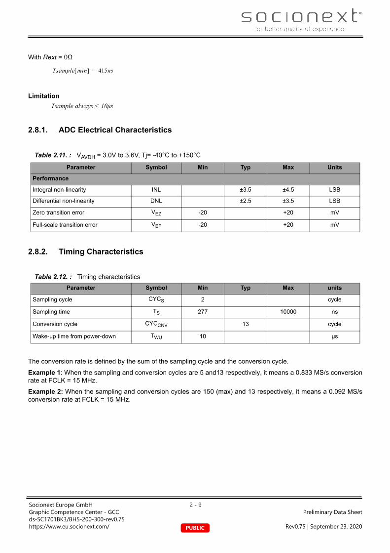
2.8.1. ADC Electrical Characteristics
2.8.2. Timing Characteristics
The conversion rate is defined by the sum of the sampling cycle and the conversion cycle.
Example 1: When the sampling and conversion cycles are 5 and13 respectively, it means a 0.833 MS/s conversion rate at FCLK = 15 MHz.
Example 2: When the sampling and conversion cycles are 150 (max) and 13 respectively, it means a 0.092 MS/s conversion rate at FCLK = 15 MHz.
Table 2.11. : VAVDH = 3.0V to 3.6V, Tj= -40°C to +150°C
Parameter Symbol Min Typ Max Units
Performance
Integral non-linearity INL ±3.5 ±4.5 LSB
Differential non-linearity DNL ±2.5 ±3.5 LSB
Zero transition error VEZ -20 +20 mV
Full-scale transition error VEF -20 +20 mV
Table 2.12. : Timing characteristics
Parameter Symbol Min Typ Max units
Sampling cycle CYCS 2 cycle
Sampling time TS 277 10000 ns
Conversion cycle CYCCNV 13 cycle
Wake-up time from power-down TWU 10 µs
Tsample min 415ns=
Socionext Europe GmbH 2 - 9Graphic Competence Center - GCC Preliminary Data Sheetds-SC1701BK3/BH5-200-300-rev0.75https://www.eu.socionext.com/ Rev0.75 | September 23, 2020PUBLIC

2.9. PCB Layout Recommendations
2.9.1. High Speed Interfaces
Please refer to the layout recommendations in Application Note “PCB Design Guideline”.
2.9.2. Configuration Pins
The following solutions are recommended when using the configuration pins.
Unused pin with pull-down
Figure 2.5. : Unused pin with pull-down
Unused pin with pull-up
Figure 2.6. : Unused pin with pull-up
After power On, the internal pull-down must be switched Off to avoid power leakage.
CFGx
Internal pull down resistancemin 35 kOhmtyp 60 kOhmmax 120 kOhm
open
CFGx
Internal pull down resistancemin 35 kOhmtyp 60 kOhmmax 120 kOhm
VDP3
External pull up resistance
Max 5.6 kOhm
Socionext Europe GmbH 2 - 10Graphic Competence Center - GCC Preliminary Data Sheetds-SC1701BK3/BH5-200-300-rev0.75https://www.eu.socionext.com/ Rev0.75 | September 23, 2020PUBLIC

Configuration pins are output - External device does not support pull-up
Figure 2.7. : Configuration pins are output
Note: The CFGx signal is latched 10us (260 osc_clk cycles after RESETN chip input released); therefore, disable CFG value driver 10us after chip reset release!
Configuration pins are input - External device does not support pull-up
Figure 2.8. : Configuration pins are input
In this case, we recommend implementing a tri-state buffer on the board and an additional tri-state buffer in order to disconnect the external device from the CFG signals. After power On, the internal pull-down should be disconnected.
Note: The CFGx signal is latched 10us (260 osc_clk cycles after RESETN chip input released); therefore, disable CFG value driver 10us after chip reset release!
CFGx
Internal pull down resistancemin 35 kOhmtyp 60 kOhmmax 120 kOhm
RESET_n
cfg value en
External device
CFGx
Internal pull down resistancemin 35 kOhmtyp 60 kOhmmax 120 kOhm
RESET_n
cfg value en
External device
en
Socionext Europe GmbH 2 - 11Graphic Competence Center - GCC Preliminary Data Sheetds-SC1701BK3/BH5-200-300-rev0.75https://www.eu.socionext.com/ Rev0.75 | September 23, 2020PUBLIC

IO - External device does not support pull-up
Figure 2.9. : IO - External device does not support pull-up
In this case, the external device must be in high-impedance state during reset. After power On, the internal pull-down should be disconnected.
Note: The CFGx signal is latched 10us (260 osc_clk cycles after RESETN chip input released); therefore, disable CFG value driver 10us after chip reset release!
CFGx
Internal pull down resistancemin 35 kOhmtyp 60 kOhmmax 120 kOhm
RESET_n
cfg value en
External device pinhas to be high ohmicduring reset
Socionext Europe GmbH 2 - 12Graphic Competence Center - GCC Preliminary Data Sheetds-SC1701BK3/BH5-200-300-rev0.75https://www.eu.socionext.com/ Rev0.75 | September 23, 2020PUBLIC

2.10. AC Limits
2.10.1. Host SPI Characteristics
2.10.1.1. Host SPI Interface
Figure 2.10. : Timing SPI interface
Table 2.13. : AC timing Host SPI interface
Parameter SymbolValue
Unit RemarksMin Typ Max
clk period tCK_HSPI 34 ns Minimum 4 * HCLK period.
clk to output data tCQ_HSPI 0 20 ns
Input data setup tSU_HSPI 10 ns
Input data hold tHD_HSPI 5 ns
Input Control setup tHD_TMS 50 + 2 * tHCLK ns
Input Control Hold tHD_TMS 50 + 2 * tHCLK ns
HOST_SCK
HOST_DO
tSU_HSPI tHD_HSPI
tCQ_HSPI(max) tCQ_HSPI(min)
HOST_DI
tCK_HSPI
HOST_XCS
tHD_TMStSU_TMS
Socionext Europe GmbH 2 - 13Graphic Competence Center - GCC Preliminary Data Sheetds-SC1701BK3/BH5-200-300-rev0.75https://www.eu.socionext.com/ Rev0.75 | September 23, 2020PUBLIC

2.10.2. Config Interface
Figure 2.11. : Timing configuration pins
Table 2.14. : AC timing configuration pins
Parameter SymbolValue
Unit RemarksMin Typ Max
cfg data setup tSU_CFG 50 ns
cfg data hold tHD_CFG 250 ns
tSU_CFG tHD_CFG
CFG
RESET_N
Socionext Europe GmbH 2 - 14Graphic Competence Center - GCC Preliminary Data Sheetds-SC1701BK3/BH5-200-300-rev0.75https://www.eu.socionext.com/ Rev0.75 | September 23, 2020PUBLIC

2.10.3. Display Interface
2.10.3.1. TTL Mode
Figure 2.12. : Timing display TTL interface
Table 2.15. : AC timing TTL display interface
Parameter SymbolValue
Unit RemarksMin Typ Max
dsp_clk period tDSP_CLK 5.5 ns Internal clock for reference only.
bit_clk period tBIT_CLK 1.8 nsInternal clock for reference only, integer multiple of dsp_clk.
Pixel clock period tPIX_CLK 11 11.7 ns
Typical value is maximum pixel frequency, minimum value is due to spread spectrum and clock synthesis.
Shift value tSS_DISP typ -150 typ + 150 ps
Half cycle shift tSH_DISP typ -200 typ + 200 ps
TTL DISP mismatch tM_TTL_D -0.5 +0.5 ns
TSIG TTL mismatch tM_TTL_T 1.5 4.5 nsRelated to center of DISP out-puts.
DISP0N[i], DISP0P[i] (TTL mode)
virtual dsp_clk
for reference
tM_TTL_D
virtual pixel clock
tDSP_CLK
tPIX_CLK
virtual bit_clk
tSS_DISP
tSH_DISP
tBIT_CLK
TSIG
tM_TTL_T
n tBIT_CLK
tBIT_CLK2
-------------------
Socionext Europe GmbH 2 - 15Graphic Competence Center - GCC Preliminary Data Sheetds-SC1701BK3/BH5-200-300-rev0.75https://www.eu.socionext.com/ Rev0.75 | September 23, 2020PUBLIC

2.10.3.2. RSDS Mode
Figure 2.13. : Timing display RSDS interface
Table 2.16. : AC timings RSDS display interface
Parameter SymbolValue
Unit RemarksMin Typ Max
dsp_clk period tDSP_CLK 5.5 ns Internal clock for reference only.
bit_clk period tBIT_CLK 1.8 nsInternal clock for reference only, integer multiple of dsp_clk.
Pixel clock period tPIX_CLK 11 11.7 nsTypical value is maximum pixel fre-quency, minimum value is due to spread spectrum and clock synthesis.
Shift value tSS_DISP typ - 150 typ + 150 ps
Half cycle shift tSH_DISP typ - 200 typ + 200 ps
TSIG output mis-match
tM_TTL -1.0 +1.0 ns
RSDS to TSIG shift tST_DISP 0.4 2.5 4.6 ns
RSDS output mis-match
tM_DIV -0.5 +0.5 ns
DISP[I]N[O], DISP[I]P[O] (Differential mode)
virtual dsp_clk
for reference
tM_DIV
virtual pixel clock
tDSP_CLK
tPIX_CLK
virtual bit_clk
tSS_DISP
tM_DIV
tSH_DISP
tBIT_CLK
DISP[I]N[O], DISP[I]P[O] (Differential mode)
TSIGtM_TTL
tST_DISP
n tBIT_CLK
tBIT_CLK2
-------------------
Socionext Europe GmbH 2 - 16Graphic Competence Center - GCC Preliminary Data Sheetds-SC1701BK3/BH5-200-300-rev0.75https://www.eu.socionext.com/ Rev0.75 | September 23, 2020PUBLIC
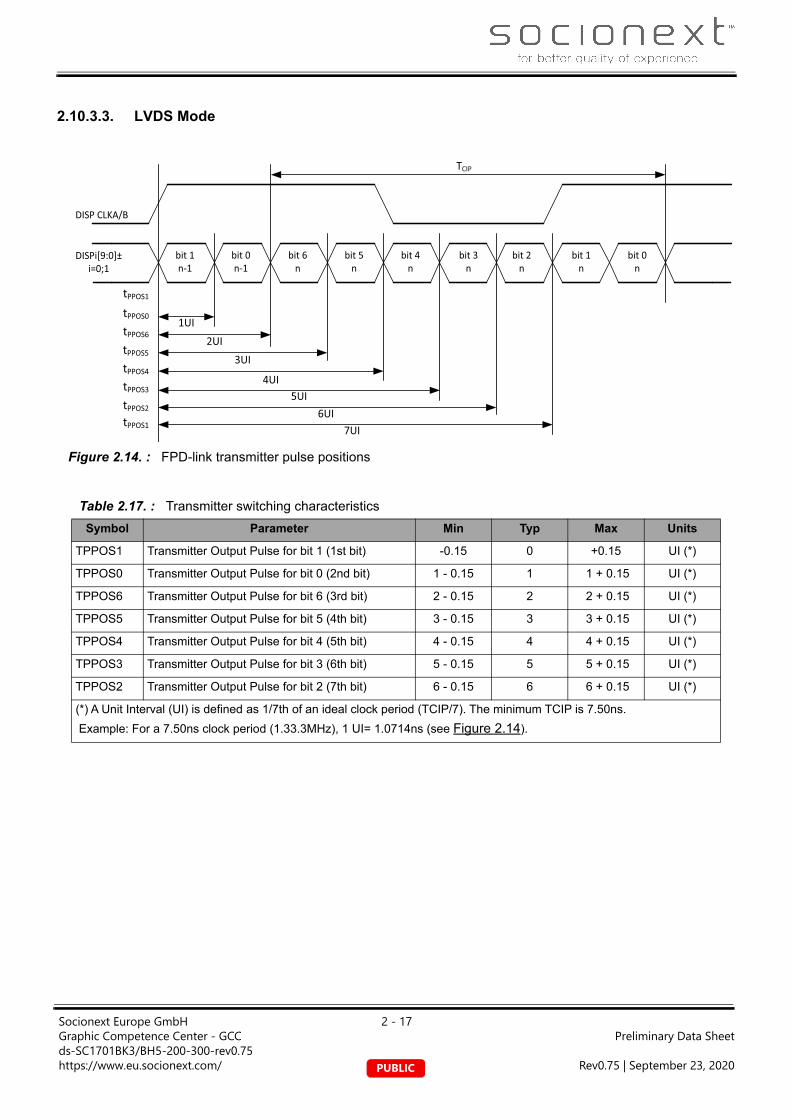
2.10.3.3. LVDS Mode
Figure 2.14. : FPD-link transmitter pulse positions
Table 2.17. : Transmitter switching characteristics
Symbol Parameter Min Typ Max Units
TPPOS1 Transmitter Output Pulse for bit 1 (1st bit) -0.15 0 +0.15 UI (*)
TPPOS0 Transmitter Output Pulse for bit 0 (2nd bit) 1 - 0.15 1 1 + 0.15 UI (*)
TPPOS6 Transmitter Output Pulse for bit 6 (3rd bit) 2 - 0.15 2 2 + 0.15 UI (*)
TPPOS5 Transmitter Output Pulse for bit 5 (4th bit) 3 - 0.15 3 3 + 0.15 UI (*)
TPPOS4 Transmitter Output Pulse for bit 4 (5th bit) 4 - 0.15 4 4 + 0.15 UI (*)
TPPOS3 Transmitter Output Pulse for bit 3 (6th bit) 5 - 0.15 5 5 + 0.15 UI (*)
TPPOS2 Transmitter Output Pulse for bit 2 (7th bit) 6 - 0.15 6 6 + 0.15 UI (*)
(*) A Unit Interval (UI) is defined as 1/7th of an ideal clock period (TCIP/7). The minimum TCIP is 7.50ns.
Example: For a 7.50ns clock period (1.33.3MHz), 1 UI= 1.0714ns (see Figure 2.14).
bit 1n-1
bit 0n-1
bit 6n
bit 5n
bit 4n
bit 3n
bit 2n
bit 1n
bit 0n
TCIP
DISP CLKA/B
DISPi[9:0]± i=0;1
tPPOS1
tPPOS0
tPPOS6
tPPOS5
tPPOS4
tPPOS3
tPPOS2
tPPOS1
1UI2UI
3UI
4UI5UI
6UI7UI
Socionext Europe GmbH 2 - 17Graphic Competence Center - GCC Preliminary Data Sheetds-SC1701BK3/BH5-200-300-rev0.75https://www.eu.socionext.com/ Rev0.75 | September 23, 2020PUBLIC

2.10.4. SPI Interface (External SPI and Flash SPI)
Figure 2.15. : Timing SPI interface
Table 2.18. : AC timings SPI interface
Parameter SymbolValue
Unit RemarksMin Typ Max
clk period tCK_SPI 25 nsPeriod depends on selected AHB clock frequency.
clk to output data tCQ_SPI -4 9.5 ns Active clock edge depends on inter-face setup.
input data setup tSU_SPI15
7.5
ns
ns
Active clock edge depends on inter-face setup.
No re-timing mode.
Re-timing mode.
input data hold tHD_SPI-3
2.5
ns
ns
Active clock edge depends on
interface setup.
No re-timing mode.
Re-timing mode.
SCLK
SDOCS
tSU_SPI tHD_SPI
tCQ_SPI(max) tCQ_SPI(min)
SDI
tCK_SPI tCK_SPI
Socionext Europe GmbH 2 - 18Graphic Competence Center - GCC Preliminary Data Sheetds-SC1701BK3/BH5-200-300-rev0.75https://www.eu.socionext.com/ Rev0.75 | September 23, 2020PUBLIC

2.10.5. I2C Interface
The SC1701BK3-200 / SC1701BH5-200/300 fulfills the timing requirements for the standard mode and fast mode of the Philips I2C specification.
The supply voltage to the I2C-bus lines (SDA and SCL) must not exceed the power-supply voltage of this I/O cell (VDE).
Voltage must not be supplied to the I2C-bus lines (SDA and SCL) if the power supply of this I/O cell (VDE) is Off.
2.10.6. USART/LIN Interface
Figure 2.16. : Timing U(S)ART interface
Table 2.19. : AC timings U(S)ART interface
Parameter SymbolValue
Unit RemarksMin Typ Max
CLK period tCK_USART 4 x trbus_clk ns
CLK to output data tCQ_USART -520
2 x trbus_clk + 45ns
Internal CLK mode
External CLK mode
Input data setup tSU_USART trbus_clk + 25 ns
Input data hold tHD_USART trbus_clk ns
USART_CLK
USART_DO
tCQ_USART(max) tCQ_USART(min)
tCK_USART
USARTn_ESCR.SCES = 1
USART_CLKUSARTn_ESCR.
SCES = 0
tHD_USARTtSU_USART
USART_DI
Socionext Europe GmbH 2 - 19Graphic Competence Center - GCC Preliminary Data Sheetds-SC1701BK3/BH5-200-300-rev0.75https://www.eu.socionext.com/ Rev0.75 | September 23, 2020PUBLIC

2.10.7. I2S Interface
Figure 2.17. : Timing I2S interface
Table 2.20. : AC timings I2S interface
Parameter SymbolValue
Unit RemarksMin Typ Max
MCLK period tMCK_I2S 18.5 ns
SCLK period tCK_I2S 37 ns Half frequency of MCLK.
MCLK to SCLK delay tDMS_I2S 0 10 ns
SCLK to output data tCQ_I2S -5 10 ns
I2S_SCLK
I2S_SDI2S_WS
tCQ_I2S(max) tCQ_I2S(min)
tCK_I2S
I2S_MCLK
tMCK_I2StDMS_I2S
I2S_SCLK
Socionext Europe GmbH 2 - 20Graphic Competence Center - GCC Preliminary Data Sheetds-SC1701BK3/BH5-200-300-rev0.75https://www.eu.socionext.com/ Rev0.75 | September 23, 2020PUBLIC

2.10.8. MII Interface
All MIII AC timings are analyzed based on the pinmux groups M7-M11 EXTMAC_MII and M19-M22 EXTPHY_MII (see attachment Pinmux_MII_RMII.xlsx in Hardware Manual). For other pinmux settings the AC timing cannot be guaranteed.
Figure 2.18. : AC Timing MII (external PHY)
Table 2.21. : AC Timing MII (external PHY)
Parameter SymbolValue
Unit CommentMin Typ Max
MII_CLK period tCK_MII
40
400ns
ns
100Mbit
10Mbit
2)
Output delay tCQ_MII 4 20 ns 1)
Input data setup tSU_MII 10 ns 2)
Input data hold tHD_MII 10 ns 2)
1) For 8mA drive strength setting, 20pF Load DISP* IOs, 30pF other IOs
2) Input transition 2.0ns
EXTPHY_MII_RXCLK(input)
EXTPHY_MII_TXD[3:0],EXTPHY_MII_TXEN
(output)
tCQ_MII(max) tCQ_MII(min)
EXTPHY_MII_TXCLK(input)
tSU_MII tHD_MII
tCK_MII
EXTPHY_MII_RXD[3:0],EXTPHY_MII_RX_DV,EXTPHY_MII_RX_ER
(input)
tCK_MII
Socionext Europe GmbH 2 - 21Graphic Competence Center - GCC Preliminary Data Sheetds-SC1701BK3/BH5-200-300-rev0.75https://www.eu.socionext.com/ Rev0.75 | September 23, 2020PUBLIC

Figure 2.19. : AC Timing MII (internal PHY, external MAC is connected)
Table 2.22. : AC Timing MII (internal PHY)
Parameter SymbolValue
Unit CommentMin Typ Max
MII_CLK period
(output)tCK_MII
40
400
ns
ns
100Mbit
10Mbit
3)
Duty cycle 40% 60% 3)
Output delay tCQ_MII 12 23 ns 1)
Input data setup tSU_MII 10 ns 2)
Input data hold tHD_MII 0 ns 2)
1) For 8mA drive strength setting, 20pF Load DISP* IOs, 30pF other IOs
2) Input Transition 2.0ns , SMT=0
3) For maximum drive strength , 20pF Load DISP* IOs, 30pF other IOs
EXTMAC_MII_RX_CLK(output)
EXTMAC_MII_TXD[3:0],EXTMAC_MII_TXEN
(input)
tCQ_MII(max) tCQ_MII(min)
EXTMAC_MII_TX_CLK(output)
tSU_MII tHD_MII
tCK_MII
EXTMAC_MII_RXD[3:0],EXTMAC_MII_RX_DV,EXTMAC_MII_RX_ER
(output)
tCK_MII
Socionext Europe GmbH 2 - 22Graphic Competence Center - GCC Preliminary Data Sheetds-SC1701BK3/BH5-200-300-rev0.75https://www.eu.socionext.com/ Rev0.75 | September 23, 2020PUBLIC

2.10.9. RMII Interface
Only RMII reference clock output is supported.
All RMIII AC timings are analyzed based on the pinmux groups M1-M5 EXTMAC_RMII and M12-M16 EXTPHY
_RMII(see attachment Pinmux_MII_RMII.xlsx in HM). For other pinmux settings the AC timing cannot be
guaranteed.
Figure 2.20. : AC Timing RMII (external PHY)
Figure 2.21. : AC Timing RMII (external MAC)
Table 2.23. : AC Timing RMII
Parameter SymbolValue
Unit CommentMin Typ Max
RMII CLK period tCK RMII 20 ns100Mbit
2)
Duty cycle 35% 65% 2)
Output delay tCQ RMII 2 11 ns 1), 4)
Input data setup tSU RMII 4 ns 3)
EXTPHY_RMII_CLK(output)
EXTPHY_RMII_TXD[1:0],EXTPHY_RMII_TXEN
(output)
tCQ_RMII(max) tCQ_RMII(min)
EXTPHY_RMII_CLK(output)
tSU_RMII tHD_RMII
tCK_RMII
EXTPHY_RMII_RXD[1:0],EXTPHY_RMII_RX_DV,EXTPHY_RMII_RX_ER
(input)
tCK_RMII
EXTMAC_RMII_CLK(output)
EXTMAC_RMII_TXD[1:0],EXTMAC_RMII_TXEN
(input)
tCQ_RMII(max) tCQ_RMII(min)
EXTMAC_RMII_CLK(output)
tSU_RMII tHD_RMII
tCK_RMIItCK_RMII
EXTPHY_RMII_RXD[1:0], EXTPHY_RMII_RX_DV,EXTPHY_RMII_RX_ER
(output)
Socionext Europe GmbH 2 - 23Graphic Competence Center - GCC Preliminary Data Sheetds-SC1701BK3/BH5-200-300-rev0.75https://www.eu.socionext.com/ Rev0.75 | September 23, 2020PUBLIC
Input data hold tHD RMII 2 ns 3)
1) For 8mA drive strength setting, 20pF Load DISP* IOs, 30pF other IO
2) For maximum drive strength, 20pF Load DISP* IOs, 30pF other IO
3) Input Transition 2.0ns, SMT=0
4) Max output delay 13ns for M1 (TSIG0* DISP0* IOs)
Table 2.23. : AC Timing RMII (Continued)
Parameter SymbolValue
Unit CommentMin Typ Max
Socionext Europe GmbH 2 - 24Graphic Competence Center - GCC Preliminary Data Sheetds-SC1701BK3/BH5-200-300-rev0.75https://www.eu.socionext.com/ Rev0.75 | September 23, 2020PUBLIC
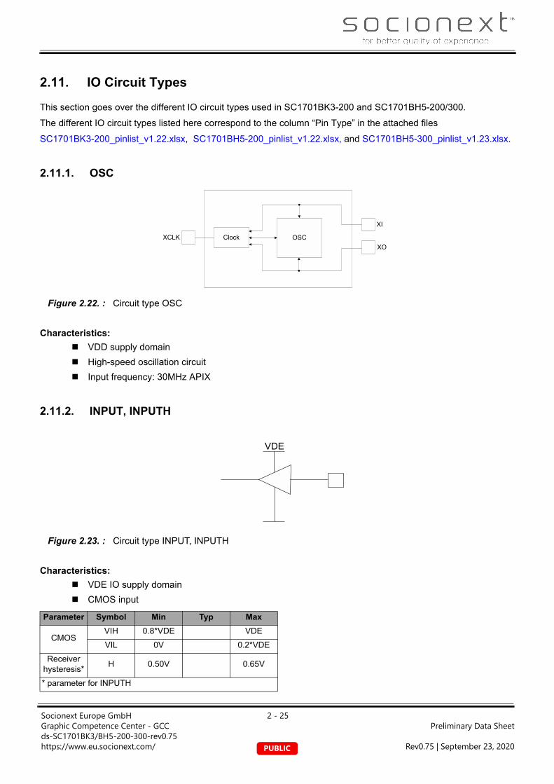
2.11. IO Circuit Types
This section goes over the different IO circuit types used in SC1701BK3-200 and SC1701BH5-200/300.
The different IO circuit types listed here correspond to the column “Pin Type” in the attached files
SC1701BK3-200_pinlist_v1.22.xlsx, SC1701BH5-200_pinlist_v1.22.xlsx, and SC1701BH5-300_pinlist_v1.23.xlsx.
2.11.1. OSC
Figure 2.22. : Circuit type OSC
Characteristics:
VDD supply domain
High-speed oscillation circuit
Input frequency: 30MHz APIX
2.11.2. INPUT, INPUTH
Figure 2.23. : Circuit type INPUT, INPUTH
Characteristics:
VDE IO supply domain
CMOS input
Parameter Symbol Min Typ Max
CMOSVIH 0.8*VDE VDE
VIL 0V 0.2*VDE
Receiver hysteresis*
H 0.50V 0.65V
* parameter for INPUTH
OSCClockXCLK
XI
XO
VDE
Socionext Europe GmbH 2 - 25Graphic Competence Center - GCC Preliminary Data Sheetds-SC1701BK3/BH5-200-300-rev0.75https://www.eu.socionext.com/ Rev0.75 | September 23, 2020PUBLIC

2.11.3. BIDI33
Figure 2.24. : Circuit type BIDI33
Characteristics:
VDE IO supply domain
CMOS level output
Programmable output drive strength
CMOS SCMITT input
Programmable pull-up and pull-down resistor
Parameter Symbol Min Typ Max
High output VOH VDE-0.5V VDE
Low output VOL 0V 0.4V
Drive Setting Symbol Min Typ Max
00 IOL / IOH 2 ± 1mA
01 IOL / IOH 4 ± 1mA
10 IOL / IOH 8 ± 1mA
11 IOL / IOH 12 ± 1mA
Parameter Symbol Min Typ Max
CMOSVIH 0.8*VDE VDE
VIL 0V 0.2*VDE
Parameter Symbol Min Typ Max
Pull-up / pull-down
R 35kOhm 60kOhm 120kOhm
Repeater
2
2
PAD
Slew Rate Control
OEN
I
Drive Strength [2:1]
Schmitt Trigger SMT
Receives Enable REN
Driver Disabled State Control P[2:1]
C
Socionext Europe GmbH 2 - 26Graphic Competence Center - GCC Preliminary Data Sheetds-SC1701BK3/BH5-200-300-rev0.75https://www.eu.socionext.com/ Rev0.75 | September 23, 2020PUBLIC
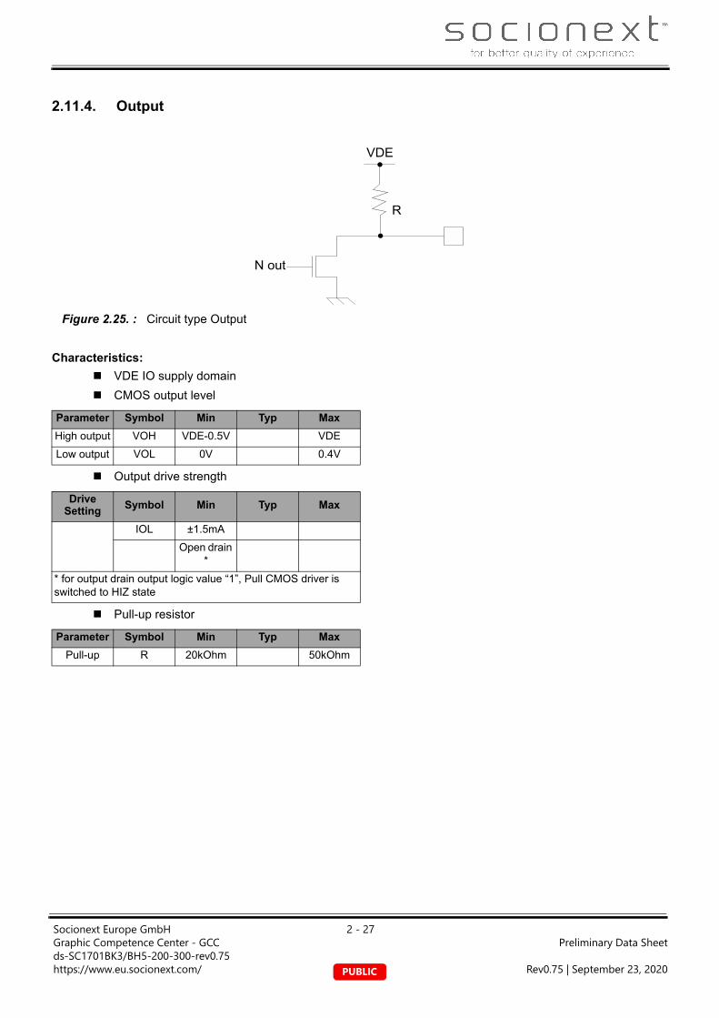
2.11.4. Output
Figure 2.25. : Circuit type Output
Characteristics:
VDE IO supply domain
CMOS output level
Output drive strength
Pull-up resistor
Parameter Symbol Min Typ Max
High output VOH VDE-0.5V VDE
Low output VOL 0V 0.4V
Drive Setting
Symbol Min Typ Max
IOL ±1.5mA
Open drain *
* for output drain output logic value “1”, Pull CMOS driver is switched to HIZ state
Parameter Symbol Min Typ Max
Pull-up R 20kOhm 50kOhm
VDE
N out
R
Socionext Europe GmbH 2 - 27Graphic Competence Center - GCC Preliminary Data Sheetds-SC1701BK3/BH5-200-300-rev0.75https://www.eu.socionext.com/ Rev0.75 | September 23, 2020PUBLIC

2.11.5. Analog
Figure 2.26. : Circuit type Analog
Characteristics:
VDDEA IO supply domain
Analog Pin
Type INPUT: Analog input pin with ESD protection
Type Output: Analog output line with ESD protection.
Analog Line
VDDEA
Socionext Europe GmbH 2 - 28Graphic Competence Center - GCC Preliminary Data Sheetds-SC1701BK3/BH5-200-300-rev0.75https://www.eu.socionext.com/ Rev0.75 | September 23, 2020PUBLIC
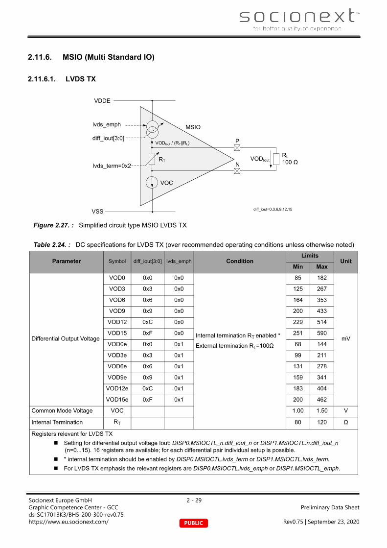
2.11.6. MSIO (Multi Standard IO)
2.11.6.1. LVDS TX
Figure 2.27. : Simplified circuit type MSIO LVDS TX
Table 2.24. : DC specifications for LVDS TX (over recommended operating conditions unless otherwise noted)
Parameter Symbol diff_iout[3:0] lvds_emph ConditionLimits
UnitMin Max
Differential Output Voltage
VOD0 0x0 0x0
Internal termination RT enabled *
External termination RL=100Ω
85 182
mV
VOD3 0x3 0x0 125 267
VOD6 0x6 0x0 164 353
VOD9 0x9 0x0 200 433
VOD12 0xC 0x0 229 514
VOD15 0xF 0x0 251 590
VOD0e 0x0 0x1 68 144
VOD3e 0x3 0x1 99 211
VOD6e 0x6 0x1 131 278
VOD9e 0x9 0x1 159 341
VOD12e 0xC 0x1 183 404
VOD15e 0xF 0x1 200 462
Common Mode Voltage VOC 1.00 1.50 V
Internal Termination RT 80 120 Ω
Registers relevant for LVDS TX
Setting for differential output voltage Iout: DISP0.MSIOCTL_n.diff_iout_n or DISP1.MSIOCTL.n.diff_iout_n (n=0...15). 16 registers are available; for each differential pair individual setup is possible.
* internal termination should be enabled by DISP0.MSIOCTL.lvds_term or DISP1.MSIOCTL.lvds_term.
For LVDS TX emphasis the relevant registers are DISP0.MSIOCTL.lvds_emph or DISP1.MSIOCTL_emph.
VOC
VDDE
VSS
P
NVODIout
diff_iout=0,3,6,9,12,15
RTRL
100 Ω
VODIout / (RT||RL)
MSIO
diff_iout[3:0]
lvds_term=0x2
lvds_emph
Socionext Europe GmbH 2 - 29Graphic Competence Center - GCC Preliminary Data Sheetds-SC1701BK3/BH5-200-300-rev0.75https://www.eu.socionext.com/ Rev0.75 | September 23, 2020PUBLIC

The diagrams in Figure 2.28 show the emphasis impact on the LVDS signal wave form.
Figure 2.28. : LVDS signal wave form
The LVDS IO cell (MSIO) includes a driver that generates the nominal differential swing VOD. An additional delayed driver could drop swing level VOD to the level VODe in case the lvds_emph bit is set.
This function can improve the signal integrity, e.g., if longer cables are used.
Note: For higher LVDS bandwidth (>600Mbps/lane) the EHS (Enable High Speed) should be enabled.
Table 2.25. : AC Specifications (over recommended operating conditions unless otherwise noted)
Parameter Symbol ConditionLimits
UnitMin Typ Max
LVDS Channel to Channel Skew ChSkew 100 ps
Cycle to N-Cycle Jitter, N=7 Jcc 100 mUI
Pre-Emphasis Time Temph 1 ns
VODlvds_emph=0
VOD VODe
Temph
lvds_emph=0
Socionext Europe GmbH 2 - 30Graphic Competence Center - GCC Preliminary Data Sheetds-SC1701BK3/BH5-200-300-rev0.75https://www.eu.socionext.com/ Rev0.75 | September 23, 2020PUBLIC

2.11.6.2. LVDS RX
Figure 2.29. : Simplified circuit type MSIO LVDS RX
Table 2.26. : DC specifications (over recommended operating conditions unless otherwise noted)
Parameter Symbol ConditionLimits
Unit CommentMin Max
Differential Input Swing VOC
Internal termination RT
enabled
160 600 mV VIH and VIL must not be violatedInput Common Mode VIC 0.5 1.7 V
Single-ended input high voltage VIH 1.78 V
Single-ended input low voltage VIL 0.42 V
Internal Termination RT 80 120 Ω*lvds_term must be set to 0x02
Registers relevant for LVDS RX
For LVDS Iout the relevant registers are CAP0.MSIOCTL_n.diff_iout_n or CAP1.MSIOCTL_n.diff_iout_n (n=0...5). 6 registers are available; for each differential pair individual setup is possible.
The recommended value for LVDS capture is 0x9.
P
NRT
*lvds_term=0x2
MSIO
Socionext Europe GmbH 2 - 31Graphic Competence Center - GCC Preliminary Data Sheetds-SC1701BK3/BH5-200-300-rev0.75https://www.eu.socionext.com/ Rev0.75 | September 23, 2020PUBLIC

2.11.6.3. miniLVDS TX
Figure 2.30. : Circuit type MSIO miniLVDS Tx
The diagrams in Figure 2.31 show the emphasis impact on the LVDS signal wave form.
Table 2.27. : DC specifications for miniLVDS (over recommended operating conditions unless otherwise noted)
Parameter Symbol diff_iout[3:0] lvds_emph ConditionLimits
UnitMin Max
Differential Output Voltage
VOD9 0x9 0x0
Internal termination RT enabled*
External termination RL=100Ω
200 433
mV
VOD12 0xC 0x0 229 514
VOD15 0xF 0x0 251 590
VOD9e 0x9 0x1 159 341
VOD12e 0xC 0x1 183 404
VOD15e 0xF 0x1 200 462
Common Mode Voltage VOC 1.00 1.50 V
Internal Termination RT 80 120 Ω
Registers relevant for LVDS TX
Setting for differential output voltage Iout: DISP0.MSIOCTL_n.diff_iout_n or DISP1.MSIOCTL.n.diff_iout_n (n=0...15). 16 registers are available, for each differential pair individual setup is possible.
* internal termination should be enabled by DISP0.MSIOCTL.lvds_term or DISP1.MSIOCTL.lvds_term.
For LVDS TX emphasis the relevant registers are DISP0.MSIOCTL.lvds_emph or DISP1.MSIOCTL.lvds_emph.
VOC
VDDE
VSS
P
NVODIout
diff_iout=0,3,6,9,12,15
RTRL
100 Ω
VODIout / (RT||RL)
MSIO
diff_iout[3:0]
lvds_term*=0x2
lvds_emph
Socionext Europe GmbH 2 - 32Graphic Competence Center - GCC Preliminary Data Sheetds-SC1701BK3/BH5-200-300-rev0.75https://www.eu.socionext.com/ Rev0.75 | September 23, 2020PUBLIC

Figure 2.31. : LVDS signal wave form
The LVDS IO cell (MSIO) includes a driver that generates the nominal differential swing VOD. An additional delayed driver could drop swing level VOD to the level VODe in case the lvds_emph bit is set.
This function can improve the signal integrity, e.g., if longer cables are used.
Note: For higher LVDS bandwidth (>600Mbps/lane) the EHS (Enable High Speed) should be enabled.
Table 2.28. : AC Specifications (over recommended operating conditions unless otherwise noted)
Parameter Symbol ConditionLimits
UnitMin Typ Max
LVDS Channel to Channel Skew ChSkew 100 ps
Cycle to N-Cycle Jitter, N=7 Jcc 100 mUI
Pre-Emphasis Time Temph 1 ns
VODlvds_emph=0
VOD VODe
Temph
lvds_emph=0
Socionext Europe GmbH 2 - 33Graphic Competence Center - GCC Preliminary Data Sheetds-SC1701BK3/BH5-200-300-rev0.75https://www.eu.socionext.com/ Rev0.75 | September 23, 2020PUBLIC

2.11.6.4. RSDS TX SST (Single Sided Termination)
Figure 2.32. : Circuit type MSIO RSDS TX SST
Figure 2.33. : RSDS signal wave form
Table 2.29. : DC specifications (over recommended operating conditions unless otherwise noted)
Parameter Symbol diff_iout[3:0] lvds_emph ConditionLimits
UnitMin Max
Differential Output VoltageVOD0 0x0 0x0
Internal termination RT disabled
(high impedance) *
External termination RL=100Ω
167 330mV
VOD3 0x3 0x0 245 485
Common Mode Voltage VOC 1.00 1.50 V
Internal Termination RT high impedance Ω
Relevant registers for RSDS TX (SST)
Setting for differential output voltage Iout: DISP0.MSIOCTL_n.diff_iout_n or DISP1.MSIOCTL_n.diff_iout_n (n=0...15). 16 registers are available; for each differential pair individual setup is possible.
* the internal termination should be enabled by DISP0.MSIOCTL.lvds_term or DISP1.MSIOCTL.lvds_term.
For LVDS TX emphasis the relevant registers are DISP0.MSIOCTL.lvds_emph or DISP1.MSIOCTL.lvds_emph.
Table 2.30. : AC Specifications (over recommended operating conditions unless otherwise noted)
Parameter Symbol ConditionLimits
UnitMin Typ Max
LVDS Channel to Channel Skew ChSkew 100 ps
Cycle to N-Cycle Jitter, N=7 Jcc 100 mUI
VOC
VDDE
VSS
P
NVODIout
diff_iout=3,6,9,12,15
RTRL
100 Ω
VODIout / (RT||RL)
MSIO
diff_iout[3:0]
lvds_term*=0x0(high impedance)
VODlvds_emph=0
Socionext Europe GmbH 2 - 34Graphic Competence Center - GCC Preliminary Data Sheetds-SC1701BK3/BH5-200-300-rev0.75https://www.eu.socionext.com/ Rev0.75 | September 23, 2020PUBLIC
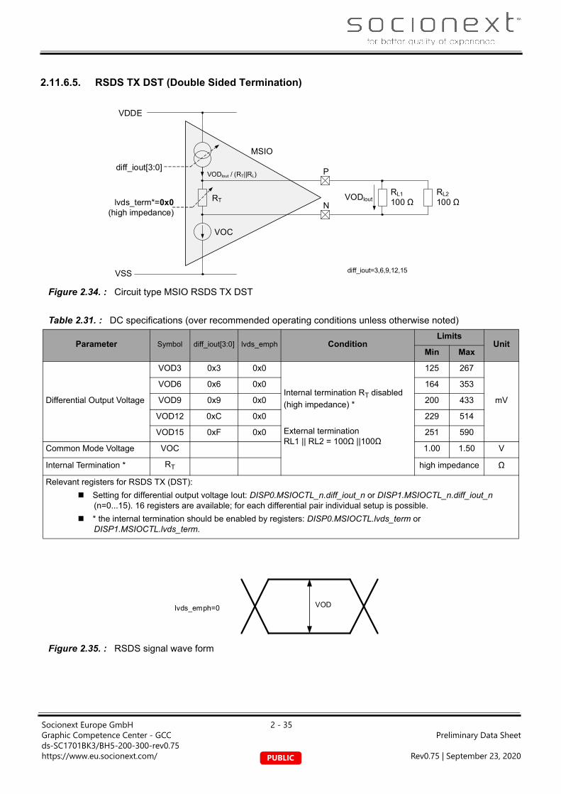
2.11.6.5. RSDS TX DST (Double Sided Termination)
Figure 2.34. : Circuit type MSIO RSDS TX DST
Figure 2.35. : RSDS signal wave form
Table 2.31. : DC specifications (over recommended operating conditions unless otherwise noted)
Parameter Symbol diff_iout[3:0] lvds_emph ConditionLimits
UnitMin Max
Differential Output Voltage
VOD3 0x3 0x0
Internal termination RT disabled
(high impedance) *
External termination RL1 || RL2 = 100Ω ||100Ω
125 267
mV
VOD6 0x6 0x0 164 353
VOD9 0x9 0x0 200 433
VOD12 0xC 0x0 229 514
VOD15 0xF 0x0 251 590
Common Mode Voltage VOC 1.00 1.50 V
Internal Termination * RT high impedance Ω
Relevant registers for RSDS TX (DST):
Setting for differential output voltage Iout: DISP0.MSIOCTL_n.diff_iout_n or DISP1.MSIOCTL_n.diff_iout_n (n=0...15). 16 registers are available; for each differential pair individual setup is possible.
* the internal termination should be enabled by registers: DISP0.MSIOCTL.lvds_term or DISP1.MSIOCTL.lvds_term.
VOC
VDDE
VSS
P
NVODIout
diff_iout=3,6,9,12,15
RTRL1
100 Ω
VODIout / (RT||RL)
MSIO
diff_iout[3:0]
lvds_term*=0x0(high impedance)
RL2
100 Ω
VODlvds_emph=0
Socionext Europe GmbH 2 - 35Graphic Competence Center - GCC Preliminary Data Sheetds-SC1701BK3/BH5-200-300-rev0.75https://www.eu.socionext.com/ Rev0.75 | September 23, 2020PUBLIC

Table 2.32. : AC Specifications (over recommended operating conditions unless otherwise noted)
Parameter Symbol ConditionLimits
UnitMin Typ Max
LVDS Channel to Channel Skew ChSkew 100 ps
Cycle to N-Cycle Jitter, N=7 Jcc 100 mUI
Socionext Europe GmbH 2 - 36Graphic Competence Center - GCC Preliminary Data Sheetds-SC1701BK3/BH5-200-300-rev0.75https://www.eu.socionext.com/ Rev0.75 | September 23, 2020PUBLIC

2.11.6.6. TTL
Figure 2.36. : Circuit type TTL
One MSIO cell includes two BIDE33 cells and the PADs are connected to the pins EBP_X and EBN_X (X:0,1). The “Receiver Enable REN” and the “Output Enable OEN” are controlled by the related multiplex function. The remaining ports are controlled by the registers in Table 2.33 .
Table 2.33. : TTL-relevant registers
MSIO TTL Control Ports MSIO Control Registers
Slew Rate ControlMSIOCTL_X.ttl_srcn_X
MSIOCTL_X.ttl_srcp_X
(X:0,1)
Drive Strength [2:1]MSIOCTL_X.csn_X
MSIOCTL_X.csp_X
(X:0,1)
Schmitt TriggerMSIOCTL_X.smtn_X
MSIOCTL_X.smtp_X
(X:0,1)
Drive Disabled State Control P[2:1]MSIOCTL_X.ttl_dsn_X
MSIOCTL_X.ttl_dsp_X
(X:0,1)
Repeater
2
2
PAD
Slew Rate Control
OEN
I
Drive Strength [2:1]
Schmitt Trigger SMT
Receives Enable REN
Driver Disabled State Control P[2:1]
C
Socionext Europe GmbH 2 - 37Graphic Competence Center - GCC Preliminary Data Sheetds-SC1701BK3/BH5-200-300-rev0.75https://www.eu.socionext.com/ Rev0.75 | September 23, 2020PUBLIC

Characteristics
VDE IO supply domain
CMOS output level
Programmable output drive strength
CMOS SCHMITT input
Programmable pull-up/pull-down resistor
Parameter Symbol Min Typ Max
High output VOH VDE-0.5V VDE
Low output VOL 0V 0.5V
Drive Setting Symbol Min Typ Max
00 IOL / IOH 2 ± 1mA
01 IOL / IOH 4 ± 1mA
10 IOL / IOH 8 ± 1mA
11 IOL / IOH 12 ± 12mA
Parameter Symbol Min Typ Max
CMOSVIH 0.8*VDE VDE
VIL 0V 0.2*VDE
Parameter Symbol Min Typ Max
Pull-up/pull-down
R 35kOhm 60kOhm 120kOhm
Socionext Europe GmbH 2 - 38Graphic Competence Center - GCC Preliminary Data Sheetds-SC1701BK3/BH5-200-300-rev0.75https://www.eu.socionext.com/ Rev0.75 | September 23, 2020PUBLIC

Socionext Europe GmbHGraphic Competence Center - GCC Preliminary Data Sheetds-SC1701BK3/BH5-200-300-rev0.75 Warranty and Disclaimerhttps://www.eu.socionext.com/ Rev0.75 | September 23, 2020PUBLIC
Warranty and Disclaimer
The contents of this document are subject to change without notice. Customers are advised to consult with sales representatives before ordering.
The information, such as descriptions of function and application circuit examples, in this document are presented solely for the purpose of reference to show examples of operations and uses of SOCIONEXT EUROPE GMBH devices.
SOCIONEXT EUROPE GMBH does not warrant proper operation of the device with respect to use based on such information. When you develop equipment incorporating the device based on such information, you must assume any responsibility arising out of such use of the information. SOCIONEXT EUROPE GMBH assumes no liability for any damages whatsoever arising out of the use of the information.
Any information in this document, including descriptions of function and schematic diagrams, shall not be construed as license of the use or exercise of any intellectual property right, such as patent right or copyright, or any other right of SOCIONEXT EUROPE GMBH or any third party nor does SOCIONEXT EUROPE GMBH warrant non-infringement of any third-party's intellectual property right or other right by using such information. SOCIONEXT EUROPE GMBH assumes no liability for any infringement of the intellectual property rights or other rights of third parties which would result from the use of information contained herein.
The products described in this document are designed, developed and manufactured as contemplated for general use, including without limitation, ordinary industrial use, general office use, personal use, and household use, but are not designed, developed and manufactured as contemplated (1) for use accompanying fatal risks or dangers that, unless extremely high safety is secured, could have a serious effect to the public, and could lead directly to death, personal injury, severe physical damage or other loss (i.e., nuclear reaction control in nuclear facility, aircraft flight control, air traffic control, mass transport control, medical life support system, missile launch control in weapon system), or (2) for use requiring extremely high reliability (i.e., submersible repeater and artificial satellite).
Please note that SOCIONEXT EUROPE GMBH will not be liable against you and/or any third party for any claims or damages arising in connection with above-mentioned uses of the products.
Any semiconductor device has an inherent chance of failure. You must protect against injury, damage or loss from such failures by incorporating safety design measures into your facility and equipment such as redundancy, fire protection, and prevention of over-current levels and other abnormal operating conditions.
Exportation/release of any products described in this document may require necessary procedures in accordance with the regulations of the Foreign Exchange and Foreign Trade Control Law of Japan and/or US export control laws.
The company names and brand names herein are the trademarks or registered trademarks of their respective owners.