preliminary technical data a
TRANSCRIPT

aPreliminary Technical Data
This information applies to a product under development. Its characteristicsand specifications are subject to change without notice. Analog Devices assumes no obligation regarding future manufacturing unless otherwiseagreed to in writing.
One Technology Way, P.O.Box 9106, Norwood, MA 02062-9106, U.S.A.Tel:781/329-4700 World Wide Web Site: http://www.analog.comFax:781/326-8703 ©Analog Devices,Inc., 2001
REV. PrA
PRELIMINARY TECHNICAL DATA
ADSP-21532FEATURES
300 MHz High-Performance MSA DSP Core
Two 16-Bit MACs, Two 40-Bit ALUs, Four 8-Bit Video
ALUs, 40-Bit Shifter
RISC-Like Register and Instruction Model for Ease of
Programming and Compiler-Friendly Support
Advanced Debug, Trace, and Performance- Monitoring
Support
On-chip Voltage Regulation from 2.25 V to 3.6 V Input
3.3 V-Tolerant I/O
-25 ºC to 105 ºC Case Temperature Range
160-Lead Mini-BGA Package
MEMORY
116K Bytes of On-Chip Memory:
16K Bytes of Instruction SRAM/Cache
32K Bytes of Instruction SRAM
32K Bytes of Instruction ROM
32K Bytes of Data SRAM/Cache
4K Bytes of Scratchpad SRAM
Memory DMA Controller
Memory Management Unit Providing Memory
Protection
Synchronous External Memory Controller with Glueless
SDRAM Support
Asynchronous External Memory Controller with
Glueless Support for SRAM, FLASH, ROM
Flexible Memory Booting Options From SPI, External
Memory, or Internal ROM
PERIPHERALS
Parallel Peripheral Interface (PPI) Port/GPIO, Supporting
CCIR-656 Video Data Formats
Two Dual-Channel, Full-Duplex Synchronous Serial
Ports, Supporting Eight Stereo I2S Channels
SPI-compatible Port
Three Timer/Counters with PWM Support
UART with Support for IrDA®
Event Handler
Real-Time Clock
Watchdog Timer
Debug/JTAG Interface
On Chip PLL Capable of 1x To 31x Frequency
Multiplication
ADSP-21532 BLACKFIN DSP BLOCK DIAGRAM
SYSTEM BUSINTERFACE UNIT
DMACONTROLLER
84K BYTES SRAM
32K BYTES ROM
EVENTCONTROLLER/CORE TIMER
REAL TIME CLOCK
UART PORTIrDA®
TIMER0, TIMER1,TIMER2
PPI PORT
SERIAL PORTS (2)
SPI PORT
EXTERNAL PORTFLASH, SDRAMCONTROL
BOOT ROM
JTAG TEST ANDEMULATION WATCHDOG TIMER
VOLTAGEREGULATOR
MICROSIGNAL
ARCHITECTURECORE

For current information contact Analog Devices at 800-262-5643ADSP-21532 September 2001
This information applies to a product under development. Its characteristics and specifications are subject to change with-out notice. Analog Devices assumes no obligation regarding future manufacturing unless otherwise agreed to in writing.
2 REV. PrA
PRELIMINARY TECHNICAL DATA
General NoteThis data sheet provides preliminary information for the ADSP-21532 BlackfinTM DSP1.
GENERAL DESCRIPTIONThe ADSP-21532 is a member of the Blackfin DSP family of products, incorporating the Analog Devices/Intel Micro Signal Architecture (MSA). Blackfin DSPs combine a dual-MAC state-of-the-art DSP engine, the advantages of a clean, orthogonal RISC-like microprocessor instruction set, and single-instruction, multiple-data (SIMD) multimedia capabilities into a single instruction-set architecture.
By integrating a rich set of industry-leading system periph-erals and memory, Blackfin DSPs are the platform of choice for next-generation applications that require RISC-like pro-grammability, multimedia support and leading-edge signal processing in one integrated DSP.
Portable Low-Power ArchitectureBlackfin DSPs provide world-class power management and performance compared to other Digital Signal Processors. Blackfin DSPs are designed in a Low-Power and Low-Voltage Design Methodology and feature Dynamic Power Management, the ability to vary both the voltage and frequency of operation to significantly lower overall power consumption. Varying the voltage and frequency can result in a three-fold reduction in power consumption, by com-parison to just varying the frequency of operation. This translates into longer battery life for portable appliances.
System IntegrationThe ADSP-21532 is a highly integrated system-on-a-chip solution for the next generation of digital communication and portable Internet appliances. By combining industry-standard interfaces with a high performance Digital Signal Processing core, users can develop cost-effective solutions quickly without the need for costly external components. The ADSP-21532 system peripherals include a UART port, an SPI port, two Serial ports (SPORTs), four general purpose Timers (three with PWM capability), a Real-Time Clock, a Watchdog Timer, and a Parallel Peripheral Interface port.
ADSP-21532 PeripheralsThe ADSP-21532 contains a rich set of peripherals connected to the core via several high bandwidth buses, providing flexibility in system configuration as well as excellent overall system performance. See the block diagram on page 1. The general-purpose peripherals include functions such as UART, Timers with PWM (Pulse Width Modulation) and pulse measurement capability, general purpose flag I/O pins, a Real-Time Clock, and a Watchdog Timer. This set of functions satisfies a wide variety of typical system support needs and is augmented by the system expansion capabilities of the part. In addition to these
general-purpose peripherals, the ADSP-21532 contains high speed serial and parallel ports for interfacing to a variety of audio, video, and modem CODEC functions; an interrupt controller for flexible management of interrupts from the on-chip peripherals or external sources; and power management control functions to tailor the performance and power characteristics of the processor and system to many application scenarios.
All of the peripherals, except for general-purpose I/O, Real-Time Clock, and timers, are supported by a flexible DMA structure. There is also a separate memory DMA channel dedicated to data transfers between the DSP's various memory spaces, including external SDRAM and asynchro-nous memory. Multiple on-chip buses running at up to 133 MHz provide adequate bandwidth to keep the processor core running along with activity on all of the on-chip and external peripherals.
The ADSP-21532 includes an on-chip voltage regulator in support of the Blackfin core Dynamic Power Management capability. The voltage regulator provides a range of core voltage levels from a single 2.25 V to 3.6 V input. The voltage regulator can be bypassed at the user's discretion.
MSA DSP CoreAs shown in Figure 1 on page 3, the MSA DSP core contains two multiplier/accumulators, two 40 bit ALU’s, four video ALU’s, and a 40 bit shifter. The computation units process 8-bit, 16-bit, or 32-bit data from the register file.
The compute register file contains eight 32-bit registers. When performing compute operations on 16-bit operand data, the register file operates as 16 independent 16-bit reg-isters. All operands for compute operations come from the multiported register file and instruction constant fields.
Each MAC can perform a 16-bit by 16-bit multiply in each cycle, accumulating the results into the 40-bit accumula-tors. Signed and unsigned formats, rounding, and saturation are supported.
The ALU’s perform a traditional set of arithmetic and logical operations on 16-bit or 32-bit data. In addition, many special instructions are included to accelerate various signal processing tasks. These include bit operations such as field extract and population count, modulo 232 multiply, divide primitives, saturation and rounding, and sign/expo-nent detection. The set of video instructions include byte alignment and packing operations, 16-bit and 8-bit adds with clipping, 8-bit average operations, and 8-bit sub-tract/absolute value/accumulate (SAA) operations. Also provided are the compare/select and vector search instructions.
For certain instructions, two 16-bit ALU operations can be performed simultaneously on register pairs (a 16-bit high half and 16-bit low half of a compute register). By also using the second ALU, quad 16-bit operations are possible.1Blackfin DSP is a trademark of Analog Devices, Inc.

This information applies to a product under development. Its characteristics and specifications are subject to change with-out notice. Analog Devices assumes no obligation regarding future manufacturing unless otherwise agreed to in writing.
3REV. PrA
For current information contact Analog Devices at 800-262-5643 ADSP-21532September 2001
PRELIMINARY TECHNICAL DATA
The 40-bit shifter can perform shifts and rotates and is used to support normalization, field extract, and field deposit instructions.
The program sequencer controls the flow of instruction exe-cution, including instruction alignment and decoding. For program flow control, the sequencer supports PC relative and indirect conditional jumps (with static branch predic-tion), and subroutine calls. Hardware is provided to support
zero-overhead looping. The architecture is fully interlocked, meaning that there are no visible pipeline effects when executing instructions with data dependencies.
The address arithmetic unit provides two addresses for simultaneous dual fetches from memory. The unit contains a multiported register file consisting of four sets of 32-bit Index, Modify, Length, and Base registers (for circular buff-ering), and eight additional 32-bit pointer registers (for C-style indexed stack manipulation).
Blackfin DSPs support a modified Harvard architecture in combination with a hierarchical memory structure. Level 1 (L1) memories are those that typically operate at the full processor speed with little or no latency. At the L1 level, the instruction memory holds instructions only. The two data memories hold data, and a dedicated scratchpad data memory stores stack and local variable information.
In addition, multiple L1 memory blocks are provided, offering a configurable mix of SRAM and cache. The Memory Management Unit (MMU) provides memory pro-tection for individual tasks that may be operating on the core and can protect system registers from unintended access.
The architecture provides three modes of operation: user mode, supervisor mode, and emulation mode. User mode has restricted access to certain system resources, thus
providing a protected software environment, while supervi-sor mode has unrestricted access to the system and core resources.
The Blackfin DSP instruction set has been optimized so that 16-bit opcodes represent the most frequently used instruc-tions, resulting in excellent compiled code density. Complex DSP instructions are encoded into 32-bit opcodes, repre-senting fully featured multifunction instructions. Blackfin DSPs support a limited multi-issue capability, where a 32-bit instruction can be issued in parallel with two 16-bit instructions, allowing the programmer to use many of the core resources in a single instruction cycle.
The Blackfin DSP assembly language uses an algebraic syntax for ease of coding and readability. The architecture has been optimized for use in conjunction with the C-compiler, resulting in fast and efficient software implementations.
Figure 1. MSA DSP Core
SP
SEQUENCER
ALIGN
DECODE
LOOP BUFFER
DAG0 DAG1
16 1 688 8 8
40 40
A0 A1
BARRELSHIFTER
DATA AR ITHMETIC UN IT
CONTROLUN IT
ADDRESS ARITHMETIC UNIT
FPP5P4P3P2P1P0
R7R6R5R4R3R2R1R0
I3I2I1I0
L3L2L1L0
B3B2B1B0
M3M2M1M0
For current information contact Analog Devices at 800-262-5643ADSP-21532 September 2001
This information applies to a product under development. Its characteristics and specifications are subject to change with-out notice. Analog Devices assumes no obligation regarding future manufacturing unless otherwise agreed to in writing.
4 REV. PrA
PRELIMINARY TECHNICAL DATA
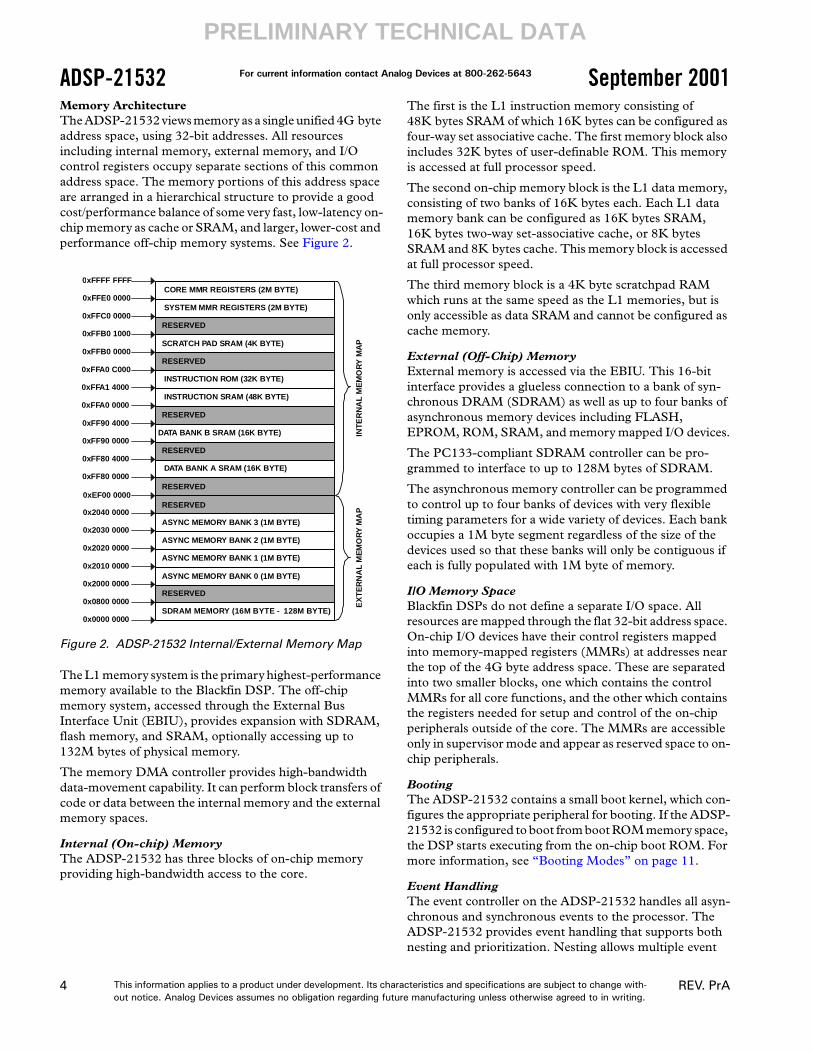
Memory ArchitectureThe ADSP-21532 views memory as a single unified 4G byte address space, using 32-bit addresses. All resources including internal memory, external memory, and I/O control registers occupy separate sections of this common address space. The memory portions of this address space are arranged in a hierarchical structure to provide a good cost/performance balance of some very fast, low-latency on-chip memory as cache or SRAM, and larger, lower-cost and performance off-chip memory systems. See Figure 2.
The L1 memory system is the primary highest-performance memory available to the Blackfin DSP. The off-chip memory system, accessed through the External Bus Interface Unit (EBIU), provides expansion with SDRAM, flash memory, and SRAM, optionally accessing up to 132M bytes of physical memory.
The memory DMA controller provides high-bandwidth data-movement capability. It can perform block transfers of code or data between the internal memory and the external memory spaces.
Internal (On-chip) MemoryThe ADSP-21532 has three blocks of on-chip memory providing high-bandwidth access to the core.
The first is the L1 instruction memory consisting of 48K bytes SRAM of which 16K bytes can be configured as four-way set associative cache. The first memory block also includes 32K bytes of user-definable ROM. This memory is accessed at full processor speed.
The second on-chip memory block is the L1 data memory, consisting of two banks of 16K bytes each. Each L1 data memory bank can be configured as 16K bytes SRAM, 16K bytes two-way set-associative cache, or 8K bytes SRAM and 8K bytes cache. This memory block is accessed at full processor speed.
The third memory block is a 4K byte scratchpad RAM which runs at the same speed as the L1 memories, but is only accessible as data SRAM and cannot be configured as cache memory.
External (Off-Chip) MemoryExternal memory is accessed via the EBIU. This 16-bit interface provides a glueless connection to a bank of syn-chronous DRAM (SDRAM) as well as up to four banks of asynchronous memory devices including FLASH, EPROM, ROM, SRAM, and memory mapped I/O devices.
The PC133-compliant SDRAM controller can be pro-grammed to interface to up to 128M bytes of SDRAM.
The asynchronous memory controller can be programmed to control up to four banks of devices with very flexible timing parameters for a wide variety of devices. Each bank occupies a 1M byte segment regardless of the size of the devices used so that these banks will only be contiguous if each is fully populated with 1M byte of memory.
I/O Memory SpaceBlackfin DSPs do not define a separate I/O space. All resources are mapped through the flat 32-bit address space. On-chip I/O devices have their control registers mapped into memory-mapped registers (MMRs) at addresses near the top of the 4G byte address space. These are separated into two smaller blocks, one which contains the control MMRs for all core functions, and the other which contains the registers needed for setup and control of the on-chip peripherals outside of the core. The MMRs are accessible only in supervisor mode and appear as reserved space to on-chip peripherals.
BootingThe ADSP-21532 contains a small boot kernel, which con-figures the appropriate peripheral for booting. If the ADSP-21532 is configured to boot from boot ROM memory space, the DSP starts executing from the on-chip boot ROM. For more information, see “Booting Modes” on page 11.
Event HandlingThe event controller on the ADSP-21532 handles all asyn-chronous and synchronous events to the processor. The ADSP-21532 provides event handling that supports both nesting and prioritization. Nesting allows multiple event
Figure 2. ADSP-21532 Internal/External Memory Map
CORE MMR REGISTERS (2M BYTE)
RESERVED
SCRATCH PAD SRAM (4K BYTE)
INSTRUCTION SRAM (48K BYTE)
SYSTEM MMR REGISTERS (2M BYTE)
RESERVED
RESERVED
DATA BANK B SRAM (16K BYTE)
RESERVED
DATA BANK A SRAM (16K BYTE)
ASYNC MEMORY BANK 3 (1M BYTE)
ASYNC MEMORY BANK 2 (1M BYTE)
ASYNC MEMORY BANK 1 (1M BYTE)
ASYNC MEMORY BANK 0 (1M BYTE)
SDRAM MEMORY (16M BYTE - 128M BYTE)
INSTRUCTION ROM (32K BYTE)
INT
ER
NA
LM
EM
OR
YM
AP
EX
TE
RN
AL
ME
MO
RY
MA
P
0xFFFF FFFF
0xFFE0 0000
0xFFB0 0000
0xFFA0 C000
0xFFA1 4000
0xFF90 4000
0xFF90 0000
0xFF80 4000
0xFF80 0000
0xEF00 0000
0x2040 0000
0x2030 0000
0x2020 0000
0x2010 0000
0x2000 0000
0x0800 0000
0x0000 0000
0xFFC0 0000
0xFFB0 1000
0xFFA0 0000
RESERVED
RESERVED
RESERVED

This information applies to a product under development. Its characteristics and specifications are subject to change with-out notice. Analog Devices assumes no obligation regarding future manufacturing unless otherwise agreed to in writing.
5REV. PrA
For current information contact Analog Devices at 800-262-5643 ADSP-21532September 2001
PRELIMINARY TECHNICAL DATA
service routines to be active simultaneously. Prioritization ensures that servicing of a higher-priority event takes pre-cedence over servicing of a lower-priority event. The controller provides support for five different types of events:
• Emulation – An emulation event causes the processor to enter emulation mode, allowing command and control of the processor via the JTAG interface.
• Reset – This event resets the processor.
• Non-Maskable Interrupt (NMI) – The NMI event can be generated by the software watchdog timer or by the NMI input signal to the processor. The NMI event is frequently used as a power-down indicator to initiate an orderly shutdown of the system.
• Exceptions – Exceptions are events that occur synchro-nously to program flow (i.e., the exception will be taken before the instruction is allowed to complete). Conditions such as data alignment violations and undefined instruc-tions cause exceptions.
• Interrupts – Interrupts are events that occur asynchro-nously to program flow. They are caused by input pins, timers, and other peripherals.
Each event type has an associated register to hold the return address and an associated return-from-event instruction. When an event is triggered, the state of the processor is saved on the supervisor stack.
The ADSP-21532 Event Controller consists of two stages, the Core Event Controller (CEC) and the System Interrupt Controller (SIC). The Core Event Controller works with the System Interrupt Controller to prioritize and control all system events. Conceptually, interrupts from the peripher-als enter into the SIC, and are then routed directly into the general-purpose interrupts of the CEC.
Core Event Controller (CEC)The CEC supports nine general-purpose interrupts (IVG15–7), in addition to the dedicated interrupt and exception events. Of these general-purpose interrupts, the two lowest-priority interrupts (IVG15–14) are recom-mended to be reserved for software interrupt handlers, leaving seven prioritized interrupt inputs to support the peripherals of the ADSP-21532. Table 1 describes the inputs to the CEC, identifies their names in the Event Vector Table (EVT), and lists their priorities.
System Interrupt Controller (SIC)The System Interrupt Controller provides the mapping and routing of events from the many peripheral interrupt sources to the prioritized general-purpose interrupt inputs of the CEC. Although the ADSP-21532 provides a default mapping, the user can alter the mappings and priorities of interrupt events by writing the appropriate values into the Interrupt Assignment Registers (IAR). Table 2 describes the inputs into the SIC and the default mappings into the CEC.
Table 1. Core Event Controller (CEC)
Priority(0 is Highest)
Event Class EVT Entry
0 Emulation/Test Control
EMU
1 Reset RST2 Non-Maskable
InterruptNMI
3 Exceptions EVX4 Global Interrupt
Enable-
5 Hardware Error IVHW6 Core Timer IVTMR7 General Interrupt 7 IVG78 General Interrupt 8 IVG89 General Interrupt 9 IVG910 General Interrupt 10 IVG1011 General Interrupt 11 IVG1112 General Interrupt 12 IVG1213 General Interrupt 13 IVG1314 General Interrupt 14 IVG1415 General Interrupt 15 IVG15
Table 2. System Interrupt Controller (SIC)
Peripheral Interrupt EventDefault Mapping
Real-Time Clock Interrupt IVG7Parallel Peripheral Interface Interrupt IVG7Rx SPORT 0 DMA Interrupt IVG8Tx SPORT 0 DMA Interrupt IVG8Rx SPORT 1 DMA Interrupt IVG8Tx SPORT 1 DMA Interrupt IVG8SPI DMA Interrupt IVG9Rx UART Interrupt IVG10Tx UART Interrupt IVG10Timer Interrupt 0 IVG11Timer Interrupt 1 IVG11Timer Interrupt 2 IVG11GPIO Interrupt A IVG12GPIO Interrupt B IVG12Memory DMA Interrupt IVG13Software Watchdog Timer Interrupt IVG13Software Interrupt 1 IVG14Software Interrupt 2 IVG15
For current information contact Analog Devices at 800-262-5643ADSP-21532 September 2001
This information applies to a product under development. Its characteristics and specifications are subject to change with-out notice. Analog Devices assumes no obligation regarding future manufacturing unless otherwise agreed to in writing.
6 REV. PrA
PRELIMINARY TECHNICAL DATA
Event ControlThe ADSP-21532 provides the user with a very flexible mechanism to control the processing of events. In the CEC, three registers are used to coordinate and control events. Each register is 16 bits wide:
• CEC Interrupt Latch Register (ILAT) – The ILAT register indicates when events have been latched. The appropriate bit is set when the processor has latched the event and cleared when the event has been accepted into the system. This register is updated automatically by the controller, but it may be written only when its correspond-ing IMASK bit is cleared.
• CEC Interrupt Mask Register (IMASK) – The IMASK register controls the masking and unmasking of individual events. When a bit is set in the IMASK register, that event is unmasked and will be processed by the system when asserted. A cleared bit in the IMASK register masks the event, preventing the processor from servicing the event even though the event may be latched in the ILAT register. This register may be read or written while in supervisor mode. (Note that general-purpose interrupts can be globally enabled and disabled with the STI and CLI instructions, respectively.)
• CEC Interrupt Pending Register (IPEND) – The IPEND register keeps track of all nested events. A set bit in the IPEND register indicates the event is currently active or nested at some level. This register is updated automati-cally by the controller but may be read while in supervisor mode.
The SIC allows further control of event processing by providing three 32-bit interrupt control and status registers. Each register contains a bit corresponding to each of the peripheral interrupt events shown in Table 2 on page 5.
• SIC Interrupt Mask Register (SIC_IMASK)– This register controls the masking and unmasking of each peripheral interrupt event. When a bit is set in the register, that peripheral event is unmasked and will be processed by the system when asserted. A cleared bit in the register masks the peripheral event, preventing the processor from servicing the event.
• SIC Interrupt Status Register (SIC_ISR) – As multiple peripherals can be mapped to a single event, this register allows the software to determine which peripheral event source triggered the interrupt. A set bit indicates the peripheral is asserting the interrupt, and a cleared bit indicates the peripheral is not asserting the event.
• SIC Interrupt Wakeup Enable Register (SIC_IWR) – By enabling the corresponding bit in this register, each peripheral can be configured to wake up the processor, should the processor be in a sleep (powered-down) mode when the event is generated. (For more information, see “Dynamic Power Management” on page 9.)
Because multiple interrupt sources can map to a single general-purpose interrupt, multiple pulse assertions can occur simultaneously, before or during interrupt processing for an interrupt event already detected on this interrupt input. The IPEND register contents are monitored by the SIC as the interrupt acknowledgement.
The appropriate ILAT register bit is set when an interrupt rising edge is detected (detection requires two processor clock cycles). The bit is cleared when the respective IPEND register bit is set. The IPEND bit indicates that the event has entered into the processor pipeline. At this point the CEC will recognize and queue the next rising edge event on the corresponding event input. The minimum latency from the rising edge transition of the general-purpose interrupt to the IPEND output asserted is three processor clock cycles; however, the latency can be much higher, depending on the activity within and the mode of the processor.
DMA ControllersThe ADSP-21532 has multiple, independent DMA con-trollers that support automated data transfers with minimal overhead for the DSP core. DMA transfers can occur between the ADSP-21532's internal memories and any of its DMA-capable peripherals. Additionally, DMA transfers can be accomplished between any of the DMA-capable peripherals and external devices connected to the external memory interfaces, including the SDRAM controller, the asynchronous memory controller and the parallel peripheral interface. DMA-capable peripherals include the SPORTs, SPI port, UART, and PPI. Each individual DMA-capable peripheral has at least one dedicated DMA channel.
The ADSP-21532 DMA controller supports both 1-dimen-sional (1D) and 2-dimensional (2D) DMA transfers. DMA transfer initialization can be implemented from registers or from sets of parameters called descriptor blocks.
The 2D DMA supports arbitrary row and column sizes up to 64Kbytes by 64Kbytes and arbitrary X-, Y-modify values up to 32KBytes. In addition, the 2D capability supports interleaved data streams. This feature is especially useful in video applications where data rates can be reduced by only transferring active video.
Examples of DMA types supported by the ADSP-21532 DMA controller include:
• Single, linear buffer that stops upon completion
• Circular, auto-refreshing buffer that interrupts on each full or fractionally full buffer
• 1-D or 2-D DMA using a linked list of descriptors
• 2-D DMA using an array of descriptors specifying only the base DMA address within a common page
In addition to the dedicated peripheral DMA channels, there is a separate memory DMA channel provided for transfers between the various memories of the ADSP-21532 system. This enables transfers of blocks of data between any

This information applies to a product under development. Its characteristics and specifications are subject to change with-out notice. Analog Devices assumes no obligation regarding future manufacturing unless otherwise agreed to in writing.
7REV. PrA
For current information contact Analog Devices at 800-262-5643 ADSP-21532September 2001
PRELIMINARY TECHNICAL DATA
of the memories—including external SDRAM, ROM, SRAM, and flash memory—with minimal processor intervention.
Real-Time ClockThe ADSP-21532 Real-Time Clock (RTC) provides a robust set of digital watch features, including current time, stopwatch, and alarm. The RTC is clocked by a 32.768 KHz crystal external to the ADSP-21532. The RTC peripheral has dedicated power supply pins, so that it can remain powered up and clocked even when the rest of the processor is in a low-power state. The RTC provides several programmable interrupt options, including interrupt per second, minute, hour, or day clock ticks, interrupt on pro-grammable stopwatch countdown, or interrupt at a programmed alarm time.
The 32.768 KHz input clock frequency is divided down to a 1 Hz signal by a prescaler. The counter function of the timer consists of four counters: a 60-second counter, a 60-minute counter, a 24-hour counter, and an 365-day counter.
When enabled, the alarm function generates an interrupt when the output of the timer matches the programmed value in the alarm control register. There are two alarms: The first alarm is for a time of day. The second alarm is for a day and time of that day.
The stopwatch function counts down from a programmed value, with one-minute resolution. When the stopwatch is enabled and the counter underflows, an interrupt is generated.
Like the other peripherals, the RTC can wake up the ADSP-21532 processor from a low-power state upon generation of any RTC interrupt.
Watchdog TimerThe ADSP-21532 includes a 32-bit timer, which can be used to implement a software watchdog function. A software watchdog can improve system availability by forcing the processor to a known state through generation of a hardware reset, non-maskable interrupt (NMI), or general-purpose interrupt, if the timer expires before being reset by software. The programmer initializes the count value of the timer, enables the appropriate interrupt, then enables the timer. Thereafter, the software must reload the counter before it counts to zero from the programmed value. This protects the system from remaining in an unknown state where software, which would normally reset the timer, has stopped running due to an external noise condition or software error.
If configured to generate a hardware reset, the timer can be programmed to reset only the ADSP-21532 CPU, or both the CPU and the ADSP-21532 peripherals. After a reset, software can determine if the watchdog was the source of
the hardware reset by interrogating a status bit in the timer control register, which is set only upon a watchdog-generated reset.
The timer is clocked by the system clock (SCLK), at a maximum frequency of fSCLK.
TimersThere are four general-purpose programmable timer units in the ADSP-21532. Three timers have an external pin that can be configured either as a Pulse Width Modulator (PWM) or timer output, as an input to clock the timer, or as a mechanism for measuring pulse widths of external events. These timers can be synchronized to an external clock input or to each other.
The timer units can be used in conjunction with the UART to measure the width of the pulses in the data stream to provide an auto-baud detect function for a serial channel.
The timers can generate interrupts to the processor core providing periodic events for synchronization, either to the processor clock or to a count of external signals.
In addition to the three general-purpose programmable timers, a fourth timer is also provided. This extra timer is clocked by the internal processor clock and is typically used as a system tick clock for generation of operating system periodic interrupts.
Serial Ports (SPORTs)The ADSP-21532 incorporates two dual-channel synchro-nous serial ports (SPORT0 and SPORT1) for serial and multiprocessor communications. The SPORTs support the following features:
• I2S capable operation.
• Bidirectional operation – Each SPORT has two sets of independent transmit and receive pins, enabling eight channels of I2S stereo audio.
• Buffered (8-deep) transmit and receive ports – Each port has a data register for transferring data words to and from other DSP components and shift registers for shifting data in and out of the data registers.
• Clocking – Each transmit and receive port can either use an external serial clock or generate its own, in frequencies ranging from (fSCLK/131070) Hz to (fSCLK/2) Hz.
• Word length – Each SPORT supports serial data words from 3 to 32 bits in length, transferred most significant bit first.
• Framing – Each transmit and receive port can run with or without frame sync signals for each data word. Frame sync signals can be generated internally or externally, active high or low, and with either of two pulsewidths and early or late frame sync.

For current information contact Analog Devices at 800-262-5643ADSP-21532 September 2001
This information applies to a product under development. Its characteristics and specifications are subject to change with-out notice. Analog Devices assumes no obligation regarding future manufacturing unless otherwise agreed to in writing.
8 REV. PrA
PRELIMINARY TECHNICAL DATA
• Companding in hardware – Each SPORT can perform A-law or µ-law companding according to ITU recommen-dation G.711. Companding can be selected on the transmit and/or receive channel of the SPORT without additional latencies.
• DMA operations with single-cycle overhead – Each SPORT can automatically receive and transmit multiple buffers of memory data. The DSP can link or chain sequences of DMA transfers between a SPORT and memory.
• Interrupts – Each transmit and receive port generates an interrupt upon completing the transfer of a data word or after transferring an entire data buffer or buffers through DMA.
• Multichannel capability – Each SPORT supports 128 channels out of a 1024 channel window and is compatible with the H.100, H.110, MVIP-90, and HMVIP standards.
Serial Peripheral Interface (SPI) PortThe ADSP-21532 has an SPI-compatible port that enables the processor to communicate with multiple SPI-compati-ble devices.
The SPI interface uses three pins for transferring data: two data pins (Master Output-Slave Input, MOSI, and Master Input-Slave Output, MISO) and a clock pin (Serial Clock, SCK). An SPI chip select input pin (SPISS) lets other SPI devices select the DSP, and seven SPI chip select output pins (SPISEL7–1) let the DSP select other SPI devices. The SPI select pins are reconfigured Programmable Flag pins. Using these pins, the SPI port provides a full duplex, syn-chronous serial interface, which supports both master/slave modes and multimaster environments.
The SPI port’s baud rate and clock phase/polarities are pro-grammable (see Figure 3), and it has an integrated DMA controller, configurable to support transmit or receive data streams. The SPI’s DMA controller can only service unidi-rectional accesses at any given time.
During transfers, the SPI port simultaneously transmits and receives by serially shifting data in and out on its two serial data lines. The serial clock line synchronizes the shifting and sampling of data on the two serial data lines.
In master mode, the DSP performs the following sequence to set up and initiate SPI transfers:
1. Enables and configures the SPI port’s operation (data size, and transfer format).
2. Selects the target SPI slave with an SPISELx output pin (reconfigured Programmable Flag pin).
3. Defines one or more DMA descriptors in the DSP’s memory space (optional in DMA mode only).
4. Enables the SPI DMA engine and specifies transfer direction (optional in DMA mode only).
5. In non-DMA mode only, reads or writes the SPI port receive or transmit data buffer.
The SCK line generates the programmed clock pulses for simultaneously shifting data out on MOSI and shifting data in on MISO. In DMA mode only, transfers continue until the SPI DMA word count transitions from 1 to 0.
In slave mode, the DSP performs the following sequence to set up the SPI port to receive data from a master transmitter:
1. Enables and configures the SPI slave port to match the operation parameters set up on the master (data size and transfer format) SPI transmitter.
2. Defines and generates a receive DMA descriptor in the DSP’s memory space to interrupt at the end of the data transfer (optional in DMA mode only).
3. Enables the SPI DMA engine for a receive access (optional in DMA mode only).
4. Starts receiving the data on the appropriate SPI SCK edges after receiving an SPI chip select on an SPISS input pin (reconfigured Programmable Flag pin) from a master.
In DMA mode only, reception continues until the SPI DMA word count transitions from 1 to 0. DMA can continue by queuing up the next DMA descriptor.
Slave mode transmit operation is similar, except the DSP specifies the data buffer in memory from which to transmit data, generates and relinquishes control of the transmit DMA descriptor, and begins filling the SPI port’s data buffer. If the SPI controller isn’t ready on time to transmit, it can transmit a “zero” word.
UART PortThe ADSP-21532 provides a full-duplex Universal Asyn-chronous Receiver/Transmitter (UART) port, which is fully compatible with PC-standard UARTs. The UART port provides a simplified UART interface to other peripherals or hosts, supporting full-duplex, DMA-supported, asyn-chronous transfers of serial data. The UART port includes
Figure 3. SPI Clock Rate Calculation
SPI Clock RatefSCLK
2 SPIBAUD×
---------------------------------------=

This information applies to a product under development. Its characteristics and specifications are subject to change with-out notice. Analog Devices assumes no obligation regarding future manufacturing unless otherwise agreed to in writing.
9REV. PrA
For current information contact Analog Devices at 800-262-5643 ADSP-21532September 2001
PRELIMINARY TECHNICAL DATA
support for 5 to 8 data bits; 1 or 2 stop bits; and none, even, or odd parity. The UART port supports two modes of operation:
• PIO (Programmed I/O) – The processor sends or receives data by writing or reading I/O-mapped UATX or UARX registers, respectively. The data is double-buffered on both transmit and receive.
• DMA (Direct Memory Access) – The DMA controller transfers both transmit and receive data. This reduces the number and frequency of interrupts required to transfer data to and from memory. The UART has two dedicated DMA channels, one for transmit and one for receive. These DMA channels have lower priority than most DMA channels because of their relatively low service rates.
The UART port's baud rate (see Figure 4), serial data format, error code generation and status, and interrupts are programmable:
• Supporting bit rates ranging from (fSCLK/ 1048576) to (fSCLK/16) bits per second.
• Supporting data formats from 7 to12 bits per frame.
• Both transmit and receive operations can be configured to generate maskable interrupts to the processor.
In conjunction with the general-purpose timer functions, autobaud detection is supported.
The capabilities of the UART are further extended with support for the Infrared Data Association (IrDA®) Serial Infrared Physical Layer Link Specification (SIR) protocol.
Programmable Flags (PFx) The ADSP-21532 has 16 bi-directional, general-purpose Programmable Flag (PF15–0) pins. Each programmable flag can be individually controlled by manipulation of the flag control, status and interrupt registers:
• Flag Direction Control Register – Specifies the direction of each individual PFx pin as input or output.
• Flag Control and Status Registers – The ADSP-21532 employs a “write one to modify” mechanism that allows any combination of individual flags to be modified in a single instruction, without affecting the level of any other flags. Four control registers are provided. One register is written in order to set flag values, one register is written in order to clear flag values, one register is written in order
to toggle flag values, and one register is written in order to specify a flag value. Reading the flag status register allows software to interrogate the sense of the flags.
• Flag Interrupt Mask Registers – The two Flag Interrupt Mask Registers allow each individual PFx pin to function as an interrupt to the processor. Similar to the two Flag Control Registers that are used to set and clear individual flag values, one Flag Interrupt Mask Register sets bits to enable interrupt function, and the other Flag Interrupt Mask register clears bits to disable interrupt function. PFx pins defined as inputs can be configured to generate hardware interrupts, while output PFx pins can be con-figured to generate software interrupts.
• Flag Interrupt Sensitivity Registers – The two Flag Interrupt Sensitivity Registers specify whether individual PFx pins are level- or edge-sensitive and specify—if edge-sensitive—whether just the rising edge or both the rising and falling edges of the signal are significant. One register selects the type of sensitivity, and one register selects which edges are significant for edge-sensitivity.
Parallel Peripheral InterfaceThe ADSP-21532 provides a Parallel Peripheral Interface (PPI) that can connect directly to parallel A/D and D/A converters, video encoders and decoders, and other general-purpose peripherals. The PPI has a dedicated clock pin and five dedicated data pins. Up to 11 additional data pins are available by re-configuring programmable flag pins. An additional PF pin is available as a Frame Sync signal.
The PPI supports two operating modes: general purpose mode and CCIR 656 mode. In general-purpose mode, the PPI provides:
• Half-duplex, bi-directional data transfer with up to 16 bits of data.
• Shared PPI pins are configurable as a PF or PPI pins.
• Frame sync controls DMA transfer.
In CCIR 656 mode, the PPI provides:
• Half-duplex, bi-directional data transfer with up to 10 bits of data.
• Support for embedded start of line (SOL) and start of field (SOF) synchronization pulses.
• SOL and SOF syncs control DMA transfer.
• Programmable blanking interval support.
Dynamic Power ManagementThe ADSP-21532 provides four operating modes, each with a different performance/power-dissipation profile. In addition, the Dynamic Power Management provides the control functions to dynamically alter the processor core supply voltage, further reducing power dissipation. Control of clocking to each of the ADSP-21532 peripherals also reduces power consumption. See Table 3 for a summary of the power settings for each mode.
Figure 4. UART Clock Rate Calculation1
1Where D = 1 to 65536
UART Clock RatefSCLK
16 D×
-----------------=

For current information contact Analog Devices at 800-262-5643ADSP-21532 September 2001
This information applies to a product under development. Its characteristics and specifications are subject to change with-out notice. Analog Devices assumes no obligation regarding future manufacturing unless otherwise agreed to in writing.
10 REV. PrA
PRELIMINARY TECHNICAL DATA
Full On Operating Mode – Maximum PerformanceIn the Full On mode, the PLL is enabled, and is not bypassed, providing the maximum operational frequency. This is the power-up default execution state in which maximum performance can be achieved. The processor core and all enabled peripherals run at full speed.
Active Operating Mode – Moderate Power SavingsIn the Active mode, the PLL is bypassed. The input clock (CLKIN) is used to generate the clocks for the processor core (CCLK) and peripherals (SCLK). When the PLL is bypassed, CCLK runs at the CLKIN frequency. Significant power savings can be achieved in this mode by modifying the PLL multiplication ratio. To change this ratio, set the appropriate values in the MSEL fields of the PLL control register (PLL_CTL). The PLL lock counter (PLL LOCK_CNT) determines when the new multiplier ratio takes effect.
When in the Active mode, system DMA access to appropri-ately configured L1 memory is supported.
Sleep Operating Mode – High Power SavingsThe Sleep mode reduces power dissipation by disabling the clock to the processor core (CCLK). The PLL and system clock (SCLK), however, continue to operate in this mode. Typically an external event or RTC activity will wake up the processor. When in the Sleep mode, assertion of any interrupt will cause the processor to sense the value of the bypass bit (BYPASS) in the PLL control register (PLL_CTL). If bypass is disabled, the processor will tran-sition to the Full On mode. If bypass is enabled, the processor will transition to the Active mode.
When in the Sleep mode, system DMA access to L1 memory is not supported.
Deep Sleep Operating Mode – Maximum Power SavingsThe Deep Sleep mode maximizes power savings by disabling the clocks to the processor core (CCLK) and to all synchronous systems (SCLK). Asynchronous systems, such as the RTC, may still be running but will not be able to access internal resources or external memory. This powered-down mode can only be exited by assertion of the reset interrupt (RESET) or by an asynchronous interrupt
generated by the RTC. When in Deep Sleep mode, assertion of RESET or the RTC asynchronous interrupt causes the processor to transition to the Full On mode.
Power SavingsAs shown in Table 4, the ADSP-21532 supports three different power domains. The use of multiple power domains maximizes flexibility, while maintaining compli-ance with industry standards and conventions. By isolating the internal logic of the ADSP-21532 into its own power domain, separate from the RTC and other I/O, the processor can take advantage of Dynamic Power Management, without affecting the RTC or other I/O devices.
The power dissipated by a processor is largely a function of the clock frequency of the processor and the square of the operating voltage. For example, reducing the clock frequency by 25% results in a 25% reduction in power dis-sipation, while reducing the voltage by 25% reduces power dissipation by more than 40%. Further, these power savings are additive—in that if the clock frequency and power are both reduced, and the power savings are dramatic.
The Dynamic Power Management feature of the ADSP-21532 allows both the processor’s input voltage (VDDINT) and clock frequency (fCLK) to be dynamically controlled.
As explained above, the savings in power dissipation can be modeled by the following equations:
where the variables in the equations are:
• fCCLKNOM is the nominal core clock frequency
• fCCLKRED is the reduced core clock frequency
• VDDINTNOM is the nominal internal supply voltage
• VDDINTRED is the reduced internal supply voltage
Voltage RegulationThe ADSP-21532 provides an on-chip voltage regulator that can generate internal voltage levels from an external 2.25 V to 3.6 V supply. As shown in Figure 5, minimal external components are required to complete the power
Table 3. Power Settings
Mod
e
PL
L
PL
LB
ypas
sed
Cor
eC
lock
(CC
LK
)
Sys
tem
Clo
ck(S
CL
K)
Full On Enabled No Enabled EnabledActive Enabled/
DisabledYes Enabled Enabled
Sleep Enabled – Disabled EnabledDeep Sleep Disabled – Disabled Disabled
Table 4. ADSP-21532 Power Domains
Power DomainVDD Range
All internal logic, except RTC VDDINT
RTC internal logic and crystal I/O VDDRTC
All other I/O VDDEXT
Power Savings FactorfCCLKRED
fCCLKNOM-----------------------------
VDDINTRED
VDDINTNOM-----------------------------------
2×=
% Power Savings 1 Power Savings Factor–( ) 100%×=

This information applies to a product under development. Its characteristics and specifications are subject to change with-out notice. Analog Devices assumes no obligation regarding future manufacturing unless otherwise agreed to in writing.
11REV. PrA
For current information contact Analog Devices at 800-262-5643 ADSP-21532September 2001
PRELIMINARY TECHNICAL DATA
management system. The regulator controls the internal logic voltage levels and is programmable with the Voltage Regulator Control Register (VRCTL) in increments of 50 mV. The regulator can also be disabled and bypassed at the user’s discretion.
Clock SignalsThe ADSP-21532 can be clocked by an external crystal circuit, a sine wave input, or a buffered, shaped clock derived from an external clock oscillator.
This external clock connects to the DSP's CLKIN pin. CLKIN input cannot be halted, changed, or operated below the specified frequency during normal operation. This clock signal should be a TTL-compatible signal. The DSP provides a user-programmable 1x to 31x multiplication of the input clock to support external to internal (DSP core) clock ratios. The default multiplier is 10x, but can be con-trolled in software at runtime.
All on-chip peripherals operate at the rate set by the system clock (SCLK). The system clock frequency is programma-ble by means of the SSEL3–0 bits of the PLL_DIV register. The values programmed into the SSEL fields define a divide ratio between the PLL output (VCO) and the system clock. SCLK divider values are 1 through 15. Table 5 illustrates typical system clock ratios:
The maximum frequency of the system clock is fSCLK. Note that the divisor ratio must be chosen to limit the system clock frequency to its maximum of fSCLK. The SSEL value can be changed dynamically without any PLL lock latencies by writing the appropriate values to the PLL divisor register (PLL_DIV).
The core clock (CCLK) frequency can also be dynamically changed by means of the CSEL[1:0] bits of the PLL_DIV register. Supported CCLK divider ratios are 1, 2, 4, and 8 as shown in Table 6. This programmable core clock capa-bility is useful for fast core frequency modifications.
Booting ModesThe ADSP-21532 has three mechanisms (listed in Table 7) for automatically loading internal L1 instruction memory after a reset. A fourth mode is provided to execute from external memory, bypassing the boot sequence.
The BMODE pins of the Reset Configuration Register, sampled during power-on resets and software-initiated resets, implement the following modes:
• Execute from 16-bit external memory – Execution starts from address 0x2000000 with 16-bit packing. The boot ROM is bypassed in this mode.
• Boot from 8-bit external FLASH memory – The 8-bit FLASH boot routine located in boot ROM memory space is set up using Asynchronous Memory Bank 4. All configuration settings are set for the slowest device possible (3-cycle hold time; 15-cycle R/W access times; 4-cycle setup).
Figure 5. Voltage Regulator Circuit
Table 5. System Clock Ratios
Signal Name SSEL3–0
Divider Ratio VCO/SCLK
Example Frequency Ratios (MHz)
VCO SCLK
0001 1:1 100 1000110 6:1 300 501111 15:1 300 20
+
-
VREF
VDDINT
VDDCTRL
VDDEX T
DSPINTERNALCIRCUIT
EXTERNALCOMPONENTS
2.25V -> 3.6V
TANTALUMOR
ELECTROLYTIC
CERAMIC
10 µµµµF .1 µµµµF
Table 6. Core Clock Ratios
Signal Name CSEL[1:0]
Divider Ratio VCO/CCLK
Example Frequency Ratios
VCO CCLK
00 1 300 30001 2 300 15010 4 200 5011 8 200 25
Table 7. Booting Modes
BMODE2–0 Description
000 Execute from 16-bit external memory (Bypass Boot ROM)
001 Boot from 8-bit flash010 Boot from SPI0 serial ROM (8-bit
address range)011 Boot from SPI0 serial ROM (16-bit
address range)100 Boot from internal ROM101 –111 Reserved

For current information contact Analog Devices at 800-262-5643ADSP-21532 September 2001
This information applies to a product under development. Its characteristics and specifications are subject to change with-out notice. Analog Devices assumes no obligation regarding future manufacturing unless otherwise agreed to in writing.
12 REV. PrA
PRELIMINARY TECHNICAL DATA
• Boot from SPI serial EEPROM (8-bit addressable) – The SPI uses the PF0 output pin to select a single SPI EPROM device, submits a read command at address 0x00, and begins clocking data into the beginning of L1 instruction memory. An 8-bit addressable SPI-compat-ible EPROM must be used.
• Boot from SPI serial EEPROM (16-bit addressable) –The SPI uses the PF0 output pin to select a single SPIEPROM device, submits a read command at address0x0000, and begins clocking data into the beginning ofL1 instruction memory. A 16-bit addressable SPI-com-patible EPROM must be used.
For each of the boot modes, a four-byte value is first read from the memory device. This value is used to specify a subsequent number of bytes to be read into the beginning of L1 instruction memory. Once each of the loads is complete, the processor jumps to the beginning of L1 instruction memory and begins execution.
In addition, bit 4 of the Reset Configuration Register can be set by application code to bypass the normal boot sequence during a software reset. For this case, the processor jumps directly to the beginning of L1 instruction memory.
To augment the boot modes, a secondary software loader is provided that adds additional booting mechanisms. This secondary loader provides the capability to boot from 16-bit FLASH memory, fast FLASH, variable baud rate, and other sources.
Instruction Set DescriptionThe Blackfin DSP family assembly language instruction set employs an algebraic syntax that was designed for ease of coding and readability. The instructions have been specifi-cally tuned to provide a flexible, densely encoded instruction set that compiles to a very small final memory size. The instruction set also provides fully featured multi-function instructions that allow the programmer to use many of the DSP core resources in a single instruction. Coupled with many features more often seen on microcon-trollers, this instruction set is very efficient when compiling C and C++ source code. In addition, the architecture supports both user (algorithm/application code) and super-visor (O/S kernel, device drivers, debuggers, ISRs) modes of operation, allowing multiple levels of access to core DSP resources.
The assembly language, which takes advantage of the pro-cessor’s unique architecture, offers the following advantages:
• Seamlessly integrated DSP/CPU features are optimized for both 8-bit and 16-bit operations.
• A super-pipelined multi-issue load/store modified-Harvard architecture, which supports two 16-bit MAC or four 8-bit ALU + two load/store + two pointer updates per cycle.
• All registers, I/O, and memory are mapped into a unified 4G byte memory space providing a simplified program-ming model.
• Microcontroller features, such as arbitrary bit and bit-field manipulation, insertion, and extraction; integer operations on 8-, 16-, and 32-bit data-types; and separate user and supervisor stack pointers.
• Code density enhancements, which include intermixing of 16- and 32-bit instructions (no mode switching, no code segregation). Frequently used instructions are encoded in 16 bits.
Development ToolsThe ADSP-21532 is supported with a complete set of CROSSCORETM software and hardware development tools, including Analog Devices’ emulators and the Visual-DSP++® development environment. The same emulator hardware that supports other Analog Devices DSPs also fully emulates the ADSP-21532.
The VisualDSP++ project management environment lets programmers develop and debug an application. This envi-ronment includes an easy-to-use assembler that is based on an algebraic syntax, an archiver (librarian/library builder), a linker, a loader, a cycle-accurate instruction-level simula-tor, a C/C++ compiler, and a C/C++ run-time library that includes DSP and mathematical functions. A key point for these tools is C/C++ code efficiency. The compiler has been developed for efficient translation of C/C++ code to Blackfin DSP assembly. The Blackfin DSP has architectural features that improve the efficiency of compiled C/C++ code.
Debugging both C/C++ and assembly programs with the VisualDSP++ debugger, programmers can:
• View mixed C/C++ and assembly code (interleaved source and object information)
• Insert breakpoints
• Set conditional breakpoints on registers, memory, and stacks
• Trace instruction execution
• Perform linear or statistical profiling of program execution
• Fill, dump, and graphically plot the contents of memory
• Perform source level debugging
• Create custom debugger windows
The VisualDSP++ IDE lets programmers define and manage DSP software development. Its dialog boxes and property pages let programmers configure and manage all
This information applies to a product under development. Its characteristics and specifications are subject to change with-out notice. Analog Devices assumes no obligation regarding future manufacturing unless otherwise agreed to in writing.
13REV. PrA
For current information contact Analog Devices at 800-262-5643 ADSP-21532September 2001
PRELIMINARY TECHNICAL DATA
development tools, including Color Syntax Highlighting in the VisualDSP++ editor. These capabilities permit pro-grammers to:
• Control how the development tools process inputs and generate outputs.
• Maintain a one-to-one correspondence with the tool’s command line switches.
The VisualDSP++ Kernel (VDK) incorporates scheduling and resource management tailored specifically to address the memory and timing constraints of DSP programming. These capabilities enable engineers to develop code more effectively, eliminating the need to start from the very begin-ning, when developing new application code. The VDK features include threads, critical and unscheduled regions, semaphores, events, and device flags. The VDK also supports priority-based, pre-emptive, cooperative and time-sliced scheduling approaches. In addition, the VDK was designed to be scalable. If the application does not use a specific feature, the support code for that feature is excluded from the target system.
Because the VDK is a library, a developer can decide whether to use it or not. The VDK is integrated into the VisualDSP++ development environment, but can also be used with standard command-line tools. When the VDK is used, the development environment assists the developer with many error-prone tasks and assists in managing system resources, automating the generation of various VDK based objects, and visualizing the system state, when debugging an application that uses the VDK.
Analog Devices’ DSP emulators use the IEEE 1149.1 JTAG test access port of the ADSP-21532 to monitor and control the target board processor during emulation. The emulator provides full-speed emulation, allowing inspection and modification of memory, registers, and processor stacks. Nonintrusive in-circuit emulation is assured by the use of the processor’s JTAG interface—the emulator does not affect target system loading or timing.
In addition to the software and hardware development tools available from Analog Devices, third parties provide a wide range of tools supporting the Blackfin DSP family. Hardware tools include the ADSP-21532 EZ-Kit standal-one evaluation/development cards. Third Party software tools include DSP libraries, real-time operating systems, and block diagram design tools.
Designing an Emulator-Compatible DSP Board (Target)The Analog Devices family of emulators are tools that every DSP developer needs to test and debug hardware and software systems. Analog Devices has supplied an IEEE 1149.1 JTAG Test Access Port (TAP) on the ADSP-21532. The emulator uses the TAP to access the internal features of the DSP, allowing the developer to load code, set break-points, observe variables, observe memory, and examine
registers. The DSP must be halted to send data and commands, but once an operation has been completed by the emulator, the DSP system is set running at full speed with no impact on system timing.
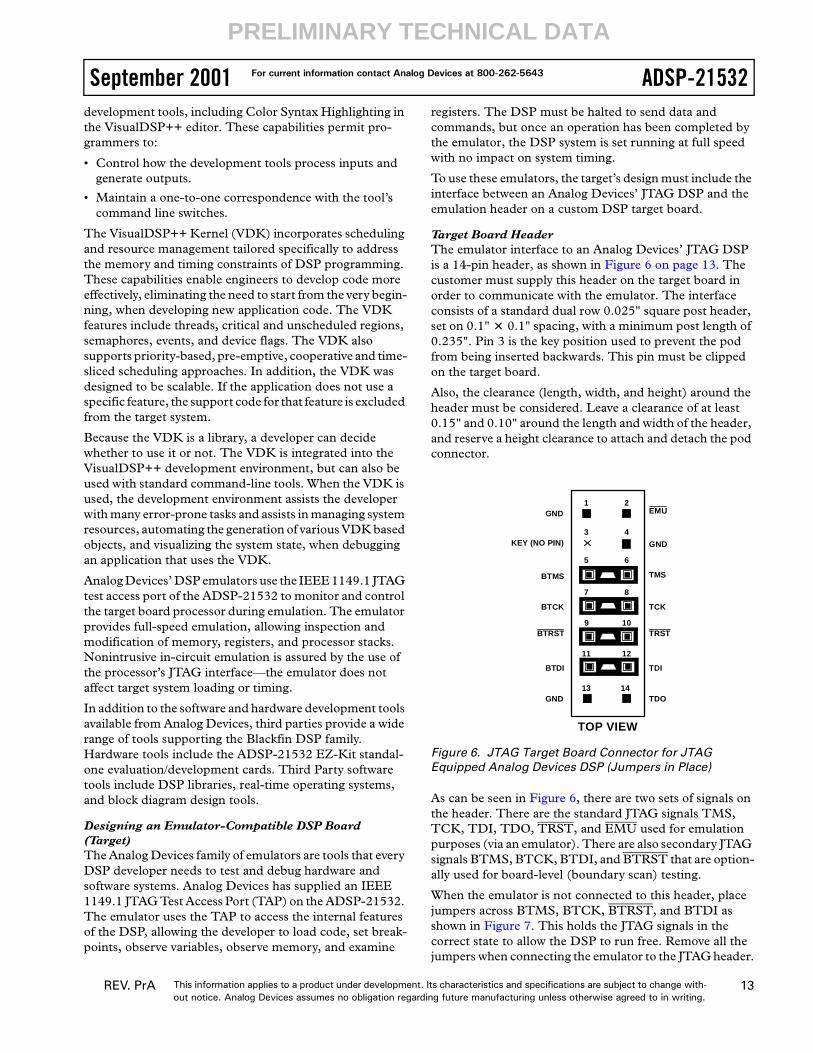
To use these emulators, the target’s design must include the interface between an Analog Devices’ JTAG DSP and the emulation header on a custom DSP target board.
Target Board HeaderThe emulator interface to an Analog Devices’ JTAG DSP is a 14-pin header, as shown in Figure 6 on page 13. The customer must supply this header on the target board in order to communicate with the emulator. The interface consists of a standard dual row 0.025" square post header, set on 0.1" � 0.1" spacing, with a minimum post length of 0.235". Pin 3 is the key position used to prevent the pod from being inserted backwards. This pin must be clipped on the target board.
Also, the clearance (length, width, and height) around the header must be considered. Leave a clearance of at least 0.15" and 0.10" around the length and width of the header, and reserve a height clearance to attach and detach the pod connector.
As can be seen in Figure 6, there are two sets of signals on the header. There are the standard JTAG signals TMS, TCK, TDI, TDO, TRST, and EMU used for emulation purposes (via an emulator). There are also secondary JTAG signals BTMS, BTCK, BTDI, and BTRST that are option-ally used for board-level (boundary scan) testing.
When the emulator is not connected to this header, place jumpers across BTMS, BTCK, BTRST, and BTDI as shown in Figure 7. This holds the JTAG signals in the correct state to allow the DSP to run free. Remove all the jumpers when connecting the emulator to the JTAG header.
Figure 6. JTAG Target Board Connector for JTAG Equipped Analog Devices DSP (Jumpers in Place)
TOP VIEW
13 14
11 12
9 10
9
7 8
5 6
3 4
1 2EMU
GND
TMS
TCK
TRST
TDI
TDO
GND
KEY (NO PIN)
BTMS
BTCK
BTRST
BTDI
GND

For current information contact Analog Devices at 800-262-5643ADSP-21532 September 2001
This information applies to a product under development. Its characteristics and specifications are subject to change with-out notice. Analog Devices assumes no obligation regarding future manufacturing unless otherwise agreed to in writing.
14 REV. PrA
PRELIMINARY TECHNICAL DATA
JTAG Emulator Pod ConnectorFigure 8 details the dimensions of the JTAG pod connector at the 14-pin target end. Figure 9 displays the keep-out area for a target board header. The keep-out area allows the pod connector to properly seat onto the target board header. This board area should contain no components (chips, resistors, capacitors, etc.). The dimensions are referenced to the center of the 0.25" square post pin.
Design-for-Emulation Circuit InformationFor details on target board design issues including: single processor connections, multiprocessor scan chains, signal buffering, signal termination, and emulator pod logic, see the EE-68: Analog Devices JTAG Emulation Technical Reference on the Analog Devices website
(www.analog.com)—use site search on “EE-68”. This document is updated regularly to keep pace with improve-ments to emulator support.
Additional InformationThis data sheet provides a general overview of the ADSP-21532 architecture and functionality. For additional infor-mation on the Blackfin DSP Family core architecture and instruction set, see the Analog Devices’ website.
PIN DESCRIPTIONSADSP-21532 pin definitions are listed in Table 8. The following pins are asynchronous: ARDY, PF15–0, NMI, TRST, RESET, CLKIN, XTAL.
Unused inputs should be tied or pulled to VDDEXT or GND.
The following symbols appear in the Type column of Table 8: I = Input, O = Output, T = Three-State, P = Power, and G = Ground.
Figure 7. JTAG Target Board Connector with No Local Boundary Scan
Figure 8. JTAG Pod Connector Dimensions
Figure 9. JTAG Pod Connector Keep-Out Area
TOP VIEW
13 14
11 12
9 10
9
7 8
5 6
3 4
1 2EMU
GND
TMS
TCK
TRST
TDI
TDO
GND
KEY (NO PIN)
BTMS
BTCK
BTRST
BTDI
GND
0.64"
0.88"
0.24"
0.10"
0.15"
Table 8. Pin Descriptions
Pin Name I/O Function
Memory InterfaceA[19:1] O Address Bus for Async/Sync
AccessD[15:0] I/O Data Bus for Async/Sync
AccessABE /SDQM[1:0]
O Byte Enables/Data Masks for Async/Sync Access
BR I Bus RequestBG O Bus GrantBGH O Bus Grant Hang
Asynchronous Memory ControlAMS3–0 O Bank SelectARDY I Hardware Ready ControlAOE O Output EnableARE O Read EnableAWE O Write Enable
Synchronous Memory ControlSRAS O Row Address StrobeSCAS O Column Address StrobeSWE O Write EnableSCKE O Clock EnableCLKOUT O Clock OutputSA10 O A10 PinSMS O Bank Select
TimersTMR0 I/O Timer 0TMR1 I/O Timer 1TMR2 I/O Timer 2

This information applies to a product under development. Its characteristics and specifications are subject to change with-out notice. Analog Devices assumes no obligation regarding future manufacturing unless otherwise agreed to in writing.
15REV. PrA
For current information contact Analog Devices at 800-262-5643 ADSP-21532September 2001
PRELIMINARY TECHNICAL DATA
Parallel Peripheral Interface PortPF15–0 I/O Programmable Flag Pins/PPIPPICLK I PPI Clock
Serial PortsRSCLK0 I/O Sport0 Receive Serial ClockRFS0 I/O Sport0 Receive Frame SyncDR0PRI I Sport0 Receive Data PrimaryDR0SEC I Sport0 Receive Data
SecondaryTSCLK0 I/O Sport0 Transmit Serial ClockTFS0 I/O Sport0 Transmit Frame SyncDT0PRI O Sport0 Transmit Data
PrimaryDT0SEC O Sport0 Transmit Data
SecondaryRSCLK1 I/O Sport1 Receive Serial ClockRFS1 I/O Sport1 Receive Frame SyncDR1PRI I Sport1 Receive Data PrimaryDR1SEC I Sport1 Receive Data
SecondaryTSCLK1 I/O Sport1 Transmit Serial ClockTFS1 I/O Sport1 Transmit Frame SyncDT1PRI O Sport1 Transmit Data
PrimaryDT1SEC O Sport1 Transmit Data
Secondary
SPI PortMOSI I/O Master Out Slave InMISO I/O Master In Slave OutSCK I/O Clock
UART PortRX I UART ReceiveTX O UART Transmit
Real Time ClockRTXI I RTC Crystal InputRTXO O RTC Crystal Output
JTAG PortTCK I JTAG ClockTDO O JTAG Serial Data OutTDI I JTAG Serial Data InTMS I JTAG Mode SelectTRST I JTAG ResetEMU O Emulation Output
ClockCLKIN I Clock/Crystal InputXTAL O Crystal Output
Table 8. Pin Descriptions (Continued)
Pin Name I/O Function
Mode ControlsRESET I ResetNMI I Non-maskable InterruptBMODE2–0 I Boot Mode Strap
Voltage RegulatorVDDCRTL O External FET/BJT DriveVREFFLT I Voltage Reference Filter
SuppliesVDDEXT P I/O Power Supply
(3.3 V nominal)VDDINT P Internal Power Supply
(regulated from 2.25 V to 3.6 V)
VDDRTC P Real Time Clock Power Supply (3.3 V Nominal)
GND G External Ground
Table 8. Pin Descriptions (Continued)
Pin Name I/O Function
For current information contact Analog Devices at 800-262-5643ADSP-21532 September 2001
This information applies to a product under development. Its characteristics and specifications are subject to change with-out notice. Analog Devices assumes no obligation regarding future manufacturing unless otherwise agreed to in writing.
16 REV. PrA
PRELIMINARY TECHNICAL DATA
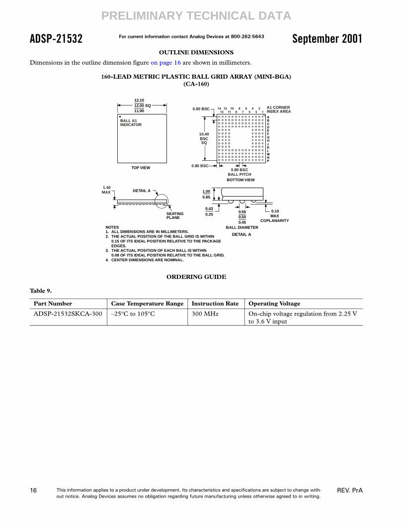
OUTLINE DIMENSIONS
Dimensions in the outline dimension figure on page 16 are shown in millimeters.
ORDERING GUIDE
160-LEAD METRIC PLASTIC BALL GRID ARRAY (MINI-BGA)(CA-160)
Table 9.
Part Number Case Temperature Range Instruction Rate Operating Voltage
ADSP-21532SKCA-300 –25ºC to 105ºC 300 MHz On-chip voltage regulation from 2.25 V to 3.6 V input
TOP VIEW
12.1012.00 SQ11.90
BALL A1INDICATOR
DETAIL A
SEATINGPLANE
1.40MAX
0.430.25
0.550.500.45
BALL DIAMETER
DETAIL A
1.000.85
BOTTOM VIEW
ABCDEFGHJKLMNP
13 11 9 7 5 3 114 12 10 8 6 4 2
0.80 BSCBALL PITCH
10.40BSCSQ
0.80 BSC
NOTES1. ALL DIMENSIONS ARE IN MILLIMETERS.2. THE ACTUAL POSITION OF THE BALL GRID IS WITHIN
0.15 OF ITS IDEAL POSITION RELATIVE TO THE PACKAGEEDGES.
3. THE ACTUAL POSITION OF EACH BALL IS WITHIN0.08 OF ITS IDEAL POSITION RELATIVE TO THE BALL GRID.
4. CENTER DIMENSIONS ARE NOMINAL.
A1 CORNERINDEX AREA
0.10MAX
COPLANARITY
0.80 BSC