primecell dma controller (pl080) - arm...
TRANSCRIPT
PrimeCell® DMA Controller (PL080)Revision: r1p3
Technical Reference Manual
Copyright © 2000-2001, 2003-2005 ARM Limited. All rights reserved.ARM DDI 0196G
PrimeCell DMA Controller (PL080)Technical Reference Manual
Copyright © 2000-2001, 2003-2005 ARM Limited. All rights reserved.
Release Information
The following changes have been made to this document.
Proprietary Notice
Words and logos marked with ® or ™ are registered trademarks or trademarks of ARM Limited in the EU and other countries, except as otherwise stated below in this proprietary notice. Other brands and names mentioned herein may be the trademarks of their respective owners.
Neither the whole nor any part of the information contained in, or the product described in, this document may be adapted or reproduced in any material form except with the prior written permission of the copyright holder.
The product described in this document is subject to continuous developments and improvements. All particulars of the product and its use contained in this document are given by ARM Limited in good faith. However, all warranties implied or expressed, including but not limited to implied warranties of merchantability, or fitness for purpose, are excluded.
This document is intended only to assist the reader in the use of the product. ARM Limited shall not be liable for any loss or damage arising from the use of any information in this document, or any error or omission in such information, or any incorrect use of the product.
Confidentiality Status
This document is Non-Confidential. The right to use, copy and disclose this document may be subject to license restrictions in accordance with the terms of the agreement entered into by ARM and the party that ARM delivered this document to.
Change history
Date Issue Confidentiality Change
November 2000 A Non-Confidential First issue, release 1v0.
April 2001 B Non-Confidential Second issue, release 1v0.
July 2001 C Non-Confidential Third issue, release 1v0.
January 2003 D Non-Confidential Incorporation of errata, clarification of endian behavior, and addition of software considerations for release r1p1.
November 2003 E Non-Confidential Changes for r1p2. Incorporation of errata.
31 August 2004 F Non-Confidential First issue for r1p3.
20 December 2005 G Non-Confidential Incorporation of errata, corrected bit descriptions in Integration Test Output Register 3 on page 4-6.
ii Copyright © 2000-2001, 2003-2005 ARM Limited. All rights reserved. ARM DDI 0196G
Product Status
The information in this document is final, that is for a developed product.
Web Address
http://www.arm.com
ARM DDI 0196G Copyright © 2000-2001, 2003-2005 ARM Limited. All rights reserved. iii

iv Copyright © 2000-2001, 2003-2005 ARM Limited. All rights reserved. ARM DDI 0196G
ContentsPrimeCell DMA Controller (PL080) Technical Reference Manual
PrefaceAbout this manual ........................................................................................ xivFeedback ................................................................................................... xviii
Chapter 1 Introduction1.1 About the DMAC ......................................................................................... 1-21.2 Product revisions ........................................................................................ 1-4
Chapter 2 Functional Overview2.1 Functional description ................................................................................. 2-22.2 System considerations .............................................................................. 2-122.3 System connectivity .................................................................................. 2-132.4 Software considerations ............................................................................ 2-182.5 Use with memory management unit based systems ................................. 2-21
Chapter 3 Programmer’s Model3.1 About the programmer’s model ................................................................... 3-23.2 Programming the DMAC ............................................................................. 3-33.3 Summary of registers .................................................................................. 3-63.4 Register descriptions ................................................................................ 3-10
ARM DDI 0196G Copyright © 2000-2001, 2003-2005 ARM Limited. All rights reserved. v
Contents
3.5 Address generation .................................................................................. 3-373.6 Scatter/gather ........................................................................................... 3-383.7 Interrupt requests ..................................................................................... 3-403.8 DMAC data flow ........................................................................................ 3-43
Chapter 4 Programmer’s Model for Test4.1 DMAC test harness overview ..................................................................... 4-24.2 Scan testing ................................................................................................ 4-34.3 Test registers .............................................................................................. 4-44.4 Integration test ............................................................................................ 4-7
Appendix A Signal DescriptionsA.1 DMA interrupt request signals .................................................................... A-2A.2 DMA request and response signals ............................................................ A-3A.3 AHB slave signals ....................................................................................... A-4A.4 AHB master signals .................................................................................... A-6A.5 AHB master bus request signals ................................................................ A-8A.6 Scan test control signals ............................................................................. A-9
Appendix B DMA InterfaceB.1 DMA request signals .................................................................................. B-2B.2 DMA response signals ................................................................................ B-3B.3 Flow control ................................................................................................ B-4B.4 Transfer types ............................................................................................. B-5B.5 Signal timing ............................................................................................. B-17B.6 Functional timing diagram ........................................................................ B-18B.7 DMAC transfer timing diagram ................................................................. B-19
Appendix C Scatter/GatherC.1 Scatter/gather through linked list operation ................................................ C-2
Glossary
vi Copyright © 2000-2001, 2003-2005 ARM Limited. All rights reserved. ARM DDI 0196G
List of TablesPrimeCell DMA Controller (PL080) Technical Reference Manual
Change history .............................................................................................................. iiTable 2-1 Endian behavior ........................................................................................................ 2-5Table 3-1 Register summary ..................................................................................................... 3-6Table 3-2 DMACIntStatus Register bit assignments ............................................................... 3-10Table 3-3 DMACIntTCStatus Register bit assignments .......................................................... 3-11Table 3-4 DMACIntTCClear Register bit assignments ............................................................ 3-11Table 3-5 DMACIntErrorStatus Register bit assignments ....................................................... 3-12Table 3-6 DMACIntErrClr Register bit assignments ................................................................ 3-12Table 3-7 DMACRawIntTCStatus Register bit assignments ................................................... 3-13Table 3-8 DMACRawIntErrorStatus Register bit assignments ................................................ 3-13Table 3-9 DMACEnbldChns Register bit assignments ............................................................ 3-14Table 3-10 DMACSoftBReq Register bit assignments .............................................................. 3-15Table 3-11 DMACSoftSReq Register bit assignments .............................................................. 3-15Table 3-12 DMACSoftLBReq Register bit assignments ............................................................ 3-16Table 3-13 DMACSoftLSReq Register bit assignments ............................................................ 3-17Table 3-14 DMACConfiguration Register bit assignments ........................................................ 3-18Table 3-15 DMACSync Register bit assignments ..................................................................... 3-20Table 3-16 DMACCxSrcAddr Register bit assignments ............................................................ 3-21Table 3-17 DMACCxDestAddr Register bit assignments .......................................................... 3-22Table 3-18 DMACCxLLI Register bit assignments .................................................................... 3-22Table 3-19 DMACCxControl Register bit assignments ............................................................. 3-23
ARM DDI 0196G Copyright © 2000-2001, 2003-2005 ARM Limited. All rights reserved. vii
List of Tables
Table 3-20 Source or destination burst size ............................................................................. 3-25Table 3-21 Source or destination transfer width ....................................................................... 3-25Table 3-22 Protection bits ......................................................................................................... 3-26Table 3-23 DMACCxConfiguration Register bit assignments ................................................... 3-27Table 3-24 Flow control and transfer type bits .......................................................................... 3-29Table 3-25 DMACPeriphID0 Register bit assignments ............................................................. 3-30Table 3-26 DMACPeriphID1 Register bit assignments ............................................................. 3-31Table 3-27 DMACPeriphID2 Register bit assignments ............................................................. 3-32Table 3-28 DMACPeriphID3 Register bit assignments ............................................................. 3-33Table 3-29 DMACPCellID0 Register bit assignments ............................................................... 3-35Table 3-30 DMACPCellID1 Register bit assignments ............................................................... 3-35Table 3-31 DMACPCellID2 Register bit assignments ............................................................... 3-36Table 3-32 DMACPCellID3 Register bit assignments ............................................................... 3-36Table 4-1 DMACITCR Register bit assignments ...................................................................... 4-4Table 4-2 DMACITOP1 Register bit assignments .................................................................... 4-5Table 4-3 DMACITOP2 Register bit assignments .................................................................... 4-5Table 4-4 DMACITOP3 Register bit assignments .................................................................... 4-6Table A-1 DMA interrupt request signal descriptions ................................................................ A-2Table A-2 DMA request and response signal descriptions ....................................................... A-3Table A-3 AHB slave signal descriptions .................................................................................. A-4Table A-4 AHB master signal descriptions ................................................................................ A-6Table A-5 AHB master bus request signal descriptions ............................................................ A-8Table A-6 Internal scan test control signal descriptions ............................................................ A-9Table B-1 DMA request signal usage ........................................................................................ B-5
viii Copyright © 2000-2001, 2003-2005 ARM Limited. All rights reserved. ARM DDI 0196G
List of FiguresPrimeCell DMA Controller (PL080) Technical Reference Manual
Key to timing diagram conventions ............................................................................ xviFigure 2-1 DMAC block diagram ................................................................................................ 2-2Figure 2-2 Dual AHB masters ..................................................................................................... 2-4Figure 2-3 DMAC connectivity .................................................................................................. 2-13Figure 2-4 Connection for higher performance systems .......................................................... 2-16Figure 2-5 Connection for lower performance systems ............................................................ 2-16Figure 2-6 Complex example of connectivity ............................................................................ 2-17Figure 2-7 Simple example of connectivity ............................................................................... 2-17Figure 3-1 DMACIntStatus Register bit assignments ............................................................... 3-10Figure 3-2 DMACIntTCStatus Register bit assignments .......................................................... 3-10Figure 3-3 DMACIntTCClear Register bit assignments ............................................................ 3-11Figure 3-4 DMACIntErrorStatus Register bit assignments ....................................................... 3-12Figure 3-5 DMACIntErrorStatus Register bit assignments ....................................................... 3-12Figure 3-6 DMACRawIntTCStatus Register bit assignments ................................................... 3-13Figure 3-7 DMACRawIntErrorStatus Register bit assignments ................................................ 3-13Figure 3-8 DMACEnbldChns Register bit assignments ............................................................ 3-14Figure 3-9 DMACSoftBReq Register bit assignments .............................................................. 3-14Figure 3-10 DMACSoftSReq Register bit assignments .............................................................. 3-15Figure 3-11 DMACSoftLBReq Register bit assignments ............................................................ 3-16Figure 3-12 DMACSoftLSReq Register bit assignments ............................................................ 3-16Figure 3-13 DMACConfiguration Register bit assignments ........................................................ 3-18
ARM DDI 0196G Copyright © 2000-2001, 2003-2005 ARM Limited. All rights reserved. ix
List of Figures
Figure 3-14 DMACSync Register bit assignments ..................................................................... 3-20Figure 3-15 DMACCxLLI Register bit assignments ................................................................... 3-22Figure 3-16 DMACCxControl Register bit assignments ............................................................. 3-23Figure 3-17 DMACCxConfiguration Register bit assignments ................................................... 3-27Figure 3-18 Peripheral Identification Register bit assignments .................................................. 3-30Figure 3-19 DMACPeriphID0 Register bit assignments ............................................................. 3-30Figure 3-20 DMACPeriphID1 Register bit assignments ............................................................. 3-31Figure 3-21 DMACPeriphID2 Register bit assignments ............................................................. 3-31Figure 3-22 DMACPeriphID3 Register bit assignments ............................................................. 3-32Figure 3-23 PrimeCell Identification Register bit assignments ................................................... 3-34Figure 3-24 DMACPCellID0 Register bit assignments ............................................................... 3-35Figure 3-25 DMACPCellID1 Register bit assignments ............................................................... 3-35Figure 3-26 DMACPCellID2 Register bit assignments ............................................................... 3-36Figure 3-27 DMACPCellID3 Register bit assignments ............................................................... 3-36Figure 4-1 DMACITCR Register bit assignments ...................................................................... 4-4Figure 4-2 DMACITOP1 Register bit assignments .................................................................... 4-5Figure 4-3 DMACITOP2 Register bit assignments .................................................................... 4-5Figure 4-4 DMACITOP3 Register bit assignments .................................................................... 4-6Figure B-1 Peripheral-to-memory transaction comprising bursts ............................................... B-6Figure B-2 Peripheral-to-memory transaction comprising single requests ................................. B-6Figure B-3 Peripheral-to-memory transaction comprising bursts and single requests ............... B-6Figure B-4 Memory-to-peripheral transaction comprising bursts ................................................ B-7Figure B-5 Memory-to-peripheral transaction comprising single requests ................................. B-7Figure B-6 Memory-to-peripheral transaction comprising bursts that are not multiples of the burst
size ........................................................................................................................... B-7Figure B-7 Memory-to-memory transaction under DMA flow control ......................................... B-8Figure B-8 Peripheral-to-peripheral transaction comprising bursts ............................................ B-8Figure B-9 Peripheral-to-peripheral transaction comprising single transfers .............................. B-9Figure B-10 Peripheral-to-peripheral transaction comprising bursts and single requests ............ B-9Figure B-11 Memory-to-peripheral transaction under peripheral flow control comprising bursts . B-9Figure B-12 Memory-to-peripheral transaction under peripheral flow control comprising single trans-
fers .......................................................................................................................... B-10Figure B-13 Memory-to-peripheral transaction under peripheral flow control comprising bursts and
single transfers ....................................................................................................... B-10Figure B-14 Peripheral-to-memory transaction under peripheral flow control comprising bursts B-11Figure B-15 Peripheral-to-memory transaction under peripheral flow control comprising single trans-
fers .......................................................................................................................... B-11Figure B-16 Peripheral-to-memory transaction under peripheral flow control comprising bursts and
single transfers ....................................................................................................... B-11Figure B-17 Peripheral-to-peripheral transaction under source peripheral flow control comprising
bursts ...................................................................................................................... B-12Figure B-18 Peripheral-to-peripheral transaction under source peripheral flow control comprising sin-
gle transfers ............................................................................................................ B-13Figure B-19 Peripheral-to-peripheral transaction under source peripheral flow control comprising
bursts and single transfers ...................................................................................... B-13Figure B-20 Peripheral-to-peripheral transaction under destination peripheral flow control comprising
bursts ...................................................................................................................... B-14
x Copyright © 2000-2001, 2003-2005 ARM Limited. All rights reserved. ARM DDI 0196G
List of Figures
Figure B-21 Peripheral-to-peripheral transaction under destination peripheral flow control comprising single transfers ........................................................................................................ B-14
Figure B-22 Peripheral-to-peripheral transaction under destination peripheral flow control comprising bursts and single transfers ...................................................................................... B-15
Figure B-23 DMA interface timing ............................................................................................... B-18Figure B-24 DMAC transfer timing diagram ................................................................................ B-19Figure C-1 LLI example .............................................................................................................. C-2
ARM DDI 0196G Copyright © 2000-2001, 2003-2005 ARM Limited. All rights reserved. xi
List of Figures
xii Copyright © 2000-2001, 2003-2005 ARM Limited. All rights reserved. ARM DDI 0196G
Preface
This preface introduces the ARM PrimeCell DMA Controller (PL080) Technical Reference Manual. It contains the following sections:
• About this manual on page xiv
• Feedback on page xviii.
ARM DDI 0196G Copyright © 2000-2001, 2003-2005 ARM Limited. All rights reserved. xiii
Preface
About this manual
This is the Technical Reference Manual (TRM) for the ARM PrimeCell DMA Controller (PL080) (DMAC).
Product revision status
The rnpn identifier indicates the revision status of the product described in this manual, where:
rn Identifies the major revision of the product.
pn Identifies the minor revision or modification status of the product.
Intended audience
This manual is written for hardware and software engineers implementing System-on-Chip (SoC) designs. It provides information to enable designers to integrate the peripheral into a target system as quickly as possible. The manual describes the external functionality of the DMAC.
Using this manual
This manual is organized into the following chapters:
Chapter 1 Introduction
Read this chapter for an introduction to the ARM DMAC.
Chapter 2 Functional Overview
Read this chapter for a description of the major functional blocks of the DMAC.
Chapter 3 Programmer’s Model
Read this chapter for a description of the DMAC registers and programming details.
Chapter 4 Programmer’s Model for Test
Read this chapter for a description of how to use the logic in the DMAC for functional verification and production testing.
xiv Copyright © 2000-2001, 2003-2005 ARM Limited. All rights reserved. ARM DDI 0196G
Preface
Appendix A Signal Descriptions
Read this appendix for descriptions of the DMAC signals.
Appendix B DMA Interface
Read this appendix for a description of how to use the DMAC request and response interface.
Appendix C Scatter/Gather
Read this appendix for a description of scatter/gather through Linked List Items (LLIs).
Glossary Read the Glossary for definitions of terms used in this manual.
Conventions
Conventions that this manual can use are described in:
• Typographical
• Timing diagrams on page xvi
• Signals on page xvi
• Numbering on page xvii.
Typographical
The typographical conventions are:
italic Highlights important notes, introduces special terminology, denotes internal cross-references, and citations.
bold Highlights interface elements, such as menu names. Denotes signal names. Also used for terms in descriptive lists, where appropriate.
monospace Denotes text that you can enter at the keyboard, such as commands, file and program names, and source code.
monospace Denotes a permitted abbreviation for a command or option. You can enter the underlined text instead of the full command or option name.
monospace italic Denotes arguments to monospace text where the argument is to be replaced by a specific value.
monospace bold Denotes language keywords when used outside example code.
ARM DDI 0196G Copyright © 2000-2001, 2003-2005 ARM Limited. All rights reserved. xv
Preface
< and > Angle brackets enclose replaceable terms for assembler syntax where they appear in code or code fragments. They appear in normal font in running text. For example:
• MRC p15, 0 <Rd>, <CRn>, <CRm>, <Opcode_2>
• The Opcode_2 value selects which register is accessed.
Timing diagrams
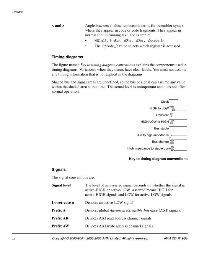
The figure named Key to timing diagram conventions explains the components used in timing diagrams. Variations, when they occur, have clear labels. You must not assume any timing information that is not explicit in the diagrams.
Shaded bus and signal areas are undefined, so the bus or signal can assume any value within the shaded area at that time. The actual level is unimportant and does not affect normal operation.
Key to timing diagram conventions
Signals
The signal conventions are:
Signal level The level of an asserted signal depends on whether the signal is active-HIGH or active-LOW. Asserted means HIGH for active-HIGH signals and LOW for active-LOW signals.
Lower-case n Denotes an active-LOW signal.
Prefix A Denotes global Advanced eXtensible Interface (AXI) signals:
Prefix AR Denotes AXI read address channel signals.
Prefix AW Denotes AXI write address channel signals.
xvi Copyright © 2000-2001, 2003-2005 ARM Limited. All rights reserved. ARM DDI 0196G
Preface
Prefix B Denotes AXI write response channel signals.
Prefix C Denotes AXI low-power interface signals.
Prefix H Denotes Advanced High-performance Bus (AHB) signals.
Prefix P Denotes Advanced Peripheral Bus (APB) signals.
Prefix R Denotes AXI read data channel signals.
Prefix W Denotes AXI write data channel signals.
Suffix n AHB HRESETn and APB PRESETn reset signals.
Numbering
The numbering convention is:
<size in bits>'<base><number>
This is a Verilog method of abbreviating constant numbers. For example:
• 'h7B4 is an unsized hexadecimal value.
• 'o7654 is an unsized octal value.
• 8'd9 is an eight-bit wide decimal value of 9.
• 8'h3F is an eight-bit wide hexadecimal value of 0x3F. This is equivalent to b00111111.
• 8'b1111 is an eight-bit wide binary value of b00001111.
Further reading
This section lists publications by ARM Limited, and by third parties.
ARM Limited periodically provides updates and corrections to its documentation. See http://www.arm.com for current errata sheets, addenda, and the Frequently Asked Questions list.
ARM publications
This manual contains information that is specific to the DMAC (PL080). See the following documents for other relevant information:
• AMBA® Specification (Rev 2.0) (ARM IHI 0011)
• ARM PrimeCell DMA Controller (PL080) Design Manual (PL080 DDES 0000)
• ARM PrimeCell DMA Controller (PL080) Integration Manual (PL080 INTM 0000).
ARM DDI 0196G Copyright © 2000-2001, 2003-2005 ARM Limited. All rights reserved. xvii
Preface
Feedback
ARM Limited welcomes feedback on the DMAC (PL080) and its documentation.
Feedback on this product
If you have any comments or suggestions about this product, contact your supplier giving:
• the product name
• a concise explanation of your comments.
Feedback on this manual
If you have any comments on this manual, send email to [email protected] giving:
• the title
• the number
• the relevant page number(s) to which your comments apply
• a concise explanation of your comments.
ARM Limited also welcomes general suggestions for additions and improvements.
xviii Copyright © 2000-2001, 2003-2005 ARM Limited. All rights reserved. ARM DDI 0196G
Chapter 1 Introduction
This chapter introduces the PrimeCell DMA Controller (DMAC). It contains the following sections:
• About the DMAC on page 1-2
• Product revisions on page 1-4.
ARM DDI 0196G Copyright © 2000-2001, 2003-2005 ARM Limited. All rights reserved. 1-1
Introduction
1.1 About the DMAC
The DMAC is an Advanced Microcontroller Bus Architecture (AMBA) compliant System-on-Chip (SoC) peripheral that is developed, tested, and licensed by ARM Limited.
The DMAC is an AMBA AHB module, and connects to the Advanced High-performance Bus (AHB).
1.1.1 Features of the DMAC
The DMAC offers:
• Compliance to the AMBA Specification for easy integration into SoC implementation.
• Eight DMA channels. Each channel can support a unidirectional transfer.
• 16 DMA requests. The DMAC provides 16 peripheral DMA request lines.
• Single DMA and burst DMA request signals. Each peripheral connected to the DMAC can assert either a burst DMA request or a single DMA request. You set the DMA burst size by programming the DMAC.
• Memory-to-memory, memory-to-peripheral, peripheral-to-memory, and peripheral-to-peripheral transfers.
• Scatter or gather DMA support through the use of linked lists.
• Hardware DMA channel priority. Each DMA channel has a specific hardware priority. DMA channel 0 has the highest priority and channel 7 has the lowest priority. If requests from two channels become active at the same time, the channel with the highest priority is serviced first.
• AHB slave DMA programming interface. You program the DMAC by writing to the DMA control registers over the AHB slave interface.
• Two AHB bus masters for transferring data. Use these interfaces to transfer data when a DMA request goes active.
• 32-bit AHB master bus width.
• Incrementing or non-incrementing addressing for source and destination.
• Programmable DMA burst size. You can programme the DMA burst size to transfer data more efficiently. The burst size is usually set to half the size of the FIFO in the peripheral.
1-2 Copyright © 2000-2001, 2003-2005 ARM Limited. All rights reserved. ARM DDI 0196G
Introduction
• Internal four word FIFO per channel.
• Supports eight, 16, and 32-bit wide transactions.
• Big-endian and little-endian support. The DMAC defaults to little-endian mode on reset.
• Separate and combined DMA error and DMA count interrupt requests. You can generate an interrupt to the processor on a DMA error or when a DMA count has reached 0. This is usually used to indicate that a transfer has finished. There are three interrupt request signals to do this:
— DMACINTTC signals when a transfer has completed.
— DMACINTERR signals when an error has occurred.
— DMACINTR combines both the DMACINTTC and DMACINTERR interrupt request signals. You can use the DMACINTR interrupt request in systems that have few interrupt controller request inputs.
• Interrupt masking. You can mask the DMA error and DMA terminal count interrupt requests.
• Raw interrupt status. You can read the DMA error and DMA count raw interrupt status prior to masking.
• Test registers for use in block and integration system level testing.
• Identification registers that uniquely identify the DMAC. An operating system can use these to automatically configure itself.
ARM DDI 0196G Copyright © 2000-2001, 2003-2005 ARM Limited. All rights reserved. 1-3
Introduction
1.2 Product revisions
This section describes differences in functionality between product revisions of the DMAC (PL080):
Rel 1v0 - r1p1
Contains the following differences in functionality:
• correction of endianness behavior
• addition of new AHBLite Master
• improvement in performance.
r1p1 - r1p2 The DMACPeriphID2 Register Revision bit field is updated.
r1p2 - r1p3 The LLI loading update is corrected. This does not affect the information provided in this manual.
1-4 Copyright © 2000-2001, 2003-2005 ARM Limited. All rights reserved. ARM DDI 0196G
Chapter 2 Functional Overview
This chapter describes the major functional blocks of the DMAC. It contains the following sections:
• Functional description on page 2-2
• System considerations on page 2-12
• System connectivity on page 2-13
• Software considerations on page 2-18
• Use with memory management unit based systems on page 2-21.
ARM DDI 0196G Copyright © 2000-2001, 2003-2005 ARM Limited. All rights reserved. 2-1
Functional Overview
2.1 Functional description
The DMAC enables the following transactions:
• memory-to-memory
• memory-to-peripheral
• peripheral-to-memory
• peripheral-to-peripheral.
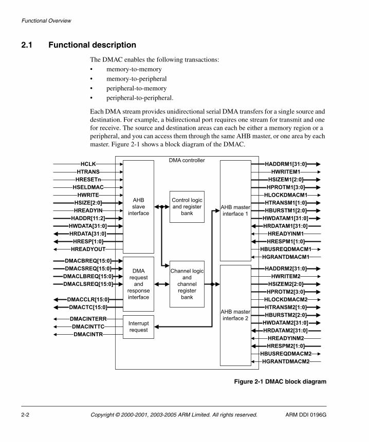
Each DMA stream provides unidirectional serial DMA transfers for a single source and destination. For example, a bidirectional port requires one stream for transmit and one for receive. The source and destination areas can each be either a memory region or a peripheral, and you can access them through the same AHB master, or one area by each master. Figure 2-1 shows a block diagram of the DMAC.
Figure 2-1 DMAC block diagram
2-2 Copyright © 2000-2001, 2003-2005 ARM Limited. All rights reserved. ARM DDI 0196G
Functional Overview
Note For clarity, Figure 2-1 on page 2-2 does not show test logic.
The following sections describe the functions of the DMAC:
• AHB slave interface
• Control logic and register bank
• DMA request and response interface
• Channel logic and channel register bank
• Interrupt request
• AHB master interfaces on page 2-4
• Channel hardware on page 2-11
• Test registers on page 2-11
• DMA request priority on page 2-11.
2.1.1 AHB slave interface
All transactions on the AHB slave programming bus of the DMAC are 32 bits. This eliminates endian issues when programming the DMAC.
2.1.2 Control logic and register bank
The register block stores data written, or to be read across the AMBA AHB interface. Program the DMAC with this block using an AMBA AHB slave interface.
2.1.3 DMA request and response interface
See Appendix B DMA Interface for information on the DMA request and response interface.
2.1.4 Channel logic and channel register bank
The channel logic and channel register bank contains registers and logic that each DMA channel requires.
2.1.5 Interrupt request
The interrupt request generates interrupts to the ARM processor.
ARM DDI 0196G Copyright © 2000-2001, 2003-2005 ARM Limited. All rights reserved. 2-3
Functional Overview
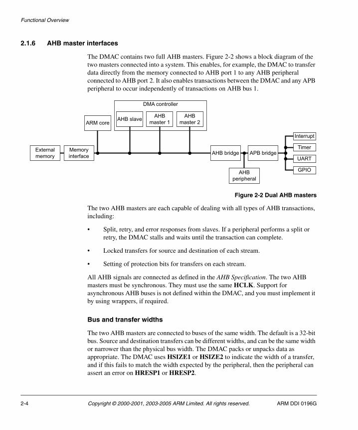
2.1.6 AHB master interfaces
The DMAC contains two full AHB masters. Figure 2-2 shows a block diagram of the two masters connected into a system. This enables, for example, the DMAC to transfer data directly from the memory connected to AHB port 1 to any AHB peripheral connected to AHB port 2. It also enables transactions between the DMAC and any APB peripheral to occur independently of transactions on AHB bus 1.
Figure 2-2 Dual AHB masters
The two AHB masters are each capable of dealing with all types of AHB transactions, including:
• Split, retry, and error responses from slaves. If a peripheral performs a split or retry, the DMAC stalls and waits until the transaction can complete.
• Locked transfers for source and destination of each stream.
• Setting of protection bits for transfers on each stream.
All AHB signals are connected as defined in the AHB Specification. The two AHB masters must be synchronous. They must use the same HCLK. Support for asynchronous AHB buses is not defined within the DMAC, and you must implement it by using wrappers, if required.
Bus and transfer widths
The two AHB masters are connected to buses of the same width. The default is a 32-bit bus. Source and destination transfers can be different widths, and can be the same width or narrower than the physical bus width. The DMAC packs or unpacks data as appropriate. The DMAC uses HSIZE1 or HSIZE2 to indicate the width of a transfer, and if this fails to match the width expected by the peripheral, then the peripheral can assert an error on HRESP1 or HRESP2.
2-4 Copyright © 2000-2001, 2003-2005 ARM Limited. All rights reserved. ARM DDI 0196G
Functional Overview
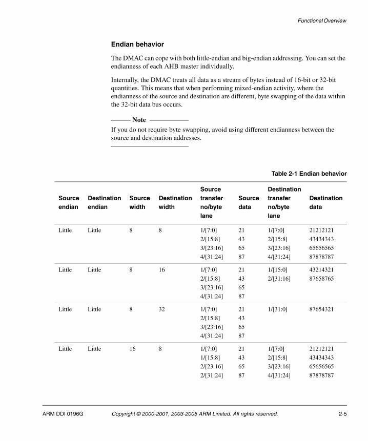
Endian behavior
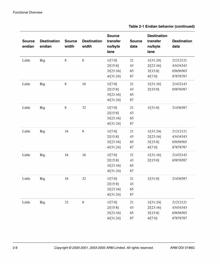
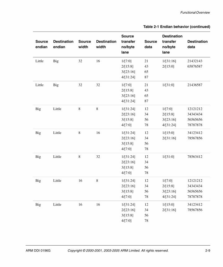
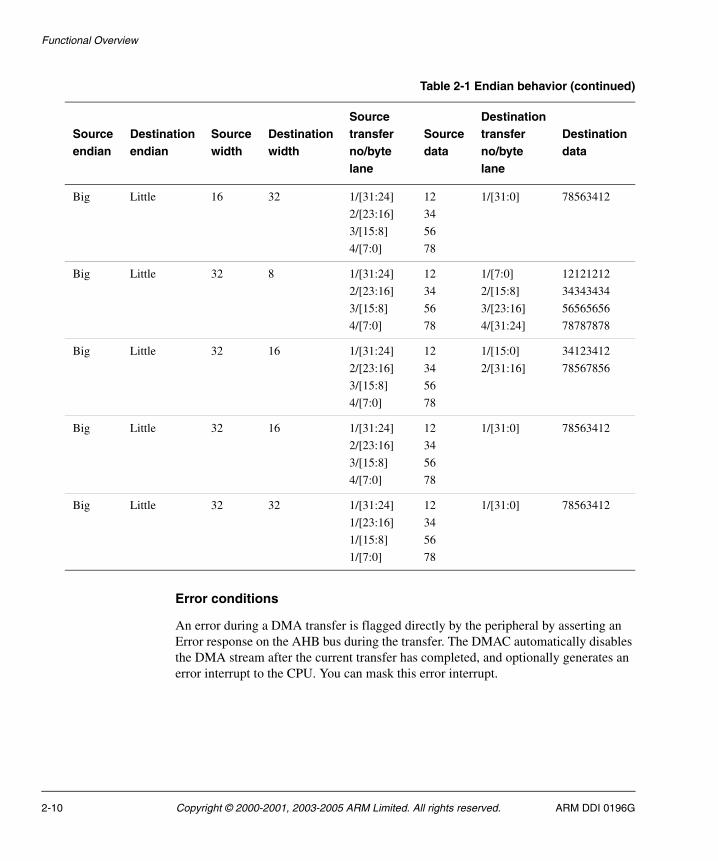
The DMAC can cope with both little-endian and big-endian addressing. You can set the endianness of each AHB master individually.
Internally, the DMAC treats all data as a stream of bytes instead of 16-bit or 32-bit quantities. This means that when performing mixed-endian activity, where the endianness of the source and destination are different, byte swapping of the data within the 32-bit data bus occurs.
Note If you do not require byte swapping, avoid using different endianness between the source and destination addresses.
Table 2-1 Endian behavior
Sourceendian
Destinationendian
Sourcewidth
Destinationwidth
Sourcetransferno/bytelane
Sourcedata
Destinationtransferno/bytelane
Destinationdata
Little Little 8 8 1/[7:0]
2/[15:8]
3/[23:16]
4/[31:24]
21
43
65
87
1/[7:0]
2/[15:8]
3/[23:16]
4/[31:24]
21212121
43434343
65656565
87878787
Little Little 8 16 1/[7:0]
2/[15:8]
3/[23:16]
4/[31:24]
21
43
65
87
1/[15:0]
2/[31:16]
43214321
87658765
Little Little 8 32 1/[7:0]
2/[15:8]
3/[23:16]
4/[31:24]
21
43
65
87
1/[31:0] 87654321
Little Little 16 8 1/[7:0]
1/[15:8]
2/[23:16]
2/[31:24]
21
43
65
87
1/[7:0]
2/[15:8]
3/[23:16]
4/[31:24]
21212121
43434343
65656565
87878787
ARM DDI 0196G Copyright © 2000-2001, 2003-2005 ARM Limited. All rights reserved. 2-5
Functional Overview
Little Little 16 16 1/[7:0]
1/[15:8]
2/[23:16]
2/[31:24]
21
43
65
87
1/[15:0]
2/[31:16]
43214321
87658765
Little Little 16 32 1/[7:0]
1/[15:8]
2/[23:16]
2/[31:24]
21
43
65
87
1/[31:0] 87654321
Little Little 32 8 1/[7:0]
1/[15:8]
1/[23:16]
1/[31:24]
21
43
65
87
1/[7:0]
2/[15:8]
3/[23:16]
4/[31:24]
21212121
43434343
65656565
87878787
Little Little 32 16 1/[7:0]
1/[15:8]
1/[23:16]
1/[31:24]
21
43
65
87
1/[15:0]
2/[31:16]
43214321
87658765
Little Little 32 32 1/[7:0]
1/[15:8]
1/[23:16]
1/[31:24]
21
43
65
87
1/[31:0] 87654321
Big Big 8 8 1/[31:24]
2/[23:16]
3/[15:8]
4/[7:0]
12
34
56
78
1/[31:24]
2/[23:16]
3/[15:8]
4/[7:0]
12121212
34343434
56565656
78787878
Big Big 8 16 1/[31:24]
2/[23:16]
3/[15:8]
4/[7:0]
12
34
56
78
1/[15:0]
2/[31:16]
12341234
56785678
Table 2-1 Endian behavior (continued)
Sourceendian
Destinationendian
Sourcewidth
Destinationwidth
Sourcetransferno/bytelane
Sourcedata
Destinationtransferno/bytelane
Destinationdata
2-6 Copyright © 2000-2001, 2003-2005 ARM Limited. All rights reserved. ARM DDI 0196G
Functional Overview
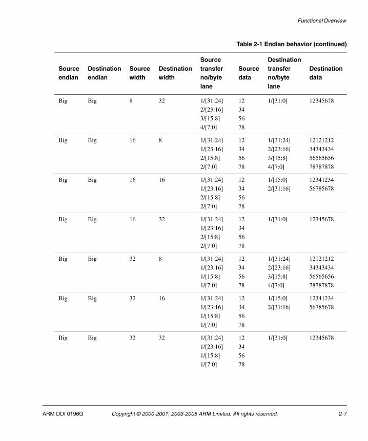
Big Big 8 32 1/[31:24]
2/[23:16]
3/[15:8]
4/[7:0]
12
34
56
78
1/[31:0] 12345678
Big Big 16 8 1/[31:24]
1/[23:16]
2/[15:8]
2/[7:0]
12
34
56
78
1/[31:24]
2/[23:16]
3/[15:8]
4/[7:0]
12121212
34343434
56565656
78787878
Big Big 16 16 1/[31:24]
1/[23:16]
2/[15:8]
2/[7:0]
12
34
56
78
1/[15:0]
2/[31:16]
12341234
56785678
Big Big 16 32 1/[31:24]
1/[23:16]
2/[15:8]
2/[7:0]
12
34
56
78
1/[31:0] 12345678
Big Big 32 8 1/[31:24]
1/[23:16]
1/[15:8]
1/[7:0]
12
34
56
78
1/[31:24]
2/[23:16]
3/[15:8]
4/[7:0]
12121212
34343434
56565656
78787878
Big Big 32 16 1/[31:24]
1/[23:16]
1/[15:8]
1/[7:0]
12
34
56
78
1/[15:0]
2/[31:16]
12341234
56785678
Big Big 32 32 1/[31:24]
1/[23:16]
1/[15:8]
1/[7:0]
12
34
56
78
1/[31:0] 12345678
Table 2-1 Endian behavior (continued)
Sourceendian
Destinationendian
Sourcewidth
Destinationwidth
Sourcetransferno/bytelane
Sourcedata
Destinationtransferno/bytelane
Destinationdata
ARM DDI 0196G Copyright © 2000-2001, 2003-2005 ARM Limited. All rights reserved. 2-7
Functional Overview
Little Big 8 8 1/[7:0]
2/[15:8]
3/[23:16]
4/[31:24]
21
43
65
87
1/[31:24]
2/[23:16]
3/[15:8]
4/[7:0]
21212121
43434343
65656565
87878787
Little Big 8 16 1/[7:0]
2/[15:8]
3/[23:16]
4/[31:24]
21
43
65
87
1/[31:16]
2/[15:0]
21432143
65876587
Little Big 8 32 1/[7:0]
2/[15:8]
3/[23:16]
4/[31:24]
21
43
65
87
1/[31:0] 21436587
Little Big 16 8 1/[7:0]
2/[15:8]
3/[23:16]
4/[31:24]
21
43
65
87
1/[31:24]
2/[23:16]
3/[15:8]
4/[7:0]
21212121
43434343
65656565
87878787
Little Big 16 16 1/[7:0]
2/[15:8]
3/[23:16]
4/[31:24]
21
43
65
87
1/[31:16]
2/[15:0]
21432143
65876587
Little Big 16 32 1/[7:0]
2/[15:8]
3/[23:16]
4/[31:24]
21
43
65
87
1/[31:0] 21436587
Little Big 32 8 1/[7:0]
2/[15:8]
3/[23:16]
4/[31:24]
21
43
65
87
1/[31:24]
2/[23:16]
3/[15:8]
4/[7:0]
21212121
43434343
65656565
87878787
Table 2-1 Endian behavior (continued)
Sourceendian
Destinationendian
Sourcewidth
Destinationwidth
Sourcetransferno/bytelane
Sourcedata
Destinationtransferno/bytelane
Destinationdata
2-8 Copyright © 2000-2001, 2003-2005 ARM Limited. All rights reserved. ARM DDI 0196G
Functional Overview
Little Big 32 16 1/[7:0]
2/[15:8]
3/[23:16]
4/[31:24]
21
43
65
87
1/[31:16]
2/[15:0]
21432143
65876587
Little Big 32 32 1/[7:0]
2/[15:8]
3/[23:16]
4/[31:24]
21
43
65
87
1/[31:0] 21436587
Big Little 8 8 1/[31:24]
2/[23:16]
3/[15:8]
4/[7:0]
12
34
56
78
1/[7:0]
2/[15:8]
3/[23:16]
4/[31:24]
12121212
34343434
56565656
78787878
Big Little 8 16 1/[31:24]
2/[23:16]
3/[15:8]
4/[7:0]
12
34
56
78
1/[15:0]
2/[31:16]
34123412
78567856
Big Little 8 32 1/[31:24]
2/[23:16]
3/[15:8]
4/[7:0]
12
34
56
78
1/[31:0] 78563412
Big Little 16 8 1/[31:24]
2/[23:16]
3/[15:8]
4/[7:0]
12
34
56
78
1/[7:0]
2/[15:8]
3/[23:16]
4/[31:24]
12121212
34343434
56565656
78787878
Big Little 16 16 1/[31:24]
2/[23:16]
3/[15:8]
4/[7:0]
12
34
56
78
1/[15:0]
2/[31:16]
34123412
78567856
Table 2-1 Endian behavior (continued)
Sourceendian
Destinationendian
Sourcewidth
Destinationwidth
Sourcetransferno/bytelane
Sourcedata
Destinationtransferno/bytelane
Destinationdata
ARM DDI 0196G Copyright © 2000-2001, 2003-2005 ARM Limited. All rights reserved. 2-9
Functional Overview
Error conditions
An error during a DMA transfer is flagged directly by the peripheral by asserting an Error response on the AHB bus during the transfer. The DMAC automatically disables the DMA stream after the current transfer has completed, and optionally generates an error interrupt to the CPU. You can mask this error interrupt.
Big Little 16 32 1/[31:24]
2/[23:16]
3/[15:8]
4/[7:0]
12
34
56
78
1/[31:0] 78563412
Big Little 32 8 1/[31:24]
2/[23:16]
3/[15:8]
4/[7:0]
12
34
56
78
1/[7:0]
2/[15:8]
3/[23:16]
4/[31:24]
12121212
34343434
56565656
78787878
Big Little 32 16 1/[31:24]
2/[23:16]
3/[15:8]
4/[7:0]
12
34
56
78
1/[15:0]
2/[31:16]
34123412
78567856
Big Little 32 16 1/[31:24]
2/[23:16]
3/[15:8]
4/[7:0]
12
34
56
78
1/[31:0] 78563412
Big Little 32 32 1/[31:24]
1/[23:16]
1/[15:8]
1/[7:0]
12
34
56
78
1/[31:0] 78563412
Table 2-1 Endian behavior (continued)
Sourceendian
Destinationendian
Sourcewidth
Destinationwidth
Sourcetransferno/bytelane
Sourcedata
Destinationtransferno/bytelane
Destinationdata
2-10 Copyright © 2000-2001, 2003-2005 ARM Limited. All rights reserved. ARM DDI 0196G
Functional Overview
2.1.7 Channel hardware
A dedicated hardware channel supports each stream, including source and destination controllers, and a FIFO. This enables better latency than a DMAC with only a single hardware channel shared between several DMA streams, and also simplifies the control logic.
2.1.8 Test registers
Test registers are provided for integration testing.
You must not read or write to test registers during normal use.
The integration testing verifies that the DMAC is connected into a system correctly, enabling you to write to and read each input and output.
2.1.9 DMA request priority
DMA channel priority is fixed. DMA channel 0 has the highest priority and DMA channel 7 has the lowest priority.
If the DMAC is transferring data for a lower priority channel, and then a higher priority channel goes active, it completes the number of transfers delegated to the master interface by the lower priority channel before switching over to transfer data for the higher priority channel. In the worst case, this is as large as one quadword.
The two lowest priority channels in the DMAC, 6 and 7, are designed so that they cannot saturate the AHB bus. If one of these lower priority channels goes active, the DMAC relinquishes the bus for one cycle each four transfers of the programmed WIDTH irrespective of the size of the transfer. For example, if the programmed size WIDTH is 8, then after four transfers of 8 bits the DMAC relinquishes the bus. This enables other AHB masters to access the bus.
It is recommended that memory-to-memory transactions use one of these low-priority channels or other lower priority AHB bus masters cannot access the bus during DMAC memory-to-memory transfer.
ARM DDI 0196G Copyright © 2000-2001, 2003-2005 ARM Limited. All rights reserved. 2-11
Functional Overview
2.2 System considerations
Reducing the number of transactions that occur on the buses reduces the latency on the bus, improves system performance, and reduces power consumption. Therefore, the following design considerations are recommended:
• All memory transactions are, in the standard configuration, 32 bits wide to improve bus efficiency.
• Peripherals with natural word sizes that are less than 32 bits must contain byte or halfword packing hardware so that all transactions can be made 32 bits wide.
• Slow peripherals that normally use wait states must contain FIFOs so you can transfer data at full speed using burst transfers.
2-12 Copyright © 2000-2001, 2003-2005 ARM Limited. All rights reserved. ARM DDI 0196G
Functional Overview
2.3 System connectivity
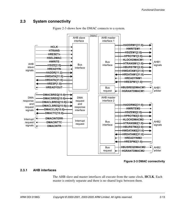
Figure 2-3 shows how the DMAC connects to a system.
Figure 2-3 DMAC connectivity
2.3.1 AHB interfaces
The AHB slave and master interfaces all execute from the same clock, HCLK. Each master is entirely separate and there is no shared logic between them.
ARM DDI 0196G Copyright © 2000-2001, 2003-2005 ARM Limited. All rights reserved. 2-13
Functional Overview
2.3.2 AHB slave interface
The AHB slave interface programs the DMAC. Figure 2-3 on page 2-13 shows the port-level connections of the AHB slave interface module.
2.3.3 AHB master interface
Unless otherwise stated, you must connect this interface as the AMBA Specification describes. You can set the AHB signals while performing DMA transfers.
Protection control
Software programs HPROT[3:0] bits for each DMA channel. The bits are set as follows:
HPROT[0] Opcode, or data. This bit is hardcoded to Data-1.
HPROT[1] User or privileged:
user = 0
privileged = 1.
Programmed by software. See Channel Control Registers on page 3-23. During LLI loads, HPROT[1] is made 1, privileged.
HPROT[2] Bufferable or non-bufferable:
non-bufferable = 0
bufferable = 1.
Programmed by software. See Channel Control Registers on page 3-23. During LLI loads, HPROT[2] is made 0.
HPROT[3] Cacheable or non-cacheable:
non-cacheable = 0
cacheable = 1.
Programmed by software. See Channel Control Registers on page 3-23. During LLI loads, HPROT[3] is made 1.
2-14 Copyright © 2000-2001, 2003-2005 ARM Limited. All rights reserved. ARM DDI 0196G
Functional Overview
Peripherals can interpret the HPROT information as required to help perform efficient transactions. For example:
• You can use the HPROT[1] user or privileged bit to protect certain peripherals or memory spaces from user mode transactions.
• You can use the HPROT[2] bufferable or nonbufferable bit to indicate to an AMBA bridge that the write can complete in zero wait states on the source bus. This is without waiting for it to arbitrate for the destination bus, and for the slave to accept the data.
• An AMBA bridge can use the HPROT[3] cacheable or noncacheable bit so that on the first read of a burst of eight, it can transfer the whole burst of eight reads on the destination bus, rather than pass the transactions through one at a time.
Lock control
Set the lock bit by programming bit 16 in the DMACCxConfiguration Register. See Channel Configuration Registers on page 3-27.
When a burst occurs, the AHB arbiter must not degrant the master during the burst until the lock is deasserted. You can lock the DMAC for a single burst such as a long source fetch burst or a long destination drain burst. The DMAC does not usually assert the lock continuously for a source fetch burst followed by a destination drain burst.
There are situations when the DMAC asserts the lock for source transfers followed by destination transfers. This is possible when internal conditions in the DMAC enable it to perform a source fetch followed by a destination drain back-to-back, and when the following conditions are both met:
• Source width = destination width, and,
• Source burst size is a minimum of 4.
Bus width
The source width, SWidth, or destination width, DWidth, values in the DMACCxControl Register program the HSIZE[1:0] bits.
ARM DDI 0196G Copyright © 2000-2001, 2003-2005 ARM Limited. All rights reserved. 2-15
Functional Overview
2.3.4 Interrupt generation logic
The DMAC generates the individual maskable active HIGH interrupts. A combined interrupt output is also generated as an OR function of the individual interrupt requests.
You can use the single combined interrupt with a system interrupt controller that provides another level of masking on a per-peripheral basis. This enables you to use modular device drivers that always know where to find the interrupt source control register bits.
You can also use the individual interrupt requests with a system interrupt controller that provides masking for the outputs of each peripheral. In this way, a global interrupt service routine can read the entire set of sources from one wide register in the system interrupt controller. This is useful when the time to read from the peripheral registers is significant compared to the CPU clock speed in a real-time system.
The peripheral supports both of these methods.
2.3.5 Interrupt controller connectivity
You can connect the interrupt request signals of the DMAC to an interrupt controller in one of two ways.
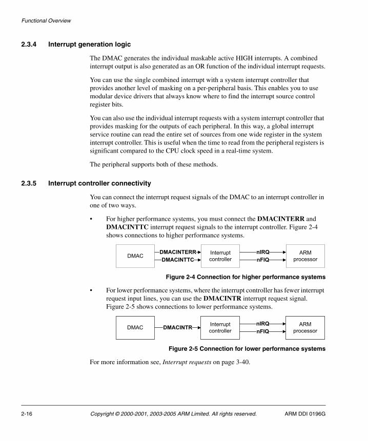
• For higher performance systems, you must connect the DMACINTERR and DMACINTTC interrupt request signals to the interrupt controller. Figure 2-4 shows connections to higher performance systems.
Figure 2-4 Connection for higher performance systems
• For lower performance systems, where the interrupt controller has fewer interrupt request input lines, you can use the DMACINTR interrupt request signal. Figure 2-5 shows connections to lower performance systems.
Figure 2-5 Connection for lower performance systems
For more information see, Interrupt requests on page 3-40.
2-16 Copyright © 2000-2001, 2003-2005 ARM Limited. All rights reserved. ARM DDI 0196G
Functional Overview
2.3.6 DMA request and response connectivity
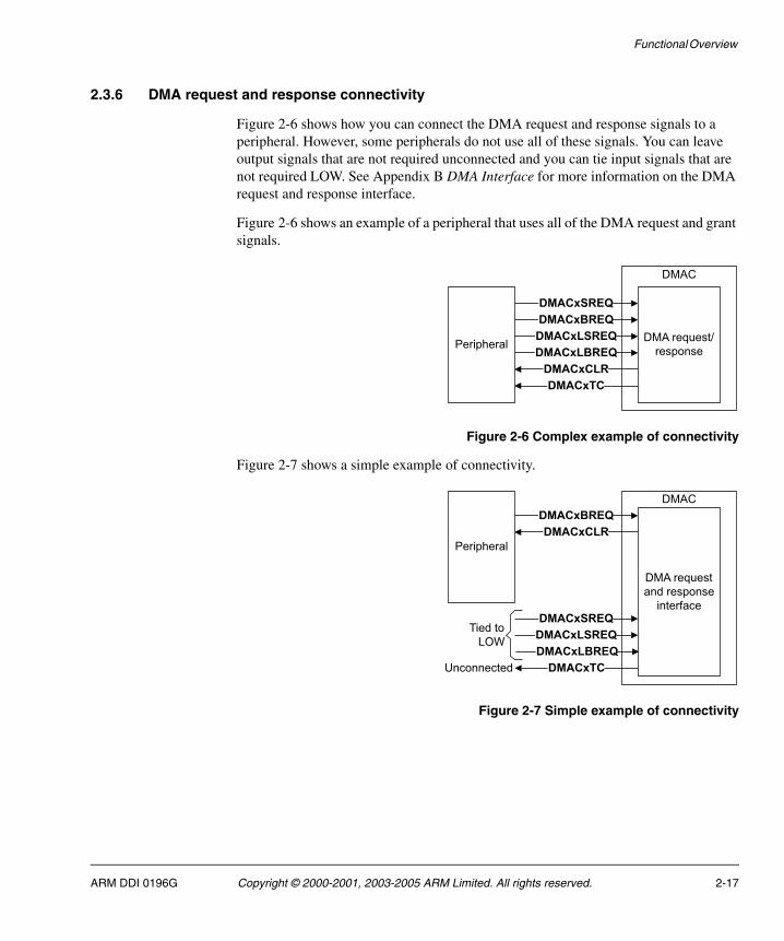
Figure 2-6 shows how you can connect the DMA request and response signals to a peripheral. However, some peripherals do not use all of these signals. You can leave output signals that are not required unconnected and you can tie input signals that are not required LOW. See Appendix B DMA Interface for more information on the DMA request and response interface.
Figure 2-6 shows an example of a peripheral that uses all of the DMA request and grant signals.
Figure 2-6 Complex example of connectivity
Figure 2-7 shows a simple example of connectivity.
Figure 2-7 Simple example of connectivity
ARM DDI 0196G Copyright © 2000-2001, 2003-2005 ARM Limited. All rights reserved. 2-17
Functional Overview
2.4 Software considerations
You must take into account the following software considerations when programming the DMAC:
• There must not be any write-operation to Channel registers in an active channel after the channel enable is made HIGH. If you must reprogram any DMAC channel parameters, you must reprogram after disabling the DMAC channel.
• If the source width is less than the destination width, the TransferSize value multiplied by the source width must be an integral multiple of the destination width.
• When the source peripheral is the flow controller and the source width is less than the destination width, the number of transfers that the source peripheral performs, before asserting an DMACLSREQ or DMACLBREQ, must be so that the number of transfers multiplied by the source width is an integral multiple of the destination width. If this case is violated, the data can get stuck and lost in the FIFO causing UNPREDICTABLE results. You can abort the transfer by disabling the relevant DMAC channel.
• You must not program the SrcPeripheral and DestPeripheral bit fields in the DMACCxConfig Register with any value greater than 15. See Channel Configuration Registers on page 3-27.
• The SWidth and DWidth bit fields in the DMACCxControl Register must not indicate more than a 32-bit wide peripheral. See Channel Control Registers on page 3-23.
• After the software disables a channel by clearing the ChannelEnable bit in the DMACCxConfig Register, see Channel Configuration Registers on page 3-27, it must re-enable the bit only after it has polled a 0 in the corresponding DMACEnbldChns Register bit, see Enabled Channel Register on page 3-14. This is because the actual disabling does not immediately happen with the clearing of ChannelEnable bit. You must accommodate the latency of the ongoing AHB burst.
• The LLI field in the DMACCxLLIReg Register must not indicate an address greater than 0xFFFFFFF0, otherwise the four-word LLI burst wraps over at 0x00000000 and the LLI data structure is not in contiguous memory locations. See Channel Linked List Item Registers on page 3-22.
• When the transfer size programmed in the DMAC is greater than the depth of the FIFO in a source or destination peripheral, you must only program the DMAC for non-incrementing address generation.
2-18 Copyright © 2000-2001, 2003-2005 ARM Limited. All rights reserved. ARM DDI 0196G
Functional Overview
• A peripheral is expected to deassert any DMACSREQ, DMACBREQ, DMACLSREQ, or DMACLBREQ signals on receiving the DMACCLR signal irrespective of the request the DMACCLR was asserted in response to. This is because DMACCLR is not specific to a single-request signal, DMACSREQ, or burst-request signal, DMACSBEQ. The handshaking of DMACCLR is achieved with a logical OR of all the DMA requests in the DMAC.
Note It is illegal for a peripheral to give a new DMACSREQ or DMACBREQ signal
while DMACCLR is HIGH.
• If you program the TransferSize field in the DMACCxControl Register, see Channel Control Registers on page 3-23, as zero, and the DMAC is the flow controller, the TransferSize field has no meaning in other flow-control modes, then the channel does not initiate any transfers. It is your responsibility to disable the channel by writing into the channel enable bit of the DMACCxConfig Register and reprogramming the channel again.
• You must not run the normal read-write tests on the DMACCxControl Register, see Channel Control Registers on page 3-23, because the TransferSize field is not a typical write and read-back register field. While writing, the TransferSize bit-field is like a control register because it determines how many transfers the DMAC performs. However, during read-back, TransferSize behaves like a status register because it returns the number of remaining transfers in terms of source width. So when TransferSize is read back, it returns the number of destination-transfer-completed stored in a separate counter called TrfSizeDst multiplied by a factor. The same physical register is not being written into and read from, and normal write and read-back tests are not applicable.
• In the destination flow control mode, with peripheral-to-peripheral transfer, if sufficient data is present in the channel FIFO to service a DMACLSREQ or DMACLBREQ request raised by a destination peripheral without requiring data to be fetched from the source peripheral, then the source peripheral is issued a DMACTC.
• For destination flow controlled case, peripheral-to-peripheral transfer, with DWidth < SWidth, the number of data bytes requested by the destination peripheral must be an integral multiple of Swidth expressed in bytes. If you do not ensure this, then the DMAC might fetch more data from the source peripheral than is required. This can result in data loss.
ARM DDI 0196G Copyright © 2000-2001, 2003-2005 ARM Limited. All rights reserved. 2-19
Functional Overview
• At the end of accesses corresponding to low-priority channels, an IDLE cycle is inserted on the AHB bus to enable other masters to access the bus. This ensures that a low-priority channel does not monopolize the bus. It does, however, mean that the bus might be occupied by transactions corresponding to a low priority for up to 16 cycles in the worst case. This applies to all transfer configurations, including memory-to-memory transfers.
2-20 Copyright © 2000-2001, 2003-2005 ARM Limited. All rights reserved. ARM DDI 0196G
Functional Overview
2.5 Use with memory management unit based systems
When using the DMAC with a Memory Management Unit (MMU) based system, application code running on the ARM core in virtual memory creates and manages the scatter/gather linked list and the DMAC in physical memory reads it.
Ensure that the area of memory you use for the linked list is flat-mapped. This means that the virtual addresses and physical addresses are the same.
ARM DDI 0196G Copyright © 2000-2001, 2003-2005 ARM Limited. All rights reserved. 2-21
Functional Overview
2-22 Copyright © 2000-2001, 2003-2005 ARM Limited. All rights reserved. ARM DDI 0196G
Chapter 3 Programmer’s Model
This chapter describes the DMAC registers and provides details required when programming the microcontroller. It contains the following sections:
• About the programmer’s model on page 3-2
• Programming the DMAC on page 3-3
• Summary of registers on page 3-6
• Register descriptions on page 3-10
• Address generation on page 3-37
• Scatter/gather on page 3-38
• Interrupt requests on page 3-40
• DMAC data flow on page 3-43.
ARM DDI 0196G Copyright © 2000-2001, 2003-2005 ARM Limited. All rights reserved. 3-1
Programmer’s Model
3.1 About the programmer’s model
The DMAC enables the following types of transactions:
• memory-to-memory
• memory-to-peripheral
• peripheral-to-memory
• peripheral-to-peripheral.
Each DMA stream is configured to provide unidirectional DMA transfers for a single source and destination.
For example, a bidirectional serial port requires one stream for transmit and one for receive. The source and destination areas can each be either a memory region or a peripheral, and you can access them through the same AHB master, or one area by each master.
The base address of the DMAC is not fixed, and can be different for any particular system implementation. However, the offset of any particular register from the base address is fixed.
3.1.1 Register fields
The following applies to the registers that the DMAC uses:
• You must not access reserved or unused address locations because this can result in unpredictable behavior of the device.
• You must write reserved or unused bits of registers as zero, and ignore them on read unless otherwise stated in the relevant text.
• A system or power-on reset resets all register bits to a logic 0 unless otherwise stated in the relevant text.
• All registers support read and write accesses unless otherwise stated in the relevant text. A write updates the contents of a register, and a read returns the contents of the register.
• You can only access registers defined in this document using word reads and word writes, unless otherwise stated in the relevant text.
3-2 Copyright © 2000-2001, 2003-2005 ARM Limited. All rights reserved. ARM DDI 0196G
Programmer’s Model
3.2 Programming the DMAC
All transactions on the AHB slave programming bus must be 32 bits wide. This eliminates endian issues when programming the DMAC. This section provides more information on programming the DMAC:
• Enabling the DMAC
• Disabling the DMAC
• Enabling a DMA channel
• Disabling a DMA channel on page 3-4
• Setting up a new DMA transfer on page 3-5
• Halting a DMA channel on page 3-5
• Programming a DMA channel on page 3-5.
3.2.1 Enabling the DMAC
Enable the DMAC by setting the DMA Enable, E, bit in the DMACConfiguration Register. See Configuration Register on page 3-18.
3.2.2 Disabling the DMAC
To disable the DMAC:
1. Read the DMACEnbldChns Register and ensure that you have disabled all the DMA channels. If any channels are active, see Disabling a DMA channel on page 3-4.
2. Disable the DMAC by writing 0 to the DMA Enable bit in the DMACConfiguration Register. See Configuration Register on page 3-18.
3.2.3 Enabling a DMA channel
Enable the DMA channel by setting the Channel Enable bit in the relevant DMA channel Configuration Register. See Channel Configuration Registers on page 3-27.
Note You must fully initialize the channel before you enable it. Additionally, you must set the Enable bit of the DMAC before you enable any channels.
ARM DDI 0196G Copyright © 2000-2001, 2003-2005 ARM Limited. All rights reserved. 3-3
Programmer’s Model
3.2.4 Disabling a DMA channel
You can disable a DMA channel in the following ways:
• Write directly to the Channel Enable bit.
Note You lose any outstanding data in the FIFOs if you use this method.
• Use the Active and Halt bits in conjunction with the Channel Enable bit.
• Wait until the transfer completes. The channel is then automatically disabled.
Disabling a DMA channel and losing data in the FIFO
Clear the relevant Channel Enable bit in the relevant channel Configuration Register. See Channel Configuration Registers on page 3-27. The current AHB transfer, if one is in progress, completes and the channel is disabled.
Note You lose any data in the FIFO.
Disabling a DMA channel without losing data in the FIFO
To disable a DMA channel without losing data in the FIFO:
1. Set the Halt bit in the relevant channel Configuration Register. See Channel Configuration Registers on page 3-27. This causes any subsequent DMA requests to be ignored.
2. Poll the Active bit in the relevant channel Configuration Register until it reaches 0. This bit indicates whether there is any data in the channel that has to be transferred.
3. Clear the Channel Enable bit in the relevant channel Configuration Register.
3-4 Copyright © 2000-2001, 2003-2005 ARM Limited. All rights reserved. ARM DDI 0196G
Programmer’s Model
3.2.5 Setting up a new DMA transfer
To set up a new DMA transfer:
1. If the channel is not set aside for the DMA transaction:
a. Read the DMACEnbldChns Register and determine the channels that are inactive. See Enabled Channel Register on page 3-14.
b. Choose an inactive channel that has the necessary priority.
2. Program the DMAC.
3.2.6 Halting a DMA channel
Set the Halt bit in the relevant DMA channel Configuration Register. The current source request is serviced. Any subsequent source DMA requests are ignored until the Halt bit is cleared.
3.2.7 Programming a DMA channel
To program a DMA channel:
1. Choose a free DMA channel with the necessary priority. DMA channel 0 has the highest priority and DMA channel 7 has the lowest priority.
2. Clear any pending interrupts on the channel you want to use by writing to the DMACIntTCClear and DMACIntErrClr Registers. See Interrupt Terminal Count Clear Register on page 3-11 and Interrupt Error Clear Register on page 3-12. The previous channel operation might have left interrupts active.
3. Write the source address into the DMACCxSrcAddr Register. See Channel Source Address Registers on page 3-21.
4. Write the destination address into the DMACCxDestAddr Register. See Channel Destination Address Registers on page 3-21.
5. Write the address of the next LLI into the DMACCxLLI Register. See Channel Linked List Item Registers on page 3-22. If the transfer consists of a single packet of data, you must write 0 into this register.
6. Write the control information into the DMACCxControl Register. See Channel Control Registers on page 3-23.
7. Write the channel configuration information into the DMACCxConfiguration Register. See Channel Configuration Registers on page 3-27. If the Enable bit is set, then the DMA channel is automatically enabled.
ARM DDI 0196G Copyright © 2000-2001, 2003-2005 ARM Limited. All rights reserved. 3-5
Programmer’s Model
3.3 Summary of registers
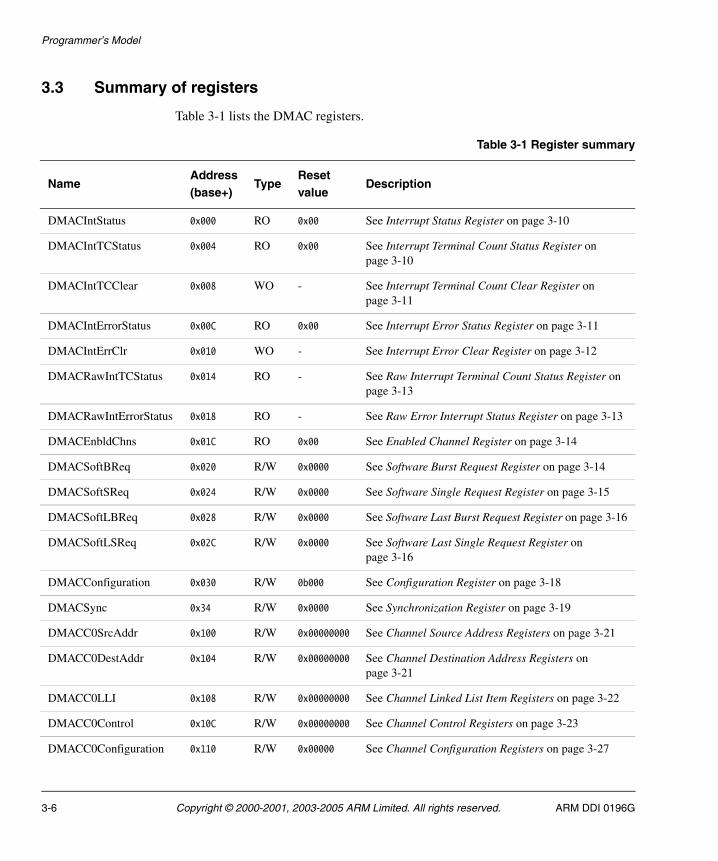
Table 3-1 lists the DMAC registers.
Table 3-1 Register summary
NameAddress(base+)
TypeResetvalue
Description
DMACIntStatus 0x000 RO 0x00 See Interrupt Status Register on page 3-10
DMACIntTCStatus 0x004 RO 0x00 See Interrupt Terminal Count Status Register on page 3-10
DMACIntTCClear 0x008 WO - See Interrupt Terminal Count Clear Register on page 3-11
DMACIntErrorStatus 0x00C RO 0x00 See Interrupt Error Status Register on page 3-11
DMACIntErrClr 0x010 WO - See Interrupt Error Clear Register on page 3-12
DMACRawIntTCStatus 0x014 RO - See Raw Interrupt Terminal Count Status Register on page 3-13
DMACRawIntErrorStatus 0x018 RO - See Raw Error Interrupt Status Register on page 3-13
DMACEnbldChns 0x01C RO 0x00 See Enabled Channel Register on page 3-14
DMACSoftBReq 0x020 R/W 0x0000 See Software Burst Request Register on page 3-14
DMACSoftSReq 0x024 R/W 0x0000 See Software Single Request Register on page 3-15
DMACSoftLBReq 0x028 R/W 0x0000 See Software Last Burst Request Register on page 3-16
DMACSoftLSReq 0x02C R/W 0x0000 See Software Last Single Request Register on page 3-16
DMACConfiguration 0x030 R/W 0b000 See Configuration Register on page 3-18
DMACSync 0x34 R/W 0x0000 See Synchronization Register on page 3-19
DMACC0SrcAddr 0x100 R/W 0x00000000 See Channel Source Address Registers on page 3-21
DMACC0DestAddr 0x104 R/W 0x00000000 See Channel Destination Address Registers on page 3-21
DMACC0LLI 0x108 R/W 0x00000000 See Channel Linked List Item Registers on page 3-22
DMACC0Control 0x10C R/W 0x00000000 See Channel Control Registers on page 3-23
DMACC0Configuration 0x110 R/W 0x00000 See Channel Configuration Registers on page 3-27
3-6 Copyright © 2000-2001, 2003-2005 ARM Limited. All rights reserved. ARM DDI 0196G
Programmer’s Model
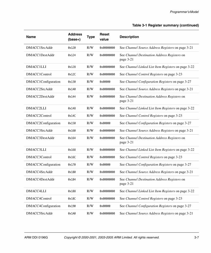
DMACC1SrcAddr 0x120 R/W 0x00000000 See Channel Source Address Registers on page 3-21
DMACC1DestAddr 0x124 R/W 0x00000000 See Channel Destination Address Registers on page 3-21
DMACC1LLI 0x128 R/W 0x00000000 See Channel Linked List Item Registers on page 3-22
DMACC1Control 0x12C R/W 0x00000000 See Channel Control Registers on page 3-23
DMACC1Configuration 0x130 R/W 0x00000 See Channel Configuration Registers on page 3-27
DMACC2SrcAddr 0x140 R/W 0x00000000 See Channel Source Address Registers on page 3-21
DMACC2DestAddr 0x144 R/W 0x00000000 See Channel Destination Address Registers on page 3-21
DMACC2LLI 0x148 R/W 0x00000000 See Channel Linked List Item Registers on page 3-22
DMACC2Control 0x14C R/W 0x00000000 See Channel Control Registers on page 3-23
DMACC2Configuration 0x150 R/W 0x00000 See Channel Configuration Registers on page 3-27
DMACC3SrcAddr 0x160 R/W 0x00000000 See Channel Source Address Registers on page 3-21
DMACC3DestAddr 0x164 R/W 0x00000000 See Channel Destination Address Registers on page 3-21
DMACC3LLI 0x168 R/W 0x00000000 See Channel Linked List Item Registers on page 3-22
DMACC3Control 0x16C R/W 0x00000000 See Channel Control Registers on page 3-23
DMACC3Configuration 0x170 R/W 0x00000 See Channel Configuration Registers on page 3-27
DMACC4SrcAddr 0x180 R/W 0x00000000 See Channel Source Address Registers on page 3-21
DMACC4DestAddr 0x184 R/W 0x00000000 See Channel Destination Address Registers on page 3-21
DMACC4LLI 0x188 R/W 0x00000000 See Channel Linked List Item Registers on page 3-22
DMACC4Control 0x18C R/W 0x00000000 See Channel Control Registers on page 3-23
DMACC4Configuration 0x190 R/W 0x00000 See Channel Configuration Registers on page 3-27
DMACC5SrcAddr 0x1A0 R/W 0x00000000 See Channel Source Address Registers on page 3-21
Table 3-1 Register summary (continued)
NameAddress(base+)
TypeResetvalue
Description
ARM DDI 0196G Copyright © 2000-2001, 2003-2005 ARM Limited. All rights reserved. 3-7
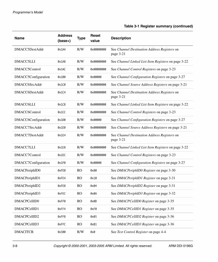
Programmer’s Model
DMACC5DestAddr 0x1A4 R/W 0x00000000 See Channel Destination Address Registers on page 3-21
DMACC5LLI 0x1A8 R/W 0x00000000 See Channel Linked List Item Registers on page 3-22
DMACC5Control 0x1AC R/W 0x00000000 See Channel Control Registers on page 3-23
DMACC5Configuration 0x1B0 R/W 0x00000 See Channel Configuration Registers on page 3-27
DMACC6SrcAddr 0x1C0 R/W 0x00000000 See Channel Source Address Registers on page 3-21
DMACC6DestAddr 0x1C4 R/W 0x00000000 See Channel Destination Address Registers on page 3-21
DMACC6LLI 0x1C8 R/W 0x00000000 See Channel Linked List Item Registers on page 3-22
DMACC6Control 0x1CC R/W 0x00000000 See Channel Control Registers on page 3-23
DMACC6Configuration 0x1D0 R/W 0x00000 See Channel Configuration Registers on page 3-27
DMACC7SrcAddr 0x1E0 R/W 0x00000000 See Channel Source Address Registers on page 3-21
DMACC7DestAddr 0x1E4 R/W 0x00000000 See Channel Destination Address Registers on page 3-21
DMACC7LLI 0x1E8 R/W 0x00000000 See Channel Linked List Item Registers on page 3-22
DMACC7Control 0x1EC R/W 0x00000000 See Channel Control Registers on page 3-23
DMACC7Configuration 0x1F0 R/W 0x00000 See Channel Configuration Registers on page 3-27
DMACPeriphID0 0xFE0 RO 0x80 See DMACPeriphID0 Register on page 3-30
DMACPeriphID1 0xFE4 RO 0x10 See DMACPeriphID1 Register on page 3-31
DMACPeriphID2 0xFE8 RO 0x04 See DMACPeriphID2 Register on page 3-31
DMACPeriphID3 0xFEC RO 0x0A See DMACPeriphID3 Register on page 3-32
DMACPCellID0 0xFF0 RO 0x0D See DMACPCellID0 Register on page 3-35
DMACPCellID1 0xFF4 RO 0xF0 See DMACPCellID1 Register on page 3-35
DMACPCellID2 0xFF8 RO 0x05 See DMACPCellID2 Register on page 3-36
DMACPCellID3 0xFFC RO 0xB1 See DMACPCellID3 Register on page 3-36
DMACITCR 0x500 R/W 0x0 See Test Control Register on page 4-4
Table 3-1 Register summary (continued)
NameAddress(base+)
TypeResetvalue
Description
3-8 Copyright © 2000-2001, 2003-2005 ARM Limited. All rights reserved. ARM DDI 0196G
Programmer’s Model
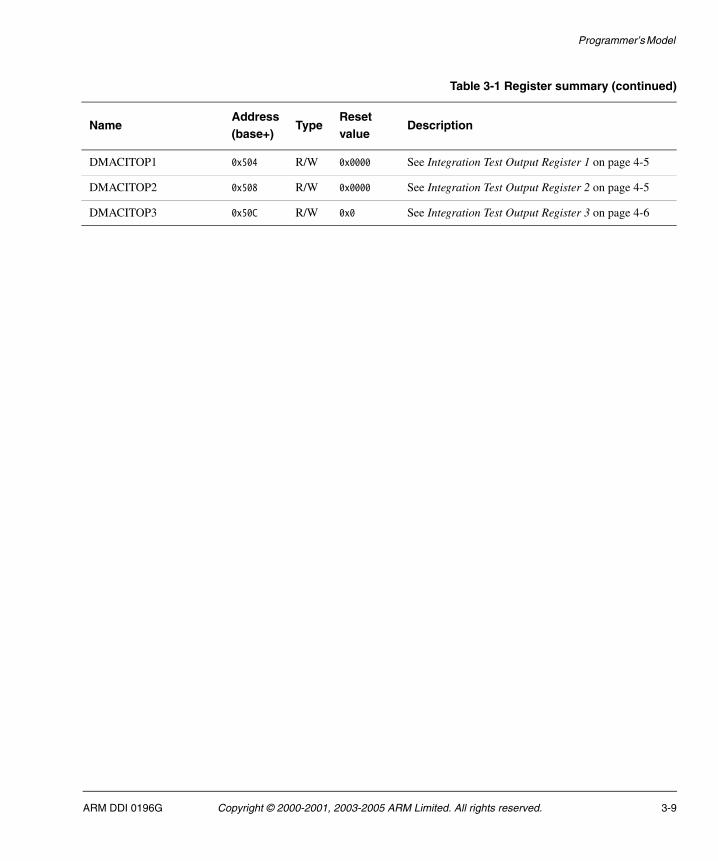
DMACITOP1 0x504 R/W 0x0000 See Integration Test Output Register 1 on page 4-5
DMACITOP2 0x508 R/W 0x0000 See Integration Test Output Register 2 on page 4-5
DMACITOP3 0x50C R/W 0x0 See Integration Test Output Register 3 on page 4-6
Table 3-1 Register summary (continued)
NameAddress(base+)
TypeResetvalue
Description
ARM DDI 0196G Copyright © 2000-2001, 2003-2005 ARM Limited. All rights reserved. 3-9
Programmer’s Model
3.4 Register descriptions
This section describes the DMAC registers. Table 3-1 on page 3-6 provides cross references to the relevant sections.
3.4.1 Interrupt Status Register
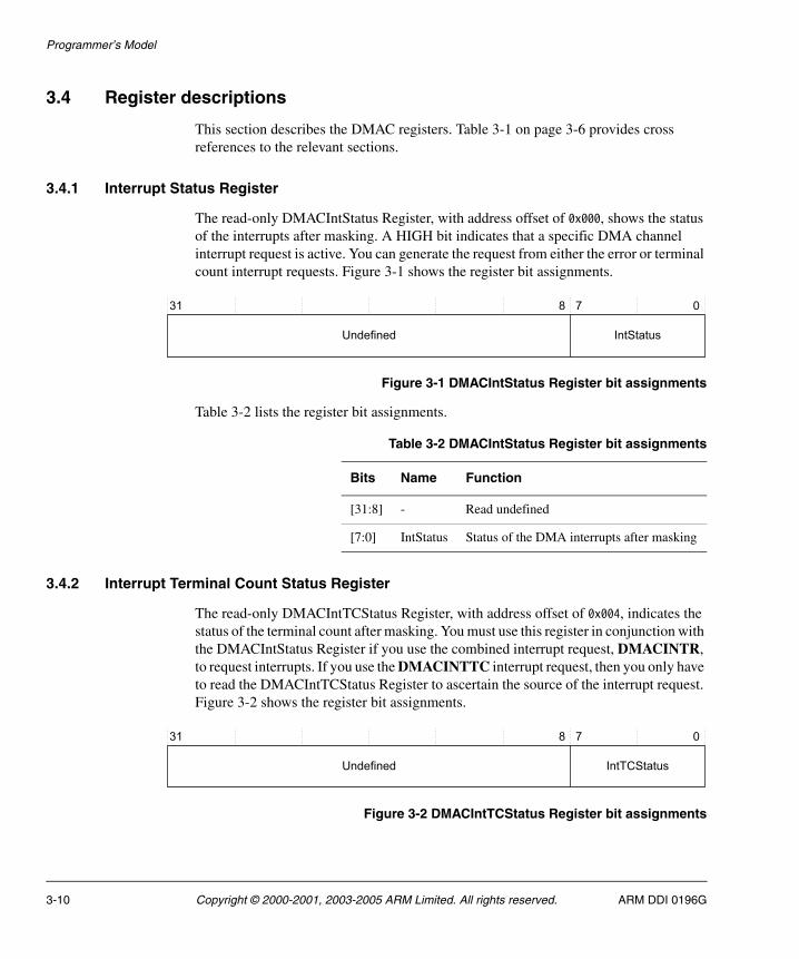
The read-only DMACIntStatus Register, with address offset of 0x000, shows the status of the interrupts after masking. A HIGH bit indicates that a specific DMA channel interrupt request is active. You can generate the request from either the error or terminal count interrupt requests. Figure 3-1 shows the register bit assignments.
Figure 3-1 DMACIntStatus Register bit assignments
Table 3-2 lists the register bit assignments.
3.4.2 Interrupt Terminal Count Status Register
The read-only DMACIntTCStatus Register, with address offset of 0x004, indicates the status of the terminal count after masking. You must use this register in conjunction with the DMACIntStatus Register if you use the combined interrupt request, DMACINTR, to request interrupts. If you use the DMACINTTC interrupt request, then you only have to read the DMACIntTCStatus Register to ascertain the source of the interrupt request. Figure 3-2 shows the register bit assignments.
Figure 3-2 DMACIntTCStatus Register bit assignments
Table 3-2 DMACIntStatus Register bit assignments
Bits Name Function
[31:8] - Read undefined
[7:0] IntStatus Status of the DMA interrupts after masking
3-10 Copyright © 2000-2001, 2003-2005 ARM Limited. All rights reserved. ARM DDI 0196G
Programmer’s Model
Table 3-3 lists the register bit assignments.
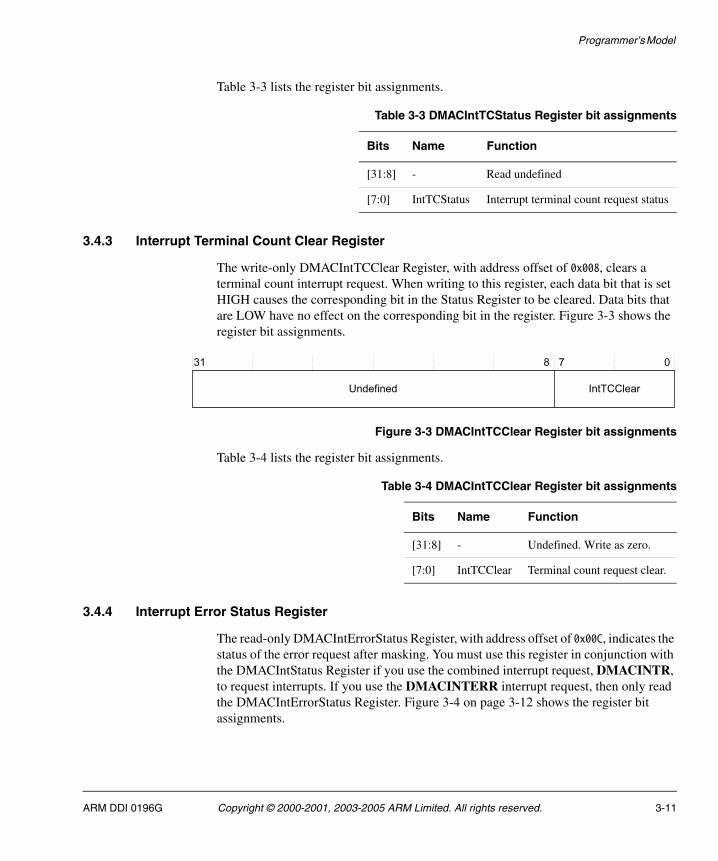
3.4.3 Interrupt Terminal Count Clear Register
The write-only DMACIntTCClear Register, with address offset of 0x008, clears a terminal count interrupt request. When writing to this register, each data bit that is set HIGH causes the corresponding bit in the Status Register to be cleared. Data bits that are LOW have no effect on the corresponding bit in the register. Figure 3-3 shows the register bit assignments.
Figure 3-3 DMACIntTCClear Register bit assignments
Table 3-4 lists the register bit assignments.
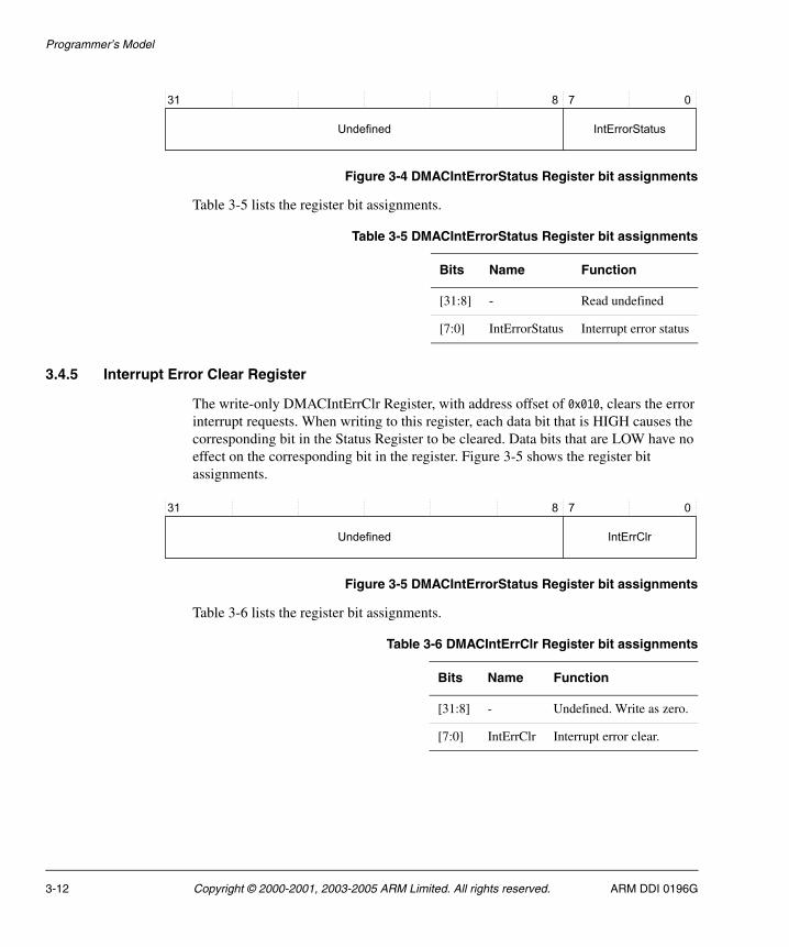
3.4.4 Interrupt Error Status Register
The read-only DMACIntErrorStatus Register, with address offset of 0x00C, indicates the status of the error request after masking. You must use this register in conjunction with the DMACIntStatus Register if you use the combined interrupt request, DMACINTR, to request interrupts. If you use the DMACINTERR interrupt request, then only read the DMACIntErrorStatus Register. Figure 3-4 on page 3-12 shows the register bit assignments.
Table 3-3 DMACIntTCStatus Register bit assignments
Bits Name Function
[31:8] - Read undefined
[7:0] IntTCStatus Interrupt terminal count request status
Table 3-4 DMACIntTCClear Register bit assignments
Bits Name Function
[31:8] - Undefined. Write as zero.
[7:0] IntTCClear Terminal count request clear.
ARM DDI 0196G Copyright © 2000-2001, 2003-2005 ARM Limited. All rights reserved. 3-11
Programmer’s Model
Figure 3-4 DMACIntErrorStatus Register bit assignments
Table 3-5 lists the register bit assignments.
3.4.5 Interrupt Error Clear Register
The write-only DMACIntErrClr Register, with address offset of 0x010, clears the error interrupt requests. When writing to this register, each data bit that is HIGH causes the corresponding bit in the Status Register to be cleared. Data bits that are LOW have no effect on the corresponding bit in the register. Figure 3-5 shows the register bit assignments.
Figure 3-5 DMACIntErrorStatus Register bit assignments
Table 3-6 lists the register bit assignments.
Table 3-5 DMACIntErrorStatus Register bit assignments
Bits Name Function
[31:8] - Read undefined
[7:0] IntErrorStatus Interrupt error status
Table 3-6 DMACIntErrClr Register bit assignments
Bits Name Function
[31:8] - Undefined. Write as zero.
[7:0] IntErrClr Interrupt error clear.
3-12 Copyright © 2000-2001, 2003-2005 ARM Limited. All rights reserved. ARM DDI 0196G
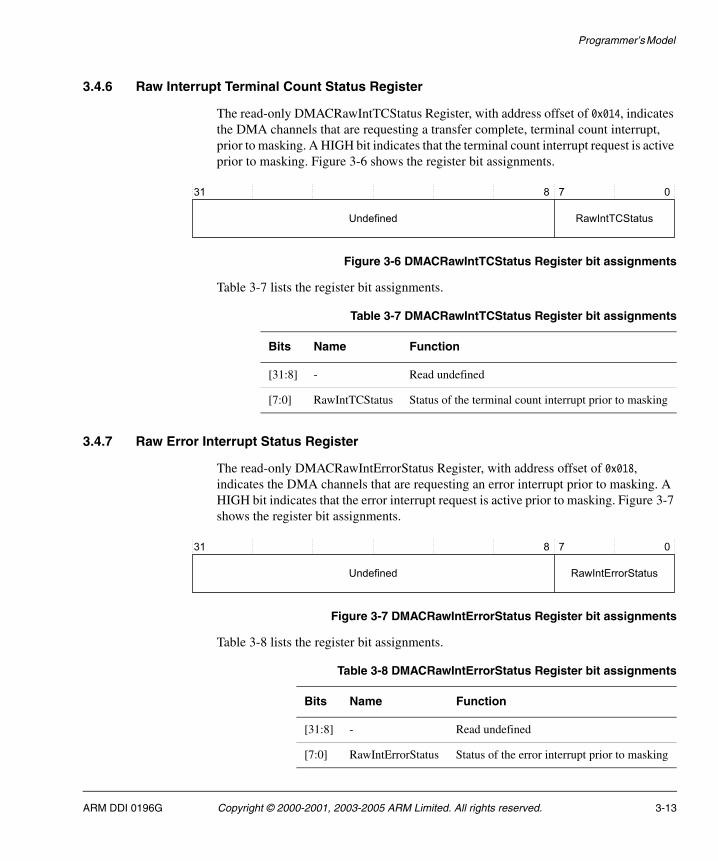
Programmer’s Model
3.4.6 Raw Interrupt Terminal Count Status Register
The read-only DMACRawIntTCStatus Register, with address offset of 0x014, indicates the DMA channels that are requesting a transfer complete, terminal count interrupt, prior to masking. A HIGH bit indicates that the terminal count interrupt request is active prior to masking. Figure 3-6 shows the register bit assignments.
Figure 3-6 DMACRawIntTCStatus Register bit assignments
Table 3-7 lists the register bit assignments.
3.4.7 Raw Error Interrupt Status Register
The read-only DMACRawIntErrorStatus Register, with address offset of 0x018, indicates the DMA channels that are requesting an error interrupt prior to masking. A HIGH bit indicates that the error interrupt request is active prior to masking. Figure 3-7 shows the register bit assignments.
Figure 3-7 DMACRawIntErrorStatus Register bit assignments
Table 3-8 lists the register bit assignments.
Table 3-7 DMACRawIntTCStatus Register bit assignments
Bits Name Function
[31:8] - Read undefined
[7:0] RawIntTCStatus Status of the terminal count interrupt prior to masking
Table 3-8 DMACRawIntErrorStatus Register bit assignments
Bits Name Function
[31:8] - Read undefined
[7:0] RawIntErrorStatus Status of the error interrupt prior to masking
ARM DDI 0196G Copyright © 2000-2001, 2003-2005 ARM Limited. All rights reserved. 3-13
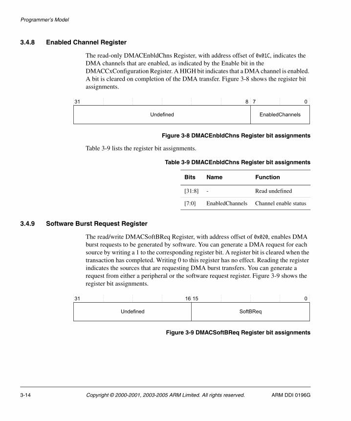
Programmer’s Model
3.4.8 Enabled Channel Register
The read-only DMACEnbldChns Register, with address offset of 0x01C, indicates the DMA channels that are enabled, as indicated by the Enable bit in the DMACCxConfiguration Register. A HIGH bit indicates that a DMA channel is enabled. A bit is cleared on completion of the DMA transfer. Figure 3-8 shows the register bit assignments.
Figure 3-8 DMACEnbldChns Register bit assignments
Table 3-9 lists the register bit assignments.
3.4.9 Software Burst Request Register
The read/write DMACSoftBReq Register, with address offset of 0x020, enables DMA burst requests to be generated by software. You can generate a DMA request for each source by writing a 1 to the corresponding register bit. A register bit is cleared when the transaction has completed. Writing 0 to this register has no effect. Reading the register indicates the sources that are requesting DMA burst transfers. You can generate a request from either a peripheral or the software request register. Figure 3-9 shows the register bit assignments.
Figure 3-9 DMACSoftBReq Register bit assignments
Table 3-9 DMACEnbldChns Register bit assignments
Bits Name Function
[31:8] - Read undefined
[7:0] EnabledChannels Channel enable status
3-14 Copyright © 2000-2001, 2003-2005 ARM Limited. All rights reserved. ARM DDI 0196G
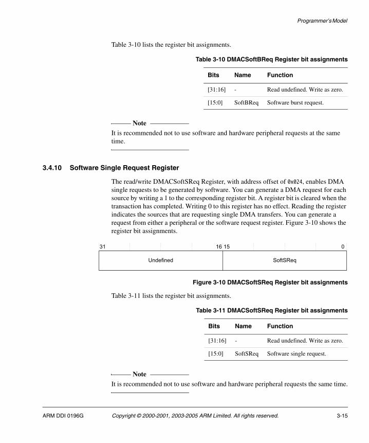
Programmer’s Model
Table 3-10 lists the register bit assignments.
Note It is recommended not to use software and hardware peripheral requests at the same time.
3.4.10 Software Single Request Register
The read/write DMACSoftSReq Register, with address offset of 0x024, enables DMA single requests to be generated by software. You can generate a DMA request for each source by writing a 1 to the corresponding register bit. A register bit is cleared when the transaction has completed. Writing 0 to this register has no effect. Reading the register indicates the sources that are requesting single DMA transfers. You can generate a request from either a peripheral or the software request register. Figure 3-10 shows the register bit assignments.
Figure 3-10 DMACSoftSReq Register bit assignments
Table 3-11 lists the register bit assignments.
Note It is recommended not to use software and hardware peripheral requests the same time.
Table 3-10 DMACSoftBReq Register bit assignments
Bits Name Function
[31:16] - Read undefined. Write as zero.
[15:0] SoftBReq Software burst request.
Table 3-11 DMACSoftSReq Register bit assignments
Bits Name Function
[31:16] - Read undefined. Write as zero.
[15:0] SoftSReq Software single request.
ARM DDI 0196G Copyright © 2000-2001, 2003-2005 ARM Limited. All rights reserved. 3-15
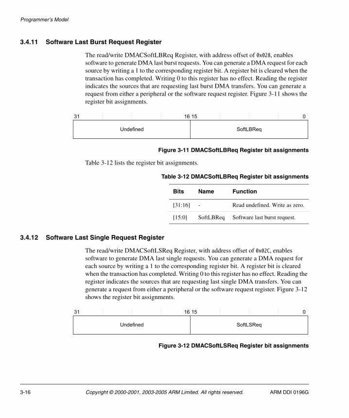
Programmer’s Model
3.4.11 Software Last Burst Request Register
The read/write DMACSoftLBReq Register, with address offset of 0x028, enables software to generate DMA last burst requests. You can generate a DMA request for each source by writing a 1 to the corresponding register bit. A register bit is cleared when the transaction has completed. Writing 0 to this register has no effect. Reading the register indicates the sources that are requesting last burst DMA transfers. You can generate a request from either a peripheral or the software request register. Figure 3-11 shows the register bit assignments.
Figure 3-11 DMACSoftLBReq Register bit assignments
Table 3-12 lists the register bit assignments.
3.4.12 Software Last Single Request Register
The read/write DMACSoftLSReq Register, with address offset of 0x02C, enables software to generate DMA last single requests. You can generate a DMA request for each source by writing a 1 to the corresponding register bit. A register bit is cleared when the transaction has completed. Writing 0 to this register has no effect. Reading the register indicates the sources that are requesting last single DMA transfers. You can generate a request from either a peripheral or the software request register. Figure 3-12 shows the register bit assignments.
Figure 3-12 DMACSoftLSReq Register bit assignments
Table 3-12 DMACSoftLBReq Register bit assignments
Bits Name Function
[31:16] - Read undefined. Write as zero.
[15:0] SoftLBReq Software last burst request.
3-16 Copyright © 2000-2001, 2003-2005 ARM Limited. All rights reserved. ARM DDI 0196G
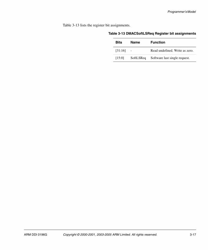
Programmer’s Model
Table 3-13 lists the register bit assignments.
Table 3-13 DMACSoftLSReq Register bit assignments
Bits Name Function
[31:16] - Read undefined. Write as zero.
[15:0] SoftLSReq Software last single request.
ARM DDI 0196G Copyright © 2000-2001, 2003-2005 ARM Limited. All rights reserved. 3-17
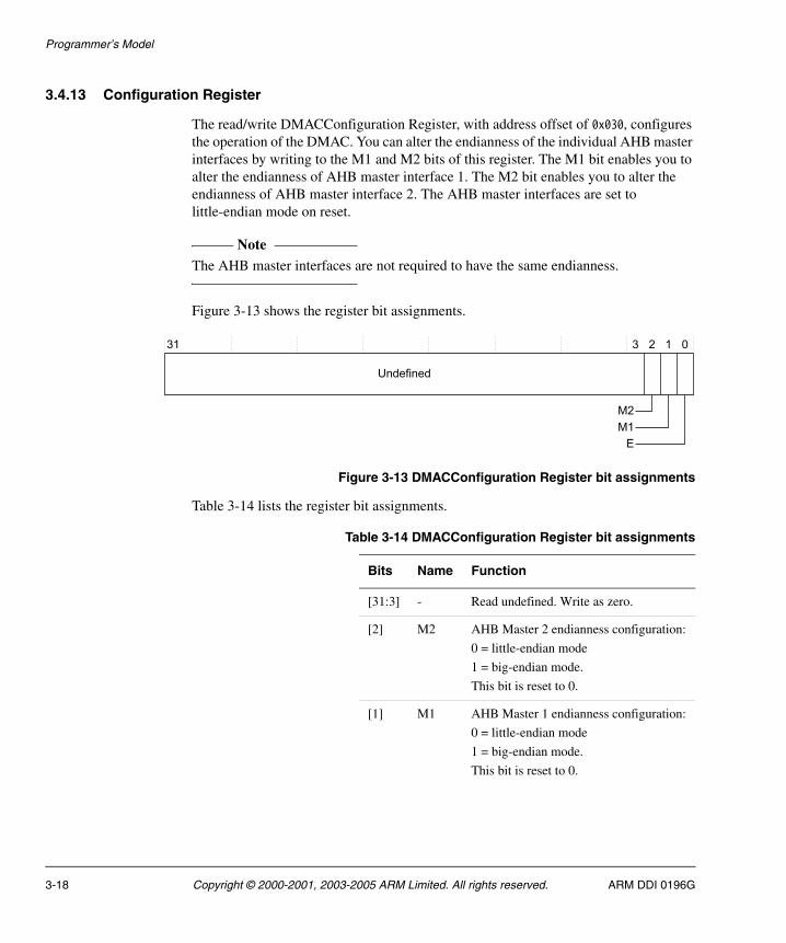
Programmer’s Model
3.4.13 Configuration Register
The read/write DMACConfiguration Register, with address offset of 0x030, configures the operation of the DMAC. You can alter the endianness of the individual AHB master interfaces by writing to the M1 and M2 bits of this register. The M1 bit enables you to alter the endianness of AHB master interface 1. The M2 bit enables you to alter the endianness of AHB master interface 2. The AHB master interfaces are set to little-endian mode on reset.
Note The AHB master interfaces are not required to have the same endianness.
Figure 3-13 shows the register bit assignments.
Figure 3-13 DMACConfiguration Register bit assignments
Table 3-14 lists the register bit assignments.
Table 3-14 DMACConfiguration Register bit assignments
Bits Name Function
[31:3] - Read undefined. Write as zero.
[2] M2 AHB Master 2 endianness configuration:
0 = little-endian mode
1 = big-endian mode.
This bit is reset to 0.
[1] M1 AHB Master 1 endianness configuration:
0 = little-endian mode
1 = big-endian mode.
This bit is reset to 0.
3-18 Copyright © 2000-2001, 2003-2005 ARM Limited. All rights reserved. ARM DDI 0196G
Programmer’s Model
3.4.14 Synchronization Register
The read/write DMACSync Register, with address offset of 0x034, enables or disables synchronization logic for the DMA request signals.
The DMA request signals consist of:
• DMACBREQ[15:0]• DMACSREQ[15:0]• DMACLBREQ[15:0]• DMACLSREQ[15:0].
A bit set to 0 enables the synchronization logic for a particular group of DMA requests. A bit set to 1 disables the synchronization logic for a particular group of DMA requests. This register is reset to 0, and synchronization logic enabled.
Note It is illegal for a peripheral to give a new DMACSREQ or DMACBREQ signal while DMACCLR is HIGH.
Note You must use synchronization logic when the peripheral generating the DMA request runs on a different clock to the DMAC. For peripherals running on the same clock as the DMAC, disabling the synchronization logic improves the DMA request response time. If necessary, synchronize the DMA response signals, DMACCLR and DMACTC, in the peripheral.
Figure 3-14 on page 3-20 shows the register bit assignments.
[0] E DMAC enable:
0 = disabled
1 = enabled.
This bit is reset to 0. Disabling the DMAC reduces power consumption.
Table 3-14 DMACConfiguration Register bit assignments (continued)
Bits Name Function
ARM DDI 0196G Copyright © 2000-2001, 2003-2005 ARM Limited. All rights reserved. 3-19
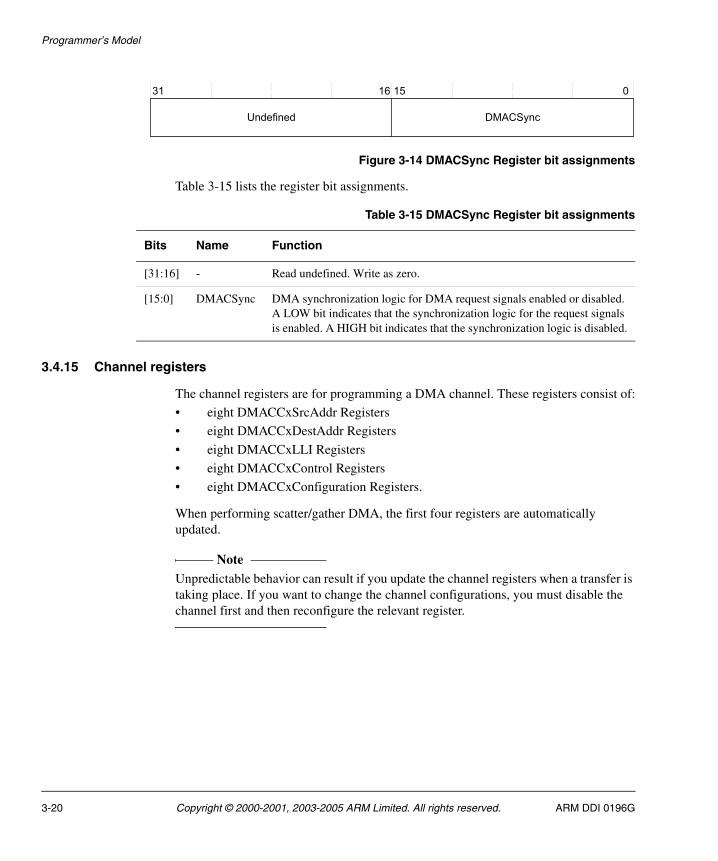
Programmer’s Model
Figure 3-14 DMACSync Register bit assignments
Table 3-15 lists the register bit assignments.
3.4.15 Channel registers
The channel registers are for programming a DMA channel. These registers consist of:
• eight DMACCxSrcAddr Registers
• eight DMACCxDestAddr Registers
• eight DMACCxLLI Registers
• eight DMACCxControl Registers
• eight DMACCxConfiguration Registers.
When performing scatter/gather DMA, the first four registers are automatically updated.
Note Unpredictable behavior can result if you update the channel registers when a transfer is taking place. If you want to change the channel configurations, you must disable the channel first and then reconfigure the relevant register.
Table 3-15 DMACSync Register bit assignments
Bits Name Function
[31:16] - Read undefined. Write as zero.
[15:0] DMACSync DMA synchronization logic for DMA request signals enabled or disabled. A LOW bit indicates that the synchronization logic for the request signals is enabled. A HIGH bit indicates that the synchronization logic is disabled.
3-20 Copyright © 2000-2001, 2003-2005 ARM Limited. All rights reserved. ARM DDI 0196G
Programmer’s Model
Channel Source Address Registers
The eight read/write DMACCxSrcAddr Registers, with address offsets of 0x100, 0x120, 0x140, 0x160, 0x180, 0x1A0, 0x1C0, and 0x1E0 respectively, contain the current source address, byte-aligned, of the data to be transferred. Software programs each register directly before the appropriate channel is enabled.
When the DMA channel is enabled, this register is updated:
• as the source address is incremented
• by following the linked list when a complete packet of data has been transferred.
Reading the register when the channel is active does not provide useful information. This is because by the time the software has processed the value read, the channel might have progressed. It is intended to be read-only when the channel has stopped, and in such case, it shows the source address of the last item read.
Note You must align source and destination addresses to the source and destination widths.
Table 3-16 lists the bit assignments for these registers.
Channel Destination Address Registers
The eight read/write DMACCxDestAddr Registers, with address offsets of 0x104, 0x124, 0x144, 0x164, 0x184, 0x1A4, 0x1C4, and 0x1E4 respectively, contain the current destination address, byte-aligned, of the data to be transferred.
Software programs each register directly before the channel is enabled. When the DMA channel is enabled, the register is updated as the destination address is incremented and by following the linked list when a complete packet of data has been transferred. Reading the register when the channel is active does not provide useful information. This is because by the time the software has processed the value read, the channel might have progressed. It is intended to be read-only when a channel has stopped. In this case, it shows the destination address of the last item read.
Table 3-16 DMACCxSrcAddr Register bit assignments
Bits Name Function
[31:0] SrcAddr DMA source address
ARM DDI 0196G Copyright © 2000-2001, 2003-2005 ARM Limited. All rights reserved. 3-21
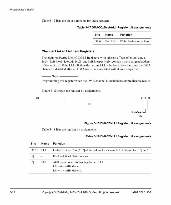
Programmer’s Model
Table 3-17 lists the bit assignments for these registers.
Channel Linked List Item Registers
The eight read/write DMACCxLLI Registers, with address offsets of 0x108, 0x128, 0x148, 0x168, 0x188, 0x1A8, 0x1C8, and 0x1E8 respectively, contain a word-aligned address of the next LLI. If the LLI is 0, then the current LLI is the last in the chain, and the DMA channel is disabled after all DMA transfers associated with it are completed.
Note Programming this register when the DMA channel is enabled has unpredictable results.
Figure 3-15 shows the register bit assignments.
Figure 3-15 DMACCxLLI Register bit assignments
Table 3-18 lists the register bit assignments.
Table 3-17 DMACCxDestAddr Register bit assignments
Bits Name Function
[31:0] DestAddr DMA destination address
Table 3-18 DMACCxLLI Register bit assignments
Bits Name Function
[31:2] LLI Linked list item. Bits [31:2] of the address for the next LLI. Address bits [1:0] are 0.
[1] - Read undefined. Write as zero.
[0] LM AHB master select for loading the next LLI
LM = 0 = AHB Master 1
LM = 1 = AHB Master 2.
3-22 Copyright © 2000-2001, 2003-2005 ARM Limited. All rights reserved. ARM DDI 0196G
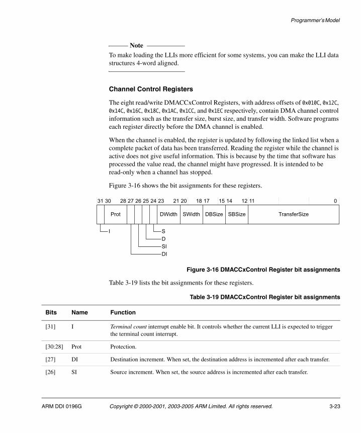
Programmer’s Model
Note To make loading the LLIs more efficient for some systems, you can make the LLI data structures 4-word aligned.
Channel Control Registers
The eight read/write DMACCxControl Registers, with address offsets of 0x010C, 0x12C, 0x14C, 0x16C, 0x18C, 0x1AC, 0x1CC, and 0x1EC respectively, contain DMA channel control information such as the transfer size, burst size, and transfer width. Software programs each register directly before the DMA channel is enabled.
When the channel is enabled, the register is updated by following the linked list when a complete packet of data has been transferred. Reading the register while the channel is active does not give useful information. This is because by the time that software has processed the value read, the channel might have progressed. It is intended to be read-only when a channel has stopped.
Figure 3-16 shows the bit assignments for these registers.
Figure 3-16 DMACCxControl Register bit assignments
Table 3-19 lists the bit assignments for these registers.
Table 3-19 DMACCxControl Register bit assignments
Bits Name Function
[31] I Terminal count interrupt enable bit. It controls whether the current LLI is expected to trigger the terminal count interrupt.
[30:28] Prot Protection.
[27] DI Destination increment. When set, the destination address is incremented after each transfer.
[26] SI Source increment. When set, the source address is incremented after each transfer.
ARM DDI 0196G Copyright © 2000-2001, 2003-2005 ARM Limited. All rights reserved. 3-23
Programmer’s Model
[25] D Destination AHB master select:
0 = AHB master 1 selected for the destination transfer
1 = AHB master 2 selected for the destination transfer.
[24] S Source AHB master select:
0 = AHB master 1 selected for the source transfer
1 = AHB master 2 selected for the source transfer.
[23:21] DWidth Destination transfer width. Transfers wider than the AHB master bus width are illegal. The source and destination widths can be different from each other. The hardware automatically packs and unpacks the data when required.
[20:18] SWidth Source transfer width. Transfers wider than the AHB master bus width are illegal. The source and destination widths can be different from each other. The hardware automatically packs and unpacks the data when required.
[17:15] DBSize Destination burst size. Indicates the number of transfers that make up a destination burst transfer request. You must set this value to the burst size of the destination peripheral, or if the destination is memory, to the memory boundary size. The burst size is the amount of data that is transferred when the DMACxBREQ signal goes active in the destination peripheral. The burst size is not related to the AHB HBURST signal.
[14:12] SBSize Source burst size. Indicates the number of transfers that make up a source burst. You must set this value to the burst size of the source peripheral, or if the source is memory, to the memory boundary size. The burst size is the amount of data that is transferred when the DMACxBREQ signal goes active in the source peripheral. The burst size is not related to the AHB HBURST signal.
[11:0] TransferSize Transfer size. A write to this field sets the size of the transfer when the DMAC is the flow controller.
This value counts down from the original value to zero, and so its value indicates the number of transfers left to complete. A read from this field provides the number of transfers still to be completed on the destination bus. Reading the register when the channel is active does not give useful information because by the time the software has processed the value read, the channel might have progressed. Only use it when a channel is enabled, and then disabled.
The ARM PrimeCell DMA Controller (PL080) Design Manual provides more information about the use of this field.
Program the transfer size value to zero if the DMAC is not the flow controller. If you program the TransferSize to a non-zero value, the DMAC might attempt to use this value instead of ignoring the TransferSize.
Table 3-19 DMACCxControl Register bit assignments (continued)
Bits Name Function
3-24 Copyright © 2000-2001, 2003-2005 ARM Limited. All rights reserved. ARM DDI 0196G
Programmer’s Model
Table 3-20 lists the values of the DBSize or SBSsize bits and their corresponding burst sizes.
Table 3-21 lists the value of the SWidth or DWidth bits and their corresponding widths.
Table 3-20 Source or destination burst size
Bit value of DBSize or SBSize
Source or destination burst transfer request size
0b000 1
0b001 4
0b010 8
0b011 16
0b100 32
0b101 64
0b110 128
0b111 256
Table 3-21 Source or destination transfer width
Bit value of SWidth or DWidth
Source or destination width
0b000 Byte, 8-bit
0b001 Halfword, 16-bit
0b010 Word, 32-bit
0b011 Reserved
0b100 Reserved
0b101 Reserved
0b110 Reserved
0b111 Reserved
ARM DDI 0196G Copyright © 2000-2001, 2003-2005 ARM Limited. All rights reserved. 3-25
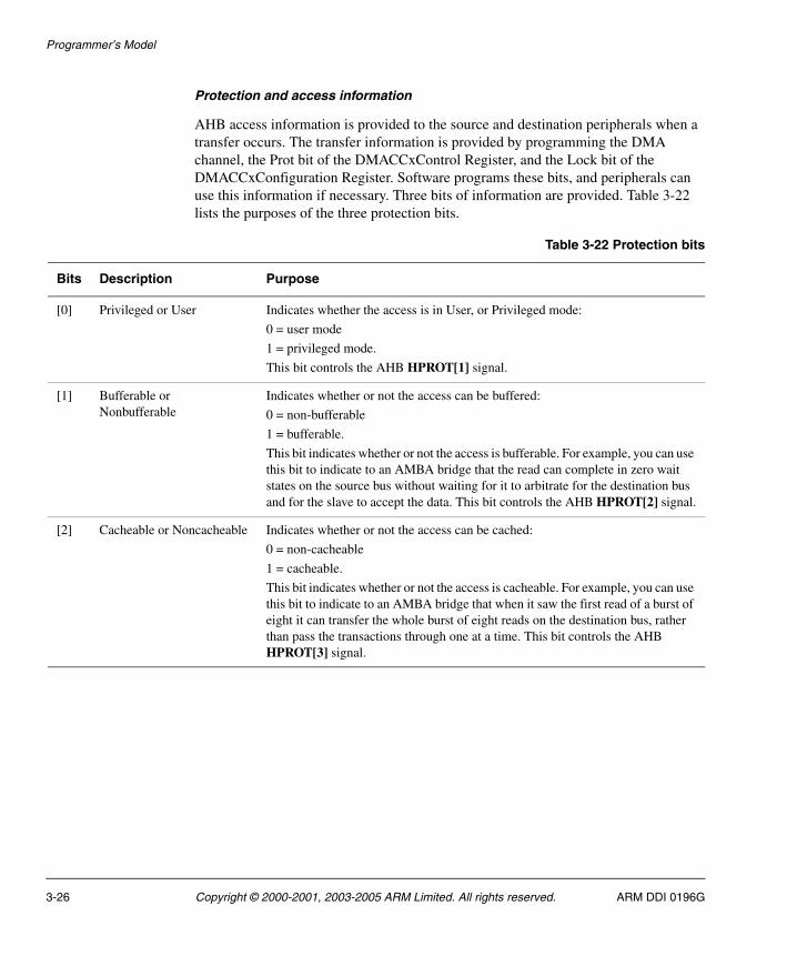
Programmer’s Model
Protection and access information
AHB access information is provided to the source and destination peripherals when a transfer occurs. The transfer information is provided by programming the DMA channel, the Prot bit of the DMACCxControl Register, and the Lock bit of the DMACCxConfiguration Register. Software programs these bits, and peripherals can use this information if necessary. Three bits of information are provided. Table 3-22 lists the purposes of the three protection bits.
Table 3-22 Protection bits
Bits Description Purpose
[0] Privileged or User Indicates whether the access is in User, or Privileged mode:
0 = user mode
1 = privileged mode.
This bit controls the AHB HPROT[1] signal.
[1] Bufferable or Nonbufferable
Indicates whether or not the access can be buffered:
0 = non-bufferable
1 = bufferable.
This bit indicates whether or not the access is bufferable. For example, you can use this bit to indicate to an AMBA bridge that the read can complete in zero wait states on the source bus without waiting for it to arbitrate for the destination bus and for the slave to accept the data. This bit controls the AHB HPROT[2] signal.
[2] Cacheable or Noncacheable Indicates whether or not the access can be cached:
0 = non-cacheable
1 = cacheable.
This bit indicates whether or not the access is cacheable. For example, you can use this bit to indicate to an AMBA bridge that when it saw the first read of a burst of eight it can transfer the whole burst of eight reads on the destination bus, rather than pass the transactions through one at a time. This bit controls the AHB HPROT[3] signal.
3-26 Copyright © 2000-2001, 2003-2005 ARM Limited. All rights reserved. ARM DDI 0196G
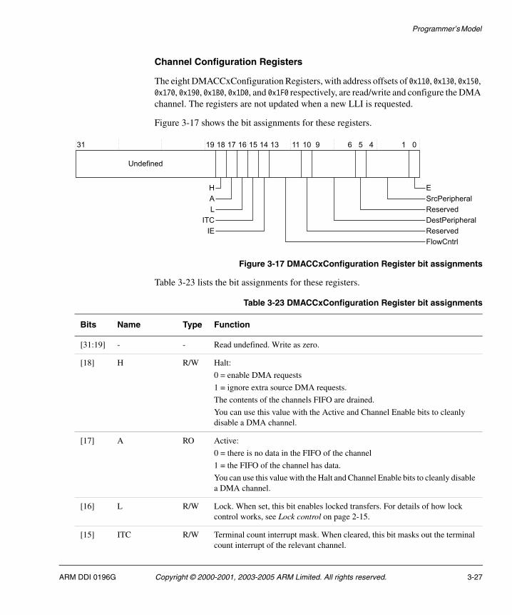
Programmer’s Model
Channel Configuration Registers
The eight DMACCxConfiguration Registers, with address offsets of 0x110, 0x130, 0x150, 0x170, 0x190, 0x1B0, 0x1D0, and 0x1F0 respectively, are read/write and configure the DMA channel. The registers are not updated when a new LLI is requested.
Figure 3-17 shows the bit assignments for these registers.
Figure 3-17 DMACCxConfiguration Register bit assignments
Table 3-23 lists the bit assignments for these registers.
Table 3-23 DMACCxConfiguration Register bit assignments
Bits Name Type Function
[31:19] - - Read undefined. Write as zero.
[18] H R/W Halt:
0 = enable DMA requests
1 = ignore extra source DMA requests.
The contents of the channels FIFO are drained.
You can use this value with the Active and Channel Enable bits to cleanly disable a DMA channel.
[17] A RO Active:
0 = there is no data in the FIFO of the channel
1 = the FIFO of the channel has data.
You can use this value with the Halt and Channel Enable bits to cleanly disable a DMA channel.
[16] L R/W Lock. When set, this bit enables locked transfers. For details of how lock control works, see Lock control on page 2-15.
[15] ITC R/W Terminal count interrupt mask. When cleared, this bit masks out the terminal count interrupt of the relevant channel.
ARM DDI 0196G Copyright © 2000-2001, 2003-2005 ARM Limited. All rights reserved. 3-27
Programmer’s Model
[14] IE R/W Interrupt error mask. When cleared, this bit masks out the error interrupt of the relevant channel.
[13:11] FlowCntrl R/W Flow control and transfer type. This value indicates the flow controller and transfer type. The flow controller can be the DMAC, the source peripheral, or the destination peripheral. The transfer type can be memory-to-memory, memory-to-peripheral, peripheral-to-memory, or peripheral-to-peripheral.
[10] - - Read undefined. Write as zero.
[9:6] DestPeripherala R/W Destination peripheral. This value selects the DMA destination request peripheral. This field is ignored if the destination of the transfer is to memory.
[5] - - Read undefined. Write as zero.
[4:1] SrcPeripherala R/W Source peripheral. This value selects the DMA source request peripheral.
This field is ignored if the source of the transfer is from memory.
[0] E R/W Channel enable. Reading this bit indicates whether a channel is currently enabled or disabled:
0 = channel disabled
1 = channel enabled.
You can also determine the Channel Enable bit status by reading the DMACEnbldChns register.
You enable a channel by setting this bit.
You can disable a channel by clearing the Enable bit. This causes the current AHB transfer, if one is in progress, to complete, and the channel is then disabled. Any data in the channel’s FIFO is lost. Restarting the channel by setting the Channel Enable bit has unpredictable effects and you must fully re-initialize the channel.
The channel is also disabled, and the Channel Enable bit cleared, when the last LLI is reached, or if a channel error is encountered.
If a channel has to be disabled without losing data in a channel’s FIFO, you must set the Halt bit so that subsequent DMA requests are ignored. The Active bit must then be polled until it reaches 0, indicating that there is no data left in the channel’s FIFO. Finally, you can clear the Channel Enable bit.
a. These bits are programmed with the binary value of the request line and not a mask value. For example, if the request is located on bit [7], set the register bits to 4'b0111 and not 4'b1000.
Table 3-23 DMACCxConfiguration Register bit assignments (continued)
Bits Name Type Function
3-28 Copyright © 2000-2001, 2003-2005 ARM Limited. All rights reserved. ARM DDI 0196G
Programmer’s Model
Table 3-24 lists the bit values of the three flow control and transfer type bits.
3.4.16 Peripheral Identification Registers 0-3
The DMACPeriphID0-3 Registers are four 8-bit registers, that span address locations 0xFE0-0xFEC. You can treat the registers conceptually as a 32-bit register. These read-only registers provide the following peripheral options:
PartNumber[11:0] This identifies the peripheral. The three digit product code 0x080 is used.
Designer ID[19:12] This is the identification of the designer. ARM Limited is 0x41, (ASCII A).
Revision[23:20] This is the revision number of the peripheral. The revision number starts from 0.
Configuration[31:24]
This is the configuration option of the peripheral.
Figure 3-18 on page 3-30 shows the bit assignments for these registers.
Table 3-24 Flow control and transfer type bits
Bit value Transfer type Controller
000 Memory-to-memory DMA
001 Memory-to-peripheral DMA
010 Peripheral-to-memory DMA
011 Source peripheral-to-destination peripheral DMA
100 Source peripheral-to-destination peripheral Destination peripheral
101 Memory-to-peripheral Peripheral
110 Peripheral-to-memory Peripheral
111 Source peripheral-to-destination peripheral Source peripheral
ARM DDI 0196G Copyright © 2000-2001, 2003-2005 ARM Limited. All rights reserved. 3-29
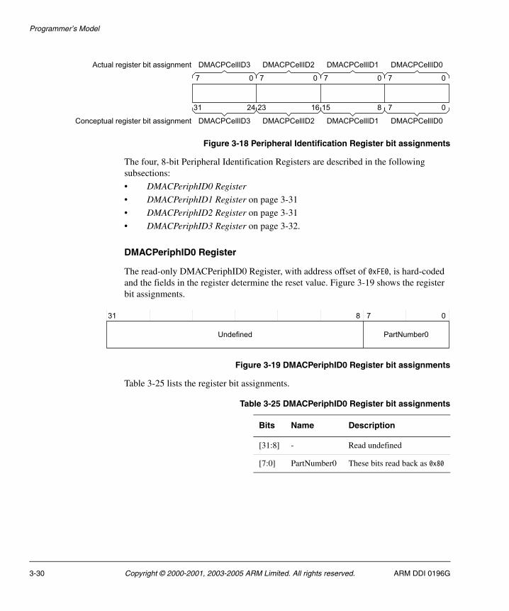
Programmer’s Model
Figure 3-18 Peripheral Identification Register bit assignments
The four, 8-bit Peripheral Identification Registers are described in the following subsections:
• DMACPeriphID0 Register
• DMACPeriphID1 Register on page 3-31
• DMACPeriphID2 Register on page 3-31
• DMACPeriphID3 Register on page 3-32.
DMACPeriphID0 Register
The read-only DMACPeriphID0 Register, with address offset of 0xFE0, is hard-coded and the fields in the register determine the reset value. Figure 3-19 shows the register bit assignments.
Figure 3-19 DMACPeriphID0 Register bit assignments
Table 3-25 lists the register bit assignments.
Table 3-25 DMACPeriphID0 Register bit assignments
Bits Name Description
[31:8] - Read undefined
[7:0] PartNumber0 These bits read back as 0x80
3-30 Copyright © 2000-2001, 2003-2005 ARM Limited. All rights reserved. ARM DDI 0196G
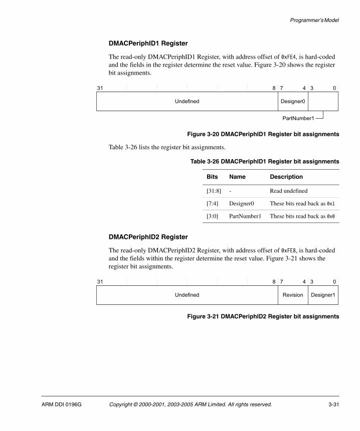
Programmer’s Model
DMACPeriphID1 Register
The read-only DMACPeriphID1 Register, with address offset of 0xFE4, is hard-coded and the fields in the register determine the reset value. Figure 3-20 shows the register bit assignments.
Figure 3-20 DMACPeriphID1 Register bit assignments
Table 3-26 lists the register bit assignments.
DMACPeriphID2 Register
The read-only DMACPeriphID2 Register, with address offset of 0xFE8, is hard-coded and the fields within the register determine the reset value. Figure 3-21 shows the register bit assignments.
Figure 3-21 DMACPeriphID2 Register bit assignments
Table 3-26 DMACPeriphID1 Register bit assignments
Bits Name Description
[31:8] - Read undefined
[7:4] Designer0 These bits read back as 0x1
[3:0] PartNumber1 These bits read back as 0x0
ARM DDI 0196G Copyright © 2000-2001, 2003-2005 ARM Limited. All rights reserved. 3-31
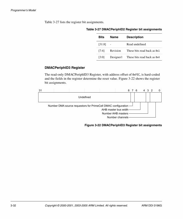
Programmer’s Model
Table 3-27 lists the register bit assignments.
DMACPeriphID3 Register
The read-only DMACPeriphID3 Register, with address offset of 0xFEC, is hard-coded and the fields in the register determine the reset value. Figure 3-22 shows the register bit assignments.
Figure 3-22 DMACPeriphID3 Register bit assignments
Table 3-27 DMACPeriphID2 Register bit assignments
Bits Name Description
[31:8] - Read undefined
[7:4] Revision These bits read back as 0x1
[3:0] Designer1 These bits read back as 0x4
3-32 Copyright © 2000-2001, 2003-2005 ARM Limited. All rights reserved. ARM DDI 0196G
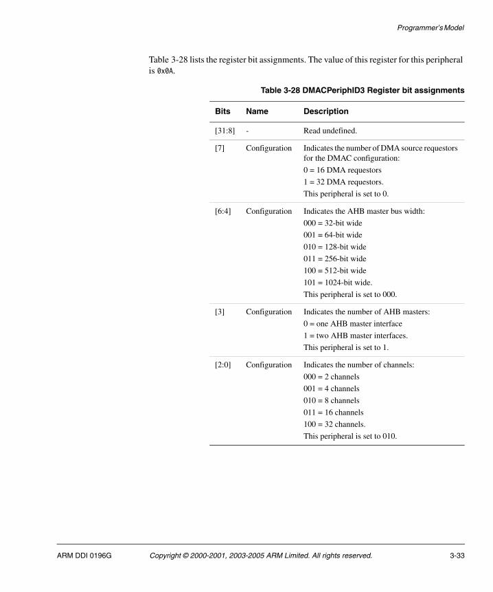
Programmer’s Model
Table 3-28 lists the register bit assignments. The value of this register for this peripheral is 0x0A.
Table 3-28 DMACPeriphID3 Register bit assignments
Bits Name Description
[31:8] - Read undefined.
[7] Configuration Indicates the number of DMA source requestors for the DMAC configuration:
0 = 16 DMA requestors
1 = 32 DMA requestors.
This peripheral is set to 0.
[6:4] Configuration Indicates the AHB master bus width:
000 = 32-bit wide
001 = 64-bit wide
010 = 128-bit wide
011 = 256-bit wide
100 = 512-bit wide
101 = 1024-bit wide.
This peripheral is set to 000.
[3] Configuration Indicates the number of AHB masters:
0 = one AHB master interface
1 = two AHB master interfaces.
This peripheral is set to 1.
[2:0] Configuration Indicates the number of channels:
000 = 2 channels
001 = 4 channels
010 = 8 channels
011 = 16 channels
100 = 32 channels.
This peripheral is set to 010.
ARM DDI 0196G Copyright © 2000-2001, 2003-2005 ARM Limited. All rights reserved. 3-33
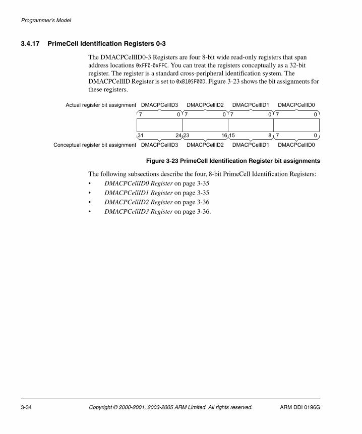
Programmer’s Model
3.4.17 PrimeCell Identification Registers 0-3
The DMACPCellID0-3 Registers are four 8-bit wide read-only registers that span address locations 0xFF0-0xFFC. You can treat the registers conceptually as a 32-bit register. The register is a standard cross-peripheral identification system. The DMACPCellID Register is set to 0xB105F00D. Figure 3-23 shows the bit assignments for these registers.
Figure 3-23 PrimeCell Identification Register bit assignments
The following subsections describe the four, 8-bit PrimeCell Identification Registers:
• DMACPCellID0 Register on page 3-35
• DMACPCellID1 Register on page 3-35
• DMACPCellID2 Register on page 3-36
• DMACPCellID3 Register on page 3-36.
3-34 Copyright © 2000-2001, 2003-2005 ARM Limited. All rights reserved. ARM DDI 0196G
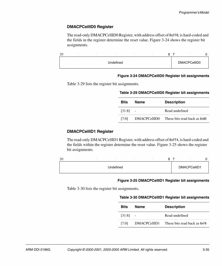
Programmer’s Model
DMACPCellID0 Register
The read-only DMACPCellID0 Register, with address offset of 0xFF0, is hard-coded and the fields in the register determine the reset value. Figure 3-24 shows the register bit assignments.
Figure 3-24 DMACPCellID0 Register bit assignments
Table 3-29 lists the register bit assignments.
DMACPCellID1 Register
The read-only DMACPCellID1 Register, with address offset of 0xFF4, is hard-coded and the fields within the register determine the reset value. Figure 3-25 shows the register bit assignments.
Figure 3-25 DMACPCellID1 Register bit assignments
Table 3-30 lists the register bit assignments.
Table 3-29 DMACPCellID0 Register bit assignments
Bits Name Description
[31:8] - Read undefined
[7:0] DMACPCellID0 These bits read back as 0x0D
Table 3-30 DMACPCellID1 Register bit assignments
Bits Name Description
[31:8] - Read undefined
[7:0] DMACPCellID1 These bits read back as 0xF0
ARM DDI 0196G Copyright © 2000-2001, 2003-2005 ARM Limited. All rights reserved. 3-35
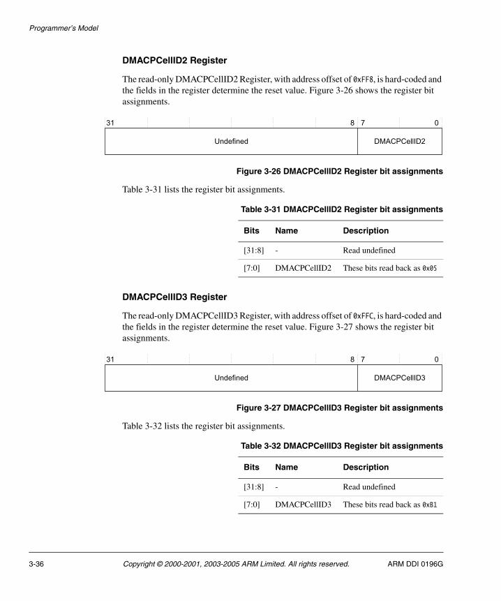
Programmer’s Model
DMACPCellID2 Register
The read-only DMACPCellID2 Register, with address offset of 0xFF8, is hard-coded and the fields in the register determine the reset value. Figure 3-26 shows the register bit assignments.
Figure 3-26 DMACPCellID2 Register bit assignments
Table 3-31 lists the register bit assignments.
DMACPCellID3 Register
The read-only DMACPCellID3 Register, with address offset of 0xFFC, is hard-coded and the fields in the register determine the reset value. Figure 3-27 shows the register bit assignments.
Figure 3-27 DMACPCellID3 Register bit assignments
Table 3-32 lists the register bit assignments.
Table 3-31 DMACPCellID2 Register bit assignments
Bits Name Description
[31:8] - Read undefined
[7:0] DMACPCellID2 These bits read back as 0x05
Table 3-32 DMACPCellID3 Register bit assignments
Bits Name Description
[31:8] - Read undefined
[7:0] DMACPCellID3 These bits read back as 0xB1
3-36 Copyright © 2000-2001, 2003-2005 ARM Limited. All rights reserved. ARM DDI 0196G
Programmer’s Model
3.5 Address generation
Address generation can be either incrementing or non-incrementing.
Note Address wrapping is not supported.
Bursts do not cross the 1KB address boundary.
ARM DDI 0196G Copyright © 2000-2001, 2003-2005 ARM Limited. All rights reserved. 3-37
Programmer’s Model
3.6 Scatter/gather
Scatter/gather is supported through the use of linked lists. This means that the source and destination areas do not have to occupy contiguous areas in memory. You must set the DMACCxLLI Register to 0 if you do not require scatter/gather. For more information about scatter/gather DMA, see Appendix B DMA Interface.
3.6.1 Linked list items
An LLI consists of four words. These words are organized in the following order:
1. DMACCxSrcAddr.
2. DMACCxDestAddr.
3. DMACCxLLI.
4. DMACCxControl.
Note The DMACCxConfiguration Channel Configuration Register is not part of the LLI.
3.6.2 Programming the DMAC for scatter/gather DMA
To program the DMAC for scatter/gather DMA:
1. Write the LLIs for the complete DMA transfer to memory. Each LLI contains four words:
• source address
• destination address
• pointer to next LLI
• control word.
The last LLI has its linked list word pointer set to 0.
2. Choose a free DMA channel with the required priority.
DMA channel 0 has the highest priority and DMA channel 7 the lowest priority.
3. Write the first LLI, previously written to memory, to the relevant channel in the DMAC.
4. Write the channel configuration information to the channel configuration register and set the Channel Enable bit.
The DMAC then transfers the first and then subsequent packets of data as each LLI is loaded.
3-38 Copyright © 2000-2001, 2003-2005 ARM Limited. All rights reserved. ARM DDI 0196G
Programmer’s Model
5. An interrupt can be generated at the end of each LLI depending on the Terminal Count bit in the DMACCxControl Register. If this bit is set, an interrupt is generated at the end of the relevant LLI. You must then service the interrupt request, and you must set the relevant bit in the DMACIntTCClear Register to clear the interrupt.
If so, you must service this interrupt request and you must set the relevant IntTCClear bit in the DMACIntTCClr Register to clear the interrupt request interrupt.
ARM DDI 0196G Copyright © 2000-2001, 2003-2005 ARM Limited. All rights reserved. 3-39
Programmer’s Model
3.7 Interrupt requests
Interrupt requests can be generated when an AHB error is encountered, or at the end of a transfer, terminal count, after all the data corresponding to the current LLI has been transferred to the destination. The interrupts can be masked by programming the relevant bits on the relevant DMACCxControl and DMACCxConfiguration Channel Registers.
Interrupt Status Registers are provided. They group the interrupt requests from all the DMA channels prior to interrupt masking, DMACRawIntTCStatus, DMACRawIntErrorStatus, and after interrupt masking, DMACIntTCStatus, DMACIntErrorStatus.
The DMACIntStatus Register combines both the DMACIntTCStatus and DMACIntErrorStatus requests into a single register to enable the source of an interrupt to be found quickly. Writing to the DMACIntTCClear or the DMACIntErrClr Registers with a bit set HIGH enables selective clearing of interrupts.
The DMAC provides two interrupt request connection schemes. See Interrupt controller connectivity on page 2-16. The simplest connection scheme has a combined error and end of transfer complete interrupt request. To find the source of an interrupt, you must read both the DMACIntStatus and DMACIntTCStatus Registers.
For faster interrupt response, you can use an alternate connection scheme. This scheme uses separate interrupt requests for the error and transfer complete requests. Read either the DMACIntTCStatus or DMACIntErrorStatus Registers to find the source of an interrupt.
3.7.1 Combined terminal count and error interrupt sequence flow
When you use the DMACINTR interrupt request:
1. You must wait until the combined interrupt request from the DMAC goes active.
Assuming the interrupt is enabled in the interrupt controller and in the processor, the processor branches to the interrupt vector address and enters the interrupt service routine.
2. You must read the interrupt controller Status Register and determine whether the source of the request was the DMAC.
3. You must read the DMACIntStatus Register to determine the channel that generated the interrupt.
If more than one request is active, it is recommended that you check the highest priority channels first.
3-40 Copyright © 2000-2001, 2003-2005 ARM Limited. All rights reserved. ARM DDI 0196G

Programmer’s Model
4. You must read the DMACIntTCStatus Register to determine whether the interrupt was generated because of the end of the transfer, terminal count, or because an error occurred.
A HIGH bit indicates that the transfer completed.
5. You must read the DMACIntErrorStatus Register to determine whether the interrupt was generated because of the end of the transfer, terminal count, or because an error occurred.
A HIGH bit indicates that an error occurred.
6. You must write a 1 to the relevant bit in the DMACIntTCClear, or DMACIntErrClr, Register to clear the interrupt request.
3.7.2 Terminal count interrupt sequence flow
When the separate, DMACINTTC and DMACINTERR, interrupt requests are used:
1. You must wait until the terminal count DMA interrupt request goes active.
Assuming the interrupt is enabled in the interrupt controller and in the processor, the processor branches to the interrupt vector address and enters the interrupt service routine.
2. You must read the interrupt controller Status Register to determine if the source of the interrupt request was the DMAC asserting the DMACINTTC signal.
3. You must read the DMACIntTCStatus Register to determine the channel that generated the interrupt.
If more than one request is active, it is recommended that you service the highest priority channel first.
4. You must service the interrupt request.
5. You must write a 1 to the relevant bit in the DMACIntTCClear Register to clear the interrupt request.
3.7.3 Error interrupt sequence flow
When the separate interrupt requests, DMACINTTC and DMACINTERR, are used:
1. You must wait until the interrupt request goes active because of a DMA channel error.
Assuming the interrupt is enabled in the interrupt controller and in the processor, the processor branches to the interrupt vector address and enters the interrupt service routine.
ARM DDI 0196G Copyright © 2000-2001, 2003-2005 ARM Limited. All rights reserved. 3-41
Programmer’s Model
2. You must read the Interrupt Controllers Status Register to determine if the source of the request was the DMAC asserting the DMACINTERR signal.
3. You must read the DMACIntErrorStatus Register to determine the channel that generated the interrupt.
If more than one request is active it is recommended that you check the highest priority channels first.
4. You must service the interrupt request.
5. You must write a 1 to the relevant bit in the DMACIntErrClr Register to clear the interrupt request.
3.7.4 Interrupt polling sequence flow
The DMAC interrupt request signal is masked out, disabled in the interrupt controller, or disabled in the processor. When polling the DMAC, you must:
1. Read the DMACIntStatus Register.
If none of the bits are HIGH repeat this step, otherwise, go to step 2.
If more than one request is active, it is recommended that you check the highest priority channels first.
2. Read the DMACIntTCStatus Register to determine if the interrupt was generated because of the end of the transfer, terminal count, or because of error occurred.
A HIGH bit indicates that the transfer completed.
3. Service the interrupt request.
4. For an error interrupt, write a 1 to the relevant bit of the DMACIntErrClr Register to clear the interrupt request.
For a terminal count interrupt, write a 1 to the relevant bit of the DMACIntTCClr Register.
3-42 Copyright © 2000-2001, 2003-2005 ARM Limited. All rights reserved. ARM DDI 0196G
Programmer’s Model
3.8 DMAC data flow
This section describes the DMAC data flow sequences for:
• Memory-to-memory DMA flow
• Memory-to-peripheral, or peripheral-to-memory DMA flow on page 3-44
• Peripheral-to-peripheral DMA flow on page 3-45.
3.8.1 Memory-to-memory DMA flow
For a memory-to-memory DMA flow:
1. Program and enable the DMA channel.
2. Transfer data whenever the DMA channel has the highest pending priority and the DMAC gains bus master ship of the AHB bus.
3. If an error occurs while transferring the data, generate an error interrupt and disable the DMA stream.
4. Decrement the transfer count.
5. If the count has reached zero:
a. Generate a terminal count interrupt. You can mask the interrupt.
b. If the DMACCxLLI Register is not 0, then reload the following registers and go to back to step 2:
DMACCxSrcAddr
DMACCxDestAddr
DMACCxLLI
DMACCxControl.
However, if DMACCxLLI is 0, the DMA stream is disabled and the flow sequence ends.
ARM DDI 0196G Copyright © 2000-2001, 2003-2005 ARM Limited. All rights reserved. 3-43
Programmer’s Model
3.8.2 Memory-to-peripheral, or peripheral-to-memory DMA flow
For a peripheral-to-memory or memory-to-peripheral DMA flow:
1. Program and enable the DMA channel.
2. Wait for a DMA request.
3. The DMAC then starts transferring data when:
a. The DMA request goes active.
b. The DMA stream has the highest pending priority.
c. The DMAC is the bus master of the AHB bus.
4. If an error occurs while transferring the data, an error interrupt is generated and the DMA stream is disabled, and the flow sequence ends.
5. Decrement the transfer count if the DMAC is controlling the flow control.
6. If the transfer has completed, indicated by the transfer count reaching 0 if the DMAC is performing flow control, or by the peripheral setting the DMACLBREQ or DMACLSREQ signals if the peripheral is performing flow control:
a. The DMAC asserts the DMACTC signal.
b. The terminal count interrupt is generated. You can mask this interrupt.
c. If the DMACCxLLI Register is not 0, then reload the following registers and go to back to step 2:
DMACCxSrcAddr
DMACCxDestAddr
DMACCxLLI
DMACCxControl.
However, if DMACCxLLI is 0, the DMA stream is disabled and the flow sequence ends.
3-44 Copyright © 2000-2001, 2003-2005 ARM Limited. All rights reserved. ARM DDI 0196G
Programmer’s Model
3.8.3 Peripheral-to-peripheral DMA flow
For a peripheral-to-peripheral DMA flow:
1. Program and enable the DMA channel.
2. Wait for a source DMA request.
3. The DMAC then starts transferring data when:
a. The DMA request goes active.
b. The DMA stream has the highest pending priority.
c. The DMAC is the bus master of the AHB bus.
4. If an error occurs while transferring the data, an error interrupt is generated, then finishes.
5. Decrement the transfer count if the DMAC is controlling the flow control.
6. If the transfer has completed, indicated by the transfer count reaching 0 if the DMAC is performing flow control, or by the peripheral setting the DMACLBREQ or DMACLSREQ signals if the peripheral is performing flow control:
a. The DMAC asserts the DMACTC signal to the source peripheral.
b. Subsequent source DMA requests are ignored.
7. When the destination DMA request goes active and there is data in the DMAC FIFO, transfer data into the destination peripheral.
8. If an error occurs while transferring the data, an error interrupt is generated and the DMA stream is disabled, and the flow sequence ends.
9. If the transfer has completed, it is indicated by the transfer count reaching 0 if the DMAC is performing flow control, or by the peripheral setting the DMACLBREQ or DMACLSREQ signals if the peripheral is performing flow control. The following happens:
a. The DMAC asserts the DMACTC signal to the destination peripheral.
b. The terminal count interrupt is generated. You can mask this interrupt.
c. If the DMACCxLLI Register is not 0, then reload the following registers and go to back to step 2:
DMACCxSrcAddr
DMACCxDestAddr
DMACCxLLI
DMACCxControl.
ARM DDI 0196G Copyright © 2000-2001, 2003-2005 ARM Limited. All rights reserved. 3-45
Programmer’s Model
However, if DMACCxLLI is 0, the DMA stream is disabled and the flow sequence ends.
3-46 Copyright © 2000-2001, 2003-2005 ARM Limited. All rights reserved. ARM DDI 0196G
Chapter 4 Programmer’s Model for Test
This chapter describes the additional logic for integration testing. It contains the following sections:
• DMAC test harness overview on page 4-2
• Scan testing on page 4-3
• Test registers on page 4-4
• Integration test on page 4-7.
ARM DDI 0196G Copyright © 2000-2001, 2003-2005 ARM Limited. All rights reserved. 4-1
Programmer’s Model for Test
4.1 DMAC test harness overview
The additional logic for functional verification and integration vectors enables:
• capture of input signals to the block
• stimulation of the output signals.
The integration vectors provide a way of verifying that the DMAC is correctly wired into a system. This is done by separately testing two groups of signals:
AMBA signals
Test these by checking the connections of all the address data bits.
Intra-chip signals, such as interrupt sources
The tests for these signals are system-specific, and enable you to write the necessary tests. Additional logic is implemented that enables you to read/write to each intra-chip input/output signal.
Test registers control these test features. This enables you to test the DMAC in isolation from the rest of the system using only transfers from the AMBA AHB.
4-2 Copyright © 2000-2001, 2003-2005 ARM Limited. All rights reserved. ARM DDI 0196G
Programmer’s Model for Test
4.2 Scan testing
The DMAC is designed to simplify:
• insertion of scan test cells
• use of Automatic Test Pattern Generation (ATPG).
This is the recommended method of manufacturing test.
ARM DDI 0196G Copyright © 2000-2001, 2003-2005 ARM Limited. All rights reserved. 4-3
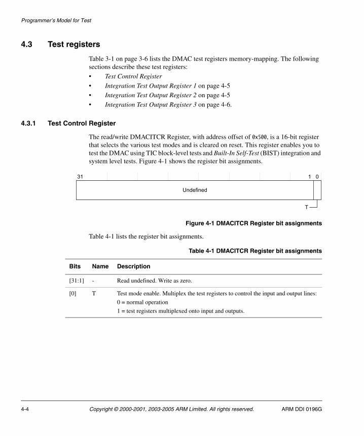
Programmer’s Model for Test
4.3 Test registers
Table 3-1 on page 3-6 lists the DMAC test registers memory-mapping. The following sections describe these test registers:
• Test Control Register
• Integration Test Output Register 1 on page 4-5
• Integration Test Output Register 2 on page 4-5
• Integration Test Output Register 3 on page 4-6.
4.3.1 Test Control Register
The read/write DMACITCR Register, with address offset of 0x500, is a 16-bit register that selects the various test modes and is cleared on reset. This register enables you to test the DMAC using TIC block-level tests and Built-In Self-Test (BIST) integration and system level tests. Figure 4-1 shows the register bit assignments.
Figure 4-1 DMACITCR Register bit assignments
Table 4-1 lists the register bit assignments.
Table 4-1 DMACITCR Register bit assignments
Bits Name Description
[31:1] - Read undefined. Write as zero.
[0] T Test mode enable. Multiplex the test registers to control the input and output lines:
0 = normal operation
1 = test registers multiplexed onto input and outputs.
4-4 Copyright © 2000-2001, 2003-2005 ARM Limited. All rights reserved. ARM DDI 0196G
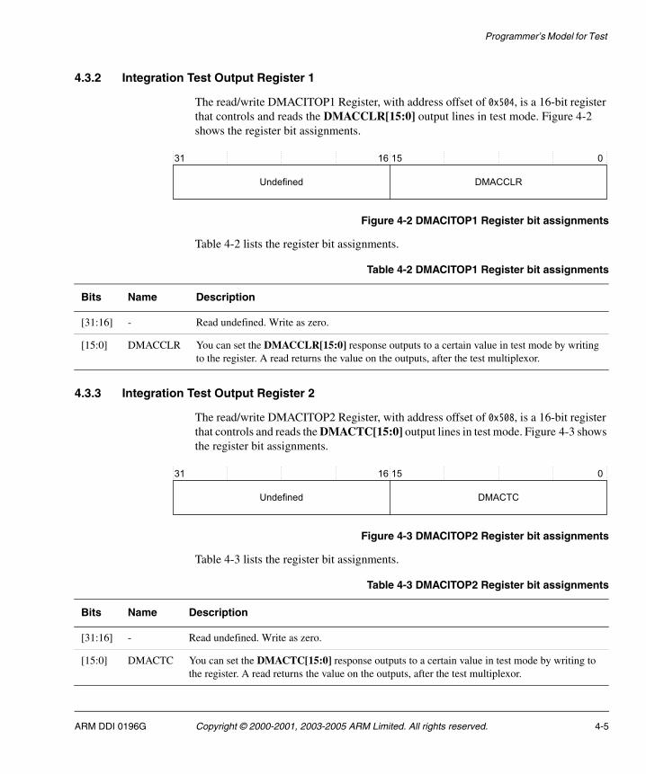
Programmer’s Model for Test
4.3.2 Integration Test Output Register 1
The read/write DMACITOP1 Register, with address offset of 0x504, is a 16-bit register that controls and reads the DMACCLR[15:0] output lines in test mode. Figure 4-2 shows the register bit assignments.
Figure 4-2 DMACITOP1 Register bit assignments
Table 4-2 lists the register bit assignments.
4.3.3 Integration Test Output Register 2
The read/write DMACITOP2 Register, with address offset of 0x508, is a 16-bit register that controls and reads the DMACTC[15:0] output lines in test mode. Figure 4-3 shows the register bit assignments.
Figure 4-3 DMACITOP2 Register bit assignments
Table 4-3 lists the register bit assignments.
Table 4-2 DMACITOP1 Register bit assignments
Bits Name Description
[31:16] - Read undefined. Write as zero.
[15:0] DMACCLR You can set the DMACCLR[15:0] response outputs to a certain value in test mode by writing to the register. A read returns the value on the outputs, after the test multiplexor.
Table 4-3 DMACITOP2 Register bit assignments
Bits Name Description
[31:16] - Read undefined. Write as zero.
[15:0] DMACTC You can set the DMACTC[15:0] response outputs to a certain value in test mode by writing to the register. A read returns the value on the outputs, after the test multiplexor.
ARM DDI 0196G Copyright © 2000-2001, 2003-2005 ARM Limited. All rights reserved. 4-5
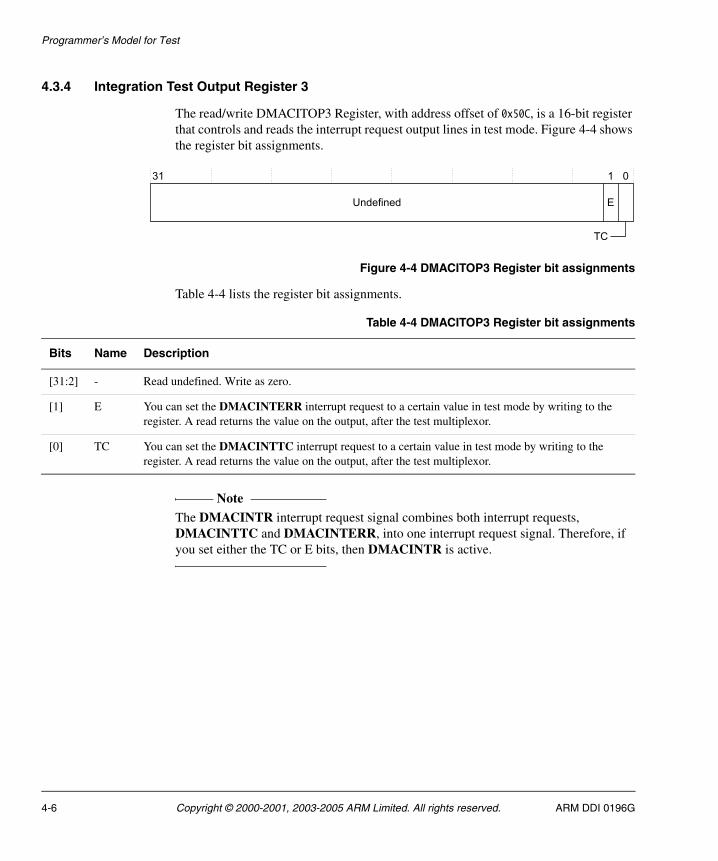
Programmer’s Model for Test
4.3.4 Integration Test Output Register 3
The read/write DMACITOP3 Register, with address offset of 0x50C, is a 16-bit register that controls and reads the interrupt request output lines in test mode. Figure 4-4 shows the register bit assignments.
Figure 4-4 DMACITOP3 Register bit assignments
Table 4-4 lists the register bit assignments.
Note The DMACINTR interrupt request signal combines both interrupt requests, DMACINTTC and DMACINTERR, into one interrupt request signal. Therefore, if you set either the TC or E bits, then DMACINTR is active.
Table 4-4 DMACITOP3 Register bit assignments
Bits Name Description
[31:2] - Read undefined. Write as zero.
[1] E You can set the DMACINTERR interrupt request to a certain value in test mode by writing to the register. A read returns the value on the output, after the test multiplexor.
[0] TC You can set the DMACINTTC interrupt request to a certain value in test mode by writing to the register. A read returns the value on the output, after the test multiplexor.
4-6 Copyright © 2000-2001, 2003-2005 ARM Limited. All rights reserved. ARM DDI 0196G
Programmer’s Model for Test
4.4 Integration test
You can set the non-AMBA intra-chip input signals to certain values, and you can read the output signals using test registers. You can use the Test Control Register, DMACITCR, to set the test multiplexors into test mode.
4.4.1 Input signals
You can set and read the input signals as follows:
DMACxBREQ[15:0]
Set this signal by using the DMACSoftBReq Register. You can read the status of the DMACxBREQ inputs after being combined with SoftBReq by reading the DMACSoftBReq Register.
DMACxSREQ[15:0]
Set this signal by using the DMACSoftSReq Register. You can read the status of the DMACxSREQ inputs after being combined with SoftSReq by reading the DMACSoftSReq Register.
DMACxLBREQ[15:0]
Set this signal by using the DMACSoftLBReq Register. You can read the status of the DMACxLBREQ inputs after being combined with SoftLBReq by reading the DMACSoftLBReq Register.
DMACxLSREQ[15:0]
Set this signal by using the DMACSoftLSReq Register. You can read the status of the DMACxLSREQ inputs after being combined with SoftLSReq by reading the DMACSoftLSReq Register.
4.4.2 Output signals
You can set and read the output signals as follows:
DMACxCLR[15:0]
Set this signal by writing to the DMACITOP1 Register. A read returns the value on the outputs after the test multiplexor.
DMACxTC[15:0]
Set this signal by writing to the DMACITOP2 Register. A read returns the value on the outputs after the test multiplexor.
ARM DDI 0196G Copyright © 2000-2001, 2003-2005 ARM Limited. All rights reserved. 4-7
Programmer’s Model for Test
DMACINTERR
Set this signal by writing to the DMACITOP3 Register. A read returns the value on the outputs after the test multiplexor.
DMACINTTC
Set this signal by writing to the DMACITOP3 Register. A read returns the value on the outputs after the test multiplexor.
4-8 Copyright © 2000-2001, 2003-2005 ARM Limited. All rights reserved. ARM DDI 0196G
Appendix A Signal Descriptions
This appendix describes the signals that interface with the DMAC. It contains the following sections:
• DMA interrupt request signals on page A-2
• DMA request and response signals on page A-3
• AHB slave signals on page A-4
• AHB master signals on page A-6
• AHB master bus request signals on page A-8
• Scan test control signals on page A-9.
ARM DDI 0196G Copyright © 2000-2001, 2003-2005 ARM Limited. All rights reserved. A-1
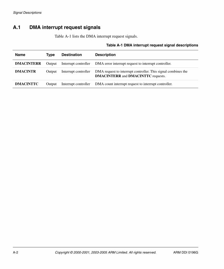
Signal Descriptions
A.1 DMA interrupt request signals
Table A-1 lists the DMA interrupt request signals.
Table A-1 DMA interrupt request signal descriptions
Name Type Destination Description
DMACINTERR Output Interrupt controller DMA error interrupt request to interrupt controller.
DMACINTR Output Interrupt controller DMA request to interrupt controller. This signal combines the DMACINTERR and DMACINTTC requests.
DMACINTTC Output Interrupt controller DMA count interrupt request to interrupt controller.
A-2 Copyright © 2000-2001, 2003-2005 ARM Limited. All rights reserved. ARM DDI 0196G
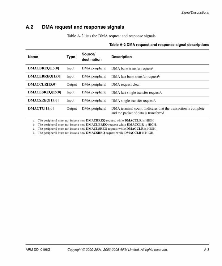
Signal Descriptions
A.2 DMA request and response signals
Table A-2 lists the DMA request and response signals.
Table A-2 DMA request and response signal descriptions
Name TypeSource/destination
Description
DMACBREQ[15:0] Input DMA peripheral DMA burst transfer requesta.
DMACLBREQ[15:0] Input DMA peripheral DMA last burst transfer requestb.
DMACCLR[15:0] Output DMA peripheral DMA request clear.
DMACLSREQ[15:0] Input DMA peripheral DMA last single transfer requestc.
DMACSREQ[15:0] Input DMA peripheral DMA single transfer requestd.
DMACTC[15:0] Output DMA peripheral DMA terminal count. Indicates that the transaction is complete, and the packet of data is transferred.
a. The peripheral must not issue a new DMACBREQ request while DMACCLR is HIGH.b. The peripheral must not issue a new DMACLBREQ request while DMACCLR is HIGH.c. The peripheral must not issue a new DMACLSREQ request while DMACCLR is HIGH.d. The peripheral must not issue a new DMACSREQ request while DMACCLR is HIGH.
ARM DDI 0196G Copyright © 2000-2001, 2003-2005 ARM Limited. All rights reserved. A-3
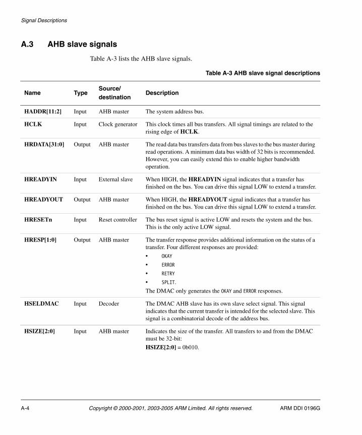
Signal Descriptions
A.3 AHB slave signals
Table A-3 lists the AHB slave signals.
Table A-3 AHB slave signal descriptions
Name TypeSource/destination
Description
HADDR[11:2] Input AHB master The system address bus.
HCLK Input Clock generator This clock times all bus transfers. All signal timings are related to the rising edge of HCLK.
HRDATA[31:0] Output AHB master The read data bus transfers data from bus slaves to the bus master during read operations. A minimum data bus width of 32 bits is recommended. However, you can easily extend this to enable higher bandwidth operation.
HREADYIN Input External slave When HIGH, the HREADYIN signal indicates that a transfer has finished on the bus. You can drive this signal LOW to extend a transfer.
HREADYOUT Output AHB master When HIGH, the HREADYOUT signal indicates that a transfer has finished on the bus. You can drive this signal LOW to extend a transfer.
HRESETn Input Reset controller The bus reset signal is active LOW and resets the system and the bus. This is the only active LOW signal.
HRESP[1:0] Output AHB master The transfer response provides additional information on the status of a transfer. Four different responses are provided:
• OKAY
• ERROR
• RETRY
• SPLIT.
The DMAC only generates the OKAY and ERROR responses.
HSELDMAC Input Decoder The DMAC AHB slave has its own slave select signal. This signal indicates that the current transfer is intended for the selected slave. This signal is a combinatorial decode of the address bus.
HSIZE[2:0] Input AHB master Indicates the size of the transfer. All transfers to and from the DMAC must be 32-bit:
HSIZE[2:0] = 0b010.
A-4 Copyright © 2000-2001, 2003-2005 ARM Limited. All rights reserved. ARM DDI 0196G

Signal Descriptions
HTRANS Input AHB master Transfer type. Four different transfer types are provided:
• IDLE
• BUSY
• NONSEQUENTIAL
• SEQUENTIAL.
You must connect this signal to HTRANS[1] on the AHB interface. HTRANS[0] is not used.
HWDATA[31:0] Input AHB master The write data bus transfers data from the master to the bus slaves during write operations. A minimum data bus width of 32 bits is recommended. However, you can easily extend this to enable higher bandwidth operation.
HWRITE Input AHB master Transfer direction. When HIGH, this signal indicates a write transfer. When LOW, it indicates a read transfer.
Table A-3 AHB slave signal descriptions (continued)
Name TypeSource/destination
Description
ARM DDI 0196G Copyright © 2000-2001, 2003-2005 ARM Limited. All rights reserved. A-5
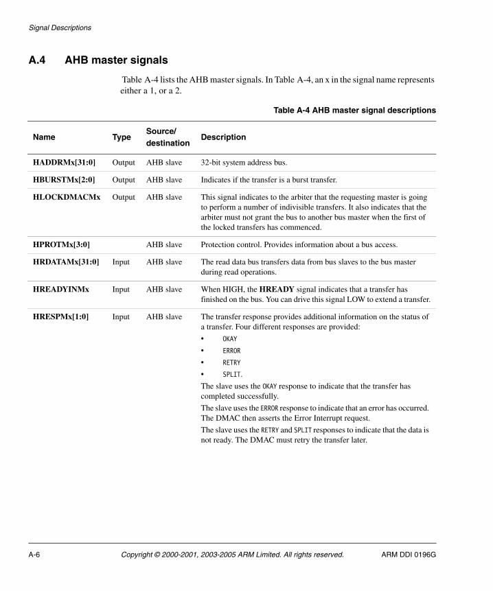
Signal Descriptions
A.4 AHB master signals
Table A-4 lists the AHB master signals. In Table A-4, an x in the signal name represents either a 1, or a 2.
Table A-4 AHB master signal descriptions
Name TypeSource/destination
Description
HADDRMx[31:0] Output AHB slave 32-bit system address bus.
HBURSTMx[2:0] Output AHB slave Indicates if the transfer is a burst transfer.
HLOCKDMACMx Output AHB slave This signal indicates to the arbiter that the requesting master is going to perform a number of indivisible transfers. It also indicates that the arbiter must not grant the bus to another bus master when the first of the locked transfers has commenced.
HPROTMx[3:0] AHB slave Protection control. Provides information about a bus access.
HRDATAMx[31:0] Input AHB slave The read data bus transfers data from bus slaves to the bus master during read operations.
HREADYINMx Input AHB slave When HIGH, the HREADY signal indicates that a transfer has finished on the bus. You can drive this signal LOW to extend a transfer.
HRESPMx[1:0] Input AHB slave The transfer response provides additional information on the status of a transfer. Four different responses are provided:
• OKAY
• ERROR
• RETRY
• SPLIT.
The slave uses the OKAY response to indicate that the transfer has completed successfully.
The slave uses the ERROR response to indicate that an error has occurred. The DMAC then asserts the Error Interrupt request.
The slave uses the RETRY and SPLIT responses to indicate that the data is not ready. The DMAC must retry the transfer later.
A-6 Copyright © 2000-2001, 2003-2005 ARM Limited. All rights reserved. ARM DDI 0196G
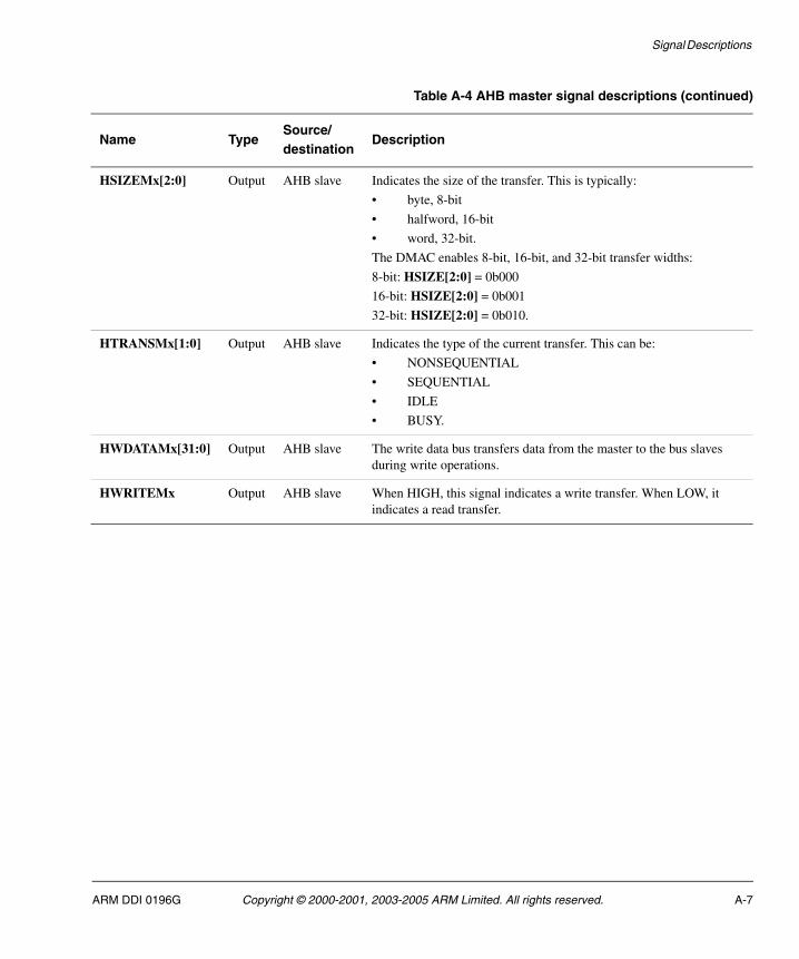
Signal Descriptions
HSIZEMx[2:0] Output AHB slave Indicates the size of the transfer. This is typically:
• byte, 8-bit
• halfword, 16-bit
• word, 32-bit.
The DMAC enables 8-bit, 16-bit, and 32-bit transfer widths:
8-bit: HSIZE[2:0] = 0b000
16-bit: HSIZE[2:0] = 0b001
32-bit: HSIZE[2:0] = 0b010.
HTRANSMx[1:0] Output AHB slave Indicates the type of the current transfer. This can be:
• NONSEQUENTIAL
• SEQUENTIAL
• IDLE
• BUSY.
HWDATAMx[31:0] Output AHB slave The write data bus transfers data from the master to the bus slaves during write operations.
HWRITEMx Output AHB slave When HIGH, this signal indicates a write transfer. When LOW, it indicates a read transfer.
Table A-4 AHB master signal descriptions (continued)
Name TypeSource/destination
Description
ARM DDI 0196G Copyright © 2000-2001, 2003-2005 ARM Limited. All rights reserved. A-7
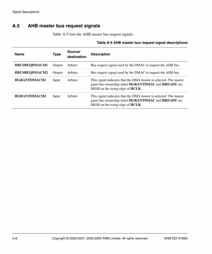
Signal Descriptions
A.5 AHB master bus request signals
Table A-5 lists the AHB master bus request signals.
Table A-5 AHB master bus request signal descriptions
Name TypeSource/destination
Description
HBUSREQDMACM1 Output Arbiter Bus request signal used by the DMAC to request the AHB bus.
HBUSREQDMACM2 Output Arbiter Bus request signal used by the DMAC to request the AHB bus.
HGRANTDMACM1 Input Arbiter This signal indicates that the DMA master is selected. The master gains bus ownership when HGRANTDMAC and HREADY are HIGH on the rising edge of HCLK.
HGRANTDMACM2 Input Arbiter This signal indicates that the DMA master is selected. The master gains bus ownership when HGRANTDMAC and HREADY are HIGH on the rising edge of HCLK.
A-8 Copyright © 2000-2001, 2003-2005 ARM Limited. All rights reserved. ARM DDI 0196G
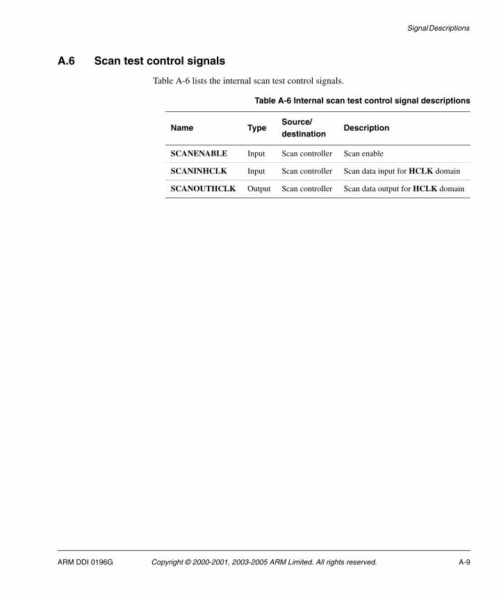
Signal Descriptions
A.6 Scan test control signals
Table A-6 lists the internal scan test control signals.
Table A-6 Internal scan test control signal descriptions
Name TypeSource/destination
Description
SCANENABLE Input Scan controller Scan enable
SCANINHCLK Input Scan controller Scan data input for HCLK domain
SCANOUTHCLK Output Scan controller Scan data output for HCLK domain
ARM DDI 0196G Copyright © 2000-2001, 2003-2005 ARM Limited. All rights reserved. A-9
Signal Descriptions
A-10 Copyright © 2000-2001, 2003-2005 ARM Limited. All rights reserved. ARM DDI 0196G
Appendix B DMA Interface
This section describes the DMA request and response interface. It contains the following sections:
• DMA request signals on page B-2
• DMA response signals on page B-3
• Flow control on page B-4
• Transfer types on page B-5
• Signal timing on page B-17
• Functional timing diagram on page B-18
• DMAC transfer timing diagram on page B-19.
ARM DDI 0196G Copyright © 2000-2001, 2003-2005 ARM Limited. All rights reserved. B-1
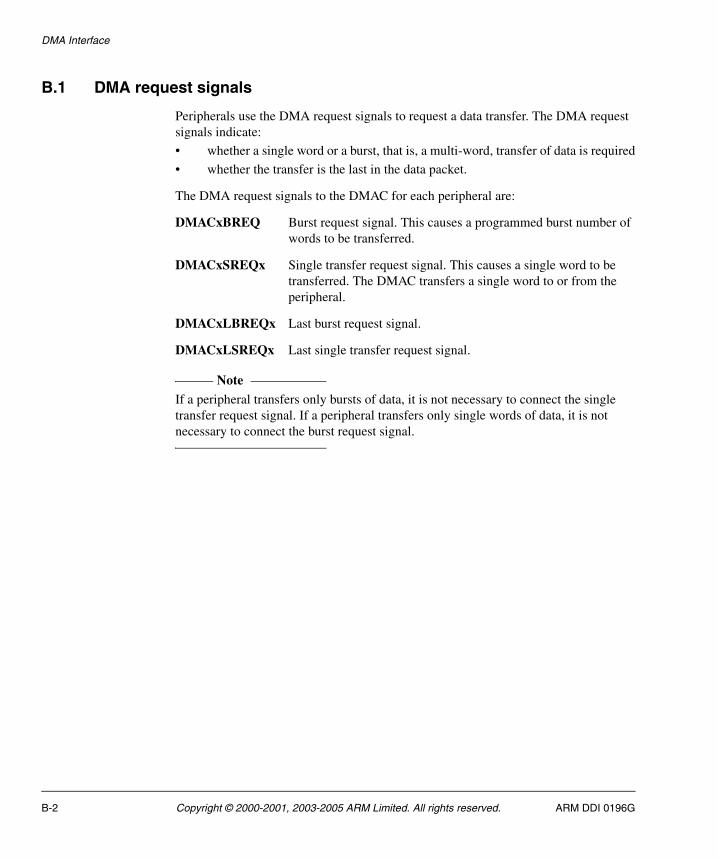
DMA Interface
B.1 DMA request signals
Peripherals use the DMA request signals to request a data transfer. The DMA request signals indicate:
• whether a single word or a burst, that is, a multi-word, transfer of data is required
• whether the transfer is the last in the data packet.
The DMA request signals to the DMAC for each peripheral are:
DMACxBREQ Burst request signal. This causes a programmed burst number of words to be transferred.
DMACxSREQx Single transfer request signal. This causes a single word to be transferred. The DMAC transfers a single word to or from the peripheral.
DMACxLBREQx Last burst request signal.
DMACxLSREQx Last single transfer request signal.
Note If a peripheral transfers only bursts of data, it is not necessary to connect the single transfer request signal. If a peripheral transfers only single words of data, it is not necessary to connect the burst request signal.
B-2 Copyright © 2000-2001, 2003-2005 ARM Limited. All rights reserved. ARM DDI 0196G
DMA Interface
B.2 DMA response signals
The DMA response signals indicate whether the transfer initiated by the DMA request signal has completed. You can use the response signals to indicate whether a complete packet has been transferred.
The DMA response signals from the DMAC for each peripheral are:
DMACxCLRx DMA clear or acknowledge signal. The DMAC uses this signal to acknowledge a DMA request from the peripheral.
DMACxTC DMA terminal count signal. The DMAC uses this signal to indicate to the peripheral that the DMA transfer is complete.
Note Some peripherals do not require connection to the DMA terminal count signal.
ARM DDI 0196G Copyright © 2000-2001, 2003-2005 ARM Limited. All rights reserved. B-3
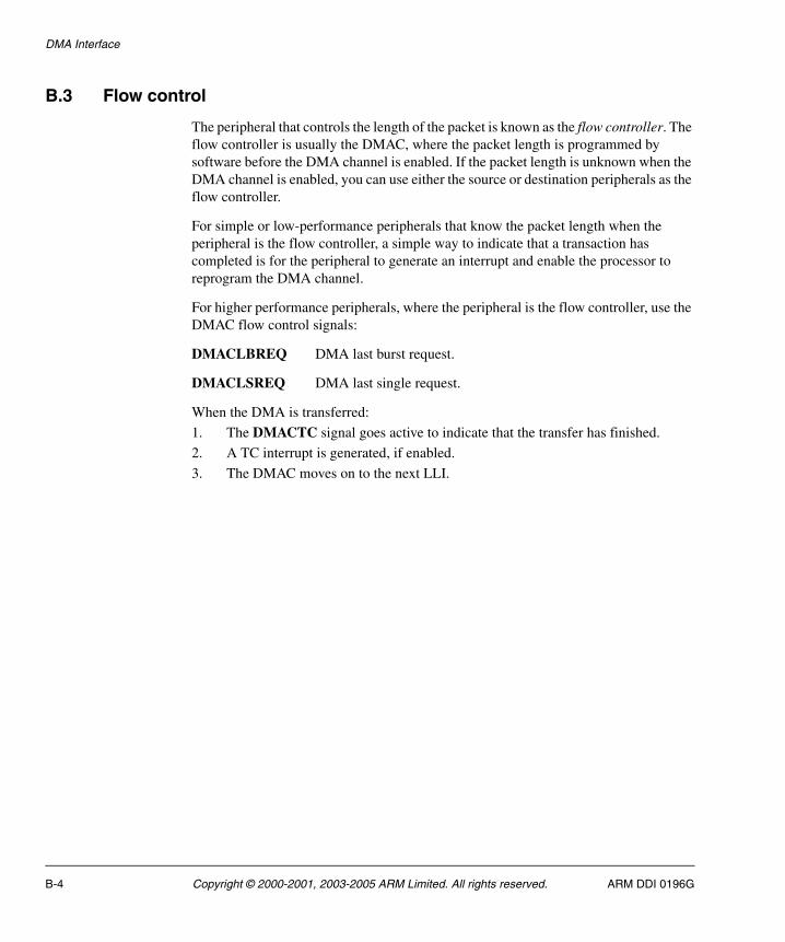
DMA Interface
B.3 Flow control
The peripheral that controls the length of the packet is known as the flow controller. The flow controller is usually the DMAC, where the packet length is programmed by software before the DMA channel is enabled. If the packet length is unknown when the DMA channel is enabled, you can use either the source or destination peripherals as the flow controller.
For simple or low-performance peripherals that know the packet length when the peripheral is the flow controller, a simple way to indicate that a transaction has completed is for the peripheral to generate an interrupt and enable the processor to reprogram the DMA channel.
For higher performance peripherals, where the peripheral is the flow controller, use the DMAC flow control signals:
DMACLBREQ DMA last burst request.
DMACLSREQ DMA last single request.
When the DMA is transferred:
1. The DMACTC signal goes active to indicate that the transfer has finished.
2. A TC interrupt is generated, if enabled.
3. The DMAC moves on to the next LLI.
B-4 Copyright © 2000-2001, 2003-2005 ARM Limited. All rights reserved. ARM DDI 0196G
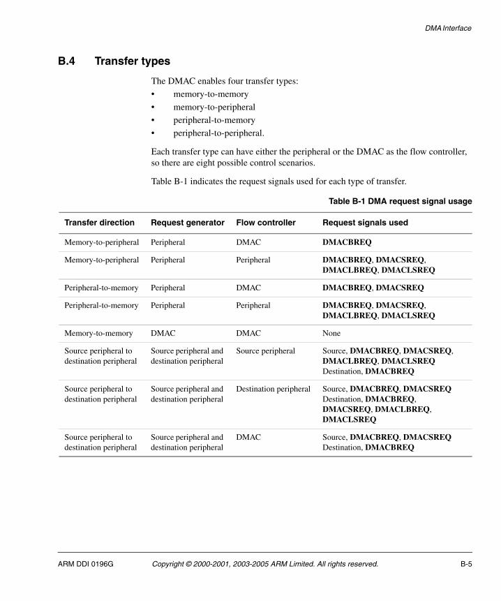
DMA Interface
B.4 Transfer types
The DMAC enables four transfer types:
• memory-to-memory
• memory-to-peripheral
• peripheral-to-memory
• peripheral-to-peripheral.
Each transfer type can have either the peripheral or the DMAC as the flow controller, so there are eight possible control scenarios.
Table B-1 indicates the request signals used for each type of transfer.
Table B-1 DMA request signal usage
Transfer direction Request generator Flow controller Request signals used
Memory-to-peripheral Peripheral DMAC DMACBREQ
Memory-to-peripheral Peripheral Peripheral DMACBREQ, DMACSREQ, DMACLBREQ, DMACLSREQ
Peripheral-to-memory Peripheral DMAC DMACBREQ, DMACSREQ
Peripheral-to-memory Peripheral Peripheral DMACBREQ, DMACSREQ, DMACLBREQ, DMACLSREQ
Memory-to-memory DMAC DMAC None
Source peripheral to destination peripheral
Source peripheral and destination peripheral
Source peripheral Source, DMACBREQ, DMACSREQ, DMACLBREQ, DMACLSREQ Destination, DMACBREQ
Source peripheral to destination peripheral
Source peripheral and destination peripheral
Destination peripheral Source, DMACBREQ, DMACSREQ Destination, DMACBREQ, DMACSREQ, DMACLBREQ, DMACLSREQ
Source peripheral to destination peripheral
Source peripheral and destination peripheral
DMAC Source, DMACBREQ, DMACSREQ Destination, DMACBREQ
ARM DDI 0196G Copyright © 2000-2001, 2003-2005 ARM Limited. All rights reserved. B-5
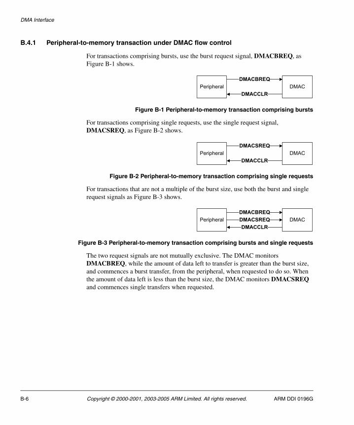
DMA Interface
B.4.1 Peripheral-to-memory transaction under DMAC flow control
For transactions comprising bursts, use the burst request signal, DMACBREQ, as Figure B-1 shows.
Figure B-1 Peripheral-to-memory transaction comprising bursts
For transactions comprising single requests, use the single request signal, DMACSREQ, as Figure B-2 shows.
Figure B-2 Peripheral-to-memory transaction comprising single requests
For transactions that are not a multiple of the burst size, use both the burst and single request signals as Figure B-3 shows.
Figure B-3 Peripheral-to-memory transaction comprising bursts and single requests
The two request signals are not mutually exclusive. The DMAC monitors DMACBREQ, while the amount of data left to transfer is greater than the burst size, and commences a burst transfer, from the peripheral, when requested to do so. When the amount of data left is less than the burst size, the DMAC monitors DMACSREQ and commences single transfers when requested.
B-6 Copyright © 2000-2001, 2003-2005 ARM Limited. All rights reserved. ARM DDI 0196G
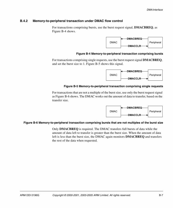
DMA Interface
B.4.2 Memory-to-peripheral transaction under DMAC flow control
For transactions comprising bursts, use the burst request signal, DMACBREQ, as Figure B-4 shows.
Figure B-4 Memory-to-peripheral transaction comprising bursts
For transactions comprising single requests, use the burst request signal DMACBREQ, and set the burst size to 1. Figure B-5 shows this signal.
Figure B-5 Memory-to-peripheral transaction comprising single requests
For transactions that are not a multiple of the burst size, use only the burst request signal as Figure B-6 shows. The DMAC works out the amount of data to transfer, based on the transfer size.
Figure B-6 Memory-to-peripheral transaction comprising bursts that are not multiples of the burst size
Only DMACBREQ is required. The DMAC transfers full bursts of data while the amount of data left to transfer is greater than the burst size. When the amount of data left is less than the burst size, the DMAC again monitors DMACBREQ and transfers the rest of the data when requested.
ARM DDI 0196G Copyright © 2000-2001, 2003-2005 ARM Limited. All rights reserved. B-7
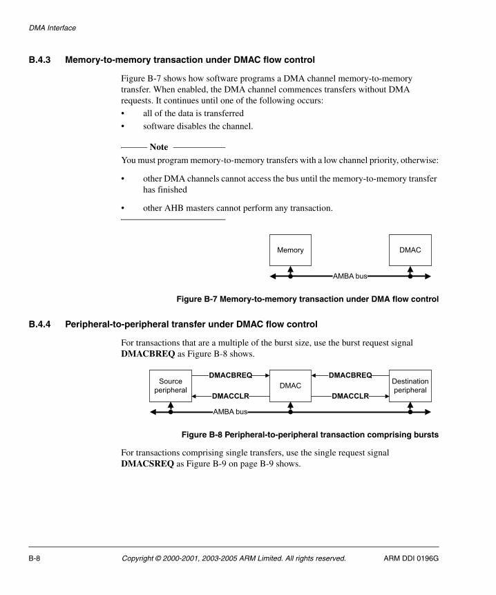
DMA Interface
B.4.3 Memory-to-memory transaction under DMAC flow control
Figure B-7 shows how software programs a DMA channel memory-to-memory transfer. When enabled, the DMA channel commences transfers without DMA requests. It continues until one of the following occurs:
• all of the data is transferred
• software disables the channel.
Note You must program memory-to-memory transfers with a low channel priority, otherwise:
• other DMA channels cannot access the bus until the memory-to-memory transfer has finished
• other AHB masters cannot perform any transaction.
Figure B-7 Memory-to-memory transaction under DMA flow control
B.4.4 Peripheral-to-peripheral transfer under DMAC flow control
For transactions that are a multiple of the burst size, use the burst request signal DMACBREQ as Figure B-8 shows.
Figure B-8 Peripheral-to-peripheral transaction comprising bursts
For transactions comprising single transfers, use the single request signal DMACSREQ as Figure B-9 on page B-9 shows.
B-8 Copyright © 2000-2001, 2003-2005 ARM Limited. All rights reserved. ARM DDI 0196G
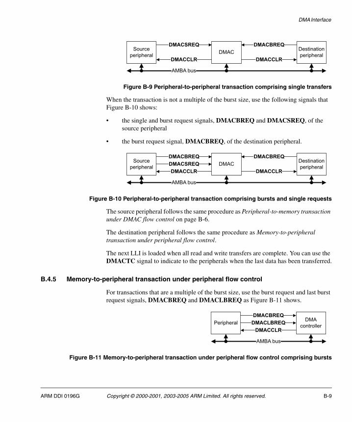
DMA Interface
Figure B-9 Peripheral-to-peripheral transaction comprising single transfers
When the transaction is not a multiple of the burst size, use the following signals that Figure B-10 shows:
• the single and burst request signals, DMACBREQ and DMACSREQ, of the source peripheral
• the burst request signal, DMACBREQ, of the destination peripheral.
Figure B-10 Peripheral-to-peripheral transaction comprising bursts and single requests
The source peripheral follows the same procedure as Peripheral-to-memory transaction under DMAC flow control on page B-6.
The destination peripheral follows the same procedure as Memory-to-peripheral transaction under peripheral flow control.
The next LLI is loaded when all read and write transfers are complete. You can use the DMACTC signal to indicate to the peripherals when the last data has been transferred.
B.4.5 Memory-to-peripheral transaction under peripheral flow control
For transactions that are a multiple of the burst size, use the burst request and last burst request signals, DMACBREQ and DMACLBREQ as Figure B-11 shows.
Figure B-11 Memory-to-peripheral transaction under peripheral flow control comprising bursts
ARM DDI 0196G Copyright © 2000-2001, 2003-2005 ARM Limited. All rights reserved. B-9
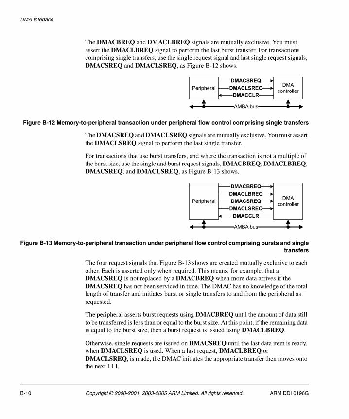
DMA Interface
The DMACBREQ and DMACLBREQ signals are mutually exclusive. You must assert the DMACLBREQ signal to perform the last burst transfer. For transactions comprising single transfers, use the single request signal and last single request signals, DMACSREQ and DMACLSREQ, as Figure B-12 shows.
Figure B-12 Memory-to-peripheral transaction under peripheral flow control comprising single transfers
The DMACSREQ and DMACLSREQ signals are mutually exclusive. You must assert the DMACLSREQ signal to perform the last single transfer.
For transactions that use burst transfers, and where the transaction is not a multiple of the burst size, use the single and burst request signals, DMACBREQ, DMACLBREQ, DMACSREQ, and DMACLSREQ, as Figure B-13 shows.
Figure B-13 Memory-to-peripheral transaction under peripheral flow control comprising bursts and singletransfers
The four request signals that Figure B-13 shows are created mutually exclusive to each other. Each is asserted only when required. This means, for example, that a DMACSREQ is not replaced by a DMACBREQ when more data arrives if the DMACSREQ has not been serviced in time. The DMAC has no knowledge of the total length of transfer and initiates burst or single transfers to and from the peripheral as requested.
The peripheral asserts burst requests using DMACBREQ until the amount of data still to be transferred is less than or equal to the burst size. At this point, if the remaining data is equal to the burst size, then a burst request is issued using DMACLBREQ.
Otherwise, single requests are issued on DMACSREQ until the last data item is ready, when DMACLSREQ is used. When a last request, DMACLBREQ or DMACLSREQ, is made, the DMAC initiates the appropriate transfer then moves onto the next LLI.
B-10 Copyright © 2000-2001, 2003-2005 ARM Limited. All rights reserved. ARM DDI 0196G
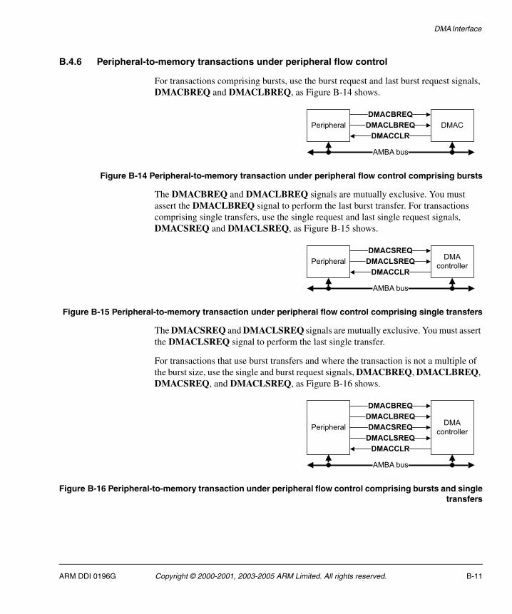
DMA Interface
B.4.6 Peripheral-to-memory transactions under peripheral flow control
For transactions comprising bursts, use the burst request and last burst request signals, DMACBREQ and DMACLBREQ, as Figure B-14 shows.
Figure B-14 Peripheral-to-memory transaction under peripheral flow control comprising bursts
The DMACBREQ and DMACLBREQ signals are mutually exclusive. You must assert the DMACLBREQ signal to perform the last burst transfer. For transactions comprising single transfers, use the single request and last single request signals, DMACSREQ and DMACLSREQ, as Figure B-15 shows.
Figure B-15 Peripheral-to-memory transaction under peripheral flow control comprising single transfers
The DMACSREQ and DMACLSREQ signals are mutually exclusive. You must assert the DMACLSREQ signal to perform the last single transfer.
For transactions that use burst transfers and where the transaction is not a multiple of the burst size, use the single and burst request signals, DMACBREQ, DMACLBREQ, DMACSREQ, and DMACLSREQ, as Figure B-16 shows.
Figure B-16 Peripheral-to-memory transaction under peripheral flow control comprising bursts and singletransfers
ARM DDI 0196G Copyright © 2000-2001, 2003-2005 ARM Limited. All rights reserved. B-11
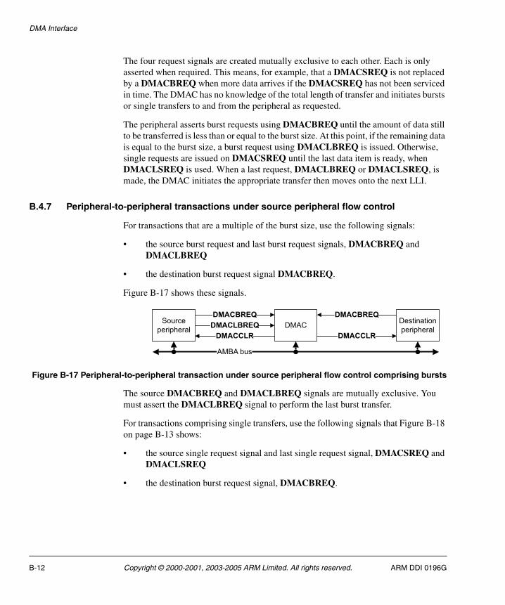
DMA Interface
The four request signals are created mutually exclusive to each other. Each is only asserted when required. This means, for example, that a DMACSREQ is not replaced by a DMACBREQ when more data arrives if the DMACSREQ has not been serviced in time. The DMAC has no knowledge of the total length of transfer and initiates bursts or single transfers to and from the peripheral as requested.
The peripheral asserts burst requests using DMACBREQ until the amount of data still to be transferred is less than or equal to the burst size. At this point, if the remaining data is equal to the burst size, a burst request using DMACLBREQ is issued. Otherwise, single requests are issued on DMACSREQ until the last data item is ready, when DMACLSREQ is used. When a last request, DMACLBREQ or DMACLSREQ, is made, the DMAC initiates the appropriate transfer then moves onto the next LLI.
B.4.7 Peripheral-to-peripheral transactions under source peripheral flow control
For transactions that are a multiple of the burst size, use the following signals:
• the source burst request and last burst request signals, DMACBREQ and DMACLBREQ
• the destination burst request signal DMACBREQ.
Figure B-17 shows these signals.
Figure B-17 Peripheral-to-peripheral transaction under source peripheral flow control comprising bursts
The source DMACBREQ and DMACLBREQ signals are mutually exclusive. You must assert the DMACLBREQ signal to perform the last burst transfer.
For transactions comprising single transfers, use the following signals that Figure B-18 on page B-13 shows:
• the source single request signal and last single request signal, DMACSREQ and DMACLSREQ
• the destination burst request signal, DMACBREQ.
B-12 Copyright © 2000-2001, 2003-2005 ARM Limited. All rights reserved. ARM DDI 0196G
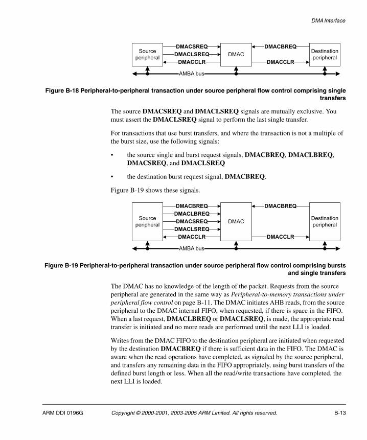
DMA Interface
Figure B-18 Peripheral-to-peripheral transaction under source peripheral flow control comprising singletransfers
The source DMACSREQ and DMACLSREQ signals are mutually exclusive. You must assert the DMACLSREQ signal to perform the last single transfer.
For transactions that use burst transfers, and where the transaction is not a multiple of the burst size, use the following signals:
• the source single and burst request signals, DMACBREQ, DMACLBREQ, DMACSREQ, and DMACLSREQ
• the destination burst request signal, DMACBREQ.
Figure B-19 shows these signals.
Figure B-19 Peripheral-to-peripheral transaction under source peripheral flow control comprising burstsand single transfers
The DMAC has no knowledge of the length of the packet. Requests from the source peripheral are generated in the same way as Peripheral-to-memory transactions under peripheral flow control on page B-11. The DMAC initiates AHB reads, from the source peripheral to the DMAC internal FIFO, when requested, if there is space in the FIFO. When a last request, DMACLBREQ or DMACLSREQ, is made, the appropriate read transfer is initiated and no more reads are performed until the next LLI is loaded.
Writes from the DMAC FIFO to the destination peripheral are initiated when requested by the destination DMACBREQ if there is sufficient data in the FIFO. The DMAC is aware when the read operations have completed, as signaled by the source peripheral, and transfers any remaining data in the FIFO appropriately, using burst transfers of the defined burst length or less. When all the read/write transactions have completed, the next LLI is loaded.
ARM DDI 0196G Copyright © 2000-2001, 2003-2005 ARM Limited. All rights reserved. B-13
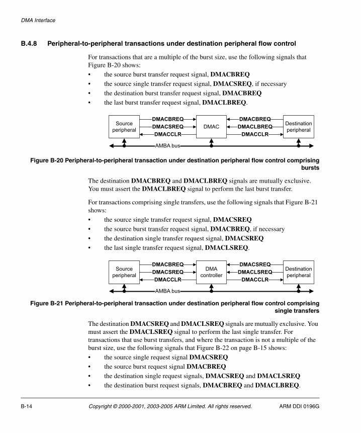
DMA Interface
B.4.8 Peripheral-to-peripheral transactions under destination peripheral flow control
For transactions that are a multiple of the burst size, use the following signals that Figure B-20 shows:
• the source burst transfer request signal, DMACBREQ• the source single transfer request signal, DMACSREQ, if necessary
• the destination burst transfer request signal, DMACBREQ• the last burst transfer request signal, DMACLBREQ.
Figure B-20 Peripheral-to-peripheral transaction under destination peripheral flow control comprisingbursts
The destination DMACBREQ and DMACLBREQ signals are mutually exclusive. You must assert the DMACLBREQ signal to perform the last burst transfer.
For transactions comprising single transfers, use the following signals that Figure B-21 shows:
• the source single transfer request signal, DMACSREQ• the source burst transfer request signal, DMACBREQ, if necessary
• the destination single transfer request signal, DMACSREQ• the last single transfer request signal, DMACLSREQ.
Figure B-21 Peripheral-to-peripheral transaction under destination peripheral flow control comprisingsingle transfers
The destination DMACSREQ and DMACLSREQ signals are mutually exclusive. You must assert the DMACLSREQ signal to perform the last single transfer. For transactions that use burst transfers, and where the transaction is not a multiple of the burst size, use the following signals that Figure B-22 on page B-15 shows:
• the source single request signal DMACSREQ• the source burst request signal DMACBREQ• the destination single request signals, DMACSREQ and DMACLSREQ• the destination burst request signals, DMACBREQ and DMACLBREQ.
B-14 Copyright © 2000-2001, 2003-2005 ARM Limited. All rights reserved. ARM DDI 0196G
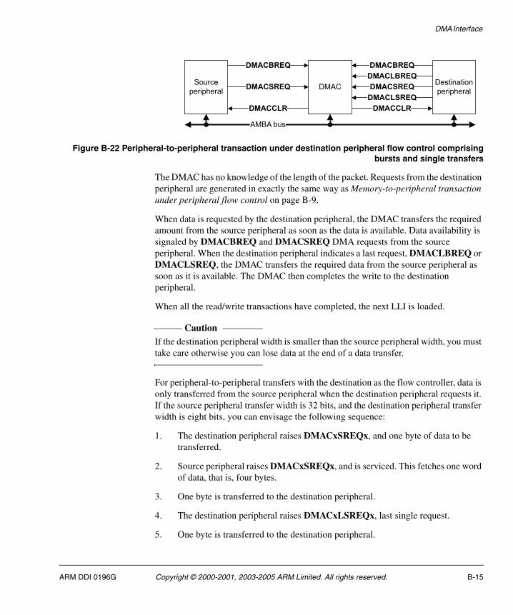
DMA Interface
Figure B-22 Peripheral-to-peripheral transaction under destination peripheral flow control comprisingbursts and single transfers
The DMAC has no knowledge of the length of the packet. Requests from the destination peripheral are generated in exactly the same way as Memory-to-peripheral transaction under peripheral flow control on page B-9.
When data is requested by the destination peripheral, the DMAC transfers the required amount from the source peripheral as soon as the data is available. Data availability is signaled by DMACBREQ and DMACSREQ DMA requests from the source peripheral. When the destination peripheral indicates a last request, DMACLBREQ or DMACLSREQ, the DMAC transfers the required data from the source peripheral as soon as it is available. The DMAC then completes the write to the destination peripheral.
When all the read/write transactions have completed, the next LLI is loaded.
Caution If the destination peripheral width is smaller than the source peripheral width, you must take care otherwise you can lose data at the end of a data transfer.
For peripheral-to-peripheral transfers with the destination as the flow controller, data is only transferred from the source peripheral when the destination peripheral requests it. If the source peripheral transfer width is 32 bits, and the destination peripheral transfer width is eight bits, you can envisage the following sequence:
1. The destination peripheral raises DMACxSREQx, and one byte of data to be transferred.
2. Source peripheral raises DMACxSREQx, and is serviced. This fetches one word of data, that is, four bytes.
3. One byte is transferred to the destination peripheral.
4. The destination peripheral raises DMACxLSREQx, last single request.
5. One byte is transferred to the destination peripheral.
ARM DDI 0196G Copyright © 2000-2001, 2003-2005 ARM Limited. All rights reserved. B-15
DMA Interface
6. The transaction is now complete. Therefore, from the four bytes retrieved from the source peripheral, two are transferred to the destination peripheral, but two more are left in the channel FIFO in the DMAC. This data is then lost.
B-16 Copyright © 2000-2001, 2003-2005 ARM Limited. All rights reserved. ARM DDI 0196G
DMA Interface
B.5 Signal timing
The timing behavior of the DMA signals is as follows:
DMA request signal DMAC{L}(B/S)REQx
Informs the DMAC that a peripheral is ready to proceed with a DMA transfer of the indicated size.
Active HIGH.
Sampled by the DMAC on the positive edge of HCLK. The DMA request signals are used in conjunction with the DMACCLR signal to perform handshaking.
DMA Acknowledge or Clear DMACCLRx
Indicates to the slave that a DMA transfer has completed.
Active HIGH.
DMA Terminal Count DMACTCx
Indicates to the slave that the end of packet has been reached.
Active HIGH.
Note If the DMA request source does not use the same clock as the DMAC, then you must synchronize the request by setting the relevant bit in the DMACSync Register.
ARM DDI 0196G Copyright © 2000-2001, 2003-2005 ARM Limited. All rights reserved. B-17

DMA Interface
B.6 Functional timing diagram
A peripheral asserts a DMA request and holds it active. The DMAC asserts the DMACCLR signal when the last data item has been transferred. When the peripheral sees that the DMACCLR signal has gone active, it takes the DMA request signal inactive. The DMAC deasserts the DMACCLR signal when the DMA request signal goes inactive.
Figure B-23 shows a functional timing diagram of this.
Figure B-23 DMA interface timing
Note It is illegal for a peripheral to give a new DMACSREQ or DMACBREQ signal while DMACCLR is HIGH.
B-18 Copyright © 2000-2001, 2003-2005 ARM Limited. All rights reserved. ARM DDI 0196G
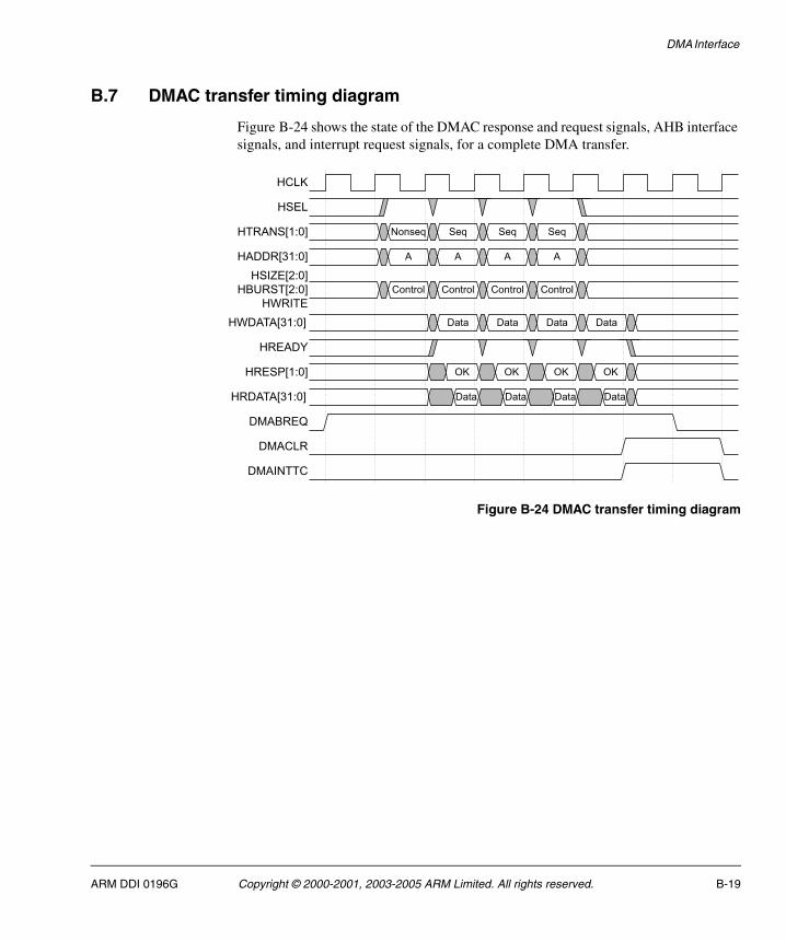
DMA Interface
B.7 DMAC transfer timing diagram
Figure B-24 shows the state of the DMAC response and request signals, AHB interface signals, and interrupt request signals, for a complete DMA transfer.
Figure B-24 DMAC transfer timing diagram
ARM DDI 0196G Copyright © 2000-2001, 2003-2005 ARM Limited. All rights reserved. B-19

DMA Interface
B-20 Copyright © 2000-2001, 2003-2005 ARM Limited. All rights reserved. ARM DDI 0196G

Appendix C Scatter/Gather
This section describes scatter/gather through LLI. It contains the following section:
• Scatter/gather through linked list operation on page C-2.
ARM DDI 0196G Copyright © 2000-2001, 2003-2005 ARM Limited. All rights reserved. C-1
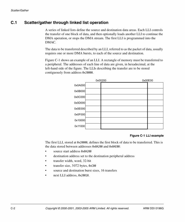
Scatter/Gather
C.1 Scatter/gather through linked list operation
A series of linked lists define the source and destination data areas. Each LLI controls the transfer of one block of data, and then optionally loads another LLI to continue the DMA operation, or stops the DMA stream. The first LLI is programmed into the DMAC.
The data to be transferred described by an LLI, referred to as the packet of data, usually requires one or more DMA bursts, to each of the source and destination.
Figure C-1 shows an example of an LLI. A rectangle of memory must be transferred to a peripheral. The addresses of each line of data are given, in hexadecimal, at the left-hand side of the figure. The LLIs describing the transfer are to be stored contiguously from address 0x20000.
Figure C-1 LLI example
The first LLI, stored at 0x20000, defines the first block of data to be transferred. This is the data stored between addresses 0x0A200 and 0x0AE00:
• source start address 0x0A200
• destination address set to the destination peripheral address
• transfer width, word, 32-bit
• transfer size, 3072 bytes, 0xC00
• source and destination burst sizes, 16 transfers
• next LLI address, 0x20010.
C-2 Copyright © 2000-2001, 2003-2005 ARM Limited. All rights reserved. ARM DDI 0196G
Scatter/Gather
The second LLI, stored at 0x20010, defines the next block of data to be transferred:
• source start address 0x0B200
• destination address set to the destination peripheral address
• transfer width, word, 32-bit
• transfer size, 3072 bytes, 0xC00
• source and destination burst sizes, 16 transfers
• next LLI address, 0x20020.
A chain of descriptors is built up, each one pointing to the next in the series. To initialize the DMA stream, the first LLI, 0x20000, is programmed into the DMAC. When the first packet of data has been transferred, the next LLI is automatically loaded.
The final LLI is stored at 0x20070 and contains:
• source start address 0x11200
• destination address set to the destination peripheral address
• transfer width, word, 32-bit
• transfer size, 3072 bytes, 0xC00
• source and destination burst sizes, 16 transfers
• next LLI address, 0x0.
Because the next LLI address is set to zero, this is the last descriptor, and the DMA channel is disabled after transferring the last item of data. The channel is probably set to generate an interrupt at this point to indicate to the ARM processor that the channel can be reprogrammed.
ARM DDI 0196G Copyright © 2000-2001, 2003-2005 ARM Limited. All rights reserved. C-3
Scatter/Gather
C-4 Copyright © 2000-2001, 2003-2005 ARM Limited. All rights reserved. ARM DDI 0196G
Glossary
This glossary describes some of the terms used in technical documents from ARM Limited.
Abort A mechanism that indicates to a core that the value associated with a memory access is invalid. An abort can be caused by the external or internal memory system as a result of attempting to access invalid instruction or data memory. An abort is classified as either a Prefetch or Data Abort, and an internal or External Abort.
See also Data Abort, External Abort and Prefetch Abort.
Advanced eXtensible Interface (AXI)A bus protocol that supports separate address/control and data phases, unaligned data transfers using byte strobes, burst-based transactions with only start address issued, separate read and write data channels to enable low-cost DMA, ability to issue multiple outstanding addresses, out-of-order transaction completion, and easy addition of register stages to provide timing closure.
The AXI protocol also includes optional extensions to cover signaling for low-power operation.
AXI is targeted at high performance, high clock frequency system designs and includes a number of features that make it very suitable for high speed sub-micron interconnect.
ARM DDI 0196G Copyright © 2000-2001, 2003-2005 ARM Limited. All rights reserved. Glossary-1
Glossary
Advanced High-performance Bus (AHB)A bus protocol with a fixed pipeline between address/control and data phases. It only supports a subset of the functionality provided by the AMBA AXI protocol. The full AMBA AHB protocol specification includes a number of features that are not commonly required for master and slave IP developments and ARM Limited recommends only a subset of the protocol is usually used. This subset is defined as the AMBA AHB-Lite protocol.
See also Advanced Microcontroller Bus Architecture and AHB-Lite.
Advanced Microcontroller Bus Architecture (AMBA)A family of protocol specifications that describe a strategy for the interconnect. AMBA is the ARM open standard for on-chip buses. It is an on-chip bus specification that details a strategy for the interconnection and management of functional blocks that make up a System-on-Chip (SoC). It aids in the development of embedded processors with one or more CPUs or signal processors and multiple peripherals. AMBA complements a reusable design methodology by defining a common backbone for SoC modules.
Advanced Peripheral Bus (APB)A simpler bus protocol than AXI and AHB. It is designed for use with ancillary or general-purpose peripherals such as timers, interrupt controllers, UARTs, and I/O ports. Connection to the main system bus is through a system-to-peripheral bus bridge that helps to reduce system power consumption.
AHB See Advanced High-performance Bus.
AHB-Lite A subset of the full AMBA AHB protocol specification. It provides all of the basic functions required by the majority of AMBA AHB slave and master designs, particularly when used with a multi-layer AMBA interconnect. In most cases, the extra facilities provided by a full AMBA AHB interface are implemented more efficiently by using an AMBA AXI protocol interface.
Aligned A data item stored at an address that is divisible by the number of bytes that defines the data size is said to be aligned. Aligned words and halfwords have addresses that are divisible by four and two respectively. The terms word-aligned and halfword-aligned therefore stipulate addresses that are divisible by four and two respectively.
AMBA See Advanced Microcontroller Bus Architecture.
APB See Advanced Peripheral Bus.
Application Specific Integrated Circuit (ASIC)An integrated circuit that has been designed to perform a specific application function. It can be custom-built or mass-produced.
Glossary-2 Copyright © 2000-2001, 2003-2005 ARM Limited. All rights reserved. ARM DDI 0196G
Glossary
Architecture The organization of hardware and/or software that characterizes a processor and its attached components, and enables devices with similar characteristics to be grouped together when describing their behavior, for example, Harvard architecture, instruction set architecture, ARMv6 architecture.
ARM instruction A word that specifies an operation for an ARM processor to perform. ARM instructions must be word-aligned.
ASIC See Application Specific Integrated Circuit.
ATB bridge A synchronous ATB bridge provides a register slice to facilitate timing closure through the addition of a pipeline stage. It also provides a unidirectional link between two synchronous ATB domains.
An asynchronous ATB bridge provides a unidirectional link between two ATB domains with asynchronous clocks. It is intended to support connection of components with ATB ports residing in different clock domains.
ATPG See Automatic Test Pattern Generation.
Automatic Test Pattern Generation (ATPG)The process of automatically generating manufacturing test vectors for an ASIC design, using a specialized software tool.
AXI See Advanced eXtensible Interface.
Beat Alternative word for an individual transfer within a burst. For example, an INCR4 burst comprises four beats.
See also Burst.
BE-8 Big-endian view of memory in a byte-invariant system.
See also BE-32, LE, Byte-invariant and Word-invariant.
BE-32 Big-endian view of memory in a word-invariant system.
See also BE-8, LE, Byte-invariant and Word-invariant.
Big-endian Byte ordering scheme in which bytes of decreasing significance in a data word are stored at increasing addresses in memory.
See also Little-endian and Endianness.
ARM DDI 0196G Copyright © 2000-2001, 2003-2005 ARM Limited. All rights reserved. Glossary-3
Glossary
Big-endian memory Memory in which:
• a byte or halfword at a word-aligned address is the most significant byte or halfword within the word at that address
• a byte at a halfword-aligned address is the most significant byte within the halfword at that address.
See also Little-endian memory.
Block address An address that comprises a tag, an index, and a word field. The tag bits identify the way that contains the matching cache entry for a cache hit. The index bits identify the set being addressed. The word field contains the word address that can be used to identify specific words, halfwords, or bytes within the cache entry.
See also Cache terminology diagram on the last page of this glossary.
Burst A group of transfers to consecutive addresses. Because the addresses are consecutive, there is no requirement to supply an address for any of the transfers after the first one. This increases the speed at which the group of transfers can occur. Bursts over AMBA are controlled using signals to indicate the length of the burst and how the addresses are incremented.
See also Beat.
Byte An 8-bit data item.
Cache A block of on-chip or off-chip fast access memory locations, situated between the processor and main memory, used for storing and retrieving copies of often used instructions and/or data. This is done to greatly increase the average speed of memory accesses and so improve processor performance.
See also Cache terminology diagram on the last page of this glossary.
Cache hit A memory access that can be processed at high speed because the instruction or data that it addresses is already held in the cache.
Cache line The basic unit of storage in a cache. It is always a power of two words in size (usually four or eight words), and is required to be aligned to a suitable memory boundary.
See also Cache terminology diagram on the last page of this glossary.
Cache miss A memory access that cannot be processed at high speed because the instruction/data it addresses is not in the cache and a main memory access is required.
Cache set A cache set is a group of cache lines (or blocks). A set contains all the ways that can be addressed with the same index. The number of cache sets is always a power of two.
See also Cache terminology diagram on the last page of this glossary.
Glossary-4 Copyright © 2000-2001, 2003-2005 ARM Limited. All rights reserved. ARM DDI 0196G
Glossary
Cache way A group of cache lines (or blocks). It is 2 to the power of the number of index bits in size.
See also Cache terminology diagram on the last page of this glossary.
Cold reset Also known as power-on reset. Starting the processor by turning power on. Turning power off and then back on again clears main memory and many internal settings. Some program failures can lock up the processor and require a cold reset to enable the system to be used again. In other cases, only a warm reset is required.
See also Warm reset.
Coprocessor A processor that supplements the main processor. It carries out additional functions that the main processor cannot perform. Usually used for floating-point math calculations, signal processing, or memory management.
Core A core is that part of a processor that contains the ALU, the datapath, the general-purpose registers, the Program Counter, and the instruction decode and control circuitry.
CoreSight The infrastructure for monitoring, tracing, and debugging a complete system on chip.
Data Abort An indication from a memory system to the core of an attempt to access an illegal data memory location. An exception must be taken if the processor attempts to use the data that caused the abort.
See also Abort, External Abort, and Prefetch Abort.
Data cache A block of on-chip fast access memory locations, situated between the processor and main memory, used for storing and retrieving copies of often used data. This is done to greatly increase the average speed of memory accesses and so improve processor performance.
Direct Memory Access (DMA)An operation that accesses main memory directly, without the processor performing any accesses to the data concerned.
DMA See Direct Memory Access.
Endianness Byte ordering. The scheme that determines the order that successive bytes of a data word are stored in memory. An aspect of the system’s memory mapping.
See also Little-endian and Big-endian
Event 1 (Simple) An observable condition that can be used by an ETM to control aspects of a trace.
2 (Complex) A boolean combination of simple events that is used by an ETM to control aspects of a trace.
ARM DDI 0196G Copyright © 2000-2001, 2003-2005 ARM Limited. All rights reserved. Glossary-5
Glossary
Exception A fault or error event that is considered serious enough to require that program execution is interrupted. Examples include attempting to perform an invalid memory access, external interrupts, and undefined instructions. When an exception occurs, normal program flow is interrupted and execution is resumed at the corresponding exception vector. This contains the first instruction of the interrupt handler to deal with the exception.
Exception vector See Interrupt vector.
External Abort An indication from an external memory system to a core that the value associated with a memory access is invalid. An external abort is caused by the external memory system as a result of attempting to access invalid memory.
See also Abort, Data Abort and Prefetch Abort.
Fast context switchIn a multitasking system, the point at which the time-slice allocated to one process stops and the one for the next process starts. If processes are switched often enough, they can appear to a user to be running in parallel, in addition to being able to respond quicker to external events that might affect them.
In ARM processors, a fast context switch is caused by the selection of a non-zero PID value to switch the context to that of the next process. A fast context switch causes each Virtual Address for a memory access, generated by the ARM processor, to produce a Modified Virtual Address that is sent to the rest of the memory system to be used in place of a normal Virtual Address. For some cache control operations Virtual Addresses are passed to the memory system as data. In these cases no address modification takes place.
Fraction The floating-point field that lies to the right of the implied binary point.
Halfword A 16-bit data item.
High vectors Alternative locations for exception vectors. The high vector address range is near the top of the address space, rather than at the bottom.
Ignore (IGN) Must ignore memory writes.
Index See Cache index.
Instruction cache A block of on-chip fast access memory locations, situated between the processor and main memory, used for storing and retrieving copies of often used instructions. This is done to greatly increase the average speed of memory accesses and so improve processor performance.
Interrupt handler A program that control of the processor is passed to when an interrupt occurs.
Glossary-6 Copyright © 2000-2001, 2003-2005 ARM Limited. All rights reserved. ARM DDI 0196G
Glossary
Interrupt vector One of a number of fixed addresses in low memory, or in high memory if high vectors are configured, that contains the first instruction of the corresponding interrupt handler.
Joint Test Action Group (JTAG)The name of the organization that developed standard IEEE 1149.1. This standard defines a boundary-scan architecture used for in-circuit testing of integrated circuit devices. It is commonly known by the initials JTAG.
JTAG See Joint Test Action Group.
Little-endian Byte ordering scheme in which bytes of increasing significance in a data word are stored at increasing addresses in memory.
See also Big-endian and Endianness.
Little-endian memoryMemory in which:
• a byte or halfword at a word-aligned address is the least significant byte or halfword within the word at that address
• a byte at a halfword-aligned address is the least significant byte within the halfword at that address.
See also Big-endian memory.
Memory Management Unit (MMU)Hardware that controls caches and access permissions to blocks of memory, and translates virtual addresses to physical addresses.
Microprocessor See Processor.
MMU See Memory Management Unit.
Modified Virtual Address (MVA)A Virtual Address produced by the ARM processor can be changed by the current Process ID to provide a Modified Virtual Address (MVA) for the MMUs and caches.
Multi-layer An interconnect scheme similar to a cross-bar switch. Each master on the interconnect has a direct link to each slave, The link is not shared with other masters. This enables each master to process transfers in parallel with other masters. Contention only occurs in a multi-layer interconnect at a payload destination, typically the slave.
Multi-master AHB Typically a shared, not multi-layer, AHB interconnect scheme. More than one master connects to a single AMBA AHB link. In this case, the bus is implemented with a set of full AMBA AHB master interfaces. Masters that use the AMBA AHB-Lite protocol must connect through a wrapper to supply full AMBA AHB master signals to support multi-master operation.
ARM DDI 0196G Copyright © 2000-2001, 2003-2005 ARM Limited. All rights reserved. Glossary-7
Glossary
MVA See Modified Virtual Address.
PA See Physical Address.
Physical Address (PA)The MMU performs a translation on Modified Virtual Addresses (MVA) to produce the Physical Address (PA) that is given to the AMBA bus to perform an external access. The PA is also stored in the data cache to avoid the necessity for address translation when data is cast out of the cache.
See also Fast Context Switch Extension.
Power-on reset See Cold reset.
Prefetching In pipelined processors, the process of fetching instructions from memory to fill up the pipeline before the preceding instructions have finished executing. Prefetching an instruction does not mean that the instruction has to be executed.
Prefetch Abort An indication from a memory system to the core that an instruction has been fetched from an illegal memory location. An exception must be taken if the processor attempts to execute the instruction. A Prefetch Abort can be caused by the external or internal memory system as a result of attempting to access invalid instruction memory.
See also Data Abort, External Abort and Abort.
Processor A processor is the circuitry in a computer system required to process data using the computer instructions. It is an abbreviation of microprocessor. A clock source, power supplies, and main memory are also required to create a minimum complete working computer system.
Read Reads are defined as memory operations that have the semantics of a load. That is, the ARM instructions LDM, LDRD, LDC, LDR, LDRT, LDRSH, LDRH, LDRSB, LDRB, LDRBT, LDREX, RFE, STREX, SWP, and SWPB, and the Thumb instructions LDM, LDR, LDRSH, LDRH, LDRSB, LDRB, and POP.
Java instructions that are accelerated by hardware can cause a number of reads to occur, according to the state of the Java stack and the implementation of the Java hardware acceleration.
Region A partition of instruction or data memory space.
Reserved A field in a control register or instruction format is reserved if the field is to be defined by the implementation, or produces Unpredictable results if the contents of the field are not zero. These fields are reserved for use in future extensions of the architecture or are implementation-specific. All reserved bits not used by the implementation must be written as 0 and read as 0.
SCREG The currently selected scan chain number in an ARM TAP controller.
Glossary-8 Copyright © 2000-2001, 2003-2005 ARM Limited. All rights reserved. ARM DDI 0196G
Glossary
SDF See Standard Delay Format.
Set See Cache set.
Tag The upper portion of a block address used to identify a cache line within a cache. The block address from the CPU is compared with each tag in a set in parallel to determine if the corresponding line is in the cache. If it is, it is said to be a cache hit and the line can be fetched from cache. If the block address does not correspond to any of the tags, it is said to be a cache miss and the line must be fetched from the next level of memory.
See also Cache terminology diagram on the last page of this glossary.
Thumb instruction A halfword that specifies an operation for an ARM processor in Thumb state to perform. Thumb instructions must be halfword-aligned.
Thumb state A processor that is executing Thumb (16-bit) halfword aligned instructions is operating in Thumb state.
Trap An exceptional condition in a VFP coprocessor that has the respective exception enable bit set in the FPSCR register. The user trap handler is executed.
Unaligned A data item stored at an address that is not divisible by the number of bytes that defines the data size is said to be unaligned. For example, a word stored at an address that is not divisible by four.
Undefined Indicates an instruction that generates an Undefined instruction trap. See the ARM Architecture Reference Manual for more details on ARM exceptions.
Unpredictable Means that the behavior of the ETM cannot be relied on. Such conditions have not been validated. When applied to the programming of an event resource, only the output of that event resource is Unpredictable.
Unpredictable behavior can affect the behavior of the entire system, because the ETM is capable of causing the core to enter debug state, and external outputs can be used for other purposes.
Unpredictable For reads, the data returned when reading from this location is unpredictable. It can have any value. For writes, writing to this location causes unpredictable behavior, or an unpredictable change in device configuration. Unpredictable instructions must not halt or hang the processor, or any part of the system.
VA See Virtual Address.
ARM DDI 0196G Copyright © 2000-2001, 2003-2005 ARM Limited. All rights reserved. Glossary-9
Glossary
Virtual Address (VA)The MMU uses its page tables to translate a Virtual Address into a Physical Address. The processor executes code at the Virtual Address, that might be located elsewhere in physical memory.
See also Fast Context Switch Extension, Modified Virtual Address, and Physical Address.
Way See Cache way.
Word A 32-bit data item.
Write Writes are defined as operations that have the semantics of a store. That is, the ARM instructions SRS, STM, STRD, STC, STRT, STRH, STRB, STRBT, STREX, SWP, and SWPB, and the Thumb instructions STM, STR, STRH, STRB, and PUSH.
Java instructions that are accelerated by hardware can cause a number of writes to occur, according to the state of the Java stack and the implementation of the Java hardware acceleration.
Cache terminology diagramThe diagram illustrates the following cache terminology:
• block address
• cache line
• cache set
• cache way
• index
• tag.
Glossary-10 Copyright © 2000-2001, 2003-2005 ARM Limited. All rights reserved. ARM DDI 0196G
Glossary
ARM DDI 0196G Copyright © 2000-2001, 2003-2005 ARM Limited. All rights reserved. Glossary-11

Glossary
Glossary-12 Copyright © 2000-2001, 2003-2005 ARM Limited. All rights reserved. ARM DDI 0196G