printableelasticconductorsby insitu formationof ... printing, traces are dried at 80 c for 1h,...
TRANSCRIPT

ARTICLESPUBLISHED ONLINE: 15 MAY 2017 | DOI: 10.1038/NMAT4904
Printable elastic conductors by in situ formation ofsilver nanoparticles from silver flakesNaoji Matsuhisa1, Daishi Inoue2, Peter Zalar1,3†, Hanbit Jin1, Yorishige Matsuba1,3, Akira Itoh1,3,Tomoyuki Yokota1,3, Daisuke Hashizume2 and Takao Someya1,2,3,4*
Printable elastic conductors promise large-area stretchable sensor/actuator networks for healthcare, wearables and robotics.Elastomers with metal nanoparticles are one of the best approaches to achieve high performance, but large-area utilization islimited by di�culties in their processability. Here we report a printable elastic conductor containing Ag nanoparticles that areformed in situ, solely by mixing micrometre-sized Ag flakes, fluorine rubbers, and surfactant. Our printable elastic compositesexhibit conductivity higher than 4,000S cm−1 (highest value: 6,168 S cm−1) at 0% strain, and 935 S cm−1 when stretched upto 400%. Ag nanoparticle formation is influenced by the surfactant, heating processes, and elastomer molecular weight,resulting in a drastic improvement of conductivity. Fully printed sensor networks for stretchable robots are demonstrated,sensing pressure and temperature accurately, even when stretched over 250%.
Fabrication of large-area stretchable electronic devices isnecessary for future applications in healthcare, wearables, androbotics1–4. For instance, next-generation robots are being
designed with joints and ranges of movement that transcendhumans, which already typically exceed extensions of 100% (ref. 5).To fully integrate devices and sensors, internal wiring has been thepredominant solution. However, the harmonic design of this wiringwith mechanical systems constitutes a great challenge. Therefore,simply patchable or wearable sensor systems are desirable forfuture interfacing with humans or robots. Highly stretchable sensorsystems have high design flexibility and therefore hold promise fornovel applications, such as stretchable prosthetics with the abilityto feel6. The adoption of sensors or actuators to dynamic surfacesrequires the advancement of stretchable electronic devices, and inparticular stretchable wiring.
Stretchable wiring is the most important component in int-egrated stretchable electronics. Obtaining reliable conductanceagainst strain can be achieved by the use of intrinsically stretch-able materials, such as liquid metals7–9, conducting polymers10,11,and ionic conductors12. Another approach is to fabricate conduc-tive pathways using micro-structures, which can be obtained bymainly twomethods.One ismetallization of artificiallymademicro-structures, including serpentine2,13,14, micro- or nano-meshes4,15,16,or accordion motifs17. The other is by self-assembly of structuredconductive pathways, which is advantageous in terms of large-area,low-cost and high-throughput fabrication. This can be achievedusing cracked metal thin films18,19, carbon nanotubes20–23, metalnanowires24,25, metal flakes26–28, and metal nanoparticles29. Usingthese as fillers in a composite with elastomers gives several advan-tages, such as printability, elasticity, and low sheet resistance due tothe ability to form a thick layer. In our previous report, Ag flakeswere dispersed in a fluorinated elastomer. The surface localizationof Ag flakes, driven by the addition of fluorinated surfactant and
water, was crucial for obtaining excellent conductivity retentionunder high strain27. In other approaches, elastic conductors usingAgnanowires have shown very high conductivity between 0 and 200%strain24,25. The use of nanoparticles has yielded the highest con-ductivity at strains larger than 200% (ref. 29). Nanoparticles areknown to possess a unique self-alignment property in responseto their surroundings30, such as mechanical strain29 or electricalfields31. However, the use of nanoparticles in large-area applica-tions is limited by the complicated preparation of both materialsand films.
Here we report a high-performance stretchable and printableelastic conductor realized by the in situ formation of Ag nanopar-ticles (AgNPs), formed by simply printing an ink comprising fluo-rine rubber, fluorine surfactant, Ag flakes, and methylisobutylke-tone (MIBK) as the solvent. (Fig. 1a,b). The initial conductivity is6,168 S cm−1, and the conductivity can remain as high as 935 S cm−1at 400% strain.
In this composite, Ag flakes are used as a cost-competitiveconducting filler. Scanning electron microscopy (SEM) images andthe size distribution of Ag flakes are available in SupplementaryFigs 1 and 2, respectively. The fluorine rubber was chosen for itsstretchability, environmental stability, and high polarity to attractions32. The fluorine-rubber-compatible surfactant is a nonionicpolymeric surfactant consisting of a hydrophilic ethyleneoxidegroup and a fluorophyllic perfluoroalkyl group. MIBK is an organicsolvent used to dissolve the fluorine rubber. The ink’s viscosityis 14.5 Pa s at a shear rate of 10 s−1 (Supplementary Fig. 3). Thisviscosity is suitable for stencil, screen, and dispenser printingmethods. After printing, traces are dried at 80 ◦C for 1 h, followedby additional heating at 120 ◦C for 1 h, which is critical for theformation of AgNPs as described below.
Surprisingly, printing and heating this ink give rise to theremarkable generation of AgNPs from Ag flakes. In the ×3k
1Department of Electrical Engineering and Information Systems, The University of Tokyo, 7-3-1 Hongo, Bunkyo-ku, Tokyo 113-8656, Japan. 2Center forEmergent Matter Science (CEMS), RIKEN, 2-1 Hirosawa, Wako, Saitama 351-0198, Japan. 3Exploratory Research for Advanced Technology (ERATO), JapanScience and Technology Agency (JST), 2-11-16, Yayoi, Bunkyo-ku, Tokyo 113-0032, Japan. 4Thin-Film Device Laboratory, RIKEN, 2-1 Hirosawa, Wako,Saitama 351-0198, Japan. †Present address: Holst Centre/TNO, High Tech Campus 31, 5605 KN Eindhoven, The Netherlands.*e-mail: [email protected]
NATUREMATERIALS | ADVANCE ONLINE PUBLICATION | www.nature.com/naturematerials 1
© 2017 Macmillan Publishers Limited, part of Springer Nature. All rights reserved.

ARTICLES NATUREMATERIALS DOI: 10.1038/NMAT4904
l m n
Elasticconductors
w/o surfactant
Elasticconductors
w/ surfactantand low
temperature
Fluorine rubberand surfactant
a
Elasticconductors
w/ surfactant
Elasticconductors
w/ surfactant
c d e
f g h
i j k
Ag flakes
Fluorine rubber
Ag flakesSurfactant
Methylisobutylketone
b
In situ formedAg nanoparticles
×3k ×100k ×300k
×80k ×200k ×300k
F F
FF
F CF3x y
Mix and print
Ag flake
SEM
TEM
Figure 1 | Printable elastic conductors by in situ formation of silver nanoparticles from silver flakes. a, Fabrication process. b, AgNPs are in situsynthesized just by mixing four components and printing. They form conducting paths with micrometre-sized Ag flakes. c–k, Surface SEM images of elasticconductors without surfactant (c–e) and with surfactant (f–k). Samples f–h are prepared at low temperature (80 ◦C, 1 h). l–n, TEM images of elasticconductors with surfactant. The density of AgNPs available in TEM is higher than that in SEM. This is reasonable because SEM and TEM probe mainly thesurface and the inside of a sample, respectively. Scale bars, 5 µm (c,f,i), 200 nm (d,g,j), 50 nm (e,h,k), 100 nm (l), 50 nm (m), and 20 nm (n).
magnification image of the elastic conductor, micrometre-sized Agflakes are uniformly dispersed in the elastomer (Fig. 1i). Whenzooming in to ×100k or ×300k, a high population of AgNPsare observed between the flakes (Fig. 1j,k). The area fraction ofAgNPs is 10.2%. The size distribution is shown in SupplementaryFig. 4, which shows an average size of 8.1 nm. The presence ofAgNPs (2–10 nm) is further confirmed by cross-sectional SEM(Supplementary Fig. 5) and transmission electron microscopy(TEM) (Fig. 1l–n). The distance between each AgNP is typically2–10 nm. SuchAgNP formation has not been confirmed in previous
reports on elastic conductors utilizing silver flakes21,26,28 although thematerials combination is fairly similar, especially with our previousreports27. This might be because the careful selection of materialsand processing conditions are important for AgNP formation, asdiscussed later.
The formation of AgNPs is confirmed by SEM observations ofelastic conductors in three different conditions; the elastic conductorwith surfactant (Fig. 1i–k), without surfactant (Fig. 1c–e), and withsurfactant but prepared using only one low-temperature dryingprocess (80 ◦C1 h, Fig. 1f–h). The population of AgNPs is noticeably
2
© 2017 Macmillan Publishers Limited, part of Springer Nature. All rights reserved.
NATUREMATERIALS | ADVANCE ONLINE PUBLICATION | www.nature.com/naturematerials

NATUREMATERIALS DOI: 10.1038/NMAT4904 ARTICLESba
dc
fe
104
103
102
101
104
103
102
101
100
0 50 100 150 200 250 300
w/ surfactantw/o surfactantw/ surfactant andlow temperature
Cond
uctiv
ity (S
cm
−1)
Strain (%)
Elastic conductors
104
103
102
0.00 0.05 0.10 0.15 0.20 0.25
0%300%
Cond
uctiv
ity (S
cm
−1)
Surfactant volume fraction
Applied strain
104
102
100
10−2
10−4
0
100
200
300
400
80 100 120 140
Initi
al c
ondu
ctiv
ity (S
cm
−1)
Initi
al c
ondu
ctiv
ity (S
cm
−1)
Stretchability (%)
Temperature (°C)
104
103
102
101
0 100 200 300 400 500
Cond
uctiv
ity (S
cm
−1)
Strain (%)
106
105
104
103
102
101
100
10−1
10−2
100 101 102
w/o surfactantw/ surfactantw/ surfactant and encapsulation
R/R 0
Cycle number
50% strainElastic conductors
0.1
Ag volume fraction
0.2 0.3 0.4
w/ surfactantw/o surfactant
w/ surfactantw/o surfactant
Percolation theory
Experimental data
This studyRef. 20Ref. 21Ref. 24Ref. 26
Ref. 27Ref. 28Ref. 29Ref. 34
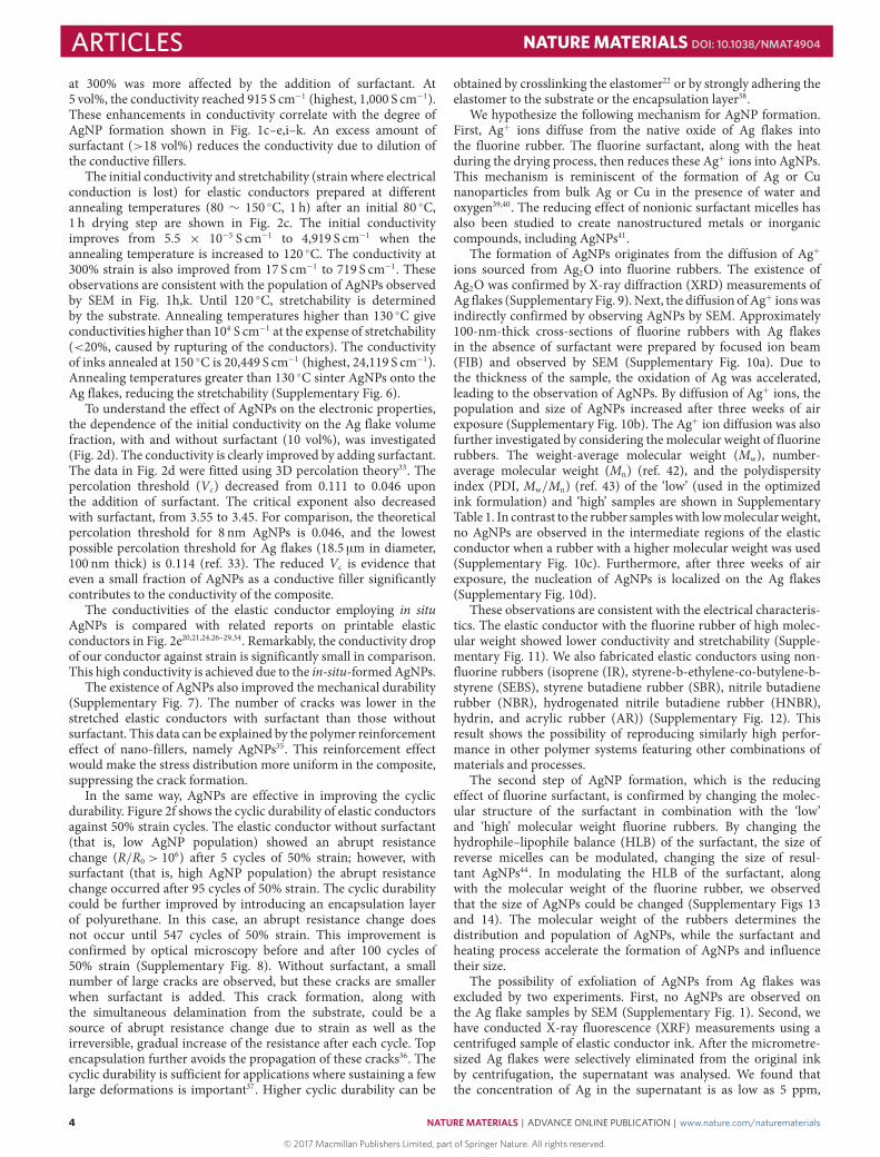
Figure 2 | Electrical characteristics of elastic conductors with di�erent formulations. a, Conductivity–strain characteristics of elastic conductors with andwithout surfactant and with and without high-temperature treatment. b, Dependence of conductivity on the volume fraction of fluorine surfactant.c, Dependence of conductivity and stretchability on the post-process annealing temperature. d, Dependence of conductivity on the volume fraction ofAg flakes, with and without surfactant. Error bars in b–d describe the standard error. e, Comparison of conductivity–strain characteristics with otherprintable elastic conductors. f, Cyclic durability of elastic conductors. Use of surfactant and encapsulation improves the cyclic durability.
reduced in the absence of surfactant or without an additionalheating process. The contribution of AgNPs to the conductivityis confirmed by the conductivity–strain characteristics in Fig. 2a.The elastic conductors with surfactant exhibited a high conductivityof 4,919 S cm−1 without strain and 719 S cm−1 at a strain of 300%.On the other hand, elastic conductors without surfactant show aconductivity of 3,727 S cm−1 and 297 S cm−1 at strains of 0% and300%, respectively. Elastic conductors with surfactant prepared atlow temperature show conductivities of 5.5 × 10⁻⁵ S cm−1 and17 S cm−1 at strains of 0% and 300%, respectively. Thus, surfactantand heating are necessary to generate AgNPs in the elastomer,
leading to high conductivities over a wide range of applied strain.Indeed, the difference in conductivity for elastic conductors withand without surfactant is less than an order of magnitude; however,it will be shown that the selection of the fluorine rubber has a majorinfluence on AgNP formation.
The effects of the surfactant and heating processes on theelectrical performancewere investigated. In Fig. 2b, the conductivityfor various surfactant volume fractions, while keeping the ratio ofother components the same, at 0% and 300% strain is shown. For10 vol% of surfactant, the initial conductivity reached a maximumvalue of 4,972 S cm−1 (highest, 6,168 S cm−1). The conductivity
NATUREMATERIALS | ADVANCE ONLINE PUBLICATION | www.nature.com/naturematerials
© 2017 Macmillan Publishers Limited, part of Springer Nature. All rights reserved.
3
ARTICLES NATUREMATERIALS DOI: 10.1038/NMAT4904
at 300% was more affected by the addition of surfactant. At5 vol%, the conductivity reached 915 S cm−1 (highest, 1,000 S cm−1).These enhancements in conductivity correlate with the degree ofAgNP formation shown in Fig. 1c–e,i–k. An excess amount ofsurfactant (>18 vol%) reduces the conductivity due to dilution ofthe conductive fillers.
The initial conductivity and stretchability (strain where electricalconduction is lost) for elastic conductors prepared at differentannealing temperatures (80 ∼ 150 ◦C, 1 h) after an initial 80 ◦C,1 h drying step are shown in Fig. 2c. The initial conductivityimproves from 5.5 × 10⁻⁵ S cm−1 to 4,919 S cm−1 when theannealing temperature is increased to 120 ◦C. The conductivity at300% strain is also improved from 17 S cm−1 to 719 S cm−1. Theseobservations are consistent with the population of AgNPs observedby SEM in Fig. 1h,k. Until 120 ◦C, stretchability is determinedby the substrate. Annealing temperatures higher than 130 ◦C giveconductivities higher than 104 S cm−1 at the expense of stretchability(<20%, caused by rupturing of the conductors). The conductivityof inks annealed at 150 ◦C is 20,449 S cm−1 (highest, 24,119 S cm−1).Annealing temperatures greater than 130 ◦C sinter AgNPs onto theAg flakes, reducing the stretchability (Supplementary Fig. 6).
To understand the effect of AgNPs on the electronic properties,the dependence of the initial conductivity on the Ag flake volumefraction, with and without surfactant (10 vol%), was investigated(Fig. 2d). The conductivity is clearly improved by adding surfactant.The data in Fig. 2d were fitted using 3D percolation theory33. Thepercolation threshold (Vc) decreased from 0.111 to 0.046 uponthe addition of surfactant. The critical exponent also decreasedwith surfactant, from 3.55 to 3.45. For comparison, the theoreticalpercolation threshold for 8 nm AgNPs is 0.046, and the lowestpossible percolation threshold for Ag flakes (18.5 µm in diameter,100 nm thick) is 0.114 (ref. 33). The reduced Vc is evidence thateven a small fraction of AgNPs as a conductive filler significantlycontributes to the conductivity of the composite.
The conductivities of the elastic conductor employing in situAgNPs is compared with related reports on printable elasticconductors in Fig. 2e20,21,24,26–29,34. Remarkably, the conductivity dropof our conductor against strain is significantly small in comparison.This high conductivity is achieved due to the in-situ-formed AgNPs.
The existence of AgNPs also improved the mechanical durability(Supplementary Fig. 7). The number of cracks was lower in thestretched elastic conductors with surfactant than those withoutsurfactant. This data can be explained by the polymer reinforcementeffect of nano-fillers, namely AgNPs35. This reinforcement effectwould make the stress distribution more uniform in the composite,suppressing the crack formation.
In the same way, AgNPs are effective in improving the cyclicdurability. Figure 2f shows the cyclic durability of elastic conductorsagainst 50% strain cycles. The elastic conductor without surfactant(that is, low AgNP population) showed an abrupt resistancechange (R/R0 > 106) after 5 cycles of 50% strain; however, withsurfactant (that is, high AgNP population) the abrupt resistancechange occurred after 95 cycles of 50% strain. The cyclic durabilitycould be further improved by introducing an encapsulation layerof polyurethane. In this case, an abrupt resistance change doesnot occur until 547 cycles of 50% strain. This improvement isconfirmed by optical microscopy before and after 100 cycles of50% strain (Supplementary Fig. 8). Without surfactant, a smallnumber of large cracks are observed, but these cracks are smallerwhen surfactant is added. This crack formation, along withthe simultaneous delamination from the substrate, could be asource of abrupt resistance change due to strain as well as theirreversible, gradual increase of the resistance after each cycle. Topencapsulation further avoids the propagation of these cracks36. Thecyclic durability is sufficient for applications where sustaining a fewlarge deformations is important37. Higher cyclic durability can be
obtained by crosslinking the elastomer22 or by strongly adhering theelastomer to the substrate or the encapsulation layer38.
We hypothesize the following mechanism for AgNP formation.First, Ag+ ions diffuse from the native oxide of Ag flakes intothe fluorine rubber. The fluorine surfactant, along with the heatduring the drying process, then reduces these Ag+ ions into AgNPs.This mechanism is reminiscent of the formation of Ag or Cunanoparticles from bulk Ag or Cu in the presence of water andoxygen39,40. The reducing effect of nonionic surfactant micelles hasalso been studied to create nanostructured metals or inorganiccompounds, including AgNPs41.
The formation of AgNPs originates from the diffusion of Ag+ions sourced from Ag2O into fluorine rubbers. The existence ofAg2O was confirmed by X-ray diffraction (XRD) measurements ofAg flakes (Supplementary Fig. 9). Next, the diffusion ofAg+ ionswasindirectly confirmed by observing AgNPs by SEM. Approximately100-nm-thick cross-sections of fluorine rubbers with Ag flakesin the absence of surfactant were prepared by focused ion beam(FIB) and observed by SEM (Supplementary Fig. 10a). Due tothe thickness of the sample, the oxidation of Ag was accelerated,leading to the observation of AgNPs. By diffusion of Ag+ ions, thepopulation and size of AgNPs increased after three weeks of airexposure (Supplementary Fig. 10b). The Ag+ ion diffusion was alsofurther investigated by considering the molecular weight of fluorinerubbers. The weight-average molecular weight (Mw), number-average molecular weight (Mn) (ref. 42), and the polydispersityindex (PDI, Mw/Mn) (ref. 43) of the ‘low’ (used in the optimizedink formulation) and ‘high’ samples are shown in SupplementaryTable 1. In contrast to the rubber sampleswith lowmolecularweight,no AgNPs are observed in the intermediate regions of the elasticconductor when a rubber with a higher molecular weight was used(Supplementary Fig. 10c). Furthermore, after three weeks of airexposure, the nucleation of AgNPs is localized on the Ag flakes(Supplementary Fig. 10d).
These observations are consistent with the electrical characteris-tics. The elastic conductor with the fluorine rubber of high molec-ular weight showed lower conductivity and stretchability (Supple-mentary Fig. 11). We also fabricated elastic conductors using non-fluorine rubbers (isoprene (IR), styrene-b-ethylene-co-butylene-b-styrene (SEBS), styrene butadiene rubber (SBR), nitrile butadienerubber (NBR), hydrogenated nitrile butadiene rubber (HNBR),hydrin, and acrylic rubber (AR)) (Supplementary Fig. 12). Thisresult shows the possibility of reproducing similarly high perfor-mance in other polymer systems featuring other combinations ofmaterials and processes.
The second step of AgNP formation, which is the reducingeffect of fluorine surfactant, is confirmed by changing the molec-ular structure of the surfactant in combination with the ‘low’and ‘high’ molecular weight fluorine rubbers. By changing thehydrophile–lipophile balance (HLB) of the surfactant, the size ofreverse micelles can be modulated, changing the size of resul-tant AgNPs44. In modulating the HLB of the surfactant, alongwith the molecular weight of the fluorine rubber, we observedthat the size of AgNPs could be changed (Supplementary Figs 13and 14). The molecular weight of the rubbers determines thedistribution and population of AgNPs, while the surfactant andheating process accelerate the formation of AgNPs and influencetheir size.
The possibility of exfoliation of AgNPs from Ag flakes wasexcluded by two experiments. First, no AgNPs are observed onthe Ag flake samples by SEM (Supplementary Fig. 1). Second, wehave conducted X-ray fluorescence (XRF) measurements using acentrifuged sample of elastic conductor ink. After the micrometre-sized Ag flakes were selectively eliminated from the original inkby centrifugation, the supernatant was analysed. We found thatthe concentration of Ag in the supernatant is as low as 5 ppm,
4
© 2017 Macmillan Publishers Limited, part of Springer Nature. All rights reserved.
NATUREMATERIALS | ADVANCE ONLINE PUBLICATION | www.nature.com/naturematerials

NATUREMATERIALS DOI: 10.1038/NMAT4904 ARTICLESa
c
d
e f
b
Polyurethanesubstrate
Sensor(pressure or temperature)
Rigid resist/polyurethane
Elasticconductor
Sensor (pressure ortemperature)
Rigid resist/polyurethane
Elastic conductor wirings
108
107
106
105
104
103
1 2 3 4 5
Resi
stan
ce (Ω
)
Force (N)
104
105
106
107
108
109
1010
26 28 30 32 34 36 38 40
Resi
stan
ce (Ω
)
Temperature (°C)
Lamination
Ni:silicone composite Graphite:polyacrylatecomposite
∼120% stretched
Figure 3 | Stretchable and fully printed sensor networks for stretchable robotics. a, Structure of sensors. Sensors for pressure or temperature are placedon printed resist and polyurethane islands and wired using elastic conductors. b–d, Picture of sensors laminated on textiles. b, Magnified image of a sensor.Scale bar, 5 mm. c,d, Sensor networks in the unstretched and 120% stretched conditions, respectively. Scale bars, 2 cm. e,f, Performance of printed sensorsfor pressure and temperature, respectively.
which is much less than the expected concentration based on SEMobservation of dried elastic conductors (∼25wt%).
As reported previously, AgNPs have a unique ability to organizeunder external influences30, be it mechanical strain29 or electricalfields31. Through SEM images of the elastic conductor, twointeresting phenomena are observed. From SEM images taken whenthe conductor is stretched, the AgNPs form chains (SupplementaryFig. 15), contributing to the high conductivity at large strain,consistent with a previous report29. When the size of fillers is smallenough to share surrounding polymer chains35, nanoparticles canalso be aligned along with the polymer chains that get aligned bystrain. Additionally, AgNPs start to form nanorods when left inthe atmosphere, both on the surface and inside of the elastomer,regardless of strain (Supplementary Fig. 16)40.
We have confirmed that extraordinarily large conduction reliesprimarily on electrons, not diffused Ag ions. Supplementary Fig. 17shows the frequency dependence of the electrical characteristics.The result shows a flat impedance and constant phase (0◦) from20Hz to 1MHz, clearly indicating that conduction is primarily viaelectrons through Ag flakes and AgNPs. Here we wish to note thathigh-resolution TEM images (Fig. 1l–n) of AgNPs embedded inthe rubber matrix clearly show the formation of a high density ofAgNPs, whose diameters are typically 2–10 nm, with spacings of2–10 nm, which is small enough to ensure tunnelling conduction33.This result strongly supports the high conductivity of our materialsfrom the structural viewpoint. Further structural characterization,and the controlled formation in situ of smaller conducting fillers willprobably lead to even higher conductivity values.
NATUREMATERIALS | ADVANCE ONLINE PUBLICATION | www.nature.com/naturematerials
© 2017 Macmillan Publishers Limited, part of Springer Nature. All rights reserved.
5

ARTICLES NATUREMATERIALS DOI: 10.1038/NMAT4904
Similar performance enhancement can be expected by alsoadding AgNPs in a 1:100wt% ratio with respect to Ag flakes tothe ink (Supplementary Fig. 18). However this approach resulted inlower stretchability (failure at 106%) without surfactant. This couldbe caused by difficulty in dispersing the AgNPs.
To demonstrate the practical feasibility of this elastic conductor,we fabricated fully printed elastic sensor networks. Figure 3a showsthe structure, consisting of pressure and temperature sensors onrigid islands of photoresist and polyurethane, wired using elasticconductors. In this way, the sensing elements can be isolated fromstrain when the whole system is stretched2,20,45. The stretchabilityrequirements for interconnects are normally much larger than thatof the total system46. These fully printed sensors can be easilylaminated onto various stretchable substrates or curved surfaces,giving sensor functions. Here we chose textile substrates (Supple-mentary Fig. 19). Figure 3b–d shows the laminated sensors ontextiles. These devices are still stretchable and functional after lam-ination even when stretched by 120%, the limitation of the chosentextile substrate. The sensor sheet is as large as 30 × 20 cm2. Thesensors can be easily placed on humans or robots by just beingworn. The output of the sensors is transmitted through the elasticconductor wiring.
The detailed sensor performances are shown in Fig. 3e,f. Thepressure sensor is a composite of Ni particles and silicone47,48,which can sense a weak force (1 ∼ 5N). The temperature sensoris a composite of graphite and an acrylic polymer49, which cansense temperatures in the range of 28 ∼ 36 ◦C. This is suitablefor measuring temperatures near body and room temperature. Theresistances of these sensors are much higher than the resistanceof the stretchable conductor, enabling accurate sensing until 250%strain. Strains higher than 275% caused the rupture of the substrateat the interface between the rigid islands and the polyurethanesubstrate (Supplementary Figs 20 and 21).
In our elastic conductors with in-situ-formed AgNPs, extraordi-narily high conductivity has been achieved whilst maintaining highstretchability, although these two properties are in a trade-off. Highconductivity is needed to reduce transmission losses as well as toimprove the frequency response. High stretchability is importantfor wearables and robotics applications. For example, stretchablesensors used in conformable, form-fitting sportswear require upto 200% stretchability for flexible areas such as elbows and knees.Even higher stretchability is necessary for robotics applications suchas stretchable robotic arms used in industry, which are frequentlydesigned to surpass human capabilities.
The fabrication process for the proposed elastic conductors ishighly compatible with large-area and high-throughput printingprocesses. The in situ formation of AgNPs in the elastomermatrix improves the conductivity for two reasons. First, uniformlydispersed AgNPs improve the percolation between micrometre-sized Ag flakes. Second, crack formation is suppressed due to thereinforcement effect of AgNPs. The population and size of AgNPscould be controlled by selection of the Ag flakes, elastomer matrix,and surfactant. This demonstration introduces a new concept tofurther improve elastic conductors. It is expected that the electricaland mechanical performance of these types of composites canbe further improved by investigation of elastomers, surfactants,Ag flakes, and diffused Ag ions. At present, costs are dominatedprimarily by the price of Ag flakes despite the fact that recyclingor extraction of Ag from composites are well-established processes.Replacing Ag flakes with cheaper metals would further reducecosts. Cu flakes are a promising candidate because nanoparticleformation in the presence of bulk Cu has been reported40. Finally,we showed that fully printed sensor networks suitable for complexand dynamic surfaces could be developed. This ushers in newapplications in the field of stretchable electronics, especially inrobotics and deformable electronics37,50.
MethodsMethods, including statements of data availability and anyassociated accession codes and references, are available in theonline version of this paper.
Received 18 November 2016; accepted 7 April 2017;published online 15 May 2017
References1. Kim, J. et al . Stretchable silicon nanoribbon electronics for skin prosthesis.
Nat. Commun. 5, 5747 (2014).2. Kim, D.-H. et al . Epidermal electronics. Science 333, 838–843 (2011).3. Someya, T. et al . A large-area, flexible pressure sensor matrix with organic
field-effect transistors for artificial skin applications. Proc. Natl Acad. Sci. USA101, 9966–9970 (2004).
4. Someya, T. et al . Conformable, flexible, large-area networks of pressure andthermal sensors with organic transistor active matrixes. Proc. Natl Acad. Sci.USA 102, 12321–12325 (2005).
5. Menguc, Y. et al . Wearable soft sensing suit for human gait measurement. Int. J.Rob. Res. 33, 1748–1764 (2014).
6. Tee, B. C.-K. et al . A skin-inspired organic digital mechanoreceptor. Science350, 313–316 (2015).
7. Dickey, M. D. et al . Eutectic gallium–indium (EGaIn): a liquid metal alloy forthe formation of stable structures in microchannels at room temperature.Adv. Funct. Mater. 18, 1097–1104 (2008).
8. Chiechi, R. C., Weiss, E. A., Dickey, M. D. &Whitesides, G. M. Eutecticgallium–indium (EGaIn): a moldable liquid metal for electrical characterizationof self-assembled monolayers. Angew. Chem. Int. Ed. 47, 142–144 (2008).
9. Hirsch, A., Michaud, H. O., Gerratt, A. P., de Mulatier, S. & Lacour, S. P.Intrinsically stretchable biphasic (solid–liquid) thin metal films. Adv. Mater. 28,4507–4512 (2016).
10. Savagatrup, S. et al . Plasticization of PEDOT:PSS by common additives formechanically robust organic solar cells and wearable sensors. Adv. Funct.Mater. 25, 427–436 (2015).
11. Yue, W. et al . A highly stretchable, transparent and conductive polymer.Sci. Adv. 3, e1602076 (2017).
12. Keplinger, C. et al . Stretchable, transparent, ionic conductors. Science 341,984–987 (2013).
13. Xu, S. et al . Stretchable batteries with self-similar serpentine interconnects andintegrated wireless recharging systems. Nat. Commun. 4, 1543 (2013).
14. Gonzalez, M. et al . Design of metal interconnects for stretchable electroniccircuits.Microelectron. Reliab. 48, 825–832 (2008).
15. Vural, M., Behrens, A. M., Ayyub, O. B., Ayoub, J. J. & Kofinas, P. Sprayableelastic conductors based on composites. ACS Nano 9, 336–344 (2015).
16. Park, M. et al . Highly stretchable electric circuits from a compositematerial of silver nanoparticles and elastomeric fibres. Nat. Nanotech. 7,803–809 (2012).
17. Kaltenbrunner, M. et al . An ultra-lightweight design for imperceptible plasticelectronics. Nature 499, 458–463 (2013).
18. Lacour, S. P., Wagner, S., Huang, Z. & Suo, Z. Stretchable gold conductors onelastomeric substrates. Appl. Phys. Lett. 82, 2404–2406 (2003).
19. Minev, I. R. et al . Electronic dura mater for long-term multimodal neuralinterfaces. Science 347, 159–163 (2015).
20. Sekitani, T. et al . Stretchable active-matrix organic light-emitting diode displayusing printable elastic conductors. Nat. Mater. 8, 494–499 (2009).
21. Chun, K. et al . Highly conductive, printable and stretchable composite films ofcarbon nanotubes and silver. Nat. Nanotech. 5, 853–857 (2010).
22. Sekitani, T. et al . A rubberlike stretchable active matrix using elasticconductors. Science 321, 1468–1472 (2008).
23. Lipomi, D. J. et al . Skin-like pressure and strain sensors based on transparentelastic films of carbon nanotubes. Nat. Nanotech. 6, 788–792 (2011).
24. Liang, J., Tong, K. & Pei, Q. A water-based silver-nanowire screen-print ink forthe fabrication of stretchable conductors and wearable thin-film transistors.Adv. Mater. 28, 5986–5996 (2016).
25. Tybrandt, K. & Vörös, J. Fast and efficient fabrication of intrinsically stretchablemultilayer circuit boards by wax pattern assisted filtration. Small 12,180–184 (2016).
26. Araki, T., Nogi, M., Suganuma, K., Kogure, M. & Kirihara, O. Printable andstretchable conductive wirings comprising silver flakes and elastomers.IEEE Electron Device Lett. 32, 1424–1426 (2011).
27. Matsuhisa, N. et al . Printable elastic conductors with a high conductivity forelectronic textile applications. Nat. Commun. 6, 7461 (2015).
28. Ma, R., Kang, B., Cho, S., Choi, M. & Baik, S. Extraordinarily high conductivityof stretchable fibers of polyurethane and silver nanoflowers. ACS Nano 9,10876–10886 (2015).
6
© 2017 Macmillan Publishers Limited, part of Springer Nature. All rights reserved.
NATUREMATERIALS | ADVANCE ONLINE PUBLICATION | www.nature.com/naturematerials

NATUREMATERIALS DOI: 10.1038/NMAT4904 ARTICLES29. Kim, Y. et al . Stretchable nanoparticle conductors with self-organized
conductive pathways. Nature 500, 59–63 (2013).30. Balazs, A. C., Emrick, T. & Russell, T. P. Nanoparticle polymer composites:
where two small worlds meet. Science 314, 1107–1110 (2006).31. Koshi, T. & Iwase, E. Self-healing metal wire using electric field trapping of
metal nanoparticles. Jpn. J. Appl. Phys. 54, 06FP03 (2015).32. Wang, C. et al . Significance of the double-layer capacitor effect in polar
rubbery dielectrics and exceptionally stable low-voltage high transconductanceorganic transistors. Sci. Rep. 5, 17849 (2015).
33. Li, J. & Kim, J.-K. Percolation threshold of conducting polymer compositescontaining 3D randomly distributed graphite nanoplatelets. Compos. Sci.Technol. 67, 2114–2120 (2007).
34. Stoyanov, H., Kollosche, M., Risse, S., Waché, R. & Kofod, G. Soft conductiveelastomer materials for stretchable electronics and voltage controlled artificialmuscles. Adv. Mater. 25, 578–583 (2013).
35. Allegra, G., Raos, G. & Vacatello, M. Theories and simulations ofpolymer-based nanocomposites: from chain statistics to reinforcement.Prog. Polym. Sci. 33, 683–731 (2008).
36. Sawyer, E. J. et al . Large increase in stretchability of organic electronic materialsby encapsulation. Extreme Mech. Lett. 8, 78–87 (2016).
37. Vanfleteren, J. et al . Arbitrarily shaped 2.5D circuits using stretchableinterconnections and embedding in thermoplastic polymers. Procedia Technol.15, 208–215 (2014).
38. Li, C.-Y. & Liao, Y.-C. Adhesive stretchable printed conductive thin filmpatterns on PDMS surface with an atmospheric plasma treatment. ACS Appl.Mater. Interfaces 8, 11868–11874 (2016).
39. Rybak, B. M., Ornatska, M., Bergman, K. N., Genson, K. L. & Tsukruk, V. V.Formation of silver nanoparticles at the air–water interface mediated by amonolayer of functionalized hyperbranched molecules. Langmuir 22,1027–1037 (2006).
40. Glover, R. D., Miller, J. M. & Hutchison, J. E. Generation of metal nanoparticlesfrom silver and copper objects: nanoparticle dynamics on surfaces andpotential sources of nanoparticles in the environment. ACS Nano 5,8950–8957 (2011).
41. Lee, M.-H., Oh, S.-G., Suh, K.-D., Kim, D.-G. & Sohn, D. Preparation of silvernanoparticles in hexagonal phase formed by nonionic Triton X-100 surfactant.Colloids Surf. A 210, 49–60 (2002).
42. Fried, J. R. Polymer Science and Technology (Prentice Hall, 2003).43. Stepto, R. F. T. Dispersity in polymer science (IUPAC Recommendations 2009).
Pure Appl. Chem. 81, 351–353 (2009).44. Petit, C., Lixon, P. & Pileni, M. P. In situ synthesis of silver nanocluster in AOT
reverse micelles. J. Phys. Chem. 97, 12974–12983 (1993).45. Wagner, S. et al . Electronic skin: architecture and components. Physica E 25,
326–334 (2004).
46. Zhang, Y. et al . Experimental and theoretical studies of serpentinemicrostructures bonded to prestrained elastomers for stretchable electronics.Adv. Funct. Mater. 24, 2028–2037 (2014).
47. Canavese, G., Lombardi, M., Stassi, S. & Pirri, C. F. Comprehensivecharacterization of large piezoresistive variation of Ni-PDMS composites.Appl. Mech. Mater. 110–116, 1336–1344 (2011).
48. Stassi, S. & Canavese, G. Spiky nanostructured metal particles as filler ofpolymeric composites showing tunable electrical conductivity. J. Polym. Sci. 50,984–992 (2012).
49. Yokota, T. et al . Ultraflexible, large-area, physiological temperature sensors formultipoint measurements. Proc. Natl Acad. Sci. USA 112, 14533–14538 (2015).
50. Wehner, M. et al . An integrated design and fabrication strategy for entirely soft,autonomous robots. Nature 536, 451–455 (2016).
AcknowledgementsThis work was financially supported by the JST ERATO Bio-Harmonized ElectronicsProject. The authors appreciate T. Kikitsu and Y. Maebashi at the MaterialsCharacterization Support Unit, CEMS, RIKEN for discussions on the observation of Agnanoparticles. The authors also acknowledge Y. Jimbo, A. Miyamoto, M. Mori andK. Okaniwa at the University of Tokyo for discussions regarding the fabrication processesof printed stretchable sensors, and T. Sekitani at Osaka University for discussions on thedesign of elastic conductors. The authors would also like to express their gratitude toD. Ordinario, S. Lee and H. Jinno at University of Tokyo, S. Park and X. Xu at RIKEN,and M. Kaltenbrunner at Johannes Kepler University Linz for helpful discussions. Theauthors are grateful to Daikin Industries for gifting the fluorine rubbers used in thiswork, along with Yasushi Sano (S-P Solutions) and Goo Chemicals for providing theprintable rigid resist. The SEM images were obtained at the shared facilities at RIKEN.N.M. is supported by Advanced Leading Graduate Course for Photon Science (ALPS)and the Japan Society for the Promotion of Science (JSPS) research fellowship for youngscientists. H.J. is supported by Graduate Program for Leaders in Life Innovation (GPLLI).
Author contributionsN.M., H.J. and T.Y. fabricated materials and devices. N.M., D.I., T.Y. and D.H.characterized elastic conductors. N.M., D.I., Y.M., A.I., P.Z. and D.H. analysed the data.N.M., H.J., Y.M., A.I. and T.S. designed materials. N.M., H.J., P.Z. and T.S. wrotemanuscript. T.S. supervised this project.
Additional informationSupplementary information is available in the online version of the paper. Reprints andpermissions information is available online at www.nature.com/reprints. Publisher’s note:Springer Nature remains neutral with regard to jurisdictional claims in published mapsand institutional affiliations. Correspondence and requests for materials should beaddressed to T.S.
Competing financial interestsThe authors declare no competing financial interests.
NATUREMATERIALS | ADVANCE ONLINE PUBLICATION | www.nature.com/naturematerials
© 2017 Macmillan Publishers Limited, part of Springer Nature. All rights reserved.
7

ARTICLES NATUREMATERIALS DOI: 10.1038/NMAT4904
MethodsInk preparation and printing. Ag flakes (product number: 327077 Aldrich, Agflakes, 10 µm,>99.9% trace metals basis, Sigma Aldrich), fluorine rubbers (lowmolecular weight, DAI-EL G8001; high molecular weight, DAI-EL G801; liquidfluorine rubber, G101, Daikin Industries), fluorine surfactant (S-386 (HLB: 12.6),AGC Chemical; FC4430 (HLB: 15.1), 3M, USA; FC4432 (HLB: 11.3), 3M, USA)and MIBK were mixed with a magnetic stirrer for 12 h in a weight ratio of 3:1:0.1:1.The ink was then printed on a 20-µm-thick polyurethane substrate (NSKEchomark) through a shadow mask made of a 125-µm-thick polyimide film(UPILEX-125S, UBE Industries), followed by drying at 80 ◦C for 1 h and 120 ◦C for1 h in an oven (DKN-302, Yamato Scientific). The stretchability of the substrate istypically between 300 and 400%. For comparison, elastic conductors werefabricated using the following non-fluorine rubbers: IR (IR 2200, ZEON), SEBS(N504, Asahi-Kasei Chemicals), SBR (Nipol 1502, ZEON), HNBR (Zetpol 2000L,ZEON), hydrin (Hydrin C2000L, ZEON), AR (AR 12, ZEON) and NBR (Nipol1042, ZEON). The ink formulation was set to ensure that the volume fraction of Agflakes in elastomer was the same (Ag flakes: elastomers: solvent= 13.7: 26.4: 59.9 involume, drying process: 80 ◦C for 1 h). For control experiments, elastic conductorswere fabricated by adding AgNPs in a 1:100wt% ratio to Ag flakes (∼20 nmNP-AG-7-5, EM Japan), or by replacing Ag flakes with AgNPs (∼20 nm, Ag202,Shoei Chemical). The ink formulation and drying condition were fixed to theoptimized ink (Ag flakes or AgNPs : fluorine rubber (low molecular weight):surfactant (S-386): MIBK= 3:1:0.1:1, drying condition: 80 ◦C for 1 h and 120 ◦Cfor 1 h).
Electrical evaluation of elastic conductor. Elastic conductors were printed with awidth of 0.5mm. Thicknesses were measured by a profilometer (Dektak XT,BRUKER). The average thickness was approximately 30 µm, which is determinedby the ink formulation and thickness of stencil masks. The resistance was thenmeasured using the four-point probe method and a digital multimeter (34410A,Agilent). The distance between measuring electrodes was set to be 30mm, which isthe initial length. The elastic conductor was stretched by a high-precisionmechanical system (AG-X, Shimadzu). At least five traces were tested for eachcondition. The conductivity was calculated using the initial geometry andresistance. The conductivity during stretching was calculated under the assumptionthat the total volume does not change. The frequency dependence of the elasticconductors was measured with the above-mentioned device geometry using aprecision LCR meter (4284A, Agilent).
3D percolation theory and theoretical percolation threshold. The equation for3D percolation theory is described in equation (1) (ref. 33), where σ and σ0 denotethe conductivity of the elastic conductor and the bulk Ag, respectively. Vf, Vc and sare the volume fraction of Ag, percolation threshold, and exponent factor,respectively. Here the bulk Ag conductivity (σ0) is set to 8.5× 10⁵ S cm−1. Thevalues of Vc and s are obtained by fitting the experimental data for elasticconductors with and without surfactant. The theoretical percolation threshold forAg flakes and nanoparticles are obtained by equations (2) and (3) (ref. 33),respectively. D, t , DIP, and d are the diameter of Ag flakes, thickness of Ag flakes,tunnelling distance, and diameter of Ag nanoparticles, respectively. Here valuesof 18.5 µm, 0.1 µm, 10 nm (ref. 33), and 8 nm are applied to D, t , DIP, andd , respectively.
σ =σ0 (Vf−Vc)s (1)
Vc_flakes=27πD2t
4(D+DIP)3 (2)
Vc_sphere=πd3
6(d+DIP)3 (3)
SEM and TEM observation. The surface and cross-sectional SEM images weretaken using an S4800 (Hitachi High Technologies) with an acceleration voltage of3 kV. The cross-section was obtained by cutting with a sharp razor blade whilesamples were cooled in liquid nitrogen. Thin samples (approximately 100 nm) wereprepared by an FIB-SEM (NB5000, Hitachi High Technologies). Surface-etched
samples were prepared by Ar ion beam milling (RES100, Baltec). The conditionwas set to very mild to avoid damage to the samples (acceleration voltage andcurrent: 3 kV, 1mA, beam angle: 3◦, sample holder tilt angle: 35◦, oscillation angle:20◦, process time: 4 h). The samples processed with an FIB-SEM or Ar ion beammilling were observed by SEM (JSM6330F, JEOL) with an acceleration voltage of3 kV. TEM images of samples processed with an FIB were obtained by a JEM-2100F(JEOL) with an acceleration voltage of 200 kV.
XRD and XRF analysis. An out-of-plane XRD spectra of Ag flakes were obtainedusing a Rigaku SmartLab with a Cu-Kα source (λ=1.541Å) at 40 kV and 30mA.The scan rate was 0.2◦ s−1 and the measurement step was set to 0.02◦ in a 2θ–θconfiguration. XRF analysis was carried out on the centrifuged ink using a RigakuEDXL300. The analysed ink was prepared by centrifuging an elastic conductor ink(Ag flakes: low molecular weight fluorine rubber: fluorine surfactant (S-386),MIBK= 3:1:0.1:1 in weight) using Kubota 3740 at 10,000 r.p.m. for 10min, andfiltering the supernatant through a polytetrafluoroethylene (PTFE) filter with a200 nm pore size.
Pressure sensing ink or temperature sensing ink. The pressure sensitive ink wasbased on a previously reported Ni-microparticle and silicone composite47,48. Thedeformation of this Ni-microparticle and silicone composite decreases the distancebetween conducting particles, lowering the resistance. Ni microparticles (NickelPowder Type 123, Nikko Rica) and silicone prepolymer (Silpot 184, Toray DowCorning) were mixed using a planetary centrifugal mixer (ARV-310, Thinky) at2,000 r.p.m. for 5min under vacuum. Then, the curing agent was added to theblend and mixed again at 2,000 r.p.m. for 5min under vacuum. The mixture weightratio was Ni microparticles: silicone prepolymer: curing agent= 38.5:10:1. Themixture was then printed using a 375 µm polyimide shadow mask and cured at60 ◦C for 6 h. Temperature sensing ink was based on our previous report49. Thecomposite consists of graphite and a semi-crystalline acrylate copolymer(graphite:polymer, 1:3 wt). Under heating, thermal expansion of the polymerisolates graphite flakes and increases the resistance. The polymer was synthesizedfrom 75wt% of octadecyl acrylate and 25wt% of butyl acrylate. The ink wasprinted through a 25 µm polyimide mask. The ink and squeegee were heated at80 ◦C in advance to melt the ink. The sensitivity range can be tuned precisely from15 to 50 ◦C by modifying the acrylic polymer structure49.
Stretchable pressure and temperature sensor. The schematics of the sensor areavailable in Fig. 3a. An ultraviolet(UV)-curable rigid resist (PSR-310A, GooChemical) was printed on a polyurethane substrate that had been treated withUV–ozone (UV-1, SAMCO) to create rigid islands using a 75-µm-thick polyimideshadow mask. The ink was then cured for 10min using a UV lamp box(BOX-W10D, Sunhayato). The substrate was again treated by UV–ozone toimprove the adhesion with subsequent layers. A water-based polyurethane ink(Aqua-PEX, MINO Group) was printed with a 125 µm polyimide shadow mask tosuppress the stress concentration at the rigid–stretchable interface by making agradual transition of stretchability. Printed patterns were dried and cured at 80 ◦Cfor 1 h in an oven, resulting in a thickness of 50 µm. Then, elastic conductor wiringsand pressure/temperature sensors were formed using the above-mentionedmethods. For device evaluation, the resistance was measured using a digitalmultimeter (34410A, Agilent) while applying pressure or temperature. Thepressure and temperature was applied using a forcemeter (FGP-1, SHIMPO) anda low-temperature thermostatic water bath (TRL-11LP, Thomas), respectively.The pressure sensor was evaluated while strain was applied, as shown inSupplementary Fig. 20.
Textile-based stretchable sensor. Stretchable sensors were first fabricated on apolyurethane film as above mentioned. The device was then laminated onto atextile substrate using the following methods (Supplementary Fig. 19). Athermoplastic polyurethane sheet (NSK Echomark) was laminated onto the textileat 120 ◦C for 5min using a pressure of 30 kPa. The sensors were then laminated onthem at 120 ◦C for 10 s using a pressure of 30 kPa. Finally, another thermoplasticpolyurethane sheet was laminated as an encapsulation layer.
Data availability. The data that support the findings of this study are availablefrom the corresponding author upon request.
© 2017 Macmillan Publishers Limited, part of Springer Nature. All rights reserved.
NATUREMATERIALS | www.nature.com/naturematerials