printed circuit board layout for linear switching amplifiers · printed circuit board layout for...
TRANSCRIPT

www.apexanalog.com© Apex Microtechnology Inc
All rights reserved
Printed Circuit Board Layout for Linea
AN54
r Switching Amplifiers
SECTION I: PURPOSE
The purpose of this application note is to provide engineering development teams with a series of bestpractices to use in designing printed circuit boards (PCB) for the evaluation of power linear and switchingamplifiers. If five people are polled about the proper techniques for laying out such a circuit board, theremight be as many as ten opinions. When taken into consideration, most concerns do actually matter; with theunknown factor being how significant is their contribution. An engineer knows that on some level, all parasit‐ics impress upon a circuit. With that said, this application note is written to facilitate cohesiveness betweenthe engineers working on the project. When viewed from a team perspective, the race to the end can be bet‐ter controlled to result in fewer changes, a reduction in errors, a reduction in cost, and the removal of theneed to debug or to re‐spin. This in turn reduces time to market. It is key to remember just how often theexisting intellectual property can be re‐used and instantiated into the next generation design. A successfuldesign saves money now and also saves money down the road. If this methodology is adopted, it will help toensure success and increase the design team’s effectiveness and productivity.
Best case practices of a layout cannot be discussed without consideration of the progression of the PCB’sdesign. Ideal practices can be put in place to mitigate error and alleviate time lost to debugging. This processbegins before schematic capture and originates with the concept of the circuit. This circuit is intended to be asolution to a challenge generally revolving around some sort of power conversion, some sort of control cir‐cuitry, and some sort of communication. When engineering a circuit solution, the engineer must weigh idealversus practical considerations. With the identification of a practical solution, the engineer begins to identifythe concessions that bound the application. The focus of this document will be to explore a specific set ofconcerns and how a proper layout can help to control, and positively influence, key parameters of a design.The layout can help ensure proper operation and stability of the circuit. Furthermore, proper considerationcan help to ensure the circuit is able to survive sustained usage. The layout must take into account themechanical and thermal stresses caused by the electrical circuit and the respective components. Under cer‐tain conditions a completely acceptable design can self‐destruct, and as such, the manufacturability of thePCB should remain in the back of the circuit designer’s mind. In addition, the designer must always be con‐cerned with noise, whether it is radiated from within the circuitry or conducted. If this school of thought isaccepted and time is taken to implement certain layout principles, the result will be a consistent savings oftime and money, while expertly engineering a robust design.
Most application notes briefly touch on the design of the circuit and its chain of custody. Ideally, a singleelectrical engineer (EE) would develop the circuit and generate the layout. There is no need to highlight theabsurdity of that statement. In actuality, the circuit design is done by an EE (whether the EE be digital, analog,systems, or applications engineer) and then reviewed by colleagues, usually resulting in hasty additions. ThePCB designer then takes their cue from the EE and begins the layout. Down the road the EE makes some editsor fails to tell the PCB designer some piece of information and but now the designer has already done theplacement and routing. This forces a component push and trace to be bumped. Some say this is just the wayit goes, but this is not accurate. The back and forth, and the unintended consequences of the push and bumpmethod, can be removed with the implementation of some specific procedures. This aids in synergy and cre‐ates cohesion within the team. A design is not a hot potato. It should be a baton. This document is brokeninto several sections: the big picture, the schematic capture and the layout itself.
. Apr 2016AN54U Rev A

AN54
SECTION II: THE BIG PICTURE
The “big picture” can be described as a list of specific concerns that should be understood by the teamwhen engineering a solution. This requires an understanding of the discrete components being used; the tol‐erances of the passives; and what takes place period by period. It is critical to determine what takes placeinstantaneously and during crossover, transitioning or switching cycles. The identification of the high currentpaths and what components are in the on‐state is paramount. The DC operating points are not trivial; manydesigns have been degraded due to an oversight of DC performance. The voltage ratings must be identified,in addition to the nominal current, the peak current and power dissipation. A common practice is to set thecurrent limit to 120% of nominal. The limit will vary over temperature. The following is a series of recom‐mended Best Practices.
BEST PRACTICE: IDENTIFY THE HIGH CURRENT PATHS AND LOOPS
The MOSFETs, BJTs and diodes are easily identifiable. From this point, the high current paths can be iden‐tified. These are transitioning loops that need to be minimized. It is important to identify the duty cycles/peri‐ods and to understand the on time and the off time. Take care to understand the effects of parasiticinductance on these paths.
Figure 1:
RCLV-
CC2
V+CC1
VOPA
CComp
19
CC1 CC2
6.8pF
17
ILIM
ILIM15
12
21
5
7
Rbias
U1
PA441
V-
V+
Rg
1 k
Rbal
1 k
minus
plus
D5
D6
Cf
Rf
DNP
100 k
Thermal Pad
32
1 3D1
1
Rgt
0
3
1Gate t
4
RCL+
RCL+
1
2
RCL-
RCL-
13
D2 3
1
Q2
QB
QT
Vout
C722μF
C822μF
V+
C922μF
C1022μF
V-
4
-input
Rload
Vout
100Vrms @ 5A
VO
VO-
Q1
Gate b0
Rgb
FB
2 AN54U Rev A

AN54
BEST PRACTICE: BE DELIBERATE IN CHOOSING THE CAPACITORS FOR THE DESIGN
These selections are frequency dependent/layout sensitive and the said value is never its true value. Takethe time to choose the capacitor based on the electrical function it will support.
With the increasing voltage range of surface mount ceramic capacitors (7kV), high quality ceramic can beused to decrease the distance of the compensation capacitor to the pins.
BEST PRACTICE: RESISTORS ARE A SOURCE OF ERROR, NOISE AND LOSSES
Some resistors matter and some are just resistors. Over time, an understanding of which resistors trulymatter will develop. For example, is it a current sense or a current limit resistor? Is it a resistor that sets a fre‐quency or sets a clock? Is it simply a divider? Each resistor has its own characteristics.
Figure 2:
Use electrolytic to supply charge, Use ceramic for filtering
Compensation should be high quality and rated for the entire differential supply voltage
Figure 3: Axial Versus SMT
Current Sense, Moisture Resistant, Non-Inductive, Non-Magnetic
AEC-Q, Current Sense, Moisture Resistant, Pulse Withstanding, Low Inductance
V+
150V @ 5A
Power Return
-150V @ 5A
+
+ C310μF
C40.1μF
C20.1μF
C110μF
J1
J2
J3
J4
V-
PGNDRCLV-
CC2
V+CC1
CComp
9
6.8pF
8
ILIM
7
5
10
1
2
U1PA441DW
V+
6
AN54U Rev A 3

AN54
BEST PRACTICE:IDENTIFY THE NOISY SIGNALS IN THE CIRCUIT
Identify switching noise, radiated noise and high power returns. It is imperative to identify the on timeand off time of the transistors. Locate the gates, the clock and the digital signals. Once complete, the nextstep in the design process is the placement of the components. This can be a source of many errors andshould be done methodically. If a component is added during a design review, take the time to add and edit,do not just cram, bump and push the part in a negligent fashion. At this point, be certain time has been takento identify the high current loops and the high speed transitions. The high current loops are the critical nodesthat must be engineered to be low impedance. A semi‐copper trace is an impedance that is fluctuating (con‐sider thermal expansion). Take time to get familiar with current density theory and its geometrical determin‐istic property. Let us discuss the benefit of low resistive planes/pours. The routing and placement of thecapacitor can destroy the benefit of its usage. Length increases resistance while an expanded cross sectionwill diminish resistance. As the magnetic field around a conductor fluctuates, so does the induced voltage onthe signal. The one sure way to combat inductance is to shorten the trace.
BEST PRACTICE: ENSURE THE PCB IS MANUFACTURED TO WITHSTAND SUSTAINED TESTING ANDUSAGE
The engineer must consider the stack up and the manufacturability of the design. Consider the pick andplace machine. Think of the board flex. Will there be a need for strain relief due to cabling? Take the time toconsider heat sinking and stand offs. Be meticulous and think about re‐work and testing. Take the time todefine the stack up. What is the copper weight/thickness? What are the minimum and maximum via sizes?What layers are the power planes? What layers are the solid returns or the quiet signal grounds? What layerwill I be routing on? Take some time to learn about copper and its weight/thickness. What is the expectedefficiency of the design? Where are the losses? What is the ambient temperature? What are the minimumand the maximum trace widths? What is the spacing for the weight/thickness chosen?
BEST PRACTICE: OPTIMIZE THE STACK UP FOR SHIELDING AND HEAT SINKING
L1 Power Plane and High Power ComponentsL2 Power Planes repeated (thermal consideration)L3 Solid ground (shielding to protect small signals)L4 Small signal components and sensitive traces
V Ldidt-----= 1V 5nH
2A10ns------------=
4 AN54U Rev A

AN54
Figure 4:
BEST PRACTICE:DO NOT FORGET CIRCUIT PROTECTION, ADD EXTRA LAND PATTERNS
Is a series diode needed? Perhaps a 3.3ohm for input protection for the semiconductors? Does the circuitneed a snubber? Whether for input, flyback, or switching spikes? Add a gate resistor and maybe a diode tohelp turn off the MOSFETs. Is the amplifier adequately protected? Is the current limit resistor Kelvin sense?Does it need a noise filter?
Figure 5:
Input Protection Snubber Flyback Suppression Enhanced Turnoff
3
V+
DX
Rin
3.3
1
4
ON/
BP
VIN
UX
Rsn
10
V-
V+
Csn
0.01μF
PA75
GND
UX
GND
DX
LX
1μH13
DX3
1
10
RX
2
QX
AN54U Rev A 5

AN54
SECTION III SCHEMATIC CAPTURE
Some designs are complex and some can be created in the mind. The scope of this article is intended forcomplex designs. Take for example the need to excite a transducer, move a motor or to convert AC to DC orDC to DC. The origin of the design is the need to provide a company with a solution. Many times this startswith a previous design and migrates to latest and greatest. A design should start in MATLab, Excel or Math‐Cad. The calculations are usually done in conjunction with reading of the data sheet. Once the correct valueshave been calculated it is time for a simulation. During simulation it is time to start thinking about how todebug the circuit board.
BEST PRACTICE: DO I HAVE ALL THE HOOKS IN PLACE TO PROBE?
BEST PRACTICE: MAKE TIME TO READ THE PRODUCT DATA SHEET
This is where the majority of errors can be caught. “There is never time to do it right,but there is time to do it twice.”
BEST PRACTICE:TAKE TIME TO SIMULATE THE DESIGN.
The schematic is a visual representation of a printed circuit board; therefore, it should represent the cir‐cuit board. Be certain to think through the flow of signal connections. It is good practice to use a top page forthe block level diagram. When designing a system, the ability to clearly see the solution is far more importantthan how many pages it covers.
BEST PRACTICE:BEGIN WORKING LEFT TO RIGHT
This is an industry standard. Control the flow of the schematic inputs and outputs. The schematic pageenables all who view it to understand the function of the circuit. The details need to be easily viewed andunderstood. As any engineer knows, the schematic may be used to debug the PCB or to repair the boardmonths or years later. The bill of materials (BOM) is a generated output that can wreak tremendous havocwith the efficiency and effectiveness of the design. Some designs will utilize variants. So it is important to uti‐lize the tools provided by the software. This will ensure the correct instance of the design is populated andworks correctly.
BEST PRACTICE: THE BOM IS GENERATED BY THE SCHEMATIC.
Do not use the common practice of slapping down components as place holders and calculating themlater. All values should be calculated in the design of the circuit/solution using Excel, MATLAB or Mathcad. A
Figure 6:
Rail to Rail Protection Input Protection Kelvin Sense
LX
1μH
V-
V+
UXPA93
DXMURS160-13-F
MURS160-13-FDX
V-
V+ UX
PA98 10DXDX
RCL V-V+
KS+ KS-
6 AN54U Rev A

AN54
perfectly generated BOM will also save time. It is the engineer’s responsibility to ensure the PCB is assembledcorrectly. Pay now or pay later. Either way it will take time – time to configure the bill of materials or time todebug a board.
Figure 7:
For Example: VIN, VOUT, Frequency, IOUT, Current limit, Pulse duration, power, soft start, UVLO, OVLO, ENABLE
BEST PRACTICE: AN ENGINEER SHOULD BE ABLE TO LOOK AT A SCHEMATIC AND KNOW EXACTLYWHAT SIGNALS ARE BEING APPLIED AND EXPECTED
When placing components on the schematic, ensure the proximity is in relation to their importance. Takethe time to read the PCB data sheet. A well written data sheet will highlight critical components. This is one ofthe areas were the data sheet highlights potential mistakes. Also, experience will teach the engineer whatcomponents truly matter. Design reviews can inhibit the need to re‐spin a board due to an oversight. The ideais to assign hierarchy to components and their location to its parent component. Every component does notneed to be right up against the device. For example, here are two extremes: the compensation capacitor ver‐sus an enable divider. When wiring these components, label the nets. This will enable the PCB designer toknow exactly which components are paramount when doing the placement. This is the time to adjust thethickness of the wire on the schematic. It’s as simple as a right click. This will enable all who look at the wireto know to widen the trace. This is also another good place to insert text to show for example “5Vout @ 20A.”Now it is clear this will be a copper pour. Also, when labeling nets, the digital signal paths illuminate them‐selves to the PCB designer. Now the PCB designer will have to identify a digital signal portion of the printedcircuit board.
BEST PRACTICE: CREATE A SECTION OF THE PCB FOR ALL DIGITAL SIGNALS TO ENSURE AN INPUTDO NOT CROSS AN OUTPUT, DO NOT RUN A CLOCKING TRACE OVER A HIGH IMPEDANCE NODE
As was mentioned earlier, when wiring the schematic, it is important to note the loops. If the wire size isadjusted to indicate the current carrying loops, the small signal components are now easily discernible to thePCB designer. This will also help to determine the stack up. How many planes does this design need? Whatareas need to be shielded, mimicked? Which areas require thermal relief? Asking and answering these criticalquestions will ensure the PCB can survive sustained usage.
Clearly identify the return paths by using the ground symbols respective to their identities. Use the threesymbols and explicitly tie them together in an exact location. Do not leave it up to the convenience or the
5 4 3 2
-input J51
1 VRMS @ 100 kHz
V+
150V @ 5A
Power Return
-150V @ 5A
+
+ C310μF
C60.1μF
C50.1μF
C147μF
V+
RTN+
RTN-
V-
V-
+ C410μFD4
160V12
+ C210μFD3
160V12
PGND SGND
Tie Power & Signal Return on Layer 3Net Tie
RCLV-
CC2
V+CC1
VOPA
CComp
19
CC1 CC2
6.8pF
17
ILIM
ILIM15
12
21
5
7
Rbias
U1
PA441
V-
V+
Rg
1 k
Rbal
1 k
minus
plus
D5
D6
Cf
Rf
DNP
100 k
Thermal Pad
32
1 3D1
1
Rgt
0
3
1Gate t
4
RCL+
RCL+
1
2
RCL-
RCL-
13
D2 3
1
Q2
QB
QT
Vout
C722μF
C822μF
V+
C922μF
C1022μF
V-
4
-input
Rload
Vout
100Vrms @ 5A
VO
VO-
Q1
Gate b0
Rgb
FB
Place Diodes and Bypass Capacitors at the DUT Pins
AN54U Rev A 7

AN54
polygon/plane tool. Some tools allow the selection of a location for a short. This is a convenient way to tieanalog and power ground together. Exceptions can be made for a short in a specific location of the chosenlayer. Another trick is to tie the grounds together last, this will ensure control and fidelity of the signals. Assimple as this sounds, this is the one step where the majority of the grief can be eradicated.
Figure 8:
As stated previously, care must be taken to ensure the return paths are separated. But why? First defineground as the return path. Also define the return path as a reference point. This reference point has animpedance; therefore, with current flowing, a voltage drop is created. This is another simple concept thatwreaks havoc with circuitry. So by separating high current returns from the small signal return, less noise andvariation is introduced into the design. This leaves the digital return path. The idea is to separate fast digitalswitching from the small signal circuitry. These high speed clocking signals can couple and induce spikes ontoadjacent signals.
Figure 9:
BEST PRACTICE: USE THE RETURN SYMBOLS TO ENSURE ALL COMPONENTS HAVE THE CORRECTRETURN SYMBOL AND ARE CONNECTED BY DESIGN WITH DELIBERATE FORETHOUGHT ANDINTENTION
There is one step between the schematic capture and the printed circuit board layout. Each design is dif‐ferent, but many times the design rules are the same. The design rules must be considered early in the sche‐matic conception. Many items concerning the physical properties of the board should be conceptualizedduring the schematic capture.
PGND SGND DGND
Tie Power, Signal, & Digital Returns on L3
RCLV-
CC2
V+CC1
VOPA
CComp
19
CC1 CC2
6.8pF
17ILIM
ILIM15
1221
5
7
U1
PA441
V-
V+
Rg
1 k
Rbal
1 k
minus
plus
D5
D6
Cf
Rf
DNP
100 k
-input
5 4 3 2
-input J51
1 VRMS @ 100 kHz
V+
150V @ 5A
Power Return
-150V @ 5A
+
+ C310μF
C60.1μF
C50.1μF
C147μF
V+
RTN+
RTN-
V-
V-
+ C410μFD4
160V12
+ C210μFD3
160V12
PGND SGND
Tie Power & Signal Return on Layer 3Net Tie
8 AN54U Rev A

AN54
BEST PRACTICE: TAKE THE TIME TO SET UP DESIGN RULES AND USE THEM
Save all design rules to a file. This will allow the rapid import of rules for specific cases. Many times theseitems are not considered until late into the design process. When left to the last minute, this will force thecomponents to be pushed and bumped to meet fabrication rules. Use the schematic as a blueprint for properrouting. Use the top level sheet to indicate the stack up. Use text to indicate the critical trace route. Use theschematic features to create rules for trace width. This is the time to be using trace width calculator tools.High voltage solutions require special attention to conductor spacing, trace width, isolation, creepage, andclearance. If unfamiliar with flashover or tracking, now is the time to read about it. Even when defining lowvoltage and low current designs rules, ensure the minimum space is clearly defined. This is usually defined bythe solution density and copper weight/thickness of the printed circuit board. This in turn defines the cost ofthe board.
BEST PRACTICE: PROTECT NOISE SENSITIVE TRACES
Ensure noise sensitive traces are routed away from noisy components and signals. Some examples aresense lines and feedback traces. Take the time to model schematic symbols to allow for Kelvin sensing of cur‐rent limit circuitry.
BEST PRACTICE: USE A DIFFERENTIAL PAIR TOOL
Indicate the following signals as differential pair high speed signals (plus and minus), current limit Kelvinsense, high gate, switch (PWM signal), low gate and ground, current sense positive, and current sense nega‐tive.
SECTION IV PRINTED CIRCUIT BOARD
Thus far the schematic has been clearly defined. The stack up has been agreed upon and the layer assign‐ment is set. The team has reviewed the integrity of the design. The critical loops have been identified and thestandard practices have been adhered to. It is time to begin the placement. The simplistic view is to start witheach DUT and begin placing the paramount components near their respective pins. Once the critical compo‐nents have been identified, ensure the proximity is very close to the device. The remaining components areless important but not paltry and normally provide a DC signal.
When considering the stack up and placement, the ambient temperature and the temperature riseshould always be of concern. What is the virtue of a completed design that simply suffers from thermal run‐away? Here is a look at a simple four layer design.
Identify the power components. They will be placed on top in a tight loop. Preferably the power groundwraps around to meet the power ground out. This is simply a matter of placing the capacitors in the correctorientation so the copper pours flow nicely together. The top two layers should have adequate copper to
Figure 10:
Common Mode Filter Differential Filter
Current SenseV+
V-
UX
Current Sense
RX
RX
CX
CX
Current SenseV+
V-
UX
Current Sense
RX
RXCX
AN54U Rev A 9

AN54
allow for power dissipation and the power delivery. Layer three is a solid ground plane shielding the small sig‐nal components, the small signal traces and anything not carrying current. These signals are routed on thebottom layer to protect from the radiated noise of the top two layers. Layer four components must be placedin order for the signals to be routed cleanly with enough space to avoid coupling.
BEST PRACTICE: NEVER BOUNCE A TRACE (PLACING A TRACE UP AND OVER AN OBJECT THROUGHA VIA) BECAUSE THERE IS NOT A DIRECT PATH.
To bounce a trace means that either the placement is incorrect or the routing is less than acceptable.When possible, use solid copper pours to deliver or radiate power. A power plane ensures adequate thermalrelief. This is the time to determine via placement and size. The power planes accommodate the necessarycurrent carrying capability and power distribution. Planes also provide extra heat sinking for power dissipa‐tion. The added geometry reduces inductance. Ensure the design has adequate spacing to meet high voltagerequirements.
Some engineers are forced to choose components that are on an approved vendor list. Some engineerschoose components because that is the part number on the previous revision. Not all, but some engineers,take for granted the quality of the passives. When asked “does the BOM really matter?” The answer shouldbe a resounding “YES!” Many designs have failed because of an incorrect rating of a passive. On some level,every component can interfere with a robust solution. The following is a comprehensive, but not perfect listof parameters to identify.
Questions to ask: what is the equivalent series resistance? What is the equivalent series inductance?What is the leakage current? Let us examine the statement, “but it’s just a resistor.” It is important to under‐stand the consequences of low and high inductive resistors. What is the makeup of the resistor? Is it wirewound? Is it a current sense resistor? And if so, is it inductive? What is the power rating? What is the tem‐perature coefficient and tolerance? If it is a current sense resistor, what is the recommended land pattern?Yes, it does matter. Has it been taken into account the current density and thermal EMF? Every connectionmade with dissimilar metal creates an unwanted thermocouple.
Here’s an examination of the statement “but it’s just a capacitor.” It is imperative to understand the func‐tion of each particular capacitor. The job of the capacitor is to supply charge, to filter and to stabilize a volt‐
Figure 11:
Layer 1 Layer2
10 AN54U Rev A
AN54
age. The ideal capacitance of a capacitor is never the true value. A word of caution: a capacitor will de‐rateover frequency, time and temperature. If it is subject to overheating, to an over voltage event, or even overcurrent, the best practice is to remove and replace it. Starting with the bulk capacitor, whether on the supplylines and or the output, this capacitor is used to supply charge to the load. It is paramount to identify the volt‐age rating (tantalum vs. liquid ‐ be sure to note the indicator). Another specification that can work for oragainst is the equivalent series inductance. When verifying the voltage rating, check the ripple current ratingas well. An overly general statement is that ceramic capacitors are used to stabilize a voltage or filter a signal.When choosing a ceramic it is necessary to start with the signal, the frequency and the ambient temperature.Ensure the team is on the same page when selecting the correct component. If the capacitor is needed to fil‐ter, it should have low inductance. As a general rule, the construction of a capacitor should be understoodalong with the dielectric and termination type. The use of specialized low inductance capacitors such as X2Ycan reduce inductance and help to filter signals.
BEST PRACTICE: DO NOT PLACE CAPACITORS NEAR THE EDGE OF THE PCB
Printed circuit boards are subject to flex and thermal stress. The termination ends of capacitors havebeen known to crack due to fluctuation in the printed circuit board when placed close to the edges.
As mentioned multiple times, one of the most important aspects of layout is placement. This is done tominimize loops and ensure the correct ground scheme. Large loops can cause very large voltage spikes. Theinput and output signals should never cross. Place decoupling or timing capacitors next to their respectivepins. Ensure that the compensation components are placed directly at the pins. Ensure the capacitor is ratedfor the full differential voltage seen across the supplies. Identify key resistors and place them in close proxim‐ity to the pins. Some examples are synchronization, current limit and timing signals. If there are MOSFETS,ensure the placement allows for gate traces to be short and wide. The path to the inductors should be shortand wide as well. Ensure the feedback resistors and integration capacitors are right next to the part. Ensurethe digital portion of the circuit is identified and strategically placed. This should not cross or couple withother switching routes.
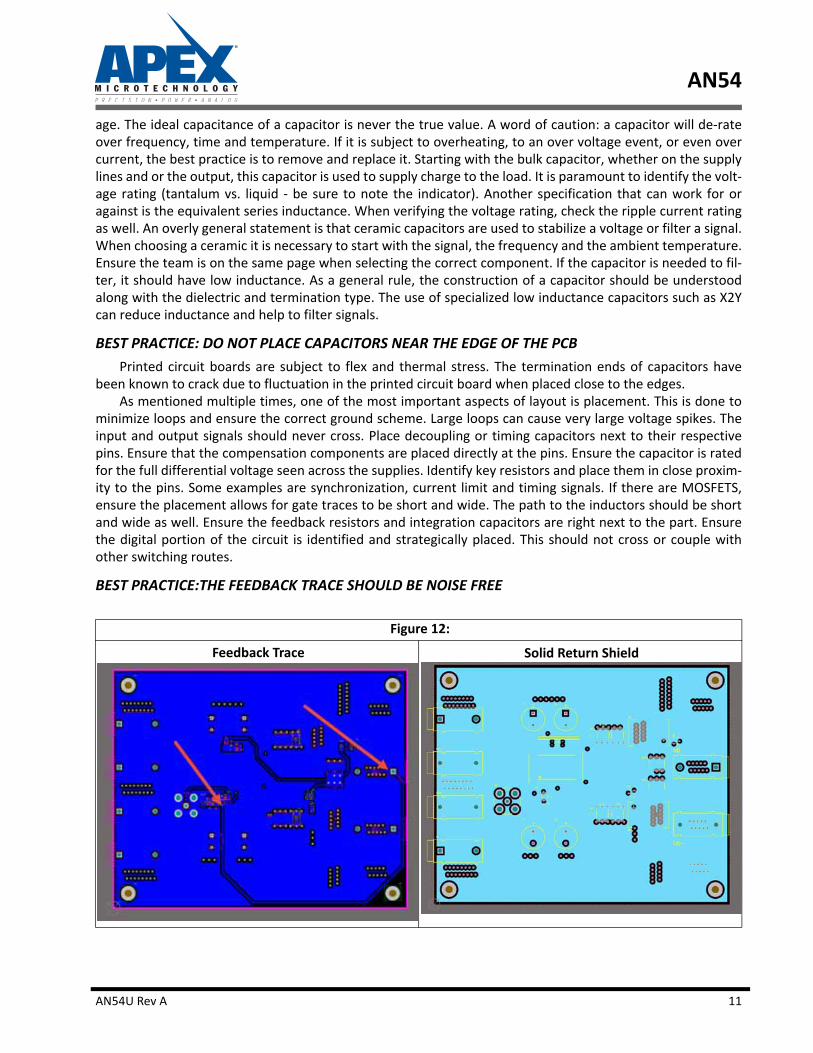
BEST PRACTICE:THE FEEDBACK TRACE SHOULD BE NOISE FREE
Figure 12:
Feedback Trace Solid Return Shield
AN54U Rev A 11

AN54
It is common practice to have the feedback trace on a small signal layer adjacent to a ground plane. Whilea via may seem to be a simple hole in a printed circuit board, their use and their structure are extremely com‐plex. The via size and annular ring should be determined by the current through the conductor. The restric‐tions of size are pre‐determined by the capability of the board house. The size and quantity should beengineered. Vias are used to move connections from one layer to another. A power via should have an adja‐cent via in order to minimize the inductance which reduces the length of the loop. For some signals it can benecessary to have two vias per pad. Vias also allow for thermal relief and the ability to more efficiently con‐duct current on multiple layers. Having too many vias defeats the purpose. An industry colloquialism refers tothis as turning a PCB into “Swiss cheese.” The PCB construction contributes to the parasitic contribution ofthe via. The inductance of the via is comprised of the height of the PCB and the diameter of the via. Thecapacitance of the via includes the hole and the anti‐pad, the height and the material (relative permittivity) ofthe PCB. It is not necessary to commit these formulas to memory; however, an understanding of how thevalue is calculated can be beneficial.
SECTION V CONCLUSION
An engineer takes a concept and creates a printed circuit board. Mathcad, spice, component tolerances,temperature variation, noise and environmental conditions are dropped into a bucket with the expectationsthat a long term solution to a complex problem will result. Some of the previously mentioned items cannotbe controlled. What can be controlled are the method and the principles of the design procedure. When thedesign team builds cohesion and synergy, the end product will always be better than if one person throws adesign at another person and expects them to finish it while the other person runs off to fight the next fire.Implementing the correct mindset for the schematic, from capture to layout, is an upfront cost that can easilypay for itself. Take the time to put in place the best case design principles and ensure that all lessons learnedare incorporated. The schematic capture paints the picture and sets the standard for the design. Take thetime to envision the printed circuit board from the inception of the schematic. Ensure the design rules andprinciples are in place. This will save the team money, time and provide increased productivity. One of thebest rewards of implementing best case design principles is that they often alleviate or even mitigate issuesthat were not conceptualizing.
Via Inductance Via Capacitance
h = Length of the viad = Diameter of the viaL= Via inductance
D2 = Diameter of clearance hole
D1 = Diameter of pad around via
T = Thickness of the PCBƐr = Relative permittivity
C = capacitance
Note: Dimension in Centimeters
Lvia 2h4hd------ 1+ln nH= Cvia
r TD1D2 D1–-------------------pF=
12 AN54U Rev A

AN54
Figure 13: PA441 with Current Buffer
Figure 14: 3D Image
5 4 3 2
-input J51
1 VRMS @ 100 kHz
V+
150V @ 5A
Power Return
-150V @ 5A
+
+ C310μF
C60.1μF
C50.1μF
C147μF
V+
RTN+
RTN-
V-
V-
+ C410μFD4
160V12
+ C210μFD3
160V12
PGND SGND
Tie Power & Signal Return on Layer 3Net Tie
RCLV-
CC2
V+CC1
VOPA
CComp
19
CC1 CC2
6.8pF
17
ILIM
ILIM15
12
21
5
7
Rbias
U1
PA441
V-
V+
Rg
1 k
Rbal
1 k
minus
plus
D5
D6
Cf
Rf
DNP
100 k
Thermal Pad
32
1 3D1
1
Rgt
0
3
1Gate t
4
RCL+
RCL+
1
2
RCL-
RCL-
13
D2 3
1
Q2
QB
QT
Vout
C722μF
C822μF
V+
C922μF
C1022μF
V-
4
-input
Rload
Vout
100Vrms @ 5A
VO
VO-
Q1
Gate b0
Rgb
FB
Place Diodes and Bypass Capacitors at the DUT Pins
AN54U Rev A 13

AN54
Figure 15: Layer 1, Power
Figure 16: Layer 2, Power
14 AN54U Rev A

AN54
Figure 17: Layer 3, Solid Return Plane
Figure 18: Layer 4, Small Signal
AN54U Rev A 15

AN54
REFERENCES:
• Chris Richardson. PCB Layout Considerations for Switchers, 2008.• Henry J. Zhang. PCB Layout Considerations for Non‐Isolated Switching Power Supplies, 2012.• TI AN‐1950. Silently Powering Low Noise Applications, 2013.• Marty Brown. Considerations in Designing the Printed Circuit Boards of Embedded Switching Supplies,
1999.• TI AN‐1149. Layout Guidelines for Switching Power Supplies, 2013.• Robert Kollman. Constructing Your Power Supply‐Layout Considerations, 2005.• TI, AN‐1229. Simple Switcher PCB Layout Guidelines, 2002.• TI, SLUA457. Single Cell Impedance Track Printed Circuit Board Layout, 2007.• Jack Ardizzoni. Fundamentals of Laying Out PC Boards, 2012.• Alterra, AN-529. Via Optimization Techniques for High-Speed Channel Designs, 2008.• Analog Devices, MT101. Decoupling Techniques, 2009.• Henry Ott. Electromagnetic Compatibility Engineering, 2009.
16 AN54U Rev A
NEED TECHNICAL HELP? CONTACT APEX SUPPORT! For all Apex Microtechnology product questions and inquiries, call toll free 800-546-2739 in North America. Forinquiries via email, please contact [email protected]. International customers can also requestsupport by contacting their local Apex Microtechnology Sales Representative. To find the one nearest to you,go to www.apexanalog.com
IMPORTANT NOTICE
Apex Microtechnology, Inc. has made every effort to insure the accuracy of the content contained in this document. However, the information is
subject to change without notice and is provided "AS IS" without warranty of any kind (expressed or implied). Apex Microtechnology reserves the right
to make changes without further notice to any specifications or products mentioned herein to improve reliability. This document is the property ofApex Microtechnology and by furnishing this information, Apex Microtechnology grants no license, expressed or implied under any patents, mask
work rights, copyrights, trademarks, trade secrets or other intellectual property rights. Apex Microtechnology owns the copyrights associated with the
information contained herein and gives consent for copies to be made of the information only for use within your organization with respect to ApexMicrotechnology integrated circuits or other products of Apex Microtechnology. This consent does not extend to other copying such as copying for
general distribution, advertising or promotional purposes, or for creating any work for resale.
APEX MICROTECHNOLOGY PRODUCTS ARE NOT DESIGNED, AUTHORIZED OR WARRANTED TO BE SUITABLE FOR USE IN PRODUCTS USED FOR LIFESUPPORT, AUTOMOTIVE SAFETY, SECURITY DEVICES, OR OTHER CRITICAL APPLICATIONS. PRODUCTS IN SUCH APPLICATIONS ARE UNDERSTOOD TO BE
FULLY AT THE CUSTOMER OR THE CUSTOMER’S RISK.
Apex Microtechnology, Apex and Apex Precision Power are trademarks of Apex Microtechnology, Inc. All other corporate names noted herein may betrademarks of their respective holders.