procedure for designing optical coatings to control · pdf fileprocedure for designing optical...
TRANSCRIPT

© 2014 Society of Vacuum Coaters 505/856-7188 157th Annual Technical Conference Proceedings, Chicago, IL May 3–8, 2014 ISSN 0737-5921
Procedure for Designing Optical Coatings to Control StressR.R. Willey, Willey Optical, Consultants, Charlevoix, MI
ABSTRACT
Residual stress in optical thin film coatings can cause adhesion failures, cracking, buckling, and bending of the substrates. The stress in the coating depends on the materials used, de-position process, and the design. The bulk properties of the coating materials and the substrate such as thermal coefficient of expansion, Young’s Modulus, Poisson’s Ratio, etc., are basic parameters to be considered. The deposition process usually yields film properties which are different from the bulk properties. These properties depend at least upon process temperature, deposition rate, and plasma assist parameters. These plasma parameters include ion species, ion voltage, and ion to atom arrival rate. The resulting film structure includes porosity, crystal form, density, non-uniformity, and possible surface and chemical interactions. The design of an optical thin film coating is mostly the refinement of the thicknesses of the layers to produce the desired reflection versus wavelength. It has been found that considerable variation in layer thicknesses can still achieve the desired spectral result. A major factor in the stress contribution of each individual layer is its thick-ness. Thin film design software can balance both the optical performance and the residual stress in the overall coating on the specific substrate with specific deposition processes, but it is first necessary to characterize the properties of the materials produced by those processes.
INTRODUCTION
The goal of this type of work is to produce a coating with a specific residual stress (usually low compressive stress) which meets certain spectral reflectance requirements. It is taken as a given that the material processes are stable, reproducible, that the stress versus thickness of the films as a function of process parameters is known, and that the coefficient of thermal expansion (CTE) of the films and the substrate are known. This paper addresses what needs to be done and the procedures needed to achieve these goals. No actual new experimental results are provided here.
Stress in optical thin films is a significant source of problems such as delamination failure of the films and distortion of the substrates on which they are coated. A principal cause of film stress is the mismatch of the CTE for the substrate and the films. Other factors affecting “intrinsic” stress in the films are thickness, deposition temperature, deposition rate, deposi-tion pressure, and ion energy and ion current when energetic processes are used. Ennos [1] provided valuable experimental information in the early days (1966) of the maturation of the technology for optical thin films.
The most recent Optical Interference Coatings conference in 2013 conducted a design problem “contest” to balance stresses and meet certain spectral performance specifications [2]. Lemarquis [3] describes his approach to the problem and the use of iso-admittance layers to solve general problems of this type. He mentions that some such problems can be solved by simply coating the second side of the substrate with a coating having the same thickness of layers with the same materials. This can be used even if all the materials are of the same stress, compressive or tensile. In order to have a stress-free coating on only one side (or controlled to be near stress-free), the included materials must be both compressive and tensile to be balanced. Recently, Oliver, et. al.. [4] reported on work to control the stresses in large optics for laser fusion experiments. It has been reported by Willey [5] that there is a great latitude available in the thickness of layers in a design which can still provide the required spectral results. This paper combines results of these works with further search of the literature to formulate a plan to acquire the necessary measurements of stress versus process variables and then design a coating to meet the optical and stress requirements.
INFORMATION FROM THE LITERATURE
Nix [6] provided an extensive review of the mechanical properties of thin films, some measurement techniques for stress, and insight into the thin film growth mechanisms from the nucleation stage through thick films. Ohring [7] shows the stress in growing films of low-mobility and high mobility materials as reproduced in Figure 1. Figure 1a shows where

2
low-mobility materials such as Cr, Fe, and Ti build tensile stress monotonically and the stress is stable in time thereafter. High-mobility materials start building tensile stress (Figure 1b) until the nucleation island growths come together (percolate) to form a continuous film and then the films become compres-sive; these mobile films then relax with time to have lower compressive or even tensile stress. The peak tensile phase for mobile materials ranges from about 100 to 600Å, depending on material. It is interesting to note in Figure 1b that aluminum, silver, and copper become almost stress-free at just about the point when they become opaque, at about 600Å.
Figures 2-4 is then multiplied by its thickness to give the stress per width for that thickness of coating as in Figure 5 (from [6]) which is what produces the final stress in the coating-substrate combination. The total stress increases more-or-less with thickness, but typically has some nonlinearities in the formative stages. This early non-linearity is ascribed to the nucleation, island forming, and then percolation of the islands into a continuous film.
Figure 1a: Film force per unit width vs film thickness (left-hand side), and time after completion of deposition (right-hand side) for low mobility growth metals: Ti, Fe, and Cr. [6]
Figure 1b: Film force per unit width vs film thickness for high-mobility growth metals: Ag, Cu, Al, and Au. [6]
Fang, et. al. [8] measured the stress progression of the in-dividual layers of HfO2 and SiO2 in a series of test coatings as shown in Figures 2 and 3. The film design for these is (1H 2L)6. They found that the first layers (darker H1 and L1) were somewhat different than later layers. Positive stress is tensile and negative stress is compressive. Ohring [7] shows a similar plot in Figure 4 for various metals, where stress is in dynes/cm2 (107 dyn/cm2 = 1 MPa). Any point on the curves of
Figure 2: HfO2 stress by layer and thickness. [8]
Figure 3: SiO2 stress by layer and thickness. [8]
The HfO2 of Figure 2 settles into a tensile stress of about 600 MPa, and the SiO2 of Figure 3 to a compressive stress of about 200 MPa. This points to a likely low stress design solution where the SiO2 layers are about three times as thick as to HfO2 layers, or a 4:1 “fencepost” design as described in Ref. 5.
Linearity could be a simplifying assumption in some cases, but the effects seen in Figures 1-4 may need to be taken into account in more refined calculations. Figure 2, in particular, settles into a fairly constant tensile stress after about 80 nm, but if we are going to adjust thicknesses in designs that have layers on the order of 80 nm or less, knowledge of the behavior

3
at thinner layers could be important. It is desirable to find as simple a model for stress versus thickness as is realistic for use in the meaningful optimization of designs with respect to stress and spectral performance.
offset (A) and a slope (B) would be needed for each process for each material to use in optimizing an optical thin film design for its spectral performance and total stress.
Force/width = Stress × Thickness = a + bt + f sin (dt) × e-ct + j sin (ht)×e-gt 1
Figure 4: Stress vs thickness for various metals [6].
Figure 5: Stress × thickness (Force/width) vs thickness for various metals [6].
Nordin [9] shows a model in Figure 6 which can be reason-ably fit to these shapes by equations of the form of an offset constant, a linear term in thickness, and two exponentially decaying sine functions as in Eqn. 1 below. Here a, b, c, d, f, g, h, and j are constants chosen to fit the measured experimental results as well as practical for use in the optimization of thick-ness for stress and spectral results. In this case e = 2.71828, and i is not used to avoid confusion. Figure 7 uses Eqn. 1 to approximately reproduce Figure 6. Also shown in Figure 7 are dotted lines for linear approximations of the curves using S × t = A + B × t, where t is the thickness and A and B are constants. These reasonably fit the more complex model from about 200Å (20 nm) to larger thickness. Therefore, only an
Figure 6: Schematic diagram of stress as a function of lamella thickness a different total pressures [9].
Figure 7: Complex and simple equation fits to Figure 6 curves.
The total stress in an optical film stack on a substrate is usually taken to be composed of the sum of the thermal stress and intrinsic (or growth) stress. The thermal stress is due to the mismatch of the coefficient of thermal expansion (CTE) of the films and the substrate. The thermal stress just depends on the CTEs of the materials involved and the temperature of the film when used versus the temperature at which the film was deposited. The intrinsic stress is a function of the deposition process and how the film grows, as illustrated in Figures 1-7.
FINDING THE STRESS VERSUS THICKNESS AND TEMPERATURE OF THE PROCESSES
Before designing to control stress, it is necessary to know the characteristics of the processes to be used for each of the materials involved. Experiments need to be performed
4
to determine these. We would then use the simplification of the linear equations for stress versus thickness illustrated in Figure 7 in the design process. The fact that these do not fit the equation well for thicknesses below 20 nm is not of concern, since one would avoid using such thin films any more than necessary due to their less dense nature before percolation occurs. This lack of full density would make films vulnerable to humidity shifts as discussed by Oliver, et. al. [4].
The goal for each of the high and low index materials will be to have as low absorption, low stress, and low a humidity shift as practical. This last goal is to avoid the complexities encountered by Oliver, et. al. [4]. High material deposition rates and hardness are desirable, but not at the expense of these top three requirements. The processes would use ion assisted deposition (IAD) with a source such as a Veeco MK-II, Kaufman & Robinson EH1000, or a DynaVac Plasma Source. The source power/current would not be a variable but would be run at maximum continuous power with 2/3 oxygen SCCM and 1/3 argon, which has been found satisfac-tory for oxide materials in past work. This maximum power allows the highest process rate. The material deposition rate would be adjusted to get the desired ion-to-atom arrival ratio (IAAR). The variables to be run using design of experiments methodology (DOE) would be drive volts (giving the eV of the ions, which are controlled by SCCM of gas flow), mate-rial deposition rates, and process temperature. The processes would be optimized for low absorption and low humidity shift. Absorption and humidity shift would be measured via spectrophotometer. The thickness would be taken from the calibrated crystal monitor readings.
Kaufman and Harper [10] point out that IAD with 1-10 eV/arriving atom is the range of ion to atom arrival ratios (IAAR) which have an effect, where the higher values are likely to give the maximum density films. With the ion/plasma source running at full power, the deposition rates would be adjusted to give the desired eV/atom or IAAR. For the DOE runs, the chosen deposition rate values would represent 1.0, 6.0, and 11 eV/atom (as close as can reasonably be estimated). The results of the DOE would show the best rate (also drive volts and temperature).
The eV of the ions might reasonably range from 80 to 180 eV with a center point of 130 eV. Willey [11] showed that this is in a practical range for all of the broad-beam sources men-tioned above. The stress in films is known to be a function of process pressure, but the eV of the IAD is determined by pressure also. Therefore, the pressure is not an independent variable in this work.
Process temperature is important for minimizing absorption and humidity shift (a function of film density), and also im-portant in controlling thermal stress. Although the process temperature range might be from near room temperature to
perhaps 300°C, it seems logical to work at lower temperatures to minimize the thermal stress. The range chosen for the DOE runs is 50, 125, and 200°C.
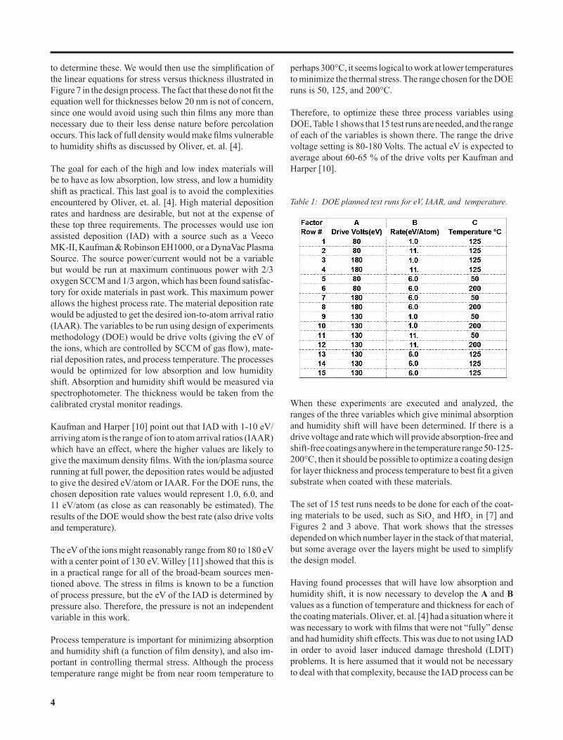
Therefore, to optimize these three process variables using DOE, Table 1 shows that 15 test runs are needed, and the range of each of the variables is shown there. The range the drive voltage setting is 80-180 Volts. The actual eV is expected to average about 60-65 % of the drive volts per Kaufman and Harper [10].
Table 1: DOE planned test runs for eV, IAAR, and temperature.
When these experiments are executed and analyzed, the ranges of the three variables which give minimal absorption and humidity shift will have been determined. If there is a drive voltage and rate which will provide absorption-free and shift-free coatings anywhere in the temperature range 50-125-200°C, then it should be possible to optimize a coating design for layer thickness and process temperature to best fit a given substrate when coated with these materials.
The set of 15 test runs needs to be done for each of the coat-ing materials to be used, such as SiO2 and HfO2 in [7] and Figures 2 and 3 above. That work shows that the stresses depended on which number layer in the stack of that material, but some average over the layers might be used to simplify the design model.
Having found processes that will have low absorption and humidity shift, it is now necessary to develop the A and B values as a function of temperature and thickness for each of the coating materials. Oliver, et. al. [4] had a situation where it was necessary to work with films that were not “fully” dense and had humidity shift effects. This was due to not using IAD in order to avoid laser induced damage threshold (LDIT) problems. It is here assumed that it would not be necessary to deal with that complexity, because the IAD process can be

5
sufficiently optimized to provide the necessary results for the coatings addressed. Table 2 shows the second DOE to develop the A and B coefficients of stress as a function of thickness, process temperature, and substrate CTE. The process used for each run would be that determined by the first DOE set for the temperature being tested. Each run would coat substrates of fused silica (FS), NBK7 glass, and some higher CTE glass such as FK51, 52, or 54. These have CTEs representing the lowest to highest expected for substrates. Equations for A and B versus thickness, temperature, and substrate CTE will be the results of this DOE data reduction. These coefficients can then be used in optical thin film design software such as FilmStar [12], with its workbook function capability, to optimize the design with respect to the optical requirements and a total film stress goal (usually low and compressive). The variables of the design optimization would include all of the layer thicknesses and the process temperature. The tem-perature would be constrained to the 50-200°C range which were characterized by the DOE and considered practical. It might also be desirable to eventually, if not at the start of the optimization, to constrain the minimum layer thickness to > 20 nm. Stresses would be measured by the Stoney [13] technique or other approaches such as the radius measuring techniques now available [6].
Table 2: DOE planned test runs for stress vs thickness and temperature.
CONCLUSIONS
Because it has been shown that individual layer thicknesses can be adjusted over a wide range and still provide a given spectral result [5], it is practical to design so as to provide a given residual stress in the total thickness of a given coating on a given substrate which also satisfies the required spectral performance. It is necessary to know the stress versus thick-ness, process temperature, and substrate CTE for each of the coating materials to be used in the optimization. It is also necessary to know the process parameters that will satisfy the other physical requirements such as low absorption and low humidity shift.
The procedures to obtain the necessary information by a series of designed experiments have been described, and simplifying assumptions and equations have been suggested.
REFERENCES
1. A. E. Ennos, “Stresses Developed in Optical Film Coat-ings,” Appl. Opt. 5, 51-62 (1966).
http://dx.doi.org/10.1364/AO.5.000051
2. K. D. Hendrix, J. D. Kruschwitz, J. Keck, “Design Prob-lem Results,” in Optical Interference Coatings (Optical Society of America, Washington, DC, 2012),TD.1.
http://dx.doi.org/10.1364/oic.2013.td.1
3. F. Lemarquis, “Athermal compensation of the stress-induced surface deflection of optical coatings usingiso-admittance layers,” Appl. Opt. 53, A229-A236 (2014).
http://dx.doi.org/10.1364/AO.53.00A229
4. J. B. Oliver, P. Kupinski, A. L. Rigatti, A. W. Schmid, J. C. Lambropoulos, S. Papernov, A. Kozlov, C. Smith, and R. D. Hand, “ Stress compensation in hafnia/silica optical coatings by inclusion of alumina layers,” Opt. Exp. 20 (15), 16597-16610 (2012).
http://dx.doi.org/10.1364/AO.53.00A229
5. R.R. Willey, “Design of Optical Thin Films Using the “Fencepost” Method,” 50th Annual Technical Conference Proceedings of the Society of Vacuum Coaters, pp. 365, 2007.
6. W. D. Nix, “Mechanical Properties of Thin Films,” Metal. Trans. A 20A, 2217-2245 (1989).
http://dx.doi.org/10.1007/BF02666659
7. M. Ohring, Material Science of Thin Films, 2nd Ed., p.745, Academic Press (2002).
Bischoff, et. al. [14] report extensive studies of HfO2 and SiO2 processes with annealing as a key element in the final adjustment of stress in application in the VUV and DUV, but which are equally applicable for our spectral regions and probable materials.

6
8. M. Fang, J-P Li, H-B He, Z. Fan, Q. Xiao, Z. Y. Li, “Evolution and Control of Optical Thin Film Stress,” Proc. of SPIE Vol. 8416 84160K-1-7 (2012).
http://dx.doi.org/10.1117/12.2009292
9. M. Nordin, M. Larsson, T. Joelsson, J. Birch, and L. Hultman, “Residual stress formation in multilayered TiN/TaN x coatings during reactive magnetron sputter deposition,” J. Vac. Sci. & Tech. A 18, 2884 (2000).
http://dx.doi.org/10.1117/12.2009292
10. H. R. Kaufman and J. M. E. Harper, “Ion doses for low-energy ion-assist applications,” J. of Vac. Sci. & Tech. A 22, 221-224 (2004).
http://dx.doi.org/10.1116/1.1633565
11. R.R. Willey, “Behavior of Three Types of Plasma Sources for Optical Coating,” 54th Annual Technical Conference Proceedings of the Society of Vacuum Coaters, pp. 323, 2011.
12. FilmStar Design from FTG Software Associates, P. O. Box 579, Princeton, New Jersey 08542.
13. G. Stoney, “The tension of metallic films deposited by electrolysis,” Proc. R. Soc. Lond. Ser. A Math. Phys. Eng. Sci. 82, 172–175 (1909).
http://dx.doi.org/10.1116/1.1633565
14. M. Bischoff, T. Nowitzki, O. Voß,1 S. Wilbrandt, and O. Stenzel,” Postdeposition treatment of IBS coatings for UV applications with optimized thin-film stress properties,” Appl. Opt. 53, A212-A220 (2014).
http://dx.doi.org/10.1364/AO.53.00A212