process development and basic studies of … · march 2001 Ł nrel/sr-520-29956 process development...
TRANSCRIPT

March 2001 NREL/SR-520-29956
V. I. Kaydanov and T. R. OhnoColorado School of MinesGolden, Colorado
Process Developmentand Basic Studies ofElectrochemically DepositedCdTe-Based Solar Cells
Annual Technical Report, Phase II16 May 199913 May 2000
National Renewable Energy Laboratory1617 Cole BoulevardGolden, Colorado 80401-3393NREL is a U.S. Department of Energy LaboratoryOperated by Midwest Research Institute •••• Battelle •••• Bechtel
Contract No. DE-AC36-99-GO10337

March 2001 NREL/SR-520-29956
Process Developmentand Basic Studies ofElectrochemically DepositedCdTe-Based Solar Cells
Annual Technical Report, Phase II16 May 199913 May 2000
V. I. Kaydanov and T. R. OhnoColorado School of MinesGolden, Colorado
NREL Technical Monitor: Bolko von RoedernPrepared under Subcontract No. XAK-8-17619-28
National Renewable Energy Laboratory1617 Cole BoulevardGolden, Colorado 80401-3393NREL is a U.S. Department of Energy LaboratoryOperated by Midwest Research Institute •••• Battelle •••• Bechtel
Contract No. DE-AC36-99-GO10337

NOTICE
This report was prepared as an account of work sponsored by an agency of the United Statesgovernment. Neither the United States government nor any agency thereof, nor any of their employees,makes any warranty, express or implied, or assumes any legal liability or responsibility for the accuracy,completeness, or usefulness of any information, apparatus, product, or process disclosed, or representsthat its use would not infringe privately owned rights. Reference herein to any specific commercialproduct, process, or service by trade name, trademark, manufacturer, or otherwise does not necessarilyconstitute or imply its endorsement, recommendation, or favoring by the United States government or anyagency thereof. The views and opinions of authors expressed herein do not necessarily state or reflectthose of the United States government or any agency thereof.
Available electronically at http://www.doe.gov/bridge
Available for a processing fee to U.S. Department of Energyand its contractors, in paper, from:
U.S. Department of EnergyOffice of Scientific and Technical InformationP.O. Box 62Oak Ridge, TN 37831-0062phone: 865.576.8401fax: 865.576.5728email: [email protected]
Available for sale to the public, in paper, from:U.S. Department of CommerceNational Technical Information Service5285 Port Royal RoadSpringfield, VA 22161phone: 800.553.6847fax: 703.605.6900email: [email protected] ordering: http://www.ntis.gov/ordering.htm
Printed on paper containing at least 50% wastepaper, including 20% postconsumer waste

i
Preface
This project, Process Development and Basic Studies of Electrochemically Deposited CdTe-BasedSolar Cells, which is performed at the Colorado School of Mines (CSM), is part of the NRELThin-Film Partnership Program. The project addresses long-term research and development issuesrelated to polycrystalline thin-film solar cells. Our general research approach is based on combiningactivities aimed at improvement of cell performance and stability with activities aimed at increasingour fundamental understanding of the properties of materials making up the cells: CdTe, CdS,multi-layer back contact, and transparent conducting oxide (TCO) front contact. We emphasize therelation between structural and electronic material properties and various processing procedures aswell as the microscopic mechanisms responsible for the cell performance and its degradation.
There is a lack of knowledge and understanding of basic issues behind the CdTe/CdS cellsperformance and stability, such as nature and electronic properties of impurities and defects thatcontrol the majority carrier concentration, mechanisms of the dopant compensation, recombinationcenters, their nature and properties, diffusion, electromigration and transformation of defects undervarious processing, stress, and operating conditions, etc. We believe that better basic understandingof the specific influence of polycrystallinity, especially for fine-grain materials like those makingup CdTe-based cells, is now one of the most important issues we must address. We need to clarifythe role of grain boundaries (GB) in forming the film electronic properties as well as those of the p-n junction. It is important to study and understand the influence of the GB boundaries on the spatialdistribution and migration of impurities and electrically active defects. To fulfill these tasks oneneeds to develop new methods and techniques (or adjust existing ones) for materialcharacterization as well as more sophisticated approaches to the data analysis and modeling. Thisreport presents studies relevant to the problems formulated above that were carried out at CSM atPhase II of the project according to the Statement of Work and Tasks of the Subcontract.
Section 1 presents studies of degradation under stressing of the cells with differently processedCdTe and different back contacts. We compared cells based on CdTe prepared by First Solar, LLC,and on CdTe electrodeposited at CSM. Back contacts were of two types: Cu/ZnTe/Au and Cu/Au.It was shown that under the same stress conditions the degradation of the cell parameters occurssignificantly different for the cells with differently prepared CdTe as well as for different backcontacts. Degradation of cells was accompanied and caused, at least partially, by significantchanges in doping profile which indicates spatial redistribution of electrically active defects andprobably non-uniform changes in compensation degree. A strong influence of bias applied duringstressing on the doping profile can be attributed to a significant contribution of electromigration tothis and perhaps to transformation of the defects in strong electric fields. The section is concludedwith an analysis of the problems to be addressed in continuing studies, including the acceptorlevels and compensating defects, deep traps, influence of grain boundaries, and deep traps. Thefollowing sections present some of our studies performed at Phase II aimed at development andchecking the validity of the approaches and methods we use for studies of basic properties of thecells and their thin film constituents.
Section 2 presents studies of deep traps in the electrodeposited CdTe cells performed incollaboration with NREL. For characterization of the cells a variety of methods were used. Alongwith routine J-V and C-V measurements, the C(V,T), C(V, f), DLTS, were also used. It was found

ii
that the C-V profile changes significantly with temperature. Two possible mechanisms behindthese changes were discussed: (a) the temperature dependence of the free hole concentration (dueto not too shallow acceptor levels and maybe to strong compensation), and (b) high concentrationof deep traps, whose contribution to the measured capacitance increases with temperature. Thesecond mechanism was verified by a strong dependence of capacitance on the testing voltagefrequency. One deep trap for electrons and four traps for holes were detected by DLTS studies.The estimated concentration of traps is comparable to the free hole concentration detected by C-Vmeasurements and depends strongly on the temperature of the Cu post-deposition annealingtemperature. The latter also influences Cu concentration detected by SIMS measurements. It wasfound that the minority-carrier lifetime reduces with increasing concentration of Cu and of thetraps located close to midgap.
Studies of spectral dependencies of photocurrent and its spatial distribution over the cross section ofthe ED CdTe cell were performed using the near field scanning optical microscopy (NSOM) (Sec.3). The instrumentation provided spatial resolution of ~1000 Å which was sufficient for revealingand mapping non-uniformities caused by the fine-granular structure of the CdTe absorber layer.Dependence of the CdTe1-xSx bandgap on S composition enabled the microscopic identification ofS-rich regions in the CdTe layer by combining NSOM with a tunable laser. S composition wasfound to be very non-uniform and greater along grain boundaries than in the grain centers,identifying grain boundaries as locations of enhanced interdiffusion. In some cross-sectionalphotocurrent images, enhancements in photocurrent were observed near grain boundaries for thephoton energies not only below but also well above the CdTe bandgap. This non-trivial effect mayprovide some guidance about the complex influence of grain boundaries on cell performance.
Impedance spectroscopy of CdTe and CdS thin films is discussed in Section 4. Measurements ofthe complex impedance in polycrystalline films are aimed at studies of electronic properties ofgrain boundaries. Based on results obtained in Phase II more complex physical and electricalmodels were developed for experimental data analysis. Some technical problems of measurementsare discussed in this section as well as their possible solutions. The results of the impedancespectroscopy studies on CdTe films with different processing stages show a dependence of the GBproperties on processing technology.
Studies of band spectrum and electron scattering in transparent conducting oxides are presented inSection 5. We discuss here details and parameters of the spectrum and scattering that relate to thefigure of merit TCOs, formulate and theoretically ground an experimental method based onsimultaneous measurements of four transport coefficients: electrical resistivity, Hall, Seebeck, andNernst-Ettingshausen coefficients. Combined with measurements of plasma and collisionfrequencies (ultra-high frequency electron transport) this method provides information on theeffective mass value, deviation from a parabolic spectrum, the shape of constant-energy surfaces,dominating scattering mechanism, and also on contribution of grain boundaries to the film sheetresistance. A brief description of principal features of the measurement equipment andexperimental procedure are presented in this section which is concluded with a review of resultsobtained so far for some TCO materials.
Appendices present data on personnel involved in the studies, laboratory improvements,and publications.
iii
Table of Contents
Preface................................................................................................................................. i
Table of Contents ................................................................................................................iiiList of Figures ..................................................................................................................... vList of Tables ....................................................................................................................... v
1. Comparison of Degradation in Vapor Transport- and Electro-DepositedCdTe Solar Cells with ZnTe:Cu/Au and Cu/Au Back Contacts
1.1 Introduction ....................................................................................................... 11.2 Experimental ..................................................................................................... 11.3 Results ............................................................................................................... 11.4 Discussion ......................................................................................................... 4
2. Deep Traps in CdTe Solar Cells2.1 Introduction ....................................................................................................... 82.2 Processing and Characteristics of the Cells Fabricated at CSM ....................... 82.3 C(V,T) and C(V, f) Dependencies ................................................................... 102.4 Deep-level Transient spectroscopy (DLTS) ..................................................... 122.5 Discussion and Conclusions ............................................................................. 15
3. Near Field Scanning Optical Microscopy (NSOM) of theCdTe/CdS Solar Cells
3.1 Introduction ....................................................................................................... 173.2 Experimental Techniques and Procedures ....................................................... 173.3 Experimental Results and Discussion .............................................................. 183.4 Conclusions ...................................................................................................... 22
4. Impedance Spectroscopy of CdTe Thin Films4.1 Introduction ...................................................................................................... 234.2 Physical and Electrical Models ........................................................................ 234.3 Experimental. Technical Problems of Measurement
4.3.1 Samples for AC characterization ........................................................... 274.3.2 Measurements in dark and light ............................................................. 28
4.4 Impedance Spectroscopy Studies of CdTe films .............................................. 29
5. Studies of Band Spectrum and Electron Scattering inTransparent Conducting Oxides
5.1 Introduction ...................................................................................................... 315.2 Electron Parameters to be Determined. Their Influence on the
TCO Figure-of-Merit5.2.1 Band model, the effective mass tensor, and density of states ................. 325.2.2 Carrier scattering, relaxation time, scattering parameter........................ 34
iv
5.2.3 Influence of non-parabolicity.................................................................. 365.3 Method of Four Coefficients
(Electron Transport in Stationary External Fields) .......................................... 375.4 Combining the Four-Coefficient Method with Optical Characterization (Ultra-High Frequency Electron Transport)
5.4.1 Basics of optical method. Conductivity effective massOptical mobility. ..................................................................................... 40
5.4.2 Evaluation of the grain boundary contributionto the film sheet resistance...................................................................... 42
5.5. Four Coefficient Measurements5.5.1 Measurement technique and experimental procedure ........................... 435.5.2 Some results and discussion .................................................................. 45
5.6. Conclusions ...................................................................................................... 45
6. References ................................................................................................. 46
7. Acknowledgements ................................................................................... 50
8. Appendices8.1 Personnel ......................................................................................................... 508.2 Laboratory Improvements ................................................................................ 518.3 Publications/Presentations* .............................................................................. 52

v
List of Figures
Figure 1.1 Changes in normalized efficiency with stress time ..................................... 2Figure 1.2 Percentage change in FF and Voc after 110 hours of stressing .................. 3Figure 1.3 Changes in doping profile for the FS-ZnTe and CSM (ED) cells
after 110 hours of stressing .......................................................................... 4Figure 2.1 The carrier concentration profile measured at room temperature
for various post-Cu annealing temperatures ................................................ 9Figure 2.2 The carrier concentration profile in the cell 150
as a function of temperature ........................................................................ 10Figure 2.3 SIMS data on the Cu concentration profile in the CdTe/CdS solar cells
with the Cu/Au back contact annealed at different temperatures:100, 150, 200, and 250oC ........................................................................... 14
Figure 3.1 Topography (a) and photocurrent (b-d) measurements takenon the cross section of a CdS/CdTe solar cell ............................................ 20
Figure 3.2 The plot showing line traces taken from single scans across the grainoutlined in Figure 3.1 ................................................................................. 21
Figure 4.1 The simplest electrical model of a polycrystalline film ............................. 23Figure 4.2 Experimental results for the resistance of a CdTe layer demonstrating
the fit to a simple one-block equivalent circuit .......................................... 25Figure 4.3 Electrical model that includes capacitance of the intragrain material ........ 26Figure 4.4 Modified electrical model for the polycrystalline film .............................. 26Figure 5.1 Comparison of two types of geometry used for the N-E measurements .... 44
List of Tables
Table 2.1 Device performance vs. Cu annealing temperature ....................................... 8Table 2.2 The trap levels and concentrations ................................................................ 13Table 2.3 Lifetime determined using TRPL in dependence
on the post-Cu annealing temperature............................................................ 15
1
1. Comparison of Degradation in Vapor Transport- and Electro- DepositedCdTe Solar Cells with ZnTe:Cu/Au and Cu/Au Back Contacts
1.1 Introduction
Almost all groups working on CdTe solar cells have used Cu-doping of CdS/CdTe solar cells viaback contact application. The positive effect of Cu mainly comes from enhancement of Voc andFF, the latter due to a significant decrease in the back contact resistance. While copper improvesthe initial performance of CdS/CdTe solar cells, it was found in many studies to deteriorate thecell stability [1, 2]. It is believed that one of the reasons is fast diffusion and electromigration ofCu in CdTe, especially along grain boundaries in polycrystalline films. That leads to expectationthat morphology of CdTe film should impact Cu migration and degradation process. Indeed,degradation rates under different stress conditions and their peculiarities reported by variousgroups are different depending on the processing techniques, type and application method of theback contact. Studies presented in this section were aimed at clarifying some of these issues.
1.2 Experimental
Two types of CdS/CdTe structures were used in this study. One was provided by First Solar,LLC, (FS). It contains about 300 nm thick CdS and wet CdCl2 treated 3.5 to 4.0 µm thick CdTeprepared with the gas transport deposition method. The other type was prepared at ColoradoSchool of Mines (CSM), containing 250 nm thick CdS (prepared with chemical bath deposition,CBD) and electrodeposited 3.3 µm thick CdTe. A wet CdCl2 treatment was given to both CdSand CdTe [3].
Two types of back contacts were applied to the FS materials: ZnTe:Cu/Au and Cu/Au. For thefirst one, thin layers of Cu (7Å) and ZnTe (500Å) were evaporated on Br2/methanol etchedCdTe, and annealed in N2 prior to evaporation of gold through mask to complete the backcontact. For the second a thin Cu layer (30Å) was evaporated on the Br2/methanol etchedsurface of CdTe and annealed in N2. The excess Cu was removed by etching in Br2/methanolsolution, and Au was evaporated to complete the back contact. Cells on the CSM material werecompleted only with the Cu/Au back contact.
All three types of cells were stressed in dark at 1000C in air under three bias conditions: opencircuit (OC), forward bias of 0.55V (FB), and reverse bias of 1.2V (RB). Cells wereperiodically taken out of the oven and cooled down to room temperature before characterizingwith I-V and C-V (at 100 kHz) techniques.
1.3 Results
Fig. 1.1 shows the efficiency degradation under FB and RB conditions for the three types ofcells: First Solar material (FS) with the first (Cu/ZnTe/Au) and the second (Cu/Au) types of backcontact, and the CSM electrodeposited (ED) CdTe with the Cu/Au back contact. Cells stressedunder FB (with any back contact) demonstrate the least degradation. FS-ZnTe cells show a

2
Fig. 1.1 Changes in normalized efficiency with stress time
decrease in efficiency by only 3% in 590 stressing hours while OC (not shown in the Figure)provided a 6% decrease for the same stressing time, and RB shows the most severe degradationof 33%. FS-Cu/Au samples show higher degree of degradation than that of the Cu/ZnTe/Ausamples and different trend in efficiency change with time. Degradation is much more severe inthe CSM (ED-Cu/Au) cells for all bias conditions, with the efficiency decreased by 80% underRB within 22 hours.
The trends in efficiency change in the initial hours of stressing are quite different for differentback contacts. FS-ZnTe cells stressed under FB first manifest a decrease in efficiency by 6%(higher than decrease in 590 hours), followed by an increase. The trend is opposite for the samesamples stressed under OC with the initial increase in efficiency followed by decrease. Cu/Auback contact on the FS material manifests different trends. FB stressed cells show an initialincrease in efficiency followed by a decrease, while OC-stressed cells show continuous decrease.Only reverse-biased cells showed almost the same trends of continuous decrease in both cases.
Pictograms in Fig.1.2 demonstrate visible differences in degradation of Voc and FF for variouscells due to different bias conditions. Differences in doping-depth profile changes after stressingcorrelate with the differences in degradation of the cell parameters. Fig.1.3 shows some data forFS-ZnTe and ED-Cu/Au samples after 110 hours stressing as compared to the initial profiles.There are two major features: (1) Doping density decreases after OC and FB stressing while it
0
0.2
0.4
0.6
0.8
1
1.2
1 10 100 1000
Stress Time (hrs)
Nor
mal
ized
Effi
cien
cy
FS-ZnTe-FB FS-ZnTe-RB FS-Cu/Au-FB
FS-Cu/Au-RB ED-Cu/Au-FB ED-Cu/Au-RB

3
Fig. 1.2. Percentage change in FF and Voc after 110 hours of stressing
-60
-50
-40
-30
-20
-10
0ZnTe-FS Cu/Au-FS Cu/Au-ED
% c
hang
e in
Voc
FBOCRB
-60
-50
-40
-30
-20
-10
0
10ZnTe-FS Cu/Au-FS Cu/Au-ED
% c
hang
e in
FF
FBOCRB

4
Fig. 1.3. Changes in doping profile for the FS-ZnTe and the CSM (ED) cells after 110hours of stressing
increases after RB stressing. This correlates with changes in the depletion width derived fromthe zero bias capacitance. (2) RB stressing causes a peak in doping profile just at the depletionlayer edge.
1.4 Discussion
We do not present in this report all the results obtained so far when studying degradation underdifferent stress conditions. It seems that the data presented above are sufficient to formulate thefollowing, rather general, conclusions:
1. The influence of the back contact type on the cell degradation and on changes in dopingprofile indicates that the Cu-related degradation process depends on the back contactstructure. It should be concluded that the role of the ZnTe interlayer is not limited toproviding low back contact resistance. Probably its presence also controls the Cu content anddistribution throughout the cell.
0.E+00
1.E+15
2.E+15
0 0.5 1 1.5 2 2.5 3Depletion width (um)
Dop
ing
den.
(cm
^-3)
0 hr-FS OC-FS FB-FS
RB-FS 0 hr-ED RB-ED
5
2. For the same back contact, degradation varies with the CdTe processing. Presumably itoccurs due to differences in the film morphology and the grain boundary properties as well asin imperfection of the intra-grain material.
3. Degradation of cells is accompanied and caused, at least partially, by significant changes indoping profile, which indicates spatial redistribution of electrically active defects. A stronginfluence of the applied bias during stressing should be attributed to a significant contributionof electromigration to this redistribution and maybe also to transformation of the defects instrong electric fields.
We are continuing stress experiments by broadening the variety of stress conditions and theircombinations (light, dark, temperature, bias applied). In phase III we plan to study degradation inthe cells fabricated with other processing techniques, such as CSS CdTe, APCVD CdTe, andsputtered CdS. These studies will provide richer and more detailed information for discussion ofpossible mechanisms of degradation.
However, we believe that it is even more important to study in more detail structural andelectronic properties of the cells and their changes with varying processing procedures and due tostress testing. Only in this way we will be able to provide a solid scientific basis for clarifyingthe degradation mechanisms. Below we present some problems we are focussed on.
1. One of the high priority issues is the problem of the electrically active centers that determinethe majority carrier concentration. Doping with Cu is commonly used to control the holeconcentration in CdTe, but its concentration in CdTe detected by SIMS [4, 5] is orders ofmagnitude higher than the hole concentration provided by C-V profiling. This discrepancy isnot specific for some processing method but is common for all. The major questions to beaddressed are:
(a) What Cu-related defects dominate creation of free holes in CdTe: CuCd, Cu-containedcomplexes, or acceptor-type native defects whose concentration depends on presence andconcentration of Cu?
(b) What are the energy levels provided by the dominating acceptor centers: are those levelsshallow or not, in other words, are they completely thermally ionized at roomtemperature or not? Most reports attribute the acceptor level of EA-EV ~ 0.3-0.35 eVfound in CdTe:Cu to CuCd. This level is deep enough to be much less than half thermallyionized at T=300 K, if the concentration of the centers exceeds 1014cm-3. For example, ifEA-EV=0.35 eV and NCuCd ≈1016 cm-3, the estimated free hole concentration at T=300Kshould be of nh ≈ 5×1014 cm-3.
(c) Does a huge difference between NCu and nh comes from involvement of the majority ofCu atoms in some neutral precipitates or neutral complexes? Or is there a high degreecompensation of the acceptor centers by donor centers provided by Cui, or native defectsor some complexes? For the shallow acceptors nh= NA-ND, hence if nh<<NA, thecompensation degree is close to unity ( 1/ ≈AD NN ). Even a small change in the ratio

6
ND /NA can lead to a significant, by orders, change in the free hole concentration. Itshould be mentioned that in the case of deep dominating acceptors, the influence ofcompensation on the hole concentration could be even stronger than for shallowacceptors. For the deep acceptor like that in the example above (EA-EV=0.35 eV),nh ≈2×1013cm-3, if NA τ 1015cm-3 and ND /NA ≈ 0.5, no matter what is the real NA value.Variation of the ND /NA value impacts the hole concentration much weaker than in theprevious case, unless this ratio comes close to either 0 or 1.
(d) What is the influence of the deep electronic states associated with grain boundaries (GB)on the hole concentration in CdTe? Previous studies of the CdTe bicrystals [6] andpolycrystalline thin films [7, 8] showed that in the latter with a grain size of ~ 1 µ, thenumber of the GB states per unit volume can be as high as 1016 to 1017cm-3. That meansthat the GB states can effectively compensate acceptors in the grain volume (deplete thegrain bulk). The difference between this compensation mechanism and that consideredabove is that in the previous case the film is overall as well as locally neutral, while in thelatter case grain boundaries are charged positively and the grain bulk is chargednegatively, so that film is neutral as a whole but not locally. It should be mentioned thatin the case of dominating compensation by the GB states, the negative space chargedensity in the GB proximity, should be close to NA and can be much higher than the freehole concentration derived from the C-V profile. Thus the enhanced space charge density(10×1017cm-3) in the GB region observed in [7, 8] may be explained in particular by theGB compensation mechanism, although accumulation of the acceptor-type defects in theGB region also cannot be excluded.
(e) Another important issue to be addressed is the presence of deep traps and their influenceon recombination processes. Although a few publications are devoted to detection andstudies of deep traps in CdTe, e.g., [9-12], the problem is far from clear. Numerous deeptrap levels were reported so far, but the centers responsible for them have not beenidentified unambiguously. The sets of the deep levels reported in different publicationsare not the same and depend on the processing technology, postdeposition treatment, andmorphology of polycrystalline films. That leads to an additional uncertainty inidentification of the centers. One may expect that some of deep levels detected in the thinfilm CdTe-based solar cells originate from the CdTe/CdS interface and from the GB’sinside the CdTe layer.
2. If one believes that a high compensation degree takes place in CdTe, it is reasonable toexpect deep traps of high concentration, higher than the free hole concentration. These trapscan influence the magnitude and spatial distribution of the space charge, hence the “dopinglevel”- depth profile obtained with the standard analysis of C-V measurements. It is believedthat GB affect strongly the cell performance. The role and mechanisms of their influence onthe electronic properties of thin film CdTe solar cells are not understood properly. Here wewill discuss some of them:
(a) Presence of potential barriers for the majority carriers at the GB was demonstrated bothfor the CdTe bicrystals and polycrystalline films, see e.g., [6-8]. That means two- orthree-dimensional non-uniformity in the electrostatic potential distribution, hence rather

7
non-uniform electron transport in thin-film CdTe cells. Potential relief separates spatiallyelectrons and holes reducing the recombination rate. On the other hand, deep GB statesthat are responsible for the potential barriers can act themselves as the recombinationcenters.
(b) Diffusion of impurities and defects may be expected to be faster along the grainboundaries. This expectation was verified for interdiffusion at the CdTe/CdS interface[13, 14]. It was shown, although indirectly, that concentration of the ternary phase andthe S content is higher in the GB regions. The evidence of rapid diffusion of Cu inpolycrystalline CdTe due to GB was clearly demonstrated in [15]. Probably the rates ofelectromigration, which is well manifested for Cu in CdTe are also different for the bulkmaterial and the GB regions. GB are prone to attract and accumulate structural defectsand impurities as well as to serve as nuclei for precipitates. It should be mentioned thatusually we are not well aware whether these effects are beneficial (e.g. passivation ofgrain boundaries, whatever it means) or detrimental for the cell performance. Anyway,grain boundaries can strongly affect the spatial distribution of the species vital for the cellperformance, especially in the fine grain structures like CdTe and CdS thin films.Migration along the GB, especially for fast diffusing species such as Cu, should also leadto their significant redistribution under varying stress conditions and hence may be animportant factor in the degradation processes.
The following sections present some of our studies performed at Phase II and aimed atdevelopment and checking validity of some approaches we use for studies of basic properties ofthe cells and their thin film constituents.
8
2. Deep Traps in CdTe Solar Cells
2.1 Introduction
As mentioned in Sec. 1.4, the problem of detection, identification and studying the properties ofdeep traps in the cell is an important issue relevant both to the cell performance and to itsdegradation. Recently we started these studies in collaboration with Dr. R. Ahrenkiel, and Dr. D.Levi (NREL). As in studies presented in the previous section we were interested in comparisonof properties of differently processed CdTe/CdS cells. Ahmet Balcioglu (the CSM Ph.D. studentadvised by Dr. Ahrienkel) was studying the Cu-related deep traps in the CdTe/CdS solar cellsfabricated at NREL (CBD CdS, CSS CdTe, and Hg:Cu/graphite back contact) using C-V, C-T,DLTS and ODLTS techniques. Balcioglus Ph. D. research included similar studies of our cells(CBD CdS, electrodeposited CdTe, and Cu/Au back contact). To date we can compare the resultsfor only the as-prepared cells. Studies of changes caused by stress testing in the CSM cells areintended for Phase III, so that in our Final Report to NREL we will be able to present andanalyze differences between the NREL and CSM degraded cells.
2.2 Processing and Characteristics of the Cells Fabricated at CSM
The cells were processed with only small deviations from our standard procedure. The 250 nmthick CdS layer was deposited on commercial tin oxide/glass substrate and annealed with CdCl2in N2 for 50 min at 450oC. After electrodepositing ~3 µm thick CdTe, the obtained structure wassubjected to CdCl2 treatment in air for 45 min at 410oC. After etching with 0.1% Br2/methanol,the Cu layers of 30 or 100 Å thickness were thermally evaporated on the CdTe surface followedby annealing at temperatures ranging from 100o to 250o C for 15 min in vacuum. Afterwards, aBr2/methanol etch was applied to remove the remaining Cu from the CdTe surface. Metallizationof the back contact was provided by thermal evaporation of gold.
The J-V characteristics of completed cells were measured using an ELH-type tungsten-halogenlamp calibrated with a GaAs standard cell and providing the 1 Sun intensity of light. The resultsof J-V characterization for the cells prepared with different temperature of the post-Cu annealingare presented in Table 2.1.
Table 2.1 Device performance vs. Cu annealing temperature
TemperatureoC
Efficiency%
JscmA/cm2
VocmV
RsΩ-cm2
RshΩ-cm2
FF%
100 7.00 21.5 670 40.0 230 49140* 9.00 20.9 732 2.60 475 59150 10.6 22.8 725 7.00 560 64170* 8.10 20.4 728 7.70 409 54200 8.50 22.1 658 9.10 316 59250 5.30 19.3 564 12.8 190 48
9
The highest efficiency was demonstrated by the cell with 150oC post-Cu annealing temperature.Efficiency decreases as the annealing temperature goes up or down from 150oC. As to theparticular cell parameters (Voc, Jsc, etc.), the 150 cell has the highest Jsc, Rsh and FF values. Vocis only a little lower than that for the neighboring cells, 140* and 170* that were processedwith 100 Å thick Cu films. These two cells demonstrate considerably lower Jsc.
Standard C-V measurements to determine the apparent doping profile were performed at afrequency f=100 kHz using the standard treatment of the data based on the equation [16]:
( ) 120
2 /12
−
=
dVCdqAN εε
(2.1)
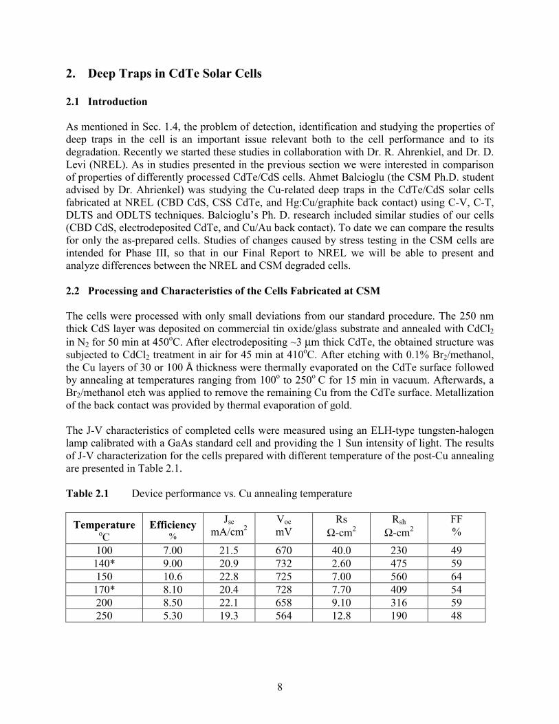
where C is the measured capacitance, V is the applied bias voltage, A is the area of a cell. Thecarrier concentration profiles determined for the cells listed in Table 2.1 are shown at Fig. 2.1.
It is to be noted that the doping level increases with the annealing temperature and that thislevel rises at smaller depths, that is closer to the CdS/CdTe interface. For the 150 cell thedoping density at zero and reverse biases is close to that for the NREL CSS cells, but at theforward biases exceeds those by more than an order of magnitude. The discrepancy for the 200and 250 cells is remarkably higher.
Fig. 2.1 The carrier concentration profile measured at room temperature for variouspost-Cu annealing temperatures
3.02.52.01.51.00.50.010 13
10 14
10 15
10 16
10 17
ED100
ED150
ED200
ED250
ED140*
ED170*
Depth (µm)
Car
rier C
once
ntra
tion
(cm
)-3
10
2.3 C(V, T) and C(V, f) Dependencies
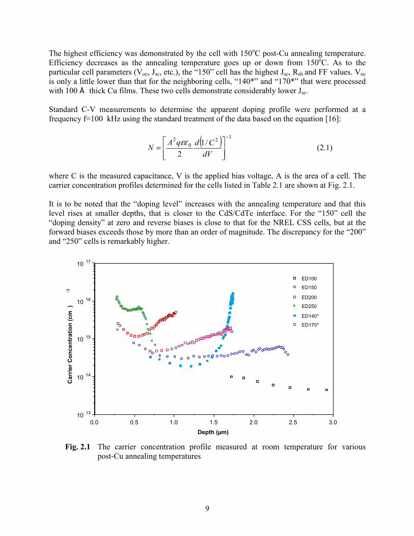
Fig. 2.2 shows the temperature dependence of carrier concentration derived from the C-Vmeasurements for the cell 150. A remarkable decrease is seen as temperature changes from400 K to 150 K. It should be also mentioned that the capacitance dependence on bias weakenswith decreasing temperature. For measurements at 150 K the C value changes by about 5% in thebias range from 1.8V to +0.2V. At T=100 K no change in capacitance could be seen in the samebias range and the depletion width estimated from the capacitance is very close to the CdTe layerthickness. One of probable explanations for this C(T) behavior is carrier freeze-out. If so, onecan suppose that the impurity level that provides the dominating contribution to the holeconcentration is not shallow, or that it is strongly compensated.
Fig. 2.2 The carrier concentration-depth profile in the cell 150 as a function of temperature
Another possible mechanism of the temperature-dependent capacitance is the influence of deeptraps. It is known that in the presence of deep traps two distinct components of the measuredcapacitance should be considered [16]. The first one is described as the geometry or depletioncapacitance, Cd, which is determined by the depletion width and does not depend on the testingvoltage frequency, ω (the angular frequency ω [rad/s]=2πf [Hz]). The second component is dueto oscillations of the electrical charge trapped by deep levels, named the oscillation capacitance,CT. The amplitude of these oscillations and hence the magnitude of CT depends strongly on therelationship between ω and the characteristic frequency of traps, ωo, which is reciprocal of thecharacteristic time, τ. For high testing frequencies, ω>>ωo, the trapped charge cannot follow
321010 14
10 15
10 16
400 K350 K294 K250 K200 K150 K
Depth (µm)
Car
rier C
once
ntra
tion
(cm
)-3

11
changes of the testing voltage and the CT value tends to zero. As frequency ω decreases,becoming of the order of ωo or lower, the CT value increases and tends to saturation at the levelthat depends on the trap concentration. Thus the reduction of the measured capacitance with thetesting frequency could be considered as an indication of the deep traps presence.
C-V measurements were performed on the cell 150 at room temperature at testing frequenciesof 0.1, 1, 10, and 100 kHz. The frequency-dependent capacitance was observed over all the biasrange from 2 V to +0.5 V. Reduction of capacitance with frequency was much morepronounced at zero and forward biases than at the reverse bias. Indeed, for V=0 and V=+0.5 vthe measured capacitance decreases 2.5 times as frequency rises from 0.1 kHz to 100 kHz, whileat V= -2 V the decrease is only of about 25 %. These data show that there exist deep traps inamount comparable to the carrier concentration or even higher, and that the traps are probablydistributed non-uniformly over the CdTe thickness.
One more conclusion can be made from these measurements, namely from a rather smooth C(f)dependence. Indeed, the C(f)/C(0.1 kHz) ratio measured at V=0, is equal to 0.7, 0.5 and 0.4 forf=1 kHz, 10 kHz and 100 kHz, respectively. For a single trap level with a certain characteristicfrequency ωo, the CT(ω) dependence is described by the equation:
( )( )2/1
1)0(o
TT CCωω
ω+
= (2.2)
A significant change in CT with ω takes place close to ωo. In the range of ω=(1/5-5)ωo, CT(ω)changes from 0.96CT(0) to 0.04CT(0). At lower and higher frequencies the measured capacitanceapproaches rapidly the saturation levels, C0=CT(0)+Cd and C∞=Cd, respectively. In ourmeasurements C value changed gradually as the testing frequency ω increased by three orders ofmagnitude. That means that there are several trap levels, possibly spread over some range ofenergies within the bandgap.
Based on the deep trap concept, we can discuss an alternative explanation for the temperaturedependence of capacitance. The characteristic time/frequency of a trap depends on emission rateand varies exponentially with temperature: ωo∝ exp(-∆E/kBT), where ∆E is the distance betweenthe trap level ET and the edge of the corresponding band, that is ∆E=ET-EV if we consider trapsfor holes. Thus the traps that are too slow at room temperature to follow the oscillatingvoltage, become players when their ωo approaches ω due to enhanced temperature. It is seenfrom Eq. 2.2 that contribution of traps to the capacitance measured at some frequency ω, CT(ω),increases with rising ωo, approaching the limiting value CT(0). The CT(0) value is determined bythe trap concentration, its distribution over the diode thickness, and band bending [16].
While the second mechanism (deep trap contribution) is supported by the data presented above,the first one (increase in carrier concentration with temperature) is also rather probable. It is to benoted that the data presented at Fig. 2.2 were obtained at high frequency of 1 MHz, hence thecontribution of deep traps to the total measured capacitance, that is the ratio CT/(CT+Cd), wasminimized as much as possible. To clarify the role and estimate the individual contributions ofthese two mechanisms we need to perform more thorough experimental studies and modeling.
12
We are planning more detailed studies of C(V, f, T) dependencies on the cells with varying Cucontent and processing procedures. These measurements will be made in dark and light andhopefully will enable detecting deep traps and studying their characteristics, such asconcentration, spatial distribution, energy levels or density of states function, etc. We currentlyhave two LCR meters that cover together the frequency range from 20 Hz to 30 MHz. We arefinishing building a chamber for measurements at temperatures above as well as below roomtemperature. We believe that it would be worthwhile to supplement the C(V, f, T) studies withmeasurements of the Hall effect (as well as photo-Hall) at different temperatures on the dopedand undoped CdTe thin films. The Bio-Rad Hall system we possess provides measurements inthe temperature range from about 100 K to 450 K. Recently we have supplied this system with alight source based on the array of the light emitting diodes. Currently we are designing thesystem that will illuminate the sample with white light using fiber optics.
We have started modeling C-V profiles in the cells with deep traps. The first step was modelingCd-V profile (high frequency capacitance) for the cells with uniformly distributed acceptors(uniform doping level). It was shown that in the trap presence the apparent doping profile,obtained with a common method based on Eq. 2.1, can be rather non-uniform. In particular, itcan manifest a sharp increase at high reverse bias voltages. This feature is commonly observed inthe cells doped with Cu via the back contact application. Usually it is attributed to the enhanceddopant concentration near the back contact. The non-uniformly distributed traps can also imitatesome peaks in the apparent doping profile similar to those observed in the cells stressed at thereverse bias, see Fig. 1.3.
2.4 DeepLevel Transient Spectroscopy (DLTS).
All the DLTS studies were performed at NREL as well as the minority-carrier lifetime and SIMSmeasurements. The DLTS measurements were used to determine the energy of deep levels in thebandgap and estimate the trap concentration. These measurements were done at a reverse bias of1.0 V with pulse amplitude of 1V and pulse width of 1.0 ms. The concentration of trap levelswas estimated using equation 2.3 [from Ref. 16]:
−−−∆= 22
2
)()(2
λλ oT ww
wNCCN (2.3)
where ∆C, C, N=(NA-ND), w, wo and λ are the DLTS peak maximum, steady state capacitance ofa peak maximum, the carrier concentration, the depletion width at reverse bias, depletion widthat forward bias, and the edge region. The latter is defined as a distance from the depletion regionedge and to the plane where the trap level crosses the Fermi level (crossing point).
Five deep levels were observed in devices studied in the temperature range of 80 to 450 K. Theywere designated as E1 (the electron trap), H1, H2, H3, and H4 (all four are the hole traps). Theirenergies are presented in Table 2.2. It was found that the deep levels were partially annealed as aresult of the DLTS scan from 80 to 450 K. The repeated scan revealed reduction of the trapconcentration and a significant change in the peak shape. The trap concentrations calculatedusing the initial DLTS spectra (the first scan 80-450K) are also shown in Table 2.2. The trap

13
levels H1, H2, and H3 were derived from the DLTS spectra obtained on the partially annealedsamples because at the initial scan the DLTS peaks did not shift with the emission rate window.It might be due to the presence of the interfacial layers, non-exponential transients, and largeseries resistance of a cell.
Table 2.2. The trap levels and concentrations
Trap level energy
E1
Ec-0.37 eV
H1
Ev+0.34 eV
H2
Ev+0.70 eV
H3
Ev+0.70 eV
H4
Ev+0.97 eV
Sample ID
(Cu anneal
Temperature)
Trap concentration
(cm-3)
100 9.7x10¹¹ - 5.6x10¹³ 7.7x10¹³ -
150 3.2x10¹³ - 1.5x10¹⁴ 1.8x10¹⁴ -
200 - 3.5x10¹² 3.0x10¹⁴ 3.9x10¹⁴ 6.5x10¹⁴
250 - 2.5x10¹³ - 5.2x10¹⁴ 1.2x10¹⁵
The estimated concentration of traps is pretty high being comparable to the doping levelderived from C-V measurements (the free carrier concentration), especially for the deepestH2, H3, and H4 levels. The observed increase in the trap concentration with increasing post-Cuannealing temperature correlates with the increase of Cu concentration in the CdTe indicated bySIMS measurements performed at NREL by Drs. S. Asher and R. Reedy, see Fig. 2.3.
Five deep levels were also revealed in the NREL CSS devices [17, 18] of the level energy :E1*=Ec-0.28eV, H1*=EV+0.35eV, H2*=EV+0.45eV, H3*=EV+0.79eV, and H4*=EV+0.93eV.These energies are close to those found in the CSM cells except the H2* and H2 levels. Probablythe other four levels are associated with the same types of defects in both materials. Smalldifference in energy for similar states observed in the two materials should not be considered asevidence of a different nature of the defects. Indeed, it could be seen from literature that theestimates in various reports of the levels attributed to the same centers vary depending on themethod of the CdTe cell preparation and the CdTe postdeposition treatment. Abou-Elfotouh et.al. [11] observed in the ED-grown CdTe devices a minority carrier trap level with an activationenergy of Ec-0.35eV. In as-grown CSS CdTe/CdS cells the E1 level has an activation energy ofEc-0.28 eV [17,18]. After stressing of a cell this level shifts into the band gap by 0.22eV [17].The H1 level of energy about Ev+0.35 eV was previously reported for the ED-grown,

14
Fig. 2.3 SIMS data on the Cu concentration profile in the CdTe/CdS solar cells withthe Cu/Au back contact annealed at different temperatures: 100, 150, 200 and250o C.
CSS-grown CdTe devices [11, 12, 18, 20, 21] and p-CdTe single crystals [10, 12, 22]. Usually itis attributed to CuCd substitution defects. The H3 level with the energy around Ev+0.8eV wasreported in numerous publications and is believed to be associated with an acceptor complexinvolving the native VCd defect and impurity.
The concentration of levels E1 and H1 are comparable for both the NREL and CSM devices. Theconcentration of H2 traps was two orders of magnitude higher in the CSM devices.Concentrations of H3 and H4 traps were also significantly higher for the CSM cells.
It is to be noted that for the trap H3 with an activation energy close to the CdTe midgap, thethermal emission rates were found comparable for electrons and holes [23]. This indicates thatthese traps can act as effective recombination centers. To confirm this, the minority-carrierlifetime was measured in the CSM cells using time-resolved photoluminescence (TRPL). Thelifetime was found to depend on the post-Cu annealing temperature and hence the trapconcentration. The data presented in Table 2.3 show the tendency of the lifetime to reduce withincreasing trap density. The latter increases with the annealing temperature and, as seen fromFig. 2.3, with the Cu content in CdTe.
321010 17
10 18
10 19
10 20
100150200250
Depth (µm)
Cu
Con
cent
ratio
n (c
m-3
)
Back Contact CdTe layer Interface
Au contact
15
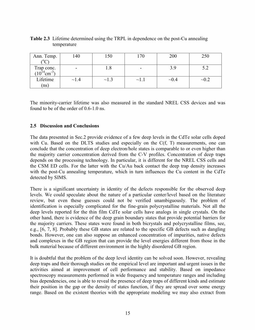
Table 2.3 Lifetime determined using the TRPL in dependence on the post-Cu annealing temperature
Ann. Temp.(oC)
140 150 170 200 250
Trap conc.(1014cm-3)
- 1.8 - 3.9 5.2
Lifetime(ns)
~1.4 ~1.3 ~1.1 ~0.4 ~0.2
The minority-carrier lifetime was also measured in the standard NREL CSS devices and wasfound to be of the order of 0.6-1.0 ns.
2.5 Discussion and Conclusions
The data presented in Sec.2 provide evidence of a few deep levels in the CdTe solar cells dopedwith Cu. Based on the DLTS studies and especially on the C(f, T) measurements, one canconclude that the concentration of deep electron/hole states is comparable to or even higher thanthe majority carrier concentration derived from the C-V profiles. Concentration of deep trapsdepends on the processing technology. In particular, it is different for the NREL CSS cells andthe CSM ED cells. For the latter with the Cu/Au back contact the deep trap density increaseswith the post-Cu annealing temperature, which in turn influences the Cu content in the CdTedetected by SIMS.
There is a significant uncertainty in identity of the defects responsible for the observed deeplevels. We could speculate about the nature of a particular center/level based on the literaturereview, but even these guesses could not be verified unambiguously. The problem ofidentification is especially complicated for the fine-grain polycrystalline materials. Not all thedeep levels reported for the thin film CdTe solar cells have analogs in single crystals. On theother hand, there is evidence of the deep grain boundary states that provide potential barriers forthe majority carriers. These states were found in both bicrystals and polycrystalline films, see,e.g., [6, 7, 8]. Probably these GB states are related to the specific GB defects such as danglingbonds. However, one can also suppose an enhanced concentration of impurities, native defectsand complexes in the GB region that can provide the level energies different from those in thebulk material because of different environment in the highly disordered GB region.
It is doubtful that the problem of the deep level identity can be solved soon. However, revealingdeep traps and their thorough studies on the empirical level are important and urgent issues in theactivities aimed at improvement of cell performance and stability. Based on impedancespectroscopy measurements performed in wide frequency and temperature ranges and includingbias dependencies, one is able to reveal the presence of deep traps of different kinds and estimatetheir position in the gap or the density of states function, if they are spread over some energyrange. Based on the existent theories with the appropriate modeling we may also extract from

16
these measurements the emission rate, capture cross-section, concentration and spatialdistribution. DLTS, ODLTS, and measurements of lifetime by means of TRPL provide valuableinformation.
Simultaneously we must establish and explain (using modeling) correlations between thedetermined trap characteristics, on one hand, and the cell photo-electrical parameters, such asVoc, Jsc, Rse etc., on the other. We need also to analyze the deep trap influence on the C-V profileand correct the doping level profile derived. Finally, the trap characteristics and the cellperformance should be related to the cell processing techniques and regimes to provide the basisfor optimizing the latter.

17
3. Near Field Scanning Optical Microscopy (NSOM)of the CdTe/CdS Solar Cells.
3.1 Introduction
To clarify the role of polycrystallinity in forming opto-electronic properties of thin filmCdTe/CdS solar cells, it is important to use characterization techniques with a high spatialresolution. Morphological studies (SEM, AFM) of the CdTe absorber layer show that the grainsize is usually in a range of one to several microns. Hence we need the tools that provide testingof composition, optical and electronic properties of a material with a spatial resolution on theorder of 0.1µm or lower. Along with the scanning tunneling microscopy and spectroscopy, theNSOM is one of the most promising techniques. In our facilities this method and instrumentationwere developed by Professor R.T. Collins and Graduate Research Assistant M.K. Herndon. Inthis section we present some results that demonstrate effectiveness of NSOM for studies andtwo-dimension mapping of current collection over the cell cross section. One of the major goalsof the experiments was to study the interdiffusion of S into CdTe by using the compositionaldependence of the ternary CdTe1-xSx phase band gap and NSOM.
Post growth annealing of the CdTe/CdS films has been shown to enhance the performance ofsolar cells. Substantial evidence exists that interdiffusion between CdTe and CdS layers occursduring growth and post growth annealing processes [13]. In particular, S diffusion into the CdTelayer leads to the formation of a ternary CdTe1-xSx phase within the CdTe layer. For Sconcentrations less than ~25% , bowing in the bandgap of the ternary as a function of x reducesthe band gap as S content increases. This leads to a decrease in the low energy cutoff of thedevice relative to pure CdTe [24]. Various models for the mechanism of S diffusion have beendeveloped, and it is generally believed that grain boundaries must play a role in the diffusionprocess. This has been difficult, however, to verify experimentally. This study provides evidencethat S diffuses preferentially along the grain boundaries in CdTe.
3.2 Experimental Techniques and Procedures
The samples used in these measurements were grown on soda-lime glass coated with a tin oxideTCO. Chemical bath deposition was used to grow a ~200nm thick CdS layer on the SnO2. CdTewas electrochemically deposited on the CdS layer to a thickness of 3-4 µm. The sample wastreated with CdCl2 and annealed at 365oC. Previous work has shown interdiffusion can beobserved after the 365°C anneal, and increases significantly with temperature. By 450°C, anearly uniform S concentration is observed throughout the film [14]. Gold was evaporatedthrough a shadow mask to form a back contact and define individual devices. Capacitance-voltage measurements gave a zero bias depletion width of ~1.5 µm for the diodes and dopinglevel of ~5 x10¹⁴/cm3 in the CdTe.

18
The glass side of the sample was scribed in the region under a device and broken to expose across section of the device. It was mounted so that spatially resolved photocurrent andtopographic images of the cross section could be measured with the NSOM. The NSOM is ahome built instrument that operates in air. The experiments were done at room temperature. TheNSOM probe was made from a single mode optical fiber which was tapered using a micropipettepuller and metal-coated, leaving a ~100nm diameter aperture at the tip [25]. The probe was rasterscanned across the sample cross section using optically detected shear force feedback to maintaina constant separation of approximately 10nm between the probe tip and sample [26]. Monitoringthe feedback signal while raster scanning the sample allowed the topography of the cleavedsurface to be measured.
A tunable Ti:Sapphire laser and a 632.8nm HeNe laser were simultaneously coupled into thefiber probe allowing it to be used as an excitation source. Each laser was chopped at a differentfrequency before being coupled into the fiber. The photocurrent generated in the CdS/CdTediode was detected for each wavelength using two lock-in amplifiers. The outputs of the lock-inamplifiers were recorded at each point as the sample was scanned. This allowed two spatially-resolved measurements of the generated photocurrent, one for each wavelength of light, to berecorded simultaneously with the surface topography.
Scans of the cell cross section began on the glass side of the junction, and progressed toward theback of the CdTe layer. The same area was scanned several times, each with a differentwavelength from the Ti:Sapphire laser, in order to see variations in collection as a function ofexcitation energy. The HeNe images, taken simultaneously with each Ti:Sapphire measurement,were compared from scan to scan. This reference enabled us to ensure that variations in theTi:Sapphire measurements were due to changes in excitation wavelength and not due to changesin the probe or scanning conditions.
The band gap of the CdTe1-xSx ternary phase decreases as a function of x (for x ≤ 0.25) from~1.51eV at x=0 to 1.41eV at x=0.25 [27-29]. This dependence of band gap on x allows changesin excitation energy during NSOM measurements to be used to observe spatial variations in the Scomposition of the CdTe1-xSx ternary across the heterojunction, and therefore to identify regionsof high S content. In the discussion below we have used the bandgap dependence of Ref. 28 toassociate optical excitation energies with specific S concentrations. In general, however, theband edge of polycrystalline films shows inhomogeneous broadening due to effects such asstrain, defects, and alloying, which can lead to an apparent bandgap which is lower than that forcrystalline material. Because of this broadening and the uncertainties in the reported compositiondependence of the CdTe1-xSx band gap, relative changes and spatial variations in S compositionfound from optical measurements are likely to be much more reliable than the numerical Scompositions inferred from the measurements. The later should probably be viewed as correct towithin a few percent.
3.3 Experimental Results and Discussion
Figure 3.1 shows a topographic image and three photocurrent images, each produced using adifferent excitation energy. The images are 4.8 x 4.8 µm. The topography measurements showed

19
an average grain size of 1-2 µm. A small amount of drift occurred between scans. Comparison ofthe locations of individual grains seen in the topographic images allows us to track this drift. Thelayers present in the film have been identified adjacent to Figs. 3.1a and 3.1b. The interfacebetween the glass and film is evident as the horizontal feature across the bottom of thetopography image. One obvious grain, which will be discussed in more detail below, has beenoutlined on the topography plot (Fig. 3.1(a)). The topography measurements obtained in registrywith each photocurrent measurement were used to locate this feature in subsequent scans,allowing this region to be identified in the photocurrent images in Figs. 3.1(b)-3.1(d).
For 1.615 eV excitation (Fig.3.1(b)), which is a little more than 100 meV above the CdTebandgap, we see the photocurrent is strongly peaked near the junction, and decreases toward theback of the device. This is typical of measurements at energies above bandgap. In general, thephotocurrent becomes even more strongly peaked near the CdTe/CdS junction as energyincreases. As energy decreases below the CdTe bandgap to 1.463eV (Fig. 3.1(c)), correspondingto a S composition of 6%, the collection efficiency at the back of the device improves relative tothat at the interface. We have observed this effect (a widening of the collection region at longerwavelength) in most edge cleaved semiconductor diodes we have studied. We attribute it to acompetition between surface recombination and collection by the junction. At longerwavelengths, the light is absorbed further from the surface, allowing more of the carriers to becollected by the junction before recombining at the surface. Similar observations and conclusionswere presented in Ref. 30. We note that the carrier collection region at this energy extends fromthe junction to the back of the device and that the average collection efficiency at the junctionand near the back are roughly the same. Simplistically, the width of the collection region isdetermined by the depletion width and the minority carrier diffusion length. Since our depletionwidth is ~1.5µm, this indicates a minority carrier diffusion length of more than 2µm.
At 1.422eV (Fig.3.1(d)), the excitation energy is 80meV below the CdTe band gap andcorresponds to a S content of 16%. Here the width of the collection region has once againdecreased. This is the result of carriers being generated mainly in the higher S content, lowerbandgap, CdTe1-xSx ternary phase, which is most likely to exist close to the CdS/CdTe junction.The S concentration we would infer near the junction in Fig.3.1(d) is larger than the reportedimmiscibility gap composition of ~6% at 415°C [13]. This may in part be due to the uncertaintiesin quantifying S concentration mentioned above.
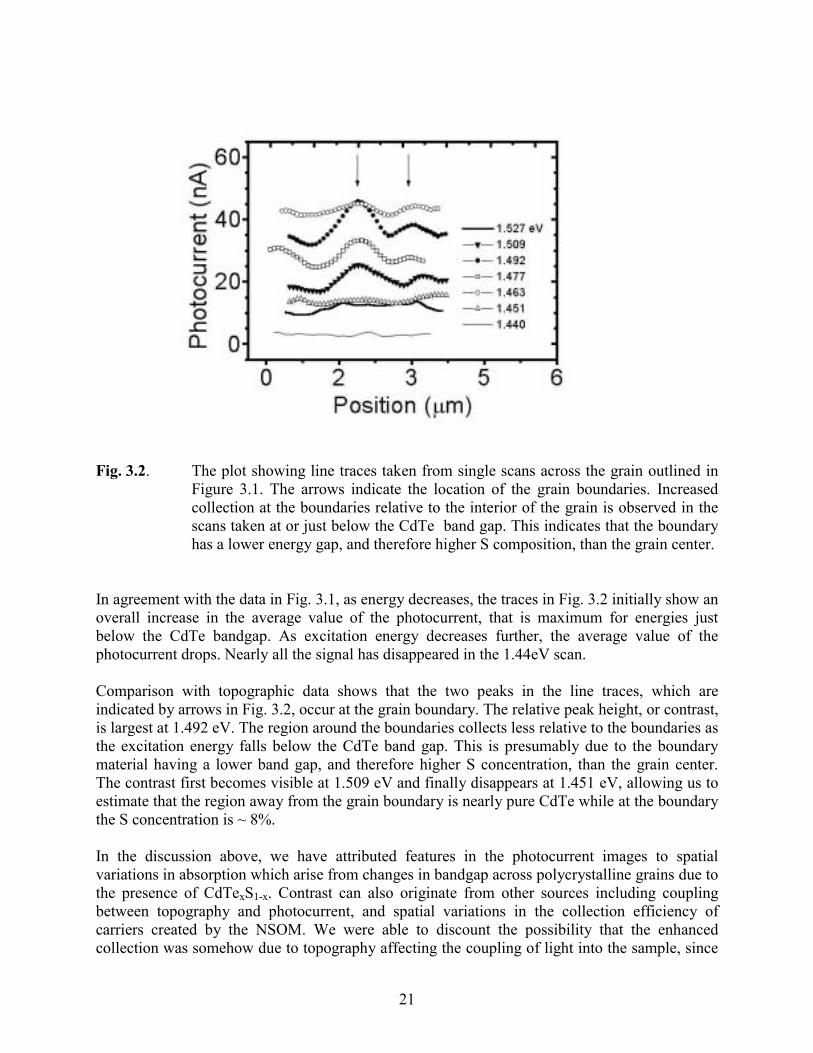
For excitation energies below the CdTe band gap, a large amount of contrast was visible acrossthe photocurrent images. For example, localized regions of higher photocurrent are visible nearthe interface in both Figs. 3.1(c) and 3.1(d). Presumably this contrast arises from variation in Scontent and hence bandgap across these regions. A particularly interesting example of thiscontrast is seen in Fig. 3.1(c) where a loop of higher photocurrent is clearly visible within theoutlined region. This correlates exactly with the boundary of the grain identified in Fig. 3.1(a).To clarify the energy dependence of this feature, a series of measurements across this grainwas recorded while varying the excitation energy from 30meV above to 60meV below theCdTe band gap. The results are shown in Fig. 3.2 where each line on the graph representsa single horizontal scan across the grain. Each scan was made at the same location usinga different excitation energy.

20
Fig. 3.1. Topography (a) and photocurrent (b-d) NSOM measurements taken on the crosssection of a CdS/CdTe solar cell. The same grain has been outlined in thetopography and in each of the photocurrent images. The shift in its position is dueto drift which was tracked using the topographic images. (b) The excitationenergy of 1.615eV is above the CdTe bandgap. (c) The excitation energy of1.463eV is ~50 meV below the CdTe bandgap. Increased width of the collectionregion in the CdTe layer is observed compared to (b). For the marked grain, thecollection is much greater at the boundary than in the interior. (d) The excitationenergy is 1.422eV.
21
Fig. 3.2. The plot showing line traces taken from single scans across the grain outlined inFigure 3.1. The arrows indicate the location of the grain boundaries. Increasedcollection at the boundaries relative to the interior of the grain is observed in thescans taken at or just below the CdTe band gap. This indicates that the boundaryhas a lower energy gap, and therefore higher S composition, than the grain center.
In agreement with the data in Fig. 3.1, as energy decreases, the traces in Fig. 3.2 initially show anoverall increase in the average value of the photocurrent, that is maximum for energies justbelow the CdTe bandgap. As excitation energy decreases further, the average value of thephotocurrent drops. Nearly all the signal has disappeared in the 1.44eV scan.
Comparison with topographic data shows that the two peaks in the line traces, which areindicated by arrows in Fig. 3.2, occur at the grain boundary. The relative peak height, or contrast,is largest at 1.492 eV. The region around the boundaries collects less relative to the boundaries asthe excitation energy falls below the CdTe band gap. This is presumably due to the boundarymaterial having a lower band gap, and therefore higher S concentration, than the grain center.The contrast first becomes visible at 1.509 eV and finally disappears at 1.451 eV, allowing us toestimate that the region away from the grain boundary is nearly pure CdTe while at the boundarythe S concentration is ~ 8%.
In the discussion above, we have attributed features in the photocurrent images to spatialvariations in absorption which arise from changes in bandgap across polycrystalline grains due tothe presence of CdTexS1-x. Contrast can also originate from other sources including couplingbetween topography and photocurrent, and spatial variations in the collection efficiency ofcarriers created by the NSOM. We were able to discount the possibility that the enhancedcollection was somehow due to topography affecting the coupling of light into the sample, since

22
many such grain boundaries did not show a significant variation in photocurrent. This can beseen in Fig. 3.1 where several grain boundaries visible in the topography do not show largephotocurrent contrast. Our tests also showed that the enhanced contrast at the boundaries wasindependent of such measurement parameters as probe-sample separation, illumination intensity,and scan speed.
The presence of spatial variations in the efficiency with which carriers are collected is a moreinteresting possibility to consider. For the photocurrent measurements shown in Figs. 3.1 and3.2, small changes in excitation energy dramatically affect the spatial nonuniformities observed.This leads us to conclude that they are not due to variations in collection efficiency, as we wouldexpect such variations to be observable over a broader range of wavelengths. In some crosssectional photocurrent images of these devices we have, however, observed enhancements inphotocurrent near grain boundaries which are present not only at energies below the CdTebandgap but also well above the bandgap, and which we believe are due to enhanced collectionefficiency near the grain boundary. Probably, this effect is not due to (or not only to) thepresence of the ternary phase at the GB region. In any case the effect deserves to be studiedmore thoroughly.
3.4 Conclusions
Experimental results presented in this report demonstrate the effectiveness of NSOM as ahigh resolution method for studies and two dimensional mapping of current collection overthe cell cross section.
Variation of excitation wavelength from above to below CdTe bandgap provide new optionsfor correlating specific topographic features of carrier photogeneration and current collectionin polycrystalline thin film solar cells.
The S concentration across annealed CdTe/CdS heterojunctions is quite nonuniform. Wewere able to directly observe regions at grain boundaries which have a lower band gap thanthat at grain centers, indicating a higher S content at the boundary. This provides very strongevidence that S diffuses preferentially along the grain boundaries of polycrystalline CdTe andsuggests that the overall lack of uniformity in S composition is a result of this grain boundaryassisted diffusion mechanism.
In some cross sectional photocurrent images, enhancements were observed in photocurrentnear grain boundaries which are present from energies well above the CdTe bandgap tobelow the gap and which we believe are due to enhanced collection efficiency near the grainboundary. This result is of a significant importance if verified by future studies. Explorationof transport effects near grain boundaries in more detail hopefully can clarify mechanisms ofgrain boundary effect on cell performance.
We thankfully acknowledge support from the National Science Foundation under GrantNo. DMR-9704780.

23
4. Impedance Spectroscopy of CdTe Thin Films
4.1 Introduction
Measurements of the complex impedance on polycrystalline films in a wide frequency range(impedance spectroscopy) are aimed at studies of electronic properties of grain boundaries (GB).They represent a technical approach to the problem of polycrystallinity different from that usedin the previous section. While NSOM is a high spatial resolution technique that allows testingproperties of individual grains and GBs, the impedance spectroscopy measurements characterizeproperties of a film as a whole. Then, based on some physical and electrical models we extractfrom these measurements the parameters averaged over numerous grain boundaries in a sample.The validity of the models used must always be considered. We need to analyze conditions underwhich the particular models are valid or at least provide reasonably small errors in the parameterestimates derived from the measurements.
In this section we present and discuss: physical and electrical models we use; issues related to the experimental techniques and procedures; some results obtained on differently processed CdTe thin films.
4.2 Physical and Electrical Models
The basic idea of the method is that a polycrystalline film consists of two phases with very distinctelectrical properties. One phase is the intragrain (IG) material and the other is represented by the GBregions with the potential barriers for the majority carriers. GB is characterized by high resistanceand also by capacitance provided by depleted semi-insulating layers adjacent to the GB. The grain isassumed to be electrically equivalent to a resistor, RIG, whereas the GB is electrically modeled as aresistor, RGB, in parallel with a capacitor, CGB, see Fig. 4.1.
RGB RIG
CGB
Fig.4.1 The simplest electrical model of a polycrystalline film.Resistor RGB and capacitorCGB represent grain boundary. Resistor RIG represents the intragrain material.
At low frequencies the film impedance is almost totally defined by the GB resistance. At highfrequencies the GB capacitor effectively shunts the GB resistor, so that the measured resistancetends to the IG resistance. Thus measurements in a wide frequency range provide an opportunity

24
to separate individual contributions of GB and IG material to the sample resistance anddetermine the GB capacitance.
The LCR meter can display the results of measurements in various modes. We use most commonlythe p-mode which suggests the tested circuit composed of a resistor and capacitor in parallel, andthe s-mode which suggests the circuit composed of a resistor and capacitor in series. Thus weanalyze simultaneously the measured frequency dependencies of Rp, Cp, Rs and Cs. For the filmmodel in Fig. 4.1, the relations between the displayed Rp, Cp, Rs and Cs values, and the sampleparameters, RGB, CGB, and RIG are as follows:
Rp=RIG+[RGB/(1+α)]·1+α/[1+(RIG/RGB)(1+α)] (4.1)
Rs=RIG+RGB/(1+α) (4.2)
Cp=CGB·(1+α)/[1+RIG/RGB(1+α)]2+α (4.3)
Cs=C·(1+α)/α (4.4)
where α=(RGBCGBω)2 and ω is the angular frequency.
Fig. 4.2 shows that the dependencies calculated with Eqs. 4.1 4.4 fit good measured frequencydependencies of Rp and Rs. Good fitting was also demonstrated for Cp and Cs. In reality, theequivalent circuit of any polycrystalline sample should consist of numerous blocks like that at Fig.4.1 connected in parallel and in series. Good fitting means that using a single block model andlumped parameters is an acceptable procedure for these measurements, and a single block mayrepresent adequately a polycrystalline sample composed of a lot of grains. The fitted results make itpossible to extract lumped parameters, RGB, CGB and RIG from the measurements. Incorporatingmore than one block yielded even better fits, which gives a simple means for evaluating the range ofdistribution of these parameters. Very good fitting was found when three blocks were incorporatedwith the same CGB and RIG values while RGB values for the three blocks related to each other as1:1.5:2. Since resistance of the GB depends exponentially on the barrier height, it may be concludedthat standard deviation of the latter from the average is very small.
The method was recently proved to be effective for studies of grain boundaries in CdTe and CdSthin films on insulating substrates [31, 7, 8, 32]. But it should be mentioned that application of themethod is limited to the films with high resistance grain boundaries. As seen from Eqs. 4.1 and 4.2,an effective shunting of the resistor RGB by the capacitor CGB takes place under condition:α=(RGBCGBω)2>1, that is when the characteristic frequency ωGB=(RGBCGB)-1 is smaller than thetesting voltage frequency, ω.
In general, the real physical and hence electrical models should be more complex than thoseconsidered above. For example, as seen from the data in Sec. 2, the grain bulk contains deep trapsthat contribute to the capacitance measured on the cells (oscillating capacitance). In general, thesetraps also may contribute to the capacitance of the films on the insulating substrates that we studywith the impedance spectroscopy. This oscillating capacitance is connected in parallel to theIG resistance and may shunt it, leading to underestimation of RIG and overestimation of theGB capacitance.

25
Fig. 4.2 Experimental results for the resistance of a CdTe layerdemonstrating the fit to a simple one-block equivalent circuit
Fig. 4.3 presents the electrical model for this case. For the films we have studied so far, RIG<<RGB,and, according to our estimates, CIG does not exceed significantly CGB. That means that at not toohigh frequencies the total measured impedance is dominated by grain boundaries. Only in the rangeof frequency above 10 MHz we could see some small deviations of the measured parameters fromthose calculated with equations 4.1-4.4 that might be attributed to the influence of CIG. It could bethought that our pervious estimates of RIG based on the simple model (Fig. 4.1) are not too accurate.As to the GB parameters obtained by fitting experimental and calculated data in the frequency rangebelow 5-10 MHz, we believe they are reliable.
Recently we measured undoped CdTe films on bare glass substrates that demonstrate the Hallconcentration of holes at room temperature near 1011cm-3 and Hall mobility in a range of 5-20cm2/Vs. The latter value indicates that the GB resistance is not high, probably being comparable tothe IG resistance. For films of this kind we will have to use the model of Fig. 4.3 to analyze theimpedance spectroscopy data. It is unclear as yet whether we will be able to separate and estimateaccurately the GB and IG resistance and capacitance.
CdTe - serial/parallel resistance
1.E+02
1.E+03
1.E+04
1.E+05
1.E+06
1.E+07
1.E+08
0.0001 0.001 0.01 0.1 1 10 100 1000
Frequency (MHz)
Res
ista
nce
(Ohm
)
Rp(meas)Rs(meas)Rp(calc)Rs(calc)

26
Fig. 4.3 Electrical model that includes capacitance of the intragrain material.
We have also found [32, 8] that the measured capacitance changes with the bias applied to thesample. As bias deviates from zero, capacitance increases and tends to saturation, and thendecreases as bias voltage increases further. The bias-dependent resistance and capacitance wereobserved previously on a variety of semiconductors containing grain boundaries, e.g. on Si [33],Ge [34], GaAs [35] and CdTe bicrystals [6], and ZnO varistors [36]. The non-linearity of the DCresistance was explained and modeled in [37] based on the idea that under high enough bias theelectrical charge trapped by the GB states and the GB potential barrier height increase. This inturn should lead to increase in the GB depletion width and reduce of the measured depletioncapacitance. This effect was observed and discussed in [6, 35].
However a significant increase under bias applied was observed in the low-frequency range on Sibicrystals [38]. This effect was attributed to the carrier transfer between the grain and the GBtraps which is out of phase with the oscillating testing voltage. Thus the total AC current is a sumof grain-to-grain and grain-to-GB currents. Accordingly, the electrical model of a grain boundaryshould be modified (see Fig. 4.4). The out-of-phase grain-to-GB carrier transport can be modeledwith a capacitor CT in series with a resistor RT, which represents a finite probability for carriersincident on the GB to be trapped. The product RTCT≡τT=1/ωT is the characteristic time of a trap(reciprocal of the characteristic frequency ωT) and is related to the emission rate. The in-phaseand out-of-phase grain-to-grain transports are modeled with a resistor RG-G and a capacitor CG-G.Capacitors CT and CG-G represent the oscillating and depletion capacitances of the GB,respectively.
RG-G
CG-G
RIG
RT CT
Fig. 4.4. Modified electrical model for the polycrystalline film. RG-G and CG-G relate to thegrain-to-grain electrical transport, RT and CT to the grain-to-GB transport; RIGrepresents resistance of the intragrain material.
RGB RIG
CGB CIG

27
When fitting our AC measurements of CdTe films with this electrical model, it was found thatRIG is orders of magnitude smaller than RG-G and RT. Its variation in reasonable limits does notinfluence the fitting value of capacitance, at least in the frequency range of f<5MHz. If weneglect RIG, the capacitance value measured in p mode is described by equation:
Cp=CG-G+CT/[1+(RTCTω)2]= CG-G+CT/[1+(ω/ωT)2] (4.5)
It is seen that for the given RT and CT values, the contribution of the oscillating component to thetotal measured capacitance decreases as the frequency increases, which allows us to separateCG-G and CT. This result is in agreement with our experimental data and also consistent withobservations and discussion in [38,39]. The contribution of CT also decreases with increase in RT(decrease in ωT). It was found that illumination of the sample diminishes RT which makes thecapacitance dependence on bias voltage more pronounced and easier to measure.
4.3 Experimental Technical Problems of Measurement.
4.3.1 Samples for AC characterization.
The samples for measurement are semiconductor films on insulating substrates such as glass.The sample impedance is measured in plane with a two-electrode method. Parallel metal stripsare evaporated on the surface of the semiconductor film through the mask. To provide semi-ohmic low-resistance contacts we evaporate gold on CdTe and aluminum on CdS. DC J-Vcharacteristics measured are linear, indicating ohmic contacts. On the surface of each sample wenormally evaporate six metal strips for the reasons discussed below.
LCR meters have limitations on the resistance of the tested sample. A Hewlett-Packard LCRmeter, Model 4285, we have been using so far, is capable to measure and display the results ifthe sample resistance (real part of the impedance) does not exceed ~50 MΩ. The DC sheetresistance of the CdTe and CdS films we have measured varied in a wide range up to tens andhundreds GΩ. With increasing frequency the real part of impedance reduces (see Eqs. 4.1 and4.2) and becomes measurable at some high enough frequency. But this narrows the frequencyrange we can analyze and make estimates of the film parameters (RGB, CGB, etc.) less accurateand reliable. To decrease the sample resistance, that is the film resistance between twoneighboring metal strips, we use the geometry factor. The mask we use provides the distancebetween metal electrodes of 0.18mm, while the sample width (the size perpendicular to thecurrent direction) is usually of 20 mm. This geometry reduced the sample resistance by morethan two orders of magnitude as compared to the square-shaped sample. By depositing severalstrips on the semiconductor surface, we produce several identical samples, e.g., five samplesbetween six metal strips. When connecting the samples in parallel, we decrease the resistance bya factor of five.
Parallel connection of the individual samples increases the capacitance to be measured. This isan additional advantage of multiple metal strips. The single sample capacitance is rather small,usually ~1 pF. For such a small capacitance to be measured, the problem of parasitic capacitanceand inductance becomes important. Even the leads zeroing procedure provided by the LCRmeter does not necessarily ensure exclusion of the parasitic effects. The multi-strip geometry

28
helped us to some extent to estimate possible inaccuracy due to the parasitic elements in themeasurement circuit. First, the capacitance was measured on all the individual samples on thesame film, that is capacitance values between neighboring pares of strips. Then the samemeasurements were performed on the samples connected in parallel. Based on individualcapacitance values we calculated the expected capacitance of two, three, four or five samples inparallel and compared these values with the measured ones. Discrepancy was usually small, nothigher than 5%. We consider this result as some (if not the ultimate) verification of the smallinfluence of parasitic reactant elements. Another way to estimate parasitic effects we used was tomeasure the glass substrate with electrodes but without semiconductor film. It was found that themeasured capacitance (imaginary part of admittance) was by two orders lower than thatmeasured with the semiconductor film.
4.3.2 Measurements in dark and light.
The sample to be characterized is positioned in a metal box whose internal and external surfacesare coated with a black paint. The sample can be illuminated through a glass window in the topcover of the box. We use a white light source for illumination and neutral filters to vary the lightintensity. To provide dark-measurement conditions the box is thoroughly protected from theroom light with a multi-layer dense black cloth.
All the CdTe and CdS polycrystalline films manifest a significant photo-conductivity effect,especially films with very high GB resistance. Even illumination with a light of 0.1 Sun intensityprovides a 1000 fold decrease in measured resistance for some films. Usually a significantdifference is also observed between resistances measured without using a light source but withand without the black cloth. The measured capacitance is also sensitive to the illumination,especially the bias dependent capacitances.
Another issue to be discussed is the kinetics of photo-response. After turning light on, a steadystate resistance value is achieved in a short time not exceeding one or several seconds. Afterswitching the light off, a rapid increase in resistance takes place initially, followed by very slowrestoration of the dark resistance. This process is not a simple exponential decay. Theinstantaneous relaxation time increases with real time of observation, so that we may wait forhours or sometimes days for the total restoration of the dark resistance. Thus the real darkconditions are not achievable in a reasonable time. It is beyond any doubt that thorough studiesof transient effects are of great interest themselves. These studies can shed light on someimportant properties of deep GB electron states. They also might clarify some light-inducedchanges in defects accumulated at the GB region and their spatial distribution. However,influence of transient effects, which are different for different films, should be eliminated asmuch as possible when we are aimed at routine comparative studies of numerous differentlyprocessed and stressed films. In this case we have to give up the dark measurements and confineourselves to the measurements under controllable light conditions. It was found that the 0.1 Sunlight intensity is usually sufficient for these measurements. First, at this light intensity no long-term transient effects in films were observed at room temperature. Then, the film resistanceunder these conditions reduces, making possible the AC measurements in the whole frequencyrange (see. Sec. 4.2.1). At last, but not least, the sample heating by light is small, which is
29
important when studying the GB resistance, which depends exponentially on temperature due tothe GB potential barriers.
4.4 Impedance Spectroscopy Studies of CdTe Films.
Here we present the comparative studies of the films with different post-deposition treatments.These studies are continued and their final results will be presented and discussed in more detaillater. CdTe films on the glass substrates were prepared by B. McCandless at the Institute ofEnergy Conversion (University of Delaware) with physical vapor deposition at a substratetemperature of 325o C. Some films were treated with CdCl2 and doped with S or Cu at the CSMfacilities. AC measurements of Rp, Rs, Cp, and Cs were performed with and withoutillumination. Measurements at zero bias and fitting data with Eqs. 4.1- 4.4 were used to obtainRGB, CGB, and RIG values for each sample.
The RGB value was orders of magnitude greater than the RIG for all films. The estimated potentialbarrier height Φb without illumination varied from 0.7 to 0.3 eV depending on post-depositiontreatment. The decrease in barrier height caused by illumination achieved for some films 0.15-0.2eV. The CdCl2 treatment lowered RGB under illumination only. Sulfur diffusion lowered RGBunder illumination, but increased RGB when in dark. Finally, copper diffusion into CdTe filmswas found to lower RGB both in dark and under illumination by more than two orders ofmagnitude.
As mentioned in Sec. 4.2, the contribution of oscillating capacitance is zero without applicationof bias. Thus capacitance measured at zero bias is equal to the depletion capacitance. Based onthe average grain size and film geometry and assuming the square-shaped grains of the samesize, we estimated the specific GB depletion capacitance CG-G*, that is capacitance per unit areaof a single GB. Its value did not vary much with the varying post deposition treatment and was ina range of around 5x10⁻⁷ F/cm2. The space charge density NGB in the GB depletion region wasestimated from the CG-G* value using the equation:
NGB=(8Φb0/eεεo)(CG-G*)2 (4.6)
where Φb0 is the zero-bias potential barrier height. The obtained value was in the range of1018cm-3. The CG-G*, hence the NGB value might be overestimated by assuming such a simplemorphology of the films but the error could not be orders of magnitude. Thus one can concludethat NGB is much higher than the carrier concentration derived from the C-V measurements onthe CdTe cells. This result is consistent with the estimates obtained in [7] by using essentiallydifferent method. As mentioned in Sec.1.4, in the case of dominating compensation of acceptorsby the GB states, the negative space charge density in the GB proximity, should be close to NAand can be much higher than the free hole concentration derived from the C-V profile. However,one cannot exclude an enhanced doping density in the GB region due to accumulation of dopant.Indeed, the estimated value of NGB for the Cu-doped films was several times higher than that forthe undoped films.
30
As shown in [38], measurements of bias-dependent oscillating capacitance CT can provide anestimate of the GB density of states. In [32] we have presented a simplified analysis of theproblem limited to the case of a low bias applied to a single GB, namely, V*<Φb0/2. For thespecific capacitance we have obtained the equation:
CT*=2CG-G*(0)/[1+4CG-G*(0)/e2NT]× tanh (V*/2kT) (4.7)
where V*=Vbiasd/l, Vbias is the bias voltage applied between probes, l is the inter-probe distance,and d is an average grain size. The density of the GB traps, NT, is assumed constant, because asmall V* effects both the trap occupation and Fermi level position with respect to the trap bandonly slightly.
Thus the measured capacitance increases with bias until it reaches saturation at V*>2kBT, then itmay slowly decrease due to the geometry capacitance. Using this model, and allowing d and NT tobe fitting parameters, one can obtain information about average grain size and GB density ofstates:
NT = (4/e2)× β/(2-β)× CG-G*(0); β= CTsat/CG-G(0) (4.8)
It was found that the measured CT(Vbias) dependence fits the equation above for all the filmsstudied. The estimated density of the GB states, NT, was in the range of 1012 to 1013cm2. For Cu-doped films it was higher than for the undoped ones.
31
5. Studies of Band Spectrum and Electron Scatteringin Transparent Conducting Oxides
5.1 Introduction
To improve the properties of existing and new TCOs, it is important to put the topic on a solidscientific basis by obtaining detailed information about the electronic properties of thin films, aswell as about the effect of substrates (glass, polymer, other semiconductors etc.), film structure,morphology etc. This information, and its theoretical analysis, will enable an estimate to be madeof the limiting mobility and of the achievable figure-of-merit for practical TCOs. The approachrequires a variety of methods and tools for characterization of the fabricated samples as well assolid scientific grounds for interpretation and theoretical analysis of the data.
In our previous Annual Report to NREL [32] we presented studies of band parameters andelectron scattering in SnO2:F thin films. It was shown that worthwhile information and reliablenumerical estimates of the parameters can be obtained by means of optical characterization(ellipsometry), the Hall and Seebeck coefficients measurements. In this report we present atechnique named the four-coefficient (FC) method based on studying electron transportphenomena in stationary external fields. This method is aimed at determination of mobility, thedensity-of-states (DOS) effective mass, md*, and scattering parameter, r (hence the dominatingscattering mechanism) as a function of the carrier concentration/Fermi level position. It is basedon the simultaneous measurements of four transport coefficients: electrical conductivity, σ, theHall, Seebeck, and Nernst-Ettingshausen coefficients, RH, α, and Q, respectively. The methoddoes not require fulfilling the condition of strong magnetic field (µB>>1) as some powerfulmethods (e.g. cyclotron resonance, Shubnikov-de Haas and de Haas- van Alphen effects) for theband structure studies do. This is a significant advantage for TCOs that typically have smallmobilities and do not meet this condition (µ < 100 cm2 V-1 s-1, and µ B <0.01 for B = 1 Tesla).Measurements in a wide range of carrier concentration/Fermi level position provide detection ofnon-parabolicity and establishment of real dependence of the electron energy on the wave vector,E(k). Being combined with measurements of the plasma and collision frequencies (ultra-highfrequency electron transport) the FC method provides guidance about the shape of the constant-energy surfaces in k-space. This combination also allows an elucidation of the influence of thegrain boundaries on electrical properties and, in particular, on the measured film sheet resistanceand bulk resistivity.
The method was first proposed and applied to studies of n-PbTe in [40] and then used widely forstudying a variety of semiconductors and semimetals, in both bulk and thin film form, see, e.g.,[41-43]. In 1995 joint studies by Dr. T. Coutts, NREL and Dr. V. Kaydanov, CSM were started,aimed at applying the method to investigation of TCO materials. It is hard to overestimate thecontribution of W. Mulligan and D. Young to these studies. Both were CSM Ph.D. studentsadvised by T. Coutts and V. Kaydanov. Dr. Mulligan created the first system that providedmeasurements of the four coefficients in typical TCO thin films and performed preliminaryexperiments on cadmium stannate [44]. Dr. Young has developed new, more perfect andsophisticated measurement equipment and performed systematic comparative studies of a varietyof TCO thin polycrystalline film materials [45-48].
32
In section 5.2 we discuss the electronic properties that determine carrier mobility and affect theoptical transmittance. These are primarily the effective mass tensor and the nature of carrierscattering processes. In section 5.3 we describe and ground theoretically the four-coefficientmethod. The next section 5.4 shows what information and in what way could be extracted fromthe comparison the stationary-field and ultra-high frequency (optical) data. Section 5.5 presentsthe major results of the TCO thin film studies by using the methods described in previoussections.
5.2 Electron Parameters to be Determined. Their Influence on the TCO Figure-of-Merit.
5.2.1 Band model, the effective mass tensor, and density of states.
Along with the bandgap that defines the short-wavelength transmission limit of the material,other details of the band structure are necessary to determine the achievable figure-of-merit. Ingeneral, we need to know the dependence of the carrier energy on its wave vector, k, in theconduction band. In particular, we are interested in the shape of the constant-energy surfaces ink-space and the effective mass value, which are equivalent to the dependence E(k). We will limitthe discussion to i) isotropic, spherically-shaped surfaces, ii) single-ellipsoid surfaces, and iii)multi-ellipsoid surfaces. By way of example, we shall consider the conduction band of silicon.
In general, the reciprocal effective mass is a second rank tensor that reduces to a scalar quantityfor a spherical band. For a single-ellipsoid model, it is characterized by three values of effectivemass, mi
∗ (i=1, 2, 3), each corresponding to one of the principal axes of the ellipsoid. In the caseof the ellipsoid of revolution, we have only two independent values of the effective mass: m7*related to the direction of the revolution axis, and m⊥* related to the perpendicular axis. In the n-Si-like band model we have 6 equivalent ellipsoids located in k-space on the <100>-type axeswhich are the axes of revolution.
Together with the relaxation time, τ, which is to the first approximation reversal of the collision(scattering) frequency, effective mass determines mobility. The smaller the effective mass, thehigher the mobility. For the isotropic band, the carrier mobility is determined by the equation
*)(
mEe = τµ (5.1)
in which )(Eτ symbolizes averaging τ over the conduction band weighted for a parabolic
band by E3/2
∂∂
Ef0 where f0(E) is the Fermi-Dirac distribution function. A highly degenerate
electron gas, such as a typical TCO, has EF − Ec( ) / kBT >> 1. EF is Fermi energy, Ec is theenergy of the minimum in the conduction band, and kB is the Boltzmann constant. In such
materials
∂∂
Ef0 differs from zero only in the vicinity of Fermi level, hence only the carriers
with energies close to Fermi level contribute to electron transport. The properties of thesecarriers determine the magnitude of the mobility and the other transport coefficients. Thus for anisotropic band, mobility is given by

33
µ = eτ EF( ) m∗ EF( ). (5.2)
Subsequently, we shall presume high degeneracy, omit the reference to the Fermi level.For an isotropic relaxation time the only reason for the mobility to be anisotropic is anisotropy ofthe effective mass. For a single ellipsoidal band, the mobility may be expressed as
*i
i meτµ = (5.3)
in which the subscript refers to the three principal ellipsoid axes. In polycrystalline material, withrandomly oriented crystallites, averaging spatially leads to an isotropic mobility, given by
==
3
1 *1
31
i imeτµ (5.4)
For crystals of cubic symmetry with multi-valley band, such as n-Si or n-Ge, the mobility isisotropic and may be described by
µ = eτ mc∗ . (5.5)
mc∗ is the conductivity effective mass and is determined by
1mc
∗ =13
1m||
∗ +2
m⊥∗
. (5.6)
The factor of 2 inside the parentheses arises because there is rotational symmetry of the ellipsoidin k-space. The conductivity effective mass influences the plasma frequency and, hence, thelong-wave limit of transparency of the TCO. The plasma frequency is given by
ωp =e2N
mc∗ε∞ε0
1 2
, (5.7)
where N is the carrier concentration, ε0 is the free space dielectric constant, and ε∞ is the highfrequency dielectric permittivity of the material.
The density-of-states (DOS) function, D E( ) is an important characteristic of a material that alsodepends on effective mass. For a parabolic band spectrum ( Eα k2 )
2/13
2/3* )2(4)( E
hm
ED dπ= (5.8)
34
Here m*d is the density-of-states (DOS) effective mass, which is a combination of the effective
mass components. For the cases of an isotropic spectrum, a single ellipsoid band and a multi-ellipsoidal band, the DOS effective mass is given by equations (5.9) a), b) and c), respectively.
** mmd = a)
3/1*3
*2
*1
* )( mmmmd = b) (5.9)
3/1*3
*2
*1
3/2* )( mmmmd Ν= c)
where N is the number of the equivalent ellipsoids, e.g., N=6 for n-Si. It is seen that m*d can differ
significantly from mc∗ , especially for the multi-ellipsoid model. Comparison of these two values,
which may be obtained experimentally, can provide information about the band structure and, inparticular, whether it is single- or multi-valley. It can also reveal information about theanisotropy of the constant-energy ellipsoids i.e. about the ratio β = m|| m⊥ .
In turn the DOS function, hence the effective mass, determines the Fermi level for a specificcarrier concentration:
= *
23/2
283
dF m
hNEπ
(5.10)
The change in the position of the Fermi level as a function of carrier concentration, relative to theconduction band minimum, leads to the Burstein-Moss shift [49], which defines the short-wavelimit for transparency.
Neglecting the difference between the md* and mc* values can impact estimates of the achievablefigure of merit. One must remember that expressions for mobility and plasma frequency includemc*, while expressions for EF and hence for the Burstein-Moss shift include md*.
5.2.2 Carrier scattering, relaxation time, scattering parameter
Carrier scattering leads to a finite mobility value. The higher the scattering (collision) frequency,hence the lower the relaxation time, the lower the mobility. High scattering rate makes less sharpthe plasma reflection edge, thus worsening the transparency spectrum. It also affects absorptionby free carriers. Carriers are scattered by phonons, point defects, like vacancies, interstitials,impurity atoms and ions, etc., by dislocations, by two-dimensional defects like small angleboundaries (dislocation walls) or grain boundaries in a very fine granular structures. While theeffective mass is considered an intrinsic parameter of a material that depends on its composition,the relaxation time is much influenced by the crystal quality that depends on structuralimperfections, hence on the film preparation technique.
35
Relaxation time depends on the carrier energy (this dependence is different for differentscattering mechanisms). In the case of semi-elastic scattering, dependence of scatteringfrequency on energy can be presented in the form:
τ −1 E( )α W E( )D E( ) (5.11)
where D E( ) is the DOS function and W E( ) is the square matrix element of the electronscattering giving the probability of transition from one quantum state to another of the sameenergy. For the most commonly discussed scattering mechanisms, theory shows that, in aparabolic band, W E( ) is a power function of energy and is commonly represented as
W E( )α E− r (5.12)
In a parabolic band, the density of states is given by
D E( )α E1 2 (5.13)
which means that
τ α E r−1 2 (5.14)
The quantity r is known as the scattering parameter and it is different for each scatteringmechanism, varying from r=0 for acoustic phonon scattering, to r=2 for ionized impurityscattering. This kind of dependence, with a fixed value of the scattering parameter, takes placeonly if the same scattering mechanism dominates over the entire energy range. In reality, severalscattering mechanisms may occur simultaneously. The total scattering frequency is the sum ofthe individual frequencies due to each of the scattering mechanisms, which may be expressed as
ωc = τc−1 = τ i
−1
i (5.15)
The dependence of relaxation time on energy can be more complicated when a wide range ofenergies is being considered. Fortunately, in the case of high degeneracy (the only practical casefor TCOs), only a narrow range of energy around EF is of interest. In this case W(E) can beapproximated by a power function
W E( )= W EF( )× E EF( )−r(5.16)
The scattering parameter in this case is defined as
r EF( )=d ln τd ln E
E= E F
+12
(5.17)
Along with the concentration and temperature dependence of mobility, knowledge of thescattering parameter value is important for identifying the dominant scattering mechanism(s).
36
It is also to be noted that relaxation time depends on the effective mass because of its inversedependence on the density of states. In heavily doped (degenerate) TCOs, scattering by impurityions is sometimes the dominant scattering mechanism. In this case, for materials that have thesame carrier concentration, density of impurity ions and dielectric permittivity, there can be adifference in mobility because of different effective masses, τ ∝ 1/m*, thus µ∝1/m*2.
5.2.3 Influence of non-parabolicity
The dependence E(k) is parabolic only in the immediate vicinity of the conduction bandminimum. As energy increases, the dependence deviates from parabolic and the only question isat what energy the deviation becomes sufficiently important to influence the properties ofelectrons of interest. The most obvious indication of non-parabolicity is the increase of measuredeffective mass with energy (with Fermi level or carrier concentration in degeneratesemiconductors). In narrow-gap, direct-gap semiconductors, such as InSb, (Hg,Cd)Te, PbSe,(Pb,Sn)Te, non-parabolicity significantly affects electronic transport properties at Fermi levels ofonly EF ∼ 0.1eV, or even lower. For wide-gap semiconductors, such as TCOs, non-parabolicityhas not been much investigated but for heavily doped ZnO, CdO, and zinc stannate it has beenestablished that there is a progressive increase of the density-of-states effective mass with carrierconcentration [46-48].
To analyze the influence of non-parabolicity, we consider the theory of electron transportdeveloped in [50, 51] for the rather general, multi-ellipsoid, non-parabolic band model. Theequations for the transport coefficients are based on solutions of the Boltzmann equation and therelaxation time approximation.
In [50, 51] the energy dependence on wave vector in the principal ellipsoid axes (1, 2, 3) isdescribed by the equation:
2
2k1
2
m10∗ +
k22
m20∗ +
k32
m30∗
= γ E( ) = E 1+
EE1
+E2
E22 +
E3
E33 + ........
(5.18)
where *0im (i=1, 2, 3) are the effective mass components at the bottom of the band (E=0). γ (E) is
an arbitrary function of energy which may be represented as a power series in energy withcoefficients given by E1, E2
2, E33, etc. The latter have dimensions of energy raised to the same
power as their energy term in each numerator. The values of E1, E2, E3, etc., determine thedeviation of the spectrum from parabolic for each energy E. If E<<E1, E2, E3, etc., the equationreduces to that of a parabolic band. We will refer to first order non-parabolicity as the case when
γ E( )≈ E 1 +EE1
(5.19)
in the energy range of interest, while the terms of higher in energy power can be neglected.
For the non-parabolic spectrum, the equations for the effective masses, density of states functionand carrier concentration are
37
mi∗ E( ) = mi 0
∗ dγdE
a)
mc∗ E( ) = mc0
∗ dγdE
b)
md∗ E( )= md0
∗ dγdE
c)
(5.20)
D E( )=4π 2md 0
∗( )3 2
h3 γ EF( )[ ]1 2 dγdE
(5.21)
N =8π3
2md0∗( )3 2
h3 γ EF( )[ ]3 2(high degeneracy) (5.22)
It is seen that the effective mass increases with energy since dγ dE > 0 . The density of statesgrows more rapidly with energy and Fermi level increases slower with the carrier concentrationthan in a parabolic band.
Non-parabolicity changes the relaxation time dependence on energy. One of the reasons is thechange in the D(E) dependence. The scattering matrix element is preserved in [51] with the samedependence as in the parabolic case, W E( ) ∝ k2( )− r
, with the same values of the scatteringparameter r for each particular scattering mechanism. Thus, based on equation (5.21), oneobtains for the non-parabolic spectrum
( ) ( )[ ]1
2/11−
−−
∝∝dEdEDEW r γγτ (5.23)
instead of 2/1−∝ rEτ for the parabolic band.
The above analysis shows that we need to know the real dependence, E(k), when trying toestimate the limiting value of mobility, µlim, for heavily doped TCOs. Using, for example, theeffective mass obtained from a sample of a not-too-high carrier concentration, one canoverestimate µlim for a material with a more practical carrier concentration. The same is true forthe plasma frequency and the Burstein-Moss shift. Analysis of the transport phenomena, aimedat establishing the dominant scattering mechanism, can lead to the wrong conclusions ifparabolic theory is applied to a material while the spectrum is actually non-parabolic.
5.3 Method of Four Coefficients (Electron Transport in Stationary External Fields).
As mentioned in Sec.5.1 the method discussed in this section is aimed at the determination ofmobility, the DOS effective mass, m*
d , and the scattering parameter, r. It is based on thesimultaneous measurements of four transport coefficients: electrical resistivity, ρ, the Hall,

38
Seebeck, and Nernst-Ettingshausen coefficients, RH, α, and Q, respectively (ρ and α at B=0 andRH and Q in a weak magnetic field).
Hall effect measurements provide the carrier concentration. In a weak magnetic field (µ B << 1),
RH = AR qN , (5.24)
where q = −e for electrons and q = e for holes. The Hall factor, AR, which is isotropic forspherical and single-ellipsoid constant-energy surfaces, is very close to 1 in the case of highdegeneracy. For a multi-ellipsoid band in cubic crystals (like n-Si and n-Ge) it is also isotropicbut its value depends on the anisotropy of the ellipsoids. It is given by
AR =3β β + 2( )
2β +1( )2 , (5.25)
where
β =m||
m⊥
(5.26)
This brings some uncertainty in the determination of N, but fortunately not too high. Forexample, AR=0.96 for β=2, and AR=0.82 for β=10.
Combined measurements of ρ and RH provide an estimate of the mobility. The so-called Hallmobility differs from the real drift mobility by the Hall factor, AR. Hence,
µρµ RH AR == / (5.27)
Combined measurement of Hall coefficient (carrier concentration) and Seebeck coefficient(thermopower) is one of the oldest methods used to estimate the effective mass insemiconductors. For a parabolic band and high degeneracy, the Seebeck coefficient is given by
3/2
*
2
23/5
)1(3
8Nm
rqh
Tk dB +
= ππα (5.28)
Equation (5.28) contains one more quantity to be determined, namely the scattering parameter, r.Using this equation without knowledge of the value of the scattering parameter, can lead to arather inaccurate estimate of m*
d . For example, if one assumes that the dominant scatteringmechanism is due to acoustic phonons, for which r=0, one will obtain a value of m*
d three timesgreater than that obtained if one assumes ionized impurity scattering, for which r=2.
The problem can be solved by measuring the resistivity and the transverse Nernst-Ettingshausen(N-E) coefficient along with the Hall and Seebeck coefficients. The thermo-magnetic N-E effectis defined by the equation [52]:
39
Ey = −Q dTdx
Bz . (5.29)
For a parabolic band and with high degeneracy of the carrier gas, the N-E coefficient can bedescribed by
Q = α µHr −1 2r +1
(5.30)
Combining Eqs. (5.28) and (5.30), one obtains
−
=HB
FdQ
TkehNEm
µα
π 2
23/2
4*
83)( (5.31)
and
r =32
Qα µH − Q
+12
(5.32)
Thus, by measuring the four transport coefficients, one can determine both the DOS effectivemass and scattering parameter. In the non-parabolic case equations (5.28) and (5.30) transformto
[ ]FEd
B rmNqh
Tk)1(1
38 *
3/22
23/5
λππα −+
= (5.33)
and
Q =FE
H rr
−+−−λ
λµα12/1 (5.34)
where
dN
dmmN
dEd
dEdEE d
d
*
*
2
2
2)(2)( =
≡−γγγλ (5.35)
It is easy to show that md∗ can be calculated from the measured data using the same equation
(5.31) as in the parabolic case. The scattering parameter is now defined as
r =32
Qα µH − Q
+12
+ λ (5.36)
To realize all the advantages offered by this method, we must have heavily doped samples of amaterial in a wide range of carrier concentrations/Fermi level positions. Based on measurementsof the four transport coefficients, we are able to obtain the dependence m*
d = f (N).

40
If m*d (N) = const , the deviations from parabolicity are negligible in this range of N and EF, and,
in subsequent analysis, we may reasonably use parabolic band theory. A substantial increase in m*d
with carrier concentration indicates the need to use the more general non-parabolic band theory.Using the experimental dependence m*
d = f (N), with equations (5.20) (5.22), we can reconstructthe function γ (E) and, hence, E(k). The scattering parameter data enable us to identify thedominant scattering mechanism and to monitor its changes as a function of carrier concentration.
It should be mentioned here that the empirically established correlation, α ~ N , can be used tomap the carrier concentration distribution over the sample area of a thin film. Measurement ofthe local Seebeck coefficient, at various positions on the surface, by relocating the thermoprobe,is a non-destructive and simple method that may be applied to films of an arbitrary size andshape.
5.4 Combining the Four-Coefficient Method with Optical Characterization (Ultra-HighFrequency Electron Transport).
5.4.1 Basics of optical method. Conductivity effective mass. Optical mobility
The high electrical conductivity in metals and heavily doped semiconductors, and its dependenceon frequency, significantly influences the optical properties of these materials and, in particular,the transmittance and reflectance spectra. The electrical conductivity is a complex value anddepends on frequency of the electric field. It is given by
σ ω( ) =σ0
1− iωτ(5.37)
where σ0 is the stationary (DC) conductivity, which is defined as
σ0 = e2 Nτ mc∗ (5.38)
The real and imaginary parts of the dielectric permittivity are described by equations:
Re ε = ′ ε = n2 − k2 = ε∞ 1 −ω p
2
ω 2 − ωc2
, 5.39)
and
Im ε = ′ ′ ε = 2nk = ε∞
ω p2ω c
ω ω 2 + ωc2( )
. (5.40)
n and k are the refractive index and extinction coefficient, respectively, ε∞ is the "high-frequency" dielectric permittivity due to the bound electrons. Two characteristic frequencies: ωpand ωc, are totally defined by the free carriers. The plasma frequency, ωp, is related to the carrierconcentration and conductivity effective mass by equation (5.7). The collision frequency, ωc , isthe reciprocal of the relaxation time, ωc=1/τ.
41
When the frequency of an electromagnetic wave, ω, decreases so that it is close to ωp, reflectanceand transmittance of the material change dramatically. If ωc<<ωp, then, to a first approximation,
ε ≈ ′ ε = ε∞ 1− ω p2 ω 2( ) (5.41)
When ε is real and negative (ω <ωp), the solutions to the wave equation decay exponentially inthe material; i.e. no radiation can propagate. Thus at ω = ωp, a sharp increase in reflectivity,known as the "plasma reflectivity edge", should be observed. For real conductors, ωc/ωp isusually not so small, therefore reflectance does not change so rapidly when the frequencyapproaches ωp. The analysis of the measured optical spectra (by, for example, spectrophotometryor ellipsometry) allows the plasma and collision frequencies to be determined.
Based on the plasma frequency and Hall carrier concentration data, it is possible to calculate theconductivity effective mass, m*
c , using equation (5.7). Comparison of m*c with m*
d (see Section5.2.1) provides guidance about the shape of the constant-energy surfaces, and, in particular,enables a distinguishing between the single-valley and multi-valley models. For a single-ellipsoid model this comparison enables an approximate estimation of the deviation from thespherical shape. In principle, measuring dependence m*
c (N) provides establishing of non-parabolicity and reconstruction of γ (E) and E(k) dependencies in the same way as m*
d (N).Coincidence of the obtained results could be considered as an evidence of their reliability, whichis important because each of the methods used separately has in general its own sources of errorsboth technical (like non-accurate measurements, not-to-high uniformity of the samples) andtheoretical (validity of the theories behind the methods).
The empirically established dependence, ω p (N)for a particular material provides an alternativeto the Hall effect method for measuring carrier concentration and its uniformity over the thinfilm area. Multi-angle spectral ellipsometry, with appropriate modeling of the raw data, providesa unique option to test the uniformity of N and µ (via ωp and ωc) over the film thickness [53].
Based on the m*c and ω c data, derived from the optical characterization, one can calculate the
optical mobility defined as
µ0 =eτmc
∗ =e
mc∗ωc
, (5.42)
which is not necessarily the same as the Hall mobility. Comparison of the two provides guidanceabout contribution of the grain boundaries to the measured DC sheet resistance andbulk resistivity.
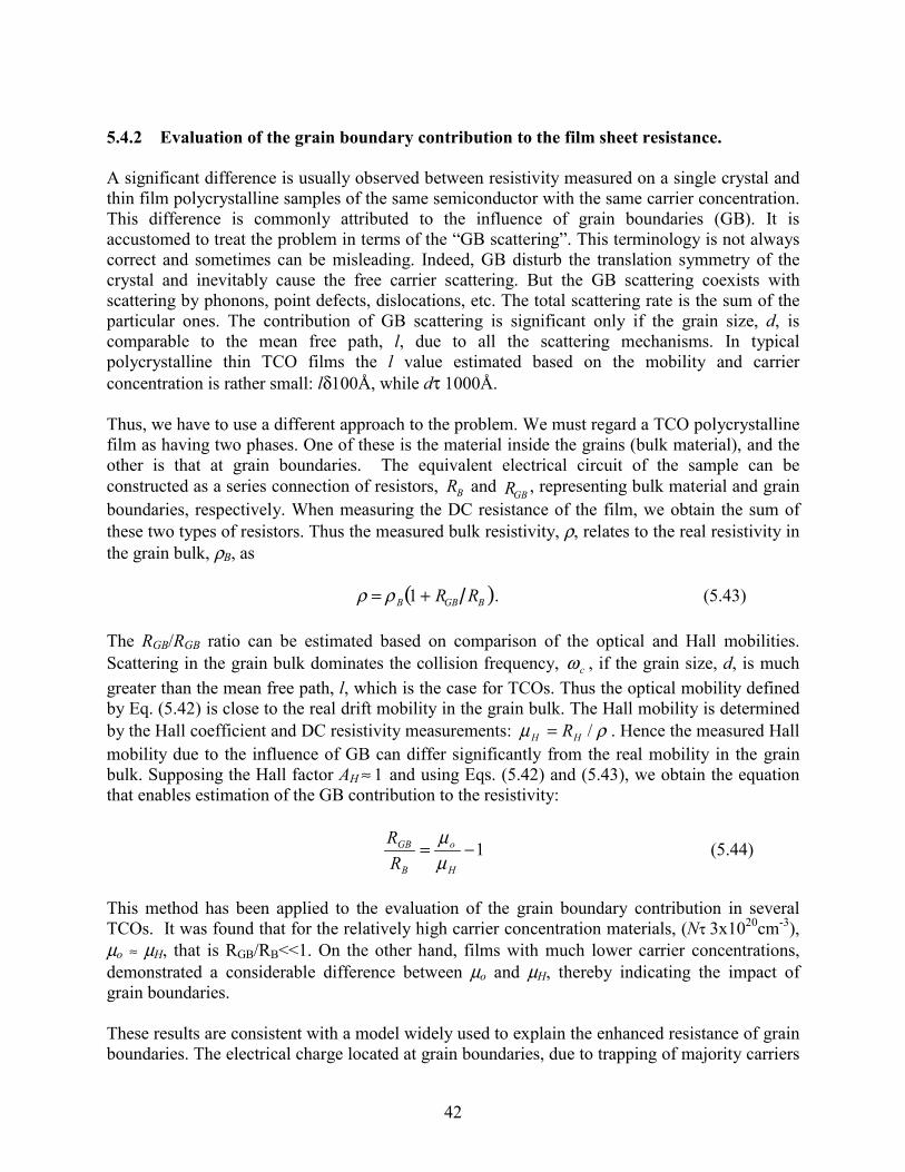
42
5.4.2 Evaluation of the grain boundary contribution to the film sheet resistance.
A significant difference is usually observed between resistivity measured on a single crystal andthin film polycrystalline samples of the same semiconductor with the same carrier concentration.This difference is commonly attributed to the influence of grain boundaries (GB). It isaccustomed to treat the problem in terms of the GB scattering. This terminology is not alwayscorrect and sometimes can be misleading. Indeed, GB disturb the translation symmetry of thecrystal and inevitably cause the free carrier scattering. But the GB scattering coexists withscattering by phonons, point defects, dislocations, etc. The total scattering rate is the sum of theparticular ones. The contribution of GB scattering is significant only if the grain size, d, iscomparable to the mean free path, l, due to all the scattering mechanisms. In typicalpolycrystalline thin TCO films the l value estimated based on the mobility and carrierconcentration is rather small: lδ100Å, while dτ 1000Å.
Thus, we have to use a different approach to the problem. We must regard a TCO polycrystallinefilm as having two phases. One of these is the material inside the grains (bulk material), and theother is that at grain boundaries. The equivalent electrical circuit of the sample can beconstructed as a series connection of resistors, RB and RGB , representing bulk material and grainboundaries, respectively. When measuring the DC resistance of the film, we obtain the sum ofthese two types of resistors. Thus the measured bulk resistivity, ρ, relates to the real resistivity inthe grain bulk, ρB, as
ρ = ρ B 1 + RGB RB( ). (5.43)
The RGB/RGB ratio can be estimated based on comparison of the optical and Hall mobilities.Scattering in the grain bulk dominates the collision frequency, cω , if the grain size, d, is muchgreater than the mean free path, l, which is the case for TCOs. Thus the optical mobility definedby Eq. (5.42) is close to the real drift mobility in the grain bulk. The Hall mobility is determinedby the Hall coefficient and DC resistivity measurements: ρµ /HH R= . Hence the measured Hallmobility due to the influence of GB can differ significantly from the real mobility in the grainbulk. Supposing the Hall factor AH 1≈ and using Eqs. (5.42) and (5.43), we obtain the equationthat enables estimation of the GB contribution to the resistivity:
1−=H
o
B
GB
RR
µµ
(5.44)
This method has been applied to the evaluation of the grain boundary contribution in severalTCOs. It was found that for the relatively high carrier concentration materials, (Nτ 3x1020cm-3),µo ≈ µH, that is RGB/RB<<1. On the other hand, films with much lower carrier concentrations,demonstrated a considerable difference between µo and µH, thereby indicating the impact ofgrain boundaries.
These results are consistent with a model widely used to explain the enhanced resistance of grainboundaries. The electrical charge located at grain boundaries, due to trapping of majority carriers

43
by the electron states, creates a potential barrier for free carriers and increases the resistance ofthe grain boundary regions. With increasing doping level, the amount of the trapped charge alsoincreases, as does the height of the potential barrier. With the further increase in doping level,eventually all the grain boundary states are filled with trapped carriers and the charge cannotincrease any more. However the space charge density in the depletion region continues toincrease causing a reduction in the height and width of the potential barrier, making it transparentto carrier tunneling. Moreover, for a very high doping level, the potential barrier is well belowthe Fermi level and the electrons pass over the barrier without being remarkably perturbed by it[55, 56].
It should be mentioned here that the other method for studying electrical properties of the GBdescribed in Sec. 4, namely Impedance Spectroscopy, is not applicable to the high conductivityTCO films. The limitation is put by the value of the product of the film resistance andcapacitance which defines characteristic frequency of the sample, ωo=(RshCsh)-1. Here Rsh (Ω/)and Csh(F/) are the sheet resistance and sheet capacitance of the film. For the 1 µm thick filmwith a grain size of 1 µm, Rsh ∼ 10 Ω/ and Csh ∼ 0.1 pF/. Thus, ωo ∼ 1012 rad/s = 160 GHzwhich is far beyond the frequency limit of our LCR meters.
5.5 Four Coefficient Measurements.
5.5.1 Measurement techniques and experimental procedure
The four-coefficient instrument created at NREL has already been described and discussed indetail in [45, 47]. Here we present only a brief review of its principal features and operation.
Thin film TCO samples are deposited on electrically insulating substrates and are etchedphotolithographically to the pattern schematically shown in Fig. 5.1b. Two copper blocks withembedded electrical heaters control the sample temperature and the temperature gradient invertical direction when measuring Seebeck and Nernst-Ettingshausen (N-E) effects. The copperblocks have a differential thermocouple mounted between them to measure the temperaturegradient across the sample. One of the blocks has an additional embedded thermocouple forabsolute temperature measurement. The entire sample holder is cooled by a closed-cycle heliumcryostat for temperature-dependent measurements from 30 to 350 K.
Hall effect and resistivity are measured with the van der Pauw method by using electricalcontacts 1, 2, 3, and 4. The Seebeck voltage is measured between contacts 1 and 3, and N-Evoltage is measured between contacts 2 and 4. Note that the temperature gradient is appliedparallel to the short dimension of a sample while the N-E voltage is measured in the longdimension. This geometry of the sample orientation is different from the traditional geometry(see, e.g., [52]) presented schematically at Fig. 5.1a. The latter is similar to the Hall bar geometrywhere current flows along the long side of a sample and Hall voltage is measured along the shortside. The reason for changing geometry is that the N-E coefficient is very small in TCOs. Indeed,this coefficient is proportional to mobility and the ratio kBT/(EF-EC), see Sec.5.3. Bothparameters are small for typical TCOs, so that for the reasonable values of magnetic field andtemperature difference across the sample, the N-E signal is in the nano-volt scale.
44
(a) (b) Sample 1 Substrate
2 4
L 3 dT/dx W Warmer Block Cooler Block EN-E Bz
Fig. 5.1 Comparison of two types of geometry used for the N-E effect measurements.(a) traditional geometry; (b) geometry used in our instrument.
Let us rewrite the equation (5.29) for the N-E effect in terms of temperature difference across asample, ∆T=(dT/dx)L, and the N-E voltage, VN-E=EN-EW, where L and W are the sampledimensions shown in Fig. 5.1a. The new equation is
LWBTQV zEN ××∆×=− (5.45a)
For the geometry shown in Fig. 5.1b this equation transforms to
WLBTQV zEN ××∆×=− (5.45b)
where L and W are the lengths of the long and short sides of a sample respectively. It is see thatrotation of the sample by the angle of 90o with respect to the temperature gradient direction leadsto the (L/W)2 fold increase in the N-E signal. For the real samples we use, L=16 mm andW=3mm, that is (L/W)2=28.4. Thus using the geometry of Fig. 5.1b we provided a significantincrease in the N-E voltage while preserving a reasonably small temperature difference acrossthe sample, of 10 K or less. This geometry was proposed and realized first in [57].
45
5.5.2 Some results and discussion
To demonstrate applicability of the method to studies of TCOs and illustrate typical informationprovided by these measurements, we review here briefly the data obtained for ZnO thin films andpresented in [47].
The films were RF magnetron-sputtered on 7059 glass substrates. The DOS effective mass md* wasstudied with the FC method in the carrier concentration range of 2x10¹⁹ to 5x1020 cm-3. The obtainedvalue of md* varies in this range from 0.3 to 0.45 me indicating non-parabolicity of the conductanceband. The plot of md* vs. N2/3 is linear indicating the first-order non-parabolicity in this concentrationrange. Extrapolation of the plot to N =0, provided mdo*=0.27me (mdo* is the DOS effective mass atthe conduction band bottom). The plasma-frequency conductivity effective mass values for theelectron concentrations of 4x10¹⁹ and 5x1020 cm-3 taken from literature [58, 59] are in a goodagreement with md*. Namely, it regards the deviation from the parabolic spectrum. Besides, thedifference between md* and mc* is rather small which corresponds to the single-valley band inagreement with the theory prediction [60]. The constant-energy shape is close to sphere. Within theaccuracy of measurements the ratio of the ellipsoid principal axes lengths does not exceed 1.5.
The scattering parameter r values were determined as described in Sec. 5.3, using Eq. (5.36) withthe non-parabolicity parameter λ (Eq. (5.35) values derived from the experimental dependencemd
*(N). For heavily doped ZnO:Al samples (N≥4x1020 cm-3) the r value matches well with that forthe impurity ion scattering. For the undoped material (N~2x1019 cm-3), the scattering parameter wasfound to lie closely with the neutral impurity trend.
It is interesting to compare data for ZnO with those for Cd2SnO4 (CTO). CTO films were alsoprepared with the RF magnetron sputtering. Free electron concentration varied between 2x10²⁰ and6.8x1020 cm-3. The DOS effective mass increases with the carrier concentration, but much slowerthan in ZnO, only by a factor of 1.2 in the concentration range indicated above. The md* value inCTO is smaller than in ZnO, by a factor of 1.8 for N =4x1020 cm-3. Probably this differenceaccounts for mobilities in CTO being nearly 3 times larger than in ZnO. First, mobility is reverselyproportional to effective mass, and second, the lower effective mass, and hence lower density ofstates leads to the reduced scattering rate. Indeed, the estimated relaxation time value for N=4x1020 cm-3 in CTO is ~1.6 times that value for ZnO. It is important to point that comparison of theHall and optical mobilities in both materials differ only slightly indicating no considerable impactof grain boundaries on the film sheet resistance. The same conclusion was made previously in [53,54] about SnO2:F films.
5.6 Conclusions
Based on the data above, as well as on the other presented in [44-48], one can conclude that theFC method is a good experimental technique for studies of TCO films, especially if combinedwith the plasma and collision frequencies measurement. This method can be applied to othermaterials, heavily or slightly doped, both in bulk and thin film form. The equipment built atNREL for measuring the four transport coefficients, demonstrated its high quality and capabilityto characterize materials difficult to measure due to low mobility and high degeneracy, such asTCOs. So much the better it could be used for characterization of materials with morefavorable properties.

46
6. References
1. K. D. Dobson, I. V. Fisher, G. Hodes and D. Cahen, Solar Energy Mater. & Sol. Cells 62,295-325 (2000).
2 J. Tang, D. Mao, T. R. Ohno, V. Kaydanov and J. U. Trefny, Proc. 26th IEEE PVSC, Sept.Oct. 1997, Anaheim, CA, pp 439-442.
3. W. Song, D. Mao, Y. Zhu, J. Tang and J. U. Trefny, Proc. 25th IEEE PVSCP, May 1996,Washington, DC, pp 873-876
4. H.C. Chou, A. Rohatgi, E.W. Thomas, S. Kamra, A.K. Bhat, J. Electrochem. Soc. 142, 254
(1995)5. S.E. Asher, R.C. Reedy, Jr., R. Dhere, T.A. Gessert, M.R. Young, NCPV Progr. Rev.
Meeting 2000, April 2000, Denver, CO, p.275
6. T.P. Thorpe, Jr., A.L. Fahrenbruch, and R.H. Bube, J. Appl. Phys. 60, 3622 (1986)
7. L.M. Woods, D.H. Levi, V. Kaydanov, G.Y. Robinson, R.K. Ahrenkiel, Proc. 2nd WorldConf. on PV Solar Energy Conversion, July 1998, Vienna, Austria, p.1043.
8. A.S. Gilmore, V. Kaydanov, U. Laor, A. Gupta, T.R. Ohno, B. McCandless, NCPV Progr.Rev. Meeting 2000, April 2000, Denver, CO, p.259.
9. E.Kucys, J. Jernot, K. Bertulis, and V. Bariss, Phys. Stat. Sol.A 59, 91 (1980).
10. G. Zoth, F.G. Reidel, W. Schroter, Phys. Stat. Sol. B 172, 187 (1992).
11. F. Abou-Elfotouh, S. Ashour, S.A. Alkuhaimi, J. Zhang, D.J. Dunlavy, L.L. Kazmersky,Mat. Res. Soc. Symp. Proc. 238, 335, (1992).
12. A. Castaldini, A. Cavalinu, B. Fraboni, P. Fernandez, J. Piqueras, J. Appl. Phys. 83,2121 (1998).
13. D. Mao, L. H. Feng, Y. Zhu, J. Tang, W. Song, R. Collins, D. L. Williamson, and J. U.Trefny, 13th NREL PV Program Review Proc., AIP Conference Proc. 353, p.352 (1996).
14. M. H. Aslan, W. Song, J. Tang, D. Mao, R. T. Collins, D. H. Levi, R. K. Ahrenkiel, S. C.Lindstrom, and M. B. Johnson, Mat. Res. Soc. Symp. Proc., 485 p.203 (1998).
15. H.C. Chou, A. Rohatgi, N.M. Jokerst, E.W. Thomas, S. Kamra, J. Electron. Mater.25, 1093 (1996).
16. P. Blood and J.W Orton, The Electrical Characterization of Semiconductors: MajorityCarriers and Electron States, Academic Press, 1992.

47
17. Ahmet Balcioglu, Characterization of Deep Impurity Levels in Semiconductor Devices,Ph.D. Thesis, Department of Physics, Colorado School of Mines, Golden, CO, 2000.
18. A. Balcioglu, R.K. Ahrenkiel and F. Hasoon (submitted for publication to J.Appl. Phys.,2000).
19. S.S. Ou, A. Bindal, O.M. Stafsudd, and K.L. Wang, J. Appl. Phys. 55, 1020 (1984).
20. M.A. Lourenco, Y.K. Yew, K.P. Homewood, K. Durose, H. Richter, and D. Bonnet, J. Appl.Phys. 82, 1423 (1997).
21. M.A. Lourenco, W.L. Ng, K.P. Homewood, and K. Durose, Appl. Phys. Lett. 75, 277 (1999).
22. K. Zanio, Semiconductors and Semimetals, Volume 13, Academic Press, 1978.
23. A.J. De Nobel, Phil. Re. Rep. 14, 430 (1959).
24. D.G. Jensen, B.E. McCandless and R.W. Birkmire, Proc. 25th IEEE PVSC, Washington, DC,May 1996, p. 773.
25. G.A. Valaskovic, M. Holton and G.H. Morrison, Applied Optics 34, 1215 (1995).
26. E. Betzig, P.L. Finn and J.S. Weiner, Appl. Phys. Lett. 60, 2484 (1992).
27. K. Ohata, J. Saraie and T. Tanaka, Jap. J. Appl. Phys. 12, 1641 (1973).
28. D.S. Albin, private communication.
29. O. deMelo, M.Melendez-Lira, I. Hernandez-Calderon, L. Banos, and A. Morales-Acevedo,Proc. 1st IEEE World Conf. on Photovoltaic Solar Energy Conversion, New York,1994,p.369.
30. M.S. Unlu, B.B. Goldberg, W.D. Herzog, D. Sun and E. Towe, Appl. Phys. Lett. 67, 1862(1995).
31. J.J.. Kester, S. Albright, V. Kaydanov, R. Ribelin, L.M. Woods, J.A. Philips, NREL/SNL PVProgram Review, Proc 14th Conf., Lakewood, CO, 1996, p. 162.
32. V.I Kaydanov and T.R Ohno, Process Development and Basic Studies of ElectrochemicallyDeposited CdTe-Based Solar Cells, Colorado School of Mines, Annual Technical Report toNREL, Subcontract No. XAK-8-17619-28, Phase I, 15 May 1998-14 May 1999.
33.Y. Matukura, Jpn. J. Appl. Phys. 2, 91 (1963).
34. W.E. Taylor, N.H. Odell, and H.Y. Fan, Phys. Rev. 88, 867 (1952);R. Stratton, Proc. Phys. Soc., London, B 69, 513 (1956).
48
35. M.G. Spencer, W.J. Schaff and D.K. Wagner, J. Appl. Phys. 54, 1429 (1983)
36. M. Matsuoka, Jpn. J. Appl. Phys. 10, 736, (1971);L.M. Levinson and H.R. Philipp, J. Appl. Phys. 46, 1332(1975).
37. G.E. Pike and C.H Seager, J.Appl. Phys. 50, 3414 (1979).
38. C.H. Seager and G.E. Pike, Appl. Phys. Lett. 37, 747 (1980).
39. G.E. Pike, Grain Boundaries in Semiconductors, Elsevier Science Publ. Co., Inc., 1982,p. 369.
40. M.K. Zhitinskaya, V.I. Kaidanov, and I.A. Chernik, Sov. Phys. Solid State 8, 295 (1966).
41. I.A. Chernik, V.I. Kaidanov, E.P. Ishutinov, Sov. Phys. Semicond. 2, 825, (1969).
42. I.A. Chernik, V.I. Kaidanov, M.I. Vinogradova, and N.V. Kolomoets, Soviet Physics-Semiconductors 2, No.6, pp. 645-651 (1969).
43. T.S. Gudkin, V.I. Kaidanov, et.al., Sov. Phys. Semicond. 5, 1089 (1971).
44. W.P. Mulligan, A Study of the Fundamental Limits to Electron Mobility in CadmiumStannate Thin Films, Ph. D. Thesis, Department of Physics, Colorado School of Mines,Golden, CO, 1997.
45. D.L. Young, T.J. Coutts, V.I. Kaydanov, Rev. of Sci. Instr. 71, 462 (2000).
46. T.J. Coutts, D.L. Young and X. Li, MRS Bulletin, 25, No.8, 58 (Aug. 2000).
47. D.L. Young, T.J. Coutts, V.I. Kaydanov, W.P. Mulligan, to be published in J. Vac. Sci.Technol. A 18, No. 6, Nov-Dec. 2000.
48. D.L. Young, A Fundamental Study of Electron Transport in Zinc Stannate Thin Films,Ph.D Thesis, Department of Physics, Colorado School of Mines, Golden, CO, 2000.
49. E. Burstein, Phys. Rev. 93, 632 (1954).
50. J. Kolodziejchak and S. Zhukotynski, Phys. Status Solidi 5, 145 (1964).
51. W. Zawadski and J. Kolodziejchak , Phys. Status Solidi 6, 419 (1964).
52. E. Putley, The Hall Effect and Related Phenomena, Butterworths, London, 1960.
53. A. M. Alkaoud, APCVD Preparation and Studies of Physical Properties of Tin Oxide ThinFilms, Ph. D. thesis, Department of Physics, Colorado School of Mines, Golden, CO, 1999.

49
54. A. Al-Kaoud, T. Wen, A. Gilmore, V. Kaydanov, T.R Ohno, C. Wolden, L. Feng, J. Xi,NCPV Progr. Rev., Proc. 15th Conf., Denver, CO, 1998, p.212.
55. T.S Gudkin, I.A. Drabkin, V.I. Kaidanov, O.G. Sterlyadkina, Sov. Phys. Semicond. 8, 1453(1975).
56. L.I. Bytenskii, S.A. Kazmin, V.I. Kaidanov, Yu.I. Ravich, and A.V. Savelev, Sov. Phys.Semicond. 16, 712 (1982).
57. V.I. Kaidanov and I.A. Chernik, Sov. Phys. Semicond. 1, 1159 (1967).
58. S. Brehme, F. Fenske, W. Fuhs, E. Nebauer, M Poschenrieder, B. Selle, and I. Sieber, ThinSolid Films 342, 167 (1999).
59. K.H. Hellwege, Landolt-Bornstein numerical data and functional relationships in scienceand technology: Semiconductors, in Numerical Data and Functional Relationships inScience and Technology, edited by O. Madelung, M. Scultz, and H. Weiss (Springer, Berlin,1982), vol. 17.
60. S. Bloom and I. Ortenburger, Phys. Status Solidi B 58, 561 (1973).
50
7. Acknowledgements
Many people, in addition to those at the Colorado School of Mines, have contributed to thiswork over the past year. We are thankful to Rick Powell, Doug Rose, Victor Karpov, Don Grecu,and Upali Jayamaha of First Solar, LCC., for supplying us with the materials for CdTe/CdS cellspreparation and for thin film studies. It is hard to underestimate the value of discussions of ourresearch approach and results that we have had with the individuals mentioned above and alsoBolko von Roedern, Tim Gessert, Dave Albin, Peter Meyers, and other scientists involved infabrication and studies of thin film solar cells. We greatly appreciate the encouraging interest inour activities, discussions and suggestions we get constantly from Kenneth Zweibel, Harin Ullal,and especially from our contract monitor, Bolko von Roedern.
8. Appendices8.1 Personnel
The names, titles, and representative responsibilities of the individuals contributed to this work aresummarized below.
Timothy R. Ohno, Associate Professor of Physics: Photovoltaic Development, Surface Physics,Principal Investigator
Victor I. Kaydanov, Research Professor of Physics: Photovoltaic Development, ElectronTransport Phenomena, Principal Investigator
Reuben T. Collins, Professor of Physics: Electronic and Optical Properties of Semiconductors
Don L. Williamson, Professor of Physics: Structural Properties of Materials, XRD
Thomas E. Furtak, Professor of Physics: Optical Properties of Semiconductors, Ellipsometry
Dr. Timothy J. Coutts (NREL): Electronic and Optical Properties of Semiconductor
Materials and devices
Dr. Richard K. Ahrenkiel (NREL), Adjunct Professor of Physics: Electronic and Optical Properties
of Semiconductor Materials and Devices
Dr. Dean H. Levi (NREL): Electronic and Optical Properties of Semiconductor
Materials and Devices
Dr. Akhlesh Gupta, Post. Doc.: CdTe Cell Processing and Characterization
Angelo S. Gilmore, Graduate Research Assistant: Impedance Spectroscopy, Hall effect
Scott Townsend, Graduate Research Assistant: ZnTe Back Contact, Cell Stability
Mary K. Herndon, Graduate Research Assistant: Near Field Scanning Optical Microscopy
(defended Ph.D. thesis November 1999)
Ahmed Balcioglu, Graduate Student: Deep Level Transient Spectroscopy
(defended Ph.D. thesis August 2000)

51
David L. Young, Graduate Student: Electron Transport Phenomena in Semiconductors
(defended Ph. D. thesis August 2000)
Brian Egaas, Graduate Research Assistant: Thin Film Solar Cell Fabrication
Wendi Batchelor, Graduate Research Assistant: Thin Film Solar Cell Fabrication
Don Robb Sparks, undergraduate student, degradation chamber design
8.2 Laboratory Improvements
Some laboratory improvements occurred during Phase II of this subcontract that have permittedmore thorough materials characterization.
A Hewlett-Packard LCR meter, Model 4284A (20 Hz - 1 MHz) was added to the H-P LCR meter,Model 4285A (75 kHz-30 MHz) we possessed previously. Broadening of the frequency rangeprovides more opportunities for studying electronic properties thin films and solar cells using theimpedance spectroscopy method.
Building of the near field scanning optical microscope was completed, which enabled studying andmapping optical and electronic properties of the cell with the spatial resolution of ~100 nm.
52
8.3 Publications/Presentations
1. D.L. Young, T.J. Coutts, V. I. Kaydanov, Density-of-states effective mass and scatteringparameter measurements by transport phenomena in thin films, Rev. of Sci. Instr. 71, pp.462-466 (2000).
2 A.S. Gilmore, V. Kaydanov, U. Laor, A. Gupta, T.R. Ohno, B. McCandless, ACCharacterization of Grain Boundary Electronic Properties in CdTe Thin Films, NCPVProgram Review Meeting 2000, April 2000, Denver, CO, pp 259-260.
3. A.Gupta, S. Townsend, V. Kaydanov and T.R. Ohno, Comparison of Degradation in VaporTransport- and Electro-Deposited CdTe Solar Cells with ZnTe:Cu/Au and Cu/Au BackContacts, Ibid, pp. 271-272
4*. T.R. Ohno, "Photovoltaic Research at the Colorado School of Mines", Physics DepartmentColloquium, University of Colorado-Colorado Springs, October 22, 1999.
5*. A.Gupta, S. Townsend, T. Ohno, V. Kaydanov, Degradation of CdS/CdTe Solar Cells:Cu:ZnTe/Au vs. Cu/Au Back Contact, Electrodeposited CdTe vs. First Solar CdTe,National CdTe R&D Team Meeting, NREL, Golden, CO, January 27-28, 2000.
6*. T. Ohno, V. Kaydanov, R. Collins, A. Gupta, M. Herndon, U. Laor, Grain BoundaryProperties: Observations at the Colorado School of Mines, Ibid.
7*. V. Kaydanov, P. Meyers, Some Possible Effects of Grain Boundaries on Thin Film CellPerformance, Ibid.
8*. D.L. Young, T.J. Coutts, V.I. Kaydanov, W.R. Mulligan, Direct measurement of Density-of-States Effective Mass and Scattering Parameter in Transparent Conducting Oxides UsingSecond-Order Transport Phenomena, The Amer. Vac. Soc. 46th Int. Symp., Seattle, WA,2000
9*. D.L. Young, T. Coutts, X. Li, J. Keane, V.I. Kaydanov, A.S. Gilmore, Density-of-StatesEffective Mass and Scattering Parameter Measurements on Transparent Conducting Oxidesusing Second-Order transport Phenomena, Mater. Res. Soc. Meeting, Spring 2000

REPORT DOCUMENTATION PAGE Form ApprovedOMB NO. 0704-0188
Public reporting burden for this collection of information is estimated to average 1 hour per response, including the time for reviewing instructions, searching existing data sources,gathering and maintaining the data needed, and completing and reviewing the collection of information. Send comments regarding this burden estimate or any other aspect of thiscollection of information, including suggestions for reducing this burden, to Washington Headquarters Services, Directorate for Information Operations and Reports, 1215 JeffersonDavis Highway, Suite 1204, Arlington, VA 22202-4302, and to the Office of Management and Budget, Paperwork Reduction Project (0704-0188), Washington, DC 20503.
1. AGENCY USE ONLY (Leave blank) 2. REPORT DATEMarch 2001
3. REPORT TYPE AND DATES COVEREDAnnual Technical Report, Phase II16 May 1999 13 May 2000
4. TITLE AND SUBTITLEProcess Development and Basic Studies of Electrochemically Deposited CdTe-BasedSolar Cells; Annual Technical Report, Phase II, 16 May 199913 May 20006. AUTHOR(S)V.I. Kaydanov and T.R. Ohno
5. FUNDING NUMBERSC: XAK-8-17619-28TA: PVP15101
7. PERFORMING ORGANIZATION NAME(S) AND ADDRESS(ES)Colorado School of MinesGolden, Colorado 80401
8. PERFORMING ORGANIZATIONREPORT NUMBER
9. SPONSORING/MONITORING AGENCY NAME(S) AND ADDRESS(ES)National Renewable Energy Laboratory1617 Cole Blvd.Golden, CO 80401-3393
10. SPONSORING/MONITORINGAGENCY REPORT NUMBER
NREL/SR-520-29956
11. SUPPLEMENTARY NOTES
NREL Technical Monitor: Bolko von Roedern12a. DISTRIBUTION/AVAILABILITY STATEMENT
National Technical Information ServiceU.S. Department of Commerce5285 Port Royal RoadSpringfield, VA 22161
12b. DISTRIBUTION CODE
13. ABSTRACT (Maximum 200 words) This project, carried out at the Colorado School of Mines, addresses long-term research anddevelopment issues related to polycrystalline thin-film solar cells. Our general research approach is based on combiningactivities aimed at improving cell performance and stability with activities aimed at increasing our fundamental understandingof the properties of materials making up the cells: CdTe, CdS, multilayer back-contact, and transparent conducting oxide(TCO) from contact. We emphasize the relation between structural and electronic materials properties and variousprocessing procedures, as well as the microscopic mechanisms responsible for the cell performance and its degradation.Section 1 presents studies of degradation under stressing of the cells with differently processed CdTe and different backcontents. Section 2 presents studies of deep traps in the electrodeposited (ED) CdTe cells performed in collaboration atNREL. Section 3 reports studies of the spectral dependencies of photocurrent, and their spatial distribution over the cross-section of the ED CdTe cells were performed using near-field scanning optical microscopy (NSOM). Section 4 discusses theimpedance spectroscopy of CdTe and CdS thin films. Section 5 presents studies of band spectrum and electron scattering intransparent conducting oxides. Appendices present data on personnel involved in the studies, laboratory improvements, andpublications.
15. NUMBER OF PAGES14. SUBJECT TERMSPV; polycrystalline thin-film solar cells; CdTe; CdS; multi-layer back contact;transparent conducting oxide (TCO); dopant compensation; degradation of cells;electromigration and transformation; deep traps; near field scanning opticalmicroscopy; impedance spectroscopy; band spectrum; electron scattering
16. PRICE CODE
17. SECURITY CLASSIFICATIONOF REPORTUnclassified
18. SECURITY CLASSIFICATIONOF THIS PAGEUnclassified
19. SECURITY CLASSIFICATIONOF ABSTRACTUnclassified
20. LIMITATION OF ABSTRACT
UL
NSN 7540-01-280-5500 Standard Form 298 (Rev. 2-89)Prescribed by ANSI Std. Z39-18
298-102