process-variation effect, metal-gate work-function
TRANSCRIPT
IEEE TRANSACTIONS ON ELECTRON DEVICES, VOL. 57, NO. 2, FEBRUARY 2010 437
Process-Variation Effect, Metal-Gate Work-FunctionFluctuation, and Random-Dopant Fluctuation in
Emerging CMOS TechnologiesYiming Li, Member, IEEE, Chih-Hong Hwang, Student Member, IEEE, Tien-Yeh Li, and
Ming-Hung Han, Student Member, IEEE
Abstract—This paper, for the first time, estimates the influencesof the intrinsic-parameter fluctuations consisting of metal-gatework-function fluctuation (WKF), process-variation effect (PVE),and random-dopant fluctuation (RDF) on 16-nm-gate planarmetal–oxide–semiconductor field-effect transistors (MOSFETs)and circuits. The WKF and RDF dominate the threshold-voltagefluctuation (σVth); however, the WKF brings less impact on thegate capacitance and the cutoff frequency due to the screeningeffect of the inversion layer. The fluctuation of timing character-istics depends on the σVth and is therefore proportional to thetrend of σVth. The power fluctuation consisting of the dynamic,short-circuit, and static powers is further investigated. The totalpower fluctuation for the planar MOSFET circuits is 15.2%, whichis substantial in the reliability of circuits and systems. The staticpower is a minor part of the total power; however, its fluctuationis significant because of the serious fluctuation of the leakage cur-rent. For an amplifier circuit, the high-frequency characteristics,the circuit gain, the 3-dB bandwidth, the unity-gain bandwidthpower, and the power-added efficiency are explored consequently.Similar to the trend of the cutoff frequency, the PVE and RDFdominate both the device and circuit characteristic fluctuationsdue to the significant gate-capacitance fluctuations, and the WKFis less important at this simulation scenario. The extensive studyassesses the fluctuations on circuit performance and reliability,which can, in turn, be used to optimize nanoscale MOSFETs andcircuits.
Index Terms—Circuit, coupled device–circuit simulation,emerging device technology, intrinsic-parameter fluctuation,modeling and simulation, nanoscale MOSFET, power fluctuation.
I. INTRODUCTION
THE VARIABILITY of performance and yield in nanoscalecomplementary metal–oxide–semiconductor (CMOS) de-
vices is of great interest and has become crucial for circuitdesign. For state-of-art nanoscale CMOS circuits and systems,the intrinsic device parameter fluctuations that result from
Manuscript received June 3, 2009; revised October 23, 2009. First publishedDecember 28, 2009; current version published January 22, 2010. This workwas supported in part by the National Science Council, Taiwan, under Con-tract NSC-97-2221-E-009-154-MY2 and in part by the Taiwan SemiconductorManufacturing Company, Hsinchu, Taiwan, under Grant 2008-2009. The re-view of this paper was arranged by Editor D. Esseni.
Y. Li is with the Department of Electrical Engineering and the Institute ofCommunication Engineering, National Chiao Tung University, Hsinchu 300,Taiwan, and also with the National Nano Device Laboratories, Hsinchu 300,Taiwan (e-mail: [email protected]).
C.-H. Hwang, T.-Y. Li, and M.-H. Han are with the Institute of Communica-tion Engineering, National Chiao Tung University, Hsinchu 300, Taiwan.
Color versions of one or more of the figures in this paper are available onlineat http://ieeexplore.ieee.org.
Digital Object Identifier 10.1109/TED.2009.2036309
line-edge roughness [1], [2], the granularity of the polysili-con gate [3]–[5], random discrete dopants [6]–[33], and othercauses have substantially affected signal system timing [31],[32] and high-frequency characteristics [33]. Yield analysisand optimization, which take into account the manufacturingtolerances, model uncertainties, fluctuations in process param-eters, and other factors, are known as indispensable compo-nents of the robust circuit-design procedure [34]–[37]. Diverseapproaches have recently been presented to investigate theintrinsic-parameter fluctuations in semiconductor devices [10]–[26] and circuits [27]–[33]. Various suppression technologieshave been proposed [10], [18]–[21], [23], [24], [33]. Amongthese approaches, the high-κ/metal-gate technology is the keyto reduce the intrinsic-parameter fluctuations. However, the useof metal as a gate material introduces a new source of randomvariation due to the dependence of work function on the ori-entation of metal grains. The WKF-induced threshold-voltage(Vth) fluctuation has been reported, and the scope is limited tothe transistors [39], [40]. Additionally, the device and circuitperformance may depend on different device characteristics.The identification of the dominant fluctuation source in thedevice and circuit characteristic fluctuations is urgent for thedevelopment of nanoscale systems. Several approaches haveaddressed the impact of RDF on timing and high-frequencycharacteristics [31]–[33]; however, the associated impacts onpower and power efficiency are lacking. A comprehensive un-derstanding of the intrinsic-parameter fluctuations on nanoscaletransistors and circuits is urgent.
In this paper, for the first time, we extensively estimate theinfluences of the intrinsic-parameter fluctuations [the metal-gate work-function fluctuation (WKF), process-variation effect(PVE), and random-dopant fluctuation (RDF)] on 16-nm-gatebulk MOSFETs’ dc/ac and circuits’ timing/power/high-frequency characteristics. The importance of WKF in deviceand circuit characteristics is identified. The preliminary resultsshow that the WKF and RDF affect device threshold voltage(Vth) most and impact the timing and power of digital circuits.The fluctuation of the dynamic, short-circuit, and static powersis estimated. The total power fluctuation exceeds 15%, whichmay degrade the reliability of circuits and systems. For thehigh-frequency characteristics, the device ac characteristics,including gate-capacitance and cutoff fluctuations, the high-frequency property, and the power-added efficiency of acommon-source (CS) amplifier, are then advanced. The WKFis found to bring less impact on these two characteristics due to
0018-9383/$26.00 © 2009 IEEE

438 IEEE TRANSACTIONS ON ELECTRON DEVICES, VOL. 57, NO. 2, FEBRUARY 2010
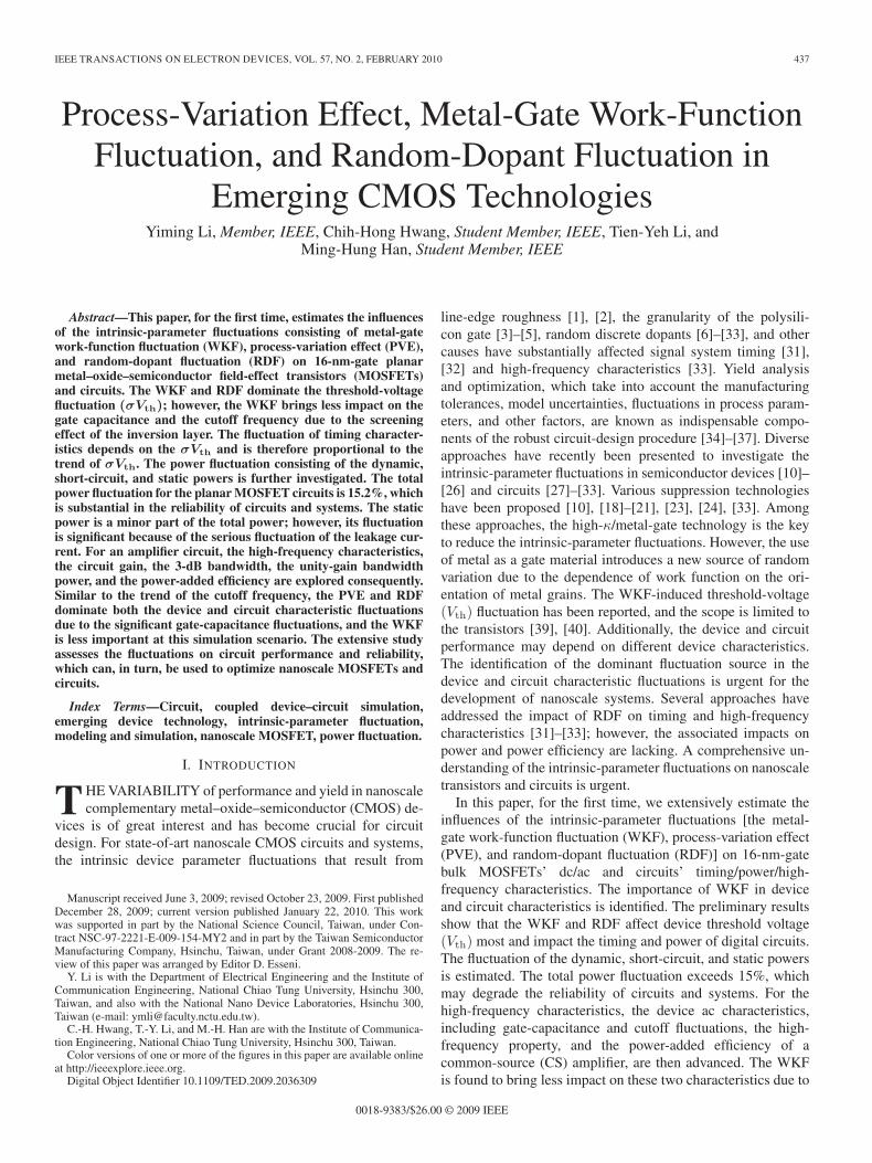
Fig. 1. (a) In a large cube of 80 × 80 × 80 nm3, 758 dopants are randomly generated, in which the equivalent doping concentration is 1.48 × 1018 cm−3. Thelarge cube is then partitioned into 125 subcubes of 16 × 16 × 16 nm3. (b)–(d) The number of dopants in a subcube may vary from 0 to 14, and the average numberis six. (e) These 125 subcubes are equivalently mapped into the device channel of bulk planar MOSFETs for the 3-D device simulation with discrete dopants.(f) Metal-gate material surface morphology, which is composed by a small number of grains. (g) PVE-induced σVth fluctuation is estimated from (h) the Vth
roll-off characteristics. (i) Tested CS amplifier and inverter circuits in this paper. (j) Simulation flowchart for the coupled device–circuit approach.
the screening effect of the inversion layer. Similar to the trendof the cutoff frequency, the PVE and RDF dominate the deviceand circuit characteristic fluctuations. The major fluctuationsources in nanoscale transistors and circuits have beenpresented herein and then verified by the related device andcircuit characteristics. The vast study assesses the fluctuationson digital-circuit performance and reliability, which maybenefit CMOS design and technology in the sub-22-nm era.
This paper is organized as follows. Section II introducesthe simulation technique for studying the effect of intrinsic-parameter fluctuations in nanoscale devices and circuits.Section III studies the characteristic fluctuations in 16-nm-gatedevices and circuits. Finally, conclusions are drawn, and thefuture work is suggested.
II. NANO-MOSFET CIRCUIT AND
SIMULATION TECHNIQUE
The devices we examined are the 16-nm-gate bulkMOSFETs (width: 16 nm) with amorphous-based TiN/HfSiONgate stacks with an EOT of 1.2 nm [39]. The RDF simulationmainly follows our recent work [20], [23], [24], [33], in which758 dopants are randomly generated in a large cube, in whichthe equivalent doping concentration is 1.48 × 1018 cm−3, asshown in Fig. 1(a). The large cube is then partitioned intosubcubes. The number of dopants may vary from 0 to 14, andthe average number is six, as shown in Fig. 1(b)–(d). Thesesubcubes are mapped into the device channel for the 3-D devicesimulation with discrete dopants, as shown in Fig. 1(e). Thedevice simulation is performed by solving a set of 3-D drift-diffusion equations with quantum corrections by the density
gradient method [42]–[49], which is conducted using a parallelcomputing system [56]–[58]. The mobility model used in thedevice simulation, according to Mathiessen’s rule [59], [60],can be expressed as
1μ
=D
μsurf_aps+
D
μsurf_rs+
1μbulk
(1)
where D = exp(x/lcrit), x is the distance from the interface,and lcrit is a fitting parameter. The mobility consists of thefollowing three parts:
1) the surface contribution due to acoustic phonon scatter-ing μsurf_aps = (B/E) + [C(Ni/N0)τ/E1/3(T/T0)K ],where Ni = NA + ND, T0 = 300 K, E is the transverseelectric field normal to the interface of the semiconductorand the insulator, B and C are parameters which arebased on physically derived quantities, N0 and τ arefitting parameters, T is lattice temperature, and K isthe temperature dependence of the probability of surfacephonon scattering;
2) the contribution attributed to surface roughness scat-tering μsurf_rs = ((E/Eref)χ/δ + E3/η)−1, where χ =A + α(n + p)Nref/(Ni + N1)ν , Eref = 1 V/cm is a ref-erence electric field to ensure a unitless numerator inμsurf_rs, Nref = 1 cm−3 is a reference doping concen-tration to cancel the unit of the term raised to the powerν in the denominator of χ, δ is a constant that dependson the details of the technology, such as oxide growthconditions, N1 = 1 cm−3, and A, α, and η are fittingparameters;

LI et al.: PVE, METAL-GATE WKF, AND RDF IN EMERGING CMOS TECHNOLOGIES 439
3) the bulk mobility μbulk = μL(T/T0)−ξ, where μL is themobility due to bulk phonon scattering and ξ is a fittingparameter.
The mobility model is quantified with our device measure-ments for the best accuracy, and the characteristic fluctuationhas been validated with the experimentally measured dc baseband data [23]. Note that, in “atomistic” device simulation, theresolution of individual charges within classical device simula-tion using a fine mesh creates problems associated with singu-larities in the Coulomb potential [15], [16], [22]. The potentialbecomes too steep with fine mesh, and therefore, the majoritycarriers are unphysically trapped by ionized impurities, andthe mobile carrier density is reduced [25], [26], [31]. Thus,the density-gradient approximation is used to handle discretecharges by properly introducing the quantum–mechanical ef-fects [42]–[49]. The physical model and accuracy of such large-scale simulation approach have been quantitatively calibratedby experimentally measured results [23].
For WKF, considering the size of metal grains and the gatearea of the devices, the device gate area is composed of a smallnumber of grains, as shown in Fig. 1(f). Each grain orientationhas a different work function; therefore, the gate work functionis a probabilistic distribution rather than a deterministic value.A statistically sound Monte Carlo approach is advanced herefor examining such distribution. At first, the gate area is par-titioned into several parts according to the average grain size,as shown in Fig. 2(a). Then, the grain orientation of each partand the total gate work function are randomly generated basedon the properties of metal, as shown in Fig. 2(b) [39], [40],[50]–[53]. The work function of each partitioned area (WKi)is a random value. The summation of WKi is then averaged toobtain the effective work function of the transistor and is thenused for WKF-induced σVth estimation. Fig. 2(c)–(e) shows theprobability distributions of work function for devices with 1, 4,9, and 16 grains on the gate area. The distribution is similarto the normal distribution as the number of grains increases.In other words, in a nanoscale transistor with scaled gate area,the distribution is not a normal distribution, and therefore, theWKF-induced σVth may not be a normal distribution as thegate area scales. Fig. 2(f) shows the dependence of the WKF-induced σVth versus the average grain size on a 16 × 16 nm2
gate area. The material is TiN. The WKF-induced σVth in-creases significantly as the average grain size increases, whichimplies the importance of controlling the metal-gate grain sizein reducing the WKF effect. The WKF-induced σVth saturatesafter the 16-nm average grain size because the average grainsize becomes larger than the gate area. The average grain sizeof this study is 4 nm [39]. Notably, the different process ofgate formulation, namely, gate first or replacement gate, maychange the thermal budget and change the grain size of themetal material. As for the PVE in Fig. 1(g), the Vth roll-offcharacteristics in Fig. 1(h) are used to estimate the effect ofPVE. The ΔLg and ΔVth are obtained from the Vth roll-offcurve. σLg is the standard deviation of the generated effectivedevice gate length. The σVth,PVE can thus be calculated fromthe equations in the inset of Fig. 1(g). The PVE includes thegate-length deviation and the line-edge roughness, whose mag-nitude follows the projections of the ITRS roadmap [54] that
Fig. 2. Gate area is partitioned into several pieces according to the averagegrain size. The work function of each partitioned area (WKi) is a randomvalue, whose probability follows (b). The obtained probability distributions ofTiN work function for devices with (c) one, (d) four, and (e) nine grains on thegate area. (f) Dependence of TiN metal-gate-induced σVth versus the averagegrain size.
3σLg= 0.7 nm and 3σLER = 0.8 nm for the 16-nm technology
node.The CS amplifier and the CMOS inverter are used as
test circuits, as shown in Fig. 1(i). Similarly, PMOSFETswith intrinsic-parameter fluctuations are generated accordingto Figs. 1 and 2. Then, the NMOSFETs and PMOSFETs arerandomly selected and used to study the circuit characteristicfluctuations. To compare fairly the NMOSFET- and PMOSFET-induced characteristic fluctuation and eliminate the effect oftransistor size on fluctuation, the dimensions of the PMOSFETwere the same as those of the NMOSFET, and the absolutevalue of the nominal threshold voltages for both the NMOSFETand PMOSFET were 140 mV. In estimating circuit character-istics, since no well-established compact model of ultrasmallnanoscale devices is available, to capture the discrete-dopant-position-induced fluctuations, a coupled device–circuit sim-ulation approach [29], [33], [41] is employed, as shown inFig. 1(j). At first, an initial guess for device bias conditionis assumed, and the device characteristics in the test circuitare estimated by solving the device transport equations. Theobtained result is the initial guess for the coupled device–circuitsimulation. Then, based on Kirchhoff’s current law, the nodalequations of the tested circuits are formulated. The formulatedcircuit equations are coupled to the device transport equationsto form a large matrix that contains both circuit and deviceequations. The large matrix is then solved for simultaneouslyobtaining device and circuit characteristics. Since the deviceequations are solved in the coupled device–circuit simulation,the effects of intrinsic-parameter fluctuations on the device and

440 IEEE TRANSACTIONS ON ELECTRON DEVICES, VOL. 57, NO. 2, FEBRUARY 2010
TABLE ISUMMARIZED Vth FLUCTUATION FOR 16-nm-GATE PLANAR NMOSFETs AND PMOSFETs, IN WHICH THE DEVICE Vth IS CALIBRATED TO 140 mV
Fig. 3. Cg–VG characteristics for the explored devices with (a) PVE, (b) WKF, and (c) RDF. (d) Cg fluctuation at VG = 0, 0.5, and 1 V for 16-nm-gateMOSFETs with WKF, PVE, and RDF.
circuit characteristics are thus properly captured. The coupledsimulation is solved iteratively until the solution is converged ineach time step and bias condition. The characteristic fluctuationof devices was validated with reference to the experimentallymeasured data [23] to ensure the best accuracy.
III. RESULTS AND DISCUSSION
In this section, the device intrinsic-parameter fluctuations forthe 16-nm-gate bulk planar MOSFETs are examined in terms ofVth, the gate capacitance (Cg), and the cutoff frequency (FT ).Then, the intrinsic-parameter fluctuation on various electricalcharacteristics including the delay, the power, and the high-frequency characteristic fluctuations are explored.
A. Device-Level Characteristics
The Vth fluctuations of NMOSFETs and PMOSFETs are ex-amined in Table I. According to the statistical independence ofthe fluctuation components, the total Vth fluctuation (σVth,total)
could be approximately given by
(σVth,total)2 ≈ (σVth,RDF)2 + (σVth,WKF)2 + (σVth,PVE)2
(2)
in which σVth,RDF, σVth,WKF, and σVth,PVE are the RDF-,WKF-, and process-variation-induced Vth fluctuation, respec-
tively. The results show that the RDF dominates the Vth fluc-tuation in NMOSFETs; however, for the Vth fluctuation ofPMOS, the WKF becomes the dominating factor because ofthe large deviation of the work function for different grainorientations in Fig. 2(b). Notably, the statistical addition ofindividual fluctuation sources herein, i.e., (2), simplifies thevariability analysis of nanodevices and circuits significantly[25]. The dominant source of fluctuation will not be signifi-cantly altered. The WKF-, PVE-, and RDF-fluctuated Cg’s areshown in Fig. 3(a)–(c), where the solid line shows the nom-inal case with 16-nm-gate 1.48 × 1018 cm−3 channel dopingand the dashed lines are the fluctuated cases. The differentintrinsic-parameter fluctuations induced rather different C–Vcharacteristics. Fig. 3(d) shows the gate-capacitance fluctua-tions (σCg) with 0-, 0.5-, and 1.0-V gate biases. Different tothe results of Vth fluctuation, the WKF brought less impact ongate-capacitance fluctuation. At low or negative gate bias, theaccumulation layer screens the impact of WKF. Additionally,at low gate bias, the total capacitance decreases because ofthe increased depletion region. The associated value of Cg
fluctuation is small. The capacitive response is then dominatedby increment of inversion in the moderate inversion. The de-vice characteristics are then impacted by intrinsic-parameter-fluctuated electrostatic potentials. If the high VG is achieved,the inversion layer is formed below the surface of the gate

LI et al.: PVE, METAL-GATE WKF, AND RDF IN EMERGING CMOS TECHNOLOGIES 441
Fig. 4. FT characteristic fluctuation induced by (a) PVE, (b) WKF, and (c) RDF. (d) Summarized FT fluctuations with for the studied planar MOSFETs.
oxide, and the total gate capacitance is mostly contributed bythe gate-oxide capacitance (Cox). Therefore, the variation ofcapacitance now again becomes the variation of the capacitanceof the gate oxide (Cox). Under strong inversion, the gatecapacitance is dominated by the inversion layer, and a smallchange resulting from the WKF in the voltage across the MOSstructure will induce a differential change in the inversion layercharge density. The WKF is therefore bringing less impact onthe gate-capacitance fluctuation because the inversion chargeresponds to the change in capacitor voltage (i.e., the WKF isnow screened by the inversion layer). Similarly, in RDF, theimpact of the individual dopant-induced electrostatic potentialvariation is screened by the inversion layer itself. However,the screening effect of the inversion layer is weakened bydiscrete dopants positioned near the channel surface. Therefore,the gate-capacitance fluctuation is still obviously fluctuated athigh gate bias. Our preliminary results show that the RDF andPVE dominate the gate-capacitance fluctuations at all gate-biasconditions, respectively. The impacts of the WKF on Cg arereduced significantly at low and high gate voltage (VG) dueto the screening effect. Notably, the PVE brings direct impacton gate length and therefore influences the gate capacitance.The PVE-induced gate-capacitance fluctuation is independentof screening effect and should be noticed when the transistoroperated in high gate bias, as shown in Fig. 3(d).
Fig. 4(a)–(c) shows the cutoff frequency (FT =vsat/2πLg =gm/2πCg) and its fluctuation versus VG, in which the solid lineshows the nominal case with 1.48 × 1018 cm−3 channel doping,
the dashed lines are fluctuated cases, and the symbol line showsthe averaged result. The gm and vsat are the transconductanceand the saturation velocity of the transistors, respectively. Theplanar MOSFETs possess higher FT ’s than those of FinFETsdue to the smaller gate capacitance [61]; WKF-induced FT
fluctuation diminished as the saturation of the carrier velocityoccurs. However, the PVE-induced FT fluctuation is still sig-nificant, owing to the direct influence of gate length (Lg) ongate capacitance. As for RDF, the carrier-impurity scatteringalters the saturation velocity, and therefore, FT fluctuation doesnot diminish in the high-field region. Note that the nominaland the averaged values of FT are similar to the results ofWKF and PVE. However, in RDF, the deviation between thenominal and the averaged FT increases as VG increases due tothe randomness of carrier-impurity scattering events and carriervelocity variations [20]. The intrinsic-parameter-induced FT
fluctuations are shown in Fig. 4(d), where the RDF and PVE arethe two major factors. The RDF and PVE play the dominatingfactor in the FT fluctuation. Notably, the impacts of RDF andWKF on FT fluctuation are suppressed at higher VG (> 0.6 V)due to the screening effect. The obtained results are similar tothe results, as shown in Fig. 3(d), in which the WKF bringinsignificant impact on Cg and FT .
B. Digital Integrated Circuits
Fig. 5(a) shows the high-to-low and low-to-high transitioncharacteristic of the output signal, and the high-to-low delay

442 IEEE TRANSACTIONS ON ELECTRON DEVICES, VOL. 57, NO. 2, FEBRUARY 2010
Fig. 5. (a) Timing of planar MOSFET inverter circuits [(symbols) input signal and (lines) output signal]. The fluctuations of (b) tHL and (c) tLH with respect toWKF, PVE, and RDF for the MOSFET inverters.
time (tHL) and low-to-high delay time (tLH) are shown inFig. 5(b) and (c), respectively. Since the tHL and tLH are depen-dent on the Vth fluctuations for the NMOSFET and PMOSFET,respectively. The fluctuations of delay time and static noisemargin depend on the Vth fluctuation which follows the trendof Vth fluctuation. Therefore, the delay-time fluctuation followsthe trend of σVth, as shown in Table I. The RDF and WKF arethe greatest effects upon timing fluctuations, and WKF intro-duces the largest tLH fluctuation due to the large work-functiondeviation within the scaled gate area. The WKF has shownits increasing importance in nanoscale transistors, particularlyfor PMOSFETs’ characteristics. Notably, we herein use thetransistors’ gate capacitance as the load capacitance (Cload) andfocused on the device intrinsic-parameter-fluctuation-inducedcircuit variability. The result of the nominal propagation delaymay be changed as we take an additional load capacitance intoconsideration.
Fig. 6 shows the power for the studied transistors. The totalpower (Ptotal) consists of the dynamic power (Pdyn), theshort-circuit power (Psc), and the static power (Pstat). Theirdefinitions are given by
Pdyn = CloadV 2ddf0−>1 (3)
Psc = f0−>1VDD
∫
T
Isc(τ)dτ (4)
Pstat = VDDIleakage. (5)
The f0−>1 is the clock rate. Isc is the short-circuit current,which is observed as both NMOSFET and PMOSFET areturned on, resulting a dc path between the power rails. T isthe switching period. Ileakage is the leakage current that flowsbetween the power rails in the absence of switching activity.The short-circuit power is determined by the time of existenceof the dc path between the power rails and the short-circuit
Fig. 6. Nominal power for the bulk planar MOSFET circuits.
current. Since the Vth for the explored devices are calibrated,the Psc is then determined by the Isc. The Isc is dependenton the saturation current of the devices. The Pdyn and Psc
are the two significant factors in total power consumption. Thecorresponding power fluctuations are further shown in Fig. 7.Fig. 7(a) shows the fluctuations of the dynamic power (σPdyn)of the bulk planar MOSFET inverter circuits with WKF, PVE,and RDF. The RDF and PVE dominate the dynamic powerfluctuation; additionally, the WKF shows less impact due to thesmaller gate-capacitance fluctuations. Fig. 7(b) shows the short-circuit-power fluctuation (σPsc) for the studied inverter cir-cuits. The short-circuit power is defined by the time of existenceof the dc path between the power rails and the short-circuitcurrent and depends on the threshold voltage of NMOSFETsand PMOSFETs, as shown in the inset of Fig. 7(b). The short-circuit-power fluctuation is therefore determined by the σVth
of the transistors. Thus, the RDF and WKF dominate the σPsc,which is similar to the result of Table I. The WKF starts to playan important role in the σPsc of planar MOSFETs because ofthe significant σVth induced by WKF. Fig. 7(c) shows the static

LI et al.: PVE, METAL-GATE WKF, AND RDF IN EMERGING CMOS TECHNOLOGIES 443
Fig. 7. (a) Dynamic power. (b) Short-circuit power. (c) Static power. (d) Total power fluctuations for the explored devices with WKF, PVE, and RDF.
power fluctuation (σPstat). Since the leakage current is an ex-ponential function of Vth(Ileakage ∝ exp(−qVth/nkT )) [55],the static power fluctuation becomes significant even though thestatic power is not an important part in total power dissipation.Moreover, the RDF dominates the σPstat due to the largerVth fluctuation. Fig. 7(d) shows the total power fluctuations(σPtotal = [(σPPVE)2 + (σPWKF)2 + (σPRDF)2]0.5), wherethe RDF dominates the total power fluctuation. The total powerfluctuation is 0.0564 μW, which is 15.2% (σPtotal/Ptotal =0.0564/0.37) of the total power. The significant power fluctu-ation may bring sizable impacts on the reliability of circuits,such as temperature, and, in turn, degrades the device perfor-mance. The remarkable components of the intrinsic-parameterfluctuations in circuit power are the RDF and WKF.
C. Analog/High-Frequency Circuits
Fig. 8 shows the characteristics of the employed CS power-amplifier circuits. The nominal output power, the circuit gain,and the power-added efficiency of the CS power amplifier as afunction of the input power are plotted, where Pout and Pin areoutput and input powers, respectively. A sinusoid input wavewith 0.5-V offset voltage is used as input signal. The devicechannel is continuously doped, and the operation frequency is108 Hz. Owing to the limitation of output signal swing, thenominal value of Pout is saturated after 10-dBm input power,which, in turn, decreases the gain of the circuit. The gainfluctuations of the planar MOSFETs resulted from WKF, PVE,and RDF are then shown in Fig. 9(a)–(d). Since the PVE andRDF dominate gate-capacitance fluctuations due to the signif-icantly affected channel length and depletion region, the PVEand RDF play important roles in high-frequency characteristicfluctuation, as shown in Fig. 9(d). The effects of WKF in
Fig. 8. Output power, circuit gain, and power-added efficiency of the exploreddevices as a function of input power. The calculation of PAE follows theformula, as shown in the inset.
high-frequency characteristics are negligible in this scenario.Additionally, the input signal is a sinusoid wave; therefore,the device may operate in a different operational region if theamplitude of the sinusoid wave is large enough. The enlargedgain fluctuation with increasing input power is resulted from thelarger portion of device operation in the linear region. Whilethe magnitude of the input signal swing increases larger than0.178 V (the input power is larger than 15 dBm), a part of deviceoperation enters the cutoff region and therefore decreases thegain fluctuation. The high-frequency characteristic fluctuationsare then shown in Fig. 10(a), where the fluctuation of the high-frequency circuit gain, the 3-dB bandwidth, and the unity-gain bandwidth are extracted, as shown in Fig. 10(b)–(d),respectively. Similar to the result of Figs. 2 and 3, the RDF andPVE dominate the high-frequency characteristic fluctuations,and WKF becomes marginal in this analyzing skeleton.

444 IEEE TRANSACTIONS ON ELECTRON DEVICES, VOL. 57, NO. 2, FEBRUARY 2010
Fig. 9. Circuit gain characteristics of the planar MOSFETs with (a) PVE, (b) WKF, and (c) RDF fluctuations, respectively. (d) Summarized circuit gainfluctuations.
Fig. 10. (a) Frequency response of the planar MOSFET CS amplifiers, in which (b) 3-dB bandwidth, (c) gain, and (d) unity-gain bandwidth fluctuations areextracted.
IV. CONCLUSION
In this paper, we have estimated the influences of theintrinsic-parameter fluctuations in 16-nm planar MOSFETs andcircuits. Our preliminary results have shown that the WKF
and RDF dominate the device threshold-voltage fluctuation andtherefore rule the delay time of the explored digital invertercircuits. The fluctuation of delay time depends on the Vth
fluctuation which follows the trend of Vth fluctuation. The

LI et al.: PVE, METAL-GATE WKF, AND RDF IN EMERGING CMOS TECHNOLOGIES 445
WKF effect in PMOSFETs may bring significant impact ontLH characteristics due to the large difference of work func-tion in different grain orientations. The total power fluctua-tion including the fluctuations of the dynamic, short-circuit,and static powers is about 15.2% for the planar MOSFETs,which may induce significant performance uncertainties, suchas temperature and timing, to degrade the reliability of circuitsand systems. The dynamic and short-circuit powers are themost important power-dissipation sources. However, the static-power fluctuation dominates the total power fluctuation due tothe exponential relationship between the leakage current andthe Vth. The significant leakage-power fluctuation was furtherinvestigated, which should be considered in robust circuit andsystem design. For the high-frequency characteristics, the cir-cuit gain, the power, and the power-added efficiency were alsoexplored. Similar to the trend of the device cutoff frequency,the PVE and RDF dominate the device and circuit characteristicfluctuations, and the WKF shows less impact on high-frequencycharacteristics, owing to the small gate-capacitance fluctuation.The sensitivities of circuit performance with respect to deviceparameter fluctuation have been reported. It is necessary toinclude both the WKF and RDF effects in studying digital-circuit reliability; however, for the high-frequency applications,the PVE and RDF effects are dominating factors. We arecurrently working on the study of the possible correlationsbetween each fluctuation source. The interaction of Vth changedue to different sources may be important and need to be prop-erly incorporated. Additionally, the 3-D Monte Carlo devicesimulation with, for example, ab initio impurity scattering [17],[26], may provide more rich physical insights and accurateestimations, which will also be addressed in our future work.
REFERENCES
[1] A. Asenov, S. Kaya, and A. R. Brown, “Intrinsic parameter fluctua-tions in decananometer MOSFETs introduced by gate line edge rough-ness,” IEEE Trans. Electron Devices, vol. 50, no. 5, pp. 1254–1260,May 2003.
[2] G. Roy, A. R. Brown, F. Adamu-Lema, S. Roy, and A. Asenov, “Sim-ulation study of individual and combined sources of intrinsic param-eter fluctuations in conventional nano-MOSFETs,” IEEE Trans. ElectronDevices, vol. 53, no. 12, pp. 3063–3070, Dec. 2006.
[3] H. P. Tuinhout, A. H. Montree, J. Schmitz, and P. A. Stolk, “Effects of gatedepletion and boron penetration on matching of deep submicron CMOStransistor,” in IEDM Tech. Dig., 1997, pp. 631–634.
[4] A. R. Brown, G. Roy, and A. Asenov, “Poly-Si-gate-related variability indecananometre MOSFETs with conventional architecture,” IEEE Trans.Electron Devices, vol. 54, no. 11, pp. 3056–3063, Nov. 2007.
[5] R. W. Keyes, “Effect of randomness in distribution of impurity atoms onFET thresholds,” Appl. Phys., vol. 8, no. 3, pp. 251–259, Nov. 1975.
[6] R. P. Joshi and D. K. Ferry, “Effect of multi-ion screening on the elec-tronic transport in doped semiconductors: A molecular-dynamics analy-sis,” Phys. Rev. B, Condens. Matter, vol. 43, no. 12, pp. 9734–9739,Apr. 1991.
[7] P. Francis, A. Terao, and D. Flandre, “Modeling of ultrathin double-gateNMOS/SOI transistors,” IEEE Trans. Electron Devices, vol. 41, no. 5,pp. 715–720, May 1994.
[8] J.-R. Zhou and D. K. Ferry, “3D simulation of deep-submicron devices:How impurity atoms affect conductance,” IEEE Comput. Sci. Eng., vol. 2,no. 2, pp. 30–37, Jun. 1995.
[9] X.-H. Tang, V. K. De, and J. D. Meindl, “Intrinsic MOSFET parameterfluctuations due to random dopant placement,” IEEE Trans. Very LargeScale Integr. (VLSI) Syst., vol. 5, no. 4, pp. 369–376, Dec. 1997.
[10] K. Noda, T. Tatsumi, T. Uchida, K. Nakajima, H. Miyamoto, and C. Hu,“A 0.1- μm delta doped MOSFET fabricated with post-low-energy im-planting selective epitaxy,” IEEE Trans. Electron Devices, vol. 45, no. 4,pp. 809–813, Apr. 1998.
[11] P. A. Stolk, F. P. Widdershoven, and D. B. M. Klaassen, “Modelingstatistical dopant fluctuations in MOS transistors,” IEEE Trans. ElectronDevices, vol. 45, no. 9, pp. 1960–1971, Sep. 1998.
[12] D. Vasileska, W. J. Gross, and D. K. Ferry, “Modeling of deep-submicrometer MOSFETs: Random impurity effects, threshold voltageshifts and gate capacitance attenuation,” in Proc. Ext. Abstr. Int. WorkshopComput. Electron., Oct. 1998, pp. 259–262.
[13] W. J. Gross, D. Vasileska, and D. K. Ferry, “A novel approach forintroducing the electron–electron and electron-impurity interactions inparticle-based simulations,” IEEE Electron Device Lett., vol. 20, no. 9,pp. 463–465, Sep. 1999.
[14] H.-S. Wong, Y. Taur, and D. J. Frank, “Discrete random dopant dis-tribution effects in nanometer-scale MOSFETs,” Microelectron. Reliab.,vol. 38, no. 9, pp. 1447–1456, Sep. 1999.
[15] N. Sano, K. Matsuzawa, M. Mukai, and N. Nakayama, “Role of long-range and short-range Coulomb potentials in threshold characteristicsunder discrete dopants in sub-0.1 μm Si-MOSFETs,” in IEDM Tech. Dig.,Dec. 2000, pp. 275–278.
[16] N. Sano, K. Matsuzawa, M. Mukai, and N. Nakayama, “On dis-crete random dopant modeling in drift-diffusion simulations: Physicalmeaning of ‘atomistic’ dopants,” Microelectron. Reliab., vol. 42, no. 2,pp. 189–199, Feb. 2002.
[17] P. Dollfus, A. Bournel, S. Galdin, S. Barraud, and P. Hesto, “Effect ofdiscrete impurities on electron transport in ultrashort MOSFET using 3DMC simulation,” IEEE Trans. Electron Devices, vol. 51, no. 5, pp. 749–756, May 2004.
[18] Y. Li and S.-M. Yu, “Comparison of random-dopant-induced thresholdvoltage fluctuation in nanoscale single-, double-, and surrounding-gatefield-effect transistors,” Jpn. J. Appl. Phys., vol. 45, no. 9A, pp. 6860–6865, Sep. 2006.
[19] T. Ohtou, N. Sugii, and T. Hiramoto, “Impact of parameter variationsand random dopant fluctuations on short-channel fully depleted SOIMOSFETs with extremely thin BOX,” IEEE Electron Device Lett.,vol. 28, no. 8, pp. 740–742, Aug. 2007.
[20] Y. Li and C.-H. Hwang, “Discrete-dopant-induced characteristic fluctua-tions in 16 nm multiple-gate silicon-on-insulator devices,” J. Appl. Phy.,vol. 102, no. 8, p. 084509, Oct. 2007.
[21] Y. Li and S.-M. Yu, “A coupled-simulation-and-optimization approachto nanodevice fabrication with minimization of electrical characteristicsfluctuation,” IEEE Trans. Semicond. Manuf., vol. 20, no. 4, pp. 432–438,Nov. 2007.
[22] N. Sano and M. Tomizawa, “Random dopant model for three-dimensionaldrift-diffusion simulations in metal-oxide-semiconductor field-effect-transistors,” Appl. Phy. Lett., vol. 79, no. 14, p. 2267, 2007.
[23] Y. Li, S.-M. Yu, J.-R. Hwang, and F.-L. Yang, “Discrete dopant fluctuated20 nm/15 nm-gate planar CMOS,” IEEE Trans. Electron Devices, vol. 55,no. 6, pp. 1449–1455, Jun. 2008.
[24] Y. Li, C.-H. Hwang, and H.-M. Huang, “Large-scale ‘atomistic’ ap-proach to discrete-dopant-induced characteristic fluctuations in siliconnanowire transistors,” Phys. Stat. Sol. (A), vol. 205, no. 6, pp. 1505–1510,May 2008.
[25] A. Asenov, A. Cathignol, B. Cheng, K. P. McKenna, A. R. Brown,A. L. Shluger, D. Chanemougame, K. Rochereau, and G. Ghibaudo,“Origin of the asymmetry in the magnitude of the statistical variabilityof n- and p-channel poly-Si gate bulk MOSFETs,” IEEE Electron DeviceLett., vol. 29, no. 8, pp. 913–915, Aug. 2008.
[26] C. L. Alexander, G. Roy, and A. Asenov, “Random impurity scatteringinduced variability in conventional nano-scaled MOSFETs: Ab initioimpurity scattering Monte Carlo simulation study,” in IEDM Tech. Dig.,Nov. 2006, pp. 949–952.
[27] A. Balasubramanian, P. R. Fleming, B. L. Bhuva, A. L. Sternberg, andL. W. Massengill, “Implications of dopant-fluctuation-induced Vt varia-tions on the radiation hardness of deep submicrometer CMOS SRAMs,”IEEE Trans. Device Mater. Rel., vol. 8, no. 1, pp. 135–144, Mar. 2003.
[28] S. K. Springer, S. Lee, N. Lu, E. J. Nowak, J.-O. Plouchart, J. S. Watts,R. Q. Williams, and N. Zamdmer, “Modeling of variation insubmicrometer CMOS ULSI technologies,” IEEE Trans. Electron De-vices, vol. 53, no. 9, pp. 2168–2178, Sep. 2006.
[29] R. Tanabe, Y. Ashizawa, and H. Oka, “Investigation of SNM with randomdopant fluctuations for FD SGSOI and FinFET 6T SOI SRAM cell bythree-dimensional device simulation,” in Proc. Simul. Semicond. Process.Device Conf., Sep. 2006, pp. 103–106.
[30] B. Cheng, S. Roy, G. Roy, and A. Asenov, “Impact of intrinsic parameterfluctuations on SRAM cell design,” in Proc. Int. Solid-State Integr. CircuitTechnol. Conf., Oct. 2006, pp. 1290–1292.
[31] X. Tang, K. A. Bowman, J. C. Eble, V. K. De, and J. D. Meindl,“Impact of random dopant placement on CMOS delay and power

446 IEEE TRANSACTIONS ON ELECTRON DEVICES, VOL. 57, NO. 2, FEBRUARY 2010
dissipation,” in Proc. 29th Eur. Solid-State Device Res. Conf., Sep. 1999,pp. 184–187.
[32] H. Mahmoodi, S. Mukhopadhyay, and K. Roy, “Estimation of delayvariations due to random-dopant fluctuations in nanoscale CMOS cir-cuits,” IEEE J. Solid-State Circuits, vol. 40, no. 9, pp. 1787–1796,Sep. 2005.
[33] Y. Li and C.-H. Hwang, “High-frequency characteristic fluctuations ofnano-MOSFET circuit induced by random dopants,” IEEE Trans. Microw.Theory Tech., vol. 56, no. 12, pp. 2726–2733, Dec. 2008.
[34] A. Hafid Zaabab, Q.-J. Zhang, and M. Nakhla, “A neural network model-ing approach to circuit optimization and statistical design,” IEEE Trans.Microw. Theory Tech., vol. 43, no. 6, pp. 1349–1358, Jun. 1995.
[35] P. Crippa, C. Turchetti, and M. Conti, “A statistical methodology forthe design of high-performance CMOS current-steering digital-to-analogconverters,” IEEE Trans. Comput.-Aided Design Integr. Circuits Syst.,vol. 21, no. 4, pp. 377–394, Apr. 2002.
[36] J. Jaffari and M. Anis, “Variability-aware bulk-MOS device design,”IEEE Trans. Comput.-Aided Design Integr. Circuits Syst., vol. 27, no. 2,pp. 205–216, Feb. 2008.
[37] L. Brusamarello, R. da Silva, G. I. Wirth, and R. A. L. Reis, “Probabilis-tic approach for yield analysis of dynamic logic circuits,” IEEE Trans.Circuits Syst. I, Reg. Papers, vol. 55, no. 8, pp. 2238–2248, Sep. 2008.
[38] H. Nho, S.-S. Yoon, S. S. Wong, and S.-O. Jung, “Numerical estimation ofyield in sub-100-nm SRAM design using Monte Carlo simulation,” IEEETrans. Circuits Syst. I, Exp. Briefs, vol. 55, no. 9, pp. 907–911, Sep. 2008.
[39] K. Ohmori, T. Matsuki, D. Ishikawa, T. Morooka, T. Aminaka, Y. Sugita,T. Chikyow, K. Shiraishi, Y. Nara, and K. Yamada, “Impact of additionalfactors in threshold voltage variability of metal/high-k gate stacks and itsreduction by controlling crystalline structure and grain size in the metalgates,” in IEDM Tech. Dig., Dec. 2008, pp. 1–4.
[40] H. Dadgour, V. De, and K. Banerjee, “Statistical modeling of metal-gatework-function variability in emerging device technologies and implica-tions for circuit design,” in Proc. ICCAD, 2008, pp. 270–277.
[41] T. Grasser and S. Selberherr, “Mixed-mode device simulation,” Micro-electron. J., vol. 31, no. 11/12, pp. 873–881, Dec. 2000.
[42] G. J. Iafrate, H. L. Grubin, and D. K. Ferry, “Utilization of quantumdistribution functions for ultra-submicron device transport,” Le Journalde Physique Colloques, vol. 42, no. C7, p. C7-307, 1981.
[43] M. G. Ancona and H. F. Tiersten, “Macroscopic physics of the siliconinversion layer,” Phys. Rev. B, Condens. Matter, vol. 35, no. 15, pp. 7959–7965, May 1987.
[44] J.-R. Zhou and D. K. Ferry, “Simulation of ultra-small GaAs MESFET us-ing quantum moment equations,” IEEE Trans. Electron Devices, vol. 39,no. 3, pp. 473–478, Mar. 1992.
[45] J.-R. Zhou and D. K. Ferry, “Simulation of ultra-small GaAs MESFETsusing quantum moment equations. II. Velocity overshoot,” IEEE Trans.Electron Devices, vol. 39, no. 8, pp. 1793–1796, Aug. 1992.
[46] J.-R. Zhou and D. K. Ferry, “Modeling of quantum effects in ultrasmallHEMT devices,” IEEE Trans. Electron Devices, vol. 40, no. 2, pp. 421–427, Feb. 1993.
[47] T.-W. Tang, X. Wang, and Y. Li, “Discretization scheme for the density-gradient equation and effect of boundary conditions,” J. Comput. Elec-tron., vol. 1, no. 3, pp. 389–393, Oct. 2002.
[48] G. Roy, A. R. Brown, A. Asenov, and S. Roy, “Quantum aspects ofresolving discrete charges in ‘atomistic’ device simulations,” J. Comput.Electron., vol. 2, no. 2–4, pp. 323–327, Dec. 2003.
[49] S. Odanaka, “Multidimensional discretization of the stationary quantumdrift-diffusion model for ultrasmall MOSFET structures,” IEEE Trans.Comput.-Aided Design Integr. Circuit Syst., vol. 23, no. 6, pp. 837–842,Jun. 2004.
[50] S. Berge, P.O. Gartland, and B.J. Slagsvold, “Photoelectric work functionof a molybdenum single crystal for the (100), (110), (111), (112), (114),and (332) faces,” Surf. Sci., vol. 43, no. 1, pp. 275–292, May 1974.
[51] A. Yagishita, T. Saito, K. Nakajima, S. Inumiya, K. Matsuo, T. Shibata,Y. Tsunashima, K. Suguro, and T. Arikado, “Improvement of thresh-old voltage deviation in damascene metal gate transistors,” IEEE Trans.Electron Devices, vol. 48, no. 8, pp. 1604–1611, Aug. 2001.
[52] J. L. He, Y. Setsuhara, I. Shimizu, and S. Miyake, “Structure refine-ment and hardness enhancement of titanium nitride films by addition ofcopper,” Surf. Coat. Technol., vol. 137, no. 1, pp. 38–42, Mar. 2001.
[53] H. Daewon, H. Takeuchi, Y.-K. Choi, and T.-J. King, “Molybdenum gatetechnology for ultrathin-body MOSFETs and FinFETs,” IEEE Trans.Electron Devices, vol. 51, no. 12, pp. 1989–1996, Dec. 2004.
[54] [Online]. Available: http://www.itrs.net[55] G. Jie, S. S. Sapatnekar, and C. Kim, “Width-dependent statistical leakage
modeling for random dopant induced threshold voltage shift,” in Proc. Int.Conf. DAC, 2007, pp. 87–92.
[56] Y. Li and S.-M. Yu, “A parallel adaptive finite volume method fornanoscale double-gate MOSFETs simulation,” J. Comput. Appl. Math.,vol. 175, no. 1, pp. 87–99, Mar. 2005.
[57] Y. Li, H.-M. Lu, T.-W. Tang, and S. M. Sze, “A novel parallel adaptiveMonte Carlo method for nonlinear Poisson equation in semiconductordevices,” Math. Comput. Simul., vol. 62, no. 3–6, pp. 413–420, Mar. 2003.
[58] Y. Li, S. M. Sze, and T. S. Chao, “A practical implementation of paralleldynamic load balancing for adaptive computing in VLSI device simula-tion,” Eng. Comput., vol. 18, no. 2, pp. 124–137, Aug. 2002.
[59] M. N. Darwish, J. L. Lentz, M. R. Pinto, P. M. Zeitzoff, and T. JuongKrutsick, “An improved electron and hole mobility model for generalpurpose device simulation,” IEEE Trans. Electron Devices, vol. 44, no. 9,pp. 1529–1538, Sep. 1997.
[60] S. Selberherr, Analysis and Simulation of Semiconductor Devices.New York: Springer-Verlag, 1984.
[61] P. Wambacq, B. Verbruggen, K. Scheir, J. Borremans, M. Dehan,D. Linten, V. D. Heyn, G. V. Plas, A. Mercha, B. Parvais, C. Gustin,V. Subramanian, N. Collaert, M. Jurczak, and S. Decoutere, “The potentialof FinFETs for analog and RF circuit applications,” IEEE Trans. CircuitsSyst. I, Reg. Papers, vol. 54, no. 11, pp. 2541–2551, Nov. 2007.
Yiming Li (M’02) received the B.S. degree in ap-plied mathematics and electronics engineering, theM.S. degree in applied mathematics, and the Ph.D.degree in electronics from the National Chiao TungUniversity (NCTU), Hsinchu, Taiwan, in 1996, 1998,and 2001, respectively.
In 2001, he joined the National Nano DeviceLaboratories (NDL), Hsinchu, as an Associate Re-searcher, and the Microelectronics and InformationSystems Research Center (MISRC), NCTU, as anAssistant Professor, where he has been engaged in
the field of computational science and engineering, particularly in modeling,simulation, and optimization of nanoelectronics and very large scale integration(VLSI) circuits. In the fall of 2002, he was a Visiting Assistant Professorwith the Department of Electrical and Computer Engineering, University ofMassachusetts, Amherst. From 2003 to 2004, he was a Research Consultantwith the System on a Chip (SoC) Technology Center, Industrial TechnologyResearch Institute, Hsinchu. From 2003 to 2005, he was the Director of theDepartments of Nanodevice and Computational Nanoelectronics, NDL, andsince the fall of 2004, he was an Associate Professor with MISRC. From thefall of 2005 to fall of 2008, he was an Associate Professor with the Departmentof Communication Engineering, NCTU, where he is currently a Full Professorwith the Department of Electrical Engineering, is the Deputy Director of theModeling and Simulation Center, and conducts the Parallel and ScientificComputing Laboratory. He is also the Deputy Director General of NDL. Hiscurrent research areas include computational electronics and physics, physicsof semiconductor nanostructures, device modeling, parameter extraction, VLSIcircuit simulation, development of technology computer-aided-design (CAD)and electronic CAD tools and SoC applications, bioinformatics and computa-tional biology, advanced numerical methods, parallel and scientific computing,optimization techniques, and computational intelligence. He has authored orcoauthored over 120 research papers appearing in international book chapters,journals, and conferences. He has served as a Reviewer, Guest Associate Editor,Guest Editor, Associate Editor, and Editor for many international journals.
Dr. Li is a member of Phi Tau Phi, Sigma Xi, the American Physical Society,the American Chemical Society, the Association for Computing Machinery, theInstitute of Electronics, Information and Communication Engineers, Japan, andthe Society for Industrial and Applied Mathematics. He is included in Who’sWho in the World. He was the recipient of the 2002 Research Fellowship Awardpresented by the Pan Wen-Yuan Foundation, Taiwan, and the 2006 OutstandingYoung Electrical Engineer Award from the Chinese Institute of Electrical En-gineering, Taiwan. He has served as a Reviewer for the IEEE TRANSACTIONS
ON EVOLUTIONARY COMPUTATION, the IEEE TRANSACTIONS ON NANO-TECHNOLOGY, the IEEE TRANSACTIONS ON MICROWAVE THEORY AND
TECHNIQUES, the IEEE TRANSACTIONS ON COMPUTER-AIDED DESIGN
OF INTEGRATED CIRCUITS AND SYSTEMS, the IEEE ELECTRON DEVICE
LETTERS, and the IEEE TRANSACTIONS ON ELECTRON DEVICES. He hasorganized and served on several international conferences and was an Editorfor proceedings of international conferences.

LI et al.: PVE, METAL-GATE WKF, AND RDF IN EMERGING CMOS TECHNOLOGIES 447
Chih-Hong Hwang (S’08) received the B.S. de-gree in engineering and system science and theM.S. degree in electronics engineering from NationalTsing Hua University, Hsinchu, Taiwan, in 2001 and2003, respectively. He is currently working towardthe Ph.D. degree in the Parallel and Scientific Com-puting Laboratory, Institute of Communication Engi-neering, National Chiao Tung University, Hsinchu.
His research interests focus on modeling and sim-ulation of semiconductor nanodevices and variabilityof nano-CMOS devices and circuits.
Mr. Hwang was the recipient of the Bronze Medal of the 2008 TSMCOutstanding Student Research Award presented by Taiwan SemiconductorManufacturing Company, Hsinchu, and the 2008 EDA Top-Notch InternationalConference Paper Award from Electronic Design Automation Consortium,Taiwan.
Tien-Yeh Li received the B.S. degree in electricalengineering from National Taiwan Ocean University,Keelung, Taiwan, in 2006. He is currently workingtoward the M.S. degree in the Parallel and Scien-tific Computing Laboratory, Institute of Communi-cation Engineering, National Chiao Tung University,Hsinchu, Taiwan.
His research interests focus on modeling and sim-ulation of semiconductor nanodevices, particularlynanomemory devices.
Mr. Li was the recipient of the 2008 EDA Top-Notch International Conference Paper Award from the Electronic DesignAutomation Consortium, Taiwan.
Ming-Hung Han (S’09) received the B.S. degreein communication engineering from National ChiaoTung University, Hsinchu, Taiwan in 2006, wherehe is currently working toward the M.S. degree inthe Parallel and Scientific Computing Laboratory,Institute of Communication Engineering.
His research interests focus on modeling andsimulation of high-frequency semiconductornanodevices.