product brochure mp1595a - dl.cdn-anritsu.com · product brochure mp1595a ... this all-in-one...
TRANSCRIPT
Product Brochure
MP1595A40G SDH/SONET Analyzer
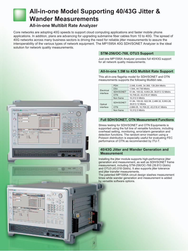
All-in-one Model Supporting 40/43G Jitter & Wander MeasurementsAll-in-one Multibit Rate Analyzer
Core networks are adopting 40G speeds to support cloud computing applications and faster mobile phone applications. In addition, plans are advancing for upgrading submarine fiber cables from 10 to 40G. The spread of 40G networks across many business sectors is driving the need for reliable jitter measurements to assure the interoperability of the various types of network equipment. The MP1595A 40G SDH/SONET Analyzer is the ideal solution for network quality measurements.
STM-256/OC-768, OTU3 SupportJust one MP1595A Analyzer provides full 40/43G support for all network quality measurements.
All-In-one 1.5M to 43G Multibit Rate SupportThis all-in-one flagship model for SDH/SONET and OTN measurements supports the following Multibit rate.
Electrical interface
PDH 2.048, 8.448, 34.368, 139.264 Mbit/sDSn 1.544, 44.736 Mbit/sSDH/SONET 51.84, 155.52, 9,953.28, 39,813.12 Mbit/sOTN 10,709.22, 43,018.41 Mbit/sNon frame 10,312.5 Mbit/s
Optical interface
SDH/SONET 51.84, 155.52, 622.08, 2,488.32, 9,953.28, 39,813.12 Mbit/s
OTN 2,666.05, 10,709.22, 43,018.41 Mbit/sNon frame 10,312.5 Mbit/s
Full SDH/SONET, OTN Measurement FunctionsStress testing for SDH/SONET and OTN Equipments is supported using the full line of versatile functions, including overhead setting, monitoring, error/alarm generation and detection functions. The random error insertion using a Poisson distribution is especially useful for evaluating FEC performance of OTN as recommended by ITU-T.
40/43G Jitter and Wander Generation and Measurement
Installing the jitter module supports high-performance jitter generation and measurement, as well as SDH/SONET frame measurement, including STM-256/OC-768 (39.813 Gbit/s) and OTU3 (43.018 Gbit/s). It also supports jitter tolerance and jitter transfer measurements.The patented MP1595A circuit design slashes measurement times while wander generation and measurement is added by versatile software options.
2
3
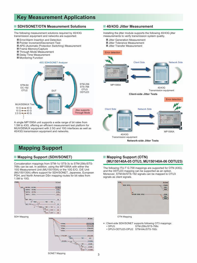
SDH/SONET/OTN Measurement SolutionsThe following measurement solutions required by 40/43G transmission equipment and networks are supported:
Error/Alarm Insertion and Detection Pointer Increment/Decrement Test APS (Automatic Protection Switching) Measurement Frame Memory/Capture Through Mode Measurement Delay Time Measurement Monitoring Function
A single MP1595A unit supports a wide range of bit rates from 1.5M to 43G, offering an efficient measurement test platform for MUX/DEMUX equipment with 2.5G and 10G interfaces as well as 40/43G transmission equipment and networks.
40/43G Jitter MeasurementInstalling the jitter module supports the following 40/43G jitter measurements to verify transmission system quality.
Jitter Generation Measurement Jitter Tolerance Measurement Jitter Transfer Measurement
Mapping Suppo rt (SDH/SONET)Concatenation mappings from STM-1c/ STS-3c to STM-256c/STS-768c can be set. In addition, using the MP1595A with either the 10G Measurement Unit (MU150100A) or the 10G E/O, O/E Unit (MU150135A) offers support for SDH/SONET, Japanese, European PDH, and North American DSn mapping routes for bit rates from 1.5M to 10G.
SDH Mapping
SONET Mapping
Mapping Support (OTN) (MU150140A-05 OTU3, MU150140A-06 ODTU23)
The following ITU-T G.709 mappings are supported for OTN (43G). and the ODTU23 mapping can be supported as an option. Moreover, STM-64/STS-192 signals can be mapped to OTU3 signals as client signals.
OTN Mapping
∗: Client-side SDH/SONET supports following OT3 mappings: • OPU3: STM-256c/STS-768c • OPU3-ODTU23-OPU2: STM-64c/STS-192c
Key Measurement Applications
Mapping Support
40G SDH/SONET Analyzer
DUT
STM-256 STS-768
OTU3 ODTU23
MUX/DEMUX Test10 G 40 G 10 G 43 G 2.5 G 40 G
STM-64 OC-192 OTU2
: :
Also supports Through Mode
Error detection
Network SideClient Side
40/43GTransmission equipment
MP1595A
Client-side Jitter Tests
Error detection
Network SideClient Side
40/43GTransmission equipment
MP1595A
Network-side Jitter Tests
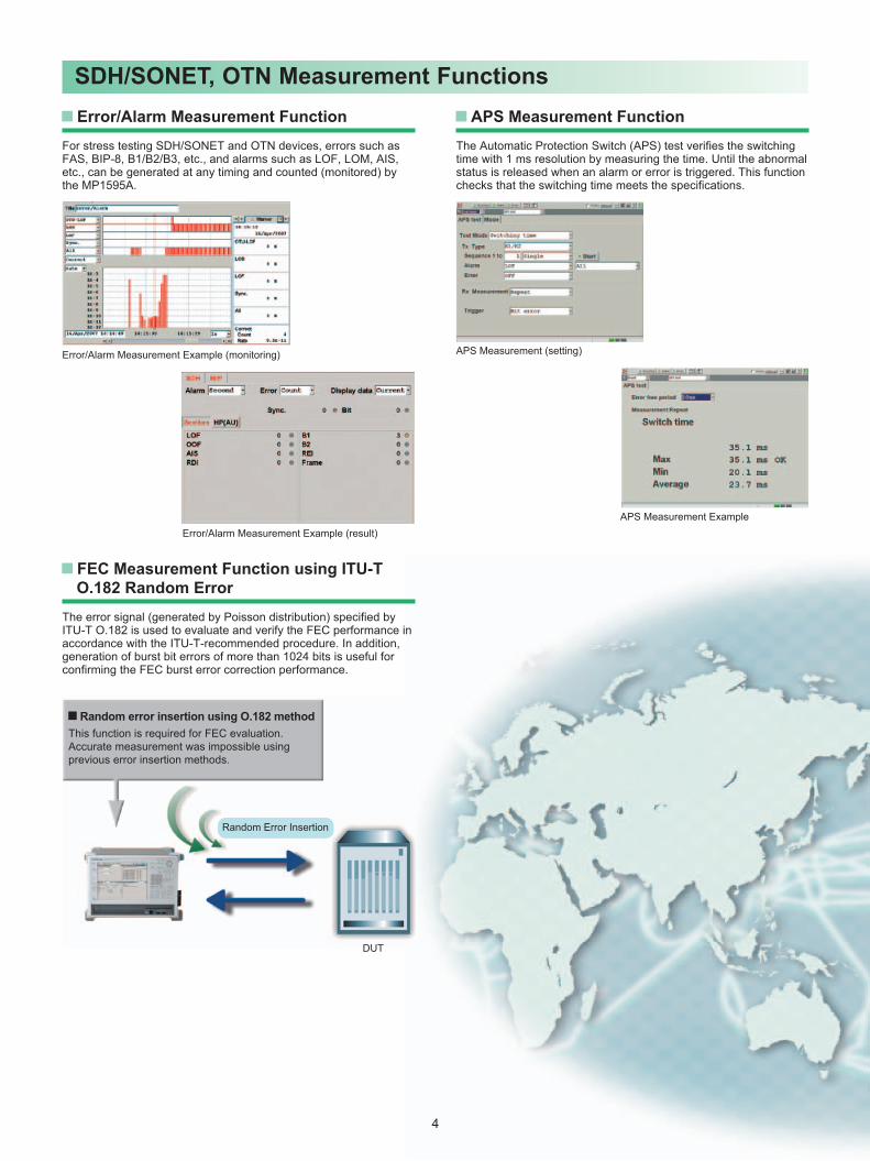
Error/Alarm Measurement FunctionFor stress testing SDH/SONET and OTN devices, errors such as FAS, BIP-8, B1/B2/B3, etc., and alarms such as LOF, LOM, AIS, etc., can be generated at any timing and counted (monitored) by the MP1595A.
APS Measurement FunctionThe Automatic Protection Switch (APS) test verifies the switching time with 1 ms resolution by measuring the time. Until the abnormal status is released when an alarm or error is triggered. This function checks that the switching time meets the specifications.
FEC Measurement Function using ITU-T O.182 Random Error
The error signal (generated by Poisson distribution) specified by ITU-T O.182 is used to evaluate and verify the FEC performance in accordance with the ITU-T-recommended procedure. In addition, generation of burst bit errors of more than 1024 bits is useful for confirming the FEC burst error correction performance.
Error/Alarm Measurement Example (monitoring) APS Measurement (setting)
APS Measurement ExampleError/Alarm Measurement Example (result)
DUT
Random error insertion using O.182 methodThis function is required for FEC evaluation. Accurate measurement was impossible using previous error insertion methods.
Random Error Insertion
SDH/SONET, OTN Measurement Functions
4
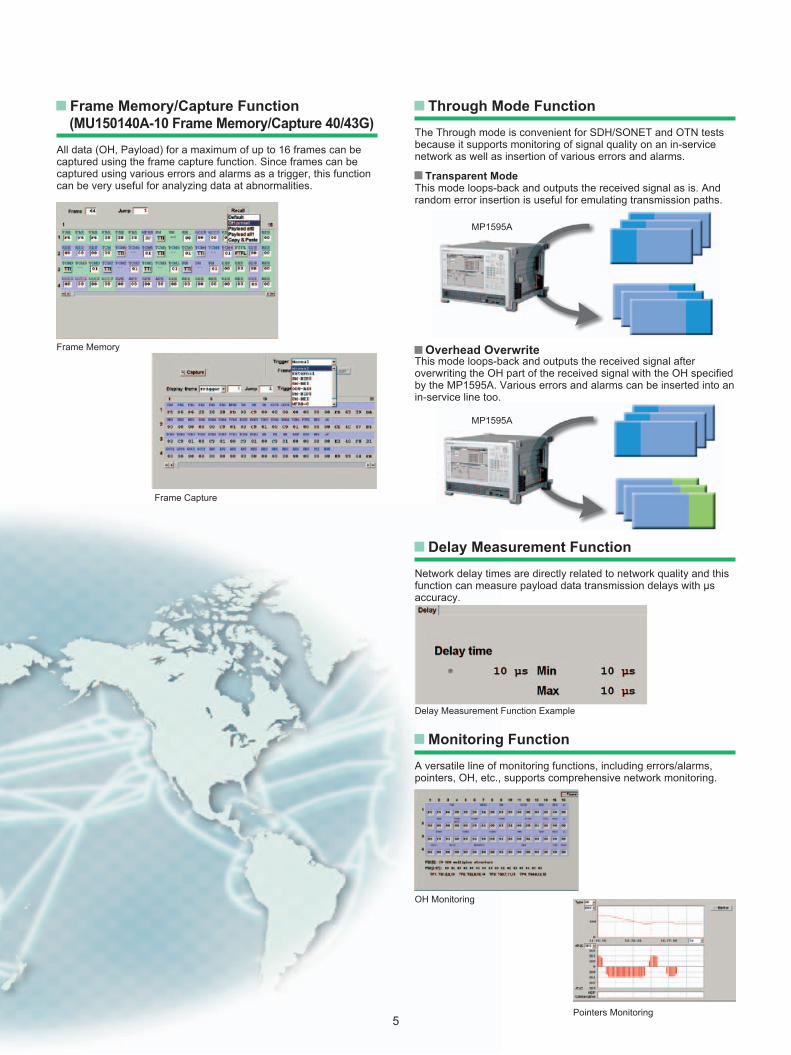
Through Mode FunctionThe Through mode is convenient for SDH/SONET and OTN tests because it supports monitoring of signal quality on an in-service network as well as insertion of various errors and alarms.
Frame Memory/Capture Function (MU150140A-10 Frame Memory/Capture 40/43G)
All data (OH, Payload) for a maximum of up to 16 frames can be captured using the frame capture function. Since frames can be captured using various errors and alarms as a trigger, this function can be very useful for analyzing data at abnormalities.
Delay Measurement FunctionNetwork delay times are directly related to network quality and this function can measure payload data transmission delays with µs accuracy.
Transparent ModeThis mode loops-back and outputs the received signal as is. And random error insertion is useful for emulating transmission paths.
Overhead OverwriteThis mode loops-back and outputs the received signal after overwriting the OH part of the received signal with the OH specified by the MP1595A. Various errors and alarms can be inserted into an in-service line too.
Monitoring FunctionA versatile line of monitoring functions, including errors/alarms, pointers, OH, etc., supports comprehensive network monitoring.
Frame Memory
MP1595A
MP1595A
Frame Capture
Delay Measurement Function Example
OH Monitoring
Pointers Monitoring5
6
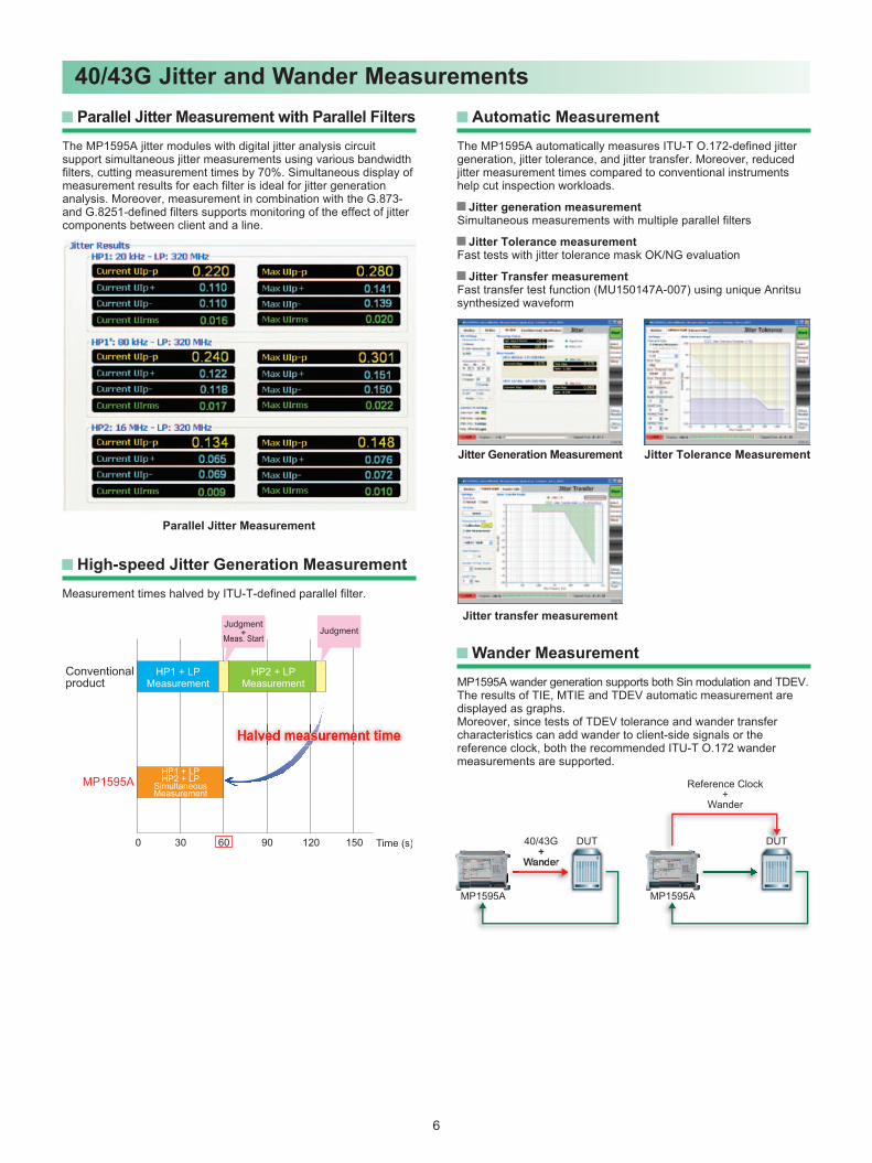
Parallel Jitter Measurement with Parallel FiltersThe MP1595A jitter modules with digital jitter analysis circuit support simultaneous jitter measurements using various bandwidth filters, cutting measurement times by 70%. Simultaneous display of measurement results for each filter is ideal for jitter generation analysis. Moreover, measurement in combination with the G.873- and G.8251-defined filters supports monitoring of the effect of jitter components between client and a line.
High-speed Jitter Generation MeasurementMeasurement times halved by ITU-T-defined parallel filter.
Wander MeasurementMP1595A wander generation supports both Sin modulation and TDEV.The results of TIE, MTIE and TDEV automatic measurement are displayed as graphs.Moreover, since tests of TDEV tolerance and wander transfer characteristics can add wander to client-side signals or the reference clock, both the recommended ITU-T O.172 wander measurements are supported.
40/43G Jitter and Wander Measurements Automatic Measurement
The MP1595A automatically measures ITU-T O.172-defined jitter generation, jitter tolerance, and jitter transfer. Moreover, reduced jitter measurement times compared to conventional instruments help cut inspection workloads.
Jitter generation measurementSimultaneous measurements with multiple parallel filters
Jitter Tolerance measurementFast tests with jitter tolerance mask OK/NG evaluation
Jitter Transfer measurementFast transfer test function (MU150147A-007) using unique Anritsu synthesized waveform
Parallel Jitter Measurement
Jitter Generation Measurement
Jitter transfer measurement
Jitter Tolerance Measurement
7
Optical Level Monitoring
Frequency Monitoring
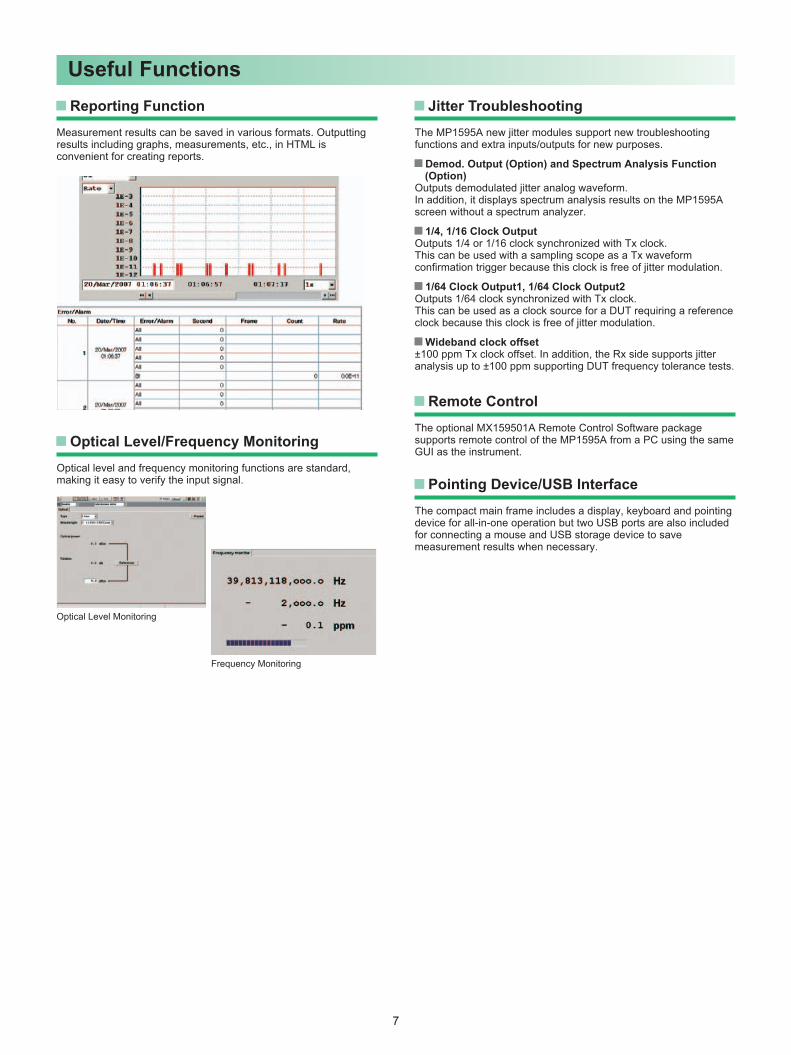
Reporting FunctionMeasurement results can be saved in various formats. Outputting results including graphs, measurements, etc., in HTML is convenient for creating reports.
Optical Level/Frequency MonitoringOptical level and frequency monitoring functions are standard, making it easy to verify the input signal.
Remote ControlThe optional MX159501A Remote Control Software package supports remote control of the MP1595A from a PC using the same GUI as the instrument.
Jitter TroubleshootingThe MP1595A new jitter modules support new troubleshooting functions and extra inputs/outputs for new purposes.
Demod. Output (Option) and Spectrum Analysis Function (Option)
Outputs demodulated jitter analog waveform.In addition, it displays spectrum analysis results on the MP1595A screen without a spectrum analyzer.
1/4, 1/16 Clock OutputOutputs 1/4 or 1/16 clock synchronized with Tx clock.This can be used with a sampling scope as a Tx waveform confirmation trigger because this clock is free of jitter modulation.
1/64 Clock Output1, 1/64 Clock Output2Outputs 1/64 clock synchronized with Tx clock.This can be used as a clock source for a DUT requiring a reference clock because this clock is free of jitter modulation.
Wideband clock offset±100 ppm Tx clock offset. In addition, the Rx side supports jitter analysis up to ±100 ppm supporting DUT frequency tolerance tests.
Pointing Device/USB InterfaceThe compact main frame includes a display, keyboard and pointing device for all-in-one operation but two USB ports are also included for connecting a mouse and USB storage device to save measurement results when necessary.
Useful Functions
8
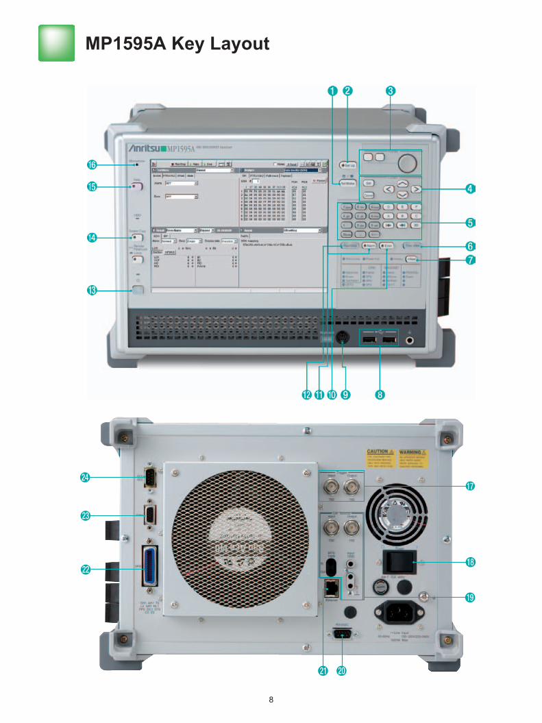
MP1595A Key Layout
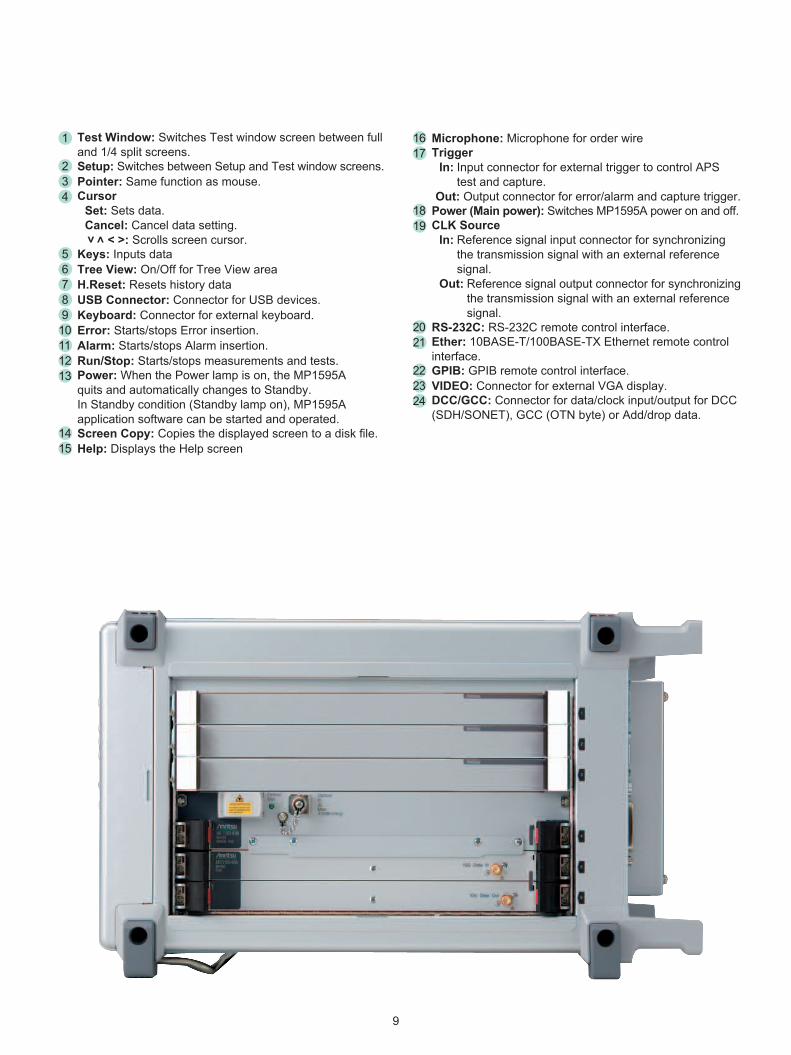
9
16 Microphone: Microphone for order wire17 Trigger
In: Input connector for external trigger to control APS test and capture.
Out: Output connector for error/alarm and capture trigger.18 Power (Main power): Switches MP1595A power on and off.19 CLK Source
In: Reference signal input connector for synchronizing the transmission signal with an external reference signal.
Out: Reference signal output connector for synchronizing the transmission signal with an external reference signal.
20 RS-232C: RS-232C remote control interface.21 Ether: 10BASE-T/100BASE-TX Ethernet remote control
interface.22 GPIB: GPIB remote control interface.23 VIDEO: Connector for external VGA display.24 DCC/GCC: Connector for data/clock input/output for DCC
(SDH/SONET), GCC (OTN byte) or Add/drop data.
1 Test Window: Switches Test window screen between full and 1/4 split screens.
2 Setup: Switches between Setup and Test window screens.3 Pointer: Same function as mouse.4 Cursor
Set: Sets data.Cancel: Cancel data setting.
< > < >: Scrolls screen cursor.5 Keys: Inputs data6 Tree View: On/Off for Tree View area7 H.Reset: Resets history data8 USB Connector: Connector for USB devices.9 Keyboard: Connector for external keyboard.
10 Error: Starts/stops Error insertion.11 Alarm: Starts/stops Alarm insertion.12 Run/Stop: Starts/stops measurements and tests.13 Power: When the Power lamp is on, the MP1595A
quits and automatically changes to Standby. In Standby condition (Standby lamp on), MP1595A application software can be started and operated.
14 Screen Copy: Copies the displayed screen to a disk file.15 Help: Displays the Help screen
10
Specifications MP1595A 40G SDH/SONET Analyzer
Clock Source Input
FrequencyClock: 1.544 MHz, 2.048 MHz, 64 kHz + 8 kHz, 5 MHz, 10 MHz Data: 1.544 Mbit/s (BITS), 2.048 Mbit/s
Input Range: ±50 ppm Level/Code
1.544 Mbit/s: ANSI T1.403 (B8ZS) 2.048 Mbit/s: ITU-T G.703 Table7 (HDB3) 1.544 MHz, 2.048 MHz, 5 MHz, 10 MHz: TTL (Rectangle, Sine Wave) 64 kHz + 8 kHz: 0.63 to 1.1 Vo-p (AMI, 8 kHz violation)
Connector1.544 MHz, 2.048 MHz, 2.048 Mbit/s, 5 MHz, 10 MHz: BNC (75 Ω) 2.048 MHz, 2.048 Mbit/s, 64 kHz + 8 kHz: SIEMENS (120 Ω) 1.544 Mbit/s: BANTAM (100 Ω)
Effective SDH/SONET/OTN Bit Rate
Clock Source Output
FrequencyClock: 1.544 MHz, 2.048 MHz, 5 MHz, 10 MHz Data: 1.544 Mbit/s (BITS), 2.048 Mbit/s
Level/Code1.544 Mbit/s: ANSI T1.403 (B8ZS) 2.048 Mbit/s: ITU-T G.703 Table10 (HDB3) 1.544 MHz, 2.048 MHz, 5 MHz, 10 MHz: TTL (Rectangle)
Connector1.544 MHz, 2.048 MHz, 2.048 Mbit/s, 5 MHz, 10 MHz: BNC (75 Ω) 1.544 Mbit/s: BANTAM (100 Ω)
Effective SDH/SONET/OTN Bit Rate
Trigger
Trigger Input: For Capture/APS Measurement Trigger Output: Transmit Error/Alarm, Receive Error/Alarm, Capture Trigger Level: TTL (Active High) Connector: BNC (75 Ω)
DCC/GCC
Data Input/Output: D1-D3 (192 kbit/s), D4-D12 (576 kbit/s), GCC0-2 (13124 kbit/s, 326.7 kbit/s) Clock Output: 192 kHz , 576 kHz, 13124 kHz, 326.7 kHz Level: V.11 Connector: D-sub 9 pin
Remote Control Remote control using LAN (10BASE-T/100BASE-TX) with MX159501A Remote command control with RS-232C (MP1595A-01) or GPIB (MP1595A-02) or LAN (MP1595A-03)
Peripheral Connection VGA Output (SVGA), USB (2 port, Rev. 1.1), Keyboard (PS/2)Pointing Device Moves cursor on screen using mouse, etc.Display Size 8.4-inch, Color TFT (800 × 600)
LEDOTN: Frame, OTU, ODU, OPU, ODTU SDH/SONET: Frame, MS/Line, AU/Path, TU/VT Standby, HDD, Clock Loss, Power Fail, History, Signal Loss, Errors, Test Pattern, PDH/DSn, Event
EMC EN61326-1, EN61000-3-2LVD EN61010-1Power and Power Consumption
100 V (ac) to 120 V (ac) / 200 V (ac) to 240 V (ac) (100/200 V system automatic change), 50 Hz / 60 Hz ≤500 VA
Operational Temperature and Humidity 5˚ to 40˚C, 20 to 80%
Dimensions and Mass 320 (W) × 221 (H) × 350 (D) mm, ≤14 kg (without plug-in units)
11
MU150140A 40/43G UnitFrame 39,813.12 Mbit/s: SDH/SONETNo Frame 39,813.12 Mbit/s
Test Pattern
PRBS (SDH/SONET)No Frame: 27 – 1, 215 – 1, 223 – 1, 231 – 1 SDH/SONET Mapping: 215 – 1, 223 – 1, 231 – 1 PDH Mapping: 211 – 1, 220 – 1, 220 – 1z Invert On/Off
Word:VC4 × 256c: 32-bit Programmable (including All 0, All 1) Others: 16-bit Programmable (including All 0, All 1)
OH Preset SOH/TOH/POH: All Bytes (except Parity Byte, K1/K2 Byte, H1, H2 and H3) Dummy Channel POH: All Bytes (except Parity Byte)
Error Addition/Measurement
<SDH> Bit all, FAS, B1, B2, MS-REI (M0/M1), HP-B3, HP-REI, HP-IEC, HP-TC-REI, HP-OEI, LP-B3, BIP-2, LP-REI, LP-IEC, N2-BIP-2, LP-TC-REI, LP-OEI Bit info<SONET> Bit all, FAS, B1, B2, REI-L (M0/M1), B3-P, REI-P, IEC-P, TC-REI-P, OEI-P, B3-V, BIP-2, REI-V, IEC-V, Z6-BIP-2, TC-REI-V, OEI-V Bit info
Error Addition Timing
Rate, Alternative, Single, Burst, All, Frame Rate
Fix Rate: 1 × 10–n (n: 3 to 9), User Program: A × 10–B (A: 1.0 to 9.9/0.1 step, B: 2 to 10) Alternative
Error Frame: 0 to 64000, Normal Frame: 1 to 64000 Frame (only PDH/DSn): n in 16 Frame (n: 1 to 4) B1, B2, B3, BIP-2 set as Error Bit.
Alarm Addition/Measurement
<SDH> LOF, RS-TIM (Timing: All only), MS-AIS, MS-RDI, AU-AIS, AU-LOP, HP-SLM, HP-TIM (Timing: All only), HP-RDI, HP-UNEQ, HP-ERDIP, HP-ERDIS, HP-ERDIC, HP-VC-AIS, HP-Incoming AIS, HP-TC-RDI, HP-ODI, HP-TCUNEQ, HP-TCTIM (Timing: All only), HP-LTC, TU-AIS, TU-LOP, TU-LOM, LP-SLM, LP-TIM (Timing: All only), LP-RDI, LP-UNEQ, LP-ERDIP, LP-ERDIS, LP-ERDIC, LP-RFI, LP-VC-AIS, LP-Incoming AIS, LP-TC-RDI, LP-ODI, LP-TCUNEQ, LP-TCTIM (Timing: All only), LP-LTC <SONET> LOF, RS-TIM (Timing: All only), AIS-L, RDI-L, AIS-P, LOP-P, SLM-P, TIM-P (Timing: All only), RDI-P, UNEQ-P, ERDIP-P, ERDIS-P, ERDIC-P, STS-VC-AIS, Incoming AIS-P, TC-RDI-P, ODI-P, TCUNEQ-P, TCTIM-P (Timing: All only), LTC-P, AIS-V, LOP-V, LOM-V, SLM-V, TIM-V (Timing: All only), RDI-V, UNEQ-V, ERDIP-V, ERDIS-V, ERDIC-V, RFI-V, VC-AIS-V, Incoming AIS-V, TC-RDI-V, ODI-V, TCUNEQ-V, TCTIM-V (Timing: All only), LTC-V
Alarm Addition TimingSingle, Burst, Alternative, All Alternative
Error Frame: 0 to 64000, Normal Frame: 1 to 64000
10G Date Input
Bit Rate: 9,953.28 Mbit/s ±30 ppm Code: NRZ Connector: SMA 50 Ω Level: 0.3 to 1.5 Vp-p
10G Date Output
Bit Rate: 9,953.28 Mbit/s Code: NRZ Connector: SMA 50 Ω Level: 0.71 Vp-p ±0.08 V
Clock
Internal, Receive Internal
Accuracy: ±2 ppm [After Power On, Calibrate after 24 Hours, Warm-up 23 ±5˚C, Aging Rate (Max.): ±0.05 ppm/day, ±0.5 ppm/year]
Offset Range: ±30 ppm, Step: 0.1 ppmMonitor SDH/SONET: SOH/TOH/POH, Path Trace, Tandem Byte, K1/K2 Byte, AU/STS, TU/VT PointerThrough Transparent, Overhead Overwrite (Only SDH/SONET/OTN)
Delay Measurement Measurement Period: 0.5, 1, 2, 5, 10 s Measurement Range: 0 to 999 µs (1 µs step), 1.0 ms to 999.9 ms (0.1 ms step), 1.0 s to 10.0 s (0.1 s step), >Time Out
Dummy Channel Mode: Copy/Dummy Dummy Pattern: All 0, All 1, 211 – 1, 215 – 1 (Invert)
Path Trace J0, J1, J2 Byte can be set arbitrarily. 16 byte (CRC On), 64 byte (CRC Off, J1 Only)
Tandem Connection N1/Z5, N2 Byte can be set arbitrarily. It can set On/Off
Pointer Generation
AU/STS, TU/VT Pointer Action: NDF, ±PJ (Pointer Justification), Inc./Dec. PJC Timing: Manual, Burst (2 to 64) Inc./Dec. Timing: 4 to 8000 Frame
APS TestTrigger: B1, B2, HP-B3, LP-B3, BIP-2, MS-AIS/AIS-L, AU-AIS/AIS-P, TU-AIS/AIS-V, BIT, External Range: 2 s Step: 0.1 ms
12
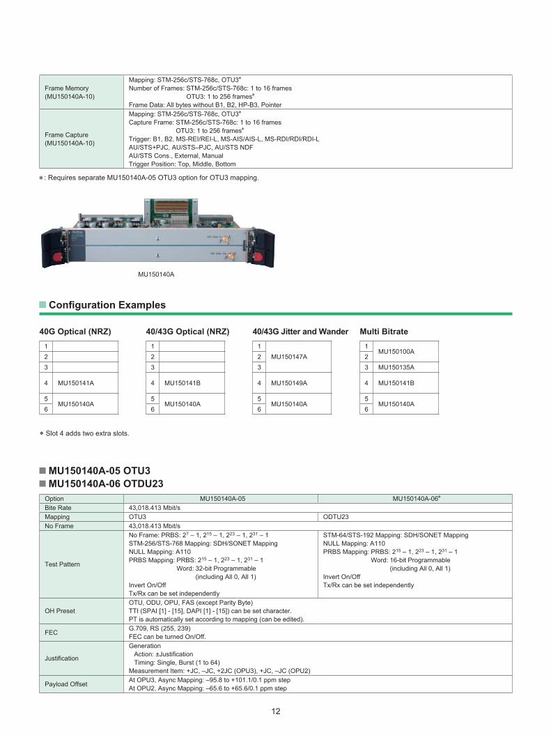
MU150140A
Configuration Examples
• Slot 4 adds two extra slots.
MU150140A-05 OTU3 MU150140A-06 OTDU23Option MU150140A-05 MU150140A-06∗
Bite Rate 43,018.413 Mbit/sMapping OTU3 ODTU23No Frame 43,018.413 Mbit/s
Test Pattern
No Frame: PRBS: 27 – 1, 215 – 1, 223 – 1, 231 – 1 STM-256/STS-768 Mapping: SDH/SONET Mapping NULL Mapping: A110 PRBS Mapping: PRBS: 215 – 1, 223 – 1, 231 – 1
Word: 32-bit Programmable (including All 0, All 1)
Invert On/Off Tx/Rx can be set independently
STM-64/STS-192 Mapping: SDH/SONET Mapping NULL Mapping: A110 PRBS Mapping: PRBS: 215 – 1, 223 – 1, 231 – 1
Word: 16-bit Programmable (including All 0, All 1)
Invert On/Off Tx/Rx can be set independently
OH PresetOTU, ODU, OPU, FAS (except Parity Byte) TTI (SPAI [1] - [15], DAPI [1] - [15]) can be set character. PT is automatically set according to mapping (can be edited).
FEC G.709, RS (255, 239) FEC can be turned On/Off.
Justification
Generation Action: ±Justification Timing: Single, Burst (1 to 64)
Measurement Item: +JC, –JC, +2JC (OPU3), +JC, –JC (OPU2)
Payload Offset At OPU3, Async Mapping: –95.8 to +101.1/0.1 ppm step At OPU2, Async Mapping: –65.6 to +65.6/0.1 ppm step
40G Optical (NRZ)123
4 MU150141A
5MU150140A
6
40/43G Optical (NRZ)123
4 MU150141B
5MU150140A
6
40/43G Jitter and Wander1
MU150147A23
4 MU150149A
5MU150140A
6
Multi Bitrate1
MU150100A23 MU150135A
4 MU150141B
5MU150140A
6
Frame Memory (MU150140A-10)
Mapping: STM-256c/STS-768c, OTU3∗ Number of Frames: STM-256c/STS-768c: 1 to 16 frames
OTU3: 1 to 256 frames∗Frame Data: All bytes without B1, B2, HP-B3, Pointer
Frame Capture (MU150140A-10)
Mapping: STM-256c/STS-768c, OTU3∗ Capture Frame: STM-256c/STS-768c: 1 to 16 frames
OTU3: 1 to 256 frames∗Trigger: B1, B2, MS-REI/REI-L, MS-AIS/AIS-L, MS-RDI/RDI/RDI-L AU/STS+PJC, AU/STS–PJC, AU/STS NDF AU/STS Cons., External, Manual Trigger Position: Top, Middle, Bottom
∗: Requires separate MU150140A-05 OTU3 option for OTU3 mapping.
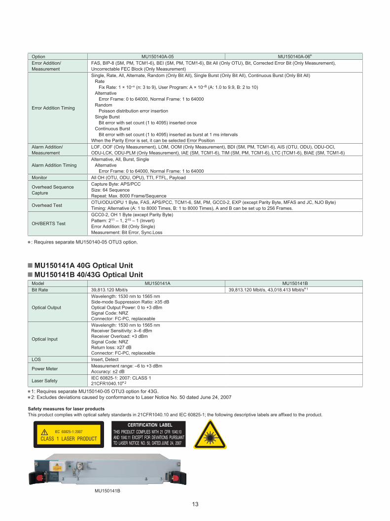
13
Option MU150140A-05 MU150140A-06∗
Error Addition/Measurement
FAS, BIP-8 (SM, PM, TCM1-6), BEI (SM, PM, TCM1-6), Bit All (Only OTU), Bit, Corrected Error Bit (Only Measurement), Uncorrectable FEC Block (Only Measurement)
Error Addition Timing
Single, Rate, All, Alternate, Random (Only Bit All), Single Burst (Only Bit All), Continuous Burst (Only Bit All)Rate Fix Rate: 1 × 10–n (n: 3 to 9), User Program: A × 10–B (A: 1.0 to 9.9, B: 2 to 10)Alternative Error Frame: 0 to 64000, Normal Frame: 1 to 64000Random Poisson distribution error insertionSingle Burst Bit error with set count (1 to 4095) inserted onceContinuous Burst Bit error with set count (1 to 4095) inserted as burst at 1 ms intervals
When the Parity Error is set, it can be selected Error PositionAlarm Addition/Measurement
LOF, OOF (Only Measurement), LOM, OOM (Only Measurement), BDI (SM, PM, TCM1-6), AIS (OTU, ODU), ODU-OCI, ODU-LCK, ODU-PLM (Only Measurement), IAE (SM, TCM1-6), TIM (SM, PM, TCM1-6), LTC (TCM1-6), BIAE (SM, TCM1-6)
Alarm Addition TimingAlternative, All, Burst, Single
Alternative Error Frame: 0 to 64000, Normal Frame: 1 to 64000
Monitor All OH (OTU, ODU, OPU), TTI, FTFL, Payload
Overhead Sequence Capture
Capture Byte: APS/PCC Size: 64 Sequence Repeat: Max. 8000 Frame/Sequence
Overhead Test OTU/ODU/OPU 1 Byte, FAS, APS/PCC, TCM1-6, SM, PM, GCC0-2, EXP (except Parity Byte, MFAS and JC, NJO Byte) Timing: Alternative (A: 1 to 8000 Times, B: 1 to 8000 Times), A and B can be set up to 256 Frames.
OH/BERTS Test
GCC0-2, OH 1 Byte (except Parity Byte) Pattern: 211 – 1, 215 – 1 (Invert) Error Addition: Bit (Only Single) Measurement: Bit Error, Sync.Loss
∗: Requires separate MU150140-05 OTU3 option.
MU150141A 40G Optical Unit MU150141B 40/43G Optical UnitModel MU150141A MU150141BBit Rate 39,813.120 Mbit/s 39,813.120 Mbit/s, 43,018.413 Mbit/s∗1
Optical Output
Wavelength: 1530 nm to 1565 nm Side-mode Suppression Ratio: ≥35 dB Optical Output Power: 0 to +3 dBm Signal Code: NRZ Connector: FC-PC, replaceable
Optical Input
Wavelength: 1530 nm to 1565 nm Receiver Sensitivity: ≥–6 dBm Receiver Overload: +3 dBm Signal Code: NRZ Return loss: ≥27 dB Connector: FC-PC, replaceable
LOS Insert, Detect
Power Meter Measurement range: –6 to +3 dBm Accuracy: ±2 dB
Laser Safety IEC 60825-1: 2007: CLASS 121CFR1040.10∗2
∗1: Requires separate MU150140-05 OTU3 option for 43G.∗2: Excludes deviations caused by conformance to Laser Notice No. 50 dated June 24, 2007
Safety measures for laser productsThis product complies with optical safety standards in 21CFR1040.10 and IEC 60825-1; the following descriptive labels are affixed to the product.
MU150141B
14
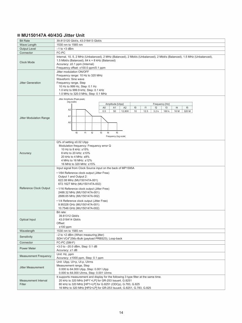
MU150147A 40/43G Jitter UnitBit Rate 39.813120 Gbit/s, 43.018413 Gbit/sWave Length 1530 nm to 1565 nmOutput Level –1 to +3 dBmConnector FC-PC
Clock Mode
Internal, 10, 5, 2 MHz (Unbalanced), 2 MHz (Balanced), 2 Mbit/s (Unbalanced), 2 Mbit/s (Balanced), 1.5 MHz (Unbalanced), 1.5 Mbit/s (Balanced), 64 k + 8 kHz (Balanced)Accuracy: ±0.1 ppm (Internal)Frequency offset: ±100.0 ppm/0.1 ppm
Jitter Generation
Jitter modulation ON/OFFFrequency range: 10 Hz to 320 MHzWaveform: Sine waveFrequency range, Step
10 Hz to 999 Hz, Step: 0.1 Hz1.0 kHz to 999.9 kHz, Step: 0.1 kHz1.0 MHz to 320.0 MHz, Step: 0.1 MHz
Jitter Modulation Range
Accuracy
Q% of setting ±0.02 UIppModulation frequency: Frequency error Q
10 Hz to 8 kHz: ±15%8 kHz to 20 kHz: ±10%20 kHz to 4 MHz: ±8%4 MHz to 16 MHz: ±12%16 MHz to 320 MHz: ±15%
Reference Clock Output
Input signal from Clock Source input on the back of MP1595A
• 1/64 Reference clock output (Jitter Free) Output 1 and Output 2: 622.08 MHz (MU150147A-001) 672.1627 MHz (MU150147A-002)
• 1/16 Reference clock output (Jitter Free) 2488.32 MHz (MU150147A-001) 2688.65 MHz (MU150147A-002)
• 1/4 Reference clock output (Jitter Free) 9.95328 GHz (MU150147A-001) 10.7546 GHz (MU150147A-002)
Optical Input
Bit rate:39.81312 Gbit/s43.018414 Gbit/s
Offset:±100 ppm
Wavelength 1530 nm to 1565 nm
Sensitivity –2 to +2 dBm (When measuring jitter)SDH VC4∗256c-Bulk (payload PRBS23), Loop-back
Connector FC-PC (SM-F)
Power Meter +3.0 to –20.0 dBm, Step: 0.1 dBAccuracy: ±1 dB
Measurement Frequency Unit: Hz, ppmAccuracy: ±1000 ppm, Step: 0.1 ppm
Jitter Measurement
Unit: UIpp, UI+p, UI-p, UIrmsMeasurement range, Step
0.000 to 64.000 UIpp, Step: 0.001 UIpp0.000 to 64.000 UIrms, Step: 0.001 UIrms
Measurement Interval Filter
It supports measurement and display for the following 3 type filter at the same time.20 kHz to 320 MHz [HP1’+LP] for GR-253 Issue4, G.825180 kHz to 320 MHz [HP1+LP] for G.8251 (ODCp), G.783, G.82516 MHz to 320 MHz [HP2+LP] for GR-253 Isuue4, G.8251, G.783, G.825
Amplitude [UIpp] Frequency [Hz]A0 A1 A2 f0 f1 f2 f3 f4 f50.5 50 12,800 10 12.5 3.2 k 160 k 16 M 320 M
15
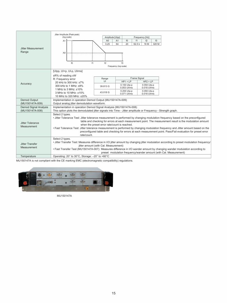
MU150147A
Jitter Measurement Range
Accuracy
[UIpp, UI+p, UI-p, UIrms]
±R% of reading ±WR: Frequency error
20 kHz to 300 kHz: ±7%300 kHz to 1 MHz: ±8%1 MHz to 3 MHz: ±10%3 MHz to 10 MHz: ±15%10 MHz to 320 MHz: ±20%
Demod Output(MU150147A-009)
Implementation in operation Demod Output (MU150147A-009)Output analog jitter demodulation waveform.
Demod Signal Analysis (MU150147A-008)
Implementation in operation Demod Signal Analysis (MU150147A-008)This option plots the demodulated jitter signals into Time - Jitter amplitude or Frequency - Strength graph.
Jitter Tolerance Measurement
Select 2 types.• Jitter Tolerance Test: Jitter tolerance measurement is performed by changing modulation frequency based on the preconfigured
table and checking for errors at each measurement point. The measurement result is the modulation amount when the preset error rate/count is reached.
• Fast Tolerance Test: Jitter tolerance measurement is performed by changing modulation frequency and Jitter amount based on the preconfigured table and checking for errors at each measurement point. Pass/Fail evaluation for preset error rate/count.
Jitter Transfer Measurement
Select 2 types.• Jitter Transfer Test: Measures difference in I/O jitter amount by changing jitter modulation according to preset modulation frequency/
jitter amount (with Cal. Measurement)• Fast Transfer Test (MU150147A-007): Measures difference in I/O wander amount by changing wander modulation according to
preset modulation frequency/wander amount (with Cal. Measurement) Temperature Operating: 20° to 30°C, Storage: –20° to +60°C
MU150147A is not compliant with the CE marking EMC (electromagnetic compatibility) regulations.
RangeUI
Frame SignalHP1 + LP HP2 + LP
39.813 G 0.150 UIp-p0.053 UIrms
0.050 UIp-p0.018 UIrms
43.018 G 0.200 UIp-p0.071 UIrms
0.050 UIp-p0.018 UIrms
Amplitude [UIpp] Frequency [Hz]A0 A1 f0 f1 f2 f3
0.25 64 20 62.5 k 16 M 320 M
16
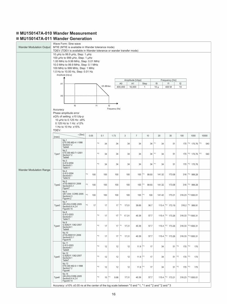
MU150147A-010 Wander Measurement MU150147A-011 Wander Generation
Wander Modulation OutputWave Form: Sine waveMTIE (MTIE is available in Wander tolerance mode)TDEV (TDEV is available in Wander tolerance or wander transfer mode)
Wander Modulation Range
10 µHz to 99.9 µHz, Step: 1 µHz100 µHz to 999 µHz, Step: 1 µHz1.00 MHz to 9.99 MHz, Step: 0.01 MHz10.0 MHz to 99.9 MHz, Step: 0.1 MHz100 MHz to 999 MHz, Step: 1 MHz1.0 Hz to 10.00 Hz, Step: 0.01 Hz
AccuracyPhase amplitude error±Q% of setting: ±10 UIp-p
10 µHz to 0.125 Hz: ±8%0.125 Hz to 1 Hz: ±12%1 Hz to 10 Hz: ±15%
TDEV:
Accuracy: ±10% ±0.05 ns at the center of the log scale between ∗0 and ∗1, ∗1 and ∗2 and ∗2 and ∗3
Amplitude [UIpp] Frequency [Hz]A0 A1 Step f0 f1 f2
400,000 16,000 1 10 µ 400 M 10
τ [Sec][nsec] 0.05 0.1 1.73 3 7 10 20 30 100 1000 10000
Type1
No.1ETS 300 462-4-1-1998Section7.2Table6
∗0 34 34 34 34 34 ∗1 34 51 170 ∗2 170.76 ∗3 540
No.2ETS 300 462-7-1-2001Section7.2Table6
∗0 34 34 34 34 34 ∗1 34 51 170 ∗2 170.76 ∗3 540
No.3G.812-2004Section9.1Table11
∗0 34 34 34 34 34 ∗1 34 51 170 ∗2 170.76
Type2
No.4G.812-2004Section9.1Table12
∗0 100 100 100 100 100 ∗1 99.93 141.32 173.08 316 ∗3 999.28
No.5ATIS-0900101.2006Section8.5.1Figure7
∗0 100 100 100 100 100 ∗1 99.93 141.32 173.08 316 ∗3 999.28
No.6GR-1244- CORE-2005Section4.3Figure4.2
∗0 100 100 100 100 100 ∗1 100 141.42 173.21 316.23 ∗2 1000.01
Type3No.7GR-253-CORE-2005Section5.4.4.2.4Figure5-15
∗0 17 17 17 ∗1 17.01 39.69 56.7 113.4 ∗2 173.19 316.2 ∗3 999.91
Type4
No.8G.813-2003Section8.1Table11
∗0 17 17 ∗1 17.31 40.39 57.7 115.4 ∗2 173.26 316.33 ∗3 1000.31
No.9G.8262/Y.1362-2007Section9.1Table9
∗0 17 17 ∗1 17.31 40.39 57.7 115.4 ∗2 173.26 316.33 ∗3 1000.31
No.10ATIS-0900101.2006Section8.5.1Figure16
∗0 17 17 ∗1 17.31 40.39 57.7 115.4 ∗2 173.26 316.33 ∗3 1000.31
Type5
No.11G.813-2003Section8.1Table9
∗0 12 12 12 11.9 ∗1 17 34 51 ∗2 170 ∗3 170
No.12G.8262/Y.1362-2007Section9.1Table7
∗0 12 12 12 11.9 ∗1 17 34 51 ∗2 170 ∗3 170
No.13ETS 300 462-5-1-1998Section7.2Figure6
∗0 12 12 12 11.9 ∗1 17 34 51 ∗2 170 ∗3 170
Type6No.14GR-253-CORE-2005Section5.4.4.2.4Figure5-14
∗0 10 ∗1 9.98 17.31 40.39 57.7 115.4 ∗2 173.21 316.23 ∗3 1000.01
17
Wander Measurement
Measurement range: 0 to ±1E10 ns (deviation within 1 s must be within ±500 ppm)Observation time: 12, 120, 1,200, 12,000, 120,000 sSampling rate: 40 samples/s (Conforms to ITU-T O.172/O.173 Recommendation)Display result: TIE, MTIE, TDEV
Wander Tolerance Measurement
Type: TDEV Tolerance, MTIE ToleranceMask
G.812-2004 Section9.1 Table11, Table12G.813-2003 Section8.1 Table9, Table11G.8262/Y.1362-2007 Section9.1 Table7, Table9ETS 300 462-4-1-1998 Section7.2 Table6ETS 300 462-5-1-1998 Section7.2 Table6ETS 300 462-7-1-2001 Section7.2 Table6GR-1244-CORE-2005 Section4.3 Figure4.2GR-253-CORE-2005 Section5.4.4.2.4 Figure5-14, Figure5-15
Wander Transfer Measurement
Type: TDEV TransferMask
G.812-2004 Section10 Table18, Table19G.813-2003 Section9 Table13G.8262/Y.1362-2007 Section10 Table10ETS 300 462-4-1-1998 Section8 Table9ETS 300 462-7-1-2001 Section8 Table9GR-1244-CORE-2005 Section5.4 Figure5-6GR-253-CORE-2005 Section5.4.4.2.4 Figure5-14, Figure5-14
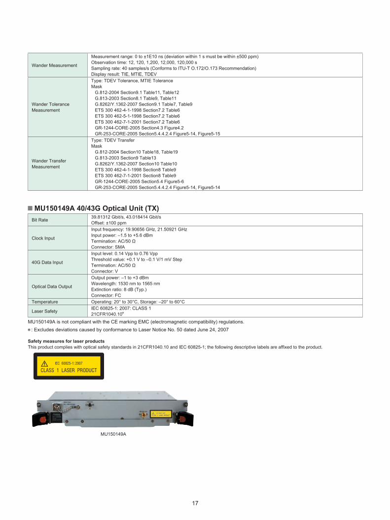
MU150149A 40/43G Optical Unit (TX)Bit Rate 39.81312 Gbit/s, 43.018414 Gbit/s
Offset: ±100 ppm
Clock Input
Input frequency: 19.90656 GHz, 21.50921 GHzInput power: –1.5 to +5.6 dBmTermination: AC/50 ΩConnector: SMA
40G Data Input
Input level: 0.14 Vpp to 0.76 VppThreshold value: +0.1 V to –0.1 V/1 mV StepTermination: AC/50 ΩConnector: V
Optical Data Output
Output power: –1 to +3 dBmWavelength: 1530 nm to 1565 nmExtinction ratio: 8 dB (Typ.)Connector: FC
Temperature Operating: 20° to 30°C, Storage: –20° to 60°C
Laser Safety IEC 60825-1: 2007: CLASS 121CFR1040.10∗
MU150149A is not compliant with the CE marking EMC (electromagnetic compatibility) regulations.
∗: Excludes deviations caused by conformance to Laser Notice No. 50 dated June 24, 2007
Safety measures for laser productsThis product complies with optical safety standards in 21CFR1040.10 and IEC 60825-1; the following descriptive labels are affixed to the product.
MU150149A
18
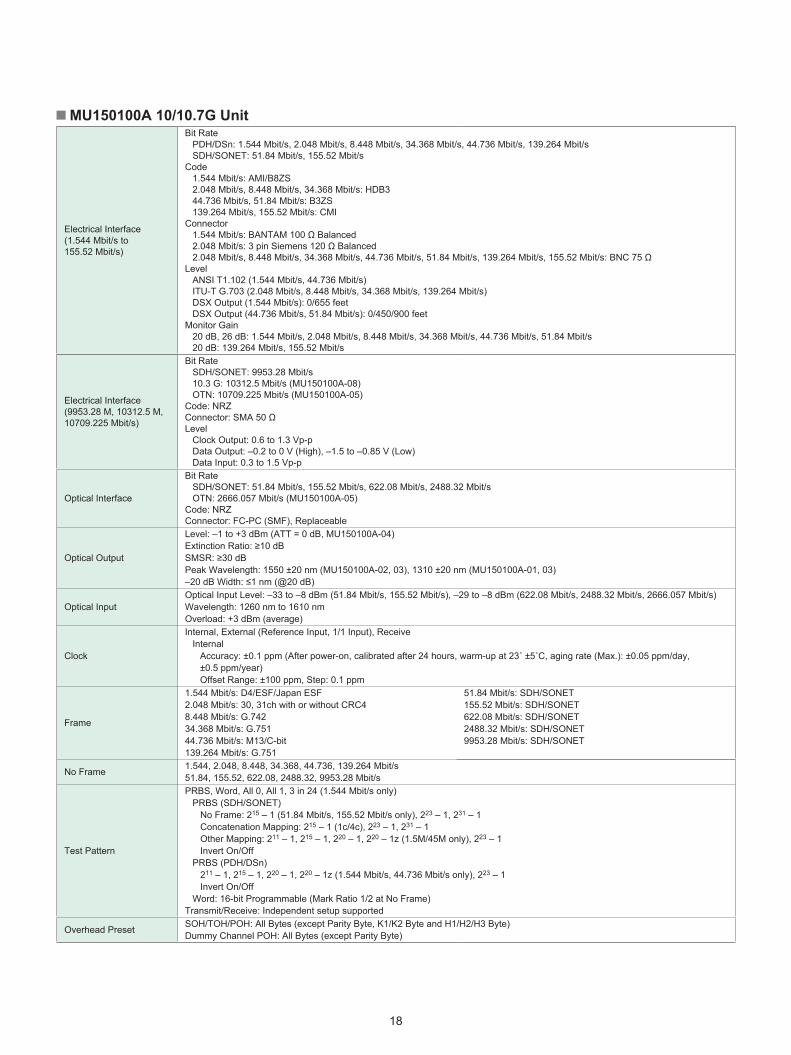
MU150100A 10/10.7G Unit
Electrical Interface(1.544 Mbit/s to 155.52 Mbit/s)
Bit RatePDH/DSn: 1.544 Mbit/s, 2.048 Mbit/s, 8.448 Mbit/s, 34.368 Mbit/s, 44.736 Mbit/s, 139.264 Mbit/sSDH/SONET: 51.84 Mbit/s, 155.52 Mbit/s
Code1.544 Mbit/s: AMI/B8ZS2.048 Mbit/s, 8.448 Mbit/s, 34.368 Mbit/s: HDB344.736 Mbit/s, 51.84 Mbit/s: B3ZS139.264 Mbit/s, 155.52 Mbit/s: CMI
Connector1.544 Mbit/s: BANTAM 100 Ω Balanced2.048 Mbit/s: 3 pin Siemens 120 Ω Balanced2.048 Mbit/s, 8.448 Mbit/s, 34.368 Mbit/s, 44.736 Mbit/s, 51.84 Mbit/s, 139.264 Mbit/s, 155.52 Mbit/s: BNC 75 Ω
Level ANSI T1.102 (1.544 Mbit/s, 44.736 Mbit/s)ITU-T G.703 (2.048 Mbit/s, 8.448 Mbit/s, 34.368 Mbit/s, 139.264 Mbit/s)DSX Output (1.544 Mbit/s): 0/655 feetDSX Output (44.736 Mbit/s, 51.84 Mbit/s): 0/450/900 feet
Monitor Gain20 dB, 26 dB: 1.544 Mbit/s, 2.048 Mbit/s, 8.448 Mbit/s, 34.368 Mbit/s, 44.736 Mbit/s, 51.84 Mbit/s20 dB: 139.264 Mbit/s, 155.52 Mbit/s
Electrical Interface(9953.28 M, 10312.5 M, 10709.225 Mbit/s)
Bit RateSDH/SONET: 9953.28 Mbit/s10.3 G: 10312.5 Mbit/s (MU150100A-08)OTN: 10709.225 Mbit/s (MU150100A-05)
Code: NRZConnector: SMA 50 ΩLevel
Clock Output: 0.6 to 1.3 Vp-pData Output: –0.2 to 0 V (High), –1.5 to –0.85 V (Low)Data Input: 0.3 to 1.5 Vp-p
Optical Interface
Bit RateSDH/SONET: 51.84 Mbit/s, 155.52 Mbit/s, 622.08 Mbit/s, 2488.32 Mbit/sOTN: 2666.057 Mbit/s (MU150100A-05)
Code: NRZConnector: FC-PC (SMF), Replaceable
Optical Output
Level: –1 to +3 dBm (ATT = 0 dB, MU150100A-04)Extinction Ratio: ≥10 dBSMSR: ≥30 dBPeak Wavelength: 1550 ±20 nm (MU150100A-02, 03), 1310 ±20 nm (MU150100A-01, 03)–20 dB Width: ≤1 nm (@20 dB)
Optical InputOptical Input Level: –33 to –8 dBm (51.84 Mbit/s, 155.52 Mbit/s), –29 to –8 dBm (622.08 Mbit/s, 2488.32 Mbit/s, 2666.057 Mbit/s)Wavelength: 1260 nm to 1610 nmOverload: +3 dBm (average)
Clock
Internal, External (Reference Input, 1/1 Input), ReceiveInternal
Accuracy: ±0.1 ppm (After power-on, calibrated after 24 hours, warm-up at 23˚ ±5˚C, aging rate (Max.): ±0.05 ppm/day, ±0.5 ppm/year) Offset Range: ±100 ppm, Step: 0.1 ppm
Frame
1.544 Mbit/s: D4/ESF/Japan ESF2.048 Mbit/s: 30, 31ch with or without CRC48.448 Mbit/s: G.74234.368 Mbit/s: G.75144.736 Mbit/s: M13/C-bit139.264 Mbit/s: G.751
51.84 Mbit/s: SDH/SONET 155.52 Mbit/s: SDH/SONET 622.08 Mbit/s: SDH/SONET 2488.32 Mbit/s: SDH/SONET 9953.28 Mbit/s: SDH/SONET
No Frame 1.544, 2.048, 8.448, 34.368, 44.736, 139.264 Mbit/s 51.84, 155.52, 622.08, 2488.32, 9953.28 Mbit/s
Test Pattern
PRBS, Word, All 0, All 1, 3 in 24 (1.544 Mbit/s only)PRBS (SDH/SONET) No Frame: 215 – 1 (51.84 Mbit/s, 155.52 Mbit/s only), 223 – 1, 231 – 1 Concatenation Mapping: 215 – 1 (1c/4c), 223 – 1, 231 – 1 Other Mapping: 211 – 1, 215 – 1, 220 – 1, 220 – 1z (1.5M/45M only), 223 – 1 Invert On/OffPRBS (PDH/DSn) 211 – 1, 215 – 1, 220 – 1, 220 – 1z (1.544 Mbit/s, 44.736 Mbit/s only), 223 – 1 Invert On/OffWord: 16-bit Programmable (Mark Ratio 1/2 at No Frame)
Transmit/Receive: Independent setup supported
Overhead Preset SOH/TOH/POH: All Bytes (except Parity Byte, K1/K2 Byte and H1/H2/H3 Byte)Dummy Channel POH: All Bytes (except Parity Byte)
19
Error Addition/ Measurement
PDH/DSnBit All (Only Addition), Code, Bit Info, Bit 1.5M, Bit 2M, Bit 8M, Bit 34M, Bit 45M, Bit 139M, FAS 1.5M, FAS 2M, FAS 8M, FAS 34M, FAS 45M, FAS 139M, EXZ, CRC6, Ebit, Parity, Cbit, REI
SDHFAS, Frame (Measurement only), B1, B2, HP-B3, LP-B3, BIP-2, MS-REI (M0/M1), HP-REI, LP-REI, Bit All (Only Addition), Bit Info, OH Bit, HP-IEC, LP-IEC, N2 BIP-2, HP-TC-REI, LP-TC-REI, HP-OEI, LP-OEI
SONETFAS, Frame (Measurement only), B1, B2, HP-B3, LP-B3, BIP-2, REI-L (M0/M1), REI-P, REI-V, Bit All (Only Addition), Bit Info, OH Bit, HP-IEC, LP-IEC, N2 BIP-2, HP-TC-REI, LP-TC-REI, HP-OEI, LP-OEI
Error Addition Timing
Rate, Alternative, Single, Burst, All, FrameRate Fix Rate: 1 × 10–n (n: 3 to 9), User Program: A × 10–B (A: 1.0 to 9.9, step 0.1, B: 2 to 10)Alternative Error Frame: 0 to 64000, Normal Frame: 1 to 64000 Frame (only at PDH/DSn): Insert n Error Frames (n: 1 to 4) in 16 frames
Specify insertion bit position at B1, B2, B3, BIP-2 error insertion
Alarm Addition/ Measurement
PDH/DSn: LOS, LOF, AIS, RDI, RDI (MF)SDH: LOS, LOF, OOF (Measurement only), RS-TIM, MS-AIS, MS-RDI, AU-AIS, AU-LOP, HP-RDI, HP-ERDIP, HP-ERDIS,
HP-ERDIC, HP-TIM, HP-UNEQ, HP-SLM, TU-AIS, TU-LOP, TU-LOM, LP-RDI, LP-ERDIP, LP-ERDIS, LP-ERDIC, ISF, LP-RFI, LP-TIM, LP-UNEQ, LPSLM, Sync. loss, OH Sync., HP-VC-AIS, LP-VC-AIS, HP-FAS, LP-FAS, HP-Incoming AIS, LP-Incoming AIS, HP-TC-RDI, LPTC-RDI, HP-ODI, LP-ODI, HP-TC-TIM, LP-TC-TIM, HP-LTC, LP-LTC
SONET: LOS, LOF, OOF (Measurement only), RS-TIM, AIS-L, RDI-L, AIS-P, LOP-P, RDI-P, ERDIP-P, ERDIS-P, ERDIC-P, TIM-P, UNEQ-P, PLM-P, AIS-V, LOP-V, LOM-V, RDI-V, ERDIP-V, ERDIS-V, ERDIC-V, ISF, RFI-V, TIM-V, UNEQ-V, PLM-V, Sync. loss, OH Sync., HP-VC-AIS, LP-VC-AIS, HP-FAS, LP-FAS, HP-Incoming AIS, LP-Incoming AIS, HP-TC-RDI, LP-TC-RDI, HP-ODI, LP-ODI, HP-TC-TIM, LP-TCTIM, HP-LTC, LP-LTC
Alarm Addition TimingSingle, Burst, Alternative, AllAlternative
Error Frame: 0 to 64000, Normal Frame: 1 to 64000
Monitor PDH/DSn: FAS 1.5M, FW 2M, NFW 2M, MFW 2M, FAS 8M, FAS 34M, FAS 45M, FAS 139M, Info Byte (2M only)SDH/SONET: SOH/TOH/POH, Path Trace, Tandem Byte, K1/K2 Byte, AU/STS, TU/VT Pointer, Payload
Through Transparent, Overhead Overwrite (SDH/SONET/OTN only)MUX/DEMUX MUX/DEMUX supported to 64 k units in PDH and DSnAdd/Drop (MU150100A-09) STM-0/1/4/16 or OC-1/3/12/48 signal added to or dropped from STM-64 or OC-192 signal
Delay Measurement Measurement Period: 0.5, 1, 2, 5, 10 sMeasurement Range: 0. to 999 μs (1 µs step), 1.0 ms to 999.9 ms (0.1 ms step), 1.0 s to 10.0 s (0.1 s step), > Time Out
Dummy Channel Mode: Copy/DummyDummy Pattern: All 0, All 1, PRBS 211 – 1, PRBS 215 – 1 (Invert)
Path Trace J0, J1, J2 Byte set arbitrarily16 bytes (CRC On), 64 bytes (CRC Off, J1 only)
Tandem Connection N1/Z5, N2 Byte set arbitrarilySet On/Off
Pointer GenerationAU/STS, TU/VT Pointer
Action: NDF, ±PJ (Pointer Justification), Inc./Dec.PJC Timing: Manual, Burst (2 to 64), Inc./Dec. Timing: 4 to 8000 Frames
Pointer Measurement AU/STS, TU/VT Pointer, C BitMeasurement Item: NDF, +PJC, –PJC, Cons, C, C1/C2
Payload Offset Offset Range: ±100 ppm/0.1 ppm step set at Async Mapping
APS Test
Switching Time MeasurementMeasurement Time: 0.1 ms to 2000.0 ms, Timeout (exclude Time for Frame/Pointer Synchronization)
APS Sequence GeneratorGenerator Timing: 2 to 64 words, Max. 8000 frames/wordsSet for K1/K2, K3, K4 Byte
Overhead Sequence Capture
Capture Byte: K1/K2, K3, K4, AU/STS Pointer, TU/VT PointerSize: 64 SequenceRepeat: Max. 8000 Frame/Sequence
Overhead Test SOH/TOH/POH 1 Byte, A1/A2, K1/K2, RSOH, MSOH, SOH, POH (except Parity Byte, K1/K2 Byte and H1/H2/H3 Byte)Timing: Alternative (A: 1 to 8000 Times, B: 1 to 8000 Times), A and B can be set up to 256 frames.
Overhead BERT Test
Test Byte: SOH/TOH/POH 1 Byte, D1-D3, D4-D12 (except Parity Byte, K1/K2 Byte and H1/H2/H3 Byte)Pattern: PRBS 211 – 1, PRBS 215 – 1 (Invert)Error Addition: Bit (Only Single)Measurement: Bit Error, Sync Loss
Overhead Add/Drop Test Byte: D1-D3, D4-D12Error Performance G.821, G.826, G.828, G.829, M.2100, M.2101, M.2110, M.2120, GR.820
Optical Power MeterWavelength: 1310 nm/1550 nmMeasurement Range: –40 to –7 dBmMeasurement Accuracy: ±1 dB (–30 to –10 dBm), ±2 dB (–9.9 to –7 dBm, –40 to –30.1 dBm)
Frequency Counter
Measurement Frequency (f0):1.544, 2.048, 8.448, 34.368, 44.736, 51.84, 139.264, 155.52, 622.08, 2488.320, 2666.057, 9953.28, 10709.225 MHz
Measurement Range: f0 ±100 ppmAccuracy: ±0.1 ppm
Auxiliary Interface External Clock Input, Receive Clock Output, Clock/Frame Sync. Output
20
MU150100A-05 OTU1/OTU2Bite Rate 10709.225 Mbit/s, 2666.057 Mbit/sFrame 10709.225 Mbit/s: OTU2, 2666.057 Mbit/s: OTU1No Frame 10709.225 Mbit/s, 2666.057 Mbit/s
Test Pattern
PRBS, Word, All 0, All 1PRBS No Frame: 215 – 1, 223 – 1, 231 – 1 PRBS Mapping: 215 – 1, 223 – 1, 231 – 1 SDH/SONET Mapping: According to SDH/SONET Mapping Invert On/OffWord: 16-bit Programmable (Mark Ratio 1/2 at No Frame)
Transmit/Receive: An independent setup is possible
Overhead PresetOTU, ODU, OPU, FAS (except Parity Byte, MFAS and JC Byte)TTI (SPAI [1] - [15], DAPI [1] - [15]) can be set character.PT is set automatically according to mapping (can be edit).
FEC G.709, RS (255, 239)On/Off
JustificationGeneration
Action: ±JustificationTiming: Single, Burst (2 to 64)
Measurement Item: + JC, –JC
Payload Offset Offset Range: ±65.9 ppm/0.1 ppm step set at Async. Mapping.Error Addition/ Measurement
FAS, BIP-8 (SM, PM, TCM1-6), BEI (SM, PM, TCM1-6), Bit All (Addition for OTN Frame only), Bit, Corrected Error Bit (Measurement only), Uncorrectable FEC Block (Measurement only)
Error Addition Timing
Single, Rate, All, Alternate, Random (Only Bit All)Rate Fix Rate: 1 × 10–n (n: 3 to 9), User Program: A × 10–B (A: 1.0 to 9.9, B: 2 to 10)Alternative Error Frame: 0 to 64000, Normal Frame: 1 to 64000Random: Poisson distributed error insertion (only at Bit all)
Specify insertion bit position at parity error insertionAlarm Addition/ Measurement
LOF, OOF (Measurement only), LOM, OOM (Measurement only), BDI (SM, PM, TCM1-6), AIS (OTU, ODU), ODU-OCI, ODU-LCK, ODU-PLM (Measurement only), IAE (SM, TCM1-6), TIM (SM, PM, TCM1-6), LTC (TCM1-6), BIAE (SM, TCM1-6)
Alarm Addition TimingAlternative, All, Burst, Single
Alternative Error Frame: 0 to 64000, Normal Frame: 1 to 64000
Monitor All OH (OTU, ODU, OPU), TTI, FTFL, PayloadMulti-frame supported of TTI and FTFL.
Overhead Sequence Capture
Capture Byte: APS/PCCSize: 64 SequenceRepeat: Max. 8000 Frames/Sequence
Overhead Test OTU/ODU/OPU 1 Byte, FAS, APS/PCC, TCM1-6, SM, PM, GCC0-2, EXP (except Parity Byte, MFAS and JC Byte)Timing: Alternative (A: 1 to 8000 times, B: 1 to 8000 times), A and B set up to 256 frames
Overhead BERT Test GCC0-2, OH 1 Byte (except Parity Byte)Pattern: PRBS 211 – 1, PRBS 215 – 1 (Invert)
Error Addition: Bit (Only Single)Measurement: Bit Error, Sync Loss
Overhead Add/Drop Test Byte: GCC0-2
Optical Output Power Adjustable (MU150100A-04)
Variable Range: 0 to 30 dBAccuracy: ≤±0.5 dB (0 to 10 dB), ≤±1.0 dB (10.1 to 30 dB)Setting Resolution: 0.1 dB
Laser Safety IEC 60825-1: 2007: CLASS 121CFR1040.10∗
∗: Excludes deviations caused by conformance to Laser Notice No. 50 dated June 24, 2007
Safety measures for laser productsThis product complies with optical safety standards in 21CFR1040.10 and IEC 60825-1; the following descriptive labels are affixed to the product.
MU150100A
21
MU150100A-07 10/10.7G Minus OptionFunction Removes 10/10.7G Electrical Capability from MU150100A. Factory installed option
Cannot be installed when Insert/Extract option (MU150100A-09) installed
MU150100A-08 10.3GBite Rate (No Frame) 10312.5 Mbit/s
Test Pattern
PRBS, Word, All 0, All 1PRBS No Frame: 215 – 1, 223 – 1, 231 – 1 Invert: On/Off
Word: 16-bit Programmable (Mark Ratio 1/2)Transmit/Receive: Supports independent setup
Alarm/Error Addition/Measurement Bit All (Addition), Bit Sync Loss (Measurement)
Error Addition Timing
Single, Rate, All, AlternateRate Fix Rate: 1 × 10–n (n: 3 to 9), User Program: A × 10–B (A: 1.0 to 9.9, B: 2 to 10)Alternative Error Frame: 0 to 64000, Normal Frame: 1 to 64000
Clock External (1/1 Input)
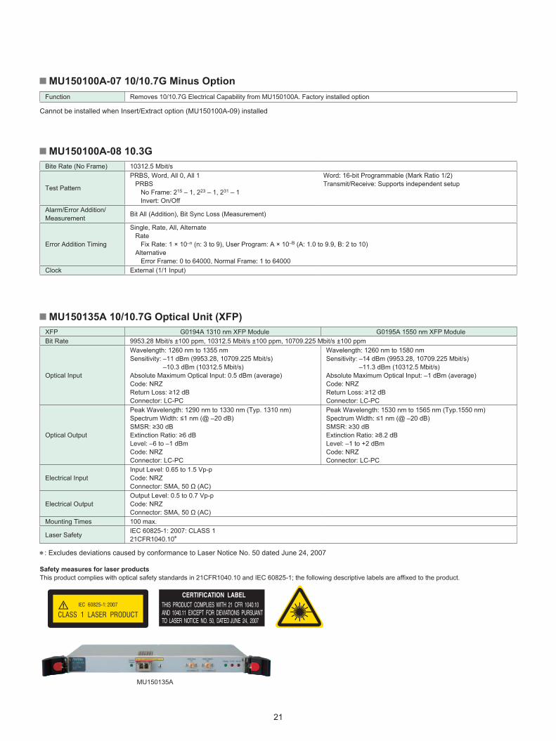
MU150135A 10/10.7G Optical Unit (XFP)XFP G0194A 1310 nm XFP Module G0195A 1550 nm XFP ModuleBit Rate 9953.28 Mbit/s ±100 ppm, 10312.5 Mbit/s ±100 ppm, 10709.225 Mbit/s ±100 ppm
Optical Input
Wavelength: 1260 nm to 1355 nmSensitivity: –11 dBm (9953.28, 10709.225 Mbit/s)
–10.3 dBm (10312.5 Mbit/s)Absolute Maximum Optical Input: 0.5 dBm (average)Code: NRZReturn Loss: ≥12 dBConnector: LC-PC
Wavelength: 1260 nm to 1580 nmSensitivity: –14 dBm (9953.28, 10709.225 Mbit/s)
–11.3 dBm (10312.5 Mbit/s)Absolute Maximum Optical Input: –1 dBm (average)Code: NRZReturn Loss: ≥12 dBConnector: LC-PC
Optical Output
Peak Wavelength: 1290 nm to 1330 nm (Typ. 1310 nm)Spectrum Width: ≤1 nm (@ –20 dB)SMSR: ≥30 dBExtinction Ratio: ≥6 dBLevel: –6 to –1 dBmCode: NRZConnector: LC-PC
Peak Wavelength: 1530 nm to 1565 nm (Typ.1550 nm)Spectrum Width: ≤1 nm (@ –20 dB)SMSR: ≥30 dBExtinction Ratio: ≥8.2 dBLevel: –1 to +2 dBmCode: NRZConnector: LC-PC
Electrical InputInput Level: 0.65 to 1.5 Vp-pCode: NRZConnector: SMA, 50 Ω (AC)
Electrical OutputOutput Level: 0.5 to 0.7 Vp-pCode: NRZConnector: SMA, 50 Ω (AC)
Mounting Times 100 max.
Laser Safety IEC 60825-1: 2007: CLASS 121CFR1040.10∗
∗: Excludes deviations caused by conformance to Laser Notice No. 50 dated June 24, 2007
Safety measures for laser productsThis product complies with optical safety standards in 21CFR1040.10 and IEC 60825-1; the following descriptive labels are affixed to the product.
MU150135A
22
Please specify the model/order number, name and quantity when ordering.The names listed in the chart below are Order Names. The actual name of the item may differ from the Order Name.
Ordering Information
Model/Order No. Name–Main Frame–
MP1595A 40G SDH/SONET Analyzer–Standard Accessories–
J0491 Sield Power Cord 2.6 m (13 A)∗1: 1 pcJ0670A Power Cord L Type (C7), 2.5 m∗1: 1 pcF0105 Fuse 10 A∗1: 2 pcsB0482 Front Cover (3/4MW5U)∗1: 1 pcJ1003S Semirigid Cable, 56.5 mm∗2, ∗3: 1 pcJ1003N Semirigid Cable, 136.6 mm∗2: 1 pcJ0635A Optical Fiber Cable
(SM, FC-SPC connector both ends), 1 m∗4: 1 pcJ0617B Replaceable Optical Connector (FC-PC)∗3, ∗4: 2 pcsJ1383A Semirigid Cable, 105.7 mm∗5: 1 pcJ1384A Semirigid Cable, 90.0 mm∗5: 1 pcJ0747C Fixed Optical Attenuator (15 dB, FC connector)∗3: 1 pc
–Units/Modules–MU150100A 10/10.7G Unit∗6
MU150135A 10/10.7G Optical Unit (XFP)∗7
MU150140A 40/43G UnitMU150141A 40G Optical UnitMU150141B 40/43G Optical UnitMU150147A 40/43G Jitter Unit∗8
MU150149A 40/43G Optical Unit (TX)∗8
–Software–MX159501A 40G SDH/SONET Analyzer Control SoftwareMX159508A Jitter/Wander Measurement Software∗9
–Option–MP1595A-01 RS-232CMP1595A-02 GPIBMP1595A-03 LANMP1595A-004 Clock Source Output for Jitter/Wander∗10
MP1595A-104 Clock Source Output for Jitter/Wander Retrofit∗10
MU150140A-05 OTU3MU150140A-06 ODTU23∗11
MU150140A-10 Frame Memory/Capture (40/43G)MU150141A-40 SC ConnectorMU150141B-40 SC ConnectorMU150147A-001 39.813 Gbit/s∗12
MU150147A-002 43.018 Gbit/s∗12
MU150147A-007 Fast Jitter Transfer MeasurementMU150147A-008 Demod Signal AnalysisMU150147A-009 Demod OutputMU150147A-010 Wander MeasurementMU150147A-011 Wander GenerationMU150147A-040 SC ConnectorMX159508A Jitter/Wander Measurement SoftwareMU150100A-01 Wavelength 1.31 μmMU150100A-02 Wavelength 1.55 μmMU150100A-03 Wavelength 1.31/1.55 μmMU150100A-04 Optical Output Power AdjustableMU150100A-05 OTU1/OTU2MU150100A-07 10/10.7G Minus Option∗13
MU150100A-08 10.3G∗14
MU150100A-09 Insert/Extract∗13
MU150100A-38 ST Connector∗15
MU150100A-39 DIN Connector∗15
MU150100A-40 SC Connector∗15
MU150100A-43 HMS-10/A Connector∗15
–Optional Accessories–B0483 Carrying CaseB0593A Blank PanelG0194A 1310 nm XFP Module∗16
G0195A 1550 nm XFP Module∗16
J0008 GPIB cable, 2 mJ0845 Balanced Cable (BANTAM 3P-BANTAM 3P), 6 ftJ0162A Balanced Cable (Siemens 3P-Siemens 3P), 1 mJ0162B Balanced Cable (Siemens 3P-Siemens 3P), 2 mJ0322B Coaxial Cable (11SMA SUCOFLEX104 11SMA), 1 mJ0617B Replaceable Optical Connector (FC-PC)J0635B Optical Fiber Cable (SM, FC-SPC connector both ends), 2 mJ0635C Optical Fiber Cable (SM, FC-SPC connector both ends), 3 mJ0660B Optical Fiber Cable (SM, SC-SC connector both ends), 2 m
Model/Order No. NameJ0747A Fixed Optical Attenuator (5 dB, FC connector)J0747B Fixed Optical Attenuator (10 dB, FC connector)J0747C Fixed Optical Attenuator (15 dB, FC connector)J0747D Fixed Optical Attenuator (20 dB, FC connector)J0775D Coaxial cable (BNC-P620 3C-2WS BNC-P620 75 Ω), 2 mJ0776D Coaxial cable (BNC-P-3W/3D-2W/BNC-P-3W, 50 Ω), 2 mJ0796A ST Connector (replaceable, with protective caps, 1 set)J0796B DIN Connector (replaceable, with protective caps, 1 set)J0796C SC Connector (replaceable, with protective caps, 1 set)J0796D HMS-10/A Connector (replaceable, with protective caps, 1 set)J0796E FC Connector (replaceable, with protective caps, 1 set)J1003S Semirigid Cable, 56.5 mmJ1003N Semirigid Cable, 136.6 mmJ1049A Fixed Optical Attenuator (5 dB, SC connector)J1139A Optical Fiber Cable (SM, FC-LC connector both ends), 1 mJ1271 Optical Fiber Cable (Duplex, SM, LC-LC connector), 2 mJ1272 Optical Fiber Cable (Duplex, SM, LC-SC connector), 2 mJ1327B Optical Fiber Cable (SM, LC-LC connector both ends), 2 mJ1344A Optical Fiber Cable (SM, LC-LC connector both ends), 1 mJ1139A Optical Fiber Cable (SM, LC-FC connector both ends), 1 mJ1376A Fixed Optical Attenuator (5 dB, LC connector)J1383A Semirigid Cable, 105.7 mmJ1384A Semirigid Cable, 90.0 mmZ0282 Ferrule Cleaner 1 CLETOP typeZ0283 Replacement Reels for Ferrule Cleaner 1 6/packZ0284 Adapter Cleaner 1 Stick type (200/set)Z0321A Keyboard (PS/2)Z0541A USB MouseZ0849A MD1230/MP1590 Family Manual CDZ0989A 1310 nm XFP Kit∗17
Z0990A 1550 nm XFP Kit∗18
W2869AE MP1595A Operation ManualW2937AE MX159501A Operation SDH Edition ManualW2938AE MX159501A Operation SONET Edition ManualW2939AE MP1595A Remote Control Operation ManualW2424AE MU150100A Specifications Operation ManualW2870AE MU150135A Specifications Operation ManualW2871AE MU150140A Specifications Operation ManualW2872AE MU150141A/B Specifications Operation Manual
∗1: Supplied with main frame∗2: Supplied with MU150140A∗3: Supplied with MU150100A∗4: Supplied with MU150141A or MU150141B∗5: Supplied with MU150135A∗6: One of MU150100A-01, 02, 03 required.∗7: Requires XFP module (sold separately).
In addition, operation with non-Anritsu modules not guaranteed.∗8: The MU150147A and MU150149A are not compliant with the CE
marking EMC (electromagnetic compatibility) regulations.∗9: Jitter and wander measurement requires MX159508A.∗10: The Jitter and wander measurement must need MP1595A-004/104.∗11: Requires separate MU150140-05 OTU3 option.∗12: MU150147A must need MU150147A-001 and MU150147A-002.
It does not operate at either one.∗13: MU150100A-07 factory installed only. MU150100A-07 and
MU150100A-09 cannot both be installed simultaneously.∗14: External clock source is required.∗15: Exchangeable.∗16: XFP modules sold as single units.
One can be mounted in MU150135A.∗17: Z0989A includes G0194A and J1344A.∗18: Z0990A includes G0195A, J1344A, and J1376A.
Maintenance ServiceName Model/Order No.
2 Years Extended Warranty Service Option-ES2103 Years Extended Warranty Service Option-ES3105 Years Extended Warranty Service Option-ES510
∗: These options extend the 1-year guarantee at purchase.

23
Note
• United StatesAnritsu Company1155 East Collins Blvd., Suite 100, Richardson, TX 75081, U.S.A.Toll Free: 1-800-267-4878Phone: +1-972-644-1777Fax: +1-972-671-1877
• CanadaAnritsu Electronics Ltd.700 Silver Seven Road, Suite 120, Kanata, Ontario K2V 1C3, CanadaPhone: +1-613-591-2003 Fax: +1-613-591-1006
• Brazil Anritsu Eletrônica Ltda.Praça Amadeu Amaral, 27 - 1 Andar01327-010 - Bela Vista - São Paulo - SP - BrazilPhone: +55-11-3283-2511Fax: +55-11-3288-6940
• MexicoAnritsu Company, S.A. de C.V.Av. Ejército Nacional No. 579 Piso 9, Col. Granada11520 México, D.F., MéxicoPhone: +52-55-1101-2370Fax: +52-55-5254-3147
• United KingdomAnritsu EMEA Ltd.200 Capability Green, Luton, Bedfordshire, LU1 3LU, U.K.Phone: +44-1582-433200 Fax: +44-1582-731303
• FranceAnritsu S.A.12 avenue du Québec, Bâtiment Iris 1- Silic 612,91140 VILLEBON SUR YVETTE, FrancePhone: +33-1-60-92-15-50Fax: +33-1-64-46-10-65
• GermanyAnritsu GmbHNemetschek Haus, Konrad-Zuse-Platz 1 81829 München, Germany Phone: +49-89-442308-0 Fax: +49-89-442308-55
• ItalyAnritsu S.r.l.Via Elio Vittorini 129, 00144 Roma, ItalyPhone: +39-6-509-9711 Fax: +39-6-502-2425
• SwedenAnritsu ABBorgarfjordsgatan 13A, 164 40 KISTA, SwedenPhone: +46-8-534-707-00 Fax: +46-8-534-707-30
• FinlandAnritsu ABTeknobulevardi 3-5, FI-01530 VANTAA, FinlandPhone: +358-20-741-8100Fax: +358-20-741-8111
• DenmarkAnritsu A/S (Service Assurance)Anritsu AB (Test & Measurement)Kay Fiskers Plads 9, 2300 Copenhagen S, DenmarkPhone: +45-7211-2200Fax: +45-7211-2210
• RussiaAnritsu EMEA Ltd. Representation Office in RussiaTverskaya str. 16/2, bld. 1, 7th floor.Russia, 125009, MoscowPhone: +7-495-363-1694Fax: +7-495-935-8962
• United Arab EmiratesAnritsu EMEA Ltd.Dubai Liaison OfficeP O Box 500413 - Dubai Internet CityAl Thuraya Building, Tower 1, Suit 701, 7th FloorDubai, United Arab EmiratesPhone: +971-4-3670352Fax: +971-4-3688460
• SingaporeAnritsu Pte. Ltd.60 Alexandra Terrace, #02-08, The Comtech (Lobby A)Singapore 118502Phone: +65-6282-2400Fax: +65-6282-2533
• IndiaAnritsu Pte. Ltd. India Branch Office3rd Floor, Shri Lakshminarayan Niwas, #2726, 80 ft Road, HAL 3rd Stage, Bangalore - 560 075, IndiaPhone: +91-80-4058-1300Fax: +91-80-4058-1301
• P.R. China (Shanghai)Anritsu (China) Co., Ltd.Room 1715, Tower A CITY CENTER of Shanghai, No.100 Zunyi Road Chang Ning District, Shanghai 200051, P.R. ChinaPhone: +86-21-6237-0898Fax: +86-21-6237-0899
• P.R. China (Hong Kong)Anritsu Company Ltd.Units 4 & 5, 28th Floor, Greenfield Tower, Concordia Plaza, No. 1 Science Museum Road, Tsim Sha Tsui East, Kowloon, Hong Kong, P.R. ChinaPhone: +852-2301-4980Fax: +852-2301-3545
• JapanAnritsu Corporation8-5, Tamura-cho, Atsugi-shi, Kanagawa, 243-0016 JapanPhone: +81-46-296-1221Fax: +81-46-296-1238
• KoreaAnritsu Corporation, Ltd.502, 5FL H-Square N B/D, 681Sampyeong-dong, Bundang-gu, Seongnam-si, Gyeonggi-do, 463-400 KoreaPhone: +82-31-696-7750Fax: +82-31-696-7751
• AustraliaAnritsu Pty. Ltd.Unit 21/270 Ferntree Gully Road, Notting Hill, Victoria 3168, AustraliaPhone: +61-3-9558-8177Fax: +61-3-9558-8255
• TaiwanAnritsu Company Inc.7F, No. 316, Sec. 1, NeiHu Rd., Taipei 114, TaiwanPhone: +886-2-8751-1816Fax: +886-2-8751-1817
Specifications are subject to change without notice.
1110
Printed on Recycled Paper
Please Contact:
Catalog No. MP1595A-E-A-1-(5.00) Printed in Japan 26/OCT/2011 ddcw/CDT