prof. ali m. niknejad berkeley wireless research center...
TRANSCRIPT

UNIVERSITY OF CALIFORNIA, BERKELEY Prof. Niknejad: Multiband and Multimode VCO Design
Multi-Mode and Wideband VCO Design
Prof. Ali M. NiknejadBerkeley Wireless Research CenterUniversity of California, Berkeley

UNIVERSITY OF CALIFORNIA, BERKELEY Prof. Niknejad: Multiband and Multimode VCO Design
Outline
● Introduction● Oscillator Start-up ● Basic Oscillator Topologies● Simple Theory of Phase Noise● Varactors (MOS, PN Junction, Switch)● Switching LC Resonators● Design Example: Wideband CMOS VCO

UNIVERSITY OF CALIFORNIA, BERKELEY Prof. Niknejad: Multiband and Multimode VCO Design
Introduction
● Multi-band synthesizer requires VCOs at multiple frequencies● Simple solution: Build multiple VCOs for each band and switch between
bands ● Multiple VCOs can be physical large due to passives● Good frequency planning can re-use a single VCO by changing PLL divide
ratios● To accommodate various standards and to simplify frequency planning, a
wide tuning range is desirable ● To keep noise low in PLL, the gain of the VCO should be small
UNIVERSITY OF CALIFORNIA, BERKELEY Prof. Niknejad: Multiband and Multimode VCO Design
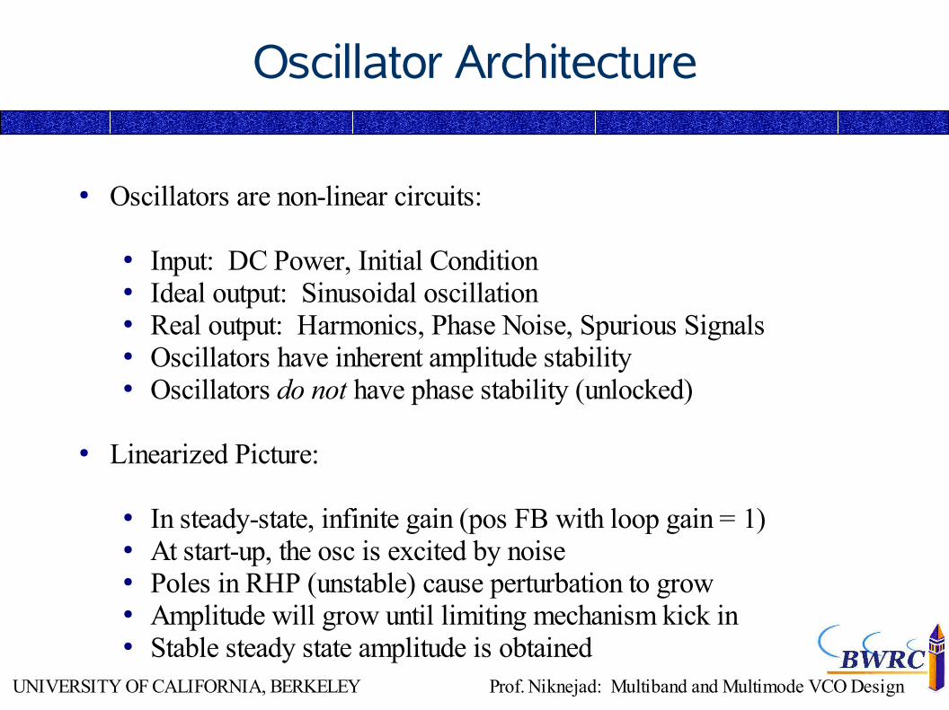
Oscillator Architecture
● Oscillators are non-linear circuits:
● Input: DC Power, Initial Condition● Ideal output: Sinusoidal oscillation ● Real output: Harmonics, Phase Noise, Spurious Signals● Oscillators have inherent amplitude stability ● Oscillators do not have phase stability (unlocked)
● Linearized Picture:
● In steady-state, infinite gain (pos FB with loop gain = 1)● At start-up, the osc is excited by noise ● Poles in RHP (unstable) cause perturbation to grow● Amplitude will grow until limiting mechanism kick in ● Stable steady state amplitude is obtained

UNIVERSITY OF CALIFORNIA, BERKELEY Prof. Niknejad: Multiband and Multimode VCO Design
Oscillator Start-Up: Feedback Perspective
● Positive feedback places poles at start-up in RHP● The loop gain determined by g
m, feedback factor, tank impedance
● Large signal Gm has limiting characteristics
● Amplitude grows until loop gain is unity (infinite gain)● In steady-state, poles on jw axis● Any amplitude perturbation is rejected
Al ,0=gmR
n1
Al=GmR
n=1

UNIVERSITY OF CALIFORNIA, BERKELEY Prof. Niknejad: Multiband and Multimode VCO Design
Oscillator Start-Up: Negative Resistance
● An oscillator is composed of a lossy tank and a regeneration circuit that has net negative resistance
● At start-up the negative resistance is larger than positive resistance for start-up (RHP pole)
● Steady-state negative resistance cancels the positive resistance of tank (zero net loss)
● Amplitude determined by large signal limiting of resistance● Equivalent to FB picture for 2-port devices● Possible to use 1-port “active” devices (Gunn Diodes)

UNIVERSITY OF CALIFORNIA, BERKELEY Prof. Niknejad: Multiband and Multimode VCO Design
Oscillator Topologies
● Ring Oscillators● Tuned Ring Oscillators● Distributed Oscillators● LC Tank positive feedback circuits:
● Transformer feedback● Capacitive transformer feedback● Tapped inductor feedback● LC feedback
● Single-ended versus differential● Grounding options● FET versus BJT (1/f noise, amplitude of osc)

UNIVERSITY OF CALIFORNIA, BERKELEY Prof. Niknejad: Multiband and Multimode VCO Design
Oscillator Topologies (2)
● Single ended● Colpitts Oscillator has capacitive feedback
● Common base/gate: capacitor feedback has no phase inversion ● Hartley and Pierce (dual of Colpitts)● Clap, Armstrong, ...

UNIVERSITY OF CALIFORNIA, BERKELEY Prof. Niknejad: Multiband and Multimode VCO Design
Oscillator Topologies (3)
● Differential● Cross coupled diff pair (MOS can be better than BJT)● Colpitts (capacitor feedback for higher swing in BJT)● Colpitts with built-in buffer (take output at collector)
● PMOS versus NMOS (lower 1/f noise since PMOS device is not a surface device)
● Advantage is disappearing in ultra-short channel devices (0.13mm)

UNIVERSITY OF CALIFORNIA, BERKELEY Prof. Niknejad: Multiband and Multimode VCO Design
Oscillator Topologies (4)
● Current source inject 1/f noise into “mixer”● DC and all even harmonics can form mixing products at fund. ● Use a large PMOS device or even a resistor● Use filter at current source to suppress noise● Double-differential ... (PMOS and NMOS cross-coupled pair)

UNIVERSITY OF CALIFORNIA, BERKELEY Prof. Niknejad: Multiband and Multimode VCO Design
Resonators Quality Factor
● The quality factor for a resonant system is defined as the product of the resonant frequency times the energy stored per cycle over the power loss.
● From Poynting's Theorem we can find the power in the electromagnetic field in a volume of space
● From circuit theory
Q= Av. Energy StoredPower Loss
=U mU e
P l
P= P0powercrossing surface
P lpower loss
2 jU m−U epower stored
Z i=VI=VI∣I∣2=2P
∣I∣2R=
PoP l
12∣I∣2
X=4U m−U e
12∣I∣2

UNIVERSITY OF CALIFORNIA, BERKELEY Prof. Niknejad: Multiband and Multimode VCO Design
Simple Phase Noise Theory
● Since any real system has noise, the “input” to an oscillator is not zero but finite (very small)
● The noise spectrum is shaped by tuned positive feedback amplifier● Signals near tank resonance see very large gain due to positive feedback
with loop gain < 1● The actual loop gain never reaches unity but is very close to one● Integrate spectral power density to find loop gain

UNIVERSITY OF CALIFORNIA, BERKELEY Prof. Niknejad: Multiband and Multimode VCO Design
Phase Noise Theory (2)
● Compute transfer function for input referred voltage noise ● Integrate expression to obtain total oscillator power
● Loop gain is not unity (but nearly so):
v2, rms2 =
vn2 Al
2n2
1−Al240
2
Q2
∫−∞∞ d
1a2=/a
Posc=vn
2
Rn2
21RC
Al2
1−Al
1−Al=
vn2
RPosc
2
1RC

UNIVERSITY OF CALIFORNIA, BERKELEY Prof. Niknejad: Multiband and Multimode VCO Design
Phase Noise Theory (3)
● This simple theory does not account for non-linear and noise mixing effects● 1/f noise from current source is mixed to RF (even harmonics)● Gain compression (use steady-state gm)● Oscillator can be approximated as a cyclostationary system (time of
noise injection is important [Kaertner] [ Hajimiri])● But it's a good first-order theory (Leeson equations) that highlight the
importance of tank Q● Oscillator Figures of merit can be defined accordingly● More Discussion of this approach can be found:
Phase noise in LC oscillators Kouznetsov, K.A.; Meyer, R.G.; Solid-State Circuits, IEEE Journal of , Volume: 35 Issue: 8 , Aug 2000 Page(s): 1244 -1248

UNIVERSITY OF CALIFORNIA, BERKELEY Prof. Niknejad: Multiband and Multimode VCO Design
Multi-Mode Resonators
● On-chip spiral inductor have multiple resonance frequencies (shorted T-line resonates at odd multiples of /4)
● Why not use second harmonic for second band?● Transformer has two fundamental resonant modes (in phase and
differential):
● High frequency mode has lower Q (energy storage)
U m=12L1 I 1
2L2 I 22±M I 2 I 2
Leff =L1L2±2M

UNIVERSITY OF CALIFORNIA, BERKELEY Prof. Niknejad: Multiband and Multimode VCO Design
Wideband VCOs
● Challenge of realizing wide tuning range ● Loop gain must be high enough over entire range● Must design for worse case (high current consumption)● Amplitude of oscillation a function of frequency
● Amplitude control loop (ACL) can provide just enough feedback to keep loop gain = 1 over entire range
● ACL subject to noise issues
V osc≈2 I bias RT
RT≈Q L∝2
V osc ∝a

UNIVERSITY OF CALIFORNIA, BERKELEY Prof. Niknejad: Multiband and Multimode VCO Design
Varactors for RF Applications
● Common technique for frequency variation is to vary the cap ● PN junction diodes are ubiquitous, MOS capacitors good alternative● MOS capacitors have larger tuning range (2:1) but also higher “gain”
(achieve tuning range over a narrow voltage swing)● Many options for MOS varactors:
● n-type or p-type, triple well for isolation● inversion mode versus accumulation mode● body bias (inversion only or accumulation only)
● Noise on control line and substrate reception an important consideration

UNIVERSITY OF CALIFORNIA, BERKELEY Prof. Niknejad: Multiband and Multimode VCO Design
Variable Inductors?
● Transformer technique: sense primary current and amplify secondary● Active circuit sets linearity and noise limits ● Active circuit must handle resonant current in secondary!● Resonant circuit current is Q times larger than oscillator current● Phase delay in secondary current can create loss
vs= j L1 i1 jM i2= jL1K M i1
Variable current gain
Leff =L1K M

UNIVERSITY OF CALIFORNIA, BERKELEY Prof. Niknejad: Multiband and Multimode VCO Design
Varactors: PN Junction Diodes
● Forward bias issues limits swing● Biasing and noise requires AC isolation and filtering● High tuning voltage for wideband operation● Need extra process steps to optimize performance (high doping to
minimize series resistance due to substrate loss)

UNIVERSITY OF CALIFORNIA, BERKELEY Prof. Niknejad: Multiband and Multimode VCO Design
Varactors: MOS Capacitors
● Accumulation or inversion Mode ● Accumulation mode preferred (higher electron mobility)● Tuning range is very large due to fast charge build-up● CV equation follows from solution of Poisson's equation:
Cg
Cox=
W0 2Vt
e−Vgb−Vfb
2Vt
1W0 2Vt
e−Vgb−Vfb
2Vt (W0 is product-log function)

UNIVERSITY OF CALIFORNIA, BERKELEY Prof. Niknejad: Multiband and Multimode VCO Design
Varactors: Switched-Capacitors
● MOS device is a pretty good switch (parasitic on resistance and off capacitance)
● PN Junction can also be switched between “low” and “high” cap ● Why not switched inductor? Low inductor Q prevents use unless switch
has very low on-resistance

UNIVERSITY OF CALIFORNIA, BERKELEY Prof. Niknejad: Multiband and Multimode VCO Design
MOS Switched-Capacitor Topologies
● Binary weighted array of capacitors and switches● Can select discrete sub-bands and tune with variable capacitor● Band overlap by some safety margin● Tuning range limited by parasitic off capacitance● Quality factor limited by on-resistance● Device size chosen large enough such that the overall tank Q dominated by
inductor ● Differential topology also possible

UNIVERSITY OF CALIFORNIA, BERKELEY Prof. Niknejad: Multiband and Multimode VCO Design
Switched-Capacitor Design Equations
● Size does matter:● Series loss goes down with W● Parasitic capacitance goes up with W● Tuning Range and Q tradeoff
● Max/min frequency of oscillation
● Frequency overlap inequality:
max :1
0,max2 L
=C ,min2n−1 1
Cdd
1Ca−1
C p
min :1
0,min2 L
=C ,max2n−1CaC p
C ,max−C ,minCa− 1Cdd
1Ca−1
UNIVERSITY OF CALIFORNIA, BERKELEY Prof. Niknejad: Multiband and Multimode VCO Design
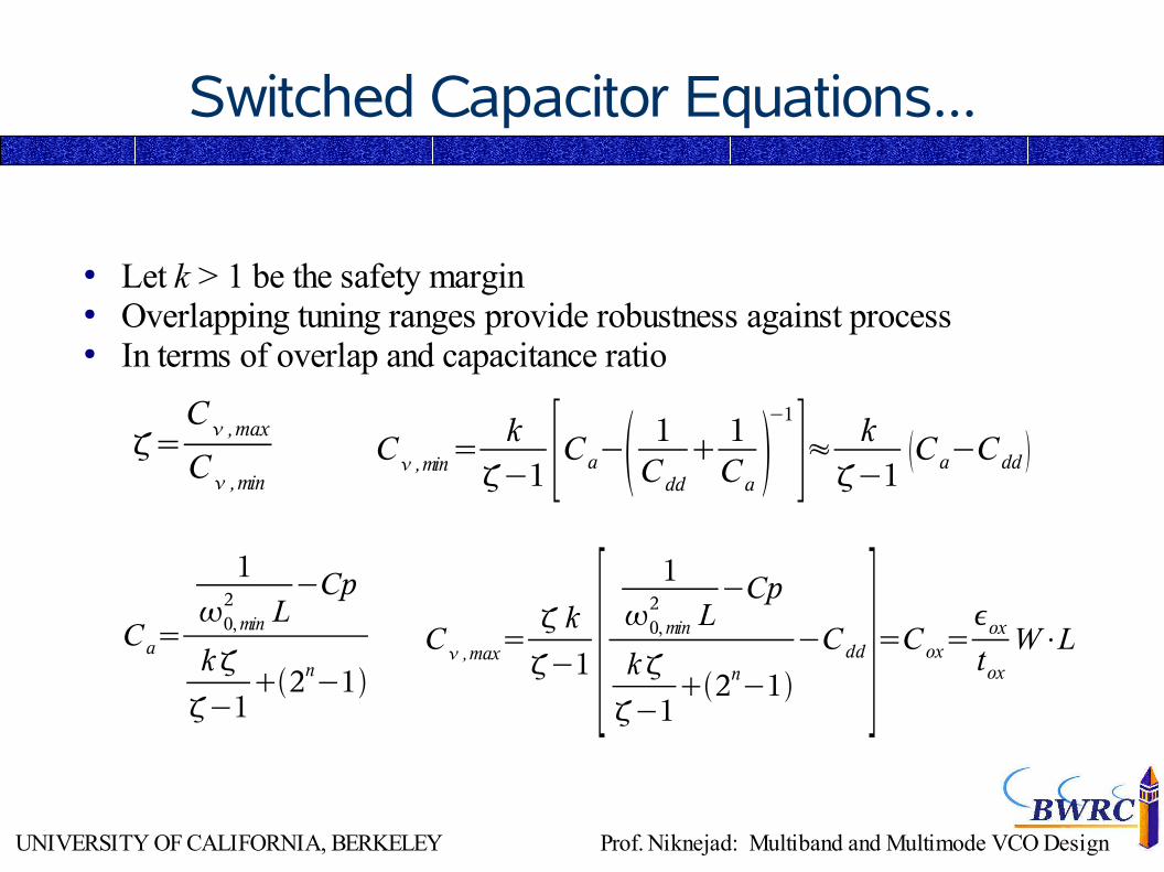
Switched Capacitor Equations...
● Let k > 1 be the safety margin ● Overlapping tuning ranges provide robustness against process ● In terms of overlap and capacitance ratio
=C ,maxC ,min
C ,min=k−1 [Ca− 1
Cdd
1Ca−1]≈ k
−1Ca−Cdd
Ca=
1
0,min2 L
−Cp
k−1
2n−1C ,max=
k−1 [ 1
0,min2 L
−Cp
k−1
2n−1−C dd ]=Cox=
oxtox
W⋅L

UNIVERSITY OF CALIFORNIA, BERKELEY Prof. Niknejad: Multiband and Multimode VCO Design
Switched Capacitor Q Factor
● The on-resistance of a FET switch in triode region:
● The channel resistance of a MOS accumulation mode varactor (Factor of 12 due to distributed effects):
● Switch-capacitor Quality Factor (independent of n)
Ron=LW
1nCox V gs−V t
Rc=LW
112 pCox V gs−V t
Qc=0 1
0RonCa21 Ron2n−1
2n−1Ca
Qc≃1
0RonCa

UNIVERSITY OF CALIFORNIA, BERKELEY Prof. Niknejad: Multiband and Multimode VCO Design
Example: CMOS Wideband VCO
4W/L
4C
2W/L
2C
1W/L
C
B2 B1 B0
Vtune
Vo-
LB
M3
M1 M2
M4
IB
Vo+ Vo
-
Vtune
● All PMOS to reduce 1/f noise● Only 2 gain devices to minimize
cap loading.● Large area tail device since main
1/f contributor● P+/Nwell varactors● Very compact integrated varactor
bias chokes ● LB = 100nH at only 100μm/side!!
Ref: Axel Berny et al. (to appear at CICC '03)

UNIVERSITY OF CALIFORNIA, BERKELEY Prof. Niknejad: Multiband and Multimode VCO Design
CMOS Wideband VCO Die Photo
● Dimensions:
1600 x 1500 mm2
● Technology: IBM 0.25mm RF CMOS process
● 5 Al metal layers● To appear at CICC '03
VCO core
chokes
output buffer
P+/nwellvaractor
Cap array
Tail device

UNIVERSITY OF CALIFORNIA, BERKELEY Prof. Niknejad: Multiband and Multimode VCO Design
Measured Performance
● Measured tuning range:1.06-1.41 GHz or 28.3%● Simulated tuning range: 1.06-1.46 GHz or 31.7%
1.05
1.10
1.15
1.20
1.25
1.30
1.35
1.40
1.45
0.0 0.5 1.0 1.5 2.0 2.5 3.0
000
001
010
011
100
101
110
111
Tuning Voltage (V)
Fre
que
ncy
of O
scil
lati
on (
GH
z)

UNIVERSITY OF CALIFORNIA, BERKELEY Prof. Niknejad: Multiband and Multimode VCO Design
Measured and Simulated Phase Noise
VDD = 2 V, Vtune = 0|1.5 V, Icore = 3.6 mA
-135
-130
-125
-120
-115
-110
-105
1.10 1.15 1.20 1.25 1.30 1.35 1.40Frequency of Oscillation (GHz)
Pha
se N
oise
(dB
c/H
z) L(f=100 kHz)
L(f=1 MHz)
104
105
106
107
108
-160
-150
-140
-130
-120
-110
-100
-90
-80
L (d
Bc/H
z)
Frequency Offset (Hz)
Vtune=1.5V, B2B1B0=011
Vtune=0.0V, B2B1B0=000

UNIVERSITY OF CALIFORNIA, BERKELEY Prof. Niknejad: Multiband and Multimode VCO Design
Performance Summary
Technology
Supply Voltage 2 V
Current (VCO Core) 3.6 mA
Tuning Range 28.00%
< 75 Mhz/V
-111 dBc/Hz
-127 dBc/Hz
-131 dBc/Hz
.25 μm CMOS
Tuning Sensitivity (KVCO)
Phase Noise (f = 1.244 Ghz, Δf = 100 kHz)
Phase Noise (f = 1.244 Ghz, Δf = 600 kHz)
Phase Noise (f = 1.244 Ghz, Δf = 1 Mhz)

UNIVERSITY OF CALIFORNIA, BERKELEY Prof. Niknejad: Multiband and Multimode VCO Design
Summary
● VCO design is a careful tradeoff between power, noise, and passive element design and optimization
● Multi-band voltage controlled oscillators can be realized easily with a switched capacitor array
● Quality factor of switched capacitor array only a function of technology (low on-resistance for fixed parasitics)
● MOS varactors offer wide tuning range over small voltage swings
● Switch capacitor arrays decouple VCO gain K from achievable tuning range