programmable pll (si570) local oscillator for hf · pdf filetitle revision aaøzz-si570...
TRANSCRIPT

Title Revision
AAØZZ-Si570 Prog-PLL 110718
Programmable PLL (Si570) Local Oscillator for HF Receivers, Transmitters, Transceivers
TABLE OF CONTENTS
1. INTRODUCTION ................................................................................................................................. 3
2. Si570 Operation.................................................................................................................................. 3
2.1. Si570 Functional Description ........................................................................................................ 4
2.2. Si570 Output Frequency Generation ............................................................................................ 4
2.3. Si570 Freeze DCO ....................................................................................................................... 5
2.4. Freeze M ...................................................................................................................................... 7
2.5. Si570 RF Output .......................................................................................................................... 7
2.6. Si570 RF Output Impedance ........................................................................................................ 8
2.7. I2C Communications .................................................................................................................... 9
2.7.1. Level Shifter ................................................................................................................................. 9
3. Si570 Daughtercard ......................................................................................................................... 10
3.1. Daughtercard with PIC-EL .......................................................................................................... 11
3.2. Daughtercard with Control Board ............................................................................................... 12
3.3. Daughtercard and Control Board Current Draw .......................................................................... 13
4. PEgen570 Software Application ..................................................................................................... 13

2
4.1. 16F88 PIC .................................................................................................................................. 13
4.2. I2C Communications .................................................................................................................. 13
4.3. Frequency Selection Method ...................................................................................................... 14
4.4. DCO Freeze Handling ................................................................................................................ 15
4.5. Major Subroutines of PEgen570 ................................................................................................. 15
4.5.1. Frequency Selection - CalcRFREQ( ) ......................................................................................... 15
4.5.2. Calibration - CalcHSN1Entry( ) .................................................................................................. 17
4.6. Si570 Bands ............................................................................................................................... 19
4.6.1. Band Tables ............................................................................................................................... 20
4.7. User Interface............................................................................................................................. 21
4.8. Menu .......................................................................................................................................... 21
4.8.1. Sideband Selection .................................................................................................................... 22
4.8.2. CW Sidetone During Receive ..................................................................................................... 22
4.8.3. Frequency Division for LCD Display ........................................................................................... 22
4.8.4. FSK Frequency Shift .................................................................................................................. 22
4.9. LCD Display ............................................................................................................................... 23
4.10. Debug Mode .............................................................................................................................. 23
4.11. Ideas for Future Modification ...................................................................................................... 23
5. Example Receivers and Transmitters Using the Si570 Programmable PLL ................................ 24
5.1. Block Diagram – CW or SSB Receiver ....................................................................................... 24
5.2. Schematic - Rx Using the Si570 P-PLL and a PC for Audio Processing ..................................... 24
5.3. Schematic - KK7B MicroR2 Receiver Using the Si570 P-PLL .................................................... 25
5.4. Block Diagram - CW Transmitter ................................................................................................ 26
5.5. Schematic - 40-Meter CW Transmitter Using the Si570 P-PLL ................................................... 26
5.6. Block Diagram - 40-Meter SSB Transmitter Using the Si570 P-PLL ........................................... 26
6. Schematic - AA0ZZ Si570 Daughtercard ........................................................................................ 28
7. Schematic - AA0ZZ Si570 Control Board ....................................................................................... 29
8. Conclusion ....................................................................................................................................... 29

3
1. INTRODUCTION
A new product has recently been developed by Silicon Labs, the Si570 DSPLL® programmable frequency synthesizer, and it has great potential for use in many amateur radio applications. Here we will explore some possible uses. Phase lock loop technology has been in use for many years, but the ability to use variable software-supplied loop parameters in PLL technology to directly generate square waves with frequency resolutions of 1 Hz or less is now possible. The Si570 immediately puts the new technology into the sphere of uses that has been recently been dominated by Direct Digital Synthesis (DDS) products.
This AAØZZ Si570 Daughtercard uses the Silicon Labs Si570 (CMOS version) and, when controlled by a microcontroller, can generate RF signals in the continuous range of 10 to 157 MHz. (Other versions of the Si570 can go up to 1.4 GHz.) When the Daughtercard is incorporated into a control board, the Si570 Daughtercard can easily be used as the local oscillator of an amateur radio transceiver. Since many amateurs use divide-by-four mechanisms in Quadrature Sampling Detectors (QSD) – i.e, “Tayloe” mixers - for their receivers and also in Quadrature Sampling Exciters (QSE) for their transmitters (1), this Si570 Daughtercard can provide the local oscillator signal for these receivers and transmitters on the 80 through 10 meter amateur bands.
2. Si570 Operation
Figure 2-1 shows a block diagram of the Si570.
Figure 2-1 Si570 Block Diagram
The Si570 offers some significant advantages over the DDS parts that have been used by amateurs in applications in the past years. Two advantages are greatly reduced power consumption and the relatively clean output without DDS byproducts (spurs). The Si570 uses a combination of DSP processing and a PLL topology with frequency selection parameters set by the user via an I2C serial communications link to generate the desired output frequency.
Silicon Labs offers several versions of the Si570 with different output options and frequency limits. The Si570 version used in the AAØZZ Si570 Daughtercard is a CMOS part with a 10.0 MHz default frequency and a 160 MHz maximum frequency. The internal crystal of the Si570

4
runs at a nominal 114.285 MHz. However, the crystal in any individual part will not oscillate at exactly this frequency. Since the crystal frequency is used in the frequency generation calculations for the Si570 input parameter words, any deviation from nominal means that the Si570 generated frequency will not be accurate. Fortunately, Silicon Labs calibrates each individual part in the factory and saves the calibrated parameters in its nonvolatile memory to cause it to start up at the default frequency (in this case, 10.0 MHz). The software can retrieve these parameters from the nonvolatile memory and thus calculate the calibrated crystal frequency. This calibrated crystal frequency can then be used in subsequent calculations and the results will much more accurate than they would be if the nominal crystal frequency was used for the calculations.
2.1. Si570 Functional Description
The spec sheet of the Si570 is a real challenge to interpret. The description given here will not substitute for a thorough reading of the spec sheet but it will get you started.
Command data bytes are sent from the controller to the Si570 registers by way of the standard I2C serial communications protocol. (See Section 2.7 for details on I2C operation.) The basic control registers are shown in Figure 2-2.
7 6 5 4 3 2 1 0
Si Reg 7 HS_DIV_Index [2:0] (N1-1) [6:2]
Si Reg 8 (N1-1) [1:0] RFREQ(integer) [37:32]
Si Reg 9 RFREQ(integer) [31:28] RFREQ(fractional) [27:24]
Si Reg 10 RFREQ(fractional) [23:16]
Si Reg 11 RFREQ(fractional) [15:8]
Si Reg 12 RFREQ(fractional) [7:0]
Si Reg
135 RST_REG
New
Freq
Freeze
M RECALL
Si Reg
137
Freeze
DCO
Figure 2-2 Si570 Control Registers
2.2. Si570 Output Frequency Generation
The Si570 has a digitally-controlled oscillator (DCO), driven by a fixed-frequency crystal and PLL loop-control parameters. There are three frequency selection parameters that the software must set up for the Si570 to generate the desired output frequency. The basic frequency generation formula is:
Fout = (Fxtal * RFREQ) / (HS_DIV * N1)
where:
1) Fxtal is the fixed crystal frequency (114.285 MHz nominal) 2) RFREQ is a 38-bit variable consisting of a 10-bit integer and a 28-bit fraction 3) HS_DIV can be 4, 5, 6, 7, 9 or 11 4) N1 can be 1 or any even integer between (and including) 2 and 128
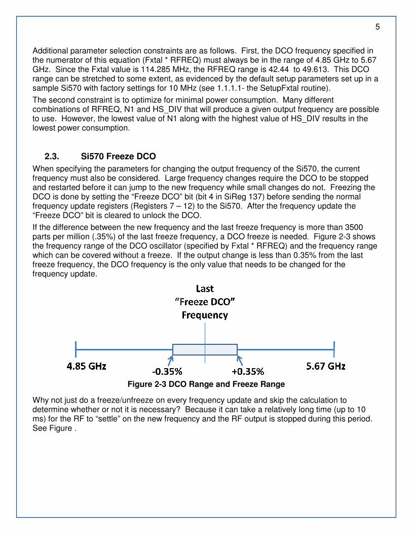
Additional parameter selection constraints are as follows. First, the DCO frequency specified in the numerator of this equation (Fxtal * RFREQ) must alwayGHz. Since the Fxtal value is 114.285 MHz, the RFREQ range is 42.44 to 49.613. This DCO range can be stretched to some extent, as evidenced by the default setup parameters set up in a sample Si570 with factory settings for 10 MHz (see
The second constraint is to optimize for minimal power consumption. Many different combinations of RFREQ, N1 and HS_DIV that will produce a given output frequency are possible to use. However, the lowest value of N1 lowest power consumption.
2.3. Si570 Freeze DCO
When specifying the parameters for changing thefrequency must also be considered. Large frequency changes require the DCO to be stopped and restarted before it can jump to the new frequency while small changes do not. Freezing the DCO is done by setting the “Freeze DCO” bit (bit 4 in SiReg 137) before sending the normal frequency update registers (Registers 7 “Freeze DCO” bit is cleared to unlock the DCO.
If the difference between the new frequency and theparts per million (.35%) of the last freeze frequency, a DCO freeze is needed. the frequency range of the DCO oscillator (specified by Fxtal * RFREQ) and the frequency range which can be covered without a freeze. If the output change is less than 0.35% from the last freeze frequency, the DCO frequency is the only value that needs to be changed for the frequency update.
Figure
Why not just do a freeze/unfreeze on evdetermine whether or not it is necessary? Because it can take a relatively long time (up to 10 ms) for the RF to “settle” on the new frequency and the RF output is stopped during this period. See Figure .
Additional parameter selection constraints are as follows. First, the DCO frequency specified in the numerator of this equation (Fxtal * RFREQ) must always be in the range of 4.85 GHz to 5.67 GHz. Since the Fxtal value is 114.285 MHz, the RFREQ range is 42.44 to 49.613. This DCO range can be stretched to some extent, as evidenced by the default setup parameters set up in a
ngs for 10 MHz (see 1.1.1.1- the SetupFxtal routine).
The second constraint is to optimize for minimal power consumption. Many different and HS_DIV that will produce a given output frequency are possible
he lowest value of N1 along with the highest value of HS_DIV results in the
Si570 Freeze DCO
When specifying the parameters for changing the output frequency of the Si570, the current frequency must also be considered. Large frequency changes require the DCO to be stopped and restarted before it can jump to the new frequency while small changes do not. Freezing the
“Freeze DCO” bit (bit 4 in SiReg 137) before sending the normal frequency update registers (Registers 7 – 12) to the Si570. After the frequency update the “Freeze DCO” bit is cleared to unlock the DCO.
If the difference between the new frequency and the last freeze frequency is more than 3500 parts per million (.35%) of the last freeze frequency, a DCO freeze is needed. the frequency range of the DCO oscillator (specified by Fxtal * RFREQ) and the frequency range
thout a freeze. If the output change is less than 0.35% from the last freeze frequency, the DCO frequency is the only value that needs to be changed for the
2-3 DCO Range and Freeze Range
Why not just do a freeze/unfreeze on every frequency update and skip the calculation to determine whether or not it is necessary? Because it can take a relatively long time (up to 10 ms) for the RF to “settle” on the new frequency and the RF output is stopped during this period.
5
Additional parameter selection constraints are as follows. First, the DCO frequency specified in s be in the range of 4.85 GHz to 5.67
GHz. Since the Fxtal value is 114.285 MHz, the RFREQ range is 42.44 to 49.613. This DCO range can be stretched to some extent, as evidenced by the default setup parameters set up in a
the SetupFxtal routine).
The second constraint is to optimize for minimal power consumption. Many different and HS_DIV that will produce a given output frequency are possible
the highest value of HS_DIV results in the
output frequency of the Si570, the current frequency must also be considered. Large frequency changes require the DCO to be stopped and restarted before it can jump to the new frequency while small changes do not. Freezing the
“Freeze DCO” bit (bit 4 in SiReg 137) before sending the normal 12) to the Si570. After the frequency update the
last freeze frequency is more than 3500 parts per million (.35%) of the last freeze frequency, a DCO freeze is needed. Figure 2-3 shows the frequency range of the DCO oscillator (specified by Fxtal * RFREQ) and the frequency range
thout a freeze. If the output change is less than 0.35% from the last freeze frequency, the DCO frequency is the only value that needs to be changed for the
ery frequency update and skip the calculation to determine whether or not it is necessary? Because it can take a relatively long time (up to 10 ms) for the RF to “settle” on the new frequency and the RF output is stopped during this period.

6
Figure 2-4 RF Dropout Following DCO Freeze
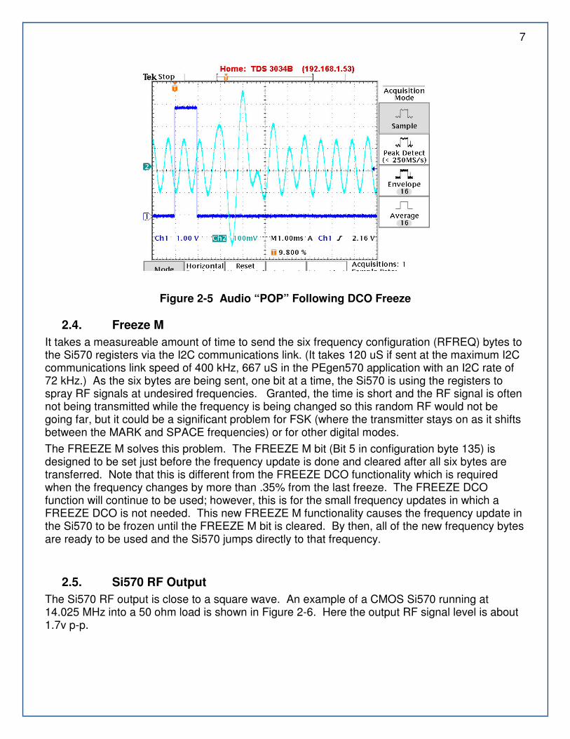
In this example, trace 1 is high during the freeze-update-unfreeze sequence (980 uS) and trace 4 shows the RF dropout (220 uS). The RF dropout which occurs when the SI570 is stopped and restarted at the new frequency after a DCO freeze causes an audible pop in a receiver. See Figure 2-5 for an oscilloscope screen shot of the audio pop. Channel 1 (dark blue) is high during the DCO freeze and Channel 2 (light blue) is the audio. Small frequency changes without a DCO freeze do not cause the pop sound.
7
Figure 2-5 Audio “POP” Following DCO Freeze
2.4. Freeze M
It takes a measureable amount of time to send the six frequency configuration (RFREQ) bytes to the Si570 registers via the I2C communications link. (It takes 120 uS if sent at the maximum I2C communications link speed of 400 kHz, 667 uS in the PEgen570 application with an I2C rate of 72 kHz.) As the six bytes are being sent, one bit at a time, the Si570 is using the registers to spray RF signals at undesired frequencies. Granted, the time is short and the RF signal is often not being transmitted while the frequency is being changed so this random RF would not be going far, but it could be a significant problem for FSK (where the transmitter stays on as it shifts between the MARK and SPACE frequencies) or for other digital modes.
The FREEZE M solves this problem. The FREEZE M bit (Bit 5 in configuration byte 135) is designed to be set just before the frequency update is done and cleared after all six bytes are transferred. Note that this is different from the FREEZE DCO functionality which is required when the frequency changes by more than .35% from the last freeze. The FREEZE DCO function will continue to be used; however, this is for the small frequency updates in which a FREEZE DCO is not needed. This new FREEZE M functionality causes the frequency update in the Si570 to be frozen until the FREEZE M bit is cleared. By then, all of the new frequency bytes are ready to be used and the Si570 jumps directly to that frequency.
2.5. Si570 RF Output
The Si570 RF output is close to a square wave. An example of a CMOS Si570 running at 14.025 MHz into a 50 ohm load is shown in Figure 2-6. Here the output RF signal level is about 1.7v p-p.

8
Figure 2-6 SI570 RF Output at 14.025 MHz
2.6. Si570 RF Output Impedance
Calculations were done to determine the output impedance of the Si570. The basic test circuit is shown in Figure 2-5.
Figure 2-7 Output Impedance Measurement
First the output voltage V is measured with no load resistor. This is the same as the source voltage since no current is flowing through Z at this time. Then a shunt resistor with known resistance is placed across the output and the voltage VL is again measured. Using these equations, the output impedance is calculated.
I = V / (Z+RL)

9
VL = RL * I
VL = RL * V/ (Z+RL)
Z = RL * (( V-VL) / VL)
An 18 ohm load resistor in a test circuit produced these results:
V = 3.8v
VL = 3.4v
Z = 18 * ((2 – 1.2)/1.2) = 12 ohms
This means that a 38 ohm series resistor could be used to match the Si570 RF output to a 50 ohm load.
2.7. I2C Communications
The control interface to the Si570 is an I2C-compatible 2-wire bus for bidirectional communication The I2C address for an Si570 is always 55 (hex). However, since the slave address for I2C is a 7-bit field, the most significant bit is truncated and the direction bit (0 for a Write operation) is placed in the least significant bit of this byte. For a Write command to the Si570, the bit order is as shown in Figure 2-8:
Start Slave Adr + Dir Ack Data Ack Data Ack Stop
1010101 0 xxxxxxxx xxxxxxxx
Figure 2-8 I2C Bit Order
The operation and timing of the two I2C signals on the bidirectional bus is illustrated in Figure 2-9.
Figure 2-9 I2C Data transfer Timing Diagram
2.7.1. Level Shifter
When the source device and the destination device communicating via the bi-directional I2C protocol are operating with different voltage levels, hardware circuitry is necessary to translate the voltages. Many different schemes have been devised but a very simple and effective method, without the need for direction control signals, is described in the I2C-Bus specification.

10
With a single source (a PIC microcontroller) and a single destination (an Si570) the level shifting mechanism is as shown in Figure 2-10.
Figure 2-10 I2C Level Shifter
The level shifter consists of one discrete N-channel enhancement MOSFET for the serial data SDA bus line and one for the serial clock SCL bus line. The MOSFET gates are connected directly to the lowest supply voltage. The sources of the two MOSFETs are connected to the SDA and SCL bus lines on the 3.3v device and the MOSFET drains are connected to the SDA and SCL bus lines on the 5v device. Each of these BS170 MOSFETs has an internal diode between the drain and source.
When neither device is pulling down a bus line (either SDA or SCL), the bus lines on the 3.3v side are pulled up by the pull-up resistors to 3.3 V. Since the gate and the source voltages of both MOSFETs are at 3.3 V, the Vgs voltages are below the turn-on threshold voltages so neither MOSFET is conducting. This allows the bus lines at the 5v side to be pulled up by the pull-up resistors to 5 V. The bus lines of both sides are HIGH but at different voltage levels. When the 3.3 V device pulls down a bus line (SDA or SCL) to a LOW level, the source of the MOSFET also becomes LOW while the gate stays at 3.3 V. As Vgs rises above the threshold, the MOSFET starts to conduct. The bus line on the 5v side is also pulled down to a LOW level by the 3.3 V device via the conducting MOSFET. Both sides of the bus lines are LOW and at the same voltage level. When the 5 V device pulls down a bus line (SDA or SCL) to a LOW level, the source of the MOSFET is also pulled to a LOW level via the drain-source diode internal to the MOSFET. As the source is pulled down, Vgs passes the turn-on threshold and the MOSFET starts to conduct. The bus line of the 3.3v side is then further pulled down to a LOW level of the 5 V side via the conducting MOSFET. Both sides of the bus lines are LOW and at the same voltage level.
3. Si570 Daughtercard

11
The Daughtercard schematic is shown in Section 6.
The Daughtercard has two voltage regulators. One converts 12v to 5v and the other converts 5v to 3.3v. Why not just bring a 5v line from the PIC-EL to the Daughtercard and avoid the 12-to-5v regulator? Two voltage regulators are used because the PIC-EL daughtercard connector was designed to deliver 12v for a DDS-30/60 daughtercard and the goal of this project was to use the existing PIC-EL circuitry without making hardware modifications.
Other versions of the Si570 have higher frequency limits but with reduced amplitude output. The spec sheet for the CMOS version says it operates between 10 to 160 MHz but some users report it can be used between 3.5 and 240 MHz.
The Daughtercard can be used in many different platforms but here are a couple of examples.
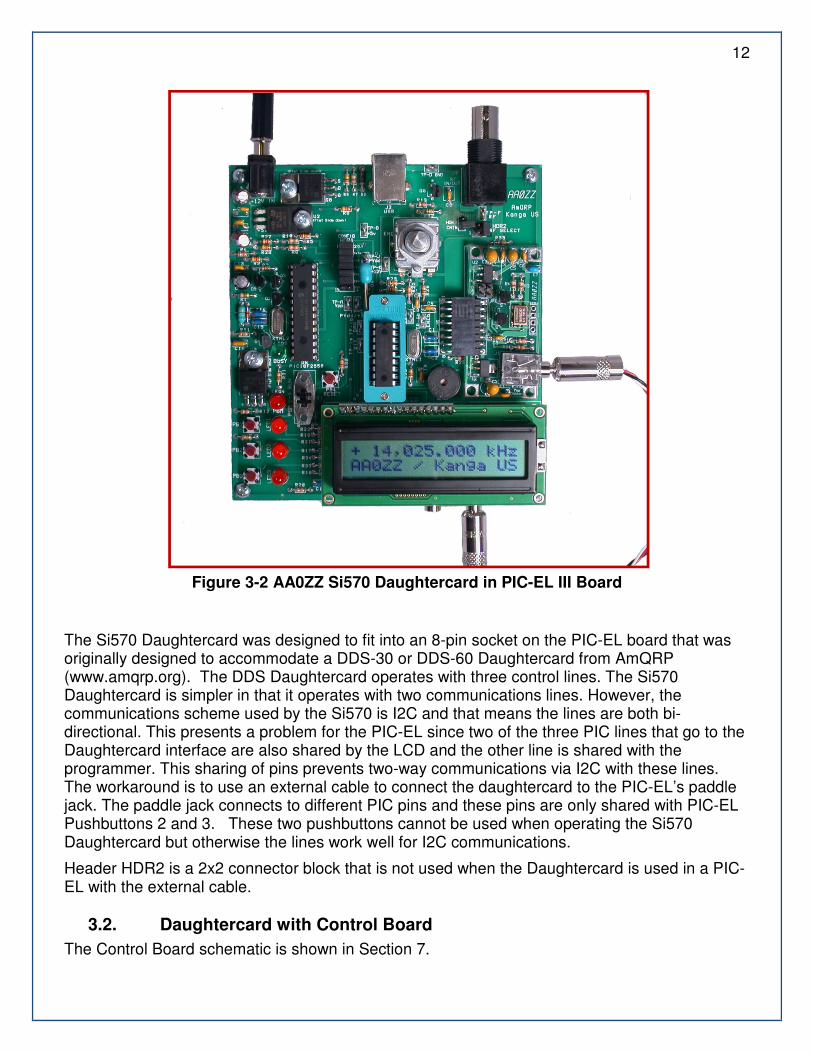
3.1. Daughtercard with PIC-EL
One platform for the Si570 Daughtercard (Figure 3-1) is the AAØZZ PIC-EL board (Figure 3-2). The PIC-EL provides a very convenient platform for experimenting with the software to operate the Si570.
Figure 3-1 AAØZZ Si570 Daughtercard
12
Figure 3-2 AA0ZZ Si570 Daughtercard in PIC-EL III Board
The Si570 Daughtercard was designed to fit into an 8-pin socket on the PIC-EL board that was originally designed to accommodate a DDS-30 or DDS-60 Daughtercard from AmQRP (www.amqrp.org). The DDS Daughtercard operates with three control lines. The Si570 Daughtercard is simpler in that it operates with two communications lines. However, the communications scheme used by the Si570 is I2C and that means the lines are both bi-directional. This presents a problem for the PIC-EL since two of the three PIC lines that go to the Daughtercard interface are also shared by the LCD and the other line is shared with the programmer. This sharing of pins prevents two-way communications via I2C with these lines. The workaround is to use an external cable to connect the daughtercard to the PIC-EL’s paddle jack. The paddle jack connects to different PIC pins and these pins are only shared with PIC-EL Pushbuttons 2 and 3. These two pushbuttons cannot be used when operating the Si570 Daughtercard but otherwise the lines work well for I2C communications.
Header HDR2 is a 2x2 connector block that is not used when the Daughtercard is used in a PIC-EL with the external cable.
3.2. Daughtercard with Control Board
The Control Board schematic is shown in Section 7.

13
When the Daughtercard is used with a dedicated control board instead of a PIC-EL, then header HDR2, the 2x2 connector block, is put into use and the external cable from the Daughtercard’s stereo jack to the driver platform is not needed. Two jumpers are installed in this header block (1 to 4 and 2 to 3) to route the I2C communications through the 8-pin interface connector.
3.3. Daughtercard and Control Board Current Draw
The current required by the Si570 Daughtercard alone is about 100 mA and the total current required by the Daughtercard and the Control Board with LCD active is about 160 mA.
4. PEgen570 Software Application
4.1. 16F88 PIC
The sample application software for the AAØZZ Si570 Daughtercard is called PEgen570. It runs on a simple, inexpensive 16F88 PIC in the PIC-EL board. There are several reasons why the 16F88 was selected for this application instead of the PIC-EL standard 16F628A:
1) Compared to the 16F628A, the 16F88 has more twice as much FLASH memory (for program instructions), 50% more data memory (for variable storage and tables) and twice as much EEPROM memory (non-volatile storage).
2) The 16F88 has an 8 MHz internal oscillator while the 16F628A has a 4 MHz internal oscillator. The extra speed is helpful.
Obviously, the user interface in the PEgen570 app is much simplified from the user interface in my IQPro DDS VFO (2) but the application was simplified such that it could be developed and debugged on the PIC-EL board.
4.2. I2C Communications
Figure 4-1 shows an oscilloscope snapshot of the start of an I2C communication sequence in which the Control Board is sending a frequency update to the Daughtercard. The falling edge of the SDA line (Channel 2) while the SCL line (Channel 1) is high is the I2C method of starting the communications sequence. The next bits show the beginning of the 55 (hex) device address (lower 7 bits) as described in Section 2.7. The clock rate in this implementation is 72 kHz. Since the Si570 can handle speeds up to 400 kHz, this rate is well below the limit.

14
Figure 4-1 I2C SDA/SDC Signals in PEgen570
4.3. Frequency Selection Method
The methods for selecting N1, HS_DIV and calculating RFREQ for every frequency update are many. They can also be very time consuming so optimization is especially important for a small microcontroller. For this reason, the following scheme was developed.
1) Create a list of pairings of all valid N1 and HS_DIV values. Calculate the frequency ranges that can be reached with each of these pairings. The total set of ranges must cover the intended operational range (10 MHz to 157 MHz). Since there are 65 valid N1 values and 6 valid HS_DIV values, there are 390 valid pairings so there are 390 valid frequency ranges in this working table.
2) Examine the working set of pre-calculated frequency ranges for the N1 and HS_DIV pairings and select the minimum number of frequency ranges (bands) which can span the intended operational range of 10 MHz to 157 MHz without gaps while starting and ending on MHz boundaries. Look for the bands with the widest frequency spans while also looking for the lowest N1 values and highest HS_DIV values. The total number of bands is limited by the size of a microcontroller memory bank (96 bytes) and each band entry requires 4 bytes so 24 bands are possible.
3) Create a table which contains entries for the lowest frequency of each of the 24 bands.
4) Create a table of 1-byte entries for the selected bands with each entry being constructed by multiplying the selected N1 by the HS_DIV value and then dividing the product by 2. If the N1 and HS_DIV pairings selected in Step 2 do not fit into 1 byte after they are multiplied and divided by 2, then rework the band selection tables. This may force the selection of some non-optimal N1 and HS_DIV pairings. It also limits the total operational range.

15
Note that no significant figures are lost in dividing the N1 and HS_DIV product by 2 since each valid N1 is an even number (or 1). The RFREQ calculations will take into account the fact that this division by 2 has taken place.
5) Construct the table which contains entries combining Fxtal with N1 and HS_DIV for the
corresponding frequency bands. Each entry will be Fxtal / (N1 * HS_DIV).
6) To calculate RFREQ for a given frequency, retrieve the appropriate table entry containing Fxtal / (N1 * HS_DIV) and divide the desired output frequency by this value. The result of this division must be a 10-bit integer and a 28-bit fraction.
7) Position N1, HS_DIV and RFREQ in the command packet to be sent via I2C to the Si570 control registers. To be exact, store (N1-1) instead of N1 and store the 3-bit index corresponding to the selected HS_DIV value.
This scheme provides a relatively quick Si570 frequency update with some table look-ups and a single division. This single mathematical operation is not a simple one, however, since it divides a 40-bit integer value by a 32-bit integer value and results in a 10-bit integer and a 28-bit fraction positioned such that the five bytes can be directly loaded into the Si570 registers.
4.4. DCO Freeze Handling
Section 2.3 describes the Si570 requirement for a DCO freeze when the updating the frequency when the frequency has moved by more than 3500 ppm (0.35%) from the last freeze frequency.
The software keeps track of the frequency at which the last freeze operation was done. If the difference between the new frequency and the last freeze frequency is more than .35% of the last freeze frequency, the freeze and unfreeze operations is done along with the frequency update. Rather than doing another large division operation, the actual calculation is performed in a simplified manner by determining whether or not the new DCO frequency (Fxtal * RFREQ) has moved by more than .35%. Since Fxtal is a constant, the worst case is found by taking the lower limit of the integer portion of the RFREQ (42) and multiplying by .35%.
42 * .35% = .147
Then, if the software determines the new RFREQ is changed by more than the constant 0.147 from the last freeze, a new freeze is done.
4.5. Major Subroutines of PEgen570
The following sections describe the major subroutines of PEgen570.
4.5.1. Frequency Selection - CalcRFREQ( )
The frequency selection scheme which is used in PEgen570 is described in Section 4-2. This routine is called when a frequency update is needed. The job of this routine is to calculate the 38-bit RFREQ value with a 10-bit integer portion and a 28-bit fractional portion.
RFREQ = (Fout * HS_DIV * N1) / Fxtal
For quick calculation in a small microcontroller, the combination of factors HS_DIV, N1, and Fxtal are scaled, combined and placed in a table indexed by the frequency band number. Now,

16
instead of multiplying Fout by (HS_DIV * N1) / Fxtal, a table look-up is done and a single division operation is performed in which Fout is divided by the reciprocal.
RFREQ = Fout / (Fxtal / (HS_DIV * N1))
This division is a 40-bit by 32-bit operation.
(Note: Typical 32-bit by 32-bit integer division routines result in an integer with the remainder truncated but this division routine performs additional cycles through the division mechanism in order to calculate and retain the fractional portion also.)
Sample calculation:
Fout = 14,025,000 (D60128 Hex)
Fxtal = 114,285,000 (6CFD9C8 Hex)
HS_DIV = 11 (D Hex)
N1 = 34 (22 Hex)
RFREQ (scaled by 2^28) = 2DE5A8555 (Hex)
The RFREQ value is scaled by 2^28. The integer portion is 2D (Hex) and the fractional portion is E5A8555 (Hex). The RFREQ value is scaled in this manner so that it is ready to be loaded into the Si570 registers as shown in Figure 4-2.
7 6 5 4 3 2 1 0 Hex
Si Reg 7 X X X X X X X X 0xXX
Si Reg 8 X X 0 0 0 0 1 0 0x02
Si Reg 9 1 1 0 1 1 1 1 0 0xDE
Si Reg 10 0 1 0 1 1 0 1 0 0x5A
Si Reg 11 1 0 0 0 1 1 0 1 0x85
Si Reg 12 0 1 0 1 0 1 0 0 0x55
SiReg135
SiReg137
HS_DIV_Index [2:0]
(N1-1)[6:0]
RFREQ-integer[37:28]
RFREQ-fractional[27:0]
Figure 4-2 RFREQ in Si570 Registers
Later, when the HS_DIV and N1 values are manipulated into the required form (HS_DIV_Index and N1-1) and added to the Si570 registers, the result is shown in Figure 4-3.
7 6 5 4 3 2 1 0 Hex
Si Reg 7 1 1 1 0 1 0 0 0 0xE8

17
Si Reg 8 0 1 0 0 0 0 1 0 0x42
Si Reg 9 1 1 0 1 1 1 1 0 0xDE
Si Reg 10 0 1 0 1 1 0 1 0 0x5A
Si Reg 11 1 0 0 0 1 1 0 1 0x85
Si Reg 12 0 1 0 1 0 1 0 0 0x55
SiReg135
SiReg137
HS_DIV_Index [2:0]
(N1-1)[6:0]
RFREQ-integer[37:28]
RFREQ-fractional[27:0]
Figure 4-3 RFREQ, HSDIV and N1 in Si570 Registers
4.5.2. Calibration - CalcHSN1Entry( )
The Si570 band tables for PEgen570 are described in Table 4-1. The entries of the table are pre-calculated using the nominal value for the Si570’s internal crystal frequency (114.285 MHz). The table entries (see Section 4.6.1), combining the crystal frequency with other parameters needed to generate RF in that frequency range, are stored in the PIC’s EEPROM and are loaded into the PIC’s volatile memory at power-up. This nominal frequency is almost never perfect, of course, but the Si570 is calibrated in the factory to use corrected parameter values in order to produce the default start-up output frequency of exactly 10.00 MHz. (Other Si570 part numbers use different start-up frequencies.)
By holding Pushbutton 3 down during power-up, the application is directed to retrieve the parameters from the Si570’s non-volatile EEPROM memory. The software then does a “reverse calculation” to find the actual Si570 crystal frequency as determined by the factory to produce 10.00 MHz. After the actual crystal frequency is determined, the table entries are recalculated and copied back to non-volatile EEPROM. When Pushbutton 3 is released, the PIC restarts and populates the tables with the newly calculated values.
1.1.1.1. SetupFxtal( )
This routine is called at calibration time only. It retrieves the Si570 registers from the part, extracts the HS_DIV, N1, and RFREQ values, and uses this formula to find the calibrated crystal frequency as determined during manufacturing. The default frequency for the Si570 being used In this project (570CAC000107DG or 570CBC000107DG) is 10.0 MHz.
Normal frequency formula: Fout = (Fxtal * RFREQ) / (HS_DIV * N1)
Rearranged to give: Fxtal = (Fout * HS_DIV * N1) / RFREQ
The following steps are taken:
1) Extract HSDIV_Index from the Si570 words and convert to HS_DIV 2) Extract (N1-1) from the Si570 words and convert to N1 3) Extract RFREQ from the Si570 words 4) Multiply HS_DIV by N1 5) Divide RFREQ by (HS_DIV * N1)

18
6) Divide by default Fout (10,000,000) Example: Assume these values (Figure 4-4) - as extracted from one SI570 with a 10 MHz start-up frequency:
7 6 5 4 3 2 1 0 Hex
Si Reg 7 0 1 0 1 0 0 1 1 0x53
Si Reg 8 1 1 0 0 0 0 1 0 0xC2
Si Reg 9 1 0 1 0 0 0 0 0 0xA0
Si Reg 10 0 1 0 1 0 0 0 0 0x50
Si Reg 11 1 1 1 0 1 0 0 1 0xE9
Si Reg 12 1 1 1 1 1 1 0 1 0xFD
SiReg135
SiReg137
HS_DIV_Index [2:0]
(N1-1)[6:0]
RFREQ-integer[37:28]
RFREQ-fractional[27:0]
Figure 4-4 RFREQ Extracted From Nonvolatile Memory
The values of the fields of the registrations shown in Figure 4-4 are as follows:
Extracted HS_DIV Index = 2 so HS_DIV is 6 Extracted (N1 - 1) = 4F (hex) which is 79 (dec) so N1 = 80 (dec) Extracted RFREQ Integer = 2A (hex) or 42 (dec) Extracted RFREQ Fractional = 050E9FD (hex) Note that RFREQ is scaled by 2^28. The decimal value can be determined by converting the entire RFREQ value to decimal and then dividing by 2*28.
RFREQ = 2A050E9FD (hex) = 11,279,591,933 (dec) 11,279,591,933 / 2^28 = 11,279,591,933 / 268,435,456 = 42.0197…
1.1.1.2. CalDivide
This routine is used in the SetupFxtal routine. It performs this calculation:
Calculate Fxtal with this formula:
Fxtal = (Fout * HS_DIV * N1) / RFREQ
Form used by routine:
Fxtal = (Fout / RFREQ) * HS_DIV * N1)

19
This requires a 40-bit by 40-bit division followed by a 32-bit by 8 bit multiplication. To retain important significant figures, Fxtal is scaled by multiplying it by 256 before the division so Fout must also be scaled by 256 before performing the calculation.
Fxtal * 256 = ( (10,000,000 * 256) * (6 * 80) / 42.0197…
Fxtal = 114.231984 MHz (compare to 114.285 MHz nominal)
Note that this Fxtal value, extracted from one sample Si570, is only 0.05% from nominal.
This Fxtal value, along with corresponding HS_DIV and N1 values from the band tables (section 4.6.1), is then used to recalculate all values in the HSN1FX table in EEPROM. This table is copied from EEPROM to working (SRAM) memory at power-up so calibrated values will be used for all subsequent RFREQ calculations.
4.6. Si570 Bands
The PEgen570 software is implemented with 24 frequency bands. (Note that these do not correspond to amateur bands.) Most of the parameters that the Si570 requires to produce the desired output RF signal are in tables in program memory. These program memory tables cannot be modified with program instructions. These tables are used by the application by using the band number as an index.
One table is located in the PIC’s data memory and can be modified. This table is populated by extracting values from EEPROM upon power-up. This table consists of 24 entries, each entry containing a starting frequency requiring 4 bytes (see Section 4.4.1). This means that the 24-band table requires 96 bytes of memory. Since the maximum size of any single bank of data memory in the 16F88 (or any “16F” PIC for that matter) is 96 bytes, this determines the maximum number of bands that can easily be handled in the PIC. With additional overhead the size could be expanded and then the upper frequency could be increased. However, the CMOS version of the Si570 (the version that the Daughtercard is designed to use) has a maximum frequency of 160 MHz. This means the current 96-byte table with an upper limit of 157 MHz is reasonable for this Si570 version. The lower limit of the Si570 is 10 MHz and the 96-byte table also handles this limit.
The 24 PEgen570 bands were created by examining the Si570 spec sheet and making calculations with a spreadsheet based on the Si570 parameter requirements. Without getting into the esoteric requirements of the Si570 frequency generating parameters and the formula involving several specific “multipliers”, the Si570 internal crystal frequency and the desired output frequency, the frequency range of each band was calculated. The table was generated in such a way that the major parameters for each band can be pre-calculated and retrieved from tables when changing frequency. This greatly minimizes the number of complex calculations that must be performed for each frequency change.
The 24 PEgen570 bands are defined in Table 4-1 :
BAND Frequency
Range BAND
Frequency Range
BAND Frequency
Range BAND
Frequency Range
0 10 - 11 MHz 6 19 - 21 MHz 12 36 - 41 MHz 18 81 - 90 MHz

20
1 11 - 12 MHz 7 21 - 23 MHz 13 41 - 47 MHz 19 90 - 101 MHz
2 12 - 13 MHz 8 23 - 15 MHz 14 47 - 54 MHz 20 101 - 111
MHz
3 13 - 15 MHz 9 25 - 28 MHz 15 54 - 61 MHz 21 111 - 128
MHz
4 15 - 17 MHz 10 28 - 32 MHz 16 61 - 70 MHz 22 128 - 135
MHz
5 17 - 19 MHz 11 32 - 36 MHz 17 70 - 81 MHz 23 135 - 157
MHz
Table 4-1 PEgen570 Bands
4.6.1. Band Tables
Several tables were constructed, ready for quick access by the frequency update routines. Each table has one entry per band (24 entries).
There is one table in EEPROM with each 4-byte entry containing a combination of HS-DIV, N1 and Fxtal. The table is initially populated with the default crystal frequency (114.285 MHz) but this table is updated during calibration with the actual crystal frequency that is measured and stored in the Si570 during manufacturing.
Entries are constructed and scaled in this manner:
HSN1FX = (Fxtal / (HS_DIV * N1)) * 256
At first glance it would appear that one byte is wasted per entry since multiplying by 256 appears to be simply shifting the original number by 1 byte. It is not that simple. The division operation results in a fractional quotient so multiplying by 256 by continuing the division for 8 additional steps preserves important significant figures of the fractional remainder. Subsequent calculations compensate for this scaling factor.
Example: The entry for Band 0 (covering 10 - 11 MHz) is:
HSN1FX0 = (114,231,984) / (46 * 11)) * 256 = 57,793,256 (dec) = 371DAE8 (hex)
Note that without the scaling factor the default entry would have been:
HSN1FX0 = (114,285,000) / (46 * 11)) * 256 = 57,820,079 (dec) = 37243AF (hex)
There is one table in volatile memory (SRAM). This table is identical to the HSN1FX table in EEPROM. Accessing EEPROM during program execution is relatively slow so this 24-entry table is copied from EEPROM to fast-access program memory at power-up time (4-bytes per entry).
These tables have one entry per band in program (FLASH) memory.

21
1) SiBandTable - A table containing the lower limits (in MHz) of the frequencies for each band. (4-bytes per entry)
2) BandN1Minus1- A table containing the selected N1 value for each band (1 byte per entry) 3) BandHSDIVIndex – The selected HSDIV Index for each band (1 byte per entry) 4) BandHSN1D2 – The selected values of HSDIV and N1 multiplied together and divided by
2 (1 byte per entry). No significant figures are lost in dividing the HS_DIV and N1 product by 2 since each selected N1 is an even number.
4.7. User Interface
The user interface for the PEgen570 application is very simple. It uses two pushbuttons, an encoder, and a 2-line by 16-character LCD. A simple menu for changing configuration is activated via the two pushbuttons.
The “Reset” pushbutton on the PIC-EL board is configured (via the CONFIG statement in the source code) such that it does not perform a microprocessor reset when pressed but to operate as a normal I/O pin instead. This made the pushbutton available for operation and it is needed. To clarify this change in usage, the pushbutton will be referred to as Pushbutton 4 rather than the Reset pushbutton. This means that the PIC-EL board must be powered down and up after loading new software into the PIC before the new program will start executing. Simply moving the slide switch from PGM position to RUN position does not start the PEgen570 program.
The Pushbutton 3 and Pushbutton 4 are the two operational pushbuttons. When running the Si570, each time Pushbutton 3 is pressed and released the tuning digit that is currently being modified by turning the encoder to increase by one digit. It can be advanced up to the 1 MHz position. Similarly, each time Pushbutton 4 is pressed and released, the tuning digit that is currently being modified by turning the encoder to decrease by one digit. The digit that is currently being modified by the encoder is underlined.
When the program is running, pressing and holding Pushbutton 3 for longer than 2 seconds stores the current frequency in EEPROM. This frequency is used as the start-up frequency on subsequent power-ups.
If the user is not interested in FSK operation, that header is available for re-commissioning,
4.8. Menu
A simple menu is used for changing 3 items in the operation.
1) Sideband selection 2) Frequency division for LCD display 3) FSK enable (if FSK is enabled via compile option in source code)
The menu is activated by holding Pushbutton 4 while pushing Pushbutton 3 and then releasing them both. The current mode is shown in character position 1 of line 1 of the LCD. Now the user can update the current selection of each of the three items. Tapping Pushbutton 3 allows the user to cycle through the available options for the current item. Tapping Pushbutton 4 leaves the current item at its last value and advances to the next item in the menu. After the last item has been selected, pressing Pushbutton 4 exits the menu.

22
4.8.1. Sideband Selection
The first menu item that may be selected in the menu is the sideband selection. The user may select one of four sideband modes, USB, LSB, CW+ or CW- .
An external latching relay is engaged or disengaged as the sideband is changed in the menu. PIC output ports RA6 and RA7 attach to HDR5 and HDR6 (pins 15 and 16) respectively. As the sideband is changed in the menu, either RA6 or RA7 is driven high with an 8 mS pulse (with the opposite side being held low) to engage or disengage the external latching relay. The recommended latching relay (TQ2-L-5V – DigiKey part 255-1004-5-ND) requires 14 mA at 5v for 3 mS plus contact bounce time. The latching relay is intended to enable the proper I and Q phases of the transmitter and/or receiver to set the proper sideband.
4.8.2. CW Sidetone During Receive
If the mode is CW+ or CW- , Header HDR7, attached to PIC input port PB7, is monitored by the software to determine whether or not to shift the frequency by the sidetone amount. HDR7 is expected to be set to a low state by external Transmit/Receive circuitry during Receive operations and to a high state during Transmit operations. The software continually monitors the signal at HDR7 and, when is detected to be low while in CW- mode, shifts the frequency down by 600 Hz from the nominal, displayed frequency. If the mode is CW+ and HDR7 is LOW (Receive), the frequency is shifted up by 600 Hz from the nominal, displayed frequency. In either case, whenever HDR7 is detected to be HIGH, indicating Transmit operation, the frequency will be set back to the nominal frequency that is displayed on the LCD.
How fast does it switch? The software looks at the signal on HDR7 often enough to detect and change the frequency within 1.6 mS of HDR7 changing state. That’s fast enough for QSK.
4.8.3. Frequency Division for LCD Display
The PEgen570 application can be configured to display the current Si570 generated frequency or it can be configured to display the Si570 frequency divided by two or four. The divide-by-four option is useful when the signal generator is being used as a signal source for a QSD/QSE (“Tayloe”) mixer. The circuitry for these mixers usually divides the input frequency by four so this software option allows the LCD to display the mixer’s operating frequency.
Tapping PB3 while in this portion of the menu allows the divide-by-x factor to be changed. When the correct factor is selected, press PB4 to advance to the next menu item selection.
4.8.4. FSK Frequency Shift
This menu item is only available and displayed only if the FSK option is enabled via a #DEFINE statement in the source code. The default software does not have FSK enabled.
Tapping PB3 while in this portion of the menu allows the FSK option to be enabled or disabled. When the correct factor is selected, press PB4 to advance to the next menu item selection.

23
If FSK is enabled, the FSK shift size will be used, even if CW+ or CW- is also selected in the menu. FSK takes precedence.
When FSK is active, Header HDR7, attached to PIC input port PB7, is monitored by the software to determine whether or not to shift the frequency by the FSK shift size. The frequency is set to the displayed frequency when the signal on HDR7 is HIGH (the MARK frequency) and is shifted down by 170 Hz when the signal on HDR7 is LOW (the SPACE frequency).
The software looks at the signal on HDR7 often enough to detect and change the frequency within 1.6 mS of HDR7 changing state.
4.9. LCD Display
The first line of the LCD displays the current frequency. The second line is for debug purposes and shows the hex digits for the 6 Si570 register parameter (SiReg7 through SiReg12) starting at LCD position 1. The current band number is displayed in positions 15 and 16 of line 2.
As explained in the Menu section regarding the frequency division selection option, the PEgen570 application can be configured to display the current Si570 frequency or it can be configured to display the Si570 frequency divided by two or four. The divide-by-four option is useful when the signal generator is being used as a signal source for a QSD/QSE (“Tayloe”) mixer. The circuitry for these mixers usually divides the input frequency by four so this software option allows the LCD to display the mixer’s operating frequency.
4.10. Debug Mode
If debug mode is turned on (by enabling the #DEFINE DEBUGON line in the source code and recompiling), the Si570 registers and the current Si570 band number are displayed on the second line of the LCD, as shown in Figure 4-5.
Figure 4-5 RFREQ Displayed on LCD
4.11. Ideas for Future Modification
The source code of this software is available for experimenters to examine - to change and extend to accommodate personal preferences. A couple of items are easy to imagine:

1) Make the CW sidetone frequency changeable. Currently the sidetone frequency is at 600 Hz. (600 Hz is added or subtracted from the base frequency during RECEIVE operation and the base frequency is restored during TRANSMIT operation.)
2) Display additional information on the LCD. RX vs TX, sidetone, etc.
3) Startup frequency is now saved in EEPROM. Add code to save other current settings.
4) Personalize line 2 of the LCD display with call letters.
5. Example Receivers and Transmitters Using the Si570 Programmable PLL
5.1. Block Diagram – CW or SSB Receiver
Figure 5-1
5.2. Schematic - Rx Using the Si570 P
This schematic uses the Si570 P-PLL and a QSD (1) to produce I and Q audio signals for processing in a PC with software such as the Rocky
Make the CW sidetone frequency changeable. Currently the sidetone frequency is at 600 Hz. (600 Hz is added or subtracted from the base frequency during RECEIVE operation and the base frequency is restored during TRANSMIT operation.)
Display additional information on the LCD. RX vs TX, sidetone, etc.
saved in EEPROM. Add code to save other current settings.
Personalize line 2 of the LCD display with call letters.
Example Receivers and Transmitters Using the Si570 Programmable PLL
CW or SSB Receiver
Block Diagram - CW or SSB Receiver
Rx Using the Si570 P-PLL and a PC for Audio Processing
PLL and a QSD (1) to produce I and Q audio signals for processing in a PC with software such as the Rocky (4) SDR software for the
24
Make the CW sidetone frequency changeable. Currently the sidetone frequency is fixed at 600 Hz. (600 Hz is added or subtracted from the base frequency during RECEIVE operation and the base frequency is restored during TRANSMIT operation.)
saved in EEPROM. Add code to save other current settings.
Example Receivers and Transmitters Using the Si570 Programmable PLL
PLL and a PC for Audio Processing
PLL and a QSD (1) to produce I and Q audio signals for SDR software for the SoftRock (5) radio.

25
Figure 5-2 Schematic - Rx Using the Si570 P-PLL and a PC for Audio Processing
5.3. Schematic - KK7B MicroR2 Receiver Using the Si570 P-PLL
This schematic shows the Si570 LO and a QSD (1) with a KK7B MicroR2 (3) LNA and audio processing section.
Figure 5-3 Schematic – Si570 P-PLL with QSD and KK7B MicroR2 LNA and Audio
(See my web page for enlarged picture of schematic – www.cbjohn.com/aa0zz)

5.4. Block Diagram - CW Transmitter
Figure 5
5.5. Schematic - 40-Meter CW Transmitter Using the Si570 P
Figure 5-5 Schematic
5.6. Block Diagram - 40
This block diagram shows the Si570
CW Transmitter
5-4 Block Diagram - CW Transmitter
Meter CW Transmitter Using the Si570 P
Schematic - 40-Meter CW Transmitter Using the Si570 P
40-Meter SSB Transmitter Using the Si570 P
This block diagram shows the Si570 LO and a QSD (1) in a SSB transmitter.
26
Meter CW Transmitter Using the Si570 P-PLL
Meter CW Transmitter Using the Si570 P-PLL
Meter SSB Transmitter Using the Si570 P-PLL

Figure 5-6 Block Diagram
Block Diagram - 40-Meter SSB Transmitter Using the Si570 P
27
Meter SSB Transmitter Using the Si570 P-PLL
28
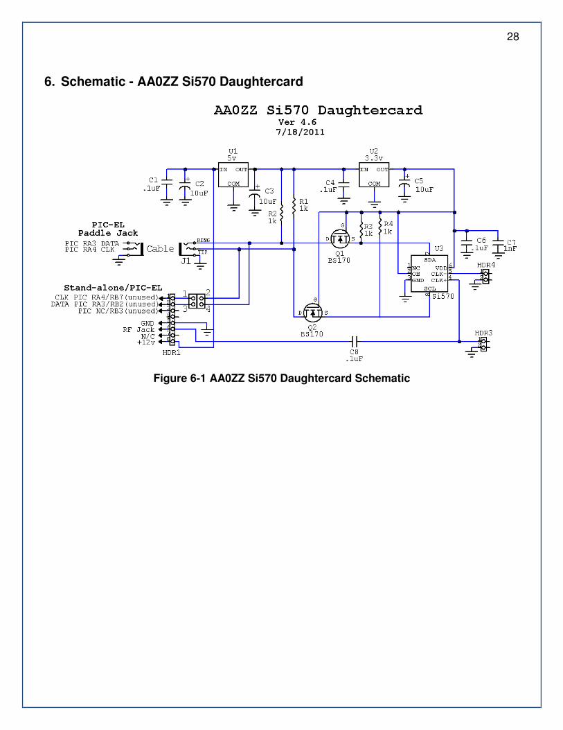
6. Schematic - AA0ZZ Si570 Daughtercard
Figure 6-1 AA0ZZ Si570 Daughtercard Schematic
29
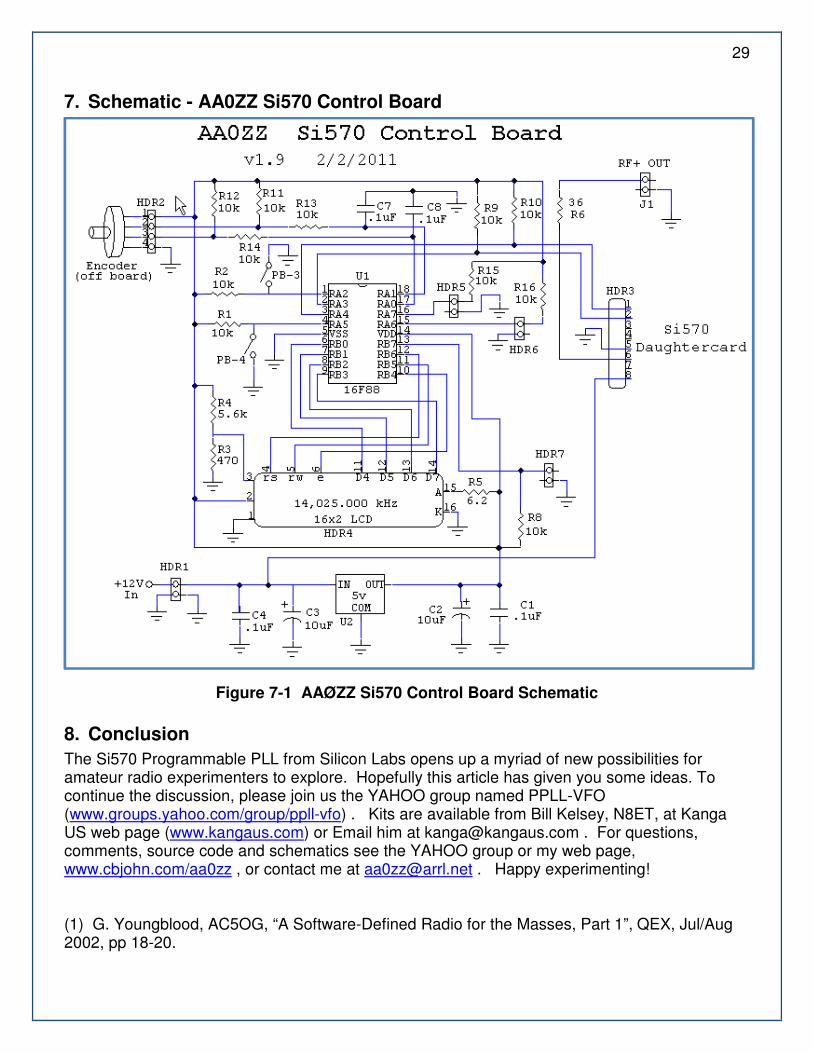
7. Schematic - AA0ZZ Si570 Control Board
Figure 7-1 AAØZZ Si570 Control Board Schematic
8. Conclusion
The Si570 Programmable PLL from Silicon Labs opens up a myriad of new possibilities for amateur radio experimenters to explore. Hopefully this article has given you some ideas. To continue the discussion, please join us the YAHOO group named PPLL-VFO (www.groups.yahoo.com/group/ppll-vfo) . Kits are available from Bill Kelsey, N8ET, at Kanga US web page (www.kangaus.com) or Email him at [email protected] . For questions, comments, source code and schematics see the YAHOO group or my web page, www.cbjohn.com/aa0zz , or contact me at [email protected] . Happy experimenting! (1) G. Youngblood, AC5OG, “A Software-Defined Radio for the Masses, Part 1”, QEX, Jul/Aug 2002, pp 18-20.

30
(2) C. Johnson, AA0ZZ, “The IQPro: A High Performance Quadrature DDS VFO”, QEX, May/June 2006, pp 8-22.
(3) R. Campbell, KK7B, “The MicroR2 – an Easy to Build ‘Single Signal’ SSB or CW Receiver”, QST, Oct 2006.
(4) A. Shovkoplyas, VE3NEA, http://www.dxatlas.com/Rocky/
(5) T. Parks, KB9YIG, http://www.kb9yig.com/