programmable soft-start • power good function ld59150 · 1 diagram figure 2. block diagram vin...
TRANSCRIPT

DFN10 3 x 3wettable flanks
Features• Designed for automotive applications• Dual supply pins
– VIN: 0.8 V to 5.5 V– VBIAS: 2.7 V to 5.5 V
• VOUT range: 0.8 V to 3.6 V• Ultra low-dropout: 65 mV typ. (125 mV max.) at 1.5 A• High VOUT accuracy
– 0.5% typ. at Tamb
– 2% max.• Power Good function• Programmable soft-start• Thermal shutdown• Current limitation circuit• Adjustable output voltage• Stable with low ESR output capacitor (> 2.2 µF)• Available in DFN10 3 x 3 mm package with wettable flanks• Operating temperature range: - 40 °C + 125 °C
Applications• Automotive and industrial post regulation• Generic POL• Automotive and industrial ASICs and FPGA supply• Telecom infrastructure• A.D.A.S. (advanced driver-assistance systems)
DescriptionThe LD59150 is a 1.5 A LDO regulator, designed for being used in variousenvironments.
The NMOS topology allows RDS(on) of the pass-element to be reduced, which resultsin a very small dropout voltage even with very low input supply voltage.
Output voltage can be adjusted from 0.8 to 3.6 V, by means of an external resistordivider.
The programmable soft-start circuit offers the possibility to control the inrush currentat startup providing a monotonic supply voltage to the load.
The LD59150 has enable pin to turn on/off (EN) the regulator and Power Good tomonitor the regulated output voltage (PG).
Combination of both can be used to set a desired power sequence in case of multipleregulated rails.
The LD59150 embeds protection functions, such as: current limit and thermalshutdown.
Maturity status link
LD59150
Device summary
Order code LD59150PURY
Marking 595A
Output voltage Adjustable
1.5 A low-dropout linear regulator with programmable soft-start
LD59150
Datasheet
DS12455 - Rev 3 - June 2018For further information contact your local STMicroelectronics sales office.
www.st.com

1 Diagram
Figure 2. Block diagram
VIN
GND
VOUT
OPAMP
EN
Currentlimit
Bandgap reference
ThermalprotectionEnable
FB
UVLOVBIAS
SS
Soft Start
+ + −
+- 0.9 x VREF
PG
LD59150Diagram
DS12455 - Rev 3 page 2/21

2 Pin configuration
Figure 3. Pin connection (top view)
1
2
3
4
5
10
9
8
7
6
Exposedpad
DFN10 - 3 x 3
Table 1. Pin description
Pin n° Symbol Function
1, 2 VIN Input pin
3 PG Power Good
4 VBIAS Bias supply pin
5 EN
Enable pin logic input:
low = shutdown, high = active
Don't leave floating
6 GND Ground
7 SS Soft-start
8 FB Feedback pin
9, 10 VOUT Regulated output
Exp. pad Exposed pad Must be connected to GND
LD59150Pin configuration
DS12455 - Rev 3 page 3/21

3 Typical application
Figure 4. Typical application circuit
VIN
GND
VIN
VBIAS
C IN
VOUTVOUT
COUT
LD5915 0E N
S S
CBIAS
VBIAS
CSS
R1
R2
FB
PGR PG
LD59150Typical application
DS12455 - Rev 3 page 4/21

4 Maximum ratings
Table 2. Absolute maximum ratings
Symbol Parameter Value Unit
VIN Input voltage pin -0.3 to 6 V
VBIAS Bias supply pin - 0.3 to 6 V
VOUT DC output voltage -0.3 to VIN + 0.3 V
VEN Enable input voltage -0.3 to 6 V
VADJ Adjustable pin voltage -0.3 to 6 V
VSS Soft-start pin -0.3 to 6 V
VPG Power Good pin -0.3 to 6 V
IOUT Output current Internally limited mA
PDIS Maximum power dissipation Refer to table 3 W
IPG Power Good sink current 0 to 1.5 mA
TST Storage temperature range -55 to 150 °C
TJ Operating junction temperature range -40 to 150 °C
Note: Absolute maximum ratings are those values beyond which damage to the device may occur. Functionaloperation under these conditions is not implied. All values are referred to GND.
Table 3. Thermal data
Symbol Parameter Value Unit
RthJA Thermal resistance junction-ambient 47.5 °C/W
RthJC Thermal resistance junction-case 8 °C/W
Note: Thermal resistance refers to 4 layer JEDEC PCB (2S2P) test board with thermal vias.
Table 4. ESD data
Symbol Parameter DFN10 3 x 3 Unit
HBM Human body model ± 2000 V
CDM Charged device model ± 750 V
LD59150Maximum ratings
DS12455 - Rev 3 page 5/21

5 Electrical characteristics
TJ = - 40 °C to + 125 °C, typical values refer to TJ = + 25 °C, VIN = VOUT + 0.3 V, VEN = 1.1 V, VBIAS = 5 V, IOUT =50 mA, CIN = COUT = 10 µF, CBIAS = 0.1 µF, CSS = 1 nF unless otherwise specified.
Table 5. Electrical characteristics
Symbol Parameter Test conditions Min. Typ. Max. Unit
VIN Operating input voltageVOUT+Vdrop
5.5 V
VBIAS Bias pin voltage 2.7 5.5 V
VREF Reference voltage T = + 25 °C 0.796 0.8 0.804 V
VOUT
Range VIN = 5.5 V, IOUT = 1.5 A VREF 3.6 V
Accuracy 50 mA < IOUT < 1.5 A 2.97 V < VBIAS < 5.5 V -2 ± 0.5 +2 %
Line regulation VOUT(nom) + 0.3 V < VIN < 5.5 V 0.01 %/V
Load regulation 50 mA < IOUT < 1.5 A 0.02 %/A
Vdrop (1)VIN dropout voltage IOUT = 1.5 A, VBIAS - VOUT > 3.25 V 65 125 mV
VBIAS dropout voltage IOUT = 1.5 A VIN = VBIAS 0.92 1.1 V
Icl (2) Current limit VOUT = 80% x VOUT(nom) 2.0 3 5.5 A
IBIAS Bias pin current 0.88 1.5 mA
ISHDN Shutdown supply current VEN < 0.4 V (measured through GND) 1 50 µA
IFB Feedback pin current -1 0.001 +1 µA
PSRR
Power supply rejection (VINto VOUT)
f = 1 kHz, IOUT = 1.5 A VIN = 1.8 V,VOUT = 1.5 V 70
dBf = 300 kHz, IOUT = 1.5 A VIN = 1.8 V,
VOUT = 1.5 V 30
Power supply rejection (VBIASto VOUT)
f = 1 kHz, IOUT = 1.5 A VIN = 1.8 V,VOUT = 1.5 V 75
dBf = 300 kHz, IOUT = 1.5 A VIN = 1.8 V,
VOUT = 1.5 V 40
Noise Output noise voltagef = 100 Hz to 100 kHz, IOUT = 1.5 A,
CSS = 1 nF25xVOUT µVRMS
ISS Soft start charging current VSS = 0.4 V 0.44 µA
Tstr Min. startup time IOUT = 1 A, CSS = floating 100 µsec
VEN-H Enable input high 1.1 5.5 V
VEN-L Enable input low 0 0.4 V
VEN-Hyst Enable hysteresis 50 mV
TDG Enable deglitch time 20 µsec
IEN Enable pin current VEN = 5 V 0.1 1 µA
VIT Power Good threshold VOUT decreasing 85 90 94 %VOUT
VHYS Power Good hysteresis 3 %VOUT
LD59150Electrical characteristics
DS12455 - Rev 3 page 6/21

Symbol Parameter Test conditions Min. Typ. Max. Unit
VPG-L Power good low voltage 0.3 V
ILK Power good leakage VPG = 5.25 V, VOUT > VIT 0.1 1 µA
TSDThermal shutdown
temperatureHigh temp threshold 165
°CThermal hysteresis 20
1. Dropout is defined as the voltage drop when VOUT is 3% below nominal voltage.
2. Maximum value is guaranteed by design and not tested in production.
LD59150Electrical characteristics
DS12455 - Rev 3 page 7/21

6 Application information
6.1 Output voltage settingThe output voltage can be set from 0.8 V (VREF) up to the input voltage minus the voltage drop across the passtransistor (dropout voltage), by connecting a resistor divider between the feedback (FB) pin and the output, thusallowing remote voltage sensing.With reference to the typical circuit shown in Figure 3, the resistor divider can be designed by using the followingequation:
VOUT = VREF (1 + R1/R2), with VREF = 0.8 V typ. (1)
It is recommended to use resistors with values in the range from 5 kΩ to 100 kΩ. Lower values can also besuitable, but current consumption increases.The following table shows examples of R1, R2 choices, among standard 1% resistors, to obtain the most commonoutput voltages.
Table 6. Resistor divider settings for common output voltages
VOUT R1 R2
0.8 (VFB) Short Open
0.9 0.619 4.99
1 1.13 4.53
1.05 1.37 4.42
1.1 1.87 4.99
1.2 2.49 4.99
1.5 4.12 4.75
1.8 3.57 2.87
2.5 3.57 1.69
3.3 3.57 1.15
6.2 Soft-start time programmingThe LD59150 provides a monotonic soft-start feature, which is useful in those applications requiring controlledpower-up sequences and low inrush current during turn-on phase.The soft-start time, defined as the duration of output voltage ramp, from enable pin assertion to Power Good flagreleasing, can be adjusted by the user by means of an external capacitor (CSS).CSS capacitor is charged with constant current (ISS) and its voltage compared to the internal voltage reference,therefore the soft-start time can be calculated as follows:
tSS = (VREF x CSS) / ISS (2)
with VREF = 0.8 V typ., ISS = 0.44 µA typ.Good quality, low leakage ceramic capacitors are recommended for CSS.
6.3 Power GoodPower Good function provides a flag showing that the output voltage is in the correct range. Power Good signal isavailable on the PG open-drain pin.A partition of the output voltage (via the output resistor divider), is sensed at the feedback pin.When the output voltage surpasses VIT + VHYS Power Good pin is set to high impedance. When VOUT falls belowVIT, the Power Good pin is pulled low.
LD59150Application information
DS12455 - Rev 3 page 8/21

If the device is disabled (EN pin low) the PG signal is set to low state.Power Good function requires an external pull-up resistor, which may be connected to any potential lower than5.5 V. PG pin typical current capability is up to 1 mA, so it is advisable to choose a pull-up resistor in the rangefrom 10 kΩ to 1 MΩ. If Power Good function is not used, PG pin has to remain floating.
6.4 Protection featuresCurrent limitThe LD59150 embeds a constant-current limit circuit, which acts in case of overload or short-circuit on the output,clamping the load current to a safe value (typ. 3 A).Normal operation is restored if the overload disappears, but prolonged operation in current limit may lead to highpower dissipation inside the LDO and subsequently to thermal shutdown.Thermal potectionAn internal thermal feedback loop disables the output voltage if the die temperature reaches approximately 165°C. This feature protects the device from excessive temperature that could lead to permanent damage of theLDO.Once the thermal protection is triggered and the device is shut down, normal operation is automatically recoveredif the die temperature falls below 145 °C (thermal protection hysteresis of 20 °C typically).Current and thermal limit protections are designed to protect the LDO from excessive power dissipation and notintended to replace a proper thermal and electrical design of the application. Continuous operation above themaximum ratings may lead to permanent damage to the device.
6.5 Power dissipationAn accurate PCB design is recommended, to ensure that the device internal junction temperature is kept below150 °C, in all the operating condition. The thermal energy generated by the device flows from the die surface tothe PCB copper area through the package leads.The PCB copper area acts as a heat sink. The footprint copper pads should be as wide as possible to spread anddissipate the heat to the surrounding environment. Thermal micro-vias to the inner or backside copper layersimprove the overall thermal performance of the device.The power dissipation of the LDO depends on the input voltage, output voltage and output current and is givenby:
PD = (VIN - VOUT) x IOUT (3)
The junction temperature of the device is:TJ_MAX = TA + RthJA x PD (4)
where: TJ_MAX is the maximum allowable junction temperature of the die, 150 °C; TA is the ambient temperature;RthJA is the thermal resistance junction-to-ambient.With the above equation it is possible to calculate the maximum allowable power dissipation, therefore themaximum load current for a certain voltage drop. Appropriate de-rating of the operating condition should beapplied accordingly.
LD59150Protection features
DS12455 - Rev 3 page 9/21

7 Typical performance characteristics
TJ = 25 °C, VIN = VOUT + 0.3 V, VBIAS = 5 V, VOUT = VREF, VEN = 1.1 V, IOUT = 50 mA, CIN = COUT = 10 µF,CBIAS = 0.1 µF, CSS = 1 nF unless otherwise specified.
Figure 5. Output voltage vs. temperature and VBIAS(IOUT = 50 mA)
0.780
0.785
0.790
0.795
0.800
0.805
0.810
0.815
0.820
-60 -40 -20 0 20 40 60 80 100 120 140
V OU
T [V
]
Temperature [ºC]
VBIAS = 2.97V
VBIAS = 5.5V
VIN = 1.1 V , IOUT = 50 mA, VOUT = VREF
Figure 6. Output voltage vs. temperature and VBIAS(IOUT = 1.5 A)
0.780
0.785
0.790
0.795
0.800
0.805
0.810
0.815
0.820
-60 -40 -20 0 20 40 60 80 100 120 140
V OU
T [V
]
Temperature [ºC]
VBIAS = 2.97V
VBIAS = 5.5V
VIN =1.1 V , IOUT = 1.5 A, VOUT = VREF
Figure 7. Line regulation vs. temperature
-0.200
-0.150
-0.100
-0.050
0.000
0.050
0.100
0.150
0.200
-60 -40 -20 0 20 40 60 80 100 120 140
Line
regu
latio
n [%
/V]
Temperature [ºC]
VIN = 1.1 V to 5.5 V
Figure 8. Load regulation vs. temperature
-0.200
-0.150
-0.100
-0.050
0.000
0.050
0.100
0.150
0.200
-60 -40 -20 0 20 40 60 80 100 120 140
Load
regu
latio
n [%
/A]
Temperature [ºC]
IOUT = 50 mA to 1.5 A
LD59150Typical performance characteristics
DS12455 - Rev 3 page 10/21

Figure 9. Bias pin current vs. temperature
0.000
0.200
0.400
0.600
0.800
1.000
1.200
1.400
1.600
1.800
2.000
-60 -40 -20 0 20 40 60 80 100 120 140
I BIA
S[m
A]
Temperature [ºC]
Figure 10. Soft-start charging current vs. temperature
0.000
0.100
0.200
0.300
0.400
0.500
0.600
0.700
0.800
-60 -40 -20 0 20 40 60 80 100 120 140
I SS
[µA]
Temperature [ºC]
Figure 11. Current limit vs. temperature
0
1
2
3
4
5
6
-60 -40 -20 0 20 40 60 80 100 120 140
I CL
[A]
Temperature [ºC]
Figure 12. VIN dropout voltage vs. temperature (IOUT = 1.5 A)
20
30
40
50
60
70
80
90
100
110
120
-60 -40 -20 0 20 40 60 80 100 120 140
V DR
OP(
VIN
)[m
V]
Temperature [ºC]
Figure 13. VBIAS dropout voltage vs. temperature(IOUT = 1.5 A)
500
600
700
800
900
1000
1100
1200
-60 -40 -20 0 20 40 60 80 100 120 140
V DR
OP(
VBIA
S)[m
V]
Temperature [ºC]
Figure 14. VBIAS PSRR vs. frequency (VIN = 1.8 V,VOUT = 1.2 V)
05
101520253035404550556065707580859095
100
100 1,000 10,000 100,000 1,000,000 10,000,000
PSRR
(dB)
Frequency (Hz)
IOUT= 1.5A
IOUT=100mA
CIN = COUT = 10µF, CBIAS = 0.1µF, CSS = 1nF, VIN = 1.8V, VOUT = 1.2V, VBIAS = 5V + VRipple
LD59150Typical performance characteristics
DS12455 - Rev 3 page 11/21

Figure 15. VIN PSRR vs. frequency (VIN = 1.8 V, VOUT = 1.2 V)
05
101520253035404550556065707580859095
100
100 1,000 10,000 100,000 1,000,000 10,000,000
PSR
R (d
B)
Frequency (Hz)
IOUT=1.5A
IOUT= 100mA
CIN = COUT = 10µF, CBIAS = 0.1µF, CSS = 1nF, VIN = 1.8V + VRipple , VOUT = 1.2V, VBIAS = 5V
Figure 16. Noise spectral density
0.001
0.010
0.100
1.000
10.000
100 1000 10000 100000 1000000 10000000
Out
put N
oise
Den
sity:
[µV/
sqrt
(Hz)
]
Frequency: f [kHz]
No LoadIout=500mAIout=1AIout=1.5A
CIN = COUT = 10μF, CSS = 1nF, CBIAS = 0.1µF, VIN = 1.25V, VOUT = 1V, VBIAS = 5V
Figure 17. Line transient Figure 18. Load transient
Figure 19. Turn-on time (CSS = 0 nF) Figure 20. Turn-on time (CSS = 1 nF)
LD59150Typical performance characteristics
DS12455 - Rev 3 page 12/21

Figure 21. Turn-on time (CSS = 2.2 nF) Figure 22. Turn-on time (CSS = 10 nF)
LD59150Typical performance characteristics
DS12455 - Rev 3 page 13/21

8 Package information
In order to meet environmental requirements, ST offers these devices in different grades of ECOPACK®
packages, depending on their level of environmental compliance. ECOPACK® specifications, grade definitionsand product status are available at: www.st.com. ECOPACK® is an ST trademark.
8.1 [Package name] package information
Figure 23. DFN10 3 x 3 package outline
BOTTOM VIEW
SIDE VIEW
TOP VIEW
DETAIL A
SIDE VIEW
LD59150Package information
DS12455 - Rev 3 page 14/21

Table 7. DFN10 3 x 3 mechanical data
Dim.mm
Min. Typ. Max.
A 0.80 0.85 0.90
A1 0.00 0.05
A3 0.203 Ref.
b 0.20 0.25 0.30
D 2.95 3.00 3.05
D2 2.30 2.40 2.50
e 0.50 BSC
E 2.95 3.00 3.05
E2 1.55 1.65 1.75
E3 0.25 Ref.
E4 0.50 Ref.
L 0.30 0.40 0.50
K 0.275 Ref.
N 10
aaa 0.15
bbb 0.10
ccc 0.10
ddd 0.05
eee 0.08
Figure 24. DFN10 3 x 3 recommended footprint
LD59150DFN10 3 x 3 package information
DS12455 - Rev 3 page 15/21

Figure 25. DFN10 3 x 3 tape and reel
LD59150DFN10 3 x 3 package information
DS12455 - Rev 3 page 16/21
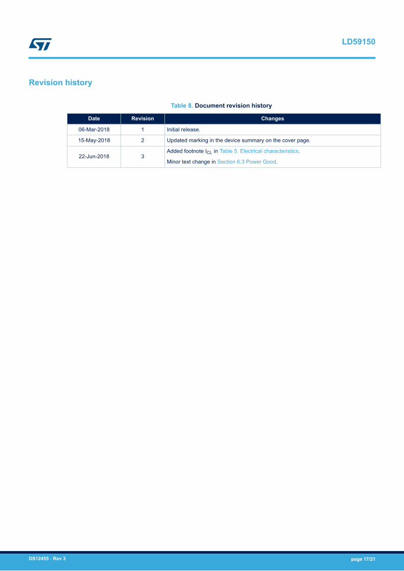
Revision history
Table 8. Document revision history
Date Revision Changes
06-Mar-2018 1 Initial release.
15-May-2018 2 Updated marking in the device summary on the cover page.
22-Jun-2018 3Added footnote ICL in Table 5. Electrical characteristics.
Minor text change in Section 6.3 Power Good.
LD59150
DS12455 - Rev 3 page 17/21

Contents
1 Diagram . . . . . . . . . . . . . . . . . . . . . . . . . . . . . . . . . . . . . . . . . . . . . . . . . . . . . . . . . . . . . . . . . . . . . . . . . . .2
2 Pin configuration . . . . . . . . . . . . . . . . . . . . . . . . . . . . . . . . . . . . . . . . . . . . . . . . . . . . . . . . . . . . . . . . . .3
3 Typical application. . . . . . . . . . . . . . . . . . . . . . . . . . . . . . . . . . . . . . . . . . . . . . . . . . . . . . . . . . . . . . . . .4
4 Maximum ratings . . . . . . . . . . . . . . . . . . . . . . . . . . . . . . . . . . . . . . . . . . . . . . . . . . . . . . . . . . . . . . . . . .5
5 Electrical characteristics. . . . . . . . . . . . . . . . . . . . . . . . . . . . . . . . . . . . . . . . . . . . . . . . . . . . . . . . . . .6
6 Application information. . . . . . . . . . . . . . . . . . . . . . . . . . . . . . . . . . . . . . . . . . . . . . . . . . . . . . . . . . . .8
6.1 Output voltage setting. . . . . . . . . . . . . . . . . . . . . . . . . . . . . . . . . . . . . . . . . . . . . . . . . . . . . . . . . . . 8
6.2 Soft-start time programming . . . . . . . . . . . . . . . . . . . . . . . . . . . . . . . . . . . . . . . . . . . . . . . . . . . . . 8
6.3 Power Good. . . . . . . . . . . . . . . . . . . . . . . . . . . . . . . . . . . . . . . . . . . . . . . . . . . . . . . . . . . . . . . . . . . 8
6.4 Protection features . . . . . . . . . . . . . . . . . . . . . . . . . . . . . . . . . . . . . . . . . . . . . . . . . . . . . . . . . . . . . 9
6.5 Power dissipation . . . . . . . . . . . . . . . . . . . . . . . . . . . . . . . . . . . . . . . . . . . . . . . . . . . . . . . . . . . . . . 9
7 Typical performance characteristics . . . . . . . . . . . . . . . . . . . . . . . . . . . . . . . . . . . . . . . . . . . . . .10
8 Package information. . . . . . . . . . . . . . . . . . . . . . . . . . . . . . . . . . . . . . . . . . . . . . . . . . . . . . . . . . . . . .14
8.1 [Package name] package information . . . . . . . . . . . . . . . . . . . . . . . . . . . . . . . . . . . . . . . . . . . . 14
Revision history . . . . . . . . . . . . . . . . . . . . . . . . . . . . . . . . . . . . . . . . . . . . . . . . . . . . . . . . . . . . . . . . . . . . . . .17
LD59150Contents
DS12455 - Rev 3 page 18/21

List of tablesTable 1. Pin description. . . . . . . . . . . . . . . . . . . . . . . . . . . . . . . . . . . . . . . . . . . . . . . . . . . . . . . . . . . . . . . . . . . . . . 3Table 2. Absolute maximum ratings . . . . . . . . . . . . . . . . . . . . . . . . . . . . . . . . . . . . . . . . . . . . . . . . . . . . . . . . . . . . . 5Table 3. Thermal data. . . . . . . . . . . . . . . . . . . . . . . . . . . . . . . . . . . . . . . . . . . . . . . . . . . . . . . . . . . . . . . . . . . . . . . 5Table 4. ESD data . . . . . . . . . . . . . . . . . . . . . . . . . . . . . . . . . . . . . . . . . . . . . . . . . . . . . . . . . . . . . . . . . . . . . . . . . 5Table 5. Electrical characteristics . . . . . . . . . . . . . . . . . . . . . . . . . . . . . . . . . . . . . . . . . . . . . . . . . . . . . . . . . . . . . . . 6Table 6. Resistor divider settings for common output voltages . . . . . . . . . . . . . . . . . . . . . . . . . . . . . . . . . . . . . . . . . . . 8Table 7. DFN10 3 x 3 mechanical data . . . . . . . . . . . . . . . . . . . . . . . . . . . . . . . . . . . . . . . . . . . . . . . . . . . . . . . . . . 15Table 8. Document revision history . . . . . . . . . . . . . . . . . . . . . . . . . . . . . . . . . . . . . . . . . . . . . . . . . . . . . . . . . . . . . 17
LD59150List of tables
DS12455 - Rev 3 page 19/21

List of figuresFigure 2. Block diagram . . . . . . . . . . . . . . . . . . . . . . . . . . . . . . . . . . . . . . . . . . . . . . . . . . . . . . . . . . . . . . . . . . . . 2Figure 3. Pin connection (top view) . . . . . . . . . . . . . . . . . . . . . . . . . . . . . . . . . . . . . . . . . . . . . . . . . . . . . . . . . . . . . 3Figure 4. Typical application circuit . . . . . . . . . . . . . . . . . . . . . . . . . . . . . . . . . . . . . . . . . . . . . . . . . . . . . . . . . . . . . 4Figure 5. Output voltage vs. temperature and VBIAS (IOUT = 50 mA) . . . . . . . . . . . . . . . . . . . . . . . . . . . . . . . . . . . . . 10Figure 6. Output voltage vs. temperature and VBIAS (IOUT = 1.5 A) . . . . . . . . . . . . . . . . . . . . . . . . . . . . . . . . . . . . . . 10Figure 7. Line regulation vs. temperature. . . . . . . . . . . . . . . . . . . . . . . . . . . . . . . . . . . . . . . . . . . . . . . . . . . . . . . . 10Figure 8. Load regulation vs. temperature . . . . . . . . . . . . . . . . . . . . . . . . . . . . . . . . . . . . . . . . . . . . . . . . . . . . . . . 10Figure 9. Bias pin current vs. temperature . . . . . . . . . . . . . . . . . . . . . . . . . . . . . . . . . . . . . . . . . . . . . . . . . . . . . . . 11Figure 10. Soft-start charging current vs. temperature. . . . . . . . . . . . . . . . . . . . . . . . . . . . . . . . . . . . . . . . . . . . . . . . 11Figure 11. Current limit vs. temperature . . . . . . . . . . . . . . . . . . . . . . . . . . . . . . . . . . . . . . . . . . . . . . . . . . . . . . . . . 11Figure 12. VIN dropout voltage vs. temperature (IOUT = 1.5 A) . . . . . . . . . . . . . . . . . . . . . . . . . . . . . . . . . . . . . . . . . . 11Figure 13. VBIAS dropout voltage vs. temperature (IOUT = 1.5 A). . . . . . . . . . . . . . . . . . . . . . . . . . . . . . . . . . . . . . . . . 11Figure 14. VBIAS PSRR vs. frequency (VIN = 1.8 V, VOUT = 1.2 V) . . . . . . . . . . . . . . . . . . . . . . . . . . . . . . . . . . . . . . . 11Figure 15. VIN PSRR vs. frequency (VIN = 1.8 V, VOUT = 1.2 V) . . . . . . . . . . . . . . . . . . . . . . . . . . . . . . . . . . . . . . . . . 12Figure 16. Noise spectral density . . . . . . . . . . . . . . . . . . . . . . . . . . . . . . . . . . . . . . . . . . . . . . . . . . . . . . . . . . . . . . 12Figure 17. Line transient . . . . . . . . . . . . . . . . . . . . . . . . . . . . . . . . . . . . . . . . . . . . . . . . . . . . . . . . . . . . . . . . . . . . 12Figure 18. Load transient . . . . . . . . . . . . . . . . . . . . . . . . . . . . . . . . . . . . . . . . . . . . . . . . . . . . . . . . . . . . . . . . . . . 12Figure 19. Turn-on time (CSS = 0 nF) . . . . . . . . . . . . . . . . . . . . . . . . . . . . . . . . . . . . . . . . . . . . . . . . . . . . . . . . . . . 12Figure 20. Turn-on time (CSS = 1 nF) . . . . . . . . . . . . . . . . . . . . . . . . . . . . . . . . . . . . . . . . . . . . . . . . . . . . . . . . . . . 12Figure 21. Turn-on time (CSS = 2.2 nF) . . . . . . . . . . . . . . . . . . . . . . . . . . . . . . . . . . . . . . . . . . . . . . . . . . . . . . . . . . 13Figure 22. Turn-on time (CSS = 10 nF) . . . . . . . . . . . . . . . . . . . . . . . . . . . . . . . . . . . . . . . . . . . . . . . . . . . . . . . . . . 13Figure 23. DFN10 3 x 3 package outline . . . . . . . . . . . . . . . . . . . . . . . . . . . . . . . . . . . . . . . . . . . . . . . . . . . . . . . . . 14Figure 24. DFN10 3 x 3 recommended footprint . . . . . . . . . . . . . . . . . . . . . . . . . . . . . . . . . . . . . . . . . . . . . . . . . . . . 15Figure 25. DFN10 3 x 3 tape and reel . . . . . . . . . . . . . . . . . . . . . . . . . . . . . . . . . . . . . . . . . . . . . . . . . . . . . . . . . . . 16
LD59150List of figures
DS12455 - Rev 3 page 20/21

IMPORTANT NOTICE – PLEASE READ CAREFULLY
STMicroelectronics NV and its subsidiaries (“ST”) reserve the right to make changes, corrections, enhancements, modifications, and improvements to STproducts and/or to this document at any time without notice. Purchasers should obtain the latest relevant information on ST products before placing orders. STproducts are sold pursuant to ST’s terms and conditions of sale in place at the time of order acknowledgement.
Purchasers are solely responsible for the choice, selection, and use of ST products and ST assumes no liability for application assistance or the design ofPurchasers’ products.
No license, express or implied, to any intellectual property right is granted by ST herein.
Resale of ST products with provisions different from the information set forth herein shall void any warranty granted by ST for such product.
ST and the ST logo are trademarks of ST. All other product or service names are the property of their respective owners.
Information in this document supersedes and replaces information previously supplied in any prior versions of this document.
© 2018 STMicroelectronics – All rights reserved
LD59150
DS12455 - Rev 3 page 21/21