progress report #5 september 1, 1999 – august 31,...
TRANSCRIPT

1
Progress Report #5 September 1, 1999 – August 31, 2000
Nanoscale Devices and Novel Engineered Materials DOD/AFOSR MURI
Grant Number F49620-96-1-0026
Prepared by:
S.J. Pearton Department of Materials Science and Engineering
University of Florida Gainesville, FL 32611-6400
Tel: (352) 846-1086 Fax: (352) 846-1182
Email: [email protected]
Participants:
University of Florida R.K. Singh
Department of Materials Science and Engineering
A.F. Hebard S. Hershfield
F. Sharifi Department of Physics
F. Ren
Department of Chemical Engineering
Florida State University S. Von Molnar
Department of Physics
University of California San Diego R.C. Dynes, F. Hellman and I.K. Schuller
Department of Physics
A.C. Kummel Department of Chemistry
Microelectronics Center of North Carolina
D. Temple and G.E. McGuire
Naval Research Laboratory R.J. Colton and S.A. Syed Asif

2
Table of Contents
Status of Effort (Major Accomplishments)..................................................................................... 3
Research Report
1. Processing Techniques for InGaAs/InAlAs/InGaAs Spin FETs ............................................. 4 2. Development of Chemically Assisted Dry Etching Methods for Magnetic Device Structures. ................................................................................................................................................ 13 3. Effects of UV Illumination on Dry Etch Rates of NiFe-based Magnetic Multilayers........... 23 4. Dry Etching Mechanism of Cu and Magnetic Materials with UV Illumination.................... 36 5. Dry Etching of BaSrTiO3 and LaNiO3 Thin Films in Inductively Coupled Plasmas ............ 50 6. Studies of the Doped Hexaborides......................................................................................... 64 7. Fabrication and Characterization of Magnetic Nano-Particles .............................................. 72 8. Interface Phenomena and Screening Length Determination in Tunnel Junction Capacitors 80 9. Hysteresis and Relaxation Behavior in GMR Multilayers..................................................... 86 10. Superparamagnetic-Ferromagnetic Transition....................................................................... 93 11. Length Scale of Magnetism ................................................................................................... 94 12. Fabrication and Characterization of Magnetotransport in Colossal Magnetoresistive Oxide
Films and Hybrid Structures .................................................................................................. 95 13. Chemically Selective Remote Chemisorption on Metals – ICl/Al(111).............................. 109 14. Abstractive Chemisorption of O2/Al(111) ........................................................................... 111 15. Measuring Mechanical Properties of Nanowires using Depth Sensing and Force Modulation .............................................................................................................................................. 112 16. Size Effects in Magnetic and Superconducting Materials ................................................... 122 17. Theory of GMR.................................................................................................................... 124 18. Ion Beam Sputter Deposition of GMR Materials ................................................................ 125
Activity Report
Technology Transitions................................................................................................... 134
Interactions and Industrial Contracts............................................................................... 135
Publications ..................................................................................................................... 136
Technical Presentations................................................................................................... 141
Personnel Supported........................................................................................................ 149
Degrees Awarded ............................................................................................................ 151

3
Status of Effort (Major Accomplishments) The fifth reporting period was a very productive one for the MURI team. Our work
continues to significantly impact progress in the spintronics and magnetic materials research area. Some of the highlights include:
(i) fabrication of a semiconductor FET with ferromagnetic contacts. (ii) study of the effects of UV illumination on the etch mechanism of magnetic
materials. (iii) long-term stability of dry etched MRAM stacks. (iv) patterning of new storage capacitor materials for DRAM. (v) novel mechanism for ferromagnetism in CaB6. (vi) magnetization reversal in magnetic nano-particle arrays. (vii) screening length determination in tunnel junctions. (viii) hysteresis and relaxation phenomena in GMR multilayers. (ix) particle size dependence of superparamagnetic-ferromagnetic transition in Ni. (x) proximity effects in magnetic/nonmagnetic systems. (xi) tunnelling magnetoresistance in GMR/CMR structures. (xii) chemisorption of halogens on metals as a precursor to etching. (xiii) mechanical properties of nanowires. (xiv) size effects in magnetic and superconducting materials. (xv) optimized ion beam deposition of GMR multilayers. (xvi) theory of maximum-possible GMR effect.
4
1. Processing Techniques for InGaAs/InAlAs/InGaAs Spin Field Effect Transistors
(F. Ren, A. Hebard and S.J. Pearton)
The term ‘Spintronics’, short for spin electronics, refers to electronic devices where the
spin direction of the electron is just as important as its charge. Magnetoresistive devices that
depend on electron spin are already in commercial use. These devices are essentially material
layers whose electrical resistance varies strongly with external magnetic field. They are in
competition with Hall detectors and induction coils to measure magnetic fields. However, spin
electronic devices, which depend on spin transport, have been slow developing. That is, devices
where the current has an imbalance of electron spins, and therefore a net magnetic moment
during operation. The advantage of such devices is that one device could provide magnetic
storage of information and electronic readout. The spin field effect transistor proposed by Datta
and Das in 1989 is such a device.
The fabrication of the spin FET has proved difficult. The primary problem is that many
studies have used permalloy (Ni.8Fe.2), which has been shown to be a poor spin injector (~1%).
Another major device consideration is spin transport length. Device fabrication will be limited
by how long the electron can ‘remember’ its spin during transport through semiconductor
material. Quantum well structures like InGaAs/InAlAs have been shown to enhance spin
transport length. Long spin transport lengths are necessary so that typical photolithography
processes can be used (minimum feature size ~1 µm). This will allow large scale commercial
realization, with efficient spin injection.
We expect that efficient spin injection will become available with the use of technologies
like Mn based dilute magnetic semiconductors. Therefore, the primary purpose of this work is to
outline a reliable fabrication technique using conventional photolithography techniques on an
5
InGaAs/InAlAs/InGaAs system. It will be shown that the inclusion of an ohmic etch mask level
adds great flexibility to the injection geometries that can be tested, with a single mask set. For,
simplicity Fe contacts have been deposited, but the same mask set (and techniques) may be used
for regrowth of semiconductor spin injectors; using SiO2 as deposition mask. This should allow
future work to concentrate solely on spin injection issues rather than processing.
The field effect transistors were fabricated using conventional lithography techniques on
an InGaAs/InAlAs/InGaAs, system on an InP substrate. The top layer was a highly doped 4 ×
1018 cm-3 400 Å InGaAs cap layer, followed by an 3 × 1018 cm-3 300 Å InAlAs donor layer, and
a 35 Å undoped InAlAs buffer layer, and a 5000 Å undoped InGaAs channel layer on an InP
substrate.
Prior to processing the sample was cleaned in 7:1 buffered oxide etch (BOE) for 1 min,
and then rinsed in DI water. The sample was then dehydration baked for 3 min at 120 °C. For
mesa isolation Shipley 1818 (2 µm) was spun at 4000 RPM for 30 seconds, and then hot plate
baked at 90 °C for 90 seconds. Backside clean was followed by edge bead removal. For edge
bead removal the sample was exposed for 30 seconds, then developed for 30 seconds in MF 321,
followed by a DI rinse. Pattern exposure was for 4 seconds (107 mJ/ cm2), and develop was for
90 seconds in MF 321. Photoresist descum in LFE barrel etch at 850 mTorr, 5 watts, 4 min. The
sample was postbaked at 120 °C for 90 seconds. Next was another BOE clean. The mesa was
then etched in 1:4:45 H3PO4:H2O2:H2O (50 Å/sec etch rate on GaAs) with 10% over etch past
InAlAs. Resist removal was with acetone.
Ohmic trench etch followed next, in an effort to directly contact the 2D gas and metal.
The sample was cleaned with BOE, followed by a dehydration bake. The resist, AZ 5214 (1.5
µm), was spun at 5,000 RPM for 30 seconds, and baked at 110°C for 90 seconds. Next was a

6
back side clean and edge bead removal. For edge bead removal the sample was exposed for 45
seconds, and developed for 45 seconds in 1:5 AZ 400k:H2O, followed by a DI rinse. Pattern
exposure was for 7 seconds (190 mJ/cm2), and developed in 1:5 AZ 400k for 60 seconds. The
sample was then rinsed in DI water. Photoresist descum was in LFE barrel etch. The sample was
then etched in 1:4:495 H3PO4:H2O2:H2O (5 Å/sec etch rate on GaAs). For process method 1, the
sample then had 700 Å of Fe and 200 Å of Cr deposited using a low energy ion beam sputtering
(Figure 1 and 2). For process method 2, however, the ohmic etch step and metal deposition were
two separate lithography steps (figure 3). However, the photolithography process for both steps
is the same as the previous, except that the ohmic etch photoresist descum was followed by a
120°C post bake for 90 seconds.
The photolithography process for the gate etch and deposition used AZ5206 (1/2 µm)
photoresist. The sample was cleaned with a 20/1 H2O/NH4OH solution, which was followed by
a dehydration bake. The photoresist was spun at 5,000 RPM for 30 seconds. It was then baked
at 90°C for 90 seconds. Edge bead removal exposed the sample for 30 seconds, with a 60
second develop in 1:5 AZ400K. Pattern exposure was for 2.85 seconds (80 mJ), and developed
for 60 seconds in 1:5 AZ400K. Photoresist descum was again in the LFE barrel etch, followed
by postbake. Since the total donor and buffer layer thickness is only 335 Å thick, a highly
selective etch for InAlAs over InGaAs was necessary for reproducible fabrication. Such an etch
(selectivity ~250) was provided by the following:
1. 1gm adipic acid powder per 5ml DI
2. Add NH4OH until the pH value of the solution is 5.5
3. Add H2O2 (30%) to the pH adjusted solution at a volume ratio of about 6%
7
The gate metallization was Ti/Pt/Au in 200/300/1500 Å. It is important to note that for proper
semiconductor etch profile (for liftoff), that the gate width be oriented along the long axis of the
sample’s oval defects.
The final step was bond pad deposition. The photolithography procedure was an image
reversal process using AZ5214. The sample was cleaned in BOE, then dehydration baked. The
photoresist was spun at 4000 RPM for 30 seconds, and then baked at 110°C for 90 seconds. Next
was backside clean. Edge bead removal exposed the wafer for 45 seconds followed by 45
seconds develop in 1:1.4 MIF 312:H2O. Pattern exposure was for 2.45 seconds (66 mJ). The
wafer was then baked at 110°C for 45 seconds and then flood exposed for 45 seconds. The
pattern was developed in 1:1.4 MIF 312:H2O for 60 seconds. This was followed by LFE
photoresist descum and BOE rinse. Finally, 2000 Å of Au was deposited for the pad metal.
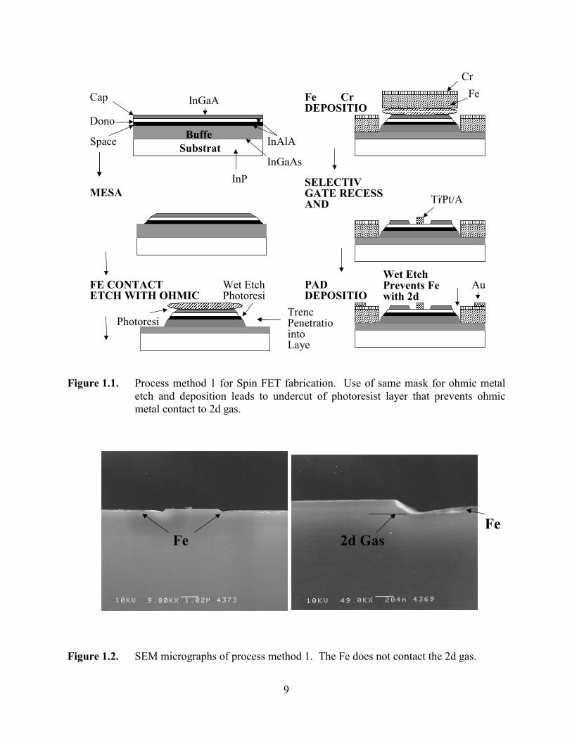
To try to enhance spin injection into the 2D gas of the FET we recess etched the ohmic
contact pads, using the ohmic mask set (process method 1). However, even though the total etch
depth was less than 1000 Å, the lateral undercut of the mask during wet etching forbid ohmic
metal contact to the 2d gas or doped cap layer or donor layer. Process method 1 is shown in
Figure 1.1. The gap in metal deposition was verified by SEM micrographs shown in Figure 1.2
and by source drain current voltage characteristics shown in Figure 1.4.
To promote ohmic contact, the next set of samples had separate levels for ohmic etch and
ohmic metal deposition (process method 2). The ohmic contact level overlapped the ohmic etch
level by ~2 µm. This forced the ohmic metal to contact the 2d gas donor and cap layer. Process
method 2 is shown in Figure 1.3. This result is verified by a much larger total current flow
shown in Figure 1.4.

8
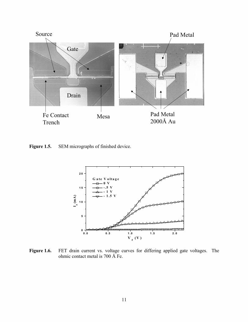
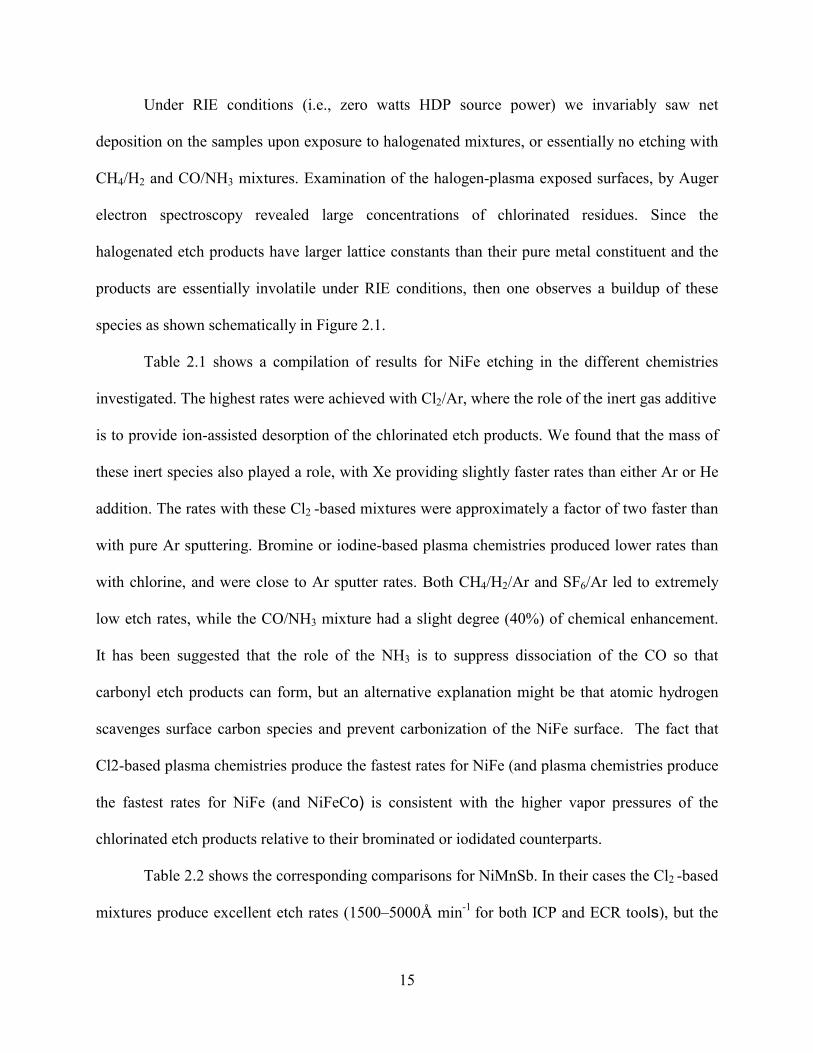
The finished devices using this process method are shown below in Figure 1.5. The
finished devices were 120 µm wide with a 1.5 µm gate. The resultant Ids gate modulated curve
is shown in Figure1.6.
In Figure 1.6 it is seen that there is ~.5 v offset voltage before the onset of current flow.
This is interesting, because it is expected that most of the current will be injected through the
highly doped cap layer; which was ohmic to the Fe contacts. The TLM measurements made to
the Fe contacted to the cap layer indicated an ohmic contact resistance of 5.2 10-5 ohm-cm2. It
may be that the rectifying characteristics of the contact are due to etch of the cap layer beneath
the contact during the rapid etching of the selective gate etch, or oxidation of the ohmic contact.
It may not be desirable to inject spins through the cap layer due to spin scattering events
caused by ionized impurity scattering and interfaces. By modifying the separate ohmic etch and
ohmic metal deposition steps, we can now test several spin injection geometries with a single
mask set that has the extra ohmic etch level. These methods are outlined in Figure 1.7.
Future Fe based contacts should have a thick layer of Au (or oxygen diffusion barrier)
deposited immediately after Fe deposition. Since Fe based contacts have been shown to be
poor spin injectors, these process methods may be best applied to dilute magnetic
semiconductor regrowth in the contact region. The same mask should be useful for both
metal contact and dilute magnetic semiconductor contacts. Careful mask design will allow
testing of several injection geometries with the inclusion of only one extra mask level; the
ohmic etch mask level. This extra ohmic etch level allows plasma etching (and therefore
damage) to be eliminated from the device processing. It also eliminates undercut of the
photoresist during etching that might inhibit contact formation.
9
MESA
FE CONTACTETCH WITH OHMIC
Fe CrDEPOSITIO
SELECTIVGATE RECESSAND Ti/Pt/A
TrencPenetratiointoLaye
PADDEPOSITIO
Wet EtchPhotoresi
Wet EtchPrevents Fewith 2d
CrFe
Au
Photoresi
Cap
Dono
Space BuffeSubstrat
InGaA
InAlA
InGaAsInP
Figure 1.1. Process method 1 for Spin FET fabrication. Use of same mask for ohmic metal
etch and deposition leads to undercut of photoresist layer that prevents ohmic metal contact to 2d gas.
FeFe
2d Gas
Figure 1.2. SEM micrographs of process method 1. The Fe does not contact the 2d gas.

10
Cap
Donor
SpacerBuffer
Substrate
MESA ISOLATION
FE CONTACT TRENCHETCH WITH PAD METALMASK
Fe AND Cr DEPOSITIONWITH OHMICMASK
SELECTIVEGATE RECESS ETCH AND DEPOSITION
Ti/Pt/Au
TrenchPenetrationinto BufferLayer
InGaAs
InAlAs
InGaAs
InP
PAD METAL DEPOSITION
Wet Etch UndercutsPhotoresist
2d Gas NowContacted by Fe
Cr
Fe
Au
Photoresist
Figure 1.3. Process method 2, for spin FET fabrication. The use of separate ohmic etch and
ohmic metal deposition masks allows ohmic metal to contact 2d gas layer.
0 .0 0 .5 1 .0 1 .5 2 .0 2 .5 3 .0 3 .50
1
2
3
4
5
P r o c e s s M e th o d 1 P r o c e s s M e th o d 2
I ds (m
A)
V d s ( V )
Figure 1.4. Comparison of source drain current between process method 1 and process
method 2.
11
Source
Drain
Gate
Pad Metal2000Å Au
Pad Metal
MesaFe ContactTrench
Figure 1.5. SEM micrographs of finished device.
0 .0 0 .5 1 .0 1 .5 2 .00
5
1 0
1 5
2 0
G a t e V o l t a g e 0 V - .5 V - 1 V - 1 .5 V
I d (mA
)
V d ( V )
Figure 1.6. FET drain current vs. voltage curves for differing applied gate voltages. The
ohmic contact metal is 700 Å Fe.

12
BufferSubstrate
Cap
Donor
Spacer
CrFe
Figure 17. Top left, no ohmic etch level, ohmic mask used for selective etch and metal deposition. Top right, Ohmic etch level used to etch to buffer layer, ohmic mask metal level used to deposit metal. Bottom, ohmic metal used to selectively etch cap layer, ohmic etch level used to etch to buffer layer, ohmic metal level repatterned to deposit metal.

13
2. Development of Chemically Assisted Dry Etching Methods for Magnetic Device Structures
(S.J. Pearton and F. Sharifi)
The push to continually increase bit densities in magnetic storage devices places
emphasis on techniques for patterning submicron metallic multilayer structures. The component
materials within these multilayers may include NiFe, NiFeCo [both are used for structures based
on the giant magnetoresistance (GMR) effect], NiMnSb (a Heusler alloy potentially useful in
advanced spin-valve structures) or the col-lossal magnetoresistance (CMR) materials
LaCaMnO3, LaSrMnO3, and PrBaCaMnO3. A general problem when processing magneto-
resistive materials is their relative invola-tility in conventional dry etching techniques such as
reactive ion etching (RIE).
Practical etch rates may be achieved under high-density plasma (HDP) conditions, where
the high ion flux is able to promote desorption of halogenated etch products. Both inductively
coupled plasma (ICP) and electron cyclotron resonance (ECR) systems have proven capable of
providing the necessary ion-to-reactive-neutral ratio (>0.02). We have completed an
examination of the etch rates of the three basic classes of materials (i.e., NiFe, NiMnSb, and the
perovskite-based CMR materials) in different plasma chemistries and also measured the long-
term magnetic and structural stability of dry etched magnetic multilayer stacks. In the latter case,
we used magnetic random access memory (MRAM) elements as our test vehicle.
The NiFe and NiMnSb layers were deposited on Si (100) substrates by direct current
magnetron sputtering from composite targets. Typical layer thicknesses were 5000Å. Liquid
delivery metalorganic chemical vapor deposition using 2,2,6,6-tetramethyl-3, 5-hepanedionato
(TMHD) precursors [i.e., La(TMHD)3 ,Sr(TMHD)2 ,Mn(TMHD)3 , and Ca(TMHD)2] was
employed to deposit films of La0.41 Ca0.59 MnO3 on Al2 O3 (0001) single crystal substrates at

14
700°C. The precursors were transported by N2 carrier gas, with direct injection of O2 and N2O as
oxidants. Films of Pr0.65 Ba0.05Ca0.3MnO3 were deposited on Si (100) in a pulsed laser ablation
system (248 nm KeF laser, 10 kHz, 2.5 J cm-2) energy density) at a substrate temperature of
700°C and an O2 partial pressure of 250 mTorr. All of the CMR films were in the range 1500–
2500Å thick.
Finally, the MRAM structures consisted of the following layers deposited on 300Å of
SiNx on 8500Å of SiO2 on Si: 80Å NiFeCo, 15Å CoFe, 35Å Cu, 15Å CoFe, 80Å NiFeCo, 200Å
Ta, 550Å TaN, and 800Å CrSi. The deposition was performed by Ar 1 ion-assisted sputtering. A
3000-Å-thick SiO2 mask was patterned by SF6/Ar RIE as the etch mask for subsequent high-
density plasma patterning of the metal layers.
The etching was performed in either Plasma-Therm 790 ICP or Plasma-Therm SLR 770
ECR reactors. In both systems the samples were thermally bonded to a radio frequency powered
(13.56 MHz) chuck which was He-backside cooled. The respective HDP sources were powered
up to 1000 W at either 2 MHz (ICP) or 2.45 GHz (ECR). The gases were injected directly into
the sources through electronic mass flow controllers at a typical load of 15–20 standard cubic
centimeters per minute. We investigated halogen- (Cl2, BI3, BBr3, ICl, IBr, SF6), CH4/H2- and
CO/NH3-based mixtures since these cover the full range of possible etch products (i.e., metal
chlorides, bromides, iodides or fluorides; metalorganics or carbonyls).
Magnetic properties before and after plasma etching were determined using
superconducting quantum interference device magnetometry (Quantum Design MPMS-5S00) at
4.2 K. Scanning electron microscopy (SEM) was used to examine sidewall smoothness on
etched features.
15
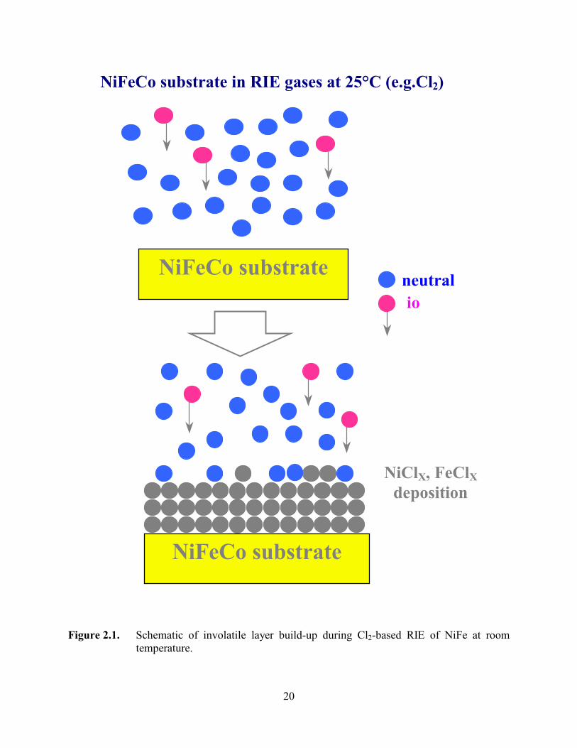
Under RIE conditions (i.e., zero watts HDP source power) we invariably saw net
deposition on the samples upon exposure to halogenated mixtures, or essentially no etching with
CH4/H2 and CO/NH3 mixtures. Examination of the halogen-plasma exposed surfaces, by Auger
electron spectroscopy revealed large concentrations of chlorinated residues. Since the
halogenated etch products have larger lattice constants than their pure metal constituent and the
products are essentially involatile under RIE conditions, then one observes a buildup of these
species as shown schematically in Figure 2.1.
Table 2.1 shows a compilation of results for NiFe etching in the different chemistries
investigated. The highest rates were achieved with Cl2/Ar, where the role of the inert gas additive
is to provide ion-assisted desorption of the chlorinated etch products. We found that the mass of
these inert species also played a role, with Xe providing slightly faster rates than either Ar or He
addition. The rates with these Cl2 -based mixtures were approximately a factor of two faster than
with pure Ar sputtering. Bromine or iodine-based plasma chemistries produced lower rates than
with chlorine, and were close to Ar sputter rates. Both CH4/H2/Ar and SF6/Ar led to extremely
low etch rates, while the CO/NH3 mixture had a slight degree (40%) of chemical enhancement.
It has been suggested that the role of the NH3 is to suppress dissociation of the CO so that
carbonyl etch products can form, but an alternative explanation might be that atomic hydrogen
scavenges surface carbon species and prevent carbonization of the NiFe surface. The fact that
Cl2-based plasma chemistries produce the fastest rates for NiFe (and plasma chemistries produce
the fastest rates for NiFe (and NiFeCo) is consistent with the higher vapor pressures of the
chlorinated etch products relative to their brominated or iodidated counterparts.
Table 2.2 shows the corresponding comparisons for NiMnSb. In their cases the Cl2 -based
mixtures produce excellent etch rates (1500–5000Å min-1 for both ICP and ECR tools), but the

16
fastest rates were achieved with SF6 /Ar mixtures. By sharp contrast, NF3 /Ar showed net
deposition rather than etching for source powers >100 W or at high NF3 percentages. The surface
under these conditions showed strong Mn enrichment and were oxidized, with an underlying Sb-
deficient region. With all of the plasma chemistries, careful attention had to be paid to the
removal of the native oxide prior to the commencement of etching to avoid the presence of a
relatively long incubation time.
For the CMR materials, we did not observe any chemical enhancement in etch rate with
any of the plasma chemistries discussed (Table 2.3). The etching was dominated by physical
sputtering under all conditions investigated, with etch yields typically <0.1 and relatively high
ion energies (>150 eV) needed to initial removal of material.
A key issue with the use of corrosive gas mixtures for etching metallic multilayers is that
of postetch stability of the patterned structures. Severe corrosion and delamination of the films is
observed in the absence of preventive measures. We examined use of several different postetch
treatments. The first was simply rinsing the samples in deionized water immediately upon
opening the chamber (which is contained within a N2 dry box). The samples were then
thoroughly dried with filtered N2. In the other three methods, various in-situ plasma cleaning
procedures were examined. After Cl2 /Ar etching was complete, the chamber was evacuated for
15 min, and then a 30 mTorr discharge of either H2, O2 or SF6 (500 W source power, 5 W chuck
power) was used to clean the residual chlorine for 10 min prior to removal of the samples from
the reactor. In these cases, no H2 O rinsing was performed. It should be pointed out that all of
these cleaning procedures have been employed previously for removing etch residues after Cl2-
based plasma etching of Al interconnects in Si microelectronics.

17
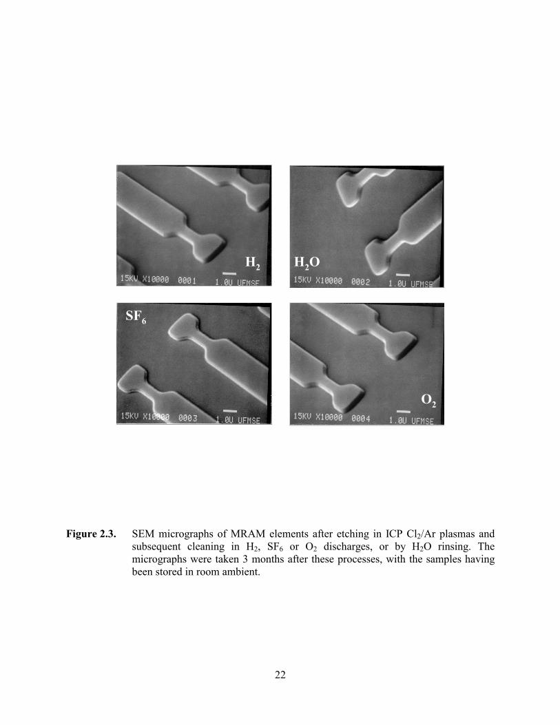
Figure 2.2 shows the magnetization of each of the samples over a period of
approximately six months. In each case the samples were simply stored in air between the
measurements and no special precautions were taken to prevent corrosion. Each of the cleaning
procedures produces samples with extremely stable magnetic characteristics. This is also
reflected in their appearance. Figure 2.3 shows SEM micrographs of patterned MRAM elements
three months after Cl2/Ar etching and postetch cleaning. There is no indication of corrosion on
any of the samples and the sidewalls are smooth (to the resolution used in the photos). There is
no indication of striations often observed on dry etched features. Note, however, that in the case
of O2 plasma cleaned samples there was a slight decrease in the magnetization per unit volume
relative to the samples treated in water or H2 or SF6 plasmas. A possible reason for this is that the
feature sidewalls become more oxidized than with other treatments, leading to a degradation in
magnetic properties.
A comprehensive survey of etching results for magnetic materials in different plasma
chemistries has produced the following conclusions:
(i) The optimum chemistry for NiFe is Cl2/Ar, for NiMnSb is SF6/Ar, while no
chemical enhancement of etch rates for CMR oxides was observed.
(ii) Postetch rinsing in H 2 O or in-situ plasma cleaning with H2, O2 or SF6 discharges
are all effective treatments for removing chlorine etch residues. Of these, only O2
plasma exposure appears to degrade the magnetic properties of MRAM stacks.
Once the residues are removed, there is no change in magnetic or visual properties
over a period of ~six months (extent of our study).
(iii) The CO/NH3 chemistry, while being noncorrosive, produces relatively slow etch
rates and is only suitable for patterning of thin (<1000Å) structures.

18
TABLE 2.1. Comparison of plasma chemistries for NiFe etching.
Chemistry
Typical Etch Rates
Corrosive
Comments
10Cl2/5Ar 600Å min-1 ICP
>1000Å min-1 ECR Yes Chemical enhancement of 100%
Etch rate with Xe>Ar>He
13CO/2NH3 250Å min-1 ICP 500Å min-1 ECR
No Chemical enhancement of ~20%–40% CO2 less effective than CO
5CH4/10H2/5Ar <100Å MIN-1 ICP, ECR No Slower than Ar sputtering 10SF6/5Ar <100Å min-1 ICP, ECR No Slower than Ar sputtering 10BI3/5Ar 500Å min-1 ICP, ECR Yes Less effective than Cl2/Ar 10BBr3/5Ar 200Å min-1 ICP, ECR Yes Slower than Ar sputtering 10ICl/5AR 500Å min-1 ICP, ECR Yes Excellent surface morphology 10IBr/5Ar 500Å min-1 ICP, ECR Yes Excellent surface morphology
Table 2.2. Comparison of plasma chemistries for NiMnSb etching.
Chemistry
Typical Etch Rates
Corrosive
Comments
10SF6/5Ar >10,000Å min-1 ICP, ECR No Selectivity ≥20 over Al2O3
10NF3/5Ar 300Å min-1 ICP, ECR No Narrow process window
10Cl2/5Ar 3,000Å min-1 ICP, ECR Yes Selectivity ≥5 over Al2O3
10BCl3/5Ar 5,000Å min-1 ICP, ECR Yes Selectivity ≥5 over Al2O3
Attacks native oxide
10ICl/5Ar 1500Å min-1 ICP, ECR Yes Threshold ion energy 120 eV
10IBr/5Ar 1500Å min-1 ICP, ECR Yes Threshold ion energy 230 eV

19
Table 2.3. Comparison of plasma chemistries for CMR etching.
Chemistry
Typical Etch Rates
Corrosive
Comments
10SF6/Ar 500Å min-1 LaCaMnO3 ICP, ECR No No chemical enhancement
5CH4/10H2/5Ar 200Å min-1 LaCaMnO3 ICP, ECR No No chemical enhancement
10Cl2/5Ar 1500Å min-1 LaCaMnO3 ICP, ECR
900Å min-1 LaSrMnO3 ICP
300Å min-1 PrBaCaMnO3 ICP
Yes Physically dominated under all conditions for all three materials
10BI3/5Ar 500Å min-1 LaCaMnO3 ICP, ECR Yes Etch yield <0.1 threshold ion energy <100 eV
10BBr3/5Ar 500Å min-1 ICP, ECR Yes Threshold ion energy ~150 eV
20
Figure 2.1. Schematic of involatile layer build-up during Cl2-based RIE of NiFe at room
temperature.
NiFeCo substrate
NiFeCo substrate in RIE gases at 25°C (e.g.Cl2)
NiFeCo substrate
NiClX, FeClXdeposition
ioneutral

21
Figure 2.2. Magnetization of MRAM structures, either unetched or etched in Cl2/Ar plasmas
and subsequently cleaned in water, or in H2, SF6 or O2 plasmas, as a function of subsequent storage time in room ambient.
0 40 80 120 1600.0
0.2
0.4
0.6 Magnetization vs. Time
H2 cleaning DI water rinsing SF6 cleaning O2 cleaning Control
M/v
ol (e
mu/
mm
3 )
Time (days)
22
Figure 2.3. SEM micrographs of MRAM elements after etching in ICP Cl2/Ar plasmas and
subsequent cleaning in H2, SF6 or O2 discharges, or by H2O rinsing. The micrographs were taken 3 months after these processes, with the samples having been stored in room ambient.
H2 H2O
SF6
O2

23
3. Effects Of UV Illumination On Dry Etch Rates Of NiFe-Based Magnetic Multilayers
(S.J. Pearton)
There is a strong interest in the development of plasma etching processes for magnetic
multilayer structures of the type used in sensors, magnetic random access memories or read/write
heads for data storage. There are two basic plasma chemistries that have been reported to etch
NiFe and NiFeCo under high ion density conditions, namely Cl2 and CO/NH3. The etch rates are
still low (< 500 Å/min) and are limited by desorption of the reaction products. Recently, several
groups have reported that ultra-violet light irradiation during Inductively Coupled Plasma (ICP)
etching of Cu in Cl2-based discharges lowered the activation energy for etching, and also
enhanced the desorption of the CuCl products. In that case, the UV light was assumed to be
absorbed by the CuCl, promoting nonthermal desorption.
In this paper we report on the effects of UV illumination on ICP etch rates of NiFe and
NiFeCo in Cl2/Ar and CO/NH3 discharges. In the latter chemistry there was no measurable
enhancement in etch rates under a wide range of plasma conditions. In the case of Cl2/Ar,
however, the UV irradiation decreased the NiFe etch rate and more chlorine residues were
detected on the NiFe surface. Only in the case of Cl2/Ar etching of NiFeCo were enhancements
in removal rate obtained with UV irradiation.
The Ni0.8Fe0.2 and Ni0.8Fe0.13Co0.07 layers were deposited on Si(100) substrates by dc
magnetron sputtering from composite targets. Typical layer thicknesses were 5000 Å. Some of
the samples were masked with Apiezon wax for etch rate measurements. The etch depths were
measured by stylus profilometry after removal of the mask in acetone. The morphology and
composition of unmasked samples was examined by Atomic Force Microscopy (AFM) and
Auger Electron Spectroscopy (AES), respectively.

24
The etching was performed in a Plasma-Therm 790 ICP reactor, with the samples
thermally bonded to a rf powered (13.56 MHz) He backside-cooled chuck. The gases were
injected directly into the ICP source (2 MHz, 1000 W) through electronic mass flow controllers
at a total load of 15 standard cubic centimeters per minute (sccm). An unfiltered 400 W Hg arc
lamp was installed on top a 1 inch diameter quartz window on top of the ICP source (~ 20 cm
from the sample position) and provided illumination of the samples during plasma etching. We
believe any sample heating due to the lamp is minimal (< 10 oC) because the samples were
thermally bonded to a Si carrier wafer and the resist mask showed no evidence of thermal
degradation or flow.
Table 3.1 shows thermochemical data for the potential metal chloride or metal carbonyl
etch products for NiFe and NiFeCo in Cl2 or CO/NH3 plasmas. From this data we can calculate
the Gibbs free energies of reactions of Ni, Fe and Co with atomic or molecular chlorine, and with
CO and CO2. There are several important features of this data in Table 3.2. First, the reaction of
the metals is more favorable with atomic chlorine than with Cl2, which emphasizes the need for
efficient dissociation of the feedstock gas in the plasma source. Second, CO is more reactive
with the metals than is CO2, as we have previously reported in a comparison of the two gases.
We emphasize that in a plasma etching environment there will be a strong ion-assisted
component to the etch mechanism and the thermodynamic data provides only a guide to the
reaction pathways.
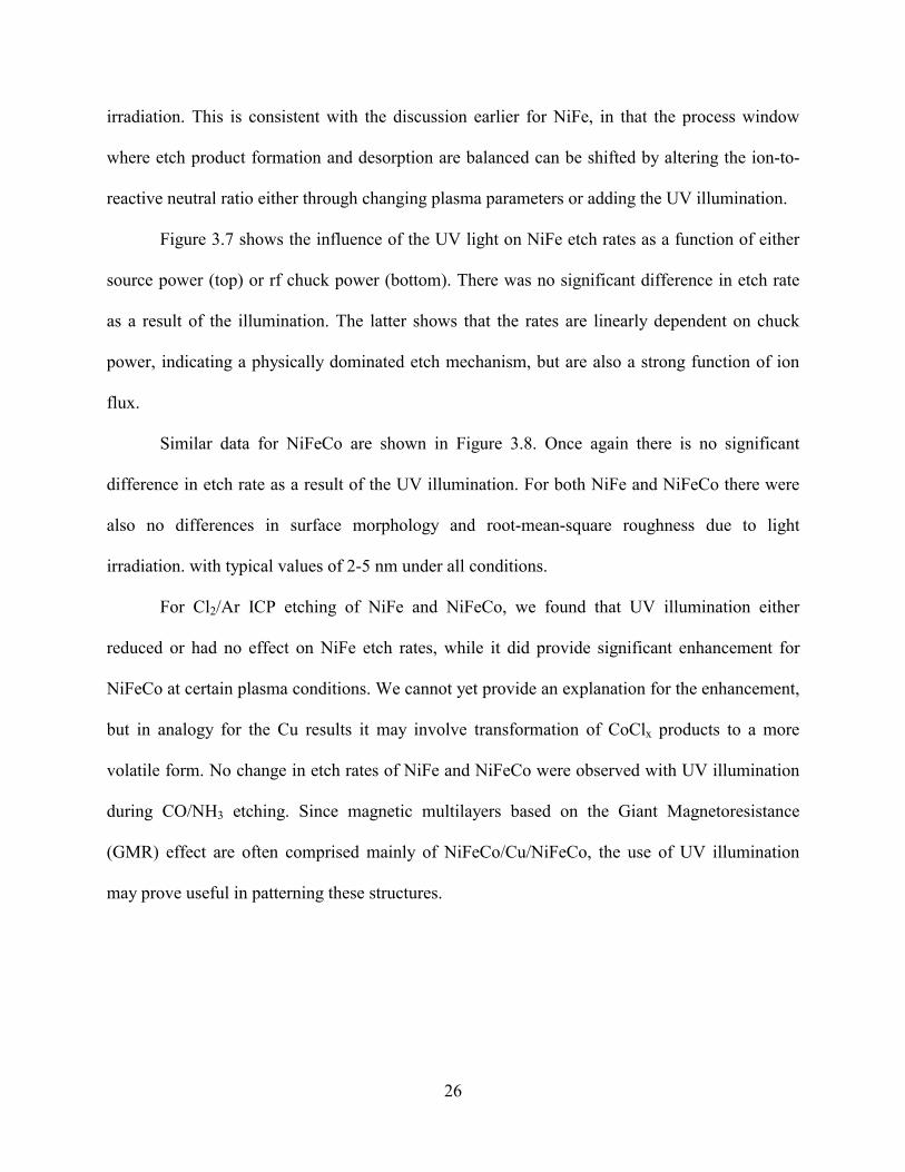
Figure 3.1 shows the effect of source power (top) and rf chuck power (bottom) in NiFe
etch rates in 10Cl2/5Ar discharges at fixed process pressure (2 mTorr). The source power
controls ion flux and efficiency of plasma dissociation, while the chuck power controls the

25
average ion energy. Note that at this plasma composition the use of UV illumination actually
retards the etching and in fact promotes net deposition on the sample.
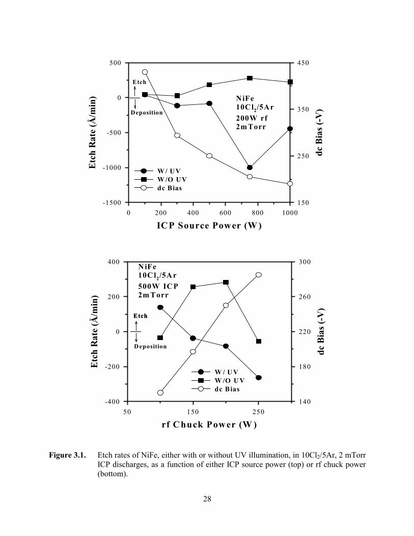
Examination of the samples etched either with or without UV illumination by AES
showed more chlorine-related residues in the former case. Figure 3.2 shows AES surface scans
of samples etched in 10Cl2/5Ar discharges at either 500 W source power, 100 W rf chuck power
(top, left and right) or 750 W source power, 200 W rf chuck power (bottom, left and right). The
samples etched without UV illumination (top and bottom right) have much smaller Cl signals on
their surfaces. The effect of the UV in this case is clearly to enhance formation of FeClx and
NiClx species on the surface, but not to enhance their desorption. We have previously found that
a process window exists for Cl2/Ar etching of NiFe in which the formation of the chloride
reaction products must be balanced with their ion-assisted desorption.
The fact that the UV illumination alters their process window is evident from the data in
Figure 3.3. At a lower Cl2 concentration in the discharge (5Cl2/10Ar), the etch rate is now
positive (i.e., no deposition) for all source and chuck powers. However, there are still no
conditions where the UV provides an enhancement in etch rate. Moreover, the etched surface
morphologies were not improved by UV illumination, as shown in the AFM scans of Figure 3.4.
By sharp contrast to the results for NiFe, we did observe significant etch rate
enhancements for NiFeCo with UV irradiation. Figure 3.5 shows the effect of source power (top)
and of chuck power (bottom) on NiFeCo etch rates in 10Cl2/5Ar discharges, either with or
without UV illumination. We obtained a maximum enhancement of approximately a factor of 3
at relatively high source powers or chuck powers.
Figure 3.6 shows similar results for NiFeCo etching at lower Cl2 concentration in the
discharge (5Cl2/10Ar). In this case there was no measurable change in etch rate with UV
26
irradiation. This is consistent with the discussion earlier for NiFe, in that the process window
where etch product formation and desorption are balanced can be shifted by altering the ion-to-
reactive neutral ratio either through changing plasma parameters or adding the UV illumination.
Figure 3.7 shows the influence of the UV light on NiFe etch rates as a function of either
source power (top) or rf chuck power (bottom). There was no significant difference in etch rate
as a result of the illumination. The latter shows that the rates are linearly dependent on chuck
power, indicating a physically dominated etch mechanism, but are also a strong function of ion
flux.
Similar data for NiFeCo are shown in Figure 3.8. Once again there is no significant
difference in etch rate as a result of the UV illumination. For both NiFe and NiFeCo there were
also no differences in surface morphology and root-mean-square roughness due to light
irradiation. with typical values of 2-5 nm under all conditions.
For Cl2/Ar ICP etching of NiFe and NiFeCo, we found that UV illumination either
reduced or had no effect on NiFe etch rates, while it did provide significant enhancement for
NiFeCo at certain plasma conditions. We cannot yet provide an explanation for the enhancement,
but in analogy for the Cu results it may involve transformation of CoClx products to a more
volatile form. No change in etch rates of NiFe and NiFeCo were observed with UV illumination
during CO/NH3 etching. Since magnetic multilayers based on the Giant Magnetoresistance
(GMR) effect are often comprised mainly of NiFeCo/Cu/NiFeCo, the use of UV illumination
may prove useful in patterning these structures.

27
Table 3.1. Thermochemical data for potential etch products (Ref. 11).
Species
∆∆∆∆H0
f.298 K(kJ/mol)
S0298 K (J/mol K)
∆∆∆∆G0
f.298 K (kJ/mol)a
FeCl2 (s) -341.833 117.947 -302.342
FeCl3 (s) -399.405 142.336 -333.930
CoCl2 (s) -312.545 109.266 -269.647
NiCl2 (s) -304.930 98.157 -258.779
Fe(CO)5 (s) -766.090 337.078 -696.975
Fe(CO)5 (s) -727.849 439.286 -389.207
Ni(CO)4 (s) -631.784 319.560 -588.980
Ni(CO)4 (s) -601.576 415.507 -587.378
Co(CO)4 (s) -562.100 -337.442 -535.024
Table 3.2. Thermodynamic data for possible etch reactions.
Fe(s) + 2Cl(g)↔FeCl2(s) ∆G0r = -512.9 (kJ/mol)
Fe(s) + Cl2(g)↔FeCl2(s) ∆G0r = -302.3 (kJ/mol)
Fe(s) + 5CO(g) ↔Fe(CO)5 (1) ∆G0r = -11.2 (kJ/mol)
↔Fe(CO)5 (g) ∆G0r = -3.4 (kJ/mol)
Fe(s) + 5CO2(g) ↔Fe(CO)5(1)+2.502(g) ∆G0r = 1274.9 (kJ/mol)
↔Fe(CO)5(g)+2.502(g) ∆G0r = 1282.7 (kJ/mol)
Ni(s)+2Cl(g)↔NiCl2(s) ∆G0r = -359.4 (kJ/mol)
Ni(s)+Cl2(g)↔NiCl2(s) ∆G0r = -258.8 (kJ/mol)
Ni(s)+4CO(g)↔Ni(CO)4 (1) ∆G0r = -40.3 (kJ/mol)
↔Ni(CO)4(g) ∆G0r = -38.7 (kJ/mol)
Ni(s)+4CO2(g)↔Ni(CO)4(1)+2O2(g) ∆G0r = 988.6 (kJ/mol)
↔Ni(CO)4(g)+2O2(g) ∆G0r = 990.2 (kJ/mol)
Co(s)+2Cl(g)↔CoCl2(s) ∆G0r = -380.3 (kJ/mol)
Co(s)+Cl2(g)↔CoCl2(s) ∆G0r = -269.6 (kJ/mol)
Co(s)+4CO(g)↔Co(CO)4(g) ∆G0r = 13.6 (kJ/mol)
Co(s)+4CO2(g)↔Co(CO)4(1)+202(g) ∆G0r = 1042.5 (kJ/mol)
28
Figure 3.1. Etch rates of NiFe, either with or without UV illumination, in 10Cl2/5Ar, 2 mTorr
ICP discharges, as a function of either ICP source power (top) or rf chuck power (bottom).
ICP Source Power (W )0 200 400 600 800 1000
Etc
h R
ate
(Å/m
in)
-1500
-1000
-500
0
500
dc B
ias (
-V)
150
250
350
450
W / UVW /O UVdc Bias
NiFe10Cl2/5Ar200W rf2m Torr
Etch
Deposition
rf Chuck Power (W )50 150 250
Etc
h R
ate
(Å/m
in)
-400
-200
0
200
400
dc B
ias (
-V)
140
180
220
260
300
W / U VW /O U Vdc Bias
N iFe10C l2/5A r500W IC P2m Torr
EtchEtch
D eposition
29
Figure 3.2. A
ES surface scans of NiFe (top) or N
iFeCo (bottom
) after etching in 10Cl2 /5A
r, 2 m
Torr discharges, either with (tip and bottom
left) or without (top and bottom
right) U
V illum
ination under conditions of 500 W source pow
er, 100 W rf chuck
power (top, left and right) or 750 W
source power, 200 W
rf chuck power
(bottom, left and right).
10 86420
N(E)/E
400800
12001600
2000K
INETIC
ENER
GY
, eV
400800
12001600
2000K
INETIC
ENER
GY
, eV
1086420
N(E)/E
NiFe
500W IC
P 100W
rf W
/ UV
NiFe
500W IC
P 100W
rf W
/O U
V
Cl
Cl
O
O
CC
Ni
Ni
Fe Fe
4080
120160
200K
INETIC
ENER
GY
, eV
10 86420
N(E)/E
1086420N(E)/E
NiFeC
o 750W
ICP
200W rf
W/ U
V
Cl
O
C
Ni
Fe
400800
12001600
2000 K
INETIC
ENER
GY
, eV
NiFeC
o 750W
ICP
200W rf
W/O
UV
Cl
O
C
Ni
Fe

30
Figure 3.3 Etch rates of NiFe, either or without UV illumination, in 5Cl2/10Ar, 2 mTorr ICP discharges, as a function of either ICP source power (top) or rf chuck power (bottom).
ICP Source Power (W)0 200 400 600 800 1000
Etch
Rat
e (Å
/min
)
0
200
400
600
dc B
ias (
-V)
200
300
400
150
250
350
W/ UVW/O UVdc Bias
NiFe5Cl2/10Ar200W rf2mTorr
rf Chuck Power (W)100 200 30050 150 250
Etc
h R
ate
(Å/m
in)
0
200
400
600
800
dc B
ias (
-V)
120
160
200
240
280
W/ UVW/O UVdc Bias
NiFe5Cl2/10Ar500W ICP2mTorr

31
Figure 3.4 AFM scans of NiFe after etching in 5Cl2/10Ar, 500 W source power discharges,
either with or without UV illumination, at different rf chuck powers.
4 8 µm
4 8 µm
4 8 µm
4 8 µm
4 8 µm
4 8 µm
W/O UV W/ UV
100W rf
250W rf
200W rf
RMS: 2.883 nm RMS: 5.415 nm
RMS: 5.195 nm RMS: 6.043 nm
RMS: 9.031 nm RMS: 6.973 nm

32
Figure 3.5 Etch rates of NiFeCo, either or without UV illumination, in 10Cl2/5Ar, 2 mTorr
ICP discharges, as a function of either ICP source power (top) or rf chuck power (bottom).
ICP Source Power (W )0 200 400 600 800 1000
Etch
Rat
e (Å
/min
)
0
400
800
1200
dc B
ias (
-V)
150
250
350
450
W / UVW /O UVdc Bias
Etch
Deposition
NiFeCo10Cl2/5Ar200W rf2mTorr
rf Chuck Power (W )50 150 250
Etc
h R
ate
(Å/m
in)
0
200
400
600
800
dc B
ias (
-V)
100
200
300
W / UVW /O UVdc Bias
NiFeCo10Cl2/5Ar500W ICP2mTorr

33
Figure 3.6 Etch rates of NiFeCo, either or without UV illumination, in 5Cl2/10Ar, 2 mTorr
ICP discharges, as a function of either ICP source power (top) or rf chuck power (bottom).
ICP Source Power (W )0 200 400 600 800 1000
Etc
h R
ate
(Å/m
in)
0
200
400
600
800
dc B
ias (
-V)
200
300
400
150
250
350
W / UVW /O UVdc Bias
NiFeCo5Cl2/10Ar200W rf2mTorr
rf Chuck Power (W)100 200 30050 150 250
Etch
Rat
e (Å
/min
)
-200
0
200
400
600
800
dc B
ias (
-V)
120
160
200
240
280
W/ UVW/O UVdc Bias
NiFeCo5Cl2/10Ar500W ICP2mTorr
Etch
Deposition

34
Figure 3.7. Etch rates of NiFe, either or without UV illumination, in 10CO/5NH3, 2 mTorr
ICP discharges, as a function of either ICP source power (top) or rf chuck power (bottom).
ICP Source Power (W )0 200 400 600 800 1000
Etc
h R
ate
(Å/m
in)
0
100
200
300
400
dc B
ias (
-V)
250
350
200
300
400
W / U VW /O UVdc Bias
NiFe10CO /5NH 3
200W rf2m Torr
rf Chuck Power (W )100 200 30050 150 250
Etc
h R
ate
(Å/m
in)
0
100
200
300
dc B
ias (
-V)
200
300
400
150
250
350
W / UVW /O UVdc Bias
NiFe10CO/5NH 3
500W ICP2mTorr

35
Figure 3.8. Etch rates of NiFeCo, Either with or without UV illumination, in 10CO/5NH3, 2
mTorr ICP discharges, as a function of either ICP source power (top) or rf chuck power (bottom).
ICP Source Power (W)0 200 400 600 800 1000
Etc
h R
ate
(Å/m
in)
0
100
200
300
400
dc B
ias (
-V)
250
350
200
300
400
W/ UVW/O UVdc Bias
NiFeCo10CO/5NH3
200W rf2mTorr
rf Chuck Power (W )100 200 30050 150 250
Etc
h R
ate
(Å/m
in)
150
250
100
200
dc B
ias (
-V)
200
300
400
150
250
350
W / UVW /O UVdc Bias
NiFeCo10CO/5NH 3
500W ICP2mTorr

36
4. Dry Etching Mechanism Of Copper And Magnetic Materials With UV Illumination (S.J. Pearton)
In recent years several research groups have studied dry etching of copper for the next
generation of metallization in the semiconductor industry, focusing on development of new etch
techniques to increase etch rate. They used Cl2 plasmas with or without photon sources using
ultraviolet (UV) laser, UV lamp, illumination and IR light. In contrast to conventional dry
etching that requires relatively high temperatures (> 200oC) in order to produce practical etch
rates, they all reported substantial enhancement of etch rates at low temperatures. Among them
Choi and Han first reported high etch rates of about 3000 Å/min at room temperature with Cl2
discharges in an Inductively Coupled Plasma (ICP) system.
Magnetic materials such as NiFe and NiFeCo are widely used in sensors, magnetic
random access memories (MRAMs) or read/write heads for data storage industry. Due to the
relative inertness of these materials there is a strong interest in the development of high density
plasma etching processes for them. There are two basic plasma chemistries for the etching of
NiFe and NiFeCo under ICP conditions, namely Cl2 and CO/NH3. However, the etch rates are
still low (< 500 Å/min) and are limited by desorption of the etch products such as NiClx, FeClx
and CoClx. Cho et al. first reported the effect of UV illumination on the etch rates of the NiFe-
based magnetic materials
Since the etch mechanism with UV illumination has not been studied in detail, in this
paper we propose an etch mechanism of copper and magnetic materials with UV irradiation
based on subprocesses occurring in the Cl2 -ICP etching system. We also carried out ICP etching
of NiFe and NiFeCo in Cl2/Ar discharges with or without UV illumination. We found that the
chlorination of copper surface is enhanced with UV irradiation and the absorption of UV photons
by metal chlorides is critical to enhance the removal rate of chlorides. The proposed etch

37
mechanism of copper showed good agreement with observed data determined by mass
spectrometry, taken from the literature.
4.1. Etch Mechanism of ICP Etching of Cu with UV Illumination
There are likely five subprocesses involved in etching of copper with UV illumination: 1)
photo-dissociation of Cl2 in gas phase, 2) surface chlorination, 3) absorption of UV photons by
reaction products, 4) photo-assisted removal of reaction products, and 5) Gas-phase reactions
between desorbed species.
(a) Photo-dissociation of Cl2
In addition to formation of Cl radicals by electron-collision in the bulk plasma, more Cl2
molecules are dissociated by collision between photons and molecules:
Cl2 + hν → 2Cl (1)
The above reaction is readily occurred because the bond strength of Cl2 is 2.5 eV and the UV
photon energies are 2 - 4 eV. Hence, compared to the plasmas without UV illumination, the
photo-dissociation reaction provides chlorine-enriched environment, and the reactive chlorine
radicals easily take part in surface reactions.
(b) Surface chlorination
When the copper surface is exposed to UV radiation, electrons are ejected by photo-
electron effect and are captured by chlorine radicals near the surface, leading to chlorination of
the copper surface:
Cu(s) + hν → Cu+ + e (2)
xCl(g) + e → xCl-(g) (3)
Cu(s) + xCl(g) → CuClx(s), ∆Gor = - 226 (kJ/mol) (4)

38
In contrast to dry etching without UV illumination, UV photons promote the chemistry at the
copper surface, resulting in fast deposition of metal chlorides on the surface with low activation
energy. This chlorination reaction is induced by photons and the reaction rate is thus a strong
function of photon flux or UV intensity. Since the unreacted Cu surface absorbs UV photons and
is readily chlorinated by the above reaction, most sites of the copper surface will be chlorinated,
leading to the formation of stoichiometric copper chloride.
Under chlorine-enriched conditions, copper chloride may further react with chlorine
radicals to form CuCl2(s):
CuCl(s) + Cl(g) → CuCl2(s), ∆Gor = - 146 (kJ/mol) (5)
The chlorination reactions of (4) and (5) may produce the copper chlorides having the Cl content
equal to or greater than stoichiometric ratio, i.e. x ≥ 1. If there are no UV photons involved, the
Cl concentration will be strongly dependent on reaction time. The surface chlorination also
weakens Cu-Cu bond strength, resulting in lowering etch threshold.
(c) Absorption of UV radiation by reaction products
The enhancement of etch rate with UV illumination indicates that the UV photons play an
important role in etching mechanism. The clue to this suggestion is the optical properties of the
reaction products, CuClx. Tables 4.1 and 4.2 show the optical constants of some materials
available in terms of reflectivity (Table 4.1) and adsorption depth (Table 4.2). Compared to
metal copper, CuCl has much smaller reflectivity (or longer adsorption depth). This indicates
copper chloride absorbs most UV photon energies, and in turn the photons excite electrons of the
reaction products so that the bond strength becomes weaker. This phenomenon may play a key
role in increasing the etch rates of copper. If a metal chloride has a low absorption capacity of
UV light, the effect of UV illumination will be less significant. Hence, the overall etch process of

39
metals with UV illumination is limited by absorption of UV radiation, which is determined by
optical properties of the metal chlorides.
(d) Photo-assisted removal of metal chlorides at the surface
As soon as the copper chlorides are formed, they absorb UV radiation, resulting in
excitation of valence-electrons in the CuClx layer, weakening bond strengths of CuClx and
CuClx-Cu. This could lead to rupture of surface bonds and subsequent desorption. It is
noteworthy that CuCl has a direct bandgap of 3.26 eV at 300 K. The UV photon energies in the
range 2-4 eV can also be utilized to sublime the copper chloride [1.6 eV for Cu3Cl3(g) and 2.2
eV for CuCl(g)]. Hence, the possible photo-assisted removal process of the chlorinated surface
can be described as:
CuCl(s) + hν → Cu(g) + Cl(g) (6)
3CuCl(s) + hν → Cu3Cl3(g) (7)
CuCl(s) + hν → CuCl(g) (8)
Cu(s) + hν → Cu(g) (9)
Photon-sputtering represented by Eq. (9) could be occurring on the unchlorinated or etched
surface due to lower bond energy of Cu-Cu (1.83 eV) than UV photon energies.
The photon-assisted etch reactions of (6)-(9) are greatly affected by UV intensity because
they do not occur without formation of copper chloride and the formation rate is a function of
photon flux, implicating a higher etch rate with higher UV intensity.
(e) Gas-phase reactions between desorbed species
Some of the desorbed molecules tend to capture electrons and form negative ions, and
react with reactive radicals such as Cl and Cu. There are many possible reactions among
desorbed species, radicals and ions in gas phase. They can be summarized as:
40
CuCl(g) + e → CuCl-(g) (10)
CuCl2(g) + e → CuCl2-(g) (11)
CuCl (g) + Cl(g) → CuCl2 (g) (12)
CuCl-(g) + Cl(g) → CuCl2(g) + e (13)
CuCl (g) + Cu(g) → Cu2Cl(g) (14)
CuCl2-(g) + Cu(g) → Cu2Cl2(g) + e (15)
CuCl2-(g) + Cu(g) + Cl(g) → Cu2Cl3(g) + e (16)
CuCl2-(g) + Cu(g) + Cl(g) → Cu2Cl3(g) (17)
Cu2Cl2(g) + Cl(g) → Cu2Cl3(g) (18)
Cu2Cl2(g) + Cu(g) → Cu3Cl2(g) (19)
Cu2Cl3(g) + Cu(g) → Cu3Cl3(g) (20)
The gas-phase reactions under plasma and UV illumination conditions indicate that the most
favored forms of product gas are CuCl2 (Eqs. (11) - (13)) and Cu2Cl3 (Eqs. (16)-(18)). This may
be confirmed with examining the relative peak intensities of the observed mass distributions of
species using mass spectrometry. Although we may consider photo-assisted dissociation of
CuCl(g) and Cu3Cl3(g), it seems unlikely due to the high bond energy of Cu-Cl, 3.97 eV. The
ionization energies of copper chlorides are also quite high: 10.7 eV for CuCl+, 9.6 eV for
Cu2Cl2+, and 9.7 eV for Cu3Cl3
+. Hence the ionization of copper chloride gases does not occur
under the UV illumination conditions.
4.2. Etch Mechanism of Magnetic Materials with UV Illumination
Successful etching of NiFe and NiFeCo with Cl2 plasmas has been reported. However, due to
the relative involatility of the etch products such as NiClx, FeClx and CoClx the attainable etch

41
rates are quite low (≤ 500 Å/min). The etch rates of these materials in a high density plasma
reactor are function of ion flux, ion energy and plasma composition. To examine the effect of
UV illumination on etch rate we have to know the optical properties of the magnetic materials
and reaction products. However, their optical properties are not available yet. There is however,
a substantial increase in etch rate with UV illumination over etching without UV irradiation.
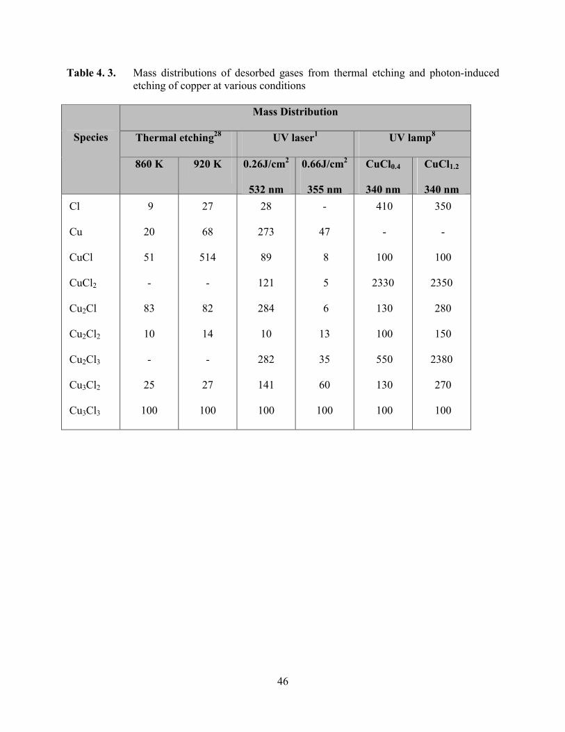
Table 4.3 summarizes the mass distributions of desorbed gaseous products observed from
thermal etching and photon-induced etching of copper. These mass distributions are normalized
to the Cu3Cl3 intensity. It is seen that for thermal desorption, the major gases are Cu3Cl3 at 860 K
and CuCl at 920 K, but no CuCl2 and Cu2Cl3 are observed. However, UV laser induced etching
showed that the dominant gas species were Cu, Cu2Cl, Cu2Cl3 and Cu3Cl2 with laser fluence of
0.26 J/cm2 per pulse with 532 nm, and Cu, Cu3Cl2 and Cu3Cl3 with 0.66 J/cm2 and 355 nm. The
observation of copper signal is attributed to photon-sputtering due to the strong laser energy. By
contrast, Kwon et al. reported CuCl2 and Cu2Cl3 as the dominant gases observed from ICP
etching of copper with UV illumination regardless of chlorine content in copper chlorides. It is
also interesting to note that the desorbed gases are Cl, CuCl, CuCl2, Cu2Cl, Cu2Cl2, Cu2Cl3,
Cu3Cl2, and Cu3Cl3 in all cases of photon-assisted etching. Furthermore, no observation of CuCl2
and Cu2Cl3 during the thermal desorption indicates that their presence in the etching with UV
illumination is not originated from cracking of Cu3Cl3 by the ionizer of the mass spectrometer. It
seems clear that CuCl2 and Cu2Cl3 are produced in the ICP etching of copper with UV
illumination. Hence, these previous results overall support the etch mechanism proposed in this
paper.
Kwon et.al. also confirmed that the copper chloride layer formed with UV illumination
had a higher chlorine content than stoichiometry (i.e. x > 1.0) regardless of reaction time, and it
42
was composed of CuCl(s) and CuCl2(s). This is contrary to the much lower chlorine content
obtained without UV illumination. However, this result is attributed to the fact that the copper
surface is easily chlorinated under UV illumination because UV photons promote the chemistry
at the surface and lower the activation energy. Choi and Han reported the activation energy of
0.12 eV, which is much lower than the energy of 1.6 eV required to sublime CuCl(s) to
Cu3Cl3(g). This confirms that the dry etching with UV illumination is not a simple thermal
desorption, but a nonthermal etch mechanism due to the presence of UV photons.
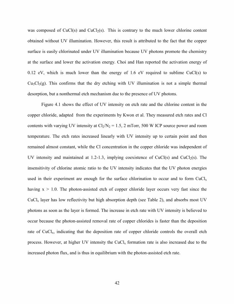
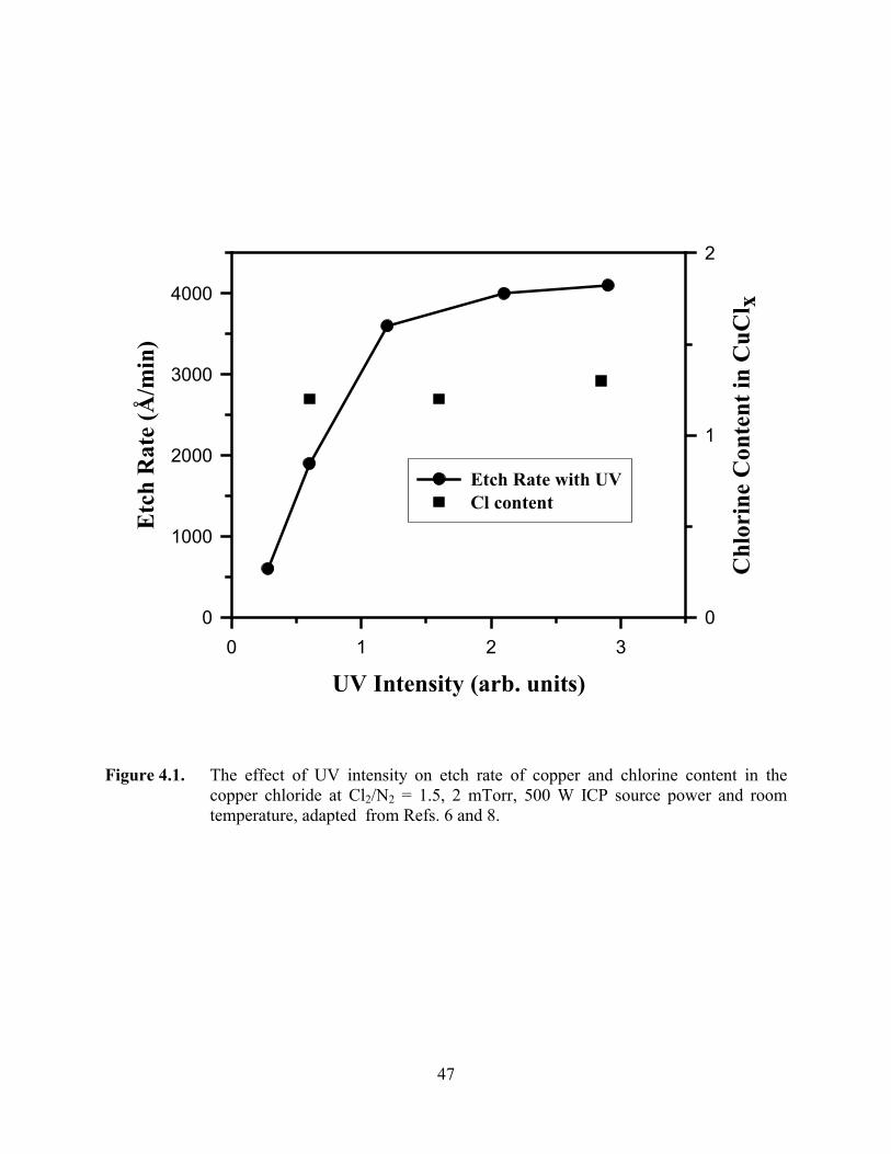
Figure 4.1 shows the effect of UV intensity on etch rate and the chlorine content in the
copper chloride, adapted from the experiments by Kwon et al. They measured etch rates and Cl
contents with varying UV intensity at Cl2/N2 = 1.5, 2 mTorr, 500 W ICP source power and room
temperature. The etch rates increased linearly with UV intensity up to certain point and then
remained almost constant, while the Cl concentration in the copper chloride was independent of
UV intensity and maintained at 1.2-1.3, implying coexistence of CuCl(s) and CuCl2(s). The
insensitivity of chlorine atomic ratio to the UV intensity indicates that the UV photon energies
used in their experiment are enough for the surface chlorination to occur and to form CuClx
having x > 1.0. The photon-assisted etch of copper chloride layer occurs very fast since the
CuClx layer has low reflectivity but high absorption depth (see Table 2), and absorbs most UV
photons as soon as the layer is formed. The increase in etch rate with UV intensity is believed to
occur because the photon-assisted removal rate of copper chlorides is faster than the deposition
rate of CuClx, indicating that the deposition rate of copper chloride controls the overall etch
process. However, at higher UV intensity the CuClx formation rate is also increased due to the
increased photon flux, and is thus in equilibrium with the photon-assisted etch rate.

43
Figure 4.2 shows the effect of ICP source power in our reactor on etch rates of Ni0.8Fe0.2
(top) and Ni0.8Fe0.13Co0.07 (bottom) with or without UV illumination in Cl2 plasmas at 10 sccm
Cl2/5 sccm Ar, 200 W rf chuck power, 2 mTorr and room temperature. In these experiments an
unfiltered 400 W Hg arc lamp was used for UV irradiation. Details of the experiment are
described elsewhere. There is net deposition observed on NiFe, indicating the rate of formation
of metal chlorides is greater than their removal rates. This result also implies that reaction
products such as NiClx and FeClx are not absorbing UV photons. The increase in the formation
rate of metal chlorides is attributed to the increased chlorine radicals with UV illumination and
the chemistry promoted at the surface by photons. In contrast to NiFe, NiFeCo showed an overall
increase in etch rate with UV illumination, especially at moderate ICP source powers (500-800
W). This may be attributed to two factors: 1) lower binding energy of NiFeCo than NiFe (for
example, see the Fe-Co phase diagram; addition of Co to Fe lowered the melting point of FeCo
alloy), and 2) greater absorption capacity of UV photons by CoClx than by NiClx and FeClx. The
latter is unlikely because Ni, Fe and Co are elements all in the same period and same group so
that the alloys and metal chlorides have similar optical properties (Tables 2 and 3), and
furthermore the atomic ratio of Co (i.e., 0.07) is too small to affect the overall optical properties
of etch products. However, to clearly understand the effect of UV illumination on the dry etching
of magnetic materials, more systematic studies, in particular, the dependence of etch rates on
optical properties of NiClx, FeClx and CoClx has to be examined.
With the UV-enhanced process, very clearly defined features can be patterned into Cu, as
shown in the scanning electron micrographs of Figure 4.3. The etching was performed at 75°C in
Cl2 / Ar in this case, whereas to achieve similar rates without UV illumination required etch
temperatures ≥ 150°C.
44
An etch mechanism with UV illumination was proposed to better understand the ICP
etching of copper and magnetic materials. The photo-dissociation of Cl2 provides a chlorine-
enriched environment near the surface, and UV photons promote the chemistry at the copper
surface, leading to fast deposition of metal chlorides on the surface with low activation energy.
The proposed model predicts that surface chlorination under UV irradiation produces copper
chlorides having the Cl content equal to or greater than stoichiometric ratio, i.e. x ≥ 1. The
overall etch process of metals with UV illumination is limited by absorption of UV radiation,
which is determined by optical properties of the metal chlorides. The proposed etch mechanism
showed gaseous etch products are CuCl, CuCl2, Cu2Cl, Cu2Cl2, Cu2Cl3, Cu3Cl2, and Cu3Cl3,
verified with reported mass spectrometry data,8 and the dominant gas species are CuCl2 and
Cu2Cl3 in the etching with UV illumination. The Cl2-ICP etching of magnetic materials with UV
illumination showed no enhancement in etch rate for NiFe, but a substantial enhancement for
NiFeCo mainly due to lower binding energy of NiFeCo. However, to clearly understand the
effect of UV illumination on the dry etching of magnetic materials, more systematic studies have
to be carried out in terms of the absorption of UV photons by NiClx, FeClx and CoClx.

45
Table 4.1. Reflectivity, R, at 298 K (wavelength, λ).
λλλλ
(nm) Cu CuCla Ni Fe Co Ni0.8Fe0.2b Ni0.8Fe0.13 Co0.07
b
300 0.36 0.42 0.35 0.41 0.41 0.41
350 0.40 < 0.01 0.44 0.40 0.45 0.43 0.43
400 0.51 0.46 0.48 0.49 0.46 0.46
500 0.59 < 0.05 0.54 0.50 0.56 0.52 0.53
600 0.60 0.61 0.52 0.60 0.59 0.60
700 0.96 0.62 0.53 0.62 0.60 0.61
R = [(n-1)2 + κ2]/[(n+1)2 + κ2], where n and κ are refractive and absorption indexes at 298 K, respectively, and obtained from Refs. 31 and 33. a) From Ref. 1. b) Estimated using n = Σxi ni and κ = Σxi κi, where xi is atomic fraction of element i. Table 4.2. Absorption depth, α−1
(nm), at 298 K (wavelength, λ). λλλλ
(nm) Cua CuClb Ni Fe Co Ni0.8Fe0.2c Ni0.8Fe0.13 Co0.07
c
300 13.9 10.8 13.2 12.1 11.2 11.1
350 14.0 60 12.4 12.6 12.5 12.4 12.3
400 14.4 13.8 12.2 13.0 13.5 13.5
500 15.6 500 14.4 14.2 13.3 14.4 14.3
600 16.2 14.0 16.1 13.8 14.4 14.2
700 13.3 15.5 18.0 14.9 16.0 15.8
Absorption coefficient (nm-1), α = 4 πκ/λ
a) From Ref. 33. b) From Ref. 1. c) Estimated using n = Σxi ni and κ = Σxi κi, where xi is atomic fraction of element i.
46
Table 4. 3. Mass distributions of desorbed gases from thermal etching and photon-induced etching of copper at various conditions
Mass Distribution
Thermal etching28 UV laser1 UV lamp8
Species
860 K 920 K 0.26J/cm2
532 nm
0.66J/cm2
355 nm
CuCl0.4
340 nm
CuCl1.2
340 nm Cl
Cu
CuCl
CuCl2
Cu2Cl
Cu2Cl2
Cu2Cl3
Cu3Cl2
Cu3Cl3
9
20
51
-
83
10
-
25
100
27
68
514
-
82
14
-
27
100
28
273
89
121
284
10
282
141
100
-
47
8
5
6
13
35
60
100
410
-
100
2330
130
100
550
130
100
350
-
100
2350
280
150
2380
270
100
47
Figure 4.1. The effect of UV intensity on etch rate of copper and chlorine content in the
copper chloride at Cl2/N2 = 1.5, 2 mTorr, 500 W ICP source power and room temperature, adapted from Refs. 6 and 8.
UV Intensity (arb. units)0 1 2 3
Etch
Rat
e (Å
/min
)
0
1000
2000
3000
4000
Chl
orin
e C
onte
nt in
CuC
l x
0
1
2
Etch Rate with UVCl content

48
Figure 4.2. The effect of ICP source power on etch rates of NiFe (top) and NiFeCo (bottom) with or without UV illumination in Cl2 plasmas at 10 sccm Cl2/5 sccm Ar, 200 W rf chuck power, 2 mTorr and room temperature.
ICP Source Power (W )0 200 400 600 800 1000
Etc
h R
ate
(Å/m
in)
-1500
-1000
-500
0
500
dc B
ias (
-V)
150
250
350
450
W / U VW /O U Vdc B ias
N iFe10C l2/5A r200W rf2m Torr
E tch
D eposition
ICP Source Pow er (W )0 200 400 600 800 1000
Etc
h R
ate
(Å/m
in)
0
400
800
1200
dc B
ias (
-V)
150
250
350
450
W / UVW /O UVdc Bias
Etch
Deposition
NiFeCo10C l2/5Ar200W rf2m Torr

49
Figure 4.3. SEM micrographs of features etched into Cu layers on Si, using ICP Cl2/Ar discharges

50
5. Dry Etching of BaSrTiO3 and LaNiO3 Thin Films in Inductively Coupled Plasmas
(S.J. Pearton, R.K. Singh, F. Ren and F. Sharifi)
High dielectric constant materials are under intense development as a replacement for
SiO2 as gate materials in metal oxide field-effect transistors or as storage capacitors in advanced
dynamic random access memories (DRAM). Another application is for decoupling capacitors in
device packages. The leading candidates are TaOx and (Ba,Sr)TiO3 (BST), based on their
dielectric breakdown strength, area capacitance and measured leakage current densities. While
dry etching process are well-developed for conventional SiO2-based dielectric structures, there is
much less known about the etching characteristics of the newer materials. In this paper we report
on high density plasma etching of thin film (Ba,Sr)TiO3 and LaNiO3 (LNO) in two different
chemistries, namely Cl2/Ar and CH4/H2/Ar. In a conventional DRAM capacitor technology,
doped polysilicon is generally employed as the electrode material. However with oxide
ferroelectrics this is not feasible because of interfacial reactions to form SiOx, which reduces the
effective dielectric constant of the capacitor stack. There have been two basic classes of
electrode materials employed to date, namely those based on elemental metals, predominantly Pt
(Ir and Ru have also been reported) or those based on metallic oxides such as IrO2, RuO2 or
high-Tc superconductors.(7) The metallic oxides have a potential advantage in improving the
fatigue performance of capacitors. In this work we have chosen LaNiO3 as the metallic oxide for
use with BST films, since it displays several advantages as an electrode material.
Our etching experiments have focussed on comparing the Cl2 and CH4/H2 chemistries for
achieving practical etch rates for the two materials. In the former case the etch products would be
expected to be metal chlorides and O2, while in the latter case metalorganics, metal hydrides,
water vapor and O2 may be expected to form. Under high density conditions, the etching
51
reactions are generally strongly ion-assisted so that fully chlorinated products need not be
formed before ion impingement helps desorb surface species. We find that highly anisotropic
pattern transfer is possible in both materials using ICP etching, with Cl2/Ar providing much
higher removal rates.
The sample preparation has been described in detail elsewhere, but in brief, both
materials were deposited on Si substrates using pulsed laser deposition (KrF excimer laser, 5
Hz pulse frequency) at an O2 partial pressure of 200-300 mTorr and a substrate temperature of
650 °C. Pressed powder targets were used in both cases. The LNO appears to grow
predominantly with (110) orientation even on (100) Si, while the BST is polycrystalline.
LNO/BST/Si capacitor structures produced from companion samples exhibited an interface state
density of ~7x10¹¹ eV·cm-2 without any post-deposition H2 annealing. The leakage current
density was ~10-8 A·cm-2 at 5x10⁴ V·cm-1.
Etching was performed in a Plasma Therm 790 Inductively Coupled Plasma
reactor. The plasma is sustained in a 3-turn, cylindrical geometry source operating at 2 MHz and
powers from 500-1000 W. The samples were thermally bonded on an rf-(13.56 MHz) biased
chuck, at powers of 50-350 W. These conditions produced dc self biases of approximately –50 to
–340 V. In general, dielectric materials have relatively high bond energies and it is necessary to
employ high ion energies during etching to break the bonds so that etch products may form. The
average ion energy is the sum of the dc self-bias through which the ion is accelerated, plus the
plasma potential, which is ~22 eV in our particular system. Two different gas chemistries were
investigated, namely CH4/H2/Ar and Cl2/Ar. Electronic grade gases comprising these mixtures
were injected into the ICP source through mass flow controllers at a total flow rate of either 15
(for Cl2/Ar) or 20 (for CH4/H2/Ar) standard cubic centimeters per minute (sccm).
52
The etch depths were obtained from stylus profilometry after removal of the mask
material, which was Apiezon wax except when we wanted to examine etch anisotropy using
scanning electron microscopy (SEM), in which case we employed lithographically patterned
photoresist (AZ4620E, cured at 150 °C) as a mask. Etch yield (number of atoms of the target
material removed per incident ion) was calculated from a semi-empirical model developed for
this reactor that employs ion fluxes measured by the Langmuir probe technique.
Cl2/Ar Plasma Chemistry - Figure 5.1 (top) shows the influence of rf chuck on the etch
rates of both BST and LNO films at fixed pressure (2 mTorr), source power (750 W) and Cl2/Ar
flow rates (10 sccm/5 sccm). The etch rate of BST increases with the higher ion bombardment
energy up to approximately 250 W rf chuck power and decreases thereafter. This is a commonly
observed trend with high density plasma etching and is usually ascribed to ion-assisted
desorption of the adsorbed chlorine neutrals before the etch products can form. In the case of
LNO we do not observe the decrease in etch rate at high rf chuck powers, suggesting the amount
or stability of the adsorbed chlorine is different than for BST. The etch yields (Figure 5.1
bottom) for both materials are low, and emphasize that the etching is dominated by physical
sputtering.
The role of source power (which controls ion flux) on the material etch rates is shown in
Figure 5.2. Increasing the source power suppresses the dc self-bias because of the higher
conductivity of the plasma, and this leads to two competing effects, namely an increase in ion
flux but a decrease in ion energy. This competition is reflected in an initial increase in BST etch
rate, followed by a decrease when the self-bias falls below approximately –270 V. The latter is
consistent with the data of Figure 5.1. Once again the behavior of the LNO is different, with a
continuing increase in etch rate over the range of source powers we investigated. The etch yield

53
(Figure 5.2 bottom) of LNO does not change as much with ion flux as does etch rate, suggesting
the increased etch rates are mostly due to a higher sputter rate.
CH4/H2/Ar Plasma Chemistry--We did not examine this chemistry as carefully as we did
with Cl2/Ar, because it was quickly apparent the etch rates with CH4/H2/Ar were extremely low.
Figure 5.3 shows the effect of rf chuck power on the etch rates of both BST and LNO-the trend
shows that the etching is sputter-limited, with very low yield (≤ 0.04). There is no apparent
chemical contribution to the etching with this gas mixture, with results similar to those obtained
with pure Ar plasmas.
The effect of source power is shown in Figure 5.4. Once again, the rates are low (≤
100 Å·min-1) under all conditions, and ≥ 25 ions are required for removal of one atom of both
materials. One problem with trying to use this plasma chemistry for etching of high bond
strength materials is that polymer deposition from the CH4 may act to shield the surface from ion
bombardment.
Comparison of Plasma Chemistries: Figure 5.5 shows a comparison of the etch rates
obtained for both BST and LNO as a function of source power in the two plasma chemistries.
The maximum rates with Cl2/Ar are roughly one order of magnitude higher than with
CH4/H2/Ar. This has consequences in terms of mask erosion when etching device features,
because since the CH4/H2/Ar shows no chemical contribution to the etch mechanism, there will
be no selectivity over common mask materials such as SiO2, SiNx or photoresist. By contrast
there is some ion-assisted chemical component to the etching with Cl2.
Since the etching is ion-driven under all conditions for both materials, highly anisotropic
features can be formed provided mask erosion is minimized. Figure 5.6 (top) shows a cross-
sectional SEM view of a narrow (≤1 µm) feature created in BST using a 10 Cl2/5 Ar discharge
54
for 9 mins (5 mTorr, 750 W source power, 200 W rf chuck power). In this case a 0.5 µm thick
SiNx layer and 1 um resist bilayer was used as a mask and all the resist and the SiNx 0.15 µm of
the SiNx was lost during the etch process. The side walls are slightly sloped from facetting of the
edges of the mask during exposure to the plasma. Figure 5.6 (center and bottom) show features
etched into BST (center) or LNO (bottom) using the same plasma conditions as above, but with a
single 7 µm thick photoresist mask (AZ4614). About one-third of the resist remained at the
completion of the etching. This is a simpler masking procedure than the dielectric/resist bilayer,
and is still able to produce anisotropic pattern transfer. We were unable to achieve acceptable
etch anisotropy with the CH4/H2/Ar chemistry because of severe mask facetting that led to
sidewall slopes ≥ 30° from vertical.
Figure 5.7 shows some typical AFM scans of BST and LNO surfaces before and after
exposure to either Cl2/Ar or CH4/H2/Ar discharges. For CH4/H2/Ar etching the surfaces became
slightly rougher, as evidenced by the change in root-mean-square (RMS) roughness. This may
result from non-equal rate removal of one or more of the lattice constituents (probably the lighter
Ti). By sharp contrast, the surfaces of both materials exhibit a degree of smoothing after
exposure to the Cl2/Ar plasma, as seen in the raw data of Figure 5.7 and the tabulated RMS
values of Figure 5.8. This can result from the angular dependence of ion-milling rate in
physically dominated chemistries, whereby sharper surface features are removed faster than flat
features.
In summary, two common semiconductor plasma chemistries etching, namely
Cl2/Ar and CH4/H2/Ar, have been examined for dry etching of thin films of (Ba,Sr)TiO3 and
LaNiO3. The etching in both chemistries is physically-dominated, but only Cl2/Ar produces
reasonable removal rates. Although not presented here, under typical conditions of 750 W of ICP

55
source power and 250 W of rf chuck power (-275 V chuck bias) in our tool, the etch selectivity
for BST and LNO over Si is ~16 (BST) and ~7 (LNO) when using Cl2/Ar. The surfaces of both
materials become smoother with exposure to these discharges, and highly anisotropic pattern
transfer can be achieved using simple resist masks.

56
Figure 5.1. Etch rates (top) and etch yields (bottom) for BST and LNO in 10Cl2/5Ar, 5mTorr, 750W source power discharges, as a function of applied rf chuck power.
RF chuck power (W)0 100 200 300 400
Etc
h ra
te (Å
/min
)
0
200
400
600
800
1000
DC
bia
s (-V
)
100
200
300
400BST(E/R) LNO(E/R) DC
750W ICP2m Torr10Cl2/5Ar
RF chuck power (W)0 100 200 300 400
Etc
h yi
eld
0.00
0.15
0.30
0.45
Ion
flux
(x10
16 c
m-2
· s-1
)
1.49
1.50
1.51
1.52
1.53BST(Yield) LNO(Yield) Ion flux
750W ICP2m Torr10Cl2/5Ar

57
Figure 5.2. Etch rates (top) and etch yields (bottom) for BST and LNO in 10Cl2/5Ar, 5mTorr,
250W rf chuck power discharges, as a function of source power.
RF chuck power (W)50 150 250
Etch
rat
e (Å
/min
)
0
50
100
DC
bia
s (-V
)
0
100
200
300
BST(E/R) LNO(E/R) DC
750W ICP5mTorr5CH4/10H2/ 5Ar
RF chuck power (W)50 150 250
Etc
h yi
eld
0.00
0.03
0.06
Ion
flux
(x10
16 c
m-2
· s-1
)
1.2
1.5
1.8BST(Yield) LNO(Yield) Ion flux
750W ICP5mTorr5CH4/10H2/5Ar
ICP source power (W)200 400 600 800 1000
Etch
rat
e (Å
/min
)
0
300
600
900
DC
bia
s (-V
)
200
250
300
350
400BST (E/R) LNO(E/R) DC
250W RF5mTorr10Cl2 / 5Ar

58
Figure 5.3. Etch rates (top) and etch yields (bottom) for BST and LNO in CH4/10H2/5Ar,
5mTorr, 750W source power discharges, as a function of rf chuck power.
ICP source power (W)200 400 600 800 1000
Etch
yie
ld
0.0
0.1
0.2
0.3
0.4
Ion
flux
(x10
16 c
m2 .
s-1)
0
1
2
3BST(Yield) LNO(Yield) Ion flux
250W rf2m Torr10 Cl2/5Ar

59
Figure 5.4. Etch rates (top) and etch yields (bottom) for BST and LNO in CH4/10H2/5Ar,
5mTorr, 250W rf chuck power discharges, as a function of rf chuck power.
ICP source power (W)400 600 800 1000
Etch
rat
e (Å
/min
)
0
100
200
300
DC
bia
s (-V
)
200
250
300
350
400BST(E/R) LNO(E/R) DC
250W RF5mTorr5CH4/10H2/5Ar
ICP source power (W)400 600 800 1000
Etc
h yi
eld
0.01
0.02
0.03
0.04
0.05
Ion
flux
(x10
16 c
m-2
· s-1
)
0.5
1.0
1.5
2.0
2.5BST(Yield) LNO(Yield) Ion flux
250W RF5m Torr5CH4/10H2/5Ar

60
Figure 5.5. Comparison of BST and LNO in Cl2/Ar and CH4/H2/Ar ICP discharges (5mTorr, 250W rf chuck power), as a function of source power.
ICP source power (W)200 400 600 800 1000
Etc
h ra
te (Å
/min
)
0
300
600
900
1200 BST (Cl2/Ar) LNO(Cl2/Ar)
BST(CH4/H2/Ar) LNO(CH4/H2/Ar)
250W RF5m Torr

61
Figure 5.6. SEM micrographs of features etched into BST (top and center) using 10Cl2/5Ar, 5mTorr, 750W source power, 250W rf chuck power discharges using either a resist/SiNx bilayer mask (top) or a single layer resist mask (center). About 0.35µm of the SiNx remains in the top micrograph. The SEM at bottom shows features etched into LNO using similar plasma conditions and a resist mask, which has been removed.

62
Figure 5.7. AFM scans of BST and LNO surface before and after dry etching in either Cl2/Ar
or CH4/H2/Ar .
RMS=7.4
RMS=5.0
RMS=0.7
RMS=2.1
RMS=0.8
RMS=0.6
BST LNO
Control
250 rf 1000 ICP CH4/H2/Ar
250 rf 750 ICPCl2/Ar
1 2 3 4 5
1 2 3 4 5
1 2 3 4 5
1 2 3 4 5
1 2 3 4 5
1 2 3 4 5
um um
um um
um um
nm 100
nm100
nm 100
nm100
nm 100
nm100
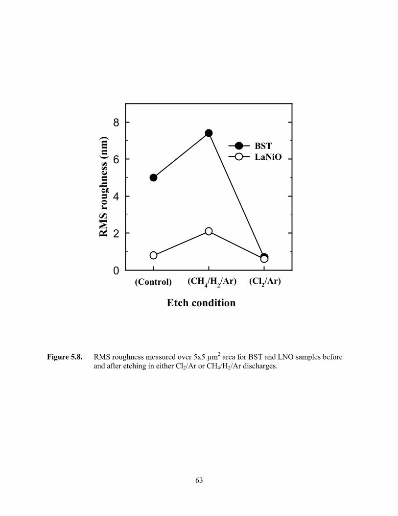
63
Figure 5.8. RMS roughness measured over 5x5 µm2 area for BST and LNO samples before and after etching in either Cl2/Ar or CH4/H2/Ar discharges.
Etch condition
RM
S ro
ughn
ess (
nm)
0
2
4
6
8
BSTLaNiO
(Control) (CH4/H2/Ar) (Cl2/Ar)

64
6. Studies of the Doped Hexaborides
(F. Sharifi)
Over the last year, our efforts have focused on a new class of ferromagnetic materials that
have been discovered in studies of doped hexaborides of the alkaline earths. A surprisingly
robust weak ferromagnetism has been found both in electron and hole doped CaB6 at a carrier
concentration of approximately 0.005 e/unit cell. These materials raise not only interesting
fundamental questions regarding the nature of magnetic ordering, but suggest as well unusual
device possibilities.
The alkaline earth and light rare earth hexaborides are highly refractory materials that
crystallize in a simple cubic CsCl-type array of regular B6 octahedra and metal atoms. These
materials possess a low carrier density, high carrier mobility, and long mean free path. Band
structure calculations suggest that the hexaborides of the divalent metals are semi metallic, with
very small direct overlap of a conduction and a valence band of different symmetry at the X-
points in the Brillouin zone. In the presence of ferromagnetism, this band structure may result in
a large degree of spin-polarized carriers at the Fermi level. The internal Zeeman splitting of the
upper band can enhance the direct overlap of the majority band and cause the minority band to
be semiconducting [Figure 6.1]. Magnetization studies with bulk single crystals have shown that
in CaB6, both the hole-doped compound Ca1-δB6 and the electron doped compound
Ca0.995La0.005B6 are ferromagnetic. In electron-doped Ca0.995La0.005B6, the ferromagnetism has a
maximum moment of 0.07µB/La with a Curie temperature of 600 K. This is of course entirely
unexpected and falls outside the usual models for magnetic ordering in metals. Since these
materials couple low carrier densities with ferromagnetism, they may be excellent candidates for
field gating experiments, where the ferromagnetism is controlled directly through modulation of
carrier density [Figure 6.2]. We have performed a series of transport, magneto-transport, and

65
Hall measurements to characterize this novel material. The results of these measurements are
described below.
(a) Transport Results
The transport characteristics of these materials are extremely sensitive to the degree of
band overlap (if any) and the position of the Fermi level. Our measurements indicate that the
undoped material is essentially a small band gap semiconductor with a temperature dependent
resistivity shown in Figure 6.3c. In the La-doped material, the addition of electron carriers raises
the Fermi level to the upper band, leading to metallic behavior with a weak temperature
dependence, as shown in Figure 6.3a. Similarly, hole-doping this material through removal of
Ca decreases the Fermi level, placing it in the lower band, again leading to a weak metallic
behavior as shown in Figure 6.3b.
For the metallic compounds, the rather weak temperature dependence implies that
electron-phonon scattering may be quite constrained. This is not surprising in view of the
peculiar band structure of this material, where the metallicity arises from quite narrow bands.
Any scattering mechanism would have a constrained phase space since the final momentum
values of the scattered electrons have to lie within this narrow pocket for the process to be
allowed.
(b) Magneto-transport Results
Magneto-transport studies are a useful tool for elucidating the mechanisms behind
ferromagnetism in many materials. For example, the magnetoresistance of an itinerant
ferromagnet, the category into which we would suspect doped CaB6 to fall, is negative and linear
with magnetic field. As illustrated in Figures 6.4 - 6.6, data taken on these compounds show a
negative magnetoresistance that exhibits curvature at low fields but becomes linear at higher

66
fields. These findings imply additional interactions that distinguish these materials from
ordinary itinerant systems.
(c) Hall Measurements
The Hall effect is useful in the determination of the carrier sign and concentration. In a
Hall measurement, current is injected longitudinally while a magnetic field is applied normal to
the plane of the sample. Charge builds up on one side of the sample as the Lorentz force acts on
the charge carriers. As a result, a potential can be measured in-plane and perpendicularly to the
current path, as illustrated in Figure 6.7.
The sign of this Hall voltage indicates the sign of the carriers and can be used to calculate
the carrier concentration as follows:
neRwhere
diHRV H
HH
1, ==
A compensated band structure complicates the expression for the Hall coefficient, RH.
When both electrons and holes contribute to the electrical transport of a material, the Hall
coefficient must include the electron and hole densities, as well as the corresponding mobilities:
( )2
22
np
npH npe
npR
µµµµ
+
−=
Hall effect measurements are useful to the determination of the band structure of CaB6.
As shown in Figure 6.8, data already taken indicate a compensated band structure in which both
holes and electrons play a role in transport. The magnitude of the carrier density is clearly
determined by the position of the Fermi level, where a reduction in the carrier density occurs as
the Fermi level is shifted downwards in the band in this material.

67
The anomalous Hall effect is commonly seen in many ferromagnetic systems. In addition
to the conventional Hall resistivity, a term proportional to the magnetization appears:
MRBRR SoH π4+=
This term arises due to the internal field present within the ferromagnet. In ferromagnets that
exhibit hysteresis in magnetization with field, manifestation of this term in Hall data is marked
by a break in the slope accompanied by a non-zero intercept.
Since the magnetization data taken on doped CaB6 features hysteresis with field, a
hysteretic anomalous Hall voltage is expected. In our data, hysteresis is seen in hole-doped
CaB6, as shown in Figure 6.9. This effect is only observed when the sample is zero-field cooled
and only during the first sweep in field. The saturation field is in good agreement with that
indicated in the magnetization curve shown in Figure 6.10. To observe the anomalous signal in
such a weakly ferromagnetic system requires extremely careful measurement techniques over
small magnetic field ranges.
(d) Summary
Our measurements indicate an unusual mechanism for magnetism exists in these
materials. Due to the low carrier densities, the hexaborides present a clear opportunity for a new
class of materials where the ferromagnetism can be directly controlled through external field
gating. As such, these materials can be classified as novel magnetic semiconductors, allowing
for their use in the newly emerging field of spin-based electronics.

68
Figure 6.1 Figure 6.2
Figure 6.3 (a-c)
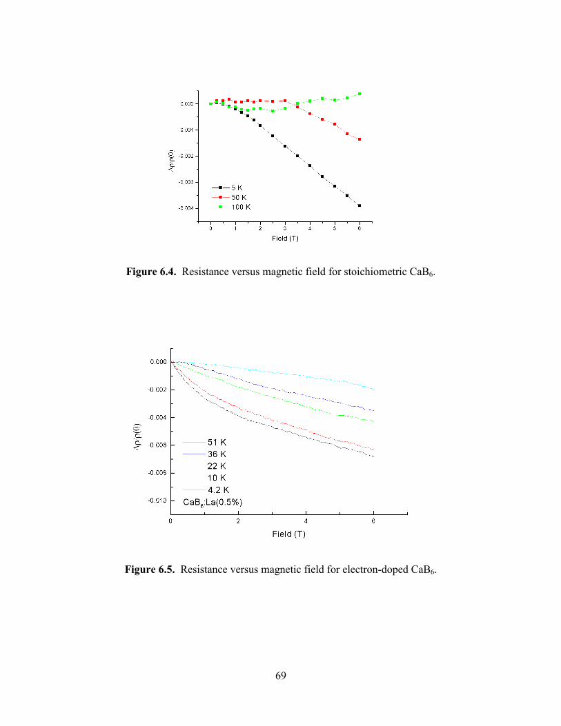
69
Figure 6.4. Resistance versus magnetic field for stoichiometric CaB6.
Figure 6.5. Resistance versus magnetic field for electron-doped CaB6.
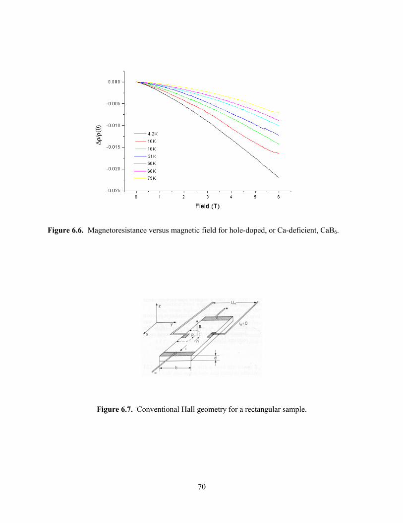
70
Figure 6.6. Magnetoresistance versus magnetic field for hole-doped, or Ca-deficient, CaB6.
Figure 6.7. Conventional Hall geometry for a rectangular sample.

71
Figure 6.8. Effective carrier concentration versus temperature for electron-doped, hole-doped, and undoped CaB6. Note that the carrier concentration shown here is defined as RH/e and may be complicated by compensation, i.e. may not represent only electron-like transport.
Figure 6.9. Hysteresis in Hall voltage versus magnetic field for Ca1-B6, which shows the
saturation field to be roughly 2500 Oe.
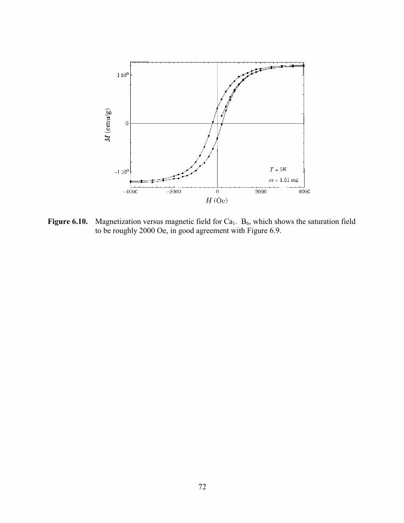
72
Figure 6.10. Magnetization versus magnetic field for Ca1-B6, which shows the saturation field
to be roughly 2000 Oe, in good agreement with Figure 6.9.
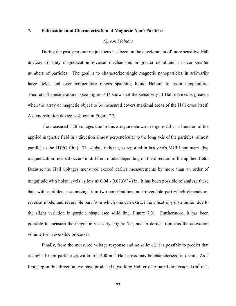
73
7. Fabrication and Characterization of Magnetic Nano-Particles
(S. von Molnár)
During the past year, our major focus has been on the development of more sensitive Hall
devices to study magnetization reversal mechanisms in greater detail and in ever smaller
numbers of particles. The goal is to characterize single magnetic nanoparticles in arbitrarily
large fields and over temperature ranges spanning liquid Helium to room temperature.
Theoretical considerations (see Figure 7.1) show that the sensitivity of Hall devices is greatest
when the array or magnetic object to be measured covers maximal areas of the Hall cross itself.
A demonstration device is shown in Figure 7.2.
The measured Hall voltages due to this array are shown in Figure 7.3 as a function of the
applied magnetic field in a direction almost perpendicular to the long axis of the particles (almost
parallel to the 2DEG film). These data indicate, as reported in last year's MURI summary, that
magnetization reversal occurs in different modes depending on the direction of the applied field.
Because the Hall voltages measured exceed earlier measurements by more than an order of
magnitude with noise levels as low as 0.04 - 0.07µV/ Hz , it has been possible to analyze these
data with confidence as arising from two contributions, an irreversible part which depends on
reversal mode, and reversible part from which one can extract the anisotropy distribution due to
the slight variation in particle shape (see solid line, Figure 7.3). Furthermore, it has been
possible to measure the magnetic viscosity, Figure 7.4, and to derive from this the activation
volume for irreversible processes.
Finally, from the measured voltage response and noise level, it is possible to predict that
a single 10 nm particle grown onto a 400 nm2 Hall cross may be characterized in detail. As a
first step in this direction, we have produced a working Hall cross of areal dimension 1•m2 (see

74
Figure 7.5) onto which a portion of a 4x4 particle array has been grown. This device is perfectly
capable of measuring the ~7 particles which contribute to the signal and detailed measurements
are underway. We have also, over the past year, installed and made operational a new electron
beam lithographic tool with line resolution of order 20 - 30 nm. Attempts to fabricate Hall
devices of these dimensions are underway in GaAs/GaAlAs heterostructures and will be
extended to InAs quantum well structures operable at room temperature.

75
Figure 7. 1. Comparison of Hall voltages. Calculations were performed by assuming Hall
crosses of different sizes (circles, lower axis). Array and Hall cross were either assumed to be aligned with their centers (closed circles) or with one of their corners (open circle). All triangles represent experimental results (see text). In addition, the calculated Hall voltage for different separations between particles and 2DES is shown (crosses, upper axis).
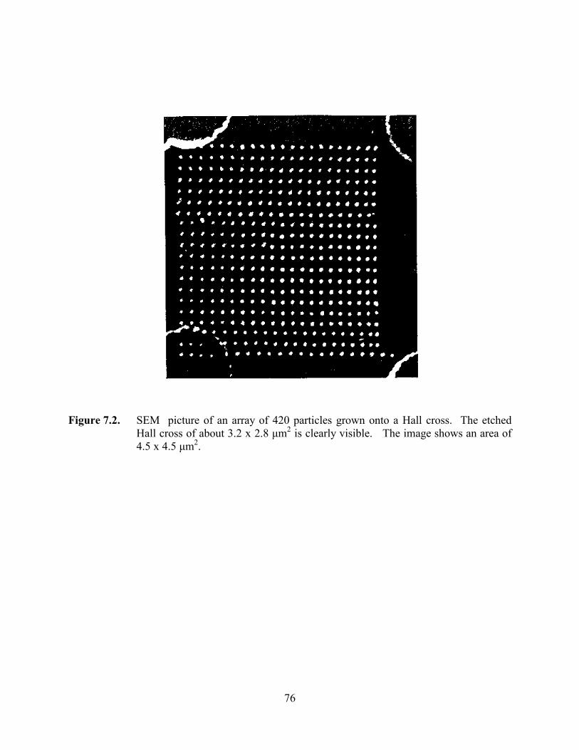
76
Figure 7.2. SEM picture of an array of 420 particles grown onto a Hall cross. The etched Hall cross of about 3.2 x 2.8 µm2 is clearly visible. The image shows an area of 4.5 x 4.5 µm2.
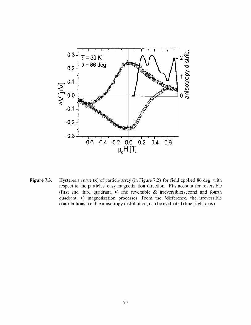
77
Figure 7.3. Hysteresis curve (x) of particle array (in Figure 7.2) for field applied 86 deg. with respect to the particles' easy magnetization direction. Fits account for reversible (first and third quadrant, •) and reversible & irreversible(second and fourth quadrant, •) magnetization processes. From the "difference, the irreversible contributions, i.e. the anisotropy distribution, can be evaluated (line, right axis).

78
Figure 7. 4. Measured time dependence of the total polarization under different conditions.
The line presents the result of a fit to a logarithmic law.

79
Figure 7.5. SEM images of a small array grown onto a Hall cross of 1 x 1 •m2 (images size
1.1 x 1.5 •m2, one current leg can be recognized on the top.
80
8. Interface Phenomena and Screening Length Determination in Tunnel Junction Capacitors
(A. F. Hebard, K. T. McCarthy, D. Temple)
As electronic devices shrink to nanoscale size and their components become increasingly
close spaced, it becomes imperative to understand the new physics that becomes manifest at
reduced length scales. For example, when two parallel metal plates are placed in close proximity
(see inset of Figure 8.1) with a dielectric of thickness d separating them, the capacitance deviates
sharply from the value that would be expected from purely geometrical considerations. This
deviation occurs because, in addition to the voltage drop across the insulator separating the
plates, there are also voltage drops across the two metal-insulator interfaces. The extra
capacitance associated with these voltage drops is called the interface capacitance, Ci, and it
manifests itself as an additional capacitance in series with the geometrical capacitance, Cg.
The interface capacitance can be experimentally determined by plotting the reciprocal of
the measured capacitance, Cm, versus the dielectric spacing, d, and then extrapolating the linear
dependence to d=0 to find the intercept, Ci-1. Since capacitors adding in series obey the relation,
C C Cm i g− − −= +1 1 1 , the linear dependence arises because Cg is inversely proportional to d and Ci
depends only on interface properties. An example of this linear dependence is shown in the
Figure 8.2 plot of the thickness dependence of the reciprocal capacitance of seven different
Si/SiO2/Ni trilayer sandwiches with thermally grown (950°C) oxide thicknesses ranging from 35
to 400Å. The substrate is a (100) oriented n-type device grade silicon wafer with resistivity on
the order of 0.1Ωcm.
An extrapolation of the linear fit in Figure 8.2 to the negative intercept on the abscissa
gives a direct measure of the “thickness” d0 of the interface capacitance. This thickness includes
contributions from both interfaces. Accordingly, if the actual dielectric thickness d is less than

81
d0, then the interface capacitance dominates over the geometrical capacitance and properties such
as the ac loss (dispersion) are dominated by interface processes rather than bulk processes
associated with the dielectric. Such a situation is shown in Fig. 1, which reveals considerable
dispersion in the capacitance of an Al-AlOx-Al tunnel junction capacitor having a thermally
oxidized barrier with thickness on the order of 20 Å. This is considerably thinner than the d0=50
Å inferred from a set of measurements on similar structures with different dielectric spacings.
We note that the dispersion is pronounced down to frequencies as low as 0.001 Hz and that there
is no evidence of a loss peak at these low frequencies. We surmise that the filling and emptying
of interface trap states is responsible for this dispersion. This conclusion is supported by our
observation that for thicker dielectrics the dispersion is considerably less, as would be expected
since the capacitance in this regime is dominated by the frequency-independent properties of
bulk aluminum oxide.
Frequency dependence at such low frequencies can have considerable implications for
the temporal stability of devices that incorporate tunnel junctions and related structures.
Accordingly, it is important to understand in detail the interface phenomena that contribute to the
magnitude of d0 and the accompanying losses associated with time-dependent excitations. The
Thomas-Fermi screening length, which depends on the density of states in the metal electrodes,
is an important starting point. Film roughness, impurities, and the number and type of interface
trapping sites are also important and are presently being investigated.
If magnetic electrodes are involved, then there is an additional contribution to the
interface capacitance that is predicted to arise from the exchange interactions between the spin-
polarized carriers of the magnetized electrodes. Our preliminary attempt to confirm this
prediction is shown in Figure 8.3, which is a plot of the d0’s obtained from a series of Si/SiOx/M

82
(M=Fe, Ni, Co) trilayer structures, all made on the same n-type silicon wafer. Each point on this
plot represents a series of measurements similar to that shown in Fig. 2 on seven different
samples. The values for d0 are obtained by extrapolation in the same way as discussed above.
The thickness of the depletion layer in the doped silicon depends on voltage bias. Accordingly,
d0 is minimum for each series with different counter electrode M at positive voltage where the
depletion capacitance is maximum (strong accumulation). Assuming that the differences in d0
arise only from the differences in the counter electrodes (assuming everything else remains
equal), we tentatively conclude that the screening lengths of Fe, Ni and Co are significantly
different. Further work must be done to show that these differences arise from the predicted spin-
dependent surface screening in the ferromagnetic electrodes. We anticipate that these studies
may have important implications for tunneling magnetoresistive (TMR) devices and related
structures with magnetic electrodes. The effects will be enhanced with low-carrier density
magnetic materials having relatively large screening lengths.

83
10-2 100 102 104 1061.00
1.50
2.00
2.50
3.00AL-AL2O3-AL
C1 (µ
F/cm
2 )
Frequency (Hz)
V /σ
0 d
d + d o
Figure 8.1. Frequency dependent capacitance of an Al-Al2O3-Al tunnel-junction trilayer structure. The inset shows schematically the voltage drops across the two interfaces and the dielectric (shaded).
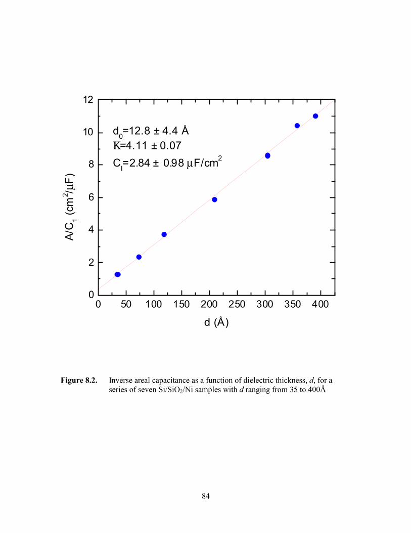
84
Figure 8.2. Inverse areal capacitance as a function of dielectric thickness, d, for a series of seven Si/SiO2/Ni samples with d ranging from 35 to 400Å
0 50 100 150 200 250 300 350 4000
2
4
6
8
10
12
d0=12.8 ± 4.4 ÅΚ=4.11 ± 0.07CI=2.84 ± 0.98 µF/cm2
A/C
1 (cm
2 /µF)
d (Å)
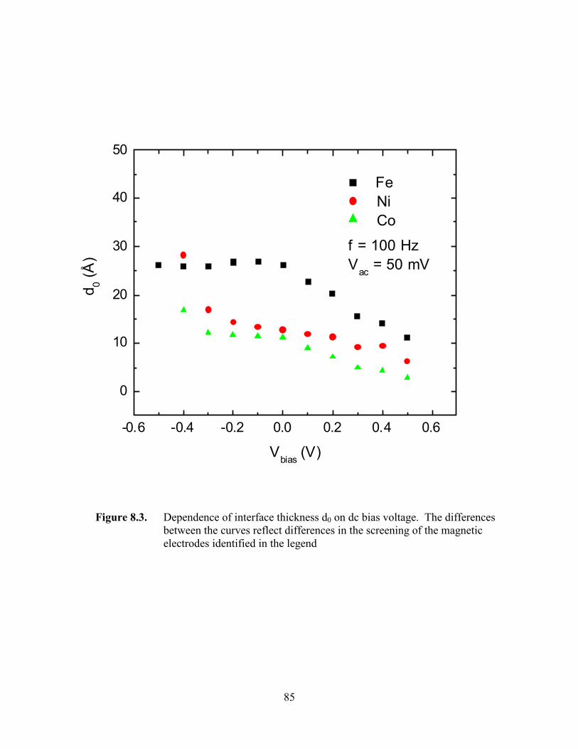
85
-0.6 -0.4 -0.2 0.0 0.2 0.4 0.6
0
10
20
30
40
50
Fe Ni Co
f = 100 HzVac = 50 mV
d 0 (Å)
Vbias (V)
Figure 8.3. Dependence of interface thickness d0 on dc bias voltage. The differences between the curves reflect differences in the screening of the magnetic electrodes identified in the legend
86
9. Hysteresis and Relaxation Behavior in GMR Multilayers
(A. F. Hebard, N. Theodoropoulou, A. K. Majumdar, D. Temple)
The work reported in this section is a continuation of collaborative work between UF and
MCNC on the characterization of GMR multilayer stacks prepared by ion beam sputter
deposition. The effort at MCNC has focused on deposition and structural characterization and the
effort at UF has been on providing rapid feedback to MCNC on the electrical
(magnetoresistance) and magnetic (magnetization) properties of the fabricated multilayer
structures. This collaboration has produced GMR structures with properties comparable to the
best structures fabricated using sputter deposition techniques. The magnetoresistance of a typical
Fe/Cr multilayer [Fe(20Å)/Cr(10 Å)]×30 made by ion beam sputter deposition (Xenon, 900V,
20mA) is shown in Figure 9.1. The chromium spacer thickness is chosen to insure that the
ferromagnetic domains in adjacent iron films are antiferromagnetically coupled. Thus in low
field, when the spins of adjacent layers are antiparallel, spin-flip scattering gives rise to a higher
resistance than occurs at high fields when the spins are parallel.
In our magnetization studies of these structures, we have observed a heretofore-
unreported hysteretic behavior in the low field (H<1000 Oe) region. The evidence for hysteresis
is shown in the temperature-dependent magnetization data of Figure 9.2. We note from these
data that the magnetization at a given temperature and field is history dependent, i.e., the value
depends on whether it has been zero-field-cooled (ZFC) or field-cooled (FC). For a given field
there is an irreversibility temperature Tc(H), below which there is hysteresis (irreversible
behavior) and a difference between the FC and ZFC curves, and above which, there is no
hysteresis, and the FC and ZFC curves overlap. The irreversibility temperature is field

87
dependent and thus defines a critical field, which separates irreversible from reversible behavior
and which has the temperature dependence shown in Figure 9.3.
Relaxation dynamics in the hysteretic region are extremely slow. This is shown in Figure
9.4 where the sample has been field cooled to 55K in a field of 200 Oe. After turning off the
field, the relaxation towards the ZFC state is observed to have logarithmic time dependence as
shown in the figure. Assuming the persistence of this logarithmic rate, the time taken to
complete the transition is calculated to be greater than the age of the universe.
The temperature dependence of the logarithmic rates at selected fields is shown in Fig. 8.
As temperature increases the logarithmic creep rate decreases and approaches zero near Tc(H).
This “critical slowing down” with increasing temperature is common to spin-glass and related
systems where disorder and frustration are prominent. This behavior is distinctly different from
the “magnetic viscosity” effects observed when a field is applied to a bulk material such as
Alnico and the logarithmic creep rate is observed to increase with temperature. With logarithmic
rates it is straightforward to show that the time, tF, the system takes to get from the ZFC to the
FC state (or vice verse) is exponentially sensitive to the difference (FC-ZFC) between the two
states divided by the logarithmic creep rate. Since with increasing temperature the separation
between states decreases faster than the logarithmic rate, the time tF, which at low temperatures
can be longer than the age of the universe, decreases toward zero at the irreversibility
temperature. In the language of Zeno, the tortoise always wins the race with the hare.
The observed behavior is different from conventional spin glasses where the
irreversibility temperature usually delineates the boundary between a low-temperature frustrated
system of exchange-coupled spins and a high-temperature paramagnetic system of independent
spins. In the GMR samples the boundary is between antiferromagnetically coupled

88
ferromagnetic domains that are predominantly antiparallel at low fields (T<Tc) and parallel, but
still antiferromagnetically coupled, at higher fields (T>Tc). Alternatively, these dynamical effects
are related to thermally blocked relaxation of superparamagnetic grains in our multilayers.
Understanding these dynamics is essential for the achievement of long time stability in devices
based on GMR effects.
-20 -10 0 10 20
-0.20
-0.15
-0.10
-0.05
0.00
10 K
300 K
Mag
neto
resi
stan
ce (%
)
H (kOe)
Figure 9.1. Percent change in resistance of an iron-chromium 30-layer GMR stack [Fe(20Å)/Cr(10Å)] at the indicated temperatures as a function of magnetic field applied in a direction parallel to the plane of the film.
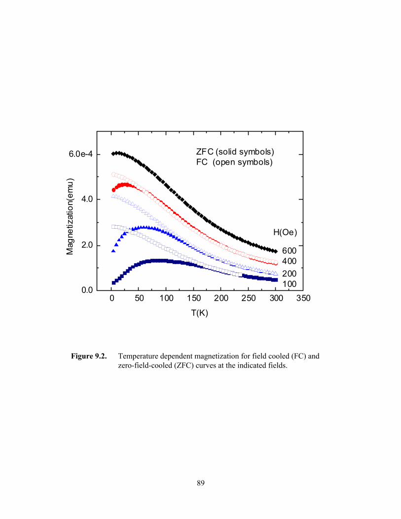
89
0 50 100 150 200 250 300 3500.0
2.0
4.0
6.0e-4 ZFC (solid symbols)FC (open symbols)
H(Oe)
600
100200400
Mag
netiz
atio
n(em
u)
T(K)
Figure 9.2. Temperature dependent magnetization for field cooled (FC) and zero-field-cooled (ZFC) curves at the indicated fields.

90
0 50 100 150 200 250 3000
100
200
300
400
500
Mag
netic
Fie
ld (O
e)
Temperature (K)
Figure 9.3. Temperature dependence of the irreversibility field.

91
10 100 1000 100004.48
4.50
4.52
4.54
4.56
4.58e-4FC in 100 Oe to 55KTurn off field at t=0
M (e
mu)
Time (sec)
Figure 9.4. Time dependence of the magnetization after cooling the sample to 55K in a field of 100Oe and then setting the field to zero.

92
0 50 100 150 2000.0
1.0
2.0
3.0
4.0
5.0
6.0
7.0e-2
Loga
rithm
ic R
ate
Temperature(K)
B50 B100 B150 B200 B300
Figure 9.5. Logarithmic rate (magnetic viscosity) as a function of temperature at the indicated magnetic fields.

93
10. Superparamagnetic-ferromagnetic Transition
(R.C. Dynes)
We have studied the superparamagnetic-ferromagnetic transition of small Ni particles as
a function of T and particle size. The transition has been detected in magnetoresistance and
magnetization of thin discontinuous films of Ni quench-condensed on an isolating substrate.
With increasing coupling between grains (
≈100 Ao
in size) we observe a crossover from non
hysteretic to hysteretic behavior in magnetoresistance and magnetization. This crossover
correlates with a transition from isolated grains to larger clusters. With increasing cluster size,
the blocking temperature increases and the material becomes a ferromagnetic. This 2
dimensional crossover allows a study of the interactions between magnetic-nanoparticles.
(a) Micro SQUIDS
We have developed the technology to manufacture micro SQUIDS to be used to study
magnetic nanoparticles. We have fabricated SQUID loops approximately equal to 2 microns on
a side using e-beam lithography techniques. The sensitivity of these SQUIDS is such that they
are capable of detailing a single ferromagnetic nanoparticle (a few hundred angstroms in
dimension) and will be used to study the switching characteristics of ferromagnetic particles.
Attached is a figure describing the geometry of these SQUIDs and a typical Ic(B) pattern at 1.5K
for an Al SQUID.
(b) Superconducting and Spin-dependent Tunneling Using native Oxide Barriers
on CoFe Thin Films
Spin dependent tunneling has been demonstrated in native oxide barriers of CoFe. Using
a superconductor as a counter electrode, it has been clearly demonstrated that the dominant
conduction mechanism for CoFe to the superconductor is electron tunneling through the native
94
oxide. Replacing the superconductor with the ferromagnetic Co results in a magnetoresistance of
≈ 4%. This is the largest value to date in a spin-dependent tunnel junction using a native oxide
barrier on a ferromagnet. Junction quality depends strongly on the deposition condition for the
top electrode.
11. Length Scale of Magnetism
(F. Hellman)
The goal of this work is to understand the length scale and magnitude of the magnetism
induced in a non-magnetic or nearly magnetic material by proximity to a magnetic material,
particularly in metallic materials. This is an effect that is well understood in superconducting
materials and has led there to practical devices. In magnetism, the effect is less well understood
and is generally believed to be extremely local. However, it is clear that in materials, which are
nearly magnetic, such as Pd or Pt, this length scale will be much longer. As little as 1% Co in Pt
leads to a ferromagnetic Curie temperature of over 5K, indicative of the ability of Co to induce
magnetism in Pt on a relatively long length. We have used UHV techniques to prepare vapor-
deposited Co-Pt and related Ni-Pt and Co-Pd alloys of various compositions and Curie
temperatures. These alloys spontaneously form a nanostructured incoherent multilayer, causing
perpendicular anisotropy to occur in a nominally fcc material. This compositional
nanostructuring has to date not been directly measured, although asymmetric short-range
chemical order has been seen in EXAFS. By controlling the growth parameters, we can control
the development of this nanostructure and measure its effect on the magnetic properties. In the
most extreme case, the magnetization versus temperature exhibits a broad (several hundred
degrees in width) and nearly linear temperature dependence. We are working at present on
preparing multilayers in order to determine the nature of the nanostructure which could give rise

95
to the observed broad M(T) in the spontaneously nanostructured material. We are also at present
completing work on thermodynamic characterization of several nanostructured magnetic
materials.
12. Fabrication and Characterization of Magnetotransport in Colossal Magnetoresistive Oxide Films and Hybrid Structures
(Srinivas V. Pietambaram, Jaeyoung Choi, D. Kumar, Hyoung-June Kim, Rajiv K. Singh and S. J. Pearton)
The continually increasing demand for magnetic information storage and retrieval has
driven a significant worldwide effort to improve the performance of relevant hardware
components. As the areal density continues to increase, more sensitive materials and innovative
structures will be required to detect the decreasing magnetic fringe-fields emanating from the
media. Doped LaMnO3 is being examined as a possible next generation magnetoresistance
sensor material. Over an appreciable range of doping, these materials exhibit a very large
magnetoresistance effect at temperatures close to where they undergo a ferromagnetic-
paramagnetic transition. The basic manganite, LaMnO3, is antiferromagnetic and insulating.
Partial doping of La sites with alkaline earth cations in LaMnO3 results in a Mn3+/Mn4+ mixed
valence state which is responsible for both metallic conductivity and ferromagnetism in
accordance with double exchange interaction. Although, structural and magnetotransport
properties of manganite thin films have been found to vary significantly with change in process
parameters, detailed and systematic study is missing in the literature. Besides, the effects of
crystallinity and oxygen content of the films on the properties is not clearly resolved. The highly
spin polarized nature of these materials can be used for developing new structures having a high
MR ratios.

96
(a) Oxygen Content and Crystallinity Effects in Pulsed Laser Deposited Lanthanum Manganite Thin Films
The effects of oxygen in manganite film have been a focus since the discovery of
extraordinary magnetotransport in this kind of materials. There is no quantitative relation
between the oxygen content and the magnetic and transport properties in thin films till date due
to the difficulty in the determination and control of oxygen content. Substrate temperature,
oxygen partial pressure, and deposition rate could have an effect on the oxygen content of the
film severely. Vacuum annealing can produce a deficiency in oxygen while excess oxygen can
be produced by annealing in oxygen. All these indicate that oxygen content can be flexible in
manganese oxides. In the early studies of CMR materials, a post deposition anneal in oxygen at
high temperatures was critical for achieving large magnetoresistance. However, it was not known
whether the improvement was due to grain refinement through grain growth and enhancement in
the crystallinity of the films or due to oxygen incorporation. Improvement in the crystallinity and
grain growth enhances the properties of the oxide thin films. Systematic post deposition heat
treatments were performed to deconvolute the effects of oxygen content and grain growth in
Lanthanum Manganite thin films.
Bulk La0.7Ca0.3MnO3 (LCMO) was prepared by a ceramic method. The required
quantities of respective oxide or carbonate powders were mixed and sintered at 1400°C for 24
hours. Six LCMO films with a thickness of 1500 Å were grown in situ on (100) LaAlO3
substrates using a pulsed laser ablation system. To eliminate other external effects, all the
substrates were placed side by side on sample holder. All the films were characterized to see if
the properties were identical before performing any post deposition heat treatments. A 248 nm
KrF pulsed laser with 5 Hz repetition rate and 1.6 J/cm2 energy density was used. A substrate
temperature of 700°C and oxygen pressure of 250 mTorr were used during the deposition of the
97
films. Following the deposition, the films were cooled down to room temperature at a rate of
10°C/min in 400 Torr of oxygen. After the initial characterization to check the identical
properties, the films were subjected to the following post deposition anneals – (i) annealing in
oxygen at 900°C for 4 hrs, (ii) annealing in argon at 900°C for 4 hrs, (iii) annealing in oxygen at
500°C for 12 hrs, (iv) annealing in argon for 12 hrs and (v) annealing in vacuum at 850°C for
half-an-hour.
XRD patterns of the films subjected to various anneals are shown in Figure 12.1. From
the Figure it is clear that all the films have single phase with (00l) peaks with l = 1 and 2. The
presence of only sharp (00l) peaks indicates the highly textured growth of all the films on (100)
LaAlO3 substrate. The lattice parameters for the films with no anneal, 900°C oxygen anneal and
900°C argon anneal were found to be 3.8632, 3.8337, and 3.8444 Å respectively. XRD patterns
of 500°C oxygen and argon annealed films were similar to that of as-deposited films. The films
annealed in oxygen and argon show a decrease in the full width at half maximum (0.1°)
compared to the as-deposited film (0.25°) indicating these films are more crystalline.
The variation of electrical resistance in zero and applied field (5T) as a function of
temperature for the films subjected to various anneals are shown in Figure 12.2. All the films
were grown under identical conditions so that film thickness, oxygen contents of all the films and
other external effects (before anneals) could be kept identical. It is important to keep these
parameters identical in order to reveal the effects of the magnetotransport properties in these
films. According to the variation of resistance shown in Figure 12.2., all the films (except
vacuum annealed one) have similar qualitative magnetotransport behavior. That is, all the films
undergo an insulator-to-metal (I-M) transition as the temperature is lowered down and the
resistance of all the films is suppressed significantly with the application of magnetic field. The
98
suppression in film resistance in each case is maximum near the resistivity peak in zero field as
observed frequently by others in several manganite systems. The MR ratios of the films were
calculated using the data in Figure 12.2. The MR ratios obtained are plotted in Figure 12.3 as a
function of temperature at 5T.
The as-deposited films show an I-M transition at 260 K and a MR ratio of 190% in 5T.
The films subjected to 500°C oxygen anneal and 500°C argon anneal show little change in I-M
transition and MR ratio. This shows that 500°C is not a sufficiently high enough temperature to
affect the oxygen content, grain growth and crystallinity. The films subjected to 900°C oxygen
anneal show an improvement in transition temperature (290 K) but a marginal enhancement in
the MR ratio (225%). The films subjected to 900°C argon anneal show slight increase in the
transition temperature (270 K) and significant enhancement in the MR ratio (525%). The films
subjected to vacuum anneal have shown deteriorated properties (insulating down to 10 K).
Annealing of the films at high temperature lead to two simultaneous effects – removal of
oxygen from the film and grain growth and improvement in crystallinity. Films subjected to
500°C oxygen and argon anneals show little effect on the transition temperature or MR ratio.
This temperature is not high enough for either oxygen incorporation or to cause grain growth.
Further, no observable differences were found from the XRD patterns of these films as compared
to the as-deposited films. Hence these anneals have no effect on the properties of the film.
Films annealed in oxygen at 900°C show an increase in the transition temperature from
260K to 290K. The resistance of the films also decreased compared to as deposited films. These
effects can be understood from the increase in the oxygen content of the films. The
ferromagnetic transition is strongly determined by the number of Mn4+ ions. The mixed
Mn3+/Mn4+ valence is believed to give rise to both ferromagnetism and metallic behavior in
99
LCMO films, and to be responsible for the occurrence of colossal magnetoresistance. As oxygen
is incorporated in the film two distinct reactions occur: contraction of the lattice, as evidenced by
x-ray diffraction; and gain in the O2- ions. Gain of oxygen ions should lead to changes in
magnetotransport similar to those resulting from the application of external pressure. Under
applied pressure the lattice contracts while transition temperature (Tc) increases and resistance
decreases. These results can be explained by an enhancement in the Mn-Mn electron transfer
probability as the average lattice spacing is decreased. An increase in the transfer probability
should lead to an enhanced ferromagnetic correlations and increased carrier mobility between
adjacent Mn ions. This leads to a higher Tc and lower resistance. The second effect relating to
oxygen arises from the requirement of charge neutrality within each unit cell. The chemical
formula for LCMO can be written as La1-x3+Cax
2+Mn1-x+2δ3+ Mnx-2δ
4+O3-δ2-. Therefore, each
oxygen incorporated into LCMO should lead to a conversion of Mn3+ ions to two Mn4+ ions. The
carriers in LCMO are holes whose concentration is proportional to the Mn4+ concentration.
Therefore, the incorporation of oxygen should increase Mn4+ concentration, which leads to an
increase in the carrier concentration, and hence decrease in the resistance.
However, annealing at high temperatures also causes grain growth which affects the
domain size. These effects can be isolated by annealing the films at elevated temperature in an
ambient other than oxygen such as argon. Films subjected to argon annealing at 900°C show
marginal increase in the transition temperature. The resistance of the films is higher than that of
the oxygen annealed films. The increase in the resistance of the films can be attributed to the loss
of the oxygen from these films. The interesting feature of high temperature argon annealed films
is significantly high MR ratio observed in these films. This may be attributed to the increase in
the domain size. Near the domain-wall boundaries, the pairs of spins of Mn3+ and Mn4+ may not

100
be parallel. As a result the electron transfer between pairs of Mn3+ and Mn4+ ions across the
domain wall is difficult and the resistance is high. Increase in the domain size reduces the
amount of domain-wall boundaries in a specified area. As a result, smaller fields are necessary to
align these domains; hence the suppression of resistance is much higher for a given magnetic
field and as such higher MR ratios. The marginal improvement in the transition temperature may
also be related to an increased domain size due to the smaller amount of domain-wall boundaries
and reduced resistance for the ferromagnetic alignment. The lattice parameter of argon annealed
films is higher than that of oxygen annealed films which indicates that the films have less
oxygen. However, the decrease in the lattice parameter in argon annealed films compared to as-
deposited films is not clearly understood. It seems that an increase in the domain size causes a
decrease in the lattice parameter.
Vacuum annealed samples undergo the most severe heat treatment. The loss of oxygen
from the film leads to the conversion of two Mn4+ ions to Mn3+ ions. The presence of critical
oxygen content is essential for the occurrence of metal to insulator transition (MI) in the LCMO
films. Observations made by others indicate that MI transition will disappear in the compound
La1-xCaxMnO3 with a Mn4+/Mn3+ ratio less than 0.17. In the vacuum annealed samples, there
may be a depletion of oxygen to the extent in which Mn4+/Mn3+ ratio is less than 0.17. Hence
these films show insulating behavior down to 10 K.
Low temperature (500°C) oxygen and argon anneals show little effect on the transition
temperature or MR ratio. High temperature (900°C) oxygen anneal shows a significant
improvement in the transition temperature while high temperature (900°C) argon anneal shows a
substantial increase in the MR ratio. The transition temperature is related to the oxygen content
while the MR ratio is affected by the domain size.

101
(b) Fabrication of Multi-Layered Structures
One of the distinguished features of La0.7Ca0.3MnO3 (LCMO) is a ferromagnetic half-
metallic state, where only the single spin band crosses the Fermi level. Such a half metallic state
can lead to 100% spin polarization of conduction carriers, which is much higher than that of
typical ferromagnetic metals such as Co, Ni, or Fe and their alloys. Nearly 100% of spin
polarization of various manganites such as LCMO and La0.7Sr0.3MnO3 (LSMO) have been
reported from spin polarized photoemission studies. One way of taking advantage of this highly
spin polarized nature of these manganites is a spin-dependent tunneling magnetoresistance
(TMR) of a magnetic tunnel junction (MTJ), since the TMR ratio is defined and given by
TMR (%) = (RAP – RP)/ RAP X 100 = 200 X P1P2/(1+ P1P2)
Where RAP and RP are the resistances in the antiparallel and parallel magnetic
configuration respectively and P1and P2 are the spin polarizations of the two electrodes. Spin
polarization P is the difference between the density of states (DOS) of spin-up (parallel to the
magnetization) and spin-down (antiparallel to the magnetization) electrons at the Fermi level.
Recently, TMR ratios up to 400% have been reported in LSMO/STO/LSMO trilayer
structure at low temperature (10 K). Despite of these large TMR values, the obstacle in these
systems is that large TMR values are observed at temperatures below 100 K, rapidly vanishing at
higher temperatures. Since this temperature is far below the Curie temperature of these
manganites (Tc of LCMO and LSMO are approximately 270 K and 370 K, respectively), this
premature decrease of TMR brings an important issue for understanding as well as practical
applications of these systems. Even though the cause of the rapid TMR loss with temperature is
not understood at this moment, the existence of surface dead layer with depressed magnetic order
at elevated temperatures is suspected. Since the magnetic properties of these materials are highly

102
sensitive to local crystal properties and the extrinsic strain field induced by lattice mismatch
among the grown layers, combination of selected material species, their crystal integrity, and
thickness of insulators will be critical for improving the TMR values as well as their temperature
dependency.
With this background, we have started investigating the characteristic TMR effects in
various LCMO/LAO/FM (FM = NiFe, etc) systems mainly as a function of deposition conditions
and layer thickness. In the first study, we have chosen La0.7Ca0.3MnO3 as a primary
ferromagnetic (FM) material, since it shows good ferromagnetic properties and is well optimized
in our lab. We have decided to use LaAlO3 as the barrier material because it gives good lattice
match with the LCMO base. NiFe was used as the top FM electrode. The choice of NiFe as a top
electrode could claim the following advantages. NiFe is a typical FM metal, which shows
superior soft magnetic properties. Low Coercivity value of NiFe, usually less than 10 Oe, as well
as typically observed squareness of M-H hysteresis give the wide range of antiparallel alignment
with the other electrode LCMO, which shows a coercivity values of 200 - 400 Oe. Also NiFe
grows pretty well on any substrate.
Thin films of Lanthanum calcium manganite (La0.7Ca0.3MnO3) were deposited on LaAlO3
substrates in a pulsed laser ablation system at a substrate temperature of 850°C and oxygen
pressure of 250 mTorr. Following the deposition, thin films of LaAlO3 were grown on
La0.7Ca0.3MnO3 in the same system. After the deposition, the films were cooled down to room
temperature at a rate of 10°C/min in 400 Torr of oxygen. Then NiFe films were sputter deposited
using UHV sputtering chamber.
The first requirement to observe TMR in a junction is the magnetic decoupling of the
electrodes, which allows the existence of an antiparallel configuration in a certain magnetic field

103
range as well as the parallel configuration at high field. We have measured the field dependence
of magnetization at 10 K for the structures with varying thickness of the barrier layer (shown in
Figure 12.4 (a), (b), (c) and (d)). We found that at least 10 A of barrier layer is necessary for
decoupling the two electrodes
We have then fabricated some shadow mask magnetic tunnel junctions to study the TMR
behavior. The shadow mask junctions were as shown in Figure 12.5. TMR values observed with
a shadow mask as described above were poor. The actual reason for this is not clearly
understood. One of the probable reasons may be that the interface resistance or the junction
resistance is lower compared to that of the sheet resistance of the electrode. In such a case CPP
resistance is no longer representative of the interface and would contain complex, current-
distribution limited resistance that is associated with the details of junction geometry. This is
especially true in case of magnetic oxide materials such as manganites whose resistivity can vary
two orders of magnitude between 4.2 K and ambient temperature. Another reason may be due to
the local pinhole shorts, which occur, when the thickness of the barrier layer is small. We need to
further investigate to understand these effects clearly.

104
Further studies are underway in which we are planning to fabricate smaller junctions
(thus having higher junction resistances) and study the TMR characteristics.
Inte
nsity
(arb
itrar
y un
its)
2-θθθθ
(degrees)30 40 50
(a)
(b)
(c)
(100
) film
(100
) sub
stra
te
(200
) film
(200
) sub
stra
te
(100
) film
(100
) film
(100
) sub
stra
te(1
00) s
ubst
rate
(200
) film
(200
) film
(200
) sub
stra
te(2
00) s
ubst
rate
Figure 12.1. XRD patterns of LCMO films, (a) no anneal, (b) 900 C oxygen anneal,and (c) 900 C argon anneal

105
Res
ista
nce
(Ohm
)
0
250
500
0100200300400
0300600900
1200
0
300
600
900
Temperature (K)0 100 200 300
0300600900
1200
(a)
(b)
(c)
(d)
(e)
Figure 12.2. Variation of electrical resistance with temperature for (a) noanneal, (b) 900 C oxygen anneal, (c) 900 C argon anneal, (d) 500 C oxygen anneal and (e) 500 C argon anneal (filled circle(0 T), filled diamond (2 T) and filled triangle (5 T))

106
Temperature (K)0 50 100 150 200 250 300 350
MR
ratio
(%)
0
100
200
300
400
500
600no anneal9000C O2 anneal9000C Ar anneal 5000C O2 anneal 5000C Ar anneal
Figure 12.3. Variation of MR ratio with temperature for the films

107
Magnetic Field (Oe)-1000 -500 0 500 1000
Mag
netiz
atio
n (e
mu)
-0.0015
-0.0010
-0.0005
0.0000
0.0005
0.0010
0.0015
no spacer
Magnetic Field (Oe)-1000 -500 0 500 1000
Mag
netiz
atio
n (e
mu)
-0.0015
-0.0010
-0.0005
0.0000
0.0005
0.0010
0.0015
5 A spacer
Magnetic Field (Oe)-1500 -1000 -500 0 500 1000 1500
Mag
netiz
atio
n (e
mu)
-0.0015
-0.0010
-0.0005
0.0000
0.0005
0.0010
0.001510A LAO
Magnetic Field (Oe)-1500 -1000 -500 0 500 1000 1500
Mag
netiz
atio
n (e
mu)
-0.0015
-0.0010
-0.0005
0.0000
0.0005
0.0010
0.0015
20 A LAO
Figure 12.4 Field dependence of magnetization of 10 K for LCMO/LAO/NiFe heterostructure with (a) no barrier, (b) 5Å barrier, (c) 10Å barrier and (d)20Å barrier.

108
LAO LAO
LCMLA
NiF
LCMLA
NiF
LCMO/L
Figure 12.5 Shadow mask junctions used for making TMR measurements.
109
13. Chemically Selective Remote Chemisorption on Metals - ICl/Al(111):
(Andrew C. Kummel)
The principle method of converting magnetic films into device is etching by halogen.
The first step in this process is the reaction of the halogen with the metal surface. We have bee
investigating this process using molecular beams techniques. The chemisorption of diatomic
halogens on aluminum and other low work function substrates is described as remote
dissociation; this process is analogous to the carefully studied alkali + ICl reactions. As the
halogen molecule approaches the surface, a harpooning electron is ejected from the surface to the
halogen molecule causing it to dissociate instantaneously. This process is associated with exoion
emission (ejection of negatively charged halogen atoms) that has a probability of 10-6 - 10-12
and exoelectron emission that has a probability of 10-3 - 10-9. However, little is known about
the dominant process. We have hypothesized that abstractive chemisorption should be very
common since an ejected halogen atom needs only a little kinetic energy to escape the attractive
potential of the surface compared the energy required for a halogen ion to escape its image
charge.
We have studied the chemisorption of ICl on Al(111) using non-resonant multiphoton
ionization, Auger spectroscopy, and sticking measurements to determine the chemisorption
dynamics. Using the reflection technique, we have determined that the sticking probability is
60% at high incident translational energy and is independent of the surface temperature. Using
Auger spectroscopy, we have determined that the ratio of iodine to chlorine on the surface is 5:1
for 0.05 to 1.2 eV ICl dosing of 110 K Al(111) at low coverage (<0.02 ML). This strongly
suggests that the dominant chemisorption process is abstractive chemisorption in which the
surface harpoons an electron preferentially to ICl molecules oriented with the iodine atoms

110
directed toward the surface. Upon formation of ICl-, the ICl dissociates to I- and Cl; the I-
chemisorbs to the surface while the Cl atoms are ejected back into the gas phase. To confirm
this hypothesis, we have used non-resonant MPI to detect the reaction products for 1.2 eV ICl on
110 K Al(111). As shown in Figure 13.1, in the incident beam we detect ICl+, the impurity I2+,
and the photodissociation products of I+ and Cl+, but in the scattered beam we only detect Cl+.
Therefore, when abstractive chemisorption occurs, it always results in chemisorption of iodine
and ejection of chlorine back into the gas phase. Harpooning preferentially occurs to the iodine
end of the molecule where the lowest unoccupied molecular orbital, *, is concentrated. When
ICl- dissociates in free space, it usually forms I + Cl- because Cl has a higher electron affinity
than I. However, since the iodine-end of ICl is closer to the surface during harpooning, the
iodine's electron affinity is increased by its image charge; therefore, the ICl + Al(111) results in
the preferential adsorption of iodine
Figure 13.1. MPI Spectra of ICl/Al(111) MPI Time of Flight Spectrum of the 1.2 eV ICl beam
reflected from the 110 K Al(111) surface. The left peak is just from photoelectrons. The only ion peak (Cl+) originates from the Cl abstractive chemisorption product. There is no detectable I+ peak. This proves that ICl/Al(111) abstraction always occurs by formation of an Al-I site and ejection of Cl back into the gas phase.

111
14. Abstractive Chemisorption of O2/Al(111)
(Andrew C. Kummel)
After a metallic magnetic film is deposited and exposed to air, an oxide layer forms. We
are using STM to determine how this process occurs. Our first studies have been on aluminum
since it is reactive and absorbates can be imaged with atomic resolution at low coverage at 300K
on Al(111). The chemisorption of O2 on Al(111) has been a source of great controversy because
the original STM experiment by Ertl's group showed that adsorption of thermal O2 on 300 K
Al(111) forms isolated oxygen atoms more than 80 Å apart. This was originally interpreted as
being the result of long range dissociation, but several theorists felt this was impossible due to
the large corrugation in the O/Al(111) potential. We have repeated this experiment using high
translational energy O2 molecular beams. We observe that at high translational energy, instead
of observing just single sites, we observe a 1:1 mixture of single and double sites (see Figure
14.1). We can be assured of the identity of the atomic O sites because we observe the exact
same O sites in the islands of oxygen atoms whose structure is known from LEED. We feel the
single sites are due to abstractive chemisorption while the double sites are due to dissociative
chemisorption; this would be consistent with theoretical investigations predicting that at high
translational energy the momentum towards the surface is sufficiently large that both abstraction
and long range dissociation are suppressed.

112
Figure 14.1. 50 Å x 50 Å STM Image of 0.5 eV O2/Al(111). This image shows the
chemisorption of O2 at very low coverage. There are three types of oxygen adsorbates, but all the oxygen appears at bright spots under these tip/tunneling conditions. There are single (“S”), isolated sites from abstractive chemisorption. There are double sites (“P” pairs) from dissociation. Finally there are islands of oxygen atoms. It seems that the chemisorption probability is greater near existing islands so the islands dominate with increasing coverage. At low translational energy the double sites are absent.
15. Measuring Mechanical Properties of Nanowires using depth Sensing and Force
Modulation
(S.A. Syed Asif, K.J. Wahl and R.J. Colton)
With the development of new nanostructured materials and continuing
miniaturization of engineering and electronic components, thin films and surface coatings,
there is a need to understand the mechanical properties of materials at the nanoscale.
Conventional uniaxial testing, macro or micro indentation techniques cannot be used for such
small volumes, and optical measurements of indent sizes are not possible. A logical approach
is to replace the optical microscope of a microindenter by an electron microscope. However
imaging of indents using electron microscopy suffers from the disadvantage of being time

113
consuming and can give large errors if the imaging conditions are not correct. To overcome
these problems, two different techniques and instruments have been developed: (1) the
atomic force microscope (AFM) and (2) the depth-sensing nanoindentation technique. While
both instruments can be used to determine materials properties at the nanoscale, each
technique has distinct advantages and disadvantages. However, we find that coupling the
AFM with depth-sensing indentation and AC force modulation can provide the best of both
techniques. In this report we will present our recent progress in developing quantitative,
surface sensitive nanoindentation techniques for nanostructures and thin films as well as the
applications of the force modulation technique to study adhesion and elastic properties of
thin compliant materials.
In this report we present a typical application of combined depth sensing and imaging
to study the deformation mechanics of nanostructures. Figure 15.1 shows an array of 500 nm
wide and 50 nm thick nickel nanowires on a silicon substrate. This topographic image was
obtained under displacement feedback. To study the mechanical response of this structure,
the image was used to locate and center the indentations on the Ni nanowire.
Figure 15.2 shows the load-depth response for both the Si substrate and Ni wire on Si.
From the unloading curve the modulus (130 GPa) and hardness (11 GPa) of the Si substrate
were calculated via the Oliver and Pharr method. The calculated value of hardness and
modulus agree with reported literature values. The load-depth curve for the Ni nanowire on
Si substrate shows substantial plastic deformation. To study the depth dependence of the
mechanical properties of the nanowires multiple indentation experiments were carried out at
different locations.
114
Figure 15.3 shows the superimposed load-depth response for Ni nanowire at different
loads and different locations. From each unloading curve the modulus and hardness were
calculated as a function of contact depth.
Figure15.4 shows the variation of modulus as a function of contact depth for the Ni
nanowire. The measured modulus is almost constant around 120 GPa, which is close to the
modulus of the Si substrate. The influence of the substrate, even for contact depths ~ 20 nm,
can be clearly seen. Figure15.5 shows the variation of hardness as a function of contact
depth. Unlike modulus, the hardness variation has a clear trend. At shallow depths the
measured hardness is close to that of Ni (1.5-2 GPa); and as the depth increases, the hardness
increases. To understand the possible reason for the increased hardness, an image of the
deformed zone was obtained using the hybrid nanoindenter. Figure15.6 shows the
indentation on a single Ni nanowire. The image clearly shows pile-up and flow of material
along the sides due to the lack of constraint. The procedure used to calculate the hardness is
based on analytical solutions of the elastic contact problem that assumes use of an
axisymmetric rigid punch indenting an isotropic elastic half space. This assumption is not
valid in the present experiment because the stress is not constrained at the side wall and
surface of the nanowire (i.e., there is evidence for flow and pile-up of material). To fully
understand the role of constraint, FEM simulation of the deformation is necessary along with
experiments.
To reduce the substrate influence and to measure the modulus of the 50-nm thick Ni
nanowire, the depth of indenter penetration must be less than 10 nm. In order to perform such
a measurement, the instrument should have good surface sensitivity to detect the contact of
the tip with the specimen surface without causing any damage to the surface. The surface

115
sensitivity of the instrument can be enhanced using force modulation, which is the topic of
the following section.
For force modulation, a small sinusoidal AC force is superimposed on the DC applied
load and the resulting displacement amplitude and the phase shift between the force and
displacement is measured using a DSP lock-in amplifier. The displacement amplitude and the
phase shift are processed to obtain contact stiffness along with the DC load and depth. Figuer
15.7a shows a typical load-depth curve for a Ag nanowire on silicon. The corresponding
contact stiffness as a function of load, measured from force modulation, is shown in Figure
15.7b. The load-depth curve shows a depth discontinuity (pop-in) around 40 µN load. Pop-
in generally occurs due to sudden release of strain energy which could be due to nucleation
and multiplication of dislocations or fracture and debonding of a thin film. From measured
contact Stiffness( sK ), load DCF and depth h, the modulus ∗E and hardness H can be
calculated from following equations.
ππ5.2422 ** hEAEK s == (1)
2
2*4
s
DC
KEFH
π= (2)
Figure 15.8a shows the variation of modulus as a function of depth for Ag nano wire on Si
substrate coressponding to data presented in Figure 15.7a&b. The modulus of the Ag wire is
~75 GPa which agrees with the modulus of bulk Ag [ref]. The modulus remained constant
for depths ranging from 5 nm to 10 nm and began to increase above 10 nm as a result of
substrate influence. The data for depths less than 5 nm are not reliable as the tip shape
calibration is very difficult below 5 nm. The hardness of the Ag nanowire is ~3GPa at depths
of 5-10 nm and increases after that showing behavior similar to the modulus. This
116
experiment clearly demonstrates the cabability of the force modulation technique as it is now
possible to measure the mechanical properties of the nanowires below the 10 nm length scale
and avoid the substrate influence and constraint effect. As the load is further increased to
200 µN, an additional pop-in could be seen (~75 µN, Figure 15.9). The modulus and
hardness calculated from stiffness and load-depth curve is shown in Figure 15.10a&b. The
modulus variation as a function of depth clearly shows the substrate influence at higher
depths. At depth ~45nm the modulus is ~120GPa, which is closer tothe modulus of the Si
substrate. With force modulation we continuosly measure the modulus and hardness variation
as a function of depth with a single indentation experiment. This not only improves the
sensitivity but also reduces the number of experiments needed to get the same information
using the depth sensing indentation technique alone. We speculate that the pop-in behaviour
observed on the Ag nanowires is due to the debonding or failure of the nanostructures. The
pop-in first occurs at a contact stress of ~3-4GPa. From the data, the yield stress of this Ag
nanostructure can be estimated to be ~1Gpa ( H/3, as hardness is actually the mean contact
stress).
Similar experiments were carried out on Ta nanowire. Figure 15.11a shows the load-
depth curve for a Ta nanowire for a maximum load of 100 µN. The load-depth curve looks
nominally elastic without any residual deformation. However the stiffness-load curve shows
hystereses, suggesting some permanent deformation. The modulus and hardness calculated
from the load, stiffness and depth are shown in Figure 15.12a&b. The modulus at 5 nm
depth is ~180 GPa and decreases as the depth of penetration increases, reaching the modulus
of Si at depths greater than 12 nm. This clearly indicates that if the modulus of the film is
higher than the substrate, then the substrate influence can be felt at much shallower depths.

117
The hardness of the Ta nano wire at 5 nm depth is ~ 6GPa and increases with depth of
penetration, approaching the hardness of the Si substrate. The Ta nanowire has higher
modulus (180 GPa/120GPa) and lower hardness (6GPa/11GPa) compared to the Si substrate.
By implementing the force modulation technique we have improved the sensitivity of
the measuring technique and have demonstrated that it is now capable of measuring the
mechanical properties of nanostructures. At shallow depths (below 10nm) we can avoid the
issue of constraint effects to some extent. However at higher depths constraint will be an
additional effect along with the substrate. The deformation mechanics of semi-infinite
surfaces is different from two-dimentional or one-dimentional nanostructures. Although it is
possible to use our experimental technique to measure the mechanical properties of much
smaller nanostructures (10 nm or below), we are limited by the probe tip radius. At this scale
the tip radius is the same size as the nanostructure. Hence for this case, the experiment is no
longer a nanoindentation experiment, it is a nanocompression experiment. To our
knowledge, no uniaxial compression experiment has been done at this scale. We are currently
exploring the possiblity of conducting a nanocompression experiment to measure the
mechanical properties of nanostructures. We have also developed a quantitative stiffness
imaging technique to map the surface mechanical properties of nanostructures, polymer
materials and thin films with a lateral resolution less than a micron [ref]. Finally, we have
also extended the force modulation technique to understand the pre- and apparent contact of
compliant polymer materials, enabling simultaneous measurement of polymer materials
properties (e.g. storage and loss moduli), as well as providing new and improved capabilities
for examining adhesive contacts at the nanoscale (e.g. measuring work of adhesion, strain
energy release rate).

118
Figure 15.1. An array of 500 nm wide and 50 nm thick Ni nanowires on Si substrate.
0
1000
2000
3000
4000
5000
0 50 100 150 200
Load
(µN
)
Depth (nm)
Si Substrate
500 nm Si wire
Figure 15.2. Load-depth response for Si substrate and Ni wire on Si substrate.

119
0
1000
2000
3000
4000
5000
0 50 100 150 200
Load
(µN
)
Depth (nm)
Figure 15.3. Load-depth response for Ni nano-wire at different loads and different locations.
0
50
100
150
200
0 20 40 60 80 100 120
Mod
ulu
s, E
(GP
a)
Contact depth, nm
Figure 15. 4. The variation of modulus as a function of contact depth for the Ni nanowire.
0
5
10
15
20
25
30
0 20 40 60 80 100 120 140
Har
dnes
s, G
Pa
Contact depth, nm
Figure 15. 5. The variation of hardness as a function of contact depth for the Ni nanowire.

120
Figure 15. 6. Image of the indent on a Ni nanowire showing material flow and pile-up.
Figure 15.7. (a)The load-depth and (b) load-stiffness curve for Ag nanowire on Si substrate
Figure 15.8. (a) The variation of modulus and (b) hardness of Ag nanowire on Si Substrate as a function.
1000
2000
3000
4000
5000
6000
7000
0 10 20 30 40 50
Con
tact
Stif
fnes
s, N
/m
Load, µ Νµ Νµ Νµ Ν
500 nm wide and 50nm thick Ag wire on Si5%RH
0
50
100
150
200
250
0 5 10 15
Mod
ulus
, GP
a
Depth, nm
500 nm wide and 50nm thick Ag wire on Si5%RH
0
10
20
30
40
50
0 5 10 15 20
Load
, µΝ
µΝ
µΝ
µΝ
Depth, nm
Pop-in500 nm wide and 50nm thick Ag wire on Si5%RH
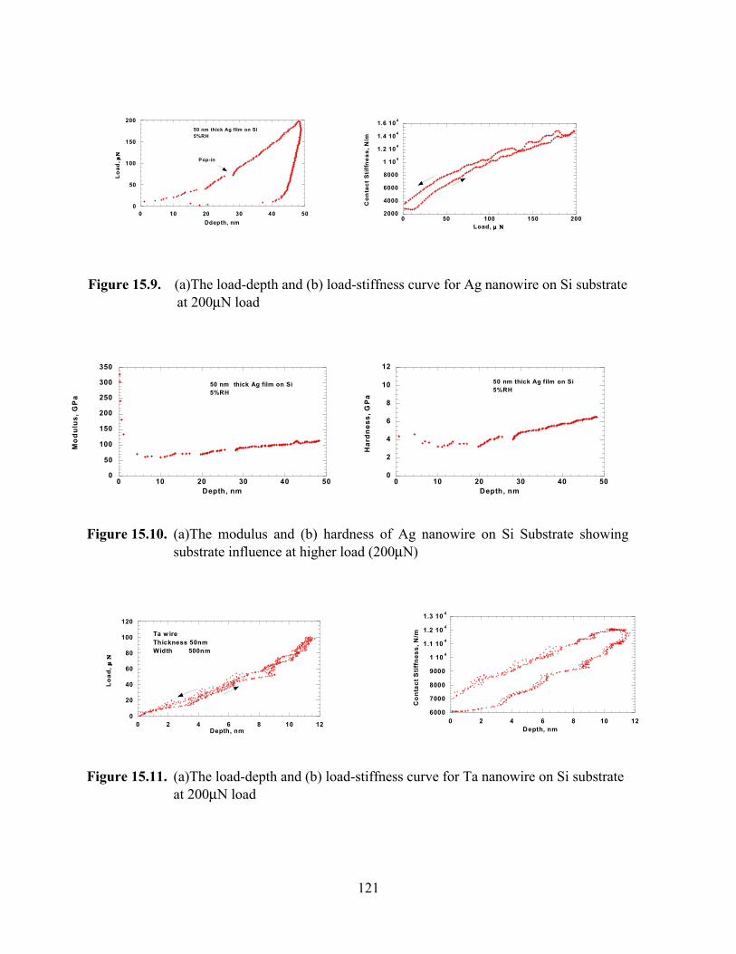
121
Figure 15.9. (a)The load-depth and (b) load-stiffness curve for Ag nanowire on Si substrate at 200µN load
Figure 15.10. (a)The modulus and (b) hardness of Ag nanowire on Si Substrate showing
substrate influence at higher load (200µN)
Figure 15.11. (a)The load-depth and (b) load-stiffness curve for Ta nanowire on Si substrate
at 200µN load
0
20
40
60
80
100
120
0 2 4 6 8 10 12
Load
, µµ µµ
ΝΝ ΝΝ
Depth, nm
Ta w ireThickness 50nmWidth 500nm
0
50
100
150
200
0 10 20 30 40 50
Load
, µΝ
µΝ
µΝ
µΝ
Ddepth, nm
50 nm thick Ag film on Si5%RH
Pop-in
2000
4000
6000
8000
1 104
1.2 104
1.4 104
1.6 104
0 50 100 150 200
Con
tact
Stif
fnes
s, N
/m
Load, µµµµ
ΝΝΝΝ
0
50
100
150
200
250
300
350
0 10 20 30 40 50
Mo
dulu
s, G
Pa
Depth, nm
50 nm thick Ag film on Si5%RH
0
2
4
6
8
10
12
0 10 20 30 40 50
Har
dnes
s, G
Pa
Depth, nm
50 nm thick Ag film on Si5%RH
6000
7000
8000
9000
1 10 4
1.1 10 4
1.2 10 4
1.3 10 4
0 2 4 6 8 10 12
Con
tact
Stif
fnes
s, N
/m
Depth, nm

122
Figure 15.12. (a) The modulus and (b) hardness of Ta nanowire on Si Substrate showing
substrate influence at shallower depths
16. "Size Effects in Magnetic and Superconducting Materials"
(Ivan K. Schuller)
Summary of Research
We have developed the technology for the fabrication of nanostructures by several
different methods: electron beam, diblock copolymer, and self assembly. The electron beam
lithography technique has been used to prepare a large number of different structures for
studies of flux pinning in superconductors and for investigations of magnetic hysteresis.
Flux pinning has been extensively studied in a variety of geometrical arrangements of
magnetic dots. In particular, square arrays of dots allow for the first time investigation of the
pinning mechanism. At present, there are several experiments under way which will give a
direct measure of the pinning energy for various magnetic materials and in different magnetic
states (i.e. single or multi domain). Interestingly these experiments also give information on
the magnetic state of the dots, which is being used to investigate purely magnetic
phenomena. Many of these measurements and techniques were developed and performed in
collaboration with Prof. Sharifi's group.
0
100
200
300
400
0 2 4 6 8 10 12
Mod
ulus
, GP
a
Depth, nm
Ta wire Thickness 50 nmWidth 500 nm
0
5
10
15
20
25
0 2 4 6 8 10 12
Har
dnes
s, G
Pa
Depth, nm

123
In collaboration with Profs. S. von Molnar, and S. Pearton we are currently
investigating exchange bias in bilayers of an antiferromagnet (FeF2, initially) and a
nanostructured ferromagnet (Fe, initially). Bilayered films and the electron beam lithography
is performed in Prof. Schuller's laboratory, selective height lithography is done using
techniques developed by Prof. Pearton and collaborators, and measurements using a novel
2D electron gas Hall probe is performed by Prof. von Molnar. We found that
nanostructuring the ferromagnet changes the exchange bias and hysteresis behavior of the
ferromagnetic film. This has important implications for applications in the field of magnetic
sensors and memories which invariably use exchange bias as an integral part of the device.
In collaboration with Prof. S. Hershfield, we are performing a theoretical-
experimental study of the anisotropic magnetotransport in magnetic superlattices (Fe/Cr
initially). We have performed extensive studies of the structure, magnetic and
magnetotransport properties of Fe/Cr superlattices in a large variety of configurations and for
different preparation methods. A particularly unique capability in our lab is the measurement
of the perpendicular resistivity (i.e. with the current perpendicular to the interfaces). This
measurement is more amenable to theoretical calculations. In addition, together with our
quantitative studies, this is probably the most complete study on the interconnection between
structure and magnetotransport in metallic superlattices. In this fashion, we are able to obtain
quantitative data of structural parameters such as roughness, interdiffusion, length scales,
resistivity, magnetoresistance, magnetization, etc. These can be then fed into theoretical
models and obtain quantitative results regarding microscopic parameters.

124
17. Theory of GMR
(Selman Hershfield)
Last year we successfully completed calculations of the CPP GMR in materials like
FeCr. These calculations included realistic electronic structure and different kinds of
scattering - both surface and bulk. This theory compared well with experiments done on the
CPP GMR so we are confident that it is an accurate description.
In this, the final year of this project we wish to carry these calculations to the next
level and use the theoretical model to try optimize the experimental parameters and produce
the maximum possible GMR. This is the so-called inverse band-structure problem of finding
an atomic configuration with given electronic properties (see Franceschetti and Zunger,
Nature 402, 60 (1999).) For our case the desired electronic property is the maximum possible
GMR.
My senior graduate student on this project, Tat-Sang Choy, is in the process of
optimizing our GMR code so that many different runs can be done. Each run contains a
slightly different configuration and an optimization technique called simulated annealing is
used to choose the next atomic configuration. Note that simulated annealing as an
optimization tool and should not be confused with real physical annealing.
Tat-Sang Choy has already improved the running speed of the code by several orders
of magnitude so that what used to take a day to run now only takes minutes. The
developments he has made have been well documented and will form the major part of his
thesis so we should be able to transfer this knowledge effectively to others in the field.

125
18. Ion Beam Sputter Deposition of GMR Materials
(D. Temple)
I. Summary
MCNC's Role in the Program
During the second phase of the MURI program (years 4 and 5), the statement of work for
MCNC, a subcontractor to the University of Florida, included two major tasks:
1. Development of ion beam sputter deposition (IBSD) techniques for deposition of GMR
multilayers, using the IBSD system designed, constructed, and automated in-house.
2. Device processing and photolithographic mask/design and fabrication support for other
organizations in the MURI program.
Progress During the Last Reporting Period
Task 1:
• Demonstrated deposition of polycrystalline Fe/Cr multilayers exhibiting the GMR effect,
with GMR ratios comparable to the best ones obtained by RF sputtering.
• Examined effects of variations of the primary ion beam energy and the type of ions on GMR
values; the investigated primary ion energy range was 700 eV- 1200 eV for Ar ions and 900
eV - 1200 eV for Xe ions. Demonstrated that the GMR ratio is greater for films deposited
using Xe ions than for films deposited using Ar ions, and that for both types of ions the GMR
ratio increases as the primary ion beam energy decreases.
• Modeled the observed dependence of the GMR ratio on the primary ion beam energy value
and the type of ions via a correlation of the measured GMR values with the average energy
transferred to the substrate during the film growth. This energy was calculated using the
Transport of Ions in Matter (TRIM) algorithm based on the Monte Carlo method.
• Modified the configuration of the IBSD equipment to expand the range of primary ion beam
energies to include lower deposition energies, potentially optimizing GMR ratios of the Fe/Cr
multilayer system. These modifications included: a) changes in the vacuum pumping system
126
to provide lower base and operating pressures as well as shorter pumping and pump
regeneration cycles; b) a rebuild of the ion gun consisting of the replacement of the quartz
chamber and installation of curved accelerator grids designed to reduce the ion beam
spreading; and c) the installation of magnetic sensors to monitor the position of metal targets
as they rotate into place during the deposition of multilayers.
Task 2:
• A series of Si/SiO2/metal capacitors were fabricated for studies of the screening length of thin
magnetic films; the studies were conducted in Art Hebard's group at the University of
Florida.
• Magnetic metal multilayer electrodes were fabricated for spin field-effect transistor studies;
the studies were conducted in Fen Ren's group at the University of Florida.
• Three sets of photolithographic masks were designed and fabricated for the University of
Florida, Florida State University and University of California in San Diego.
II. Detailed Description - Ion Beam Sputter Deposition Development
Effect of Processing Parameters on Magnetic Properties of Fe/Cr Multilayers
The configuration of the IBSD system has been described in detail in progress report #4.
For this study, we have deposited the following Fe/Cr multilayer combinations:
Si/Cr(50Å)/[Fe(20Å)/ Cr(t(Å))]x30/Cr(50Å- t(Å)), where t was varied from 8 to 14 Å; this range
surrounds the first antiferromagnetic maximum in the Fe/Cr multilayer system. The deposition
rates varied from 5 to 30 Å/min depending on the primary ion beam energy, the type of ions, and
the target material. The films were deposited at room temperature.
Deposited multilayers were characterized using Transmission Electron Microscopy
(TEM), Atomic Force Microscopy (AFM), Auger Electron Spectroscopy (AES), X-ray
Photoelectron Spectroscopy (XPS) as well as resistivity, magnetic hysteresis loop and
magnetotransport measurements. Film resistivity was determined from sheet resistance values
obtained using a four-point probe. Magnetic hysteresis loop measurements were performed
using a vibrating sample magnetometer (VSM). Magnetotransport measurements were obtained

127
at the University of Florida (in the group of Dr. Arthur Hebard, one of the investigators in the
MURI program) using two different instruments. The first of these, a Physical Properties
Measurement System (PPMS, Quantum Design) allows measurements as a function of
temperature (2-400K), magnetic field (0-7T), and angle (0-360 degrees). The second instrument,
a Magnetic Properties Measurement System (MPMS, Quantum Design), can also be used for
magnetoresistance measurements. Its temperature and field ranges are similar to those of the
PPMS.
Among other structural measurements, low angle X-ray diffraction (XRD) was performed
on selected films to verify the composition of the multilayers. As an example, Figure 1 shows a
low angle XRD spectrum for a film with a nominal composition of
Si/Cr(50Å)/[Fe(20Å)/Cr(10Å))]x30/Cr(40Å), obtained using a BEDE D3 diffractometer using
Cu radiation from a rotating anode source operating at 40 kV and 120 mA. The scan was run
from 0 to 16,000 arcsec with a stepsize of 25 arcsec and a counting time of 30 sec/step. The
structural parameters, such as density, thickness and roughness, were fit using a commercially
available autofit algorithm (BEDE Mercury REFS). All parameters were allowed to vary
independently. The only constraint was that the roughness for a layer could not be greater than
the nominal thickness of that layer. The fit resulted in the value of 30 Å for the modulation
period, in perfect agreement with the nominal value, and in the average interface roughness value
of 5 Å.
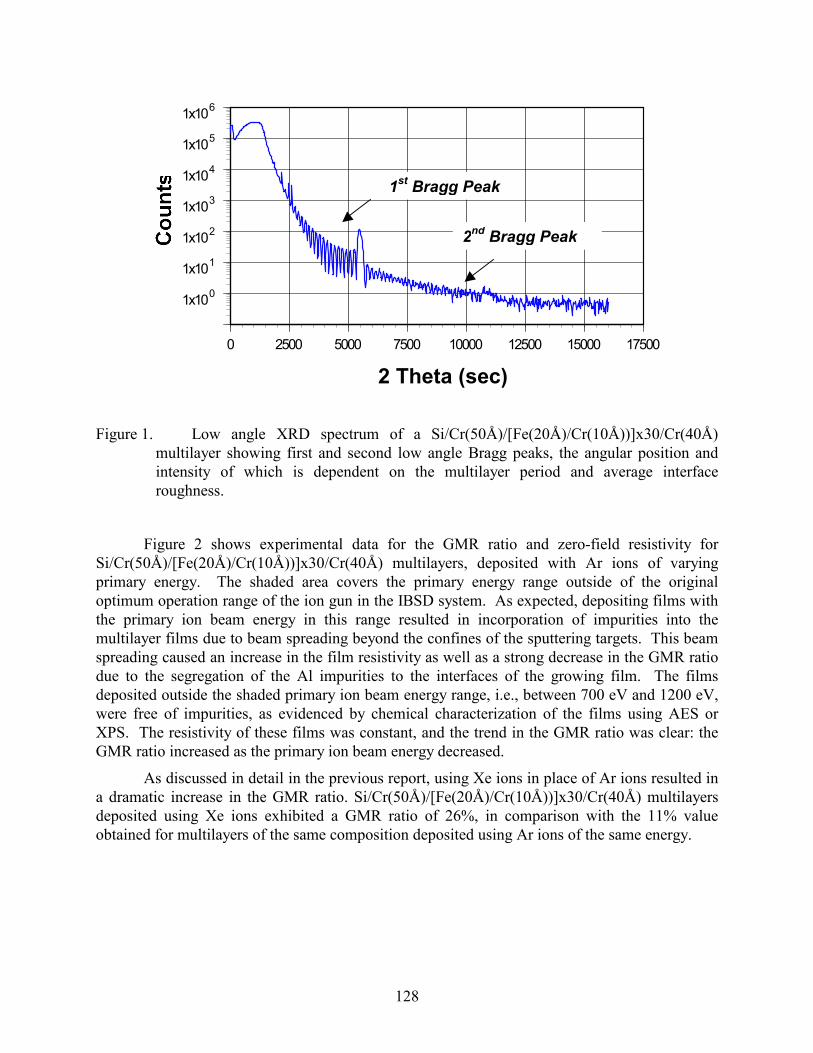
128
1x10⁻¹
1x100
1x101
1x10²
1x10³
1x10⁴
1x10⁵
1x10⁶
0 2500 5000 7500 10000 12500 15000 17500
2 Theta (sec)
Figure 1. Low angle XRD spectrum of a Si/Cr(50Å)/[Fe(20Å)/Cr(10Å))]x30/Cr(40Å) multilayer showing first and second low angle Bragg peaks, the angular position and intensity of which is dependent on the multilayer period and average interface roughness.
Figure 2 shows experimental data for the GMR ratio and zero-field resistivity for Si/Cr(50Å)/[Fe(20Å)/Cr(10Å))]x30/Cr(40Å) multilayers, deposited with Ar ions of varying primary energy. The shaded area covers the primary energy range outside of the original optimum operation range of the ion gun in the IBSD system. As expected, depositing films with the primary ion beam energy in this range resulted in incorporation of impurities into the multilayer films due to beam spreading beyond the confines of the sputtering targets. This beam spreading caused an increase in the film resistivity as well as a strong decrease in the GMR ratio due to the segregation of the Al impurities to the interfaces of the growing film. The films deposited outside the shaded primary ion beam energy range, i.e., between 700 eV and 1200 eV, were free of impurities, as evidenced by chemical characterization of the films using AES or XPS. The resistivity of these films was constant, and the trend in the GMR ratio was clear: the GMR ratio increased as the primary ion beam energy decreased.
As discussed in detail in the previous report, using Xe ions in place of Ar ions resulted in a dramatic increase in the GMR ratio. Si/Cr(50Å)/[Fe(20Å)/Cr(10Å))]x30/Cr(40Å) multilayers deposited using Xe ions exhibited a GMR ratio of 26%, in comparison with the 11% value obtained for multilayers of the same composition deposited using Ar ions of the same energy.
1st Bragg Peak
2nd Bragg Peak

129
0
2
4
6
8
10
12
0 200 400 600 800 1000 1200
Primary Ion Beam Energy (eV)
GM
R (%
)
0.0E+0
2.0E-5
4.0E-5
6.0E-5
8.0E-5
1.0E-4
1.2E-4
Res
istiv
ity (o
hm c
m)
Si/Cr(50A)/[Fe(20A)/Cr(12A)]x30/Cr(38A) Ar ion beam
Figure 2. GMR ratio and zero-field resistivity for Fe/Cr multilayers deposited using Ar ions with
varying primary ion beam energy. The shaded area corresponds to the "forbidden" energy range for the then-current configuration of the ion gun.
The fact that the GMR ratio is dependent on both the type of ions as well as on the primary ion beam energy points to a possible correlation between the GMR values and energies of species arriving at the substrate. These energetic species include sputtered atoms and reflected neutrals resulting from neutralization of the primary ion beam as it approaches the sputtering target. To explore this correlation, we have calculated energy distributions for sputtered Fe and Cr atoms, as well as for the reflected neutrals. The energy distributions vary as functions of the type of primary ions and the primary energy of the ions. These calculations were performed using a commercial algorithm (Transport of Ions in Matter, TRIM) based on the Monte Carlo method. Based on the energy distributions, we have calculated the average energy per sputtered atom deposited onto the substrate during the multilayer growth. Figure 3 presents a plot of the measured GMR ratio for the Fe/Cr multilayers as a function of the calculated average energy per atom. As can be seen from the figure, as the average energy increases, the GMR ratio decreases. This result can be attributed to the increased probability of creating defects that form non-spin-

130
dependent scattering centers, and the increased degree of intermixing at interfaces associated with an increase of an average energy per atom.
05
1015202530
10 15 20 25 30
Calculated Average Energy Per Atom (eV/atom)
GM
R ra
tio (%
)
Figure 3. Correlation between experimentally determined GMR ratios for
Si/Cr(50Å)/[Fe(20Å)/Cr(10Å))]x30/Cr(38Å) multilayers and calculated values of the average energy per sputtered atom deposited into the substrate during the multilayer growth. This energy is a function of the type of ions and the primary ion beam energy.
II2. IBSD System Modifications
The necessary modifications of the IBSD system performed during the reporting period included changes in the vacuum pumping system to provide lower base and operating pressures as well as shorter pumping and pump regeneration cycles. Figure 4 shows a schematic diagram of the IBSD system before and after the modifications performed on the pumping configuration. The "before" configuration relied on the roughing pump to achieve a pressure of about 300 mTorr in the deposition chamber. At that point in the pumpdown sequence, the gate valve isolating the roughing pump from the rest of the system was closed, and the pressure in the chamber was decreased further using a cryogenic pump. This cryopump was responsible for reaching and maintaining ultra-high vacuum (UHV) before and after deposition, as well as maintaining a pressure in the 10-4 Torr range during the deposition. Since the cryopump was not isolated from the rest of the system in the "before" configuration, the regeneration of the pump, a part of the routine maintenance, required a shutdown of the system. When Xe is used as the source gas, the regeneration of the cryopump must be done frequently, because Xe is susceptible to freezing on the entry baffle of the pump, inhibiting its pumping efficiency.

131
Figure 4. Schematic diagrams for the IBSD system before and after the modification.
Chamber
Cryo pump
Sample Intro
“Small” Turbo
Load Rod
Roughing Pump
Diaphragm Pump
Isolation Valve
BEFORE
AFTER
Chamber
Cryo pump
Sample Intro
“Small” Turbo
Load Rod
Roughing Pump
Diaphragm Pump
GateValv
e
(future
“Large” Turbo 500 L/sec
Roughing Pump
53 L/sec
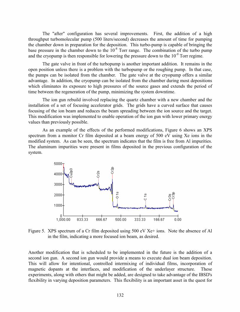
132
The "after" configuration has several improvements. First, the addition of a high throughput turbomolecular pump (500 liters/second) decreases the amount of time for pumping the chamber down in preparation for the deposition. This turbo-pump is capable of bringing the base pressure in the chamber down to the 10-8 Torr range. The combination of the turbo pump and the cryopump is then responsible for lowering the pressure down to the 10-9 Torr regime.
The gate valve in front of the turbopump is another important addition. It remains in the open position unless there is a problem with the turbopump or the roughing pump. In that case, the pumps can be isolated from the chamber. The gate valve at the cryopump offers a similar advantage. In addition, the cryopump can be isolated from the chamber during most depositions which eliminates its exposure to high pressures of the source gases and extends the period of time between the regeneration of the pump, minimizing the system downtime.
The ion gun rebuild involved replacing the quartz chamber with a new chamber and the installation of a set of focusing accelerator grids. The grids have a curved surface that causes focusing of the ion beam and reduces the beam spreading between the ion source and the target. This modification was implemented to enable operation of the ion gun with lower primary energy values than previously possible.
As an example of the effects of the performed modifications, Figure 6 shows an XPS spectrum from a monitor Cr film deposited at a beam energy of 500 eV using Xe ions in the modified system. As can be seen, the spectrum indicates that the film is free from Al impurities. The aluminum impurities were present in films deposited in the previous configuration of the system.
Figure 5. XPS spectrum of a Cr film deposited using 500 eV Xe+ ions. Note the absence of Al
in the film, indicating a more focused ion beam, as desired.
Another modification that is scheduled to be implemented in the future is the addition of a second ion gun. A second ion gun would provide a means to execute dual ion beam deposition. This will allow for intentional, controlled intermixing of individual films, incorporation of magnetic dopants at the interfaces, and modification of the underlayer structure. These experiments, along with others that might be added, are designed to take advantage of the IBSD's flexibility in varying deposition parameters. This flexibility is an important asset in the quest for

133
a greater understanding of the mechanisms involved in the GMR effect. Another modification that will enhance the capabilities of the current IBSD system is the installation of the shutter assembly. The electrically actuated shutter will protect the substrate during the initial beam current rise time, as well as during precleaning of the targets.
III. Plans For the Remainder of the Program
• Continue investigations of the effect of the primary ion beam energy on magnetoresistive properties of Fe/Cr multilayers using the extended ion beam energy range made possible by the recent system modifications.
• Optimize the GMR ratio for Co/Cu multilayers and/or spin valves as a function of IBSD deposition conditions. Correlate the GMR values with the average energy metric to arrive at material-specific, but deposition-system-independent process condition windows.
• Continue to support University of Florida and other participating institutions by providing wafers with high resolution liftoff patterns for patterning of magnetic multilayers, performing TEM analyses of deposited materials, designing masks/reticles for use in photolithographic processes and providing device fabrication services.
• Optimize processes for formation of contacts to patterned magnetic multilayers using single and dual level metallization schemes.
134
Technology Transitions
1. Ultra-high density patterning process (> 64 Mbit·in-2) based on e-beam lithography for
future generations of rad-hard, infinitely rewritable Magnetic Random Access Memories (MRAMs) – work done in collaboration with Honeywell Solid State Technology Center, MN.
2. Growth of high quality CoFeB and low temperature NiMnSb thin films (< 250oC), both of which are attractive candidates for next generation information storage devices – work done in collaboration with IBM Almaden Research Center, San Jose, CA.
3. Development of the non-corrosive Co/NH3 plasma chemistry for shallow feature etching (e.g. MRAMs) – work done in conjunction with Plasma-Therm, St. Petersburg, FL and Seagate, MN.
4. Development of new Kerr probe for ultra-high B field magneto-optical measurements – work done in conjunction with National High Magnetic Field Laboratory, Tallahassee, FL, where the probe is available as a user facility.
5. Maskless approaches to ultra-high density patterning for future generations of rad-hard, infinitely rewritable Magnetic Random Access Memories (MRAMs) – work initiated in collaboration with Honeywell Solid State Technology Center, MN.
6. Discovered a dry etching process for NiFe and related alloys based on a balance between chemical surface reaction with Cl, and ion-assisted desorption of the reaction products, followed by in-situ removal of Chlorine resides to prevent corrosion. This is being transitioned to Honeywell for use in fabricating high density, rad-hard, non-volatile magnetic Random Access Memories (MRAMs).
7. Growth of the first high quality, potentially 100% spin-polarized NiMnSb thin films at low (250oC) temperatures. These are attractive candidates for advanced magnetic storage devices with improved Giant Magneto-Resistance response.
8. Development of techniques for reducing the ultimate limits of e-beam lithography, and resultant achievement of individual features with dimension < 300Å, and dense arrays (> 10 Gbits·in-2) of 500Å features for next generation information storage devices.
9. Growth of improved nanoscale SrS:Ce, F thin films which emit in the blue, using addition of GaS during rf-magnetron deposition. These have application for full color electroluminescent displays. A plasma etching process for patterning of these films has also been discovered (work done in collaboration with Planar Systems, the only domestic supplier of EL displays).

135
Interactions and Industrial Contacts 1. IBM Almaden Research Center, San Jose, CA – new nanoscale materials and processes
for computer hard devices 2. Honeywell Solid State Electronics Center, Plymouth, MN – new processes for radiation-
hard memory. 3. Honeywell Space Systems, Clearwater, FL – next generation MRAM for use in
submarine-based missile systems. 4. Plasma-Therm, St. Petersburg, FL – new etch processes for magnetic materials. 5. Seagate, Minneapolis, MN – new etch processes for magnetic material. 6. IBM T.J. Watson Research Center, Yorktown heights, NY - new etch processes for
magnetic materials. 7. Motorola, Tempe, AZ – advanced processing for MRAM. 8. Bell Laboratories, Lucent Technologies – deposition/etching of advanced dielectrics for
memory devices. 9. Piezo Technology, Inc., Orlando, FL – characterization/etching of new oxides for ultra-
precise timing applications (oscillators). 10. Corning, Corning, NY – advanced dielectrics for magnetic sensors. 11. Naval Research Laboratory, Washington, DC – methods for measuring mechanical
properties at the nanoscale, and fabrication of spin-FETs. 12. Sandia National labs, Albuquerque, NM – high rate etching processes for magnetic
multilayers. 13. Allied Signal, Columbia, MD – e-beam lithography for ultra-dense patterning. 14. American Crystal Technology, Fremont, CA – growth of dilute magnetic semiconductors. 15. US Army Research Lab, Adelphi, MD – magnetic sensors.

136
Publications “Large Magnetic Entropy in GMR a-Gdx Si1=x,” B. Zink, E. Junard, K. Allen and F. hellman, Phy. Rev. Lett. 83, 2266 (1999). “Low Temperature MR in Insulating a-Gdx Si1-x Alloys,” P Xiong, B.L. Zink, S. Apllebaum and F. Hellman, Phys. Rev. B59, 3929 (1999). “Parametric Study of NiFe and NiFeCo High Density Plasma Etching Using CO/NH3,” K.B. Jung, H. Hong, H. Cho, S. Onishi, D. Johnson, Y.D. J.R. Childress and S.J. Pearton, J. Electrochem. Soc. 146, 2163 (1999). “ICP Etching of CoFeB, CoZr, CoSm and FeMn Thin Films in Interhalogen Mixtures,” H. Cho, K.B. Jung, D.C. Hays, Y.B. Hahn, T. Feng, Y.D. Park, J.R. Childress, F.J. Cadieu, R. Rami, X.R. Qian, L. Chen and S.J. Pearton, Mat. Sci. Eng. B60, 107 (1999). “Cl2-based ICP Etching of CoFeB, CoSm, CoZr and FeMn,” K.B. Jung, H. Cho, Y.B. Hahn, D.C. Hays, T. Feng, Y.D. Park, J.R. Childress and S.J. Pearton, Mat. Sci. Eng. B60, 101 (1999). “Selective Dry Etching using ICP, Part I: GaAs/AlGaAs and GaAs/InGaP,” D.C. Hays, H. Cho, K.B. Jung, Y.B. Hahn, C.R. Abernathy, S.J. Pearton, F. Ren and W.S. Hobson, Appl. Surf. Sci. 147, 125 (1999). “Selective Dry Etching using ICP, Part II: InN/GaN and InN/AlN,” D.C. Hays, H. Cho, K.B. Jung, Y.B. Hahn, C.R. Abernathy, S.J. Pearton, F. Ren, J. Han and R.J. Shul, Appl. Surf. Sci. 147, 134 (1999). “Effect of Inert Gas Additive Species on Cl2 High Density Plasma Etching of Compound Semiconductors Part I: GaAs and GaSb,” Y.B. Hahn, D.C. Hays, H. Cho, K.B. Jung, C.R. Abernathy, S.J. Pearton and R.J. Shul, Appl. Surf. Sci. 147, 207 (1999). “Effect of Inert Gas Additive Species on Cl2 High Density Plasma Etching of Compound Semiconductors Part II: InP, InSb, InGaP and InGaAs,” Y.B. Hahn, D.C. Hays, H. Cho, K.B. Jung, C.R. Abernathy, S.J. Pearton and R.J. Shul, Appl. Surf. Sci. 147, 215 (1999). “Comparison of Cl2 and F2 based Chemistries for the ICP Etching of NiMnSb Thin Films,” J. Hong, J. Caballero, E.S. Lambers, J.R. Childress and S.J. Pearton, J. Vac. Sci. Technol. A17, 1326 (1999). “Damage to III-V Devices During ECR-CVD,” J.W. Lee, K. MacKenzie, D. Johnson, R.J. Shul, Y. Hahn, D.C. Hays, C.R. Abernathy, F. Ren and S.J. Pearton, J. Vac. Sci. Technol. A17, 2183 (1999).
137
“Effect of Inert Gas Additive on Cl2-based ICP Etching of NiFe and NiFeCo,” K.B. Jung, H. Cho, Y.B. Hahn, D.C. hays, E.S. Lambers, Y.D. Park, T. Feng, J.R. Childress and S.J. Pearton, J. Vac. Sci. Technol. A17, 2223 (1999). “Study of ICP NH3 Plasma Damage on GaAs Schottky Diodes,” L.C. Meyer, J.W. Lee, D. Johnson, M. Huang, F. Ren, T.J. Anderson, J.R. LaRoche, J.R. Lothian, C.R. Abernathy and S.J. Pearton, J. Electrochem. Soc. 146, 2717 (1999). “Cl2-based Dry Etching of Doped Manganate Perovskites: PrBaCaMnO3 and LaSrMnO3,” K.P. Lee, K.B. Jung, H. Cho, D. Kumar, S.V. Pietambaram, R.K. Singh, P.H. Hogan, K.H. Dahmen, J.B. Hahn and S.J. Pearton, J. Electrochem. Soc. 146, 2748 (1999). “Novel In-Situ Ion Bombardment Process for a Thermally Stable (7800oC) Plasma Deposited Dielectric,” Electrochemical and Solid-State Letters 2, 537, (1999). “Dry Etching of BaSrTiO3 and LaNiO3 Thin Films in Inductively Coupled Plasmas,” K.P. Lee, K.B. Jung, A. Srivastava, D. Kumar, R.K. Singh and S.J. Pearton, J. Electrochem. Soc. 146, 3778 (1999). “Inductively Coupled Plasma Etching of Ta2O5,” K.P. Lee, K.B. Jung, R.K. Singh, S.J. Pearton, C. Hobbs and P. Tobin, J. Electrochem. Soc. 146, 3794 (1999). “Mechanism of High Density Plasma Etch Processes for Ion-driven Etching of Materials,” J.W. Lee, J.F. Donahue, K.D. MacKenzie, R. Westerman, D. Johnson and S.J. Pearton, Solid-State Electron. 43, 1769 (1999). “Fabrication and Magneto-transport and SQUID Measurements of Sub-micron Spin-valve Structures,” Y.D. park, D. Temple, K.B. Jung, D. Kumar, P.H. Holloway and S.J. Pearton, J. Vac. Sci. Technol. B17, 2471 (1999). “Development of Chemically-assisted Dry Etching Methods for Magnetic Device Structures,” K.B. Jung, H. Cho, K.P. Lee, J. Marburger, F. Sharifi, R.K. Singh, D. Kumar, K.H. Dahmen and S.J. Pearton, J. Vac. Sci. Technol. B17, 3186 (1999). “Plasma Etching of Magnetic Multilayers-effect of Concurrent UV Illumination,” H. Cho, K.P. Lee, Y.B. Hahn, E.S. Lambers and S.J. Pearton, Mat. Sci. Eng. B67, 145 (1999). “Long-term Stability of Dry Etched MRAM Elements,” K.B. Jung, J. Marburger, F. Sharifi, Y.D. Park, E.S. Lambers and S.J. Pearton, J. Vac. Sci. Technol. A18, 268 (2000). “Dry Etch Selectivity of Gd2O3 to GaN and AlN,” D. Hays, K.P. Lee, B.P. Gila, F. Ren, C.R. Abernathy and S.J. Pearton, J. Electron. Mater. 29, 285 (2000).

138
“Comparative Study of Ni Nanowires Patterned by e-beam Lithography and Fabricated by Life-off and Dry Etching Techniques,” Y. Park, K.B. Jung, M. Overberg, D. Temple, S.J. Pearton and P.H. Holloway, J. Vac. Sci. Technol. B18, 16 (2000). “Thermal Stability and Etching Characteristics of e-beam Deposited SiO and SiO2,” J. LaRoche, F. Ren, J. Lothian, J. Hong, S.J. Pearton, E. Lambers, C.H. Chu, C.S. Wu and M. Hoppe, J. Vac. Sci. Technol. B18, 283 (2000). “Ultraviolet Light Enhancement of Ta2O5 Dry Etch Rates,” K.P. Lee, H. Cho, R.K. Singh, S.J. Pearton, C. Hobbs and P. Tobin, J. Vac. Sci. Technol. B18, 293 (2000). “Effect of UV Illumination on SiC Dry Etch Rates,” P. Leerungnawarat, H. Cho, S.J. Pearton, C.-M. Zetterling and M. Östling, J. Electron. Mater. 29, 342 (2000). “Low Temperature SiNx and SiO2 Film Processing by ICP-CVD,” J.W. Lee, K.D. MacKenzie, D. Johnson, J.N. Sasserath, S.J. Pearton and F. Ren, J. Electrochem. Soc. 147, 1481 (2000). "Magnetization Behavior of Nanometer-scale Iron Particles," S. Wirth, M. Field, D. D. Awschalom and S. von Molnár, Phys. Rev. B 57 (1998), R 14028-14031. "Magnetism of Nanometer-scale Iron Particle Arrays, " S. Wirth, M. Field, D. D. Awschalom and S. von Molnár, J. Appl. Phys. 85 (1999), pp.5249-5254. "Magnetic Interactions In Nanometer-Scale Particle Arrays Grown Onto Permalloy Films," S. Wirth and S. von Molnár presented at MMM'99, J. Appl. Phys. 87 (2000) pp.7010-7012. "Thermally Activated Magnetization Reversal In Nanometer-Size Iron Particles," S. Wirth, A. Anane and S. von Molnár (to be published). “Synthesis and Characterization of Silica-Coated Iron Oxide Nanoparticles in Microemulsion: The Effect of Non-Ionic Surfactants,” S. Santra, R. Tapec, N. Theodoropoulou, A. F. Hebard, W. Tan, submitted to Langmuir (6/20/2000). “Superparamagnetism in Discontinuous Ni Films,” A. Frydman, T. Kirk and R.C. Dynes, Solid State Communication 114, 481 (2000). “Magnetoresistance of Granular Ferromagnets - Observation of a Magnetic Proximity Effect,” A. Frydman and R.C. Dynes, Solid State Communications 110, 485 (1999). ‘Superconducting Tunneling as a Probe of Sputtered Oxide Barriers,” C.L. Platt, A.S. Katz, R.C. Dynes and A.E. Berkowitz, Appl. Phys. Lett. 75, 127 (1999). “Disorder-induced Andreev Reflections in Granular Metals,” A. Frydman and R.C. Dynes, Phys. Rev. B 59, 8432 (1999).

139
“Superconducting and Spin-Dependent Tunneling Using Native Oxide Barriers on Co-Fe Thin Films,” C.L. Platt, A.S. Katz, E.P. Price and R.C. Dynes, Phys. Rev. B 61, 68 (2000). “Nanoscale Surface Mechanical Property Measurements: Force Modulation Techniques Applied to Nanoindentation,” S.A.S. Asif, R.J. Colton, and K.J. Wahl, accepted for publication in Interfacial Properties on the Submicron Scale, R. Overney and J. Frommer, eds., ACS/Oxford Press, Jan. 2000. “Quantitative Study of Nanoscale Contact and Pre-Contact Mechanics Using Force Modulation,” S.A.S. Asif, K.J. Wahl, and R.J. Colton, Thin Films: Stresses and Mechanical Properties VIII, , R. Vinci, O. Kraft, N. Moody, P. Besser, E. Shaffer II, eds., Vol. 594 (Materials Research Society, Warrendale, PA, 2000). “The Influence of Oxide and Adsorbates on the Nanomechanical Response of Silicon Surfaces,” S.A. Syed Asif, K.J. Wahl, and R.J. Colton, J. Mater. Res. 15 (2000) 546-553. “Nanoindentation – Quantitative Study of the Nanomechanical Properties of Materials Using Depth Sensing and Force Modulation,” S.A. Syed Asif, K.J. Wahl, O. Warren, and R.J. Colton, to be published in “SXM Industrial Use,” R.J. Colton and H. Fuchs, Eds. (Springer Verlag, submitted).
"Suppression of Growth-Induced Perpendicular Magnetic Anisotropy in Co-Pt Alloys by Trace Amounts of Si", A. L. Shapiro, O. Vajk, B. M. Maranville, and F. Hellman, Appl. Phys. Lett. 75, 4177 (1999). "Growth-Induced Perpendicular Anisotropy and Clustering in NixPt1-x alloys.” A. L. Shapiro, D. Vasumathi, B. M. Maranville, and F. Hellman, paper submitted to J. Magn. Magn. Mat. (2000). "Growth-Induced Anisotropy on Vicinal Substrates,” B. M. Maranville, A. L. Shapiro, D. Vasumathi, and F. Hellman, paper in preparation, to be submitted to J. Appl. Phys. (2000). “Ion-Beam Assisted Growth of Perpendicular Anisotropy Materials, “D. Vasumathi, B. M. Maranville, and F. Hellman, paper in preparation, to be submitted to J. Appl. Phys. (2000). “Magnetic and Thermodynamic Features Of Antiferromagnetic Nanoparticles In A Metallic Matrix,” R. Sappey, E. P. Price, F. Hellman, A. E. Berkowitz, and D. J. Smith, in preparation; to be submitted to Physical Review. “Oxygen Content and Crystallinity Effects in Pulsed Laser Deposited Lanthanum Manganite Thin Films,” Srinivas V. Pietambaram, D. Kumar, Rajiv K. Singh, and C. B. Lee, Proceedings of the 2000 MRS Spring Meeting, San Francisco, CA, USA “Artificially Induced Reconfiguration of the Vortex Lattice by Arrays of Magnetic Dots,” Jose Martin, M. Velez, A. Hoffmann, Ivan K. Schuller, and J.I. Vicent, Phys. Rev. Lett. 83, 1022 (1999).
140
“Periodic Vortex Pinning with Magnetic and Non-Magnetic Dots: Does the Size Matter?,” A. Hoffmann, P. Prieto, and Ivan K. Schuller Phys. Rev. B 61, 6958 (2000). “Metallic Superlattices,” Ivan K. Schuller, Physics Today – Invited Article (To appear, 2000). "Processing Techniques for InGaAs/InAlAs/InGaAs Spin Field Effect Transistors," J.R. LaRoche, F. Ren, D. Temple, S.J. Pearton, J.M. Kuo, A.G. Baca, P. Cheng, Y.D. Park, Q. Hudspeth, A.F. Hebard, and S.B. Arnason, to be published in Solid State Electronics (2000). "Comparative Study of Ni Nanowires Patterned by E-Beam Lithography and Fabricated by Lift-off and Dry Etching Techniques," Y.D. Park, K.B. Jung, M. Overberg, D. Temple, S.J. Pearton and P.H. Holloway, J. Vac. Sci. Technol. B18 (2000) 16. "Fabrication and Magneto-Transport and SQUID Measurements of Sub-Micron Spin-Valve Structures," Y.D. Park, D. Temple, K.B. Jung, D. Kumar, P.H. Holloway, and S.J. Pearton, J. Vac. Sci. Technol. B17 (1999) 2471.
141
Technical Presentations “Electrical Noise from Phase Separation in PrCaMnO3 Single Crystal,” A. Prange, S. von Molnar, L. Pinsaid-Godast and A. Revcolevschi, 44th Ann. Conf. Magnetism and Magnetic Materials, San Jose, November 1999. “Magnetic Interactions in nm-Scale Particle Arrays Grown onto Permalloy Films,” S. Wirth and S. con Molnar, 44th Ann. Conf. Magnetism and Magnetic Materials, San Jose, November 1999. “Investigating Artificial Barriers in Spin-Dependent Tunnel Junctions with Superconducting Electrodes,” C. Platt, A. Berkowitz, A.S. Katz and R.C. Dynes, 44th Ann. Conf. Magnetism and Magnetic Materials, San Jose, November 1999. “Anisotropic Magnetotransport and Microstructural Analysis of Fe/Cr Superlattices,” M. Cyrille, M.E. Gomez, C. Leighton and I.K. Schuller, 44th Ann. Conf. Magnetism and Magnetic Materials, San Jose, November 1999. “Effect of the Antiferromagnetic Spin-Hop in Exchange Bias,” J. Nogues, C. Morellon, M. Ibarra, C. Leighton and I.K. Schuller, 44th Ann. Conf. Magnetism and Magnetic Materials, San Jose, November 1999. “Exponential Thickness Dependence and Nonlinear I-V Curves: Do they Establish Tunneling,” B. Fousson, R. Escadero, C. Leighton, A. Romero, S. Kim, I.K. Schuller, M. Grossman and D. Rabson, 44th Ann. Conf. Magnetism and Magnetic Materials, San Jose, November 1999. “45o Exchange Coupling Across the Fe-Fe2 Interface,” M. Fitzsimmons, D. Yashar, C. Leighton, I.K. Schuller, J. Nogas and J. Dura, 44th Ann. Conf. Magnetism and Magnetic Materials, San Jose, November 1999. “Coercivity in the Positive Exchange Bias Regime,” C. Leighton, I.K. Schuller and J. Nogues, 44th Ann. Conf. Magnetism and Magnetic Materials, San Jose, November 1999. “Spin Polarized Photoemission Study of Magnetic Films – Evidence for Half-Metallic Ferromagnetic Behavior,” S. Morton, G. Waddill, J. Tobin, S. Kim and I.K. Schuller, Spring MRS, San Francisco, April 2000. “Transient and Steady State Electrochemical Effects and its Correlation to CMP Removal Rates During Metal Removal,” R.K. Singh, U. Mahajan, S.-M. Lee, Z. Chen and D. Lamholdt, Spring MRS, San Francisco, April 2000. “Fundamental Studies on the Mechanisms of Oxide CMP,” U. Mahajan, S. Lee and R.K. Singh, Spring MRS, San Francisco, April 2000. “Particulate Effect in Cu CMP,” S. Lee, U. Mahajan, A. Nagory and R. Sing, Spring MRS, San Francisco, April 2000.
142
“In-Situ Friction-Force Measurements in CMP,” V. Mahajan, S. Lee and R. Singh, Spring MRS, San Francisco, April 2000. “Fundamental Studies on Iodate Slurry Chemistries During CMP pf Cu,” S. Lee, U. Mahajan, V. Cracium and R.K. Singh, Spring MRS, San Francisco, April 2000. “Epitaxial ZnO Films Grown by UV-Assisted PLD,” V. Cracium, N. Bassim, R.K. Sing, J. Perriere and D. Crasium, Spring MRS, San Francisco, April 2000. “Role of O Content and Crystallinity in Magnetoresistance Behavior of CLMO Then Films,” S. Pietambaram, D. Kumar, R.K. Singh and C.B. Lees, Spring MRS, San Francisco, April 2000. “Low Temperature Growth of BaSrTiO3 Thin Films by UV-Assisted PLD,” V. Crasium, J. Howard, N. Bassim, R.K. Singh and J. Pierre, Spring MRS, San Francisco, April 2000. “UV-Assisted PLD of Thin Films,” V. Crasium and R.K. Singh, Spring MRS, San Francisco, April 2000. “Magnetic and Magnetoresistance Properties of PLD LaCaMnO3 on Si,” D. Kumar, J. Narayan, R.K. Singh, C.B. Lee and J. Sankar, Spring MRS, San Francisco, April 2000. “Modelling of Interfacial Scattering Effects During Light Emission from Phosphor Then Films for Field Emission Displays,” R.K. Singh, K. Cho, Z. Chen and D. Kumar, Spring MRS, San Francisco, April 2000. “Nanunctionalized Sulfide-Band Powders for Flat Panel Display Applications,” M. Ollinger, V. Crasium and R.K. Singh, Spring MRS, San Francisco, April 2000. “The Effect of Microstructure on the Brightness of PLD Y2O3:Eu Then Film Phosphors,” K. Cho, D. Kumar, R. Singh, G. Russel and B.K. Wagner, Spring MRS, San Francisco, April 2000. “Stoichiometry Effects of Li on the Electrochemical Porperties of LiMn2O4 Films Grown by Laser Ablation,” D. Singh, H. Hofmann, V. Carcium, R.K. Singh and J. Pierre, Spring MRS, San Francisco, April 2000. “Room Temperature Growth of ITO Films by UV-Assisted PLD,” V. Cracium, R.K. Singh and D. Cracium, Spring MRS, San Francisco, April 2000. “Effects of Co-Dopants on the EL Properties of ZnS:Tb,” P. Holloway, J. Kim, M. Davidson and B. Speck, Spring MRS, San Francisco, April 2000. “Electron Tunnelling Measurements on the CMR Perovskites,” H. Hudspeth, P. Xiong, S. von Molnar and F. Sharifi, 2000 March Meeting of APS, Minneapolis, March 2000.

143
“Discovery of a New Undoped nFi System – U2Co2Sn,” G. Stewart, J. Kim, S. Getty and F. Sharifi, 2000 March Meeting of APS, Minneapolis, March 2000. “Transport Measurements of Electron and Hole-doped CaB6,” S. Getty, F. Sharifi, D. Young and Z. Fisk, 2000 March Meeting of APS, Minneapolis, March 2000. “Dependence of the CTP-GMR on Spin-Independent Scattering in Fe/Co Superlattices,” T. Choy, S. Hershfield and J. Chen, 2000 March Meeting of APS, Minneapolis, March 2000. “A Database of Fermi Surfaces in Virtual Reality Modelling Language,” T. Choy, J. Naset, S. Hershfield, C. Stanton and J. Che, 2000 March Meeting of APS, Minneapolis, March 2000. “Magnetic Bound States of SrCu2(BO3)2,” V. Kobor and S. Hershfield, 2000 March Meeting of APS, Minneapolis, March 2000. “Zero-bias Anomalies in Magnetic Hexabodies,” S. Hershfield and V. Kobor, 2000 March Meeting of APS, Minneapolis, March 2000. “Systematic in the Behavior of Co60 Monolayers Deposited Linearly onto Then Films and Doped by Electron Transfer,” Q. Hudspeth, S. Arason and A.F. Hebard, 2000 March Meeting of APS, Minneapolis, March 2000. “Experimental Determination of Screening Length in Thin Magnetic Films,” K. McCarthy, N. Theodoropoloa and D. Temple, 2000 March Meeting of APS, Minneapolis, March 2000. “The Influence of Percolation on Quantum Coherence in Coalescing Ag Films,” S. Arason and A.F. Hebard, 2000 March Meeting of APS, Minneapolis, March 2000. ‘Spin-Peierls Transition in NaV2O5 in High Magnetic Fields,” A.F. Hebard, S. Bornpudre, V. Kotov, D. Hall, V. Bass and T. Palstra, 2000 March Meeting of APS, Minneapolis, March 2000. “Direct Measurement of the g-Factor in Crystalline Bi at High B/T,” S. Bompadre, C. Biagini, D. Maslov and A.F. Hebard, 2000 March Meeting of APS, Minneapolis, March 2000. “Microcalorimetry: Wide Temperature Range, High Field and Small Sample Measurements,” F. Hellman, 2000 March Meeting of APS, Minneapolis, March 2000. (Invited) “Critical Phenomena of LaSrMnO3,” D. Kim, F. Hellman and J. Coey, 2000 March Meeting of APS, Minneapolis, March 2000. “Ion Beam Assisted MBE Growth of Magnetic CoPt3,” D. Vasumalli, B. Marauville and F. Hellman, 2000 March Meeting of APS, Minneapolis, March 2000. “Perpendicular Magnetic Anisotropy of CoPt3 on Vicinal Substrates,” B. Maranville, A. Shapiro, F. Hellman and E.T. Yu, 2000 March Meeting of APS, Minneapolis, March 2000.
144
“Magnetic Filed Driver Change of the Density of States of a-GdxSi1-x at the Metal-Insulation Transition,” W. Teitzer, F. Hellman and R.C. Dynes, 2000 March Meeting of APS, Minneapolis, March 2000. “Magnetic and Thermodynamic Features of Antiferromagnetic Nanoparticles in a Metallic Matrix,” R. Sappey, E. Price, F. Hellman and A. Berkowitz, 2000 March Meeting of APS, Minneapolis, March 2000. “Local Movements and Localized Conduction Electrons in a-GdxSi1-x,” B. Zink, D. Queen, R. Sappey, E. Janod and F. Hellman, 2000 March Meeting of APS, Minneapolis, March 2000. “Infrared Spectroscopy of NdCeCuOx,” E. Singley, A. Katz, S. Woods, R.C. Dynes and K. Yamada, 2000 March Meeting of APS, Minneapolis, March 2000. “Epitaxial Growth of CrO2 Films by CVD from Cr8O21 Precursors,” P. Ivanov, S. Watts, D. Lind and S. von Molnar, 2000 March Meeting of APS, Minneapolis, March 2000. “Electrical Noise Tide of the Percolative Conduction in LaCaMnO3,” A. Anane, B. Baquet and S. von Molnar, 2000 March Meeting of APS, Minneapolis, March 2000. “Temperature Evolution of Magnetic Scattering in Half-Metallic Chromium Dioxide,” S. Watts, S. Wirth, S. von Molnar, A. Barry and J. Coey, 2000 March Meeting of APS, Minneapolis, March 2000. “Electron Tunneling Measurements on the CMR Perovskites,” F. Sharifi, P. Xiong and S. von Molnar, Fall MRS, Boston, December 1999. (Invited) “Quantitative Study of Nanoscale Contact and Pre-Contact Mechanics Using Force Modulation,” S. Syed Asif, K. Wahl and R.J. Colton, Fall MRS, Boston, December 1999. “Relationship Between Microstructure and Luminescent Properties of Epitaxially Grown Y2O3:Eu Thin Films on LaAlO3,” H. Guo, S. Pennycook, D. Kumar and R.K. Singh, Fall MRS, Boston, December 1999. “Low Temperature Growth of BaSrTiO3 by UV-Assisted PLD,” V. Cracium, J. Howard, R.K. Singh and J. Perriere, Fall MRS, Boston, December 1999. “Characteristics of ZnO Films Grown by UV-Assisted PLD,” V. Cracium, J. Howard and R.K. Singh, Fall MRS, Boston, December 1999. “Dielectric Passivation/Oxides on Compound Semiconductors,” F. Ren, M. Hong, S.J. Pearton, C.R. Abernathy, G. Dang and J.R. Lothian, 46th Int. Symp. AVS, Seattle, Oct. 1999.

145
“Advanced Selective Dry Etching of GaAs/AlGaAs in High Density Inductively Coupled Plasmas,” J.W. Lee, M. Devre, B. Reelfs, D. Johnson, J. Sasserath, F. Clayton and S.J. Pearton, 46th Int. Symp. AVS, Seattle, Oct. 1999. “Comparison of Plasma Chemistries for Dry Etching of Ta2O5,” K.P. Lee, K.B. Jung, R.K. Singh, S.J. Pearton, C.C. Hobbs and P. Tobin, 46th Int. Symp. AVS, Seattle, Oct. 1999. “Effects of UV Illumination on Dry Etch Rates of NiFe-Based Magnetic Multilayers,” H. Cho, K.P. Lee, K.B. Jung, Y.B. Hahn, S.J. Pearton and R.J. Shul, 46th Int. Symp. AVS, Seattle, Oct. 1999. “High Breakdown Voltage (Au/Pt/GaN Schottky Diodes,” J.I. Chyi, J.M. Lee, C.C. Chuo, G.C. Chi, G. Dang, A.P. Zhang, X.A. Cao, MM. Mshewa, F. Ren, S.J. Pearton, S.N.G. Chu and R.G. Wilson, 46th Int. Symp. AVS, Seattle, Oct. 1999. “ICP-Induced Etch Damage of GaN p-n Junctions,” R.J. Shul, A.G. Baca, L. Zhang, C.G. Willison, S.J. Pearton and F. Ren, 46th Int. Symp. AVS, Seattle, Oct. 1999. “Schottky Diode Measurements of Dry Etch Damage in n- and p-type GaN,” X.A. Cao, Z.P. Zhang, G. Dang, F. Ren, S.J. Pearton, R.J. Shul and L. Zhang, 46th Int. Symp. AVS, Seattle, Oct. 1999. “Effect of N2 Discharge Treatment on AlGaN/GaN HEMT Ohmic Contact Using ICP,” A.P. Zhang, G. Dang, X.A. Cao, F. Ren, S.J. Pearton, J.M. Van Hove, P.P. Chow, R. Hickman and J.J. Klaassen, 46th Int. Symp. AVS, Seattle, Oct. 1999. “High Density Plasma Etching of Ta2O5-Selectivity to Si and Effect of UV Light Enhancement,” K.P. Lee, h. Cho, R.K. Singh, S.J. Pearton, C. Hobbs and P. Tobin, MRS Fall Meeting, Boston, Nov. 1999. “High Density Plasma Etching of (BaSr)TiO3 and LaNiO3,” K.P. Lee, K.B. Jung, A. Srivastava, D. Kumar, R.K. Singh and S.J. Pearton, MRS Fall Meeting, Boston, Nov. 1999. “Ion Enhanced Dry Etching of Magnetic Multilayers: Post-Etch Cleaning and Effects of UV Illumination,” H. Cho, K. Lee, K.B. Jung, S.J. Pearton, F. Sharifi and J. Marburger, MRS Fall Meeting, Boston, Nov. 1999. “A Unified Approach to Modelling of Etched Profiles in an ICP Etching System,” Y. Im, Y.B. Hahn and S.J. Pearton, 5th Intl. Workshop on Advanced Plasma Tools & Process Engineering, Santa Clara, CA, Feb. 2000. “Corrosion-Free Dry Etch Patterning of MRAM Stacks – Effects of UV Enhancement,” H. Cho, K.-P. Lee, K.B. Jung, S.J. Pearton, J. Marburger, F. Sharifi and J.R. Childress, 44th Ann. Conf. Magnetism and Magnetic Materials, San Jose, CA, Nov. 1999.

146
“Dry etching of MRAM Structures,” S.J. Pearton, H. Cho, K.B. Jung, J.R. Childress, F. Sharifi and J. Marburger,” 2000 Spring MRS Meeting, San Francisco, CA, April 2000. “Low DiT Dielectric/GaN MOS Systems,” M. Hong, H. Ng, J. Kwo, A. Korkan, J. Baillargeon, S. Chu., J. Mannaerts, A.Y. Cho, F. Ren, C. Abernathy, S.J. Pearton and J.I. Chyi, 197th Meeting of the ECS, Toronto, May 2000. "Magnetism Of Nanometer-Scale Iron Particle Arrays," S. Wirth MPI for Chemical Physics of Solids, Dresden, January 19, 1999. "Magnetisierungsverhalten Regelmäßiger Anordnungen Von Ferromagnetischen Nanometerteilchen," S. Wirth, IMW Dresden (IFW), January 20, 1999. "Magnetism Of Nanometer-Scale Iron Particle Arrays," S. Wirth, Laboratoire Louis Neel, CNRS Grenoble, January 25, 1999. "Magnetism Of Nanometer-Scale Iron Particle Arrays," S. Wirth, CMRR (UCSD), San Diego, February 9, 1999. "Magnetism of Nanometer-Scale Iron Particle Arrays," S. Wirth and S. von Molnár APS March Meeting 2000, Minneapolis, USA. (Invited) “Experimental Determination of the Screening Length in Thin Magnetic Films,” K. T. McCarthy, N. A. Theodoropoulou, A. F. Hebard (Department of Physics, Gainesville Fl 32611-8440), Dorota Temple (MCNC, Electronics Technologies Division, Research Triangle Park, NC 27709-2889), APS March meeting (3/20-3/24). "Growth-induced perpendicular anisotropy and clustering in NixPt1-x alloys.” A. L. Shapiro, D. Vasumathi, B. M. Maranville, and F. Hellman, Conference presentation March APS (2000). "Growth-induced anisotropy on vicinal substrates,” B. M. Maranville, A. L. Shapiro, D. Vasumathi, and F. Hellman, Conference presentation March APS (2000). “Ion-beam assisted growth of perpendicular anisotropy materials, “D. Vasumathi, B. M. Maranville, and F. Hellman, Conference presentation March APS (2000. “Sliding Transitions and Dissipation in Nanoscale Contacts,” K.J. Wahl and S.A. Syed Asif, American Vacuum Society National Symposium, Seattle, WA, 25-29 October, 1999. “Measuring and imaging contact stiffness quantitatively at the nanoscale using force modulation,” S.A. Syed Asif, K.J. Wahl and R.J. Colton, American Vacuum Society National Symposium, Seattle, WA, 25-29 October, 1999.

147
“Quantitative Study of Nanoscale Contact and Pre-Contact Mechanics using Force Modulation,” S.A. Syed Asif, K.J. Wahl and R.J. Colton, Materials Research Society Fall Meeting, Boston, MA, Dec 1999. “Quantitative Nanoscale Surface Mechanical Properties of Polymers and Thin Films,” K.J. Wahl, S.A.S. Asif, and R.J. Colton, SPM in Biomaterials Conference, Bristol, UK, June 23 2000. (Invited) “Mechanics, Sliding Transitions and Dissipation in Nanoscale Contacts,” K.J. Wahl presented at Gordon Research Conference on Tribology, Holderness, NH, July 2000. (Invited) “Nanoscale surface mechanical properties of polymer thin films and organic monolayers,” K.J. Wahl, S.A.S. Asif, and R.J. Colton, 219th National Meeting of the American Chemical Society, San Francisco, CA, 26-31 March 2000. (Invited) “Nanoscale surface mechanical properties of polymer thin films and organic monolayers,” K.J. Wahl, S.A.S. Asif, and R.J. Colton, 220th National Meeting of the American Chemical Society, Washington DC, 20-24 August 2000 (Invited) “Quantitative Imaging of Dynamic Mechanical Properties by Hybrid Nanoindentation,” S.A. Syed Asif, K.J. Wahl, and R.J. Colton, American Vacuum Society National Symposium, Boston, MA, 2-6 October 2000. “Force-modulated nanoindentation of fluorinated polymer thin films grown by PECVD,” S.A. Syed Asif, E.J. Winder, K.K. Gleason, and K.J. Wahl, American Vacuum Society National Symposium, Boston, MA, 2-6 October 2000. “Quantitative Study of Nanoscale Mechanical Properties of Nanostructures,” S.A. Syed Asif, K.J. Wahl, and R.J. Colton Symposium T: Fundamentals of Nanoindentation and Nanotribology II, Fall MRS Conference, Boston, MA, 27 November-1 December 2000. “Sliding Transitions, Mechanics and Dissipation in Nanoscale Contacts,” K.J. Wahl, S.A.S. Asif, and R.J. Colton, Symposium T, Dynamics in Small Confining Systems VI, Fall MRS Conference, Boston, MA, 27 November-1 December 2000. (Invited) “Flux Pinning in a Superconductor by an Array of Submicron Magnetic Dots,” Ivan K. Schuller, Euroconference on Vortex Matter…, Crete, Greece, September 18-24, 1999. (Invited)
"Dependence of the CPP-GMR on Spin-independent Scattering in Fe/Cr Superlattices," Tat-Sang Choy, Selman Hershfield, and Jian Chen, March Meeting of the American Physical Society, Minneapolis Minnesota, March 20-24, 2000. "Database of Fermi Surfaces in Virtual Reality Modeling Language," Tat-Sang Choy, Jeffery Naset, Selman Hershfield, Christopher Stanton, and Jian Chen, March Meeting of the American Physical Society, Minneapolis Minnesota, March 20-24, 2000.
148
"Zero-bias anomalies in magnetic hexaborides," Selman Hershfield and Valeri Kotov, March Meeting of the American Physical Society, Minneapolis Minnesota, March 20-24, 2000. "Ion Beam Sputter Deposition of GMR Materials,"G. E. McGuire, D. Temple, M. Ray, J. Lannon, and A.F. Hebard, invited talk at the Annual Symposium of the Mexican Vacuum Society, Mexico, 1999. "Giant Magnetoresistive Films Grown by Ion Beam Sputter Deposition," G.E McGuire, D. Temple, J. M. Lannon, C.C. Pace, and M.A. Ray, invited talk to be presented at the International Workshop on Smart and Functional Film Deposition for VLSI Applications, November 2000, Nagoya, Japan.
149
Personnel Supported Postdoctoral Associates and Visiting Researchers
S. Wirth Post Doctoral Fellow at FSU (now at the Max Planck Institute, Dresden, Germany)
H. Cho Post Doctoral Fellow at UF Y.B. Hahn Visiting Professor at UF M. Coey Visiting Professor at FSU Jian Chen Post Doctoral Fellow at UF Y. Park Post Doctoral Fellow at UF (now at NRL)
J.I. Martin Visiting Professor at UCSD M. Velez Visiting Professor at UCSD J. Nogues Visiting Professor at UCSD J.L. Vincent Visiting Professor at UCSD J.-M. George Visiting Professor at UCSD E.M. Gonzalez Visiting Professor at UCSD P. Prieto Visiting Professor at UCSD Y. Jaccard Post Doctoral Fellow at UCSD
M.C. Cyrille Post Doctoral Fellow at UCSD Aviad Frydman Post Doctoral Fellow at UCSD W. Teizer Post Doctoral Fellow at UCSD
A.S. Katz Post Doctoral Fellow at UCSD Axel Hoffmann Post Doctoral Fellow at UCSD D. Kumar Research Scientist at UF
Bernard Revaz Visiting Scholar at UCSD Graduate Students
D. Kent with Dr. Pearton X. Cao with Dr. Pearton (now at Alpha Photonics) K.P. Lee with Dr. Pearton D.C. Hays with Dr. Pearton (now at Sony Corporation) H. Hudspeth with Dr. Sharifi (now at GE) J. Marburger with Dr. Sharifi T.S. Choy with Dr. Hershfield S.A. Getty with Dr. Sharifi S. Khan with Dr. Sharifi J. Howard with Dr. Singh G.T. Dang with Dr. Ren E. Price with Dr. Hershfield A. Shapiro with Dr. Hershfield Zhihong Chen with Dr. Hershfield Tat-Sang Choy with Dr. Hershfield A. Hoffmann with Dr. Schuller S.V. Pietambaram with Dr. Singh B. Maranville with Dr. Hellman

150
A. Shapiro with Dr. Hellman N. Theodoropoulou with Dr. Hebard K.T. McCarthy with Dr. Hebard Casey Pace with Dr. Temple (a student at the Department of Physics of the University of
North Carolina in Chapel Hill)
Undergraduate Students
T. Plew with Dr. Pearton T. Kirk with Dr. Dynes

151
Degrees Awarded
Heather Hudspeth Ph.D. University of Florida 2000
“Electron Tunnelling Measurements on Ferromagnetically-Doped Lanthanum Manganite Films”
K.B. Jung Ph.D. University of Florida 1999 “High Density Plasma Etching of Magnetic Materials” A. Srivistava M.S. University of Florida 1999
“Growth and Characterization of BaSeTiO3 Films with Enhanced Electrical Properties using PLD”
D.C. Hays MS University of Florida 1999 “Selective Etching of Compound Semiconductors” X.A. Cao Ph.D. University of Florida 2000 “Advanced Processing for Novel Devices” K.P. Lee MS University of Florida 1999 “Dry Etching of Novel Dielectric Films” K. Majumdar Ph.D. University of Florida 1999 “Study of Transport Properties in Magnetic Nanostructures” A. Hoffmann Ph.D. University of California – San Diego 1999 “Fundamental Studies of Magnetism” A.S. Katz Ph.D. University of California – San Diego 1999
"Fabrication, Characterization and Analysis of Nanofabricated Ion Damage High Temperature Josephson Junctions"