project final report - cordis · 2017-04-12 · 1 publishable summary 1.1 executive summary the...
TRANSCRIPT

PROJECT FINAL REPORT Grant Agreement number: 215934
Project acronym: COMBOLED
Project title: Combined Organic LED Technology for Large Area Transparent and low cost lighting Applications
Funding Scheme: STREP
Period covered: from 1-1-2008 to 28-2-2011
Name of the scientific representative of the project's co-ordinator1, Title and Organisation:
Dr. Marc Philippens
OSRAM Opto Semiconductors GmbH
Leibnizstr. 4
93055 Regensburg
Germany
Tel: +49 941 850 1624
Fax: +49 941 850 444 1624
E-mail: [email protected]
Project website address: www.comboled-project.eu
1 Usually the contact person of the coordinator as specified in Art. 8.1. of the Grant Agreement.

Table of contents:
1 Publishable summary ......................................................................................................... 3 1.1 Executive summary .................................................................................................... 3 1.2 Description of project context and objectives ............................................................ 4 1.3 Main S&T results/foregrounds................................................................................... 6 1.4 The potential impact and the main dissemination activities and exploitation of results 11 1.5 Consortium / Website............................................................................................... 16

1 Publishable summary 1.1 Executive summary The goal of CombOLED was to combine new device structures, advantageous manufacturing approaches and less complex materials with the aim to achieve cost effective OLED lighting solutions. The cost reduction, together with transparency as a device feature, will enable a huge penetration of the organic light-emitting device (OLED) technology into the lighting market. This will help European lighting companies to maintain their leadership in this market at worldwide level. One of todays cost drivers for OLED is the substrate cost. Therefore one focus was on the development of low cost substrates. Three low cost substrate techniques were developed. One of the aspects considered was to increase conductivity of the substrates to allow large area busbar-free devices, which are needed for completely transparent devices. Futhermore, the approach of (partially) wet processing of devices was investigated to lower the production cost due to the faster TAC time in production as well as the lower invest for printing compared to vacuum processing. For this, various printing and coating techniques were evaluated. Then successively the evaporated layers were replaced by solution processed layers. An OLED completely processed out of solution could be demonstrated. Also upscaling of the printing/coating techniques could be successfully demonstrated. Transparency as a unique feature was investigated as well. Focus was on the development of a transparent top contact, thinfilm encapsulation, implementation of the low cost substrate techniques as well as the wet processed layers and finally upscaling to larger size. This as well could be successfully demonstrated. Finally it was targeted to accelerate OLED penetration to the final user by OLED Design contests. In this scope more than 400 ideas for products were collected. A jury selected 4 ideas which were realized as demonstrator. These demonstrators were promoted at various events, e.g. the world largest light fair “Light & Building”. CombOLED started on 1-1-2008 and ended on 28-2-2011. More details can be found on the website: www.comboled-project.eu.

1.2 Description of project context and objectives Solid state lighting is a fascinating research field which brought up the revolutionary breakthrough technology of inorganic LEDs during the last decade. These are now migrating into the general lighting field. A new development route is already identified with organic light emitting devices in large area and nm-thin architectures being complementary to inorganic point sources. These organic light-emitting devices (OLEDs) for lighting purposes are expected to have broad market opportunities due to their out-standing properties. They can act as nearly two dimensional diffuse light sources as well as for signage applications. They have the potential to offer transparency and flexibility paving the way for completely new applications. As efficiencies of >50 lm/W are targeted these novel light sources have also the potential to decrease the global energy consumption. Similar efficiencies and lifetime compared to existing solutions is a prerequisite for new lighting technologies. At the start of CombOLED in 2008, a staircase improvement towards 50 lm/W and 5000 h lifetime of large area tiles was expected which would be sufficient for first niche applications soon. However, an effective market introduction of OLEDs for lighting and signage would become the lighting revolution in the future as soon as: • the cost structure is competitive • unique selling points like transparency are explored. So one of the major “road block” that is still ahead are manufacturing costs: If no breakthroughs in terms of new low-cost processes are made, OLED technology will not enter the market in large volume, even if the performance would allow competing. The second issue to be addressed refers to the uniqueness of OLED for lighting: Besides the advanced form factor of OLED lighting panels further unique selling attributes must be develop. Within CombOLED the emphasis is on creating transparent devices which will open a completely new perspective for lighting and signage applications. The CombOLED project, a European Commission funded RTD project within the Seventh Framework Programme under the ICT 2007 3.2 Objective “Organic and large area electronics; visualization and display technologies”, addressed the above mentioned objectives. The goal of CombOLED was to combine new device structures, advantageous manufacturing approaches and less complex materials with the aim to achieve cost effective OLED lighting solutions. The cost reduction, together with transparency as a device feature, will enable a huge penetration of the organic light-emitting device (OLED) technology into the lighting market. This will help European lighting companies to maintain their leadership in this market at worldwide level. The major goals of CombOLED, which were tackled in four workpackages, were:
• A new substrate technology that is more cost effective than today’s standard ITO coated high-end glass (Workpackage 1)
• Stack technology that combines non-complex and cost effective deposition methods with high device performance (Workpackage 2)
• A backside contact (top contact) that is transparent to the visible light and thus enables transparent devices (Workpackage 3)

• Accelerate OLED penetration to the final user by OLED Design contests (Workpackage 4)

1.3 Main S&T results/foregrounds The following main results were achieved within CombOLED: WP1: A new substrate technology that is more cost effective than today’s standard ITO coated high-end glass In WP1, various deposition techniques for anodes for OLED were investigated. A first solution consisted in Ag-based multilayer stack deposited by physical vapor deposition. Throughout the project, such electrodes could be demonstrated with high transmittance and low sheet resistance, and large area OLEDs could be deposited on these substrates. In addition, a photolithography-free patterning technique of these specific electrodes was demonstrated.
Demonstrator using a “standard” substrate with busbars (left) and using a substrate developed
in CombOLED without busbars (right) In order to allow even larger area OLEDs, an electrode with a lower sheet resistance was developed. It consisted of optically active busbars which cannot be seen with the naked eye. The improved electro-optical performances could be demonstrated as well as large area OLEDs. Finally, in order to further drive down the costs, a printing approach of the anode was developed and OLEDs could be demonstrated to validate the technology.

Anode printing approach (~90cm² active area)
WP2: Stack technology that combines non-complex and cost effective deposition methods with high device performance In WP2 new deposition approaches for organic layers out of a wet-chemical phase, new OLED materials and hybrid device architectures were studied. Four partners Osram OS, Siemens AG, university of Valencia and Schreiner Group contributed and worked in close collaboration. Several printing (screen-, flexo- and gravureprinting) as well as coating techniques (spincoating, slotcoating) were evaluated for the deposition of polymer HIL materials as well as for small molecules diluted in solvents. Special attention was given on using “printer-friendly” solvents which fulfill the safety regulations of the printing industry. Layer thicknesses in the range of 20-100nm could be achieved by printing and coating. Especially by using coating techniqes, homogenious films could be obtained. Hybrid OLED devices having up to 4 organic layers deposited out of solution were successfully demonstrated (see pictures belos).
Small size OLED with 4 layers processed out of solution
Also scaling of the wet processing of multiple layers to ~90cm² large active areas was proven (see below). Similar performace like to evaporated reference was obtained.

White OLED having 2 layers processed out of solution (90cm² active area)
WP3: A backside contact (top contact) that is transparent to the visible light and thus enables transparent devices In WP3 the focus is on the development of transparent devices. This task is handled by CEA-LETI and OSRAM. A high transmissive n-doped layer exhibiting more than 90% transmission in the visible range, a cathode as well a capping layer for tuning transmission and efficiency were developed. Furthermore, transparent thin film encapsulation in combination with a glass lamination process was developed for OLED panels for lighting.
5x5cm² OLED panels with transparent thin film encapsulation based on ALD process (CEA-
LETI)
Experiments of white OLED stacks highlight that the OLED stack can exhibit transmission values higher than 65% in the visible range with an overall efficiency of around 14Lm/W and a luminance ratio top/bottom of about 4. Experiments also demonstrate the capability to equalize luminance and CIEs of both sides. Furthermore, the developments achieved in WP3 were combined with the low cost substrates developed in WP1, the hybrid approaches developed in WP2 as well as OSRAM’s in-house technology. A large area (15x15cm² active area) transparent OLED was demonstrated (see picture below).

Large area hybrid transparent demonstrator.
Features:
- Low cost substrate technology from Saint Gobain - No busbars needed - Wet coated injection layer for cost reduction - Realization of large area demonstrator via tiling - Lighting area (single tile) 225cm² - Transparency >55% - Uniformity >70% at 1000 nits
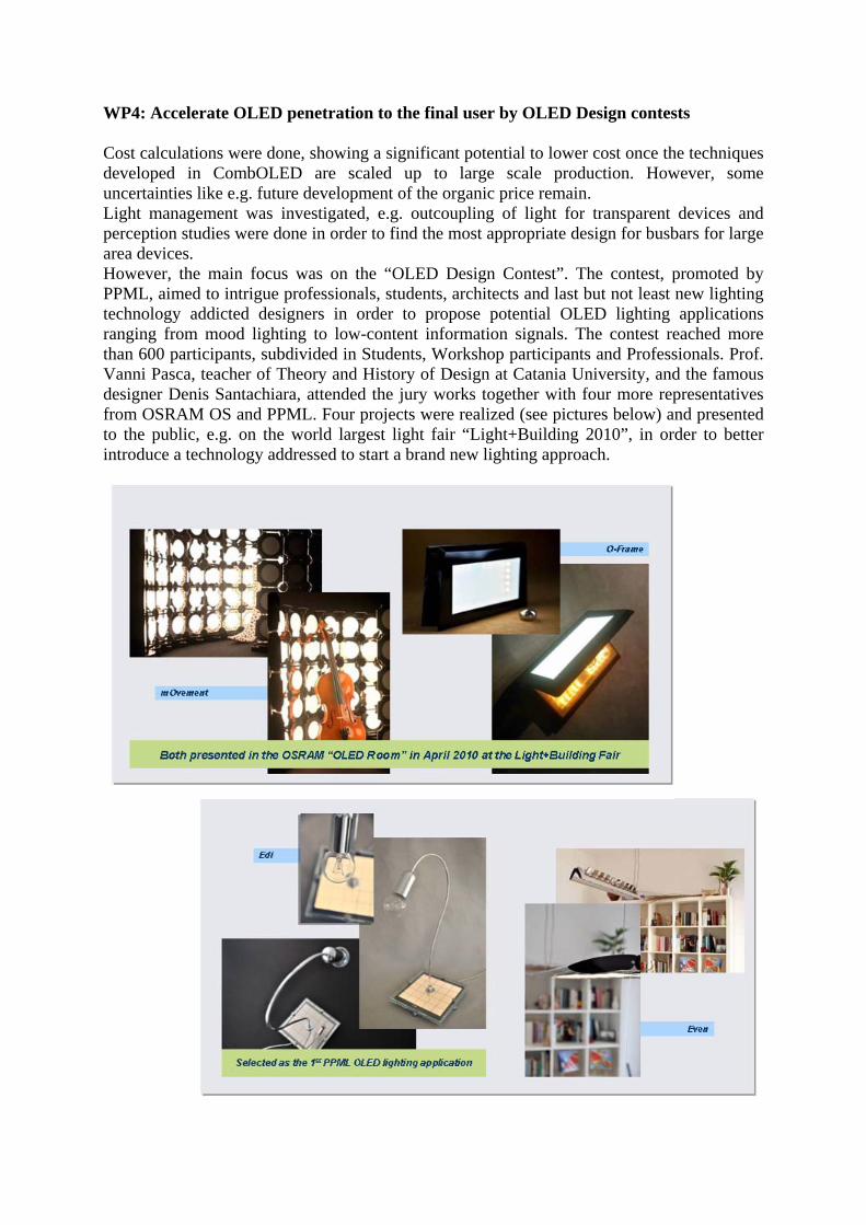
WP4: Accelerate OLED penetration to the final user by OLED Design contests Cost calculations were done, showing a significant potential to lower cost once the techniques developed in CombOLED are scaled up to large scale production. However, some uncertainties like e.g. future development of the organic price remain. Light management was investigated, e.g. outcoupling of light for transparent devices and perception studies were done in order to find the most appropriate design for busbars for large area devices. However, the main focus was on the “OLED Design Contest”. The contest, promoted by PPML, aimed to intrigue professionals, students, architects and last but not least new lighting technology addicted designers in order to propose potential OLED lighting applications ranging from mood lighting to low-content information signals. The contest reached more than 600 participants, subdivided in Students, Workshop participants and Professionals. Prof. Vanni Pasca, teacher of Theory and History of Design at Catania University, and the famous designer Denis Santachiara, attended the jury works together with four more representatives from OSRAM OS and PPML. Four projects were realized (see pictures below) and presented to the public, e.g. on the world largest light fair “Light+Building 2010”, in order to better introduce a technology addressed to start a brand new lighting approach.

1.4 The potential impact and the main dissemination activities and exploitation of results
The consortium is convinced that CombOLED has a very high strategic impact for Europe. Competitiveness in Lighting Industry: OLED lighting is truely facing a highly competitive field. Very recent announcements in the beginning of 2011 say that Panasonic Electric Works and Idemitsu Kosan established a joint venture for lighting production, Konika Minolta is offering OLED lighting products as well as many announcements to make the technology available in 2011 from e.g. NEC, Kaneka, Panasonic Electric Works, Pioneer (all Japan), LG Chem (Korea) and finally Mosaer Baer (US). Unlike displays where major innovations were done in Europe and then taken over by Asian and US economy the lighting industry is currently dominated by European companies. They are employing more than 35.000 people in various manufacturing locations all over the European continent to produce light sources for nearly all lighting applications, not counting numerous additional jobs in the OEM and supply chain. However, many of these businesses are using mature and well established technologies based on temperature radiators, gas discharge and UV excited phosphors. Since a few years they are facing a new, disruptive technology called Solid State Lighting. Inorganic LEDs and OLEDs fall under this category. These technologies require production know how which is based more on semiconductor manufacturing than on classical glass treatment technologies. As a result new competitors with according background appeared and do now have the opportunity to enter the lighting market. Inorganic LEDs – which just recently passed the threshold of available lumen packages, high efficiency and low costs to move into general lighting – are already dominated by Asian companies like Nichia, Toyoda-Gosei, Stanley, Everlite and others and US based companies like Cree. Within Europe, only OSRAM Opto Semiconductors operates a new, modern factory for inorganic LED production in Germany. It is essential for European companies to keep the leadership in new lighting technologies with new features like flatness and transparency which offer the opportunity to address also many new applications, thus offering growth potential. This was addressed by the CombOLED project which significantly contributed to establishing OLED development and production in Europe by building knowledge and providing skilled personnel to this industry. It is clear that, without focused multidisciplinary initiatives – supported by the commission – the chances of establishing high-tech production facilities within Europe will become more and more difficult in the future. In view of several overseas programs like the Solid State lighting program of the US Department of Energy (63 mn US$ per year until 2020, half of the money for OLED), the Japanese NEDO initiative (4.3 bn JPY from 2004 to 2011) and the new Korean Initiative by MOCIE (20,7 mn US$ over 7 years until 2013) the urgent need for similar European programs gets very clear. The above mentioned initiatives include the participation of well-known companies like General Electric, Matsushita Electric Works, NEC Lighting and LG Electronics. This clarifies that new competition can be expected from fields like OLED display manufacturing. This brief comparison shows that the competition in the pre-phase of market entry is fierce and there is a threat that a technological field, forming the basis for a huge market, is withdrawn from Europe. The need of supporting OLED programs – started by the OLLA project – has therefore significantly increased.

The CombOLED consortium includes – amongst others – industrial partners who contribute know-how in very important parts of the supply chain, i.e. base materials such as substrates, deposition equipment such as printers, and OLED manufacturers. The product aspect is covered by PPML, a highly innovative SME which will put strong emphasis on the exploitation of OLED features to realise new products in the future. A pioneering role with regard to other European luminaire and lighting sign manufacturers is foreseen. The development of driving electronics and interconnection schemes has the potential to contribute to standards, consequently keeping Europe in a leading role in lighting industry.

Dissemination: The main mechanisms used for the dissemination of knowledge generated in the project outside the consortium are: a project website (www.comboled-project.eu), the publishing of papers in high level scientific journals, press releases, active participation and presentations at professional conferences and trade shows. A very special case for CombOLED was the execution of an OLED design contest which requires a promotion campaign. This campaign includes special training sessions and OLED info events at design schools to make clear OLED opportunities to product designers. The academic and research institute partners will be in particular involved in dissemination activities. Overall more than 50 dissemination actions took place. Below some impressions from some of the events are shown:


Exploitation of results The CombOLED consortium is a balanced research effort between industrial partners, public research institutes and higher education institutes. All partners have plans and possibilities for the exploitation of the knowledge gained during and after the CombOLED project. The industrial consortium almost perfectly reflects a supply chain. Therefore the exploitation plans of the different partners do not interfere with each other but moreover do complement one another. It is expected, that within at latest 3 years after the CombOLED project the developments done in CombOLED will we implemented in early products and engineering samples, for example transparent OLED with thin film encapsulation on low cost substrates. At least one of the demonstrators developed in CombOLED (EDI) will be commercially available as well, soon additional additional products based on the OLED Design Contest are expected to follow.

1.5 Consortium / Website CombOLED started on January 1st 2008 with the partners Osram Opto Semiconductors (coordinator), Siemens, CEA-LETI, University of Valencia, Saint Gobain Recherche, PPML Lighting Solutions and Schreiner Group as an ICT funded project under the contract number 215934. More information can be found at the website: www.comboled-project.eu.
The CombOLED consortium
The CombOLED team