project final report - european commission : … · project final report ... ; logo of the 7th fp:...
TRANSCRIPT
PROJECT FINAL REPORT
Deliverable D0.4:”Public report of project’s results”
Grant Agreement number: 223882
Project acronym: MEMSPACK
Project title: Zero- and First-level Packaging of RF-MEMS
Funding Scheme: FP7– Small or Medium-scale focused research project
Period covered: from 1-6-2008 to 29-2-2012
Name, title and organisation of the scientific representative of the project's coordinator1:
Dr. Harrie A. C. Tilmans, IMEC (Leuven, Belgium)
Tel: +32 16 288 173
Fax: +32 16 281 576
E-mail: [email protected]
Project website2 address: www.memspack.eu
1 Usually the contact person of the coordinator as specified in Art. 8.1. of the grant agreement
2 The home page of the website should contain the generic European flag and the FP7 logo which are available in
electronic format at the Europa website (logo of the European flag: http://europa.eu/abc/symbols/emblem/index_en.htm
; logo of the 7th FP: http://ec.europa.eu/research/fp7/index_en.cfm?pg=logos). The area of activity of the project should
also be mentioned.

4.1 Final publishable summary report
Executive Summary:
A critical success factor hampering the commercialization of RF-MEMS has been the development, or, for
that matter, the availability, of an appropriate packaging technology. Until the MEMSPACK project was
launched, there had not been sufficient focused effort towards solving this issue. The FP7 supported
MEMSPACK project has tackled the packaging issue. The project has started June 1, 2008 and has ended
February 29, 2012.
The project’s main objective is to develop and to characterize generic 0-level (or wafer-level) and 1-level
packaging solutions for housing a large variety of RF-MEMS components and systems. This has been done
through 2 or 3 development cycles, each cycle encompassing design, modeling, simulation, process
technology development and full batch fabrication, and test and characterization. As many as 6 packaging
technologies have been developed, of which three are based on 0-level “chip capping” (involving W2W or
D2W bonding relying on BCB or solder bonds), two on 0-level “thin film capping” processing (relying on
BCB thin film or on porous aluminum oxide thin films), and one on 1-level packaging technology (which is
based on LTCC). These 6 technologies implement different topologies for the high frequency (RF)
feedthroughs. Much of the development effort is dedicated to making the right trade-off between the RF
characteristics, the hermeticity and the thermo-mechanical characteristics of the packages and of the electrical
feedthroughs. Moreover, as an integral part of the project, test methodologies and dedicated test structures for
characterizing the RF, thermo-mechanical and hermeticity characteristics of the packages, are developed.
The different packaging technologies have been evaluated on the basis of a set of baseline specifications
defined with the help and input from the IAB. While some of the technologies under development score best
on RF characteristics (good characteristics up to 70 GHz, and e.g., insertion loss down to 0.1 dB and return
loss up to 30 dB) and on low processing temperature (down to 250 °C), others show better hermeticity (with
helium leak rates currently down to 10-15
mbar•l/s), and/or better robustness against thermo-mechanical loads
such as high ambient temperatures and high back-end pressure (e.g., 30 or even 90bar as exerted during epoxy
overmolding). All 0-level packaging technologies have been demonstrated with CPWs as RF signal lines,
whereas the 1-level technology based on LTCC processing has been demonstrated with CPWs as well as
microstrip lines.
A specific outcome of the project is the “RF-MEMS packaging design guidelines”, which can be used by
industry for the development and exploitation of RF-MEMS. These guidelines describe in a comprehensive
manner the project outcome, thereby not only discussing the design of the package, but also the choice of
materials and processes implemented for a wide span of (complementary) packaging technologies together
with test procedures and characterization methods for the package. All of the MEMSPACK wafer level
packaging technologies are capable of providing low profile packages, compatibility with front end MEMS
and CMOS processing and compatibility with higher level packaging technologies. Not surprisingly perhaps,
it was concluded that the “Holy Grail package” does not exist (at least was not among the 6 packaging concept
as investigated by the consortium). Each one of the 6 packaging concepts has its own specific pro’s and con’s
and the choice of the package can only be made in view of the application. Thanks to the generic nature of the
6 MEMSPACK packaging concepts, they cover a wide range of potential applications, in particular in
consumer products (including hand held devices), automotive and space and aviation.
The technologies and the design, modeling and test competences as developed within the MEMSPACK are
prepared for commercial exploitation and industrial application, in some cases through recent spin-outs from
the below mentioned mother organizations. Several packaging technologies have reached a maturity level
which allows direct transfer of the technology to any industrial party interested.
The consortium partners in the project have been selected so that the whole development chain from
design&modeling via fabrication and test&characterization (including reliability testing) to benchmarking and
demonstrator fabrication is fulfilled. The project partners are: Imec (Belgium), VTT (Finland), FhG-ISiT
(Germany), University of Perugia (Italy), FBK (Italy), CNRS-IEMN (France) and MEMS Technical
Consultancy (The Netherlands). Further, an Industrial Advisory Board (IAB), consisting of 9 members, has
been installed at the beginning of the project. Apart from giving general guidance and providing input (on e.g.
the baseline specifications), the IAB plays an important role in guiding the consortium partners on exploitation
and industrialization of the results and on the follow-up of development activities. Contact details can be
found on the project website: www.memspack.eu
MEMSPACK: Summary description of project context and objectives
General introduction: (RF-)MEMS packaging
(RF-)MEMS devices, unlike ICs, contain movable fragile parts that must be packaged in a clean and stable
environment. The package or encapsulation should not only offer protection to the MEMS during operation
but also during fabrication. The specific ambient of the package housing depends on the type of RF-MEMS.
RF-MEMS switches for instance are preferably housed in an inert ambient (e.g., a dry nitrogen) at
atmospheric (or “slightly” below atmospheric) pressure. The same applies to RF-MEMS varactors (variable or
tunable capacitors) and variometers (tunable inductors). RF-MEMS resonators on the other hand require a
high level of vacuum (e.g., ambient pressure < 1 Pa) in order to attain high frequency stability and to have
sufficiently low damping at resonance. Practically all MEMS are adversely affected by corrosive ambients
like moisture. All in all and to ensure stability of the (RF-)MEMS device, the package must offer hermetic (or
near-hermetic) seals. Sealing and encapsulation are crucial so as to provide the required reliability of the
packaged devices.
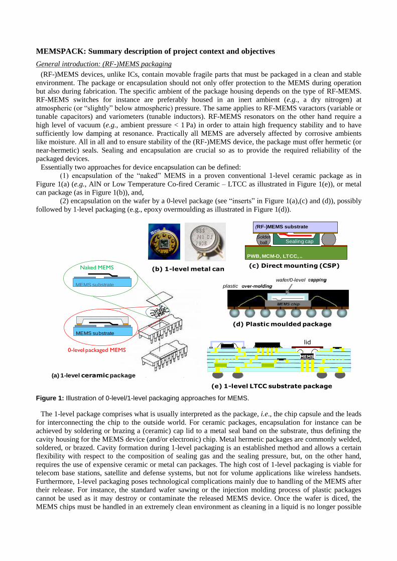
Essentially two approaches for device encapsulation can be defined:
(1) encapsulation of the “naked” MEMS in a proven conventional 1-level ceramic package as in
Figure 1(a) (e.g., AlN or Low Temperature Co-fired Ceramic – LTCC as illustrated in Figure 1(e)), or metal
can package (as in Figure 1(b)), and,
(2) encapsulation on the wafer by a 0-level package (see “inserts” in Figure 1(a),(c) and (d)), possibly
followed by 1-level packaging (e.g., epoxy overmoulding as illustrated in Figure 1(d)).
(b) 1-level metal can
(a) 1-level ceramicpackage
MEMS substrate
MEMS substrate
Naked MEMS
0-level packaged MEMS
plastic
wafer/0-level
PWB, MCM-D, LTCC, ..
(RF-)MEMS substrate
Solder
ball Sealing cap
(c) Direct mounting (CSP)
(d) Plastic moulded package
MEMS
(e) 1-level LTCC substrate package
lid
Figure 1: Illustration of 0-level/1-level packaging approaches for MEMS.
The 1-level package comprises what is usually interpreted as the package, i.e., the chip capsule and the leads
for interconnecting the chip to the outside world. For ceramic packages, encapsulation for instance can be
achieved by soldering or brazing a (ceramic) cap lid to a metal seal band on the substrate, thus defining the
cavity housing for the MEMS device (and/or electronic) chip. Metal hermetic packages are commonly welded,
soldered, or brazed. Cavity formation during 1-level packaging is an established method and allows a certain
flexibility with respect to the composition of sealing gas and the sealing pressure, but, on the other hand,
requires the use of expensive ceramic or metal can packages. The high cost of 1-level packaging is viable for
telecom base stations, satellite and defense systems, but not for volume applications like wireless handsets.
Furthermore, 1-level packaging poses technological complications mainly due to handling of the MEMS after
their release. For instance, the standard wafer sawing or the injection molding process of plastic packages
cannot be used as it may destroy or contaminate the released MEMS device. Once the wafer is diced, the
MEMS chips must be handled in an extremely clean environment as cleaning in a liquid is no longer possible
at this stage. All this makes that packaging is preferably carried out according to the 2nd
approach, i.e., on the
wafer during wafer processing, prior to die singulation. This packaging step is referred to as wafer-level or 0-
level packaging. Illustration of 0-level capped MEMS are presented in (the inserts) of Figure 1(a),(b) and (c).
There is clearly a trend observable towards 0-level packaging for MEMS.
The 0-level packaging creates an on-wafer device scale enclosure around (or sealed cavity for) the MEMS
device, serving as a first protective interface. Zero-level packaging in fact leverages the batch fabrication
features of front-end wafer processing. For the 0-level packaging, two general approaches have been taken,
here referred to as “thin-film capping” and “chip-capping”, both of which have been addressed in
MEMSPACK. In addition to a low-cost fabrication process and physical protection, the 0-level package must
be strong, equipped with low-loss electrical RF signal feedthroughs and be (near-)hermetic, preventing any
particles and moisture from migrating into the region of the MEMS and the region underneath the released
MEMS structure. On the other hand, 0-level packaging should not increase the die form factor too much, both
for cost reasons and for implementation reasons. Cell phones for instance put a constraint on the total height
of the packaged die. Once 0-level packaged, the wafer can be diced without any danger of demolishing the
MEMS device. The individual chip assemblies can next be mounted via wire-bond or flip-chip solder
bumping in a low-cost plastic molded 1-level package, e.g., SOIC-8 or BGA package, or, in a more costly 1-
level ceramic or metal package. The latter is done in case the 0-level package only serves as a basic protection
(e.g., during dicing) but is not sufficient in providing the required reliability and performance of the packaged
MEMS. Alternatively, the 0-level packaged device can be handled as a chip scale package (CSP) to be
directly joined to a printed wiring board. The 1-level package provides mechanical and environmental
protection to the devices they hold, but not without degrading the electrical performance. At microwave
frequencies (and higher) the impact the package has on the electrical performance becomes an important
element in the design of the device. Plastic molded packaging is the most common low-cost 1-level packaging
solution applicable for frequencies below several GHz. Careful choice of the plastic molding material and the
RF design of the leadframe allows use up to 10GHz. For use at higher frequencies, ceramic 1-level packages
based on multi-layer LTCC (Low Temperature Co-fired Ceramic) or HTCC (High Temperature Co-fired
Ceramic) technology, employing low loss dielectrics combined with flip-chip assembly of the device for short
interconnects, exhibit the potential for good performance into the millimeter wave regime (as high as 80GHz).
Without any doubt, packaging is one of the most important issues towards industrialization and
commercialization. It is now recognized that the package is an integral part of the MEMS device: “A MEMS
without a package is not a MEMS”. One of the functions of the package is signal distribution, and therefore, it
is fairly obvious that the RF performance may very well be (adversely) affected due to interference of the
package. In an ideal package the RF characteristics of the RF-MEMS device before and after 0-level
packaging should be the same, but this is something that is not at all evident to achieve. In effect, low-loss RF
transitions are required, in addition to minimal induced loss and detuning of the transmission lines due to
proximity coupling to the package. Moreover, testing the RF performance during processing is important to
improve yield and lower the costs. For this reason the design and technology should be chosen in a way to
establish not only an acceptable off chip RF performance but at the same time an easily testable and properly
packaged device while maintaining good device performance. The successful development of an (RF-)MEMS
device or system requires an "integrated design concept". Therefore, the structural design, the design of the
electromechanical transducer, the microwave design, design for proper testability, the micromachining
fabrication technology and last but not least the package design and technology should be addressed at the
same time, early in the design stage. Thus, in order not to be in for a surprise in the end, the choice of the
package technology and the package design should be taken up in the design process right away from Day 1.
Project context:
Future personal and ground RF communications systems and communications satellites necessitate the use
of highly integrated RF front-ends, featuring small size, low weight, high performance and low cost. Off-chip,
bulky passive RF components, like discrete PIN diode switches and ceramic filters, are limiting further chip
scaling. MEMS technology is now rapidly emerging as an enabling technology to yield a new generation of
high-performance RF-MEMS passives, like switches (displaying superior RF characteristics, like low
insertion loss and good linearity), high-Q Si-based resonators (to replace the bulky quartz crystals) and tunable
filters. RF-MEMS has been demonstrated to be a key technology for future adaptive and reconfigurable RF-
communication systems. In various research initiatives, many of them supported by the European
Commission, the specific advantages of RF-MEMS components, like lower loss, superior linearity and higher
Q as well as lower power consumption have been shown. RF-MEMS devices allow to build up completely
new RF-system architectures with increased performance and functionalities like reconfigurable RF-front-
ends in handsets and base stations, or highly integrated phase-array antennas for agile communication links.
Despite these initiatives however, following critical success factors, hampering the commercialization of (RF-
)MEMS, can be identified:
(1) the accessibility of existing IC foundries
(2) the manufacturing cost
(3) the (long-term) reliability and,
(4) the development of an appropriate packaging technology.
The MEMSPACK project has tackled the latter: “The packaging of the RF-MEMS”. Although MEMS
packaging has been taken up in previous European funded projects, the attention for the research efforts in
many of these projects was centred on the development and the demonstration of “a higher order system”.
Packaging, although addressed, was very often overshadowed by the drive of achieving “the system
demonstrator”. This has resulted in many unsolved packaging issues, which are addressed within
MEMSPACK. MEMSPACK has explored and assessed RF-MEMS packaging on one hand with respect to the
RF and encapsulation performance, but on the other hand also with respect to commercial targets.
Manufacturability, testability, reliability, time-to-market and last not least, cost of MEMS packaging has been
evaluated in depth.
The partners in the project have been selected such that the whole development chain from
design&modeling via fabrication and test&characterization to benchmarking and demonstrator fabrication is
fulfilled. The project partners with their main roles are:
- IMEC (Belgium): coordinator, supplier of 0-level packaging technology
- VTT (Finland): supplier of 1-level packaging technology
- FhG-ISiT (Germany): supplier of 0-level packaging technology
- University of Perugia (Italy): RF design and characterization of the package
- FBK-irst (Italy): supplier of (RF-MEMS) test vehicles to characterize the package
- CNRS-IEMN (France): RF design and test, supplier of 0-level packaging technology
- MEMS TC (The Netherlands): thermomechanical design, primary interface to the IAB
The fact that industry is not directly present in MEMSPACK as a full beneficiary does not at all mean that
this project has aimed only on academic objectives. All beneficiaries have close bilateral industrial
relationships in the RF-MEMS field and are well aware on the industrial needs. The absence of industrial
partners (except for the SME MEMS TC) in the project, made that an Industrial Advisory Board (IAB) was
established right from the start during the first month of the project. The alternative of including an industrial
partner (playing the role of end-user, IDM, foundry service, etc.) would bring about “the risk” of developing a
package solely for that particular industrial partner (or partners), and thus would jeopardize the generic nature
of the project. And, this has never been the intention of the project. The main objective of the project (see also
below) is to develop generic (RF-)MEMS packaging technologies and to be independent, i.e., not linked
somehow to any industrial company. Moreover, by installing an IAB, a larger community of end-users and
foundries can be reached. The IAB has provided input (e.g., on specifications) and moreover guidance on
which direction to take and where to put the focus of the developments within the project. The IAB is
composed of 9 members: Baolab (Sp), DelfMEMS (Fr), EADS (D), EPCOS Netherlands (NL), NovaMEMS
(Fr), NXP Research (NL), Optoi (It), Thales-Alenia-Space (Fr) and Selmic (Fin).

Project objectives
The main objective of the MEMSPACK project is:
To (further) develop and to characterize generic 0-level & 1-level packaging technologies for housing
(RF-)MEMS components and systems.
The project has primarily dealt with the 0-level packaging of (RF-)MEMS, but an example of 1-level
packaging based on LTCC has been worked out in detail as well.
Specific objectives set forth at the start of the project are:
To characterize the RF behaviour of the 0- and 1-level package through simulations
To verify/validate the RF simulation against measurements
To assess the range of applicability (RF performance, size, cost, compatibility, higher level packaging,
assembly, interconnect, …) of the different RF feedthrough concepts/technologies
To assess the impact/consequence of the 0-level package on the 1-level package (and the 2-level
package) and vice versa
To assess the compatibility of the 0- and 1-level packaging with the front end processing and vice
versa.
To assess and improve the reliability of the various 0-level packaging technologies
To assess and compare the hermeticity of the 0- and 1-level package for the different packaging
approaches in view of the application
To assess and compare the thermomechanical and structural behaviour of the 0&1-level package for
the different packaging approaches.
To assess the impact of the 0- and 1-level packaging (technology, thermomechanical, electro-
magnetic, ...) on the behaviour of the RF-MEMS.
To assess the impact, the constraints and the potential of the RF-MEMS packaging on the system
integration.
To formulate 0- and 1-level RF MEMS packaging guidelines for RF(-MEMS) engineers.

Description of the main S&T results/foregrounds
The main objective of the MEMSPACK project is to (further) develop and to characterize generic 0-level (or
wafer-level) & 1-level packaging solutions for housing (RF-)MEMS components and systems. This has been
done through 2 or 3 development cycles carried out for each packaging concept, each cycle encompassing
design, modeling, simulation, process technology development and full batch fabrication, test and
characterization and the package evaluation (impact of the package on the device performance towards
meeting industrial specifications as defined by the IAB). As many as 6 packaging technologies or concepts (as
they are called within the MEMSPACK project), have been developed. A schematic overview of the 6
concepts, indicating some specific characteristic of each concept, is presented in Figure 2. Three concepts (#1,
#2 and #3) are based on 0-level “chip capping” (involving W2W or D2W bonding), two (#4 and #5) on 0-
level “thin film capping” processing, and one (#6) on 1-level packaging technology based on LTCC. In the
case of 0-level chip-capping, it is common practice to bond a (recessed) capping wafer (or die) onto the
MEMS device wafer. The bonding & sealing ring is typically 50 to 300 m in width, whereas the cap has a
die thickness that is typically in the range of 100 to 700 m. Chip-capping is done either as a chip-to-wafer
(C2W), also called die-to-wafer (D2W), or as wafer-to-wafer (W2W). The MEMSPACK chip capping
packaging concepts #1, #2 and #3, rely on a CuSn-based solder, BCB and AuSn solder bond and seal,
respectively. For thin-film capping, the cap is made of a thin film of metal, dielectric or semiconductor with
thicknesses in the range of 1 to 10 m. Thin film capping typically relies on a 2nd
level of surface-
micromachining, this way leveraging on the front-end processing of the MEMS. The MEMSPACK thin film
packaging concepts #4 and #5 rely on BCB thin film or on porous aluminum oxide thin films, respectively.
Besides the packaging concepts quite a large effort has been spent on the development on the right test
structures (e.g., humidity sensors or cantilever MEMS for pressure sensing) used to characterize the various
packages (these test structure are conveniently referred to as concept#0).
(b) Concept#2 (Chip cap; horizontal)
(c) Concept#3 (Chip cap; buried)
(e) Concept#5 (Thin film cap; planar)
(f) Concept#6 (1-level; LTCC; vertical&horizontal)
(d) Concept#4 (Thin film cap; buried)(a) Concept#1 (Chip cap; TSVs)
MEMS
Pyrex Glassplanar
feedthroughPyrex Glassplanar
feedthroughHRSi substrate
HRSi Chip Cap
Pyrex Glass
MEMS
HRSi substrate
BCB thin film CAP
Planar feedthrough
Overcoat nitride (optional)
35 μm18 μm
100 -200 μm
CA
PMEMS
Al-buried
feedthroughDielectric layer
Si CAP
Si
Au
LTCC lid
BGA balls
LTCCMEMS Wire bond
MEMS substrate
Buried feedthrough
Thin film Cap
MEMSMEMS
MEMS substrate
CAP (100um)TS
V
Figure 2: Schematic illustration of the six packaging concepts as developed in MEMSPACK.
Prior to completing the chip layout, extensive and detailed design, modelling and simulation (DMS) of each
of the six concepts has been carried out. The DMS was carried out along two main paths:
o Thermomechanical DMS, addressing the various mechanical specs, and dealing with: residual stress
and/or initial strain in the packaging materials, maximum stresses occurring in the package, in the die
and at interfaces, and, the impact on the RF-MEMS component and system characteristics due to
deformations in the die and the package.
o Electrical (electromagnetic and circuit) DMS, addressing the various electrical (RF) specs and dealing
with: design of (wideband) electrical RF feedthroughs (up to 220GHz); interaction between the package
and the RF circuit, e.g., detuning due to proximity coupling of the cap to the RF circuit.Of importance,
in particular for a package for RF-MEMS, these 6 packaging technologies implement different
topologies for the high frequency (RF) signal feedthroughs. In designing the RF feedthroughs, a large
portion of the development effort has been dedicated in making the right trade-off for achieving the
desired RF characteristics on the one hand and, the hermeticity and the thermo-mechanical
characteristics on the other hand.
In part in parallel with the DMS, the relevant critical parameters as identified in the process flows for each of
the concepts were verified. The first development cycle(s) was(were) done for empty packages. This way a
baseline process for all 6 packaging concepts has been set-up and empty package samples for all concepts
have been fabricated and became available for test. For 4 chosen concepts, the so-called proof-of-concepts
(based on concepts#3, #4, #5 and #6), a (third and) final development cycle was done with actual “MEMS
inside”.
Test and characterization results, e.g., on the RF characteristics, mechanical strength and hermeticity, have
been gathered for all 6 concepts. Extensive reliability testing (including “highly accelerated stress testing
(HAST)”, pressure cooker test (PCT) and epoxy overmolding) has been carried out. The different packaging
technologies were evaluated on the basis of a set of baseline specifications put together with the help of the
IAB. While some of the technologies under development score best on RF characteristics (good characteristics
up to 70 GHz, and e.g., insertion loss down to 0.1 dB and return loss up to 30 dB) and on low processing
temperature (down to 250 °C), others show better hermeticity (with helium leak rates as low as 10-15
mbar•l/s),
and/or better robustness against thermo-mechanical loads such as high ambient temperatures and high back-
end pressure (e.g., 30bar and 90bar as exerted during epoxy overmoulding). All 0-level technologies have so
far been demonstrated with CPWs as RF signal lines, whereas the 1-level technology based on LTCC
processing has been demonstrated with CPWs as well as microstrip lines.
It is beyond the scope of this public report, in part because of the confidential nature of some of the results,
to describe all the details of the development of the various packaging concepts. Without further comments, a
flavor of the results obtained, together with some package specifics for each concept, is presented in Figure 3,
Figure 4, Figure 5, Figure 6, Figure 7, Figure 8, and Figure 9, for respectively concept#0 (front (MEMS) test
structures), concept#1, concept#2, concept#3 (=PoC-1), concept#4 (=PoC-2a), concept#5 (=PoC-2b), and
concept#6 (=PoC-3).
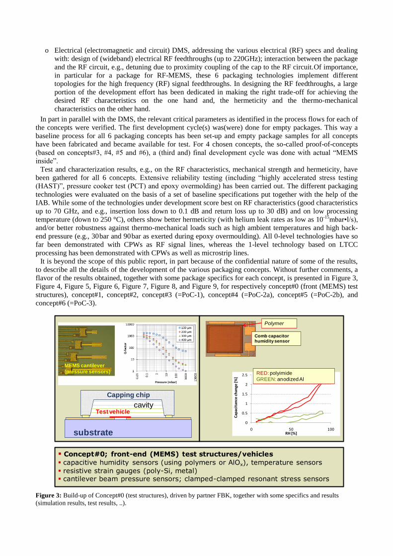
Concept#0; front-end (MEMS) test structures/vehicles
capacitive humidity sensors (using polymers or AlOx), temperature sensors
resistive strain gauges (poly-Si, metal) cantilever beam pressure sensors; clamped-clamped resonant stress sensors
substrate
Capping chip
cavityTest vehicle
Polymer
Comb capacitor humidity sensor
0
0.5
1
1.5
2
2.5
0 50 100
Cap
acit
ance
ch
ange
[%]
RH [%]
FBK_S25A_24_#3_Vac=100mV (poly)
FBK_S25B_23_#1_Vac=100mV (anod. Al)
RED: polyimide
GREEN: anodized Al
MEMS cantilever
(pressure sensors)
Figure 3: Build-up of Concept#0 (test structures), driven by partner FBK, together with some specifics and results
(simulation results, test results, ..).

HRSi substrate
Se
ali
ng
ri
ng
MEMS
CAP (HRSi)TS
V
Solder
(Sn, ..)
Cu
100 m
Ve
rtic
al
Inte
rco
nn
ec
t
Se
ali
ng
ri
ng
Ve
rtic
al
Inte
rco
nn
ec
t
Cu
CuCuxSny
Cu
-2.5
-2
-1.5
-1
-0.5
0
0 20 40 60
S 21
[dB]
F [GHz]
Port 1
Port 2
cap
substrate
Concept#1; 0-level “chip capping”; low real estate; flexible and versatile
metal solder (Cu/Sn/Cu) bond & seal (low-T 250 ⁰C) hermetic 100m thick HRSi cap with Cu TSVs for vertical RF feedthroughs
relatively complex technology (thinned wafers, TSVs, interconnect)
“#0 in #1”
Figure 4: Build-up of packaging Concept#1, driven by partner IMEC, together with some specifics and results
(simulation results, test results, ..).
Concept#2; 0-level chip capping; 250m thick HRSi cap; flexible&versatile
polymer (BCB) low-T (250⁰C) bond & seal not hermetic horizontal planar RF feedthroughs superior RF characteristics
relatively simple technology (and low cost)
HRSi
CPW HRSi
|S11
| (d
B)
10dB/div
5 10 15 20 25 30 35 40 450 50
-30
-20
-10
-40
0
freq, GHz
dB(S
(1,1
))dB
(S(3
,3))
|S21
| (dB
)
0.2 dB/div
5 10 15 20 25 30 35 40 450 50
-1.8
-1.6
-1.4
-1.2
-1.0
-0.8
-0.6
-0.4
-0.2
-2.0
0.0
freq, GHz
dB(S
(2,1
))dB
(S(3
,4))
S12-parameter vs. Temp. (traversing CPW)
Blue @ 100 °CRed @ 20 °C
S12 [dB]
0.2dB
Freq. [GHz]
MEMS
Pyrex Glassplanar
feedthrough
Bond pad
Pyrex GlassPlanar
RF feedthrough
HRSi substrate
HRSi cap 250 μm
50μm
100 μm-200 µm
BCB bond
(10-15m)
0.2 dB/div
Uzµm
Uz,max=-0.0024µm@20°C
Deformation(sim) 0
10
20
30
40
50
60
70
80
5x5
-3
5x5
-4
5x5
-5
5x5
-6
2x2
-3
2x2
-4
2x2
-2n
d-1
2x2
-2n
d-2
2x2
-2n
d-3
2x2
-2n
d-4
2x2
-2n
d-5
Concept #2
Sh
ea
r s
tre
ng
th (
MP
a) Shear strength
Figure 5:Build-up of packaging Concept#2, driven by partner IEMN, together with some specifics and results
(simulation results, test results, ..).

Concept#3/PoC-1; 0-level chip capping (W2W); 200-500m thick Si cap
metal solder (AuSn) bond & seal (280⁰C) hermetic horizontal buried feedthroughs good RF performance
mature technology; robust and reliable
0
20
40
60
80
100
120
Before treatment after PCT: 121°C
2bar, [up to 96h]
after Temperature
shock [1000 cyc.]
Sap
mp
les p
assed
GL
T [
%]
concept #3
concept #3bis
Thermal cycling and
pressure cooker test
CAP
MEMS
Al-buried
feedthroughDielectric layer
Si CAP
Si
Bo
nd
pa
d (A
u)
AuSn
bond
Diced wafer stack
PoC-1
Figure 6: Build-up of packaging Concept#3 (=PoC-1), driven by partner ISiT, together with some specifics and results
(simulation results, test results, ..).
Concept#4/PoC-2a; 0-level thin-film capping; dielectric (AlOx); 2-10m cap
dielectric (SiNy) or metal seal “hermetic”; very low profile; horizontal buried RF feedthroughs good RF performance
reliable; high hydrostatic strength epoxy molding up to 90bar
MEMS substrate
Buried (Al) feedthrough
Thin film Cap
MEMS
AlOx
Clean cavity
100µm Intentionally defined hole
Sealed for
‘hermeticity’
monitoring
Porous AlOxSiNy
AirHe
Ni-MEMS
Figure 7: Build-up of packaging Concept#4 (=PoC-2a), driven by partner IMEC, together with some specifics and
results (simulation results, test results, ..).

Concept#5/PoC-2b; 0-level “thin-film capping”; low profile;
polymer (5-20 m BCB) cap ( not hermetic) + overcoat nitride ( “hermetic”) horizontal planar RF feedthroughs very good RF performance
two-chip approach (unique process); flexible and versatile
Pyrex Glass
MEMS
HRSi substrate
BCB thin film CAP
Planar feedthrough
OvercoatNitride
(optional)35 μm
18 μm
100 -200 μmM
EM
S
sw
itc
hMSL
0 10 20 30 40 50 60
-60
-50
-40
-30
-20
-10
0
-20
-16
-12
-8
-4
0
Inse
rtio
n lo
ss (
dB
)
Re
turn
lo
ss, Is
ola
tio
n (
dB
)
Frequency (GHz)
Before packaging
After packaging
Isolation
Return loss
RF-MEMS switch
Isolation
RL
Figure 8: Build-up of packaging Concept#5 (=PoC-2b), driven by partner IEMN, together with some specifics and
results (simulation results, test results, ..).
Concept#6/PoC-3; 1-level packaging using LTCC techno; LTCC cap (lid)
ceramic and metal seal hermetic
horizontal&vertical RF feedthroughs; sub-optimal interconnects (wires, ribbon) mature technology (and low cost);flexible and versatile
LTCC lid
BGA balls
LTCCMEMS Wire bond
FC assembled chip in LTCC
“#5 in #6”“#0 in #6”
“#5 in #6”
ribbon
wire
on-chip
Figure 9: Build-up of packaging Concept#6 (=PoC-3), driven by partner VTT, together with some specifics and results
(simulation results, test results, ..).

One further important outcome of the project are the “RF-MEMS packaging design guidelines”, which can
be used by industry for the development and exploitation of RF-MEMS. The evaluation results of the package
technology demonstrators (together with examples from the literature) have been used to produce the RF-
MEMS packaging design guidelines. These guidelines describe in a comprehensive manner the outcome of
the project, thereby discussing not only the design of the package, but also the choice of materials and
processes implemented for a wide span of (complementary) packaging technologies together with test
procedures and characterization methods for the RF-MEMS package. Design guideline examples targeting a
robust structural thermo-mechanical design and a high performance RF design are available. All of the
MEMSPACK wafer level packaging technologies are capable of providing low profile packages,
compatibility with front end MEMS and CMOS processing and compatibility with higher level packaging
technologies. Not surprisingly perhaps, it can be concluded that the “Holy Grail package” does not exist (at
least was not among the 6 packaging concept as investigated by the consortium). Each one of the 6 packaging
concepts has its own specific pro’s and con’s and the choice of the package can only be made in view of the
application. Below Table 1 presents a benchmarking among the different packaging concepts on a number of
characteristics. Per characteristic, the best in class (indicated by a green circle) and the worst in class
(indicated by a red circle) for the 0-level packaging concepts are indicated (because of its very different
nature, the package concept#6, the 1-level LTCC package, did not take part in “the competition”). Thanks to
the generic nature of the 6 MEMSPACK packaging concepts, they cover a wide range of potential
applications, in particular in consumer products (including hand held devices), automotive and space and
aviation. Several packaging technologies have reached a maturity level which allows direct transfer of the
technology to any industrial party interested. The Table 1 can be used as an aid by users when selecting the
right packaging concept for a certain application.
Characteristic #1 #2 #3 #4 #5 #6
0-level Chip capping 0-level Thin film capping 1-level
“Specialty”Metal seal,
TSVBCB bond Metal seal
Porous film
initial cap
Transferred
BCB capLTCC
RF behaviour +/- ++ + + ++ +
Hermeticity + - ++ + - (+) +
Choice of cavity ambient + - ++ - - +/-
Hydrostatic Strength +/- ++ ++ +/- - ++
Front-end compatibility + + +/- +/- + +/-
Back-end compatibility +/- + ++ +/- - ++
Reliability +/- - ++ + +/- +
Size increase (OH MEMS) ++ - - - + +/- +/-
Height/Form factor +/- +/- - ++ + +/-
Complexity/Cost - ++ +/- +/- + +
Manufacturability - - ++ + +/- + +
Maturity - + ++ +/- +/- ++
IP situation/uniqueness + +/- +/- + +/- +/-
MEMS substrate
CAP (100um)
LTCC lid
LTCCMEMS
Si CAP
MEMS substrate
Table 1: “Benchmarking” of the different packaging concepts as developed in MEMSPACK. Per characteristic, the best
in class (indicated by a green circle) and the worst in class (indicated by a red circle) for the 0-level package concepts are
indicated.
Impact, dissemination and exploitation
Impact
Wireless communication is showing an explosive growth of emerging consumer and military applications of
radio frequency (RF), microwave, and millimeter-wave circuits and systems. Future personal (hand-held) and
ground communications systems as well as automotive radar systems and communications satellites
necessitate the use of highly integrated agile RF front-ends, featuring small size, low weight, high
performance and low cost. Continuing chip scaling has contributed to the extent that off-chip, bulky passive
RF components, like high-Q inductors, ceramic and SAW filters, varactor diodes and discrete PIN diode
switches, have become limiting. Micro-machining or MEMS technology is now rapidly emerging as an
enabling technology to yield a new generation of high-performance RF-MEMS passives to not only replace
these off-chip (discrete) passives but moreover to allow for more integrated solutions in wireless
communication (sub)systems. RF-MEMS technology offers the potential to build a multitude of miniaturized
components as switches, voltage-tunable capacitors, high-Q inductors, film bulk acoustic resonators (FBAR),
dielectric resonators, transmission line resonators and filters, and mechanical resonators and filters. These
components offer specific advantages, like lower loss, higher isolation, superior linearity, higher Q, lower
power consumption and improved tunability as well as improved “integratability”. In various research
initiatives, many of them supported by the European Commission, the specific advantages of RF-MEMS
components have already been demonstrated. The use of MEMS technology is now opening new perspectives
for various wireless applications to achieve solutions with improved performance, compactness and also cost.
RF-MEMS may revolutionize the choices made in the architecture of transceiver systems and/or radar
antennas, by allowing completely new RF-system architectures with increased performance and functionalities
like adaptive and reconfigurable RF-front-ends in handsets and wireless LAN (like 60GHz radio), eventually
leading to cognitive radio as the next generation standard (targeting the optimal use of the frequency spectrum
by implementing opportunistic sharing of bandwidth). Furthermore, RF-MEMS will find use in base stations,
wireless sensor networks, and/or in highly integrated phase-array antennas for agile communication links. For
all these applications, it is fair to state that the major advantage of RF-MEMS is not so much in a replacement
at the component level, but rather as an enabling technology at the system level. This means that smart system
integration of RF-MEMS is the key for the success in industrialization. The MEMS components need to be
integrated with other passive and active components to build up RF-modules or sub-modules with advanced
functionalities. Needless to say, the challenge for most of the applications is high-density integration to further
reduce the size and the cost. Advanced smart systems integration technologies will be the key element to
secure competitiveness of European industry. Packaging is an integral part of these smart systems and can
contribute significantly to the overall size and cost of the product, spanning from 25% up to 75%, both in cost
as well in size. Furthermore the impact the package has on the device (or system) performance should not be
taken too lightly. Strong R&D efforts in the packaging of RF-MEMS as MEMSPACK has undertaken are
therefore clearly needed and justified in order to successfully build the smart RF systems of the future,
displaying superior performance and new functionalities, and this for a reduced size and cost.
Although MEMSPACK is focused on RF applications, the project results are of significant value also for
MEMS in general. The packaging issue is a major barrier to be overcome for the industrialization of MEMS,
in general. The 0-level and 1-level packaging technologies as well as the encapsulation and reliability test
methodologies are not restricted to RF-MEMS, but can easily be transferred to other MEMS, like
accelerometers, micromirror devices, gyroscopes, magnetometer (electronic compass), microbolometer and
many more. The MEMS however are limited to those that do not need to be in (direct) contact with the
ambient for their operation. As such many type of MEMS sensors, like pressure sensors and flow sensors, and
MEMS actuators, like microgrippers and micromotors, are excluded. Concluding, the impact of MEMSPACK
is enlarged substantially by not only addressing RF applications, but by addressing also other key application
areas, as MEMS for consumer or automotive.

Dissemination
With the consortium mainly consisting of national laboratories and two universities, dissemination has been
a key aspect of the project. The main mechanisms that has been used for the dissemination of knowledge
generated in the project among the scientific community was through submission and presentation of papers at
scientific and trade conferences, workshops and journals, including, but not limited to, the EC’s annual RF
MST Cluster Meetings. The progress of the project can also be followed in the publicly accessible part of the
MEMSPACK website, that has been updated regularly for rapid dissemination and which has been made
accessible to the community at large. Moreover, the results have been disseminated through the EC networks
of excellence PATENT-DfMM, AMICOM and RF PLATFORM, by the MEMSPACK beneficiaries that are
also participating in those NoEs. The MEMSPACK consortium has interacted with other FP7 projects,
including MEMS4MMIC, Regpot METU-MEMS, MOSART, WiserBAN, ARASCOM, AMICON TG
EuMA, and COWIN. All beneficiaries have been in particular involved in dissemination activities by means
of their industrial partnerships, leading role in state-of-the art R&D, and long-standing experience in EU
funded projects. Progress has been presented to the Industrial Advisory Board in the 3 scheduled IAB
meetings of which the last meeting was actually a one-day workshop. Moreover, results of the projects have
been gathered in concise overviews, suitable for RF designers, and have been conveyed through publications
and, outside the frame of the project, through education of students.
Exploitation
The national laboratories participating in the MEMSPACK consortium are all world-class R&D and training
centres, which perform R&D ahead of industrial needs by 3 to 10 years in microelectronics, nanotechnology,
design methods and technologies for ICT systems. Through their participation in the MEMSPACK project,
they have strengthened their positions as Europe’s leading Centres of Excellence for RF technology and
design methods. 3 of the partners have founded spinouts shortly before MEMSPACK started (UPG spun out
RF Microtech srl), or during the project in 2010 (FhG-ISiT and VTT spun out MEMS Foundry Itzehoe GmbH
and VTT Memsfab Ltd., reps.). These spinouts offer, among others, results from MEPACK on a commercial
basis. Collaborations between partners and IAB members that existed prior to MEMSPACK have been
strengthened by MEMSPACK (UPG and FBK with Optoi,, VTT with Selmic, IEMN with DelfMEMS, IMEC
with NXP and EPCOS). MEMS TC has provided services to several of the IAB members on a commercial
basis, in some cases this concerned competence built up in MEMSPACK. Europractice has expressed interest
in MEMSPACK technologies from partners or their spinouts that show commitment to maintain their
technology and to continue to offer their technology. These cases are currently being explored. All in all, there
has been a drive towards exploitation of the results in terms of:
Services in the field of package fabrication, package design and package test (and infrastructure)
Prototyping or low volume production at IMEC, VTT, ISiT and FBK, e.g., for IAB members but
also to any other interesting industrial partner and existing spin-out/start-up.
Technology transfer to industrial technology providers (foundries, package vendors) and
component/system manufacturers. Making available the developed package technology platforms
for industrialization in production fabs wherever an appropriate business case exists.
Patenting and licensing of results to industry. The protection of Intellectual Property will be sought
through patent applications. This is aimed at not so much for the beneficiaries to gain financial
benefit, but rather to protect the interest of European industry seeking to make use of these
innovations.
Spinouts from the project itself
More in particular the exploitation by the different beneficiaries is presented in Table B2 in section B of this
report.

Contact details
The 7 partners in the project are: (1) imec (BE), (2) VTT (FIN), (3) FhG-ISiT (DE), (4) UPG (IT), (5) FBK
(IT), (6) CNRS-IEMN (FR) and (7) MEMS TC (NL).
The coordinator of the project is imec (BE), contact details:
Dr. Harrie A. C. Tilmans Imec v.z.w., Kapeldreef 75 B-3001 Leuven Belgium E-mail: [email protected]
The primary contact for the consortium to the IAB is provided by MEMS TC (NL), contact details:
Dr. Siebe Bouwstra E-mail: [email protected]).
Contact persons for partner imec (BE) are: Dr. H. A. C. Tilmans (E-mail: [email protected]),
Dr. N. Pham (E-mail: [email protected]), and,
Dr. V. Cherman (E-mail: [email protected])
Contact persons for partner VTT (FI) are: Dr. T. Vähä-Heikkilä (E-mail: [email protected]), and,
Dr. M. Lahti (E-mail: [email protected])
Contact persons for partner FhG-ISiT (DE) are: Dr. B. Wagner (E-mail: [email protected]), and,
Dr. C. Huth (E-mail: [email protected])
Contact persons for partner UPG (IT) are: Prof. R. Sorrentino (E-mail: [email protected]), and,
Dr. P. Farinelli (E-mail: [email protected])
Contact persons for partner FBK (IT) are: Dr. B. Margesin (E-mail: [email protected]), and,
Dr. A. Faes (E-mail: [email protected])
Contact persons for partner CNRS-IEMN (FR) are; Prof. P.-A. Rolland (E-mail: [email protected]),
Prof. N. Rolland (E-mail: [email protected]), and,
Dr. S. Seok (E-mail: [email protected])
Contact person for partner MEMS TC (NL) is: Dr. S. Bouwstra (E-mail: [email protected])
The MEMSPACK website can be found at: http://www.memspack.eu.
Contract no.: 223882 The work described in this report was done under EC contract. Responsibility for the contract resides with the
author(s) or organization(s) preparing it.
EC Theme ICT

4.2 Use and dissemination of foreground
Section A (public)
Below Table A1 shows all scientific publications (journals and conference publications) from the beginning until after the end of the project.
Publications submitted and that are pending acceptance are also included.
TABLE A1: MEMSPACK LIST OF SCIENTIFIC PUBLICATIONS (STARTING WITH THE MOST IMPORTANT ONES, i.e., PEER REVIEWED JOURNAL PAPERS)
NO. Title Main author Title of the
periodical or the series
Number, date or
frequency Publisher
Place of publication
Year of publication
Relevant pages
Permanent identifiers
(if available)
Is/Will open access
provided to this
publication?
1
Polymer-based zero-level packaging technology for high frequency RF applications by wafer bonding/debonding technique using an anti-adhesion layer
Janggil Kim (IEMN)
Int. J. Precision Eng. And Manufacturing
Vol. 13(10), Oct. 2012
Springer Seoul (Korea) 2012 N/A N/A No
2
Modeling of gold microbeams as strain and pressure sensors for characterizing MEMS packages
Alessandro Faes (FBK)
Microsystem Technologies
March 4, 2012 Springer (Berlin / Heidelberg)
2012 1-7 http://dx.doi.org/10.1007/s00542-012-1457-5
No
3
Built-in self-limitation of masked aluminum anodization using photoresist
Joseph Zekry (IMEC)
Procedia Engineering
Vol. 25, 2011
Elsevier 2011 1633-1636
http://www.sciencedirect.com/science/journal/18777058/25
No
4
A Study on Millimetre-Wave Tunable Bandpass Filter Based on Polymer Cap Deflection
Seonho Seok IEMN)
Micromachines Vol. 3, Jan. 6, 2012
MDPI Publishing
Basel, (Switzerland)
2012 28-35 10.3390/mi3010028 Yes
5
Wafer-level thin film vacuum packages for MEMS using nanoporous anodic alumina membranes
Joseph Zekry (IMEC)
Transducers 2011
June, 2011 IEEE Beijing (China)
2011 974-977 10.1109/TRANSDUCERS.2011.5969507
No

TABLE A1: MEMSPACK LIST OF SCIENTIFIC PUBLICATIONS (STARTING WITH THE MOST IMPORTANT ONES, i.e., PEER REVIEWED JOURNAL PAPERS)
NO. Title Main author Title of the
periodical or the series
Number, date or
frequency Publisher
Place of publication
Year of publication
Relevant pages
Permanent identifiers
(if available)
Is/Will open access
provided to this
publication?
6
Modeling of gold microbeams for characterizing MEMS packages
Alessandro Faes (FBK)
Proc.of SPIE, Smart Sensors, Actuators, and MEMS V
Volume 8066, 2011
SPIE Prague (Czech republic)
2011 80660Z 1-9
http://dx.doi.org/10.1117/12.887571
No
7 Wafer-Level BCB Cap Packaging of Integrated MEMS Switches with MMIC
Seonho Seok (IEMN)
IEEE/MTT-S International Microwave Symposium
June 17, 2012 IEEE Montréal (Canada)
2012 N/A No
8
Polymer-based zero-level packaging technology for high frequency RF applications by wafer bonding/debonding technique using an anti-adhesion layer
Janggil Kim (IEMN)
MINAPAD 2012 April 24, 2012 iMAPS Grenoble (France)
2012 N/A No
9 Zero-level packaging for (RF-)MEMS implementing TSVs and metal bonding
Nga Pham (IMEC)
ECTC 2011 May 31, 2011 IEEE Florida, USA 2011 1588-1595
10.1109/ECTC.2011.5898723
No
10
Design of RF Feedthroughs in Zero-Level Packaging for RF MEMS Implementing TSVs
Hamza El Ghannudi (UPG)
MEMSWAVE 2011
June 28, 2011 Athens (Greece)
2011 N/A Yes
11 Metal-bonded, hermetic 0-level package for MEMS
Nga Pham (IMEC)
EPTC 2010 Dec. 8, 2010 IEEE Singapore 2010 1-6 10.1109/EPTC.2010.5702595
No
12 A capacitive humidity sensor using a positive photosensitive polymer
Nga Pham (IMEC)
21st MME workshop 2010
Sept. 26, 2010
Enschede (The Netherlands)
2010 60-63 N/A Yes
13
A novel wafer level bonding/ debonding technique using an anti-adhesion layer for polymer-based 0-level packaging of RF device
Janggil Kim (IEMN)
ECTC 2010 June 1, 2010 IEEE Las Vegas (USA)
2010 323-328 10.1109/ECTC.2010.5490954
No

TABLE A1: MEMSPACK LIST OF SCIENTIFIC PUBLICATIONS (STARTING WITH THE MOST IMPORTANT ONES, i.e., PEER REVIEWED JOURNAL PAPERS)
NO. Title Main author Title of the
periodical or the series
Number, date or
frequency Publisher
Place of publication
Year of publication
Relevant pages
Permanent identifiers
(if available)
Is/Will open access
provided to this
publication?
14
Design and manufacturing of wideband buried RF feedthroughs for wafer-level RF MEMS package
Hamza El Gannudi (UPG)
European Microwave Integrated Circuits (EuMIC)
Sept. 27, 2010
IEEE Paris (France) 2010 321-324 N/A No
15 On the LTCC Characterization in millimeter-waves
V. Kondratyev (VTT)
European Microwave Integrated Circuits (EuMIC)
Sept. 27, 2010
IEEE Paris (France) 2010 156-159 N/A No
16
EM Modelling, Design and Manufacturing of a 0-level package for RF-MEMS applications
Hamza El Gannudi
MEMSWAVE 2010
June 2010 Editura Academiei Romăne
Otranto (Italy), and, Bucureşti (Rom)
2010 (digest)
2011
- 97-104
N/A Yes
17
Thermo-mechanical design of a generic 0-level MEMS package using chip capping and Through Silicon Via’s
Bart Vandevelde (IMEC)
EuroSimE 2010 April 26, 2010 IEEE Bordeaux (France)
2010 7pages 10.1109/ESIME.2010.5464539
No
18
Thermo-mechanical simulations of RF-MEMS 0-level package based on wafer bonding by soldering
Siebe Bouwstra (MEMS TC)
EuroSimE 2010 April 26, 2010 IEEE Bordeaux (France)
2010 9 pages 10.1109/ESIME.2010.5464581
No
19
Thermo-mechanical design and modeling of porous alumina-based thin film packages for MEMS
Joseph Zekry (IMEC)
EuroSimE 2010 April 26, 2010 IEEE Bordeaux (France)
2010 7 pages 10.1109/ESIME.2010.5464584
No
20
Thermo-mechanical simulation of BCB membrane thin-film package
Seonho Seok (IEMN)
EuroSimE 2010 April 26, 2010 IEEE Bordeaux (France)
2010 4 pages 10.1109/ESIME.2010.5464577
No

TABLE A1: MEMSPACK LIST OF SCIENTIFIC PUBLICATIONS (STARTING WITH THE MOST IMPORTANT ONES, i.e., PEER REVIEWED JOURNAL PAPERS)
NO. Title Main author Title of the
periodical or the series
Number, date or
frequency Publisher
Place of publication
Year of publication
Relevant pages
Permanent identifiers
(if available)
Is/Will open access
provided to this
publication?
21
Thermo-mechanical simulations of LTCC packages for RF MEMS applications
Jaakko Lenkkeri (VTT)
EuroSimE 2010 April 26, 2010 IEEE Bordeaux (France)
2010 6 pages 10.1109/ESIME.2010.5464591
No
Submitted, pending acceptance:
22
Wafer-level thin film vacuum packages for MEMS using nanoporous alumina membranes, Part I. Design and fabrication
Joseph Zekry (IMEC)
Sensors & Actuators A: Physical
Submitted April 2012
Elsevier No
23
Wafer-level thin film vacuum packages for MEMS using nanoporous alumina membranes, Part II. Performance and reliability
Joseph Zekry (IMEC)
Sensors & Actuators A: Physical
Submitted April 2012
Elsevier No
24 Wideband LTCC modules with vertical transitions
Mikko Kaunisto (VTT)
IEEE Trans. On Microwave Theory and Techniques
IEEE No
25 Wideband LTCC modules with horizontal transitions
Mikko Kaunisto (VTT)
IEEE Trans. On Microwave Theory and Techniques
IEEE No
26 LTCC filter based on via resonators
V. Kondratyev (VTT)
42nd European Microwave Conference
IEEE Amsterdam (The Netherlands)
2012 No

Below Table A2 shows all dissemination activities from the beginning until after the end of the project.
TABLE A2: MEMSPACK LIST OF DISSEMINATION ACTIVITIES
NO. Type of activities Main
leader Title Date Place
Type of audience
Size of audience
Countries addressed
1 Scientific Publications “all” see Table A1 See table A1 See Table A1 Scientific community
Various (10-1000)
all
2 Other: Closed meeting MEMS TC 1st IAB meeting MEMSPACK 30 June 2008 Heraklion MEMSPACK IAB 8 France, Netherlands, Germany, Italy, Finland, Spain, Denmark
3 Other: Closed webinar MEMS TC 1st IAB webinar MEMSPACK 16 December 2009
Internet MEMSPACK IAB 7 France, Netherlands, Germany, Italy, Finland, Spain,
4 Other: Closed meeting MEMS TC 2nd IAB meeting MEMSPACK 28 June 2010 Otranto MEMSPACK IAB 4 France, Netherlands, Germany, Italy, Finland, Spain
5 Other: Closed webinar MEMS TC 2nd IAB webinar MEMSPACK 15 December 2009
Internet MEMSPACK IAB 9 France, Netherlands, Germany, Italy, Finland, Spain
6 Other: Closed meeting & workshop
MEMS TC 3rd IAB meeting + workshop MEMSPACK
26 January 2012
Amsterdam MEMSPACK IAB + EU officer
6 France, Netherlands, Germany, Italy, Finland, Spain
7 “Flyer” MEMS TC “RF MEMS Packaging” May 2011 COWIN website MST community 300 All
8 Poster VTT “RF MEMS Packaging”, Euripides Forum 2011
June 2011 Helsinki (Finland) MST community 300 All
9 Articles published in trade journals
MEMS TC MEMSPACK: 0- and 1-Level Packaging Tech-nologies for (RF-) MEMS
April 2011 Yole Micronews MST community 1,000 All
10 Articles published in trade journals
MEMS TC MEMSPACK: 0- and 1-Level Packaging Tech-nologies for (RF-) MEMS
April 2012 MEMS Technology Review
MST community 30,000 All
11 Presentations IMEC “MEMSPACK overview”, at RF MST Cluster meeting
June 2008 Heraklion (Greece) RF MST community in Europe
60 EU + Assoc. countries
12 Presentations IMEC “MEMSPACK overview”, at RF MST Cluster meeting
June 2009 Trento (Italy) RF MST community in Europe
60 EU + Assoc. countries
13 Presentations IMEC “MEMSPACK overview”, at RF MST Cluster meeting
June 2010 Otranto (Italy) RF MST community in Europe
60 EU + Assoc. countries

TABLE A2: MEMSPACK LIST OF DISSEMINATION ACTIVITIES
NO. Type of activities Main
leader Title Date Place
Type of audience
Size of audience
Countries addressed
14 Presentations IMEC “MEMSPACK overview”, at RF MST Cluster meeting
June 2011 Athens (Greece) RF MST community in Europe
60 EU + Assoc. countries
15 Presentations IMEC “MEMSPACK overview”, at RF MST Cluster meeting
July 2, 2012 Anatalya (Turkey) RF MST community in Europe
60 EU + Assoc. countries
16 Presentations MEMS TC “MEMSPACK”, at 1st Turkish National MEMS Conference
December 2010 Ankara (Turkey) Turkey MST community
100 Turkey
17 Workshop IMEC MEMSPACK”, at MINAmI Workshop (Parallel to ICT 2008)
November 26, 2008
Lyon (France) MINAmI project members
20 EU
18 Lectures VTT, IMEC, IEMN
“RF MEMS Packaging”, at 3 AMICOM summer schools
June 2009, 2010 and 2011
Toulouse (Fr), Padova (It), Toulouse (Fr)
Students, researchers
3x30 All
19 Lecture VTT, IMEC “RF MEMS Packaging”, at RF microsystem workshop EuMIC2011
2011 Manchester (UK) Conference participants
100 All
20 Lectures UPG, IEMN “RF MEMS design”, at university lecture courses
2009 onwards Students Italy, France
21 Networking with other EU projects
all
MEMS-4-MMIC, METU-MEMS, MINAmI, WiserBAN, ARASCOM, AMICOM TG EuMA, COWIN
2008 onwards Various places EU project consortiums
200 Europe
22 Project website MEMS TC www.memspack.eu 2008 onwards www Public + restricted pages for IAB and for EC
>1,500 hits world wide

Section B (confidential)
Part B1
Below Table B1 shows all applications for patents, trademarks, registered designs, etc. from the beginning until after the end of the project.
TABLE B1: MEMSPACK LIST OF APPLICATIONS FOR PATENTS, TRADEMARKS, REGISTERED DESIGNS, ETC.
Type of IP Rights:
Confidential Click on YES/NO
Foreseen embargo
date dd/mm/yyyy
Application reference(s) Subject or title of
application
Applicant (s) (as on the application)
Patent YES 31/05/2012 - US provisional application no.: 61/418,194 (filed Nov. 30, 2010) - US Patent Application No. 13/086,735 (filed April 14, 2011) - EP Application No. 11162495.3-1227 (filed 14 April 2011)
A method for precisely controlled masked anodization
IMEC

Part B2
Below Table shows an overview of all exploitable foreground gathered from the beginning until after the end of the project. All information
given in Part B2 is confidential!
Type of Exploitable Foreground3
Description of exploitable foreground
Confidential Click on YES/NO
Foreseen embargo
date
Exploitable product(s) or measure(s)
Sector(s) of
application4
Timetable, commercial or any other use
Patents or other IPR
exploitation (licences)
Owner & Other Beneficiary(s)
involved
1. GENERAL, for whole CONSORTIUM:
General advancement of knowledge? YES!
Commercial exploitation of R&D results? YES!
Exploitation of R&D results via standards? NO!
Exploitation of results through EU policies? MAYBE!
Exploitation of results through (social) innovation? NO!
Various MEMS Packaging Technologies, Thermomechanical and Electromagnetic Design, Modeling and Simulation for RF-MEMS packaging, Test Structure Designs to evaluate MEMS packages, Test Infrastructure for MEMS packages Technical Consultancy on MEMS packaging in the broadest sense
NO N/A Services C26.1.1 2008 onwards 1 patent filed (see Table
B1)
All, see exploitation plans per partner
2. SPECIFIC, PER PARTNER (SEE ALSO EXPLOITATION PLANS PER PARTNER AS SUMMARIZED IN “SLIDES” BELOW THIS TABLE)
Commercial exploitation of R&D results
Solder bonded chip-capping (with TSVs in cap) packaging technology for (RF-)MEMS
YES N/A
Technology transfer,
Prototyping, or LVP
C26.1.1 2012 onwards none IMEC
Commercial exploitation of R&D results
Thin-film capping packaging technology based on porous AlOx membranes for (RF-)MEMS
YES N/A
Technology transfer,
Prototyping, or LVP
C26.1.1 2013 onwards YES (see Table B1)
IMEC
19 A drop down list allows choosing the type of foreground: General advancement of knowledge, Commercial exploitation of R&D results, Exploitation of R&D results via standards,
exploitation of results through EU policies, exploitation of results through (social) innovation. 4 A drop down list allows choosing the type sector (NACE nomenclature) : http://ec.europa.eu/competition/mergers/cases/index/nace_all.html

Type of Exploitable Foreground3
Description of exploitable foreground
Confidential Click on YES/NO
Foreseen embargo
date
Exploitable product(s) or measure(s)
Sector(s) of
application4
Timetable, commercial or any other use
Patents or other IPR
exploitation (licences)
Owner & Other Beneficiary(s)
involved
Commercial exploitation of R&D results
Hermeticity test Infrastructure for MEMS packages
NO N/A Test Services C26.1.1 M72.1
2010 onwards none IMEC
Commercial exploitation of R&D results
LTCC-based RF MEMS packaging technology
YES N/A Services,
prototyping C26.1.1 2011 onwards none VTT
Commercial exploitation of R&D results
LTCC-based RF MEMS packaging design and integration
YES N/A Services C26.1.1 M72.1
2011 onwards none VTT
Commercial exploitation of R&D results
Wafer-level chip-capping MEMS packaging technologies based on solder bonding
YES N/A Services,
prototyping C26.1.1 2009 Onwards none ISIT
Commercial exploitation of R&D results
Hermeticity test Infrastructure NO N/A Test Services C26.1.1 M72.1
2009 Onwards none ISIT
General advancement of knowledge
Design and simulation of compensation structures for wideband RF feedthroughs
YES N/A Design Service
C26.1.1 J61.2.0 J61.3.0 M72.1
2008 onwards none UPG
General advancement of knowledge
RF characterization of components and circuits, including RF MEMS
NO
N/A Test Services C26.1.1 J61.2.0 J61.3.0
2008 onwards none UPG
General advancement of knowledge
Test structure design and calibration NO N/A Design and
Test Services C26.1.1 M72.1
2010 onwards none FBK
Commercial exploitation of R&D results
Test structures fabrication and packaging technologies
YES N/A Services and Prototypes
C26.1.1 2011 onwards none FBK
Exploitation of results through EU policies
Measurement techniques for characterizing MEMS packages
NO N/A Test Services C26.1.1 M72.1
2011 onwards none FBK
Commercial exploitation of R&D results
Packaging Technologies for RF-MEMS based on BCB bonding and capping,
YES N/A Prototyping C26.1.1 J61.2.0 J61.3.0
2009 onwards none IEMN
General advancement of knowledge
Thermomechanical and Electromagnetic Design, Modeling and Simulation
NO N/A Design
Services
C26.1.1 J61.2.0 J61.3.0 M72.1
2009 onwards none IEMN
General advancement of knowledge
RF Test Infrastructure and Technical Consultancy
YES N/A Test Services C26.1.1 J61.2.0 J61.3.0
2009 onwards none IEMN
General advancement of knowledge
Technical Consultancy on (RF-)MEMS packaging in the broadest sense
YES N/A Services C26.1.1 M72.1
2009 onwards none MEMS TC
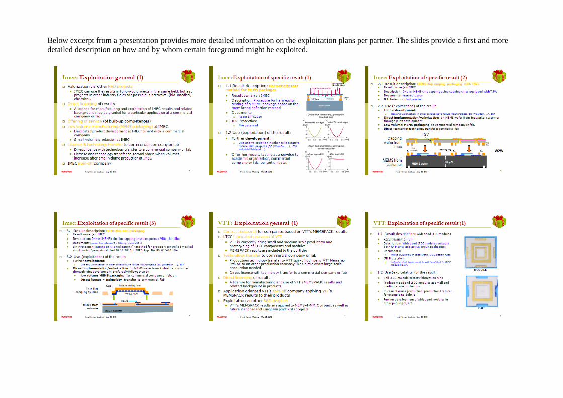
Below excerpt from a presentation provides more detailed information on the exploitation plans per partner. The slides provide a first and more
detailed description on how and by whom certain foreground might be exploited.
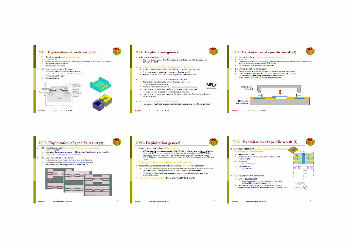

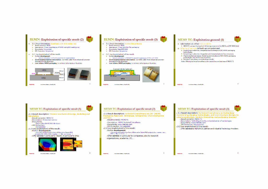
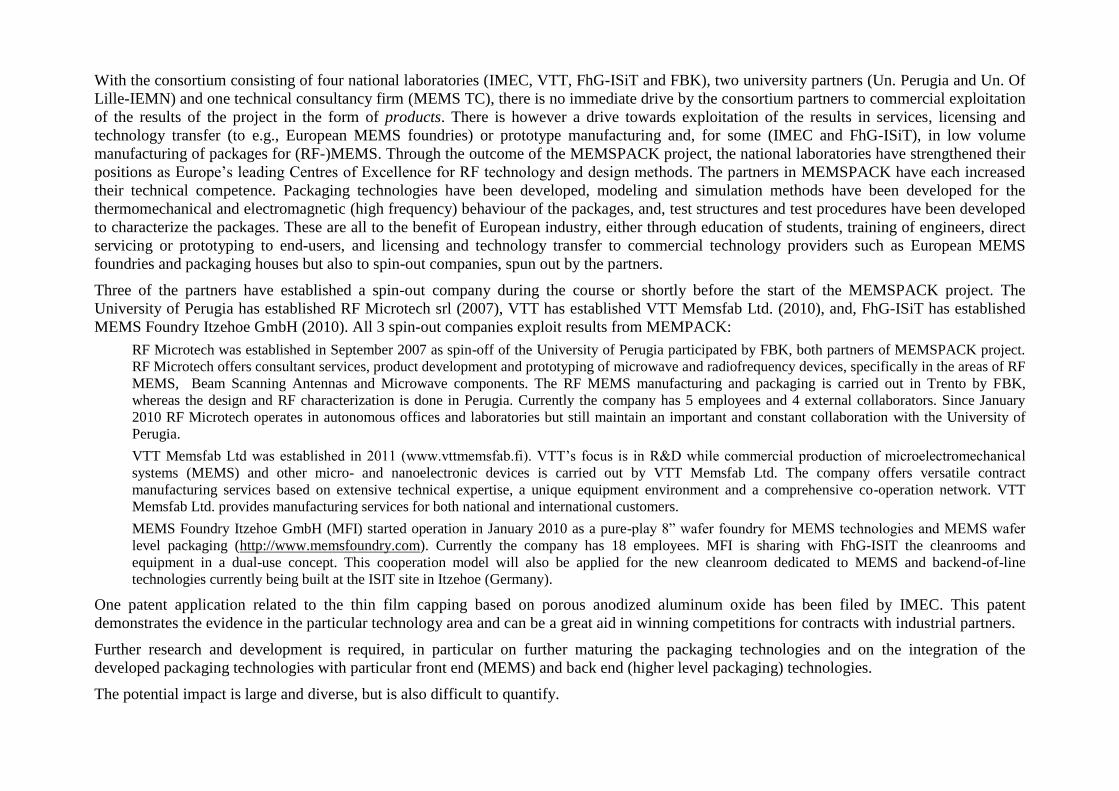
With the consortium consisting of four national laboratories (IMEC, VTT, FhG-ISiT and FBK), two university partners (Un. Perugia and Un. Of
Lille-IEMN) and one technical consultancy firm (MEMS TC), there is no immediate drive by the consortium partners to commercial exploitation
of the results of the project in the form of products. There is however a drive towards exploitation of the results in services, licensing and
technology transfer (to e.g., European MEMS foundries) or prototype manufacturing and, for some (IMEC and FhG-ISiT), in low volume
manufacturing of packages for (RF-)MEMS. Through the outcome of the MEMSPACK project, the national laboratories have strengthened their
positions as Europe’s leading Centres of Excellence for RF technology and design methods. The partners in MEMSPACK have each increased
their technical competence. Packaging technologies have been developed, modeling and simulation methods have been developed for the
thermomechanical and electromagnetic (high frequency) behaviour of the packages, and, test structures and test procedures have been developed
to characterize the packages. These are all to the benefit of European industry, either through education of students, training of engineers, direct
servicing or prototyping to end-users, and licensing and technology transfer to commercial technology providers such as European MEMS
foundries and packaging houses but also to spin-out companies, spun out by the partners.
Three of the partners have established a spin-out company during the course or shortly before the start of the MEMSPACK project. The
University of Perugia has established RF Microtech srl (2007), VTT has established VTT Memsfab Ltd. (2010), and, FhG-ISiT has established
MEMS Foundry Itzehoe GmbH (2010). All 3 spin-out companies exploit results from MEMPACK:
RF Microtech was established in September 2007 as spin-off of the University of Perugia participated by FBK, both partners of MEMSPACK project.
RF Microtech offers consultant services, product development and prototyping of microwave and radiofrequency devices, specifically in the areas of RF
MEMS, Beam Scanning Antennas and Microwave components. The RF MEMS manufacturing and packaging is carried out in Trento by FBK,
whereas the design and RF characterization is done in Perugia. Currently the company has 5 employees and 4 external collaborators. Since January
2010 RF Microtech operates in autonomous offices and laboratories but still maintain an important and constant collaboration with the University of
Perugia.
VTT Memsfab Ltd was established in 2011 (www.vttmemsfab.fi). VTT’s focus is in R&D while commercial production of microelectromechanical
systems (MEMS) and other micro- and nanoelectronic devices is carried out by VTT Memsfab Ltd. The company offers versatile contract
manufacturing services based on extensive technical expertise, a unique equipment environment and a comprehensive co-operation network. VTT
Memsfab Ltd. provides manufacturing services for both national and international customers.
MEMS Foundry Itzehoe GmbH (MFI) started operation in January 2010 as a pure-play 8” wafer foundry for MEMS technologies and MEMS wafer
level packaging (http://www.memsfoundry.com). Currently the company has 18 employees. MFI is sharing with FhG-ISIT the cleanrooms and
equipment in a dual-use concept. This cooperation model will also be applied for the new cleanroom dedicated to MEMS and backend-of-line
technologies currently being built at the ISIT site in Itzehoe (Germany).
One patent application related to the thin film capping based on porous anodized aluminum oxide has been filed by IMEC. This patent
demonstrates the evidence in the particular technology area and can be a great aid in winning competitions for contracts with industrial partners.
Further research and development is required, in particular on further maturing the packaging technologies and on the integration of the
developed packaging technologies with particular front end (MEMS) and back end (higher level packaging) technologies.
The potential impact is large and diverse, but is also difficult to quantify.

4.3 Report on societal implications
Replies to the following questions will assist the Commission to obtain statistics and
indicators on societal and socio-economic issues addressed by projects. The questions are
arranged in a number of key themes. As well as producing certain statistics, the replies will
also help identify those projects that have shown a real engagement with wider societal issues,
and thereby identify interesting approaches to these issues and best practices. The replies for
individual projects will not be made public.
A General Information (completed automatically when Grant Agreement number
is entered.
Grant Agreement Number: 223882
Title of Project: MEMSPACK
Name and Title of Coordinator: Dr. Harrie Tilmans (IMEC), Principal Scientist
B Ethics
1. Did your project undergo an Ethics Review (and/or Screening)?
If Yes: have you described the progress of compliance with the relevant Ethics
Review/Screening Requirements in the frame of the periodic/final project reports?
Special Reminder: the progress of compliance with the Ethics Review/Screening Requirements
should be described in the Period/Final Project Reports under the Section 3.2.2 'Work Progress
and Achievements'
0Yes 0 No
2. Please indicate whether your project involved any of the following
issues (tick box) : None of
the below
RESEARCH ON HUMANS
Did the project involve children?
Did the project involve patients?
Did the project involve persons not able to give consent?
Did the project involve adult healthy volunteers?
Did the project involve Human genetic material?
Did the project involve Human biological samples?
Did the project involve Human data collection?
RESEARCH ON HUMAN EMBRYO/FOETUS
Did the project involve Human Embryos?
Did the project involve Human Foetal Tissue / Cells?
Did the project involve Human Embryonic Stem Cells (hESCs)?
Did the project on human Embryonic Stem Cells involve cells in culture?
Did the project on human Embryonic Stem Cells involve the derivation of cells from
Embryos?
PRIVACY
Did the project involve processing of genetic information or personal data (eg. health,
sexual lifestyle, ethnicity, political opinion, religious or philosophical conviction)?
Did the project involve tracking the location or observation of people?
RESEARCH ON ANIMALS
Did the project involve research on animals?
Were those animals transgenic small laboratory animals?
X

Were those animals transgenic farm animals?
Were those animals cloned farm animals?
Were those animals non-human primates?
RESEARCH INVOLVING DEVELOPING COUNTRIES
Did the project involve the use of local resources (genetic, animal, plant etc)?
Was the project of benefit to local community (capacity building, access to healthcare,
education etc)?
DUAL USE
Research having direct military use 0 Yes 0 No
Research having the potential for terrorist abuse
C Workforce Statistics
3. Workforce statistics for the project: Please indicate in the table below the number
of people who worked on the project (on a headcount basis). Note: people have not been
counted twice, e.g., if WP leader is experienced researcher then this is not added to the experienced researchers.
Type of Position Number of Women Number of
Men
Scientific Coordinator 0 1
Work package leaders 2 6
Experienced researchers (i.e. PhD holders) 3 25
PhD Students 0 4
Other 9 15
4. How many additional researchers (in companies and universities)
were recruited specifically for this project? 1
Of which, indicate the number of men: 1
X

D Gender Aspects
5. Did you carry out specific Gender Equality Actions under the
project?
Yes
No
6. Which of the following actions did you carry out and how effective were they?
Not at all
effective
Very
effective
Design and implement an equal opportunity policy Set targets to achieve a gender balance in the workforce Organise conferences and workshops on gender Actions to improve work-life balance Other:
7. Was there a gender dimension associated with the research content – i.e. wherever
people were the focus of the research as, for example, consumers, users, patients or in trials, was
the issue of gender considered and addressed?
Yes- please specify
No
E Synergies with Science Education
8. Did your project involve working with students and/or school pupils (e.g. open
days, participation in science festivals and events, prizes/competitions or joint
projects)?
Yes- please specify
No
9. Did the project generate any science education material (e.g. kits, websites,
explanatory booklets, DVDs)?
Yes- please specify
No
F Interdisciplinarity
10. Which disciplines (see list below) are involved in your project?
Main discipline5: 2 (2.2&2.3)
Associated discipline5: Associated discipline
5:
G Engaging with Civil society and policy makers
11a Did your project engage with societal actors beyond the
research community? (if 'No', go to Question 14)
Yes
No
11b If yes, did you engage with citizens (citizens' panels / juries) or organised civil
society (NGOs, patients' groups etc.)?
No
Yes- in determining what research should be performed
Yes - in implementing the research
Yes, in communicating /disseminating / using the results of the project
5 Insert number from list below (Frascati Manual).
X
X X
X
X
X
X Lectures in university curriculums,
and in summer schools
Presentation slides summer schools
X
X
X

11c In doing so, did your project involve actors whose role is mainly to
organise the dialogue with citizens and organised civil society (e.g.
professional mediator; communication company, science museums)?
Yes
No
12. Did you engage with government / public bodies or policy makers (including
international organisations)
No
Yes- in framing the research agenda
Yes - in implementing the research agenda
Yes, in communicating /disseminating / using the results of the project
13a Will the project generate outputs (expertise or scientific advice) which could be
used by policy makers?
Yes – as a primary objective (please indicate areas below- multiple answers possible)
Yes – as a secondary objective (please indicate areas below - multiple answer possible)
No
13b If Yes, in which fields?
Agriculture Audiovisual and Media
Budget
Competition Consumers
Culture
Customs Development Economic and
Monetary Affairs
Education, Training, Youth
Employment and Social Affairs
Energy Enlargement
Enterprise
Environment External Relations
External Trade
Fisheries and Maritime Affairs Food Safety
Foreign and Security Policy
Fraud
Humanitarian aid
Human rights Information Society
Institutional affairs
Internal Market Justice, freedom and security
Public Health
Regional Policy Research and Innovation
Space
Taxation
Transport
13c If Yes, at which level?
Local / regional levels
National level
European level
International level
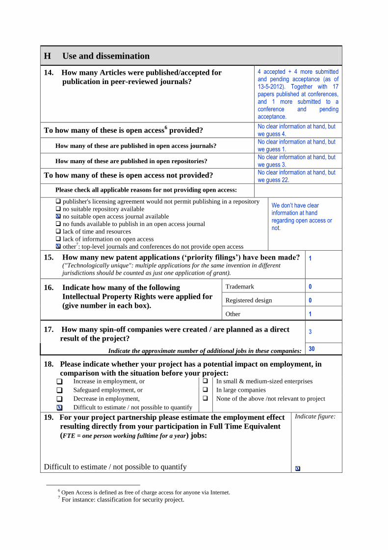
H Use and dissemination
14. How many Articles were published/accepted for
publication in peer-reviewed journals?
4 accepted + 4 more submitted and pending acceptance (as of 13-5-2012). Together with 17 papers published at conferences, and 1 more submitted to a conference and pending acceptance.
To how many of these is open access6 provided?
No clear information at hand, but we guess 4.
How many of these are published in open access journals? No clear information at hand, but we guess 1.
How many of these are published in open repositories? No clear information at hand, but we guess 3.
To how many of these is open access not provided? No clear information at hand, but we guess 22.
Please check all applicable reasons for not providing open access:
publisher's licensing agreement would not permit publishing in a repository
no suitable repository available
no suitable open access journal available
no funds available to publish in an open access journal
lack of time and resources
lack of information on open access
other7: top-level journals and conferences do not provide open access
We don’t have clear information at hand regarding open access or not.
15. How many new patent applications (‘priority filings’) have been made? ("Technologically unique": multiple applications for the same invention in different
jurisdictions should be counted as just one application of grant).
1
16. Indicate how many of the following
Intellectual Property Rights were applied for
(give number in each box).
Trademark 0
Registered design 0
Other 1
17. How many spin-off companies were created / are planned as a direct
result of the project? 3
Indicate the approximate number of additional jobs in these companies: 30
18. Please indicate whether your project has a potential impact on employment, in
comparison with the situation before your project: Increase in employment, or In small & medium-sized enterprises
Safeguard employment, or In large companies
Decrease in employment, None of the above /not relevant to project
Difficult to estimate / not possible to quantify
19. For your project partnership please estimate the employment effect
resulting directly from your participation in Full Time Equivalent
(FTE = one person working fulltime for a year) jobs:
Difficult to estimate / not possible to quantify
Indicate figure:
6 Open Access is defined as free of charge access for anyone via Internet. 7 For instance: classification for security project.
X
X
X
X

I Media and Communication to the general public
20. As part of the project, were any of the beneficiaries professionals in
communication or media relations?
Yes No
21. As part of the project, have any beneficiaries received professional media /
communication training / advice to improve communication with the general
public?
Yes No
22 Which of the following have been used to communicate information about your
project to the general public, or have resulted from your project?
Press Release Coverage in specialist press
Media briefing Coverage in general (non-specialist) press
TV coverage / report Coverage in national press
Radio coverage / report Coverage in international press
Brochures /posters / flyers Website for the general public / internet
DVD /Film /Multimedia Event targeting general public (festival,
conference, exhibition, science café)
23 In which languages are the information products for the general public produced?
Language of the coordinator English
Other language(s)
Question F-10: Classification of Scientific Disciplines according to the Frascati Manual 2002 (Proposed
Standard Practice for Surveys on Research and Experimental Development, OECD 2002):
FIELDS OF SCIENCE AND TECHNOLOGY
1. NATURAL SCIENCES
1.1 Mathematics and computer sciences [mathematics and other allied fields: computer sciences and other
allied subjects (software development only; hardware development should be classified in the
engineering fields)]
1.2 Physical sciences (astronomy and space sciences, physics and other allied subjects)
1.3 Chemical sciences (chemistry, other allied subjects)
1.4 Earth and related environmental sciences (geology, geophysics, mineralogy, physical geography and
other geosciences, meteorology and other atmospheric sciences including climatic research,
oceanography, vulcanology, palaeoecology, other allied sciences)
1.5 Biological sciences (biology, botany, bacteriology, microbiology, zoology, entomology, genetics,
biochemistry, biophysics, other allied sciences, excluding clinical and veterinary sciences)
2 ENGINEERING AND TECHNOLOGY
2.1 Civil engineering (architecture engineering, building science and engineering, construction engineering,
municipal and structural engineering and other allied subjects)
2.2 Electrical engineering, electronics [electrical engineering, electronics, communication engineering and
systems, computer engineering (hardware only) and other allied subjects]
2.3. Other engineering sciences (such as chemical, aeronautical and space, mechanical, metallurgical and
materials engineering, and their specialised subdivisions; forest products; applied sciences such as
geodesy, industrial chemistry, etc.; the science and technology of food production; specialised
technologies of interdisciplinary fields, e.g. systems analysis, metallurgy, mining, textile technology
and other applied subjects)
X
X
X
X X
X

3. MEDICAL SCIENCES
3.1 Basic medicine (anatomy, cytology, physiology, genetics, pharmacy, pharmacology, toxicology,
immunology and immunohaematology, clinical chemistry, clinical microbiology, pathology)
3.2 Clinical medicine (anaesthesiology, paediatrics, obstetrics and gynaecology, internal medicine, surgery,
dentistry, neurology, psychiatry, radiology, therapeutics, otorhinolaryngology, ophthalmology)
3.3 Health sciences (public health services, social medicine, hygiene, nursing, epidemiology)
4. AGRICULTURAL SCIENCES
4.1 Agriculture, forestry, fisheries and allied sciences (agronomy, animal husbandry, fisheries, forestry,
horticulture, other allied subjects)
4.2 Veterinary medicine
5. SOCIAL SCIENCES
5.1 Psychology
5.2 Economics
5.3 Educational sciences (education and training and other allied subjects)
5.4 Other social sciences [anthropology (social and cultural) and ethnology, demography, geography
(human, economic and social), town and country planning, management, law, linguistics, political
sciences, sociology, organisation and methods, miscellaneous social sciences and interdisciplinary ,
methodological and historical S1T activities relating to subjects in this group. Physical anthropology,
physical geography and psychophysiology should normally be classified with the natural sciences].
6. HUMANITIES
6.1 History (history, prehistory and history, together with auxiliary historical disciplines such as
archaeology, numismatics, palaeography, genealogy, etc.)
6.2 Languages and literature (ancient and modern)
6.3 Other humanities [philosophy (including the history of science and technology) arts, history of art, art
criticism, painting, sculpture, musicology, dramatic art excluding artistic "research" of any kind,
religion, theology, other fields and subjects pertaining to the humanities, methodological, historical and
other S1T activities relating to the subjects in this group]